

Page 1

Samsung Electronics 1-1
1. Be sure that all of the built-in protective devices
are replaced. Restore any missing protective
shields.
2. When reinstalling the chassis and its assemblies, be sure to restore all protective devices,
including :
control knobs and compartment covers.
3. Make sure that there are no cabinet openings
through which people--particularly children
--might insert fingers and contact dangerous
voltages. Such openings include the spacing
between the picture tube and the cabinet mask,
excessively wide cabinet ventilation slots, and
improperly fitted back covers.
If the measured resistance is less than 1.0
megohm or greater than 5.2 megohms, an
abnormality exists that must be corrected
before the unit is returned to the customer.
4. Leakage Current Hot Check (See Fig. 1) :
Warning : Do not use an isolation transformer
during this test. Use a leakage current tester or
a metering system that complies with American
National Standards Institute (ANSI C101.1,
Leakage Current for Appliances), and
Underwriters Laboratories (UL Publication
UL1410, 59.7).
5. With the unit completely reassembled, plug the
AC line cord directly the power outlet. With the
unit’s AC switch first in the ON position and
then OFF, measure the current between a
known earth ground (metal water pipe, conduit, etc.) and all exposed metal parts, including : antennas, handle, brackets, metal cabinets,
screwheads and control shafts. The current
measured should not exceed 0.5 milliamp.
Reverse the power-plug prongs in the AC outlet and repeat the test.
6. X-ray Limits :
The picture tube is designed to prohibit X-ray
emissions. To ensure continued X-ray protection, replace the picture tube only with one that
is the same type as the original.
Fig. 1 AC Leakage Test
7. Antenna Cold Check :
With the unit’s AC plug disconnected from the
AC source, connect an electrical jumper across
the two AC prongs. Connect one lead of the
ohmmeter to an AC prong.
Connect the other lead to the coaxial connector.
8. High Voltage Limit :
High voltage must be measured each time
servicing is done on the B+, horizontal deflection or high voltage circuits.
Heed the high voltage limits. These include the
X-ray protection Specifications Label, and the
Product Safety and X-ray Warning Note on the
service data schematic.
9. Some semiconductor (“solid state”) devices are
easily damaged by static electricity.
Such components are called Electrostatically
Sensitive Devices (ESDs); examples include
integrated circuits and some field-effect transistors.
The following techniques will reduce the
occurrence of component damage caused by
static electricity.
10. Immediately before handling any semiconduc-
tor components or assemblies, drain the electrostatic charge from your body by touching a
known earth ground. Alternatively, wear a discharging Wrist-strap device. (Be sure to
remove it prior to applying power--this is an
electric shock precaution.)
1. Precautions
Device
Under
Test
(Reading should
not be above
0.5mA)
Leakage
Currant
Tester
Earth
Ground
Test all
exposed metal
surfaces
Also test with
plug reversed
(using AC adapter
plug as required)
2-Wire Cord
Page 2

11. High voltage is maintained within specified
limits by close-tolerance, safety-related components and adjustments. If the high voltage
exceeds the specified limits, check each of the
special components.
12. Design Alteration Warning :
Never alter or add to the mechanical or electrical design of this unit. Example : Do not
add auxiliary audio or video connectors. Such
alterations might create a safety hazard. Also,
any design changes or additions will void the
manufacturer’s warranty.
13. Hot Chassis Warning :
Some TV receiver chassis are electrically
connected directly to one conductor of the AC
power cord. If an isolation transformer is not
used, these units may be safely serviced only
if the AC power plug is inserted so that the
chassis is connected to the ground side of the
AC source.
To confirm that the AC power plug is inserted
correctly, do the following : Using an AC
voltmeter, measure the voltage between the
chassis and a known earth ground. If the reading is greater than 1.0V, remove the AC power
plug, reverse its polarity and reinsert. Re-measure the voltage between the chassis and
ground.
14. Some TV chassis are designed to operate with
85 volts AC between chassis and ground,
regardless of the AC plug polarity. These units
can be safely serviced only if an isolation transformer inserted between the receiver and the
power source.
15. Never defeat any of the B+ voltage interlocks.
Do not apply AC power to the unit (or any of
its assemblies) unless all solid-state heat sinks
are correctly installed.
16. Always connect a test instrument’s ground
lead to the instrument chassis ground before
connecting the positive lead; always remove
the instrument’s ground lead last.
17. Observe the original lead dress, especially near
the following areas : Antenna wiring, sharp
edges, and especially the AC and high voltage
power supplies. Always inspect for pinched,
out-of-place, or frayed wiring. Do not change
the spacing between components and the
printed circuit board. Check the AC power
cord for damage. Make sure that leads and
components do not touch thermally hot parts.
18. Picture Tube Implosion Warning :
The picture tube in this receiver employs
“integral implosion” protection. To ensure
continued implosion protection, make sure
that the replacement picture tube is the same
as the original.
19. Do not remove, install or handle the picture
tube without first putting on shatterproof goggles equipped with side shields. Never handle
the picture tube by its neck. Some “in-line”
picture tubes are equipped with a permanently
attached deflection yoke; do not try to remove
such “permanently attached” yokes from the
picture tube.
20. Product Safety Notice :
Some electrical and mechanical parts have
special safety-related characteristics which
might not be obvious from visual inspection.
These safety features and the protection they
give might be lost if the replacement component differs from the original--even if the
replacement is rated for higher voltage,
wattage, etc.
Components that are critical for safety are
indicated in the circuit diagram by shading,
( or ).
Use replacement components that have the
same ratings, especially for flame resistance
and dielectric strength specifications.
A replacement part that does not have the
same safety characteristics as the original
might create shock, fire or other hazards.
Samsung Electronics1-2
Precautions
Page 3

Samsung Electronics 2-1
2. Product Specifications and Comparison Chart
2-1 NTSC Model (SCL500/L520/L530/L550)
Recording system
Video signal
Usable cassette
Tape speed
Speed mode
Recording time
FF or REW time
Image device
Optical zoom ratio
Focal lengh: f
F
Filter diameter
Focus system
Macro
Min. Illumination
Connectors
Video out
Audio out
External mic
General
Power requirement
Power consumption
Built-in mic
Operating temperature
Dimension (W x H x D)
Weight
System
SCL500/L520/L530/L550
Video: 2 rotary heads Helical scanning FM
Audio: FM monaural system
NTSC color, EIAstandard
SCL500/L520/L530 : 8mm SCL550 : Hi8 or 8mm
SP:14.345 mm/sec
Record: SP only, Playback: SP and LP
P6-120: 120 min.
P6-120: approx. 6.5 min.
CCD(Charge Coupled Device)
22X
3.6 ~ 79.2 mm
1.6
46 mm
Inner
Auto wide macro
0.3 lux (visible)
Mini jack, 1 Vp-p, 75 ohms, Unbalanced
Mini jack 7.7 dBs, imp.: less than 1.8 K ohms
Monaural,
Ø3.5
7.4 ~ 8.4 V DC
SCL500/L520: 4.3W, SCL530: 4.7W, SCL550: 5.3W
Condenser mic, omni-directional
0°C to 40°C (32°F to 104°F)
101 x 104 x 176 (mm) ; 3.98 x 4.09 x 6.93 (inch)
760g (1.675 lbs)
Page 4
Samsung Electronics2-2
Products Specifications and Comparison Chart
2-2 PAL Model (VP-L500/L520/L530/L530B/L550)
✤ The technical specifications and design may be changed without notice.
Recording system
Video signal
Usable cassette
Tape speed
Speed mode
Recording time
FF or REW time
Image device
Optical zoom ratio
Focal lengh: f
F
Filter diameter
Focus system
Macro
Min. Illumination
Connectors
Video out
Audio out
External mic
General
Power requirement
Power consumption
Built-in mic
Operating temperature
Dimension (W x H x D)
Weight
System
VP-L500/L520/L530/L530B/L550
Video: 2 rotary heads Helical scanning FM
Audio: FM monaural system
PAL color, CCIR standard
VP-L500/L520/L530/L530B: 8mm
VP-L550: Hi8 or 8mm
SP: 20.051 mm/sec
Record: SP only, Playback: SP and LP
P5-120: 120 min.
P5-120: approx. 8 min.
CCD(Charge Coupled Device)
22X
3.6 ~ 79.2 mm
1.6
46 mm
Inner
Auto wide macro
0.3 lux (visible)
Mini jack, 1 Vp-p, 75 ohms, Unbalanced
Mini jack 7.7 dBs, imp.: less than 1.8 K ohms
Monaural,
Ø3.5
7.4 ~ 8.4 V DC
VP-L500/L520: 4.3W, VP-L530/L530B: 4.7W, VP-L550: 5.3W
Condenser mic, omni-directional
0°C to 40°C
101 x 104 x 176 (mm)
760g
Page 5
Samsung Electronics 2-3
Products Specifications and Comparison Chart
2-3 Comparison Chart
Features
Model
Format
SCL520
8mm
SCL530
8mm
SCL550
X
Li-ion
O
X
X
EVF
X
Video Light
Battery
BLC
Remote Control
XDR
Viewfinder
DIS
X
X
SNAP/SHOT
PIP
NTSC
X
Li-ion
O
O
X
EVF
O
O
O
Hi8
X
Li-ion
O
O
X
EVF
O
O
O
270K
CCD
270K
410K
SCL500
8mm
X
Li-ion
O
X
X
EVF
X
X
X
270K
220X 440X 440X 440XDigital Zoom Ratio
Features
Model
Format
VP-L500 VP-L520 VP-L530 VP-L530B
Video Light
Battery
BLC
Remote Control
XDR
Viewfinder
DIS
SNAP/SHOT
PIP
PAL
CCD
8mm
X
Li-ion
O
X
X
EVF
X
X
X
320K
440X
8mm
X
Li-ion
O
O
X
EVF
X
X
X
320K
440X
8mm
X
Li-ion
O
O
X
EVF
X
X
X
320K
440X
8mm
X
Li-ion
O
O
X
EVF
O
O
O
320K
440X
Hi8
X
Li-ion
O
O
O
EVF
O
O
O
470K
440X
Digital Zoom Ratio
VP-L550
Page 6

MEMO
MEMO
Products Specifications and Comparison Chart
Samsung Electronics2-4
Page 7

Samsung Electronics 3-1
3. Disassembly and Reassembly
3-1. Cabinet and PCB
3-1-1 Ass’y Cover Housing Removal
2
Remove the ass’y cover
housing in the direction
of arrow .
"A"
A
1
REMOVE 2 SCREWS.
Fig. 3-1 Ass’y Cover Housing Removal
Page 8

3-1-2 Ass’y Case Top Removal
Samsung Electronics3-2
Disassembly and Reassembly
1
REMOVE CASE TOP BY GENTLELY RELEASING
1 LOCKING TABS WITH A SMALL SCREW DRIVER.
(SEE DETAIL "A")
REASSEMBLY : PUT THE 4 TABS INTO THE SLOT,
WHILE SLIDING IT AS SHOWN IN DETAIL "B".
1 LOCKING TAB
PRECISION
SCREW DRIVER
< DETAIL "A" >
"B"
< DETAIL "B" >
Fig. 3-2 Ass’y Case Top Removal
Page 9

Samsung Electronics 3-3
Disassembly and Reassembly
3-1-3 Ass’y Front Removal
1
REMOVE 2 SCREWS.
1
2
REMOVE THE ASS’Y FRONT IN
THE DIRECTION OF ARROW "A".
3
PISCOANECT THE CONNECTOR
FROM THE MAIN PCB.
"A"
Fig.3-3 Ass’y Front Removal
Page 10
3-1-4 Ass’y Case Left Removal
Samsung Electronics3-4
Disassembly and Reassembly
2
REMOVE THE ASS’Y CASE Right
IN THE DIRECTION OF ARROW "A".
5
3
4
REMOVE 2 SCREWS.
DISASSEMBLE AFTER TURNING
KNOB to be "LOCK".
REMOVE 3 SCREWS.
1
REMOVE 1 SCREWS.
"A"
Fig. 3-4 Ass’y Case Left Removal
Page 11

Samsung Electronics 3-5
Disassembly and Reassembly
3-1-5 Ass’y Case Right Removal
2
PULL OUT THE CASE LEFT
ASSEMBLY IN THE DIRECTION
OF ARROW "A" .
DISCONNECT FPC FROM THE
CONNECTOR OF THE MAIN PCB.
REMOVE 1 SCREWS.
1
REMOVE 4 SCREWS.
1
"A"
1
1
1
Fig. 3-5 Ass’y Case Right Removal
Page 12

Samsung Electronics3-6
Disassembly and Reassembly
3-1-6 Ass’y LCD Removal
REMOVE THE LCD ASS’Y
IN THE DIRECTION OF ARROW.
REMOVE 3 SCREWS.
REMOVE THE COVER BOTTOM ASS’Y
IN THE DIRECTION OF ARROW "A".
REMOVE 3 SCREWS.
1
2
3
4
"A"
Fig. 3-6 Ass’y LCD Removal
Page 13
Samsung Electronics 3-7
Disassembly and Reassembly
3-1-7 Ass’y EVF Removal
4
REMOVE THE EVF ASS’Y
IN THE DIRECTION OF ARROW.
1
REMOVE 3 SCREW.
2
REMOVE THE COVER LEFT TOP ASS’Y
IN THE DIRECTION OF ARROW.
3
REMOVE 6 SCREWS.
Fig. 3-7 Ass’y EVF Removal
Page 14
Samsung Electronics3-8
Disassembly and Reassembly
3-1-8 Ass’y Rear Board Removal
2
REMOVE THE ASS’Y FUNCTION
BOARD IN THE DIRECTION OF
ARROW "A".
1
REMOVE 2 SCREWS.
"A"
Fig. 3-8 Ass’y Rear Board Removal
Page 15

Samsung Electronics 3-9
Disassembly and Reassembly
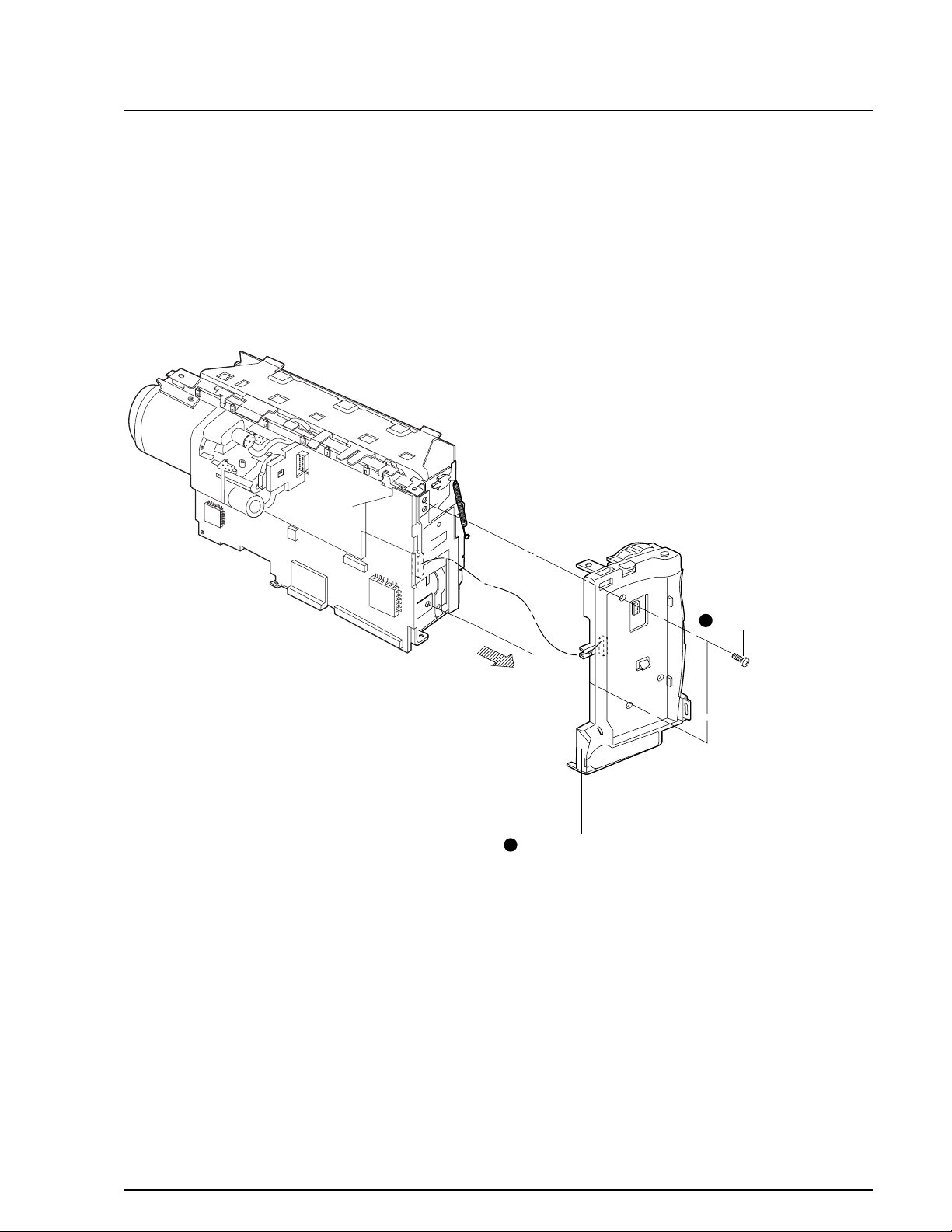
3-1-9 Ass’y Deck and Main PCB Removal
DISCONNECTOR THE FPC
FROM THE MAIN PCB.
REMOVE THE 2 SCREWS.
DISCONNECT CONNECTOR
FROM THE HEAD-DRUM.
1
PULL OUT THE MAIN POB FROM THE
ASS’Y DECK IN THE DIRATION OF
ARROW "A".
2
"A"
Fig. 3-9 Ass’y Deck and Main PCB Removal
Page 16

Samsung Electronics3-10
Disassembly and Reassembly
3-1-10 Ass’y Camera Removal
1
REMOVE 2 SCREWS.
3
DISCONNECT FPC FROM THE
CONNECTOR OF THE MAIN PCB.
2
REMOVESDLDER WITH
AN IRON TO ISOPATE
SHIELD-CASE AND LENS.
DISCONNECTOR CONNECTOR AND PULL OUT THE
ASS’Y LENS IN THE DIRECTION OF ARROW "A".
"A"
Fig. 3-10 Ass’y Camera Removal
Page 17

Samsung Electronics 3-11
Disassembly and Reassembly
3-2. Circuit Boards Location
Fig. 3-11 Circuit Boards Location
ASS’Y MAIN BOARD
ASS’Y FRONT BOARD
ASS’Y FUNCTION BOARD
ASS’Y REAR BOARD
Page 18

Samsung Electronics3-12
Disassembly and Reassembly
3-3. Connector Diagram
Fig. 3-12 Connector Diagrams
NO. NO.CONNECTOR
CONNECTOR
DIRECTION
DECK FPC CN501
DECK MAIN PCB
DRUM HEAD FPC CN52
CN601 CN451
CNP02
CNP01 CNC01
CN701 CN801
CN602
CN802 MIC CONNECTOR
CN473
EVF FPC
CN471
DECK MAIN PCB
MAIN PCB REAR PCB
MAIN PCB ASS’Y LENS PCB
MAIN PCB CCD PCB
MAIN PCB FRONT PCB
MAIN PCB FUNCTION PCB
FRONT PCB ASS’Y MIC
FUNCTION PCB ASS’Y EVF
LENS FPC
SPEAKER CONNECTOR
CN475
LCD CONNECTOR
CN474
SPEAKER ASS’Y FUNCTION PCB
LCD ASS’Y FUNCTION PCB
Page 19

• Refer to mechanical manual “DE-6 (AD68-30200A)”for the adjustment and checks of mechanism section.
• The location of test point (See Fig.1)
Samsung Electronics 4-1
Alignment and Adjustment
4. Alignment and Adjustment
4-1. Mechanism Alignment
Test Point:
PB RF - Pin 11 of CN452
Head Switching Trigger - Pin 9 of CN452
Fig. 2 Test location of test point (Rear Board)
CN452
PB RF
Head Switching - Trigger
CN452
Fig. 1 Test point
SW471
J451
DC-JACK
BAT-TERMINAL
(+)
BAT-TERMINAL
(-)
14 13
12 11
10 9
87
65
43
21
Page 20

Samsung Electronics4-2
Alignment and Adjustment
POSITION
IC601 IC601 IC601
ACTION MODE
28PIN 27PIN 26PIN
L H H EJECT
L L H UNLOADING STOP
H L L LOADING STOP
H H L PLAY, FF, REW, STILL....
EJECT
UNLOADING STOP
LOADING STOP
PB
IC601
27PIN
GROUND
IC601
26PIN
COMMON
IC601
28PIN
OPEN
EJECT
PLAY
LOADING
STOP
UNLOADING
STOP
LOADING
UNLOADING
Page 21

Samsung Electronics 4-3
Alignment and Adjustment
Note :
1. This system has :
1) EEPROM to store the confirmed adjustment data.
2) DSP (Digital Signal Process ; ICP01 - Main board) chip to process the signal of camera parts.
3) One test point for the frequency adjustment of DSP main clock (P. CLK).
4) The special mode for camera adjustment using the function keys on the left case.
2. Keep in mind :
1) All adjustment steps should performed using the function keys on the left case.
4-2-1 Preparations
4. The Function keys on the left case :
The following is a chart explaining the use of each button :
4-2. Camera Section Adjustment
1. Equipment to be used :
1) DC Power supply
2) Oscilloscope
3) Frequency counter
4) Vectorscope
5) Waveform monitor
6) Color monitor or TV
7) Various charts
- Color bar chart
- Gray-scale chart, etc...
2. Composition of camera P.C.Boards :
1) Main PCB 2) CCD PCB
3) CVF PCB 4) EVF PCB 5) LCD PCB
3. Adjustment preparations :
1) The function keys on the left case is used as a
camera adjust tool.
2) Press the confirm button when each manual
adjustment step is completed to write the
adjustment data to the EEPROM.
3) After each adjustment step is completed, OSD
shows “OK!”.
4) To cancel the adjustment mode, remove the
power source.
Using Button
PROGRAM AE (CONFIRM)
TITLE (DATA DOWN)
DSE (DATA UP)
FADE (MODE UP)
BLC (MODE DOWN)
MANUAL FOCUS RING (NEAR/FAR)
ZOOM TELE
ZOOM WIDE
Adjustment
Data store after finishing adjustment by DATA UP/DOWN button.
When change data value of adjust state.
Mode change.
Manual focus adjustment.
1) Move the zoom position of lens.
2) Semi-Auto lens adjustment.
Page 22

Samsung Electronics4-4
Alignment and Adjustment
The function keys left case is required to adjust the camera section.
Note : In service adjustment mode, button names are different from those in customer camera function
control mode. EX) PROGRAM AE button is the same as confirm.
5. How to get into service “ADJUST” mode
1. Remove the lithium battery from the
camcorder.
2. Connect the power source (battery/
DC cable).
3. Eject the tape if it is in the unit.
4. Set the power switch of the
camcorder to “CAMERA” position.
5. Set OSD on state.
STEP 1
1. Press and hold the “EJECT” button and
“DATE/TIME” button on the camcorder at the
same time for more than 5 seconds.
Then unit goes into service mode.
STEP 2
On screen display show “0DF. T.INI XX XX”
CAMERAADJUSTMENT mode has successfully been activated.
STEP 3
Note : When “XX XX” is shown in service adjustment procedures, this indicates variable values.
EJECT
MODE DOWN
MODE UP
Confirm
DATA UP
DATA DOWN
FAR
NEAR
MANUAL
FOCUS
DATE/TIME
Page 23

Samsung Electronics 4-5
Alignment and Adjustment
001 40 50 40 50 CDS-K=1 AGC TARGET photo/E,ODD WDR/NO WDR_AE_O KEY/RING CAN/SECREM ZOOM_STOP
002 00 00 00 00 @IRIS CONTROL-LOW
003 06 06 06 06 @IRIS CONTROL-HIGH
004 60 60 60 60 @P.CLK PWM-HIGH
005 08 08 08 08 @UPD16835 INIT 4th
006 55 55 55 55 @UPD16835 INIT 6th
007 33 33 33 33 @UPD16835 INIT 7th
008 03 03 03 03 @CDS F-REG(f1,f0) CAM : BIT0:f0,BIT1:f1
009 A0 A0 A0 A0 @CDS F-REG(f9,f2) CAM ;PGA GAIN -HIGH(0.00dB~ 30.0dB)
00A 60 60 60 60 changeb by AUTO HALL ADJ (0CD) ;HALL REFERENCE
00B 3A 3A 3A 3A changeb by AUTO HALL ADJ (0CD) ;HALL GAIN
00C 87 87 87 87 @CDS E-R(e1,e0),J-R(j0),M-R;D0:e0,D1:e1,D2:j0(CAM),D4:e0,D5:e1,D6:j0(VCR),D7:cds-rev='1'
00D 80 7B 77 77 @CDS F-REG(f9,f2) VCR ;PGA GAIN -HIGH(0.00dB~ 10.0dB)
00E 00 00 00 00 @WDR REGISTER[7,0] *AEINSEL=D7,AELPFSEL=D6,X[5:0]
00F 80 80 80 80 @WDR REGISTER[15,8] *AECLIP_TH[7:0]
010 00 00 00 00 @WDR REGISTER[23,16] *AEL_TH[7:0]
011 FF FF FF FF @WDR REGISTER[31,24] *AEH_TH[7:0]
012 76 76 8B 8B @WDR REGISTER[39,32] *AEW2VE[7:0]
013 24 24 24 24 @WDR REGISTER[47,40] *AEW2VS[7:0]
014 F1 F1 ED ED @WDR REGISTER[55,48] *AEW2HE[7:0]
015 13 13 07 07 @WDR REGISTER[63,56] *AEW2HS[7:0]
016 6E 6E 81 81 @WDR REGISTER[71,64] *AEW1VE[7:0]
017 20 20 26 26 @WDR REGISTER[79,72] *AEW1VS[7:0]
018 C1 C1 B4 B4 @WDR REGISTER[87,80] *AEW1HE[7:0]
019 43 43 32 32 @WDR REGISTER[95,88] *AEW1HS[7:0]
01A 30 30 30 30 @WDR REGISTER[103,96] *ALPF_THP[7:0]
01B 7F 7F 7F 7F @WDR REGISTER[111,104] *HLOG_ON[7],SAT_ON[6],ALPF_WTSTF[5:3],SHPF_SFT[2:0]
01C 80 80 80 80 @WDR REGISTER[119,112] *BOUND256[7:0]
01D 80 80 80 80 @WDR REGISTER[127,120] *BOUND128[7:0]
01E 80 80 80 80 @WDR REGISTER[135,128] *BOUND64[7:0]
01F 80 80 80 80 @WDR REGISTER[143,136] *BOUND32[7:0]
ADDR OSD-DISPLAY CONTENT
0DF T.INI TABLE INITIAL
0CD HALL HALL AUTO ADJUST
0CE IRIS IRIS AUTO ADJUST
0CF AWB AWB AUTO ADJUST
0D0 LENS LENS AUTO ADJUST( WARNING! DON’T USE WITHOUT AN INFINITE COLLIMATOR)
0D6 ZVR.C ZOOM LEVER CENTER DATA CHECKING
0DB AGCM AGC AUTO ADJUST (NORMALLY NO USED)
0DE 3MLENS 3M LENS AUTO ADJUST AT SERVICE FIELD (DISTANCE: 3M +/- 1Cm)
NO-OSD-DISPLAY DISTANCE
ADDR MODEL/DATA CONTENT
NTSC PAL
NOR HI8 NOR HI8 OPTION D6 D5 D4 D3 D2 D1 D0
“CAMERA ADJUST MODE, EEPROM ADDRESS SEQUENCE & DATA OF PAGE 0”
Page 24

NO-OSD-DISPLAY DISTANCE
ADDR MODEL/DATA CONTENT
NTSC PAL
NOR HI8 NOR HI8 OPTION D6 D5 D4 D3 D2 D1 D0
Samsung Electronics4-6
Alignment and Adjustment
020 60 60 60 60 @WDR REGISTER[151,144] *BOUND0[7:0]
021 3F 3F 3F 3F @WDR REGISTER[159,152] *LTIC[3:0],CH_SEL[3:0]
022 C7 C7 C7 C7 @WDR REGISTER[167,160] *LTI_ON[7],LSI_ON[6],LUT_TAB[5:3],LUT_HPF_SFT[2:0]
023 1E 1A 1E 1A @WDR REGISTER[175,168] *LUT_GAIN[7:0]
024 04 04 04 04 @WDR REGISTER[183,176] *BACK_WT[7:4],HIST_WT[3:0]
025 30 30 30 30 @WDR REGISTER[191,184] *EDGE_AMP[7:4],BACK_SP[3:0]
026 D0 D0 D0 D0 @WDR REGISTER[199,192] *LP_V[7:0] ACTIVE AREAVERTICAL LENGTH
027 24 24 24 24 @WDR REGISTER[207,200] *SP_V[7:0] ACTIVE AREA VERTICAL START
028 B0 B0 B0 B0 @WDR REGISTER[215,208] *LP_H[7:0] ACTIVE AREAHORIZENTAL LENGTH
029 30 30 30 30 @WDR REGISTER[223,216] *SP_H[7:0] ACTIVE AREAHORIZENTAL START
02A 00 00 00 00 @WDR REGISTER[231,224] *POFFSET[7:0]
02B 00 00 00 00 @WDR REGISTER[239,232] *CMP_ADJ[7:4],SP_ADJ[3:0]
02C 57 57 57 57 @WDR REGISTER[247,240] *CLPEN[7],SORSL[6],V1_EXIST[5],GR_MODE[4:3],GRB_MODE[2:0]
02D 01 01 01 01 @WDR REGISTER[255,248] *OUT_MODE[7:5],DLY_MODE[4:0]
02E 50 50 50 50 @WDR ON BLACK BALANCE MAX-DATA(MIN DATA+31)
02F 04 04 08 08 @WDR ON Y,C GAMMA 1
030 07 07 0D 0D @WDR ON Y,C GAMMA2
031 15 15 1B 1B @WDR ON Y,C GAMMA3
032 2C 2C 32 32 @WDR ON Y,C GAMMA4
033 4D 4D 57 57 @WDR ON Y,C GAMMA5
034 70 70 82 82 @WDR ON Y,C GAMMA 6
035 B4 B4 C0 C0 @WDR ON Y,C GAMMA 7
036 F8 F8 F0 F0 @WDR ON Y,C GAMMA8
037 99 99 99 99 @WDR ON ADDR#12C ;YVBKT,YVBK,HBLK,YHBK
038 03 08 03 08 @WDR ON ADDR#123;YHPSC,YAPC
039 E0 E0 E0 E0 @WDR ON ADDR#126;YLPFSEL
03A 10 10 10 10 @WDR ON ADDR#134;RED DARK SLICE
03B F8 F8 F8 F8 @WDR ON ADDR#135;BLUE DARK SLICE
03C 00 00 00 00 @WDR ON ADDR#136;GREEN DARK SLICE
03D D0 D0 D0 D0 @WDR ON, AE A-READ(SMALL)DATACUTTING -HIGH
03E 01 01 01 01 @WDR ON, AE A-READ(SMALL)DATACUTTING -LOW
03F 80 80 80 80 @WDR ON, AE DATA CUTTING -LOW
040 02 02 02 02 @WDR ON, AE DATACUTTING -HIGH
041 D0 D0 D0 E0 @AE TARGET-LOW BYTE
042 00 00 00 00 @AE TARGET-HIGH BYTE
043 48 48 48 48 @AETAR L(FLEX-ZONE)
044 00 00 00 00 @AETAR H (FLEX-ZONE)
045 00 00 00 00 @BLC/WDR , AE TARTGET 'L'
046 02 02 02 02 @BLC /WDR, AE TARTGET 'H'
047 00 00 00 00 @SAND&SNOW MODE AE TARGET 'L'
048 02 02 02 02 @SAND&SNOW MODE AE TARGET 'H'
Page 25

NO-OSD-DISPLAY DISTANCE
ADDR MODEL/DATA CONTENT
NTSC PAL
NOR HI8 NOR HI8 OPTION D6 D5 D4 D3 D2 D1 D0
Samsung Electronics 4-7
Alignment and Adjustment
049 50 50 50 50 @NEGA BLC TARGET-'L'
04A 00 00 00 00 @NEGA BLC TARGET-'H'
04B 5E 5E 5E 5E @SPOTLIGHT AE-TARGET 'L'
04C 00 00 00 00 @SPOTLIGHT AE-TARGET 'H'
04D B0 B0 B0 B0 WDR AE TARGET -LOW
04E 00 00 00 00 WDR AE TARGET -HIGH
04F 04 04 04 04 @AE A-WINDOW WEIGHT VALUE '05'=50%
050 E0 E0 E0 E0 SHUTTER START POINT OF IRIS CONTROL PERCENT(FF=100% IRIS MAX)
051 50 30 50 50 AGC TARGETDOWN VALUE AT 001H D6='1' OPTION
052 00 00 00 00 AGC MAX, DARK SLICE-B CONTROL
053 90 90 90 90 @DIGITALCLAMP CONTROL STARTAGC
054 A0 A0 A0 A0 @ CHROMA SUPPRESS PERCENT
055 48 48 48 48 @ CHROMA SUPPRESS STARTAGC VALUE
056 48 48 48 48 @ NOISE SLICE STARTAGC VALUE
057 10 0B 10 15 @ Y_H_POSI_GAIN(DSP #121 D4:D0) MIN ATAGC MAX (MAX=1F)
058 18 0B 00 18 @ Y_V_POSI_GAIN(DSP #122 D4:D0) MIN ATAGC MAX (MAX=1F)
059 30 18 3F 18 @ NOISE SLICE(DSP #123 D5:D0) MIN AT AGC MAX (MAX=3F)
05A 08 00 0C 00 @AGC MAX, DIGITAL CLAMP CONTROL(ADDR,#118-#05A)
05B 05 00 00 15 @ Y_H_NEGATIVE_GAIN(DSP #12C D7:D3) MIN ATAGC MAX (MAX=1F)
05C 08 00 00 16 @ Y_V_NEGATIVE_GAIN(DSP #12D D7:D3) MIN AT AGC MAX (MAX=1F)
05D 25 25 25 25 @ Y_H_NEGATIVE_GAIN(DSP #12C D7:D3) MIN ATAGC MAX (MAX=1F)
05E 40 40 40 40 * AE SPOTLIGHT MODE CONTROL SPEED DOWN RANGE
05F 04 04 04 04 * AE AUTO MODE CONTROL SPEED DOWN REFERENCE
060 24 24 24 24 * AE OFFSET BORDER
061 0C 0C 0C 0C * AE SPPED OFFSET COUNTER
062 50 47 60 53 *AWB; @R-GAIN POSITIVE OUTDOOR
063 4A 45 50 50 *AWB; @R-GAIN NEGATIVE OUTDOOR
064 28 19 2C 1F *AWB; @R-HUE POSITIVE OUTDOOR
065 35 30 3B 28 *AWB; @R-HUE NEGATIVE OUTDOOR
066 31 2D 39 33 *AWB; @B-GAIN POSITIVE OUTDOOR
067 2C 22 30 29 *AWB; @B-GAIN NEGATIVE OUTDOOR
068 26 1E 1A 26 *AWB; @B-HUE POSITIVE OUTDOOR
069 1C 11 20 0E *AWB; @B-HUE NEGATIVE OUTDOOR
06A C0 C0 C0 C0 @WB AGC% , STOP POINT ( 80=50%, C0=75%)
06B B4 B4 B4 B4 WB;AT OUTDOOR, INDOOR DATA INPUT CONDITION TRACKING VALUE ,B4=70%,FF=0%(NO TRACKING)
06C 02 02 02 02 WB;Y AREA SELECTION NUMBER
06D 05 05 05 05 WB;AWB RATIO 1/3 CENTER TRACKING
06E 03 03 03 03 AWB RATIO HIGH , CENTER AXIALOF OVER 5100K COLOR TEMPERATURE
06F 04 04 04 04 AWB RATIO LOW ,CENTER AXIALOF BELOW 3100K COLOR TEMPERATURE
070 00 03 01 03 W/B R-CTRL COMPENSATION (D7='1' ;DECREASE ,'0'= INCREASE FROM W/B TARGET)
071 82 82 80 83 W/B R-CTRL COMPENSATION (D7='1' ;DECREASE ,'0'= INCREASE FROM W/B TARGET)
Page 26

NO-OSD-DISPLAY DISTANCE
ADDR MODEL/DATA CONTENT
NTSC PAL
NOR HI8 NOR HI8 OPTION D6 D5 D4 D3 D2 D1 D0
Samsung Electronics4-8
Alignment and Adjustment
072 80 8A 80 8A OUTDOOR DECISION BY HALLVALUE
073 70 60 70 60 AWB;AWB TRACKING HALL2( WB TRACKING AVAILABLE BETWEEN #072~#072-#073)
074 04 07 06 04 W/B TRACKING AREA SELECT
075 0C 0C 0C 0C WB STABLE MODE THRESHOLD
076 10 10 10 10 |---- AWB CUTTING THRESHOLD1 Y LEVEL INTERVAL ----|
077 10 10 10 10 |---- AWB CUTTING THRESHOLD2 TOP LEVEL INTERVAL ----|
078 40 40 40 40 |---- AWB CUTTING THRESHOLD3 R CONTROL LOW MARGIN ----|
079 40 40 40 40 |---- AWB CUTTING THRESHOLD4 DATA CUT LOW ----|
07A 00 00 00 00 |---- AWB CUTTING THRESHOLD1 DATA CUT HIGH ----|
07B 60 6A 60 6A * AWB HALL STOP ATSPOLTLIGHT MODE
07C 80 8A 80 8A * AWB HALLAT EIS MODE
07D F0 F0 F0 F0 * AWB HALLSTOP AT SPORTS/PORTRAIT/SAND&SNOW/HSS MODE
07E F4 F4 F4 F4 @D/ZOOM RATIO MAX DATA( 80:2 TIMES, CO:4 TIMES, F4:20 TIMES)
07F 17 17 1B 1B ZOOM MAX SPEED ;22X LENS PAL:1BH ,NTSC:17H )
080 07 07 09 09 REMCON ZOOM SPEED X22 PAL:09 NTSC:07 )
081 0A 00 09 F8 @CCD H-PIXEL NUMBER -LOW BYTE
082 02 03 02 02 @CCD H-PIXEL NUMBER -HIGH BYTE
083 F7 F7 23 23 @CCD V LINE NUMBER -LOW BYTE 1/2
084 00 00 01 01 @CCD V LINE NUMBER -HIGH BYTE 1/2
085 09 09 0C 0C @V SKIP LINE NUMBER
086 00 11 00 00 DIS;VMX,VMY MAX-#086 (11:NTSC HI-8, 00:ETC)
087 00 00 00 00 @CCD V LINE NUMBER HIGH BYTE
088 1D 1D 1D 1D @DSP IC ADDR #39H ;MOSAIC SIZE :VTR
089 98 98 98 98 @DSP IC ADDR #41H ;ART DSE LEVEL :VTR
08A B8 B8 B8 B8 @DSP IC ADDR #1CH ;NEGA MODE WHITE CLIP LEVEL :VTR
08B 75 75 75 75 @SEPIA CDS-R
08C 3A 3A 3A 3A @SEPIA CDS-G
08D 10 10 11 11 @CINEMA F-ZONE LIMIT UP
08E 68 68 7D 7D @CINEMA F-ZONE LIMIT UP
08F 01 01 01 01 @DSP IC ADDR #00H ;EMODE,CINEMA :VTR
090 88 88 88 88 @DSP IC ADDR #07H ;ADCLDEL. DSCKDEL,FWCKDLY :VTR
091 2E 2E 1B 1B @DSP IC ADDR #08H ;HCNTSET :VTR
092 00 00 00 00 @DSP IC ADDR #0AH ;DCKSEL,VCNTSET :VTR
093 4A 4C 4B 4A @DSP IC ADDR #10H ;C-SYNC :VTR
094 CE CE DB D8 @DSP IC ADDR #14H ;EUSC(B-Y) BURST :VTR
095 00 00 24 28 @DSP IC ADDR #15H ;EVSC(R-Y)BURST :VTR
096 77 77 77 77 @DSP IC ADDR #20H ;YVBTH,YVBKG,YHBKTH,YHBKG :VTR
097 B8 B8 B8 B8 @DSP IC ADDR #28H ;VCR_ADJ,WHITE LEVEL :VTR
098 7F 7F 7F 7F @DSP IC ADDR #47H ;CRYGP :VTR
099 7F 7F 7F 7F @DSP IC ADDR #48H ;CRYGN :VTR
09A 7F 7F 7F 7F @DSP IC ADDR #4BH ;CRYGP :VTR
Page 27

NO-OSD-DISPLAY DISTANCE
ADDR MODEL/DATA CONTENT
NTSC PAL
NOR HI8 NOR HI8 OPTION D6 D5 D4 D3 D2 D1 D0
Samsung Electronics 4-9
Alignment and Adjustment
09B 7F 7F 7F 7F @DSP IC ADDR #4CH ;CRYGN :VTR
09C 80 80 80 80 @DSP IC ADDR #4FH ;C-GAIN VCR-PLAY MODE :VTR
09D 80 80 80 80 @DSP IC ADDR #4FH ;C-GAIN at color bar generation :VTR
09E 00 00 00 00 @DSP IC ADDR #13H ;VTR MOD EYDEL,UV-CTL,EBURST_H :VTR
09F 50 50 50 50 @DSP IC ADDR #32H ;VTR MODE EMBOO/PASTEL Y-LEVEL :VTR
0A0 00 00 1E 1E @DSP IC ADDR #1DAH ;RPS MODE HEAD SWITCHING POINT :VTR
0A1 0A 0A 0A 0A @DSP IC ADDR #121,122[D4:D0],12C,12D[D7:D3];H,V POSI/NEGA GAIN :VTR
0A2 05 05 7B 05 @DSP IC ADDR #10A, RFSΩ√ CONTROL :VTR
0A3 0B 0B 0B 0B @DSP IC ADDR #18FH ;RPS/FPS MODE :VTR
0A4 E0 E0 E1 E1 @DSP IC ADDR #1DEH ;RPS/FPS MODE :VTR
0A5 47 47 47 47 @DSP IC ADDR #1F0H ;RPS/FPS MODE :VTR
0A6 FC FC FC FC changed by AUTO LENS ADJ(0D0, 0DE) @FOCUS TELE MARGIN LOW BYTE(CANON X22 LENS)
0A7 FF FF FF FF changed by AUTO LENS ADJ(0D0, 0DE) @FOCUS TELE MARGIN HIGH BYTE(CANON X22 LENS)
0A8 05 05 05 05 changed by AUTO LENS ADJ(0D0, 0DE) @FOCUS WIDE MARGIN LOW BYTE(CANON X22 LENS)
0A9 00 00 00 00 changed by AUTO LENS ADJ(0D0, 0DE) @FOCUS WIDE MARGIN HIGH BYTE(CANON X22 LENS)
0AA BD BD BD BD changed by AUTO LENS ADJ(0D0, 0DE) @FOCUS RESET LOW(16X,22X LENS)
0AB 81 81 81 81 changed by AUTO LENS ADJ(0D0, 0DE) @FOCUS RESET HIGH(16X,22X LENS)
0AC 26 26 26 26 changed by AUTO LENS ADJ(0D0, 0DE) @ZOOM RESET LOW(16X, 22X LENS)
0AD 87 87 87 87 changed by AUTO LENS ADJ(0D0, 0DE) @ZOOM RESET HIGH(16X, 22X LENS)
0AE 07 07 07 07 @LENS CHECK WIDE 1 END DIFFERENCE
0AF 0E 0E 0E 0E @LENS CHECK WIDE 2 DIFFERENCE
0B0 0E 0E 0E 0E @LENS CHECK MIDDEL 1 DIFFERENCE
0B1 20 20 20 20 @LENS CHECK MIDDLE 2 DIFFERENCE
0B2 30 30 30 30 @LENS CHECK TELE 1 DIFFERENCE
0B3 40 40 40 40 @HALL CLOSE TARGET
0B4 65 65 65 65 @IRIS CONTROL ATADJUSTMENT ;UPPER 8 BIT
0B5 B0 B0 B0 B0 changed by AUTO IRIS ADJ(0CE) @IRIS CONTROL MIN LOW BYTE
0B6 09 09 09 09 changed by AUTO IRIS ADJ(0CE) @IRIS CONTROL MIN HIGH BYTE
0B7 80 80 80 80 changed by ZOOM VR CENTER (0D6) @ZOOM VR CENTER VALUE
0B8 20 20 20 20 @ZOOM VR CENTER MARGEIN
0B9 60 5B 58 68 @0DB; AGC MIN ADJ SHUTTER CONTROLVALUE (UPPER BIT='0'FIX)
0BA 01 08 2B 2A @0DB; AGC MAX ADJ SHUTTER CONTROL VALUE (UPPER BIT='1'FIX )
0BB A0 A0 68 68 AGC ADJ. SHUTTER CONTROL VALUE FOR FIND FIRST TARGET
0BC 30 34 30 34 changed by AUTO AGC ADJ(0DB) @AGC MIN
0BD A8 A8 A8 A8 changed by AUTO AGC ADJ(0DB) @AGC MAX
0BE 89 89 89 89 @HALL WIDTH
0BF 3A 3A 3A 3A @HALL REF. START
0C0 4C 4C 4C 4C @HALL GAIN. START
0C1 40 40 40 40 changed by AUTO HALL ADJ(0CD) @HALL MIN
0C2 C0 C0 C0 C0 changed by AUTO HALLADJ(0CD) @HALL MAX
0C3 94 94 94 94 @FOCUS LOW
Page 28
NO-OSD-DISPLAY DISTANCE
ADDR MODEL/DATA CONTENT
NTSC PAL
NOR HI8 NOR HI8 OPTION D6 D5 D4 D3 D2 D1 D0
Samsung Electronics4-10
Alignment and Adjustment
0C4 83 83 83 83 @FOCUS HIGH
0C5 FD FD FD FD @ZOOM LOW
0C6 87 87 87 87 @ZOOM HIGH
0C7 00 00 00 00 changed by AUTO IRIS ADJ(0CE) @ IRIS CONTROL MAX LOW BYTE
0C8 05 05 05 05 changed by AUTO IRIS ADJ(0CE) @ IRIS CONTROL MAX HIGH BYTE
0C9 32 3B 3F 31 changed by AUTO WB ADJ(0CF) R-COLTROL3100K :INDOOR
0CA 9B 87 93 A0 changed by AUTO WB ADJ(0CF) B-COLTROL 3100K :INDOOR
0CB 60 6B 71 5F changed by AUTO WB ADJ(0CF) R-COLTROL 5100K : OUTDOOR
0CC 5A 58 55 5A changed by AUTO WB ADJ(0CF) B-COLTROL 5100K : OUTDOOR
0CD FF FF FF FF @@HALL AUTO ADJUST
0CE FF FF FF FF @@IRIS AUTO
0CF FF FF FF FF @@W/B AUTO
0D0 FF FF FF FF @@LENS AUTO
0D1 FF FF FF FF
0D2 FF FF FF FF @@ AGC CHECK PAL:68H,NTSC:80H
0D3 FF FF FF FF @@LENS CHECK
0D4 FF FF FF FF @ WIDE END ZOOM POSITION & ONE AF MODE
0D5 FF FF FF FF @@GYRO SENSOR CHK2
0D6 FF FF FF FF @@ZOOM VR CENTER ADJT
0D7 01 01 01 01 @@ZOOM/FOCUS CHK=ONE AF ENABLE BIT 00~03
0D8 FF FF FF FF
0D9 FF FF FF FF @@COLOR ADJUST
0DA FF FF FF FF @@SETUP AUTO
0DB FF FF FF FF @AGC AUTO
0DC FF FF FF FF @LENS ZOOMTRACK CHECK
0DD FF FF FF FF
0DE FF FF FF FF @LENS 3M ZOOMTRACK ADJ. = SERVICE MODE
0DF A0 A0 A0 A0 @EEPROM -TABLE -INITIAL('99'+CONFIRM =EXCEPT(#0E0~0FF), 'AA'=ALL DATA INITIAL)
0E0 3B 7F 33 77 V.LIGHT XDR DIS PIP CVF/EVF HI8 PBDSE S/SHOT
@MODEL DATA : FIXED BY MODEL
0E1 C4 C4 C4 C4 --------VCR DATA[1] @SPECIAL MODEL-DATA
0E2 85 85 85 85 --------VCR DATA[2] @HD SW PULSE
0E3 8B 8B 8B 8B --------VCR DATA[3] COLOR BAR PATTERN GENERATION Y LEVEL
0E4 BB BC B6 BC --------VCR DATA[4] @Y-EMPHASIS(NOR)
0E5 94 70 9B 70 --------VCR DATA[5] @PB Y LEVEL(NOR)
0E6 BF CE BF CE --------VCR DATA[6] @Y-EMPHASIS(HI8)
0E7 60 60 60 60 --------VCR DATA[7] @PB Y LEVEL(HI8)
0E8 80 80 80 80 --------VCR DATA[8] *.@DSP IC ADDR #29H ;YGAIN VCR-PLAY MODE
0E9 7F 7F 87 7F --------VCR DATA[9] @Y FM CARRIER(NOR)
0EA 83 83 81 81 --------VCR DATA[10] @Y FM DEVIATION(NOR)
0EB 73 73 73 73 --------VCR DATA[11] @Y FM CARRIER(HI8)
Page 29

NO-OSD-DISPLAY DISTANCE
ADDR MODEL/DATA CONTENT
NTSC PAL
NOR HI8 NOR HI8 OPTION D6 D5 D4 D3 D2 D1 D0
Samsung Electronics 4-11
Alignment and Adjustment
0EC 93 93 93 93 --------VCR DATA[12] @Y-FM DEVIATION(HI8)
0ED 65 65 65 65 --------VCR DATA[13] @BPF ADJ
0EE CD A9 CD CD --------VCR DATA[14] @C-EMPHASIS
0EF 80 80 80 80 --------VCR DATA[15] @WHITE CLIP(NOR)
0F0 B0 C0 99 D0 --------VCR DATA[16] @REC C LEVEL
0F1 C9 A8 C9 A8 --------VCR DATA[17] @REC Y FM LEVEL
0F2 65 85 65 85 --------VCR DATA[18] @PB DELAY ADJUST
0F3 65 65 65 65 --------VCR DATA[19] @D CLIP(NOR)
0F4 85 85 85 85 --------VCR DATA[20] @DEL ADJ
0F5 99 90 99 90 --------VCR DATA[21] @SMEAR CONT
0F6 D0 D0 D0 D0 --------VCR DATA[22] @MTG(PB)
0F7 7A 7A 7A 7A --------VCR DATA[23] @MTFO(NOR)
0F8 65 60 55 55 --------VCR DATA[24] @WHITE CLIP (HI8)
0F9 9A 9A 9A 9A --------VCR DATA[25] @MTFO(HI8)
0FA 8E 8E 8E 8E --------VCR DATA[26] @D-CLIP(HI8)
0FB 00 00 00 00 --------VCR DATA[27] @TITLE LANGUAGE
0FC 02 02 02 02 --------VCR DATA[28] @CUSTOM - 1 :MODE BACKUP DSE='00', D/Z&EIS='01' ..
0FD 0C 0C 0C 0C --------VCR DATA[29] @HEAD SWITCHING POINT(SUB DATA)
0FE 91 91 91 91 --------VCR DATA[30] @BATTERY END LEVEL
0FF FF FF FF FF --------VCR DATA[31] @ATF REFERENCE
“CAMERA ADJUST MODE, EEPROM ADDRESS SEQUENCE & DATA OF PAGE 1”
CLUSTER 0 (HEADER[3:0] = 4'b0000) TG/SHUTTER
100 00 00 00 00 EMODE(2:0)='000'internal reset VSKIP='0' CINEMA ='0' NDTEST DSYNC JITNSYNC
101 80 80 80 80 ADCK FWCK SCK LALT HSP DOSEL CLP='0' X
102 C0 C0 C0 C0 SHTR='11' HSS H2DEL(3:0) 0~15nSEC DELAY ADJUST PBLK_SEL HSSC(8)
103 00 00 00 00 |---- HIGH SHUTTER SPEED CONTROL (7:0) ----|
104 07 0C 07 0C |---- GHDLY(7:0) -128 ~+ 127 ----|
105 02 00 00 00 |---- H1DLY[3:0] 0~+15nS ----| |---- RGDLY[3:0] -8~+7nS ----|
106 2C 4E 19 68 |---- SHP_DLY[3:0] -8~+7nS |---- SHD_DLY[3:0] -8~+7nS ----|
107 40 60 50 60 FLALTSEL ADCKDLY[2:0] 0~+7nS DSCKSEL FWCKDLY[2:0] 0~+7nS
108 0D 0D 0D 0D |---- HCNTSET[7:0] '00' PROHIBIT ----|
109 00 00 00 00 |---- LSSC[7:0] low speed shutter ----|
10A 00 00 00 00 DCKSEL |---- VCNTSET[6:0] ----|
10B 00 00 00 30 CLP1-ADJ(2:0): -2~+2CK CLP1 ADJ X X X X X
10C 03 05 05 05 X X X X PSEUDO EBFDLY[2:0] BURST FLAG DELAY
10D 1B 1B 1F 1F |---- FHCNTSET[7:0]; INTERNAL JITER FREE SYNC SIGNAL DELAY DAJUST(AFTER TBC) ----|
10E 00 00 00 14 PBLK X SHP PULSE WIDTH[2:0] SHD PULSE WIDTH[2:0]
10F 00 00 00 00 |---- ONEH_P [3:0] ----| |---- ONEH_N [3:0] ----|
CLUSTER 1 (HEADER[3:0] = 4'b0001) ENCODER/ DEFECT ADJUST
110 4A 4C 4B 4A |---- C-SYNC[7:0] c.sync level 0~255 *EEPROM EMPTY ? ----|
111 00 01 01 03 |---- SETUP[7:0] setup level 0~255 ----|
112 00 00 00 00 |---- EBURST[7:0] burst phase ADJ:360deg./2047 control :NTSC only ----|
Page 30
Samsung Electronics4-12
Alignment and Adjustment
NO-OSD-DISPLAY DISTANCE
ADDR MODEL/DATA CONTENT
NTSC PAL
NOR HI8 NOR HI8 OPTION D6 D5 D4 D3 D2 D1 D0
113 00 40 00 20 ROM TEST E UV_CTRL |---- EBURST_H[2:0] ----|
114 CC C8 D8 D8 |---- EUSC[7:0] -128~+127 of B-Y(U) BURST VALUE ----|
115 00 00 28 28 |---- EVSC[7:0] -128~+127 of R-Y(V) BURST VALUE ----|
116 02 0 2 0 2 02 X EZBRT[1:0];BIGHT OF WINDOW EZONE X A/D-DIRECT EXTDAC PD1
117 03 03 03 03 X X AD[1:0] AD CLK DLY D-CLP S2:GISS COMP. S1 S0
118 08 00 0D 00 |----- CLAMP_OFFSET[7:0] ----|
119 30 30 30 30 |----- DEFECT_THRESHOLD[7:0] 0~255 ----|
11A 00 00 00 00 X X X X RAM-OUT |---- RAM-OUT[8:6]
11B 00 00 00 00 |---- RAM-OUT[5:0] ----| RAM-OUT[9:8]
11C 00 00 00 00 |---- RAM-OUT[7:0] ----|
11D 00 00 00 00 X |---- PFINDCNT[6:0] ----|
11E 0A 0A 0A 0E DUMMY W/B;INTERVALOF AREA(SECTOR) FROM CENTER CENTER
11F F0 F0 F0 F0 *DIS;WIGHT WHEN DATAINCREASE
CLUSTER 2 (HEADER[3:0] = 4'b0010) LUMINANCE
120 66 76 66 66 YVBKTH[1:0] YVBKG[1:0] YHBKTH[1:0] YHBKG[1:0]
121 10 D9 10 D9 Y_H_GAIN[1:0] X |---- Y_H_POSI_GAIN[4:0] ----|
122 58 94 58 D8 Y_L_GAIN[1:0] YOLD-GAMMA |---- Y_V_POSI_GAIN[4:0] ----|
123 02 02 03 03 X X |---- YA_NOISE_SLICE[5:0] ----|
124 B0 A0 B0 C0 |---- YHL_SC[7:0] ----|
125 FF 37 FF FF |---- YEDGE_SC[7:0] ----|
126 E0 E0 E0 E0 YVAPPSEL YEGCS YHLCS'1'=ON YLPFSEL[1:0];00,01,10 |---- YSCDLY[2;0] ----|
127 30 0A 30 0A |---- YHINS[6:0] aperture noise slice level after GAMMA. ----| YNEGA/POSI
128 D0 DE D8 E0 |---- YWC[7:0] *EEPROM EMPTY ? ----|
129 8A 8A 8E 90 |---- YGAIN[7:0] X0~X2 ----|
12A 00 00 00 00 X YENHANTH[2:0] X X YENHANG[1:0]
12B 00 00 06 00 |---- YART[2:0] ----| |---- YHI-A-GAIN[4:0] ----|
12C 57 AF 61 AF |---- HAPGN[4:0] ----| YHCLIP[3:2] H_C_SUP[4]
12D A1 81 B1 C8 |---- VAPGN[4:0] ----| YHCLIP[1:0] E_C_SUP[4]
12E 80 88 80 80 H_C_SUPP_GAIN[3:0]high light color suppress slope F_FALL[3:0] edge color suppress
12F 58 50 58 50 |---- Y_APERTUTR_CLIP[7:0] ----|
CLUSTER 3 (HEADER[3:0] = 4'b0011) LUMINANCE & CHROMA
130 20 20 20 20 YHPEG[1:0] YVPEG[1:0] YHEMBSEL[1:0] YVEMBSEL[1:0]
131 30 30 30 30 |---- YPST[7:0] pastel level ----|
132 30 30 30 30 |---- YEMB[7:0] embossing level ----|
133 00 00 00 00 X GYDLY[2:0];LINE-INPUT MODE YEMBOSS YPASTEL YIN-OUT YWINDOW
134 0A 05 04 09 |---- CRDS[7:0] r-dark-slice ----|
135 FA FE 07 00 |---- CBDS[7:0] b-dark-slice
136 FE 00 00 00 |---- CGDS[7:0] g-dark-slice
137 36 3A 34 31 |---- CRWB[7:0] R-white-balance-control
138 8F 8F 8C 90 |---- CBWB[7:0] B-white-balance-control
139 24 24 24 24 |---- CGWB[7:0] G-white-balance-control
Page 31

Samsung Electronics 4-13
Alignment and Adjustment
NO-OSD-DISPLAY DISTANCE
ADDR MODEL/DATA CONTENT
NTSC PAL
NOR HI8 NOR HI8 OPTION D6 D5 D4 D3 D2 D1 D0
13A 07 07 07 07 |---- CSLOPE1[7:0]COLOR_KEY_SLOPE_1;-64~+64
13B E6 E6 E6 E6 |---- CSLOPE2[7:0]COLOR_KEY_SLOPE_2;-64~+64
13C 29 29 29 29 COLOR KEY DEL:0(RED)~4;13A,3B,3C ADDR CSLOPE1 H[9] CSLOPE1 H[8] CSLOPE2 H[9] CSLOPE2 H[9]
13D 00 00 00 00 X X BLUE-SCREEN CNEGA CBAR CMONO CKEY CKEY-NEGA
13E 00 00 00 00 DUMMY X X X CRWB[9:8] #137 CBWB[9:8] #138
13F 13 13 13 13 DUMMY WDR; GRMODE(#02D) CONTROL DATAOF WDR OFF
CLUSTER 4 (HEADER[3:0] = 4'b0100) CHROMA
140 37 17 07 17 X CDEC-INSEL CHCON(S1/S2) CVCON(cr/cb) CYLSEL CRMS CBMS C-GAMMA-SEL
141 42 42 42 42 |---- CRCOEF[7:0] cr-matrix-coefficient ----|
142 66 66 66 66 |---- CBCOEF[7:0] cr-matrix-coefficient ----|
143 59 59 59 59 |---- CRRG[7:0] R-G SIGNAL COEFFECIENT FOR R-Y SIGNAL ----|
144 D9 D9 D9 D9 |---- CBRG[7:0] R-G SIGNAL COEFFECIENT FOR B-Y SIGNAL ----|
145 F2 F2 F2 F2 |---- CRBG[7:0] B-G SIGNAL COEFFECIENT FOR R-Y SIGNAL ----|
146 72 72 72 72 |---- CBBG[7:0] B-G SIGNAL COEFFECIENT FOR B-Y SIGNAL ----|
147 4F 5A 76 6B |---- CRYGP[7:0] R-Y GAIN CONTROL + ----|
148 5E 5F 7E 70 |---- CRYGN[7:0] R-Y GAIN CONTROL - ----|
149 0B 16 1D 15 |---- CRYHP[7:0] R-Y HUE CONTROL + ----|
14A 20 13 29 0F |---- CRYHN[7:0] R-Y HUE CONTROL - ----|
14B 35 36 3E 3D |---- CBYGP[7:0] B-Y GAIN CONTROL + ----|
14C 2C 26 35 29 |---- CBYGN[7:0] B-Y GAIN CONTROL - ----|
14D 2A 2D 3C 40 |---- CBYHP[7:0] B-Y HUE CONTROL + ----|
14E 18 06 05 01 |---- CBYHN[7:0] B-Y HUE CONTROL - ----|
14F 80 80 80 80 |---- CGAIN[7:0] x0~ x2 ----|
CLUSTER 5 (HEADER[3:0] = 4'b0101) GAMMA
150 04 04 04 04 |---- YG1[7:0] @Y GAMMA POINT 1 ----|
151 07 07 08 08 |---- YG2[7:0] @Y GAMMA POINT 2 ----|
152 15 15 1B 18 |---- YG3[7:0] @Y GAMMA POINT 3 ----|
153 2C 2C 30 2E |---- YG4[7:0] @Y GAMMA POINT 4 ----|
154 4D 4D 4D 4E |---- YG5[7:0] @Y GAMMA POINT 5 ----|
155 70 70 78 73 |---- YG6[7:0] @Y GAMMA POINT 6 ----|
156 AA B4 B8 AB |---- YG7[7:0] @Y GAMMA POINT 7 ----|
157 D8 F8 D0 E0 |---- YG8[7:0] @Y GAMMA POINT 8 ----|
158 04 04 04 06 |---- CGAMMA1[7:0] @C GAMMA POINT 1 ----|
159 07 07 0A 0C |---- CGAMMA2[7:0] @C GAMMA POINT 2 ----|
15A 18 18 18 1A |---- CGAMMA3[7:0] @C GAMMA POINT 3 ----|
15B 30 30 2B 2C |---- CGAMMA4[7:0] @C GAMMAPOINT 4 ----|
15C 50 50 4C 4C |---- CGAMMA5[7:0] @C GAMMA POINT 5 ----|
15D 78 78 78 78 |---- CGAMMA6[7:0] @C GAMMA POINT 6 ----|
15E B8 B8 B6 B6 |---- CGAMMA7[7:0] @C GAMMA POINT 7 ----|
15F F8 F8 F0 F0 |---- CGAMMA8[7:0] @C GAMMA POINT 8 ----|
CLUSTER 6 (HEADER[3:0] = 4'b0110) D.ZOOM & EIS
Page 32

Samsung Electronics4-14
Alignment and Adjustment
NO-OSD-DISPLAY DISTANCE
ADDR MODEL/DATA CONTENT
NTSC PAL
NOR HI8 NOR HI8 OPTION D6 D5 D4 D3 D2 D1 D0
160 AE AE AE AE D.ZOOM ZOOM-BYPASS D.EFFECT VADJ[1:0] HADJ[1:0] Z_DELAY
161 00 00 00 00 |---- VZOOM[7:0] ----|
162 09 09 0C |---- VZSKIP[7:0] ----|
163 00 00 00 00 |---- VZOFFE[7:0] EVEN FIELD LINE OFFSET ----|
164 00 00 00 00 |---- VZOFFO[7:0] ODD FIELD LINE OFFSET ----|
165 00 00 00 00 |---- HZOOM[7:0] ----|
166 80 80 80 80 MOSAIC H-ADJ[1:0] X X X X X HZSTR[8]
167 00 00 00 00 |---- HZSTR[7:0] ----|
168 00 00 00 00 |---- HZOFS[7:0] ----|
169 00 00 00 00 |---- MOSAIC[5:0] 4d=8x8,5d=10x10,63d=126x126 ----| MOSAIC V-ADJ[1:0]
16A 02 03 02 02 FEMODE[1:0] 01=F,10=H.M X X X X FCM[9:8]
16B 0A 00 09 F8 |---- FCM[7:0] ----|
16C 01 01 01 01 |---- V-MOSAIC[5:0] VERTICALMOSAIC SIZE HMIRROR[9:8]
16D 05 84 07 7C |---- HMIRROR[7:0] ----|
16E 00 00 00 00 |---- CBLK-ADJ[3:0] ----| CCIR-Y CCIR-C X SCKIV
16F 01 01 01 01 DUMMY #16C:MIRROR WHEN EIS ON/OFF '0'=OFF,'1'=ON
CLUSTER 7 (HEADER[3:0] = 4'b0111) AF/AE
170 05 05 06 06 |---- OAFHS-W1 @AF WINDOW 1 H-START POINT;3~252 ----|
171 F3 F3 EC EC |---- OAFHE-W1 @AF WINDOW 1 H-END POINT;5~254 ----|
172 03 03 04 04 |---- OAFVS-W1 @AF WINDOW 1 V-START POINT;3~152 ----|
173 76 76 8D 8D |---- OAFVE-W1 @AF WINDOW 1 V-END POINT;5~154 ----|
174 52 52 4D 4D |---- OAFHS-W2 @AF WINDOW 2 H-START POINT;1~254 ----|
175 AC AC A8 A8 |---- OAFHE-W2 @AF WINDOW 2 H-END POINT;3~256 ----|
176 25 25 29 29 |---- OAFVS-W2 @AF WINDOW 2 V-START POINT;1~154 ----|
177 5F 5F 71 71 |---- OAFVE-W2 @AF WINDOW 2 V-END POINT;3~156 ----|
178 43 43 37 37 |---- OAEHS-WA @ AE WINDOW A H-ST ARTPOINT;1~254 ----|
179 C1 C1 B8 B8 |---- OAEHE-WA @ AE WINDOW AH-END POINT;3~256 ----|
17A 20 20 26 26 |---- OAEVS-WA @ AE WINDOW A V-START POINT ;1~155 ----|
17B 6E 6E 81 81 |---- OAEVE-WA @ AE WINDOW A V-END POINT;3~156 ----|
17C 0A 0A 07 07 |---- OAEHS-WB @ AE WINDOW B H-START POINT;1~254 ----|
17D EE EE ED ED |---- OAEHE-WB @ AE WINDOW B H-END POINT;3~256 ----|
17E 1E 1E 24 24 |---- OAEVS-WB @ AE WINDOW B V-STARTPOINT;1~155 ----|
17F 73 73 8B 8B |---- OAEVE-WB @ AE WINDOW B V-END POINT;3~156 ----|
CLUSTER 8 (HEADER[3:0] = 4'b1000) AWB
180 0A 0A 0A 07 |---- OAWBHS @ AWB WINDOW H-STARTPOINT;1~254 ----|
181 EE EE ED ED |---- OAWBHE @ AWB WINDOW H-END POINT;3~256 ----|
182 1E 1E 24 24 |---- OAWBVS @ AWB WINDOW V-STARTPOINT;1~155 ----|
183 73 73 8B 8B |---- OAWBVE @ AWB WINDOW V-END POINT;1~156 ----|
184 FF FF FF FF |---- OYH-AE @Y-HIGH-THRESHOLD FOR AE;0~255 ----|
185 00 00 00 00 |---- OYL-AE @Y-LOW -THRESHOLD FOR AE ----|
186 90 90 90 90 |---- OYH-AWB @Y-HIGH-THRESHOLD FOR AWB ----|
Page 33

Samsung Electronics 4-15
Alignment and Adjustment
NO-OSD-DISPLAY DISTANCE
ADDR MODEL/DATA CONTENT
NTSC PAL
NOR HI8 NOR HI8 OPTION D6 D5 D4 D3 D2 D1 D0
187 30 30 30 30 |---- OYL-AWB @Y-LOW -THRESHOLD FOR AWB ----|
188 C0 C0 C0 C0 |---- OAF_CLIP_TH[7:0] THRESHOLD VALUE FOR AF CLIP COUNTER ----|
189 C0 C0 C0 C0 |---- OAE_CLIP_TH[7:0] THRESHOLD VALUE FOR AE CLIP COUNTER ----|
18A 02 02 02 02 OVAF OLPFSEL OFILPASS OYISEL OAWBSEL |---- OZNSEL[2:0] ----|
18B 00 00 00 00 X X X X ODMTST OAWBC SEL ORBSEL OAWB AREA
18C 00 00 00 00 GAP_SEL [2:0] |---- GAP_TH [4:0] ----|
18D 00 00 00 00 Q1_H [3:0] AUTO FILTER SPEED CONTROL Q1_L [3:0] AUTO FILTER SPEED CONTROL
18E 00 00 00 00 Q2_H [3:0] FILTER INPUT LIMIT Q2_L [3:0] FILTER INPUT LIMIT
18F 00 00 00 00 L9_EN1 L9_EN2 L9_EN3 GAP_EN DOP_EN1 DOP_EN2 DOP_EN3 DOP_EN4
CLUSTER 9 (HEADER[3:0]=4'b1001 ,AWB
190 1F 1F 1F 1F X X X |---- ORYTH[4:0] ----|
191 1F 1F 1F 1F X X X |---- OBYTH[4:0] ----|
192 30 30 30 30 |---- OAWBSL 1[7:0]; 0~15, R-Y/B-Y CHART SLOPE 1 FOR AWB ----|
193 15 15 15 15 |---- OAWBSL 2[7:0]; 0~15, R-Y/B-Y CHART SLOPE 2 FOR AWB ----|
194 70 70 70 70 |---- OAWBSL 3[7:0]; 0~15, R-Y/B-Y CHART SLOPE 3 FOR AWB ----|
195 60 60 60 60 |---- OAWBSL 4[7:0]; 0~15, R-Y/B-Y CHART SLOPE 4 FOR AWB ----|
196 20 20 20 20 |---- OAWBSL 5[7:0]; 0~15, R-Y/B-Y CHART SLOPE 5 FOR AWB ----|
197 05 05 05 05 |---- OAWBSL 6[7:0]; 0~15, R-Y/B-Y CHART SLOPE 6 FOR AWB ----|
198 34 34 34 34 X X |---- OAWB_DETECT_R-Y_POINT A[5:0] ;0~63 ----|
199 1C 1C 1C 1C X X |---- OAWB_DETECT_R-Y_POINT B[5:0] ;0~63 ----|
19A 18 18 18 18 X X |---- OAWB_DETECT_R-Y_POINT C[5:0]; 0~63 ----|
19B 28 28 28 28 X X |---- OAWB_DETECT_R-Y_POINT D[5:0] ;0~63 ----|
19C 18 18 18 18 X X |---- OAWB_DETECT_B-Y_POINT A[5:0] ;0~63 ----|
19D 28 28 28 28 X X |---- OAWB_DETECT_B-Y_POINT B[5:0] ;0~63 ----|
19E 1E 1E 1E 1E X X |---- OAWB_DETECT_B-Y_POINT C[5:0]; 0~63 ----|
19F 16 16 16 16 X X |---- OAWB_DETECT_B-Y_POINT D[5:0] ;0~63 ----|
CLUSTER 10 (HEADER[3:0] = 4'b1010) AF DATA1
1A0 08 08 08 08 * VCR MODE NOISE SLICE(#123) ----|
1A1 02 02 02 02 * VCR MODE PB LPF(#126) ----|
1A2 10 10 10 10 * VCR MODE RPS/FPS LOCK SPEED(#1D7) ----|
1A3 07 09 07 09 * VCR MODE NORMAL DELAY(#1FC) ----|
1A4 00 00 00 00 * CDS IC A REG ATVCR MODE ----|
1A5 01 02 02 02 D.ZOOM ON, DSP #123 CONTROL DATA ----|
1A6 D9 DB 5E DB D.ZOOM ON, DSP #121 CONTROL DATA ----|
1A7 9A 99 5F D9 D.ZOOM ON, DSP #122 CONTROL DATA ----|
1A8 9F BF AF BF D.ZOOM ON, DSP #12C CONTROL DATA ----|
1A9 00 00 00 00 * STILLOFFSET AT PB MODE ----|
1AA 80 80 80 80 * D/ZOOM ON START POSITION-LOW BYTE OF WIDE IMAGE COMPENSATION ----|
1AB 87 87 87 87 * D/ZOOM ON START POSITION-HIGH BYTE OF WIDE IMAGE COMPENSATION ----|
1AC 00 00 00 00 * D/ZOOM ON END POSITION-LOW BYTE OF WIDE IMAGE COMPENSATION
1AD 85 85 85 85 * D/ZOOM ON END POSITION-HIGH BYTE OF WIDE IMAGE COMPENSATION
Page 34

Samsung Electronics4-16
Alignment and Adjustment
NO-OSD-DISPLAY DISTANCE
ADDR MODEL/DATA CONTENT
NTSC PAL
NOR HI8 NOR HI8 OPTION D6 D5 D4 D3 D2 D1 D0
1AE 1A 1A 1A 1A * D/ZOOM RATIO OF WIDE IMAGE COMPENSATION
1AF 12 04 04 04 ADDR. #228 FIELD-'H',EDGE CHROMA SUPP.ON(ADDR.#201 D4='1') ,ADDR.#223 DATA=10 B/B
CLUSTER 11 (HEADER[3:0] = 4'b1011) ,AF DATA2
1B0 04 10 10 10 ADDR.#229 FIELD-'H',EDGE CHROMA SUPP.ON(ADDR.#201 D4='1') ----|
1B1 12 00 00 00 ADDR.#228 FIELD-'L',EDGE CHROMA SUPP.ON(ADDR.#201 D4='1') ----|
1B2 04 14 14 14 ADDR.#229 FIELD-'L',EDGE CHROMA SUPP.ON(ADDR.#201 D4='1') ----|
1B3 80 80 20 80 ADDR.#21B DATAOF FIELD-'H' WHEN PHOTO ON ----|
1B4 80 80 2F 8F ADDR.#21B DATAOF FIELD-'L' WHEN PHOTO ON ----|
1B5 0A 0A 0B 0B #VTR PB DSE;MOASIC,MIRROR OF COLOR , RELATED ADDR.:#09E -->#113;D3 bit ----|
1B6 80 80 1F 8C ADDR. #21B DATA WHNE GHOST ON ----|
1B7 30 30 00 20 D/ZOOM SUB-PIXEL CONTROL(ADDR.#163) FIELD-'H' BY DSP; ----|
1B8 1B 1B 1B 1B DIS ON XMX,XMY SETTING BY ZOOM POSITION,ADDR.#1B9,#1AE ,at WIDE END #1B8-#1AA=01hex ----|
1B9 29 29 29 29 DIS ON, TELE POSISION D/ZOOM RATIO (29 HEX= X 1.19) ----|
1BA 01 01 01 01 * CCD DEFECT AE WINDOW B HORIZENTAL START VALUE (DSP#17C , DIS#261) ----|
1BB F4 F6 F2 F2 * CCD DEFECT AE WINDOW B HORIZENTALEND VALUE (DSP#17D , DIS#260) ----|
1BC 02 02 02 02 * CCD DEFECT AE WINDOW B VERTICAL STARTVALUE (DSP#17E , DIS#25F)
1BD 77 77 8E 8E * CCD DEFECT AE WINDOW B VERTICAL END VALUE (DSP#17F , DIS#25E)
1BE B1 B1 C1 B1 D.ZOOM ON, DSP #12D CONTROL DATA
1BF 10 10 10 10 D0 BIT='0' AF1,2 DATA FOR DIS BLOCKING PGM ON,D8 BIT RPS/FPS CVF PLL LOCKING SPPED 1=OLD
CLUSTER 12 (HEADER[3:0] = 4'b1100); AWB/AE
1C0 FC FC FB FA * FLEXZONE AF1 HORIZENTAL START VALUE (DSP#170 - DIS#261)
1C1 00 00 00 00 WIDE D.ZOOM X1.1 DECREASE ZOOM POSITION-'L' POINT (00 83)OR(08 80) ----|
1C2 83 83 83 83 WIDE D.ZOOM X1.1 DECREASE ZOOM POSITION-'H' POINT (00 83)OR(08 80) ----|
1C3 50 50 50 50 WIDE D.ZOOM OFF ZOOM POSITION-'L' POINT (50 81)OR(08 80) ----|
1C4 7C 7C 7C 7C WIDE D.ZOOM OFF ZOOM POSITION-'H' POINT (50 81)OR(08 80).7C=X1.06(0E hex) ----|
1C5 0C 0C 0C 0C DIS;CONTROL OF AF DATA ----|
1C6 02 02 02 02 DIS;STEP OF AF DAT A ----|
1C7 00 30 00 10 W/B ADJ, CENTER COMPENSATION VALUE, INDOOR R,B (EX, E4 ; R -2,B +4) ----|
1C8 F3 53 E4 21 W/B ADJ, CENTER COMPENSATION VALUE, OUT DOOR R,B (EX, E4 ; R -2,B +4) ----|
1C9 69 69 B6 B6 DIS ON, SHUTTER CONTROL VALUE ----|
1CA 30 30 00 1C D/ZOOM SUB-PIXEL CONTROL(ADDR.#164) FIELD-'H' BY DSP; ----|
1CB 30 30 00 18 D/ZOOM SUB-PIXEL CONTROL(ADDR.#163) FIELD-'L' BY DSP; ----|
1CC 30 30 00 14 D/ZOOM SUB-PIXEL CONTROL(ADDR.#164) FIELD-'L' BY DSP; ----|
1CD 02 02 02 02 @VTR ;VCNT DATA DSP ADDR.#10A FOR FPS ----|
1CE 50 50 50 50 DIS;LIMIT
1CF 18 18 18 18 DIS; FACTOR OF FREQUENCY
CLUSTER 13 (HEADER[3:0] = 4'b1101); DECODER 1
1D0 00 00 00 00 |----DVAS[7:0]; HORIZENTALACTIVE VIDEO START POINT ----|
1D1 00 26 00 00 |----DVAE[7:0]; HORIZENTALACTIVE VIDEO END POINT CONTROL ----|
1D2 00 00 00 00 |----VAVS[7:0]; VERTICAL ACTIVE VIDEO START POINT ----|
1D3 00 00 00 00 |----VAVE[7:0]; VERTICAL ACTIVE VIDEO END POINT CONTROL ----|
Page 35

Samsung Electronics 4-17
Alignment and Adjustment
NO-OSD-DISPLAY DISTANCE
ADDR MODEL/DATA CONTENT
NTSC PAL
NOR HI8 NOR HI8 OPTION D6 D5 D4 D3 D2 D1 D0
1D4 26 26 15 15 |---- H_SYNC_START_POINT[7:0]; -128~+0127 ----|
1D5 00 00 00 00 |---- H_SYNC_END_POINT[7:0]; -128~+0127 ----|
1D6 04 04 04 04 SIM COMP COPYEN LOCKER MANU PLAY FAET STILL
1D7 00 00 00 00 DLINE LOCKSPD[2:0] PD2 PD3 COPYLVL[1:0]00:LARGE
no-ad no-dop u-sign copy c-lock c-det h-lock no-video
1D8 00 00 00 00 |---- HSW-ADJ[7:0];HAED SWITHING POINTADJUDT VALUE ----|
1D9 26 26 26 26 |---- Y-OFFSET DATAREAD[7:0] ----|
1DA 0C 0C 0C 0C |---- VCOPY[3:0] VCO_RNGL[1:0] VCO_RNGH[1:0]
1DB 56 56 56 56 |---- DCSYNC_ADJ[7:0] DCSYNC HORIZONTAL STARTPOINT ----|
1DC 00 00 00 00 |---- C_PRO_GAIN[7:0] COPY PROTECT LEVEL CONTROL ----|
1DD 10 0E FA FB |---- PHSYNC_ADJ[7:0] PSEUDO HSYNC POINT ADJUST ----|
1DE E0 E0 E1 E1 FILSEL2 FILSEL3 X SUB DVC PAL
1DF 21 21 20 20 DCP[3:0] 0.5H:DCP*0.5H ANALOG[3:0] 0.5H:ANALOG*0.5H
CLUSTER 14 (HEADER[3:0] = 4'b1110) ; DECODER 2
1E0 80 80 80 80 OLD2 BETA[8] SEL_CON;U/V CDLY[1:0] CORE[2:0] ;CHROMA SIGNAL SLICE
1E1 00 00 04 04 FASTAPC CGAINH C.KILL[1:0] |---- FIL_SEL[2:0] ----| X
1E2 C3 C3 C3 C3 PAL_JOG ACCFR |----UOFF[5:0]; U(B-Y) SIGNAL OFFSET ----|
1E3 83 83 83 83 VCLPF GAINSEL |----VOFF[5:0]; V(R-Y) SIGNAL OFFSET ----|
1E4 37 37 37 37 |---- U(B-Y)_GAIN[7:0]; -X2~X2 ----|
1E5 51 51 51 51 |---- V(R-Y)_GAIN[7:0]; -X2~X2 ----|
1E6 75 80 80 80 |---- CGAIN-L[7:0]; ACCR='1'UNI-GAIN MODE ----|
1E7 00 00 00 00 |---- HUE[7:0] ;CHROMA HUE CONTROL VALUE FOR NTSC USED ONLY ----|
1E8 00 00 00 00 |---- CKILL_REF[7:0]; COLOR KILL REFERENCE VALUE ----|
1E9 80 80 80 80 |---- DYGAIN[7:0] ; DECODER Y GAIN CONTROL ,0~X2 ----|
1EA 00 00 00 00 X DPR_WR DPR_RD |---- HLPF[2:0]; Y LPF HPK[1:0]; PEAKING DEPTH
1EB 10 10 10 10 X X COMBY_DLY AUTO-OFF CTRAP YBWR HBW DECIMATION
1EC 00 00 00 00 |---- CORR[7:0] CTRAP CORRELATION ADDRESS ----|
1ED 53 53 53 53 |---- ATT[7:0] CORRELATED SIGNALATTENUATION LEVELY COMB(0 ~ X1) ----|
1EE 04 04 04 04 X X X X TRAP_LIM[3:0] TRAP LIMITTER Y COMB
1EF BD BD BD BD |---- BURSTG[7:0] BURST GAIN 0 ~ X2 ----|
CLUSTER 15 (HEADER[3:0] = 4'b1111) , DECODER 3
1F0 00 00 00 00 |---- YOFF[7:0] -128~+127 AUTO ----|
1F1 60 60 60 60 DCDLY MULTI VAV_ADJ[1:0] V-MOSAIC H-MOSAIC F-MIRROR H-MIRROR
1F2 04 04 04 04 |---- VMSIZE[7:0] VERTICAL MOSAIC SIZE ----|
1F3 04 04 04 04 |---- HMSIZE[7:0] HORIZONTALMOSAIC SIZE ----|
1F4 BD BD BA BA |---- HM_REF[7:0] HORIZONTAL MOSAIC REFERENCE ----|
1F5 08 08 08 08 |---- DNR_LIM[7:0] DNR LIMITATION VALUE ----|
1F6 71 71 71 71 |---- DNR_GAIN[3:0] ----| |---- DNR_LIM[3:0] ----|
1F7 00 00 00 00 |---- VS_DET[7:0] VERTICAL SYNC DETECTION DEFAULT ADD OR SUB FROM 244 ----|
1F8 00 00 00 00 |---- STILL_OFF[7:0] STILL MODE AD DATA, ADD OR SUB ----|
1F9 40 43 40 43 |---- ALPHA[7:0] VERTICALLOW PASS FILTER, DEEP at '00' ----|
Page 36
Samsung Electronics4-18
Alignment and Adjustment
NO-OSD-DISPLAY DISTANCE
ADDR MODEL/DATA CONTENT
NTSC PAL
NOR HI8 NOR HI8 OPTION D6 D5 D4 D3 D2 D1 D0
1FA 80 70 80 70 |---- BETA[7:0] VERTICAL LOW PASS FILTER BETA=256-2*ALPHA ----|
1FB 05 05 16 16 |---- STP_TH[7:0] STEEP THRESHOLD:0~255 VERTICAL LPF, AD ACTIVE OPERATION THRESHOLD ----|
1FC 07 0B 07 0B |---- COFFSET[7:0] Y,C DELAY ----|
IFD 00 FC FC FC |---- DOP_DLY[7:0] DOP DELAY ----|
1FE 00 00 00 00 X X MEM_TH [5:0] MEMORY THRESHOLD CONTROL ----|
1FF xx CAMERA MICOM VERSION DISPLAY XX XX (Month-date)
“CAMERA ADJUST MODE, EEPROM ADDRESS SEQUENCE & DATA OF PAGE 2”
NOR HI8 NOR HI8 D7 D6 D5 D4 D3 D2 D1 D0
200 40 40 40 40 DIS_ON ZOOM_ON LSSC_ON MIRR_ON PIP_ON POWER PIP_MIRR BYPASS
201 8C 8C 8C 8C FRAME STILL1 STILL2 CEDGE_ON APT_ON OSD_ON TRA_ON GAMA_ON
202 00 20 40 60 DVC PAL HIGH FLD_SEL BIST PN_SEL CUR_HOLD CLEAR
203 F0 F0 F0 F0 |---- KX (7:0) HORIZONTAL ZOOM COEFFICENT VALUE ----|
204 F0 F0 F0 F0 |---- KY (7:0) VERTICAL ZOOM COEFFICENT VALUE ----|
205 64 8E 5D 98 |---- SP_H (7:0) HORIZONTAL START POINT FOR ZOOM ----|
206 14 13 19 19 |---- SP_V (7:0) VERTICAL START POINT FOR ZOOM ----|
207 00 00 00 00 |---- WIDTH (7:0) HORIZONTAL WIDTH LSB ----|
208 02 03 02 03 X X X X X X WIDTH (9:8) WIDTH MSB
209 F5 F5 22 22 |---- HEIGHT [7:0] VERTICAL HEIGHT LSB ----|
20A 00 00 01 01 X X X X X X X HEIGHT(8)
20B 98 8D 98 8E |---- PIP_HSP (7:0) PIP IMAGE HORIZONTAL START POINT LSB ----|
20C 01 02 01 02 X X X X X X PIP_HSP(9:8)
20D 88 87 AD AD |---- PIP_VSP (7:0) PIP IMAGE VERTICAL START POINT LSB ----|
20E 00 00 00 00 X X X X X X X PIP_VSP(8)
20F A4 A4 A3 A3 |---- PBOX_HSP (7:0) PIP BOX HORIZONTAL START POINT LSB ----|
210 01 01 02 02 X X X X X X PBOX_HSP(9:8)
211 B8 B8 B9 B8 |---- PBOX_VSP (7:0) PIP BOX VERTICAL START POINT LSB ----|
212 00 00 00 00 X X X X X X X PBOX_VSP(8)
213 07 07 07 07 |---- PIP_DSP_HADJ (7:0) PIP IMAGE WIDTH ADJUST ----|
214 03 03 03 03 |---- PIP_DSP_VADJ (7:0) PIP IMAGE HEIGHT ADJUST ----|
215 00 03 00 00 |---- PBOX_DSP_HADJ (7:0) PIP BOX WIDTH ADJUST ----|
216 00 00 00 00 |---- PBOX_DSP_VADJ (7:0) PIP BOX HEIGHT ADJUST ----|
217 45 6E 3C 78 |---- OUT_OFF (7:0) FIELD MEMORY1 HORIZONTALOUTPUT S/P ----|
218 44 6E 3C 78 |---- OUT_OFF1 (7:0) FIELD MEMORY1 HORIZONTALOUTPUT S/P ----|
219 08 08 08 08 GR_MODE (7:4) INTERNAL IMAGE SELECT MODE |---- OSD_VAL(3:0) ----|
21A 99 8E 99 8E CLK2_SEL |----CLK2_SEL (6:0) CLK DELAY ADJUST ----|
21B 80 80 1F 8C S1S2_SEL0 CRCB_SEL0 S1S2_SEL1 CRCB_SEL1 LINE_SEL0 LINE_SEL1 LINE_SEL2 LINE_SEL3
21C 12 0C 12 0B OSD_SEL (7:5) |---- HVD_ADJ ----|
21D 04 84 04 04 PIP_S1S2_SEL |----LS_CNT(6:0) LOW SHUTTER SPEED CONTROL REGISTER ----|
21E 4C 76 52 84 |---- DCLP_R (7:0) RISING EDGE TIME CONTROL FOR ODM ----|
21F 54 7E 5A 8C |---- DCLP_F (7:0) FALLING EDGE TIME CONTROL FOR ODM ----|
220 04 04 08 04 YHAFS YLPFS HAPG (3:0) HORIZONTAL APERTURE GAIN CONTROL
221 2A 2A 2A 2A |---- APCLP (7:0) HORIZONTALAPERTURE CLIP LEVEL ----|
Page 37

Samsung Electronics 4-19
Alignment and Adjustment
NO-OSD-DISPLAY DISTANCE
ADDR MODEL/DATA CONTENT
NTSC PAL
NOR HI8 NOR HI8 D7 D6 D5 D4 D3 D2 D1 D0
222 02 02 02 02 |---- APSC (7:0) HORIZONTAL APERTURE SLICE LEVEL ----|
223 00 00 00 00 |---- ECST (7:0) COLOR EDGE SUPRESSION CLIP LEVEL ----|
224 44 44 44 44 ECSG (7:4) HORIZONTALCOLOR EDGE SUPRESSION ECSGV (3:0) VERTICAL COLOR EDGE SUPRESSION
225 83 83 83 83 G1 (7:4) COLOR HORIZONTALSPLINE GAIN CONTROL |---- G2 (3:0) ----|
226 0D 0D 0D 0D EDGE_SEL X X |---- G0 (4:0) ----|
227 00 00 00 00 |---- HUE1_OFF (7:4) ----| |---- HUE2_OFF (3:0) ----|
228 12 02 1F 1F |---- ECHUE1 (7:0) GAIN OF CR FOR BLACK BALANCE ----|
229 04 14 00 02 |---- ECHUE2 (7:0) GAIN OF CB FOR BLACK BALANCE ----|
22A 02 02 02 02 |---- APSCV (7:0) VERTICAL APERTURE SLICE LEVEL ----|
22B F0 F0 F0 F0 WV1 (7:4) VERTICAL SPLINE GAIN CONTROL1 WV2 (3:0) VERTICAL SPLINE GAIN CONTROL2
22C 70 70 70 70 WH1 (7:4) HORIZONTAL SPLINE GAIN CONTROL KT_DIV (3:0) SUB PIXEL COEFFICENT GAIN
22D 04 04 04 04 |---- OVERLAY(7:0) FEED BACK IMAGE BOUNDARY ADJUST ----|
22E 40 40 40 40 |---- TO (7:0) TIIR COEFFICENT VALUE ----|
22F 10 10 10 10 |---- MAN_TO (7:0) TIIR FILTER CLIPGAIN ----|
230 04 04 04 04 |---- TIIR_TH (7:0) TIIR FILTER SLICE LEVEL ----|
231 40 40 40 40 LINEAR FM2_FLD TIIR_INT DIR_CURX DIR_CURY X X X
232 04 04 08 08 |---- GA0 (7:0) IMAGE1 GAMMA GAIN ----|
233 07 07 0D 0D |---- GA1 (7:0) IMAGE1 GAMMA GAIN ----|
234 15 15 1B 1B |---- GA2 (7:0) IMAGE1 GAMMA GAIN ----|
235 2C 2C 32 32 |---- GA3 (7:0) IMAGE1 GAMMA GAIN ----|
236 4D 4D 57 57 |---- GA4 (7:0) IMAGE1 GAMMA GAIN ----|
237 70 70 82 82 |---- GA5 (7:0) IMAGE1 GAMMA GAIN ----|
238 B4 B4 C0 C0 |---- GA6 (7:0) IMAGE1 GAMMA GAIN ----|
239 F8 F8 F0 F0 |---- GA7 (7:0) IMAGE1 GAMMA GAIN ----|
23A F8 F8 F0 F0 |---- GA8 (7:0) IMAGE1 GAMMA GAIN ----|
23B 04 04 08 08 |---- GB0 (7:0) IMAGE1 GAMMA GAIN ----|
23C 07 07 0D 0D |---- GB1 (7:0) IMAGE1 GAMMA GAIN ----|
23D 15 15 1B 1B |---- GB2 (7:0) IMAGE1 GAMMA GAIN ----|
23E 2C 2C 32 32 |---- GB3 (7:0) IMAGE1 GAMMA GAIN ----|
23F 4D 4D 57 57 |---- GB4 (7:0) IMAGE1 GAMMA GAIN ----|
240 70 70 82 82 |---- GB5 (7:0) IMAGE1 GAMMA GAIN ----|
241 B4 B4 C0 C0 |---- GB6 (7:0) IMAGE1 GAMMA GAIN ----|
242 F8 F8 F0 F0 |---- GB7 (7:0) IMAGE1 GAMMA GAIN ----|
243 F8 F8 F0 F0 |---- GB8 (7:0) IMAGE1 GAMMA GAIN ----|
244 60 A5 60 C4 |---- SP_HM (7:0) HORIZONTAL START POINT FOR MOTION ----|
245 15 15 1E 1E |---- SP_VM (7:0) VERTICAL START POINT FOR MOTION ----|
246 F2 F2 16 16 |---- HEIGHTM (7:0) IMAGE HEIGHT FOR MOTION ----|
247 00 00 01 01 X X X X X X X HEIGHTM(8)
248 FE E0 D0 94 |---- WIDTHM (7:0) IMAGE WIDTH FOR MOTION ----|
249 01 02 01 02 X X X X X X WIDTH(9:8)
24A DE DE DE DE |---- KX_MD (7:0) MOTION DETECTION ZOOM COEFFICIENT FOR HORIZONTAL ----|
Page 38

Samsung Electronics4-20
Alignment and Adjustment
NO-OSD-DISPLAY DISTANCE
ADDR MODEL/DATA CONTENT
NTSC PAL
NOR HI8 NOR HI8 D7 D6 D5 D4 D3 D2 D1 D0
24B DE DE DE DE |---- KY_MD (7:0) MOTION DETECTION ZOOM COEFFICIENT FOR VERTICAL ----|
24C 00 00 00 00 |---- OSD_MODE (7:0) ----|
24D C1 C1 C1 C1 DIS_ENX DIS_DNY DIR_VX DIR_VY DXYSET F_PROJ HLF_SFT FRM_VY
24E 00 00 00 00 |---- OX (7:0) AREAOFFSET OF MOTION DETECTION AREAIN X DIRECTION ----|
24F 00 00 00 00 X X X X X X OX (9:8)
250 00 00 00 00 |---- OY (7:0) AREA OFFSET OF MOTION DETECTION AREA IN Y DIRECTION ----|
251 00 00 00 00 |---- CX (7:0) ASSIGNED MOTION VECTOR FOR X ---> MOTION CENTERING ----|
252 06 06 06 06 |---- CY (7:0) ASSIGNED MOTION VECTOR FOR Y ---> MOTION CENTERING ----|
253 00 00 00 00 AX (7:4) COMPENSATION MARGIN X AY (3:0) COMPENSATION MARGIN Y
254 33 33 33 33 |---- AUTO_CENT (7:0) AUTO CENTERING ----|
255 88 88 88 88 VGGAINX (7:4) MOTION GAIN X VGGAINY (3:0) MOTION GAIN Y
256 21 21 21 21 VGSTEP (7:4) MOTION GAIN RECOVERY STEP GSPEED (3:0) DISPLAY BAR GRAPH SPEED
257 48 48 48 48 |---- THR_SEL (7:0) THRESHOLD CONTROL ----|
258 11 11 11 11 |---- CXY_BIAS (7:0) SCENE CHANGE FILTER OFFSET FOR THRESHOLD ----|
259 A5 A5 A5 A5 MATCHX_EN MVX_FMIN QUART_X MVX_GAP(3:0) MISMATCH THRESHOLD
25A A5 A5 A5 A5 MATCHY_EN MVY_FMIN QUART_X MVX_GAP(3:0) MISMATCH THRESHOLD
25B 68 68 68 68 SHMFBC (7:4) SUM FILTER FEED BACK COEFFICIENT SHMITT (3:0) SUM FILTER THRESHOLD
25C E0 E0 E0 E0 MVIIR_EN SCENE_X SCENE_Y FRM_DIS F_SELECT HLD_HIST HIST_SFT
25D 00 00 00 00 OZNSEL (7:5) AF/AE DISPLAY WINDOW OYISEL OFILPASS OLPFSEL X X
25E 73 70 8B 8B |---- OAEVE_WB (7:0) AE WINDOW B, VERTICAL END POINT ----|
25F 1E 1B 24 24 |---- OAEVS_WB (7:0) AE WINDOW B, VERTICAL START POINT ----|
260 EA E2 E7 E8 |---- OAEHE_WB (7:0) AE WINDOW B, HORIZONTALEND POINT ----|
261 06 02 01 02 |---- OAEHE_WB (7:0) AE WINDOW B, HORIZONTALSTART POINT ----|
262 6A 6B 81 81 |---- OAEVE_WA (7:0) AE WINDOW A, VERTICAL END POINT ----|
263 20 1D 26 26 |---- OAEVS_WA (7:0) AE WINDOW A, VERTICAL START POINT ----|
264 BD B9 B2 B3 |---- OAEHE_WA (7:0) AE WINDOW A, HORIZONTAL END POINT ----|
265 3F 3B 31 32 |---- OAEHE_WA (7:0) AE WINDOW A, HORIZONTAL STAR TPOINT ----|
266 5F 5C 71 71 |---- OAFVE_W2 (7:0) AF WINDOW 2, VERTICAL END POINT ----|
267 25 22 29 29 |---- OAFVS_W2 (7:0) AF WINDOW 2, VERTICAL START POINT ----|
268 A8 A4 A2 A3 |---- OAFHE_W2 (7:0) AF WINDOW 2, HORIZONTALEND POINT ----|
269 4E 4A 47 48 |---- OAFHS_W2 (7:0) AF WINDOW 2, HORIZONTAL STARTPOINT ----|
26A 76 76 8D 8D |---- OAFVE_W1 (7:0) AF WINDOW 1, VERTICAL END POINT ----|
26B 03 03 04 04 |---- OAFVS_W1 (7:0) AF WINDOW 1, VERTICALSTART POINT ----|
26C E5 E5 DC DC |---- OAFHE_W1 (7:0) AF WINDOW 1, HORIZONTAL END POINT ----|
26D 03 03 06 06 |---- OAFHS_W1 (7:0) AF WINDOW 1, HORIZONTAL STARTPOINT ----|
26E 00 00 00 00 |---- OYL_TH (7:0) AE YSINGLE LOW THRESHOLD ----|
26F FF FF FF FF |---- OYH_TH (7:0) AE Y SINGLE HIGH THRESHOLD ----|
270 C0 C0 C0 C0 |---- OAECLIP_TH (7:0) AE CLIP COUNT THRESHOLD ----|
271 C0 C0 C0 C0 |---- OAFCLIP_TH (7:0) AF CLIP COUNT THRESHOLD ----|
272 00 00 00 00 |---- PFCNT_MI (7:0) DEFECT COUNT VALUE FROM MICOM ----|
273 28 28 28 28 |---- PTHRESH (7:0) DIGITAL CLAMP THRESHOLD VALUE FROM MICOM ----|
Page 39
NO-OSD-DISPLAY DISTANCE
ADDR MODEL/DATA CONTENT
NTSC PAL
NOR HI8 NOR HI8 D7 D6 D5 D4 D3 D2 D1 D0
PAL NTSC
001 40 - 40 - CAMERA OPTION ; NON I-BLC VP-L500,L520,L530 SCL500,L520
50 50 50 50 CAMERA OPTION ; I-BLC VP-M550(HI-8) SCL530,L550(HI8)
05A 08 - 0C - DIGITAL CLAMP ATAGC ON(#118-#05A); NON-DIS VP-L500,L520 SCL500,L520
00 00 00 00 DIGITAL CLAMPAT AGC ON(#118-#05A); DIS MODE VP-L530,L550(HI-8) SCL530,L550(HI8)
07E E7 - - - D.ZOOM RATIO MAX ; X220 - SCL500
F4 F4 F4 F4 D.ZOOM RATIO MAX ; X440 VP-L500,L520,L530,L550(HI8) SCL520,L530,L550(HI8)
104 07 - 08 - GLOVALDELAY : NON I-BLC, NON-DIS VP-L500,L520 SCL500,L520
- - 08 - GLOVAL DELAY ; NON I-BLC DIS VP-L530 -
18 0C - 0C GLOVAL DELAY ; I-BLC,DIS VP-L550(HI8) SCL530,L550(HI8)
118 08 - 0D - DIGITAL CLAMP ; NON-DIS VP-L500,L520 SCL500,L520
00 00 00 00 DIGITAL CLAMP ; DIS VP-L530,L550(HI8) SCL530,L550(HI8)
134 0A - 04 - R-DARK-SLICE ; NON-DIS VP-L500,L520 SCL500,L520
0A 05 09 09 R-DARK-SLICE ; DIS VP-L530,L550(HI8) SCL530,L550(HI8)
135 FA - 07 - B-DARK-SLICE ; NON-DIS VP-L500,L520 SCL500,L520
00 FE FD 00 B-DARK-SLICE ; DIS VP-L530,L550(HI8) SCL530,L550(HI8)
Samsung Electronics 4-21
Alignment and Adjustment
NO-OSD-DISPLAY DISTANCE
ADDR MODEL/DATA CONTENT
NTSC PAL
NOR HI8 NOR HI8 D7 D6 D5 D4 D3 D2 D1 D0
274 0C 0D 0D 0D |---- POFFSET (7:0) DIGITAL CLAMP OFFSET VALUE FROM MICOM ----|
275 03 03 03 03 |---- PCMD (7:0) PREPROCESS COMMAND FROM MICOM ----|
276 00 00 00 00 |---- PRAMIL (7:0) DEFECT POSITION VALUE(7:0) FROM MICOM ----|
277 00 00 00 00 |---- PRAMIM (16:8) DEFECT POSITION VALUE(15:8) FROM MICOM ----|
278 00 00 00 00 X X X X PRAMIM (19:16) DEFECTPOSITION FROM MICOM
279 00 00 00 00 X X |----PRAMA_MI (5:0) LINE MEMORY ADDRESS FROM MICOM ----|
27A 00 00 00 00 DIS;FACTOR AT BLC ON CONDTION
27B 00 00 00 00 DIS;FACTOR AT BLC ON CONDTION
27C 00 00 00 00 DIS;FACTOR AT WDR ON CONDTION
27D 00 00 00 00 DIS;FACTOR AT WDR ON CONDTION
27E F4 F4 F4 F4 DIS;WIGHT WHEN DECREASE
27F 00 00 00 00 DIS; STEP CONTROL '00~88'
“CHANGED BY MODEL”
Page 40

Samsung Electronics4-22
Alignment and Adjustment
1. Focus to zoom tracking
Notes : To maintain proper focus throughout the zoom range, the focus lens position must be changed as
the zoom lens is moved.
During this adjustment the microprocessor will measure the focus positioning requirements at the
wide and telephoto position of the zoom lens.
1) Camera “E-E”.
2) Focus chart (Attached on the last page of this manual).
3) Aim the camera at the focus chart placed 3 meters away and perpendicular to the center of the lens.
The chart should be placed on the flat, gray or white wall.
4) Connect monitor TV jack to video output jack.
5) Press the “FADE(MODE UP)” and “BLC(MODE DOWN)” button, so that the OSD start is “0DE. 3M
LENS XX XX”.
6) Press “PROGRAM AE(CONFIRM)” button.
The camera will move both zoom and focus lens.
The adjustment is finished when the O.K! message appears on the TV screen.
Store the data to mode 0A6, 0A7, 0A8, 0A9, 0AA, 0AB, 0AC or 0AD.
4-2-2 Camera System Adjustment
(3M±1cm)
(Be sure to maintain the distance.)
LENS
CCD
Note : The on-screen display information.
“XX XX” means arbitrary value.
It can be different number depend on the conditions.
0DF T.INI XX XX
Page 41
Samsung Electronics 4-23
Alignment and Adjustment
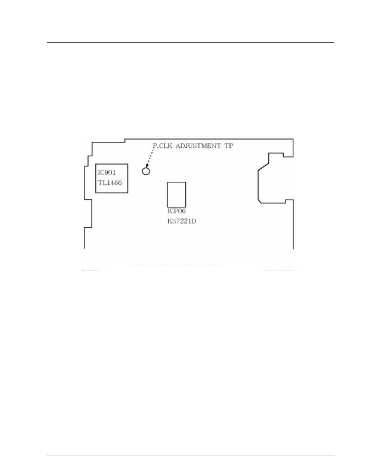
2. P. CLK Adjustment
1) “Camera”, no signal input.
2) P.CLK and AF MICOM.
3) Connect a frequency counter to P.CLK.
4) Press the “FADE(MODE UP)/BLC(MODE DOWN)” button so that the OSD state is
“004 XX XX”.
5) Adjust the “DSE(DATA UP)/TITLE(DATA DOWN)” button so that frequency is
.
PAL: NORMAL --> 9.453125MHz ± 50Hz. Hi8 --> 14.18750MHz ± 50Hz.
.
NTSC: NORMAL --> 9.534964MHz ± 50Hz. Hi8 --> 14.318182MHz ± 50Hz.
NOTE : Frequency changes after the confirm button is pressed.
Main PCB (Solder side)
3. Zoom VR Center
1) Camera “E-E”, 3100°K gray-scale chart.
2) Video(output) jack and EVR.
3) Connect monitor TV to video(output) jack.
4) Press the “FADE (MODE UP)/BLC
(MODE DOWN)” button so that the OSD state
is “OD6. ZVR.C XX XX”.
5) Press “PROGRAM AE(CONFIRM)” button.
6) Then, the microprocessor will work ;
- Find the Zoom VR Center position
- Store the data to mode 0B7.
4. Auto hall
1) Camera “E-E”, 3100°K gray-scale chart.
2) Video(output) jack and EVR.
3) Connect monitor TV to video(output) jack.
4) Press the “FADE(MODE UP)/BLC(MODE
DOWN)” button so that the OSD state is “OCD.
HALL XX XX”.
5) Press “PROGRAM AE(CONFIRM)” button.
6) Then, the microprocessor will work ;
- IRIS open, HALL maximum value found,
- IRIS closed, HALL minimum value found,
- IRIS open, HALL maximum value found,
- Store the data to mode 00A and mode 00B.
- Store the HALL min./max. data to mode 0C1
and mode 0C2.
Page 42
Samsung Electronics4-24
Alignment and Adjustment
5. AUTO IRIS
1) Camera “E-E”, 3100°K gray-scale chart.
2) Video(output) jack and AF MICOM.
3) Connect video(output) jack to waveform monitor input jack and monitor TV jack respectively.
4) Press the “FADE(MODE UP)/BLC(MODE
DOWN)” button so that the OSD state is “OCE.
IRIS XX XX”.
5) Press “PROGRAM AE(CONFIRM)” Button.
6) Then, the micro process will work;
- IRIS open, IRIS control minimum Value found.
- IRIS close, IRIS control minimum Value found.
- Store the data to mode 0B5, 0B6, 0C7 and 0C8.
7) The OSD shows “O.K”.
6. Auto white balance
1) Camera “E-E”, 3100°K/5100°K gray-scale chart.
2) Video(output) jack and AF MICOM.
4) Connect vectorscope input jack to video(output) jack.
3) Press the “FADE(MODE UP)/BLC(MODE
DOWN)” button so that the OSD state is “0CF.
AWB XX XX”.
a. W/B Indoor
a-1. Aim the camera at a 3100°K gray-scale chart
illuminated at 1500 to 2000 lx. (40us)
a-2. Press “PROGRAM AE(CONFIRM)” button so
that the white vector moves to the center
on screen of the vectorscope.
a-3. The OSD shows “OK!”.
b. W/B Outdoor
b-1. Aim the camera at a 5100°K gray-scale
(3100°K+CCB16) chart illuminated at 1500 to
2000 lx. (40us)
b-2. Press “PROGRAM AE(CONFIRM)” button
so that the white vector moves to the center
on screen of the vectorscope.
b-3. Store the data to mode 0C9, 0CA, 0CB and
0CC.
b-4. The OSD shows “OK!”.
7. Pre white balance (I)
1) Camera “E-E”, 3100°K gray-scale chart.
2) Video(output) jack and AF MICOM.
3) Connect vectorscope input jack to video(output) jack.
4) Press the “FADE(MODE UP)/BLC(MODE
DOWN)” button so that the OSD state is “137.
XX XX”.
5) Aim the camera at a 3100°K gray-scale chart
illuminated at 1500 to 2000 lx.
6) Adjust the “ DSE(DATA UP)/TITLE
(DATA DOWN)” button so that the white vector moves to the B-Y axial on screen of the
vectorscope.
Note : Bright dot shifts after the confirm button is
pressed.
Center of
white level
100IRE
Optical
black level
H
40US
Match the white luminance
point with the
black luminance
point
Match the white luminance
point with the
black luminance
point
Page 43
Samsung Electronics 4-25
Alignment and Adjustment
8. Pre white balance (II)
1) Camera “E-E”, 3100°K gray-scale chart.
2) Video(output) jack and AF MICOM.
4) Connect vectorscope input jack to video(output) jack.
3) Press the “FADE (MODE UP)/BLC(MODE
DOWN)” button so that the OSD state is “138.
XX XX”.
5) Aim the camera at a 3100°K gray-scale chart
illuminated at 1500 to 2000 lx.
6) Adjust the “DSE(DATA UP)/TITLE
(DATA DOWN)” button so that the white vector moves to the R-Y axial on screen of the vectorscope.
Note : Bright dot shifts after the confirm button is
pressed.
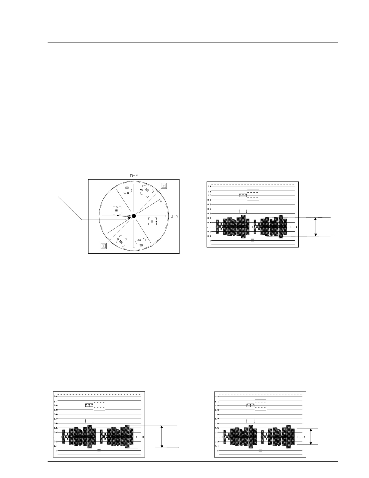
9 R-Y Positive Gain
1) Camera “E-E”, 3100°K color bar chart.
2) Video(output) jack and register of EEPROM.
3) Connect video(output) jack to waveform monitor input jack and monitor TV jack respectively.
4) Press the “FADE(MODE UP)/BLC(MODE
DOWN)” button so that the OSD state is “147.
XX XX”.
5) Aim the camera at a color bar chart illuminated
at 1500 to 2000 lx.
6) Adjust the “ DSE(DATAUP)/TITLE(DATA
DOWN)” button so that the red level is
70IRE(NTSC)/500mV(PAL) .
7) Be sure to press the “PROGRAM AE(CONFIRM)” button to memorize setting.
Note : Bright dot shifts after the confirm button is
pressed.
10. R-Y Negative Gain
1) Camera “E-E”, 3100°K color bar chart.
2) Video(output) jack and register of EEPROM.
3) Connect video(output) jack to waveform monitor input jack and monitor TV jack respectively.
4) Press the “FADE(MODE UP)/BLC(MODE
DOWN)” button so that the OSD state is “148.
XX XX”.
5) Aim the camera at a color bar chart illuminated
at 1500 to 2000 lx.
6) Adjust the “ DSE(DATAUP) /TITLE(DA TA
DOWN)” button so that the cyan level is
65IRE(NTSC)/350mV(PAL).
7) Be sure to press the “PROGRAM AE(CONFIRM)” button to memorize setting.
Note : Bright dot shifts after the confirm button is
pressed.
11. B-Y Positive Gain
1) Camera “E-E”, 3100°K color bar chart.
2) Video(output) jack and register of EEPROM.
3) Connect video(output) jack to waveform monitor input jack and monitor TV jack respectively.
4) Press the “FADE(MODE UP)/BLC(MODE
DOWN)” button so that the OSD state is “14B
XX XX”.
5) Aim the camera at a color bar chart illuminated
at 1500 to 2000 lx.
6) Adjust the “DSE(DATA UP)/TITLE (DATA
DOWN)” button so that the blue level is
50IRE(NTSC)/350mV(PAL).
7) Be sure to press the “PROGRAM AE(CONFIRM)” button to memorize setting.
Note : Bright dot shifts after the confirm button is
pressed.
Match the white luminance
point with the
black luminance
point
70IRE
65IRE
50IRE
Page 44
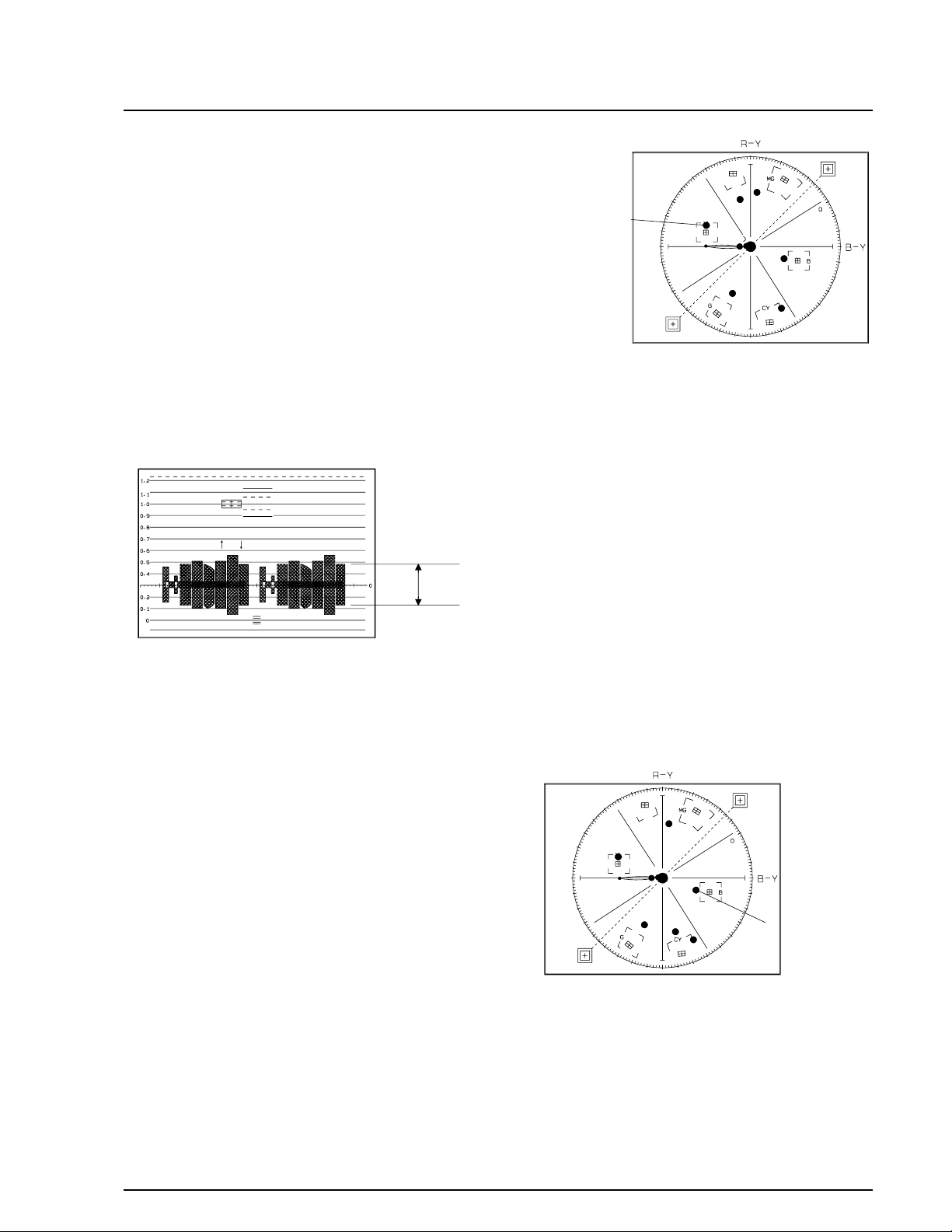
Samsung Electronics4-26
Alignment and Adjustment
12. B-Y Negative Gain
1) Camera “E-E”, 3100°K color bar chart.
2) Video(output) jack and register of EEPROM.
3) Connect video(output) jack to waveform monitor input jack and monitor TV jack respectively.
4) Press the “FADE(MODE UP)/BLC (MODE
DOWN)” button so that the OSD state is “14C
XX XX”.
5) Aim the camera at a color bar chart illuminated
at 1500 to 2000 lx.
6) Adjust the “DSE(DATA UP)/TITLE (DATA
DOWN)” button so that the yellow level is
50IRE(NTSC)/350mV(PAL).
7) Be sure to press the “PROGRAM AE(CONFIRM)” button to memorize setting.
Note : Bright dot shifts after the confirm button is
pressed.
13. R-Y Positive Hue
1) Camera “E-E”, 3100°K color bar chart.
2) Video(output) jack and register of EEPROM.
3) Connect video(output) jack to vectorscope
input jack and monitor TV jack respectively.
4) Press the “FADE(MODE UP)/BLC(MODE
DOWN)” button so that the OSD state is “149
XX XX”.
5) Aim the camera at a color bar chart illuminated
at 1500 to 2000 lx.
6) Adjust the “DSE(DATA UP)/TITLE
(DATA DOWN)” button so that the yellow vector is 165.
7) Be sure to press the “PROGRAM AE(CONFIRM)” button to memorize setting.
Note : Bright dot shifts after the confirm button is
pressed.
14. R-Y Negative Hue
1) Camera “E-E”, 3100°K color bar chart.
2) Video(output) jack and register of EEPROM.
3) Connect video(output) jack to vectorscope
input jack and monitor TV jack respectively.
4) Press the “FADE(MODE UP)/BLC(MODE
DOWN)” button so that the OSD state is “14A
XX XX”.
5) Aim the camera at a color bar chart illuminated
at 1500 to 2000 lx.
6) Adjust the “DSE(DATA UP)/TITLE
(DATA DOWN)” button so that the blue vector
is 346.
7) Be sure to press the “PROGRAM AE (CONFIRM)” button to memorize setting.
Note : Bright dot shifts after the confirm button is
pressed.
50IRE
YELLOW VECTOR
165 DEG
BLUE VECTOR
346 DEG.
Page 45
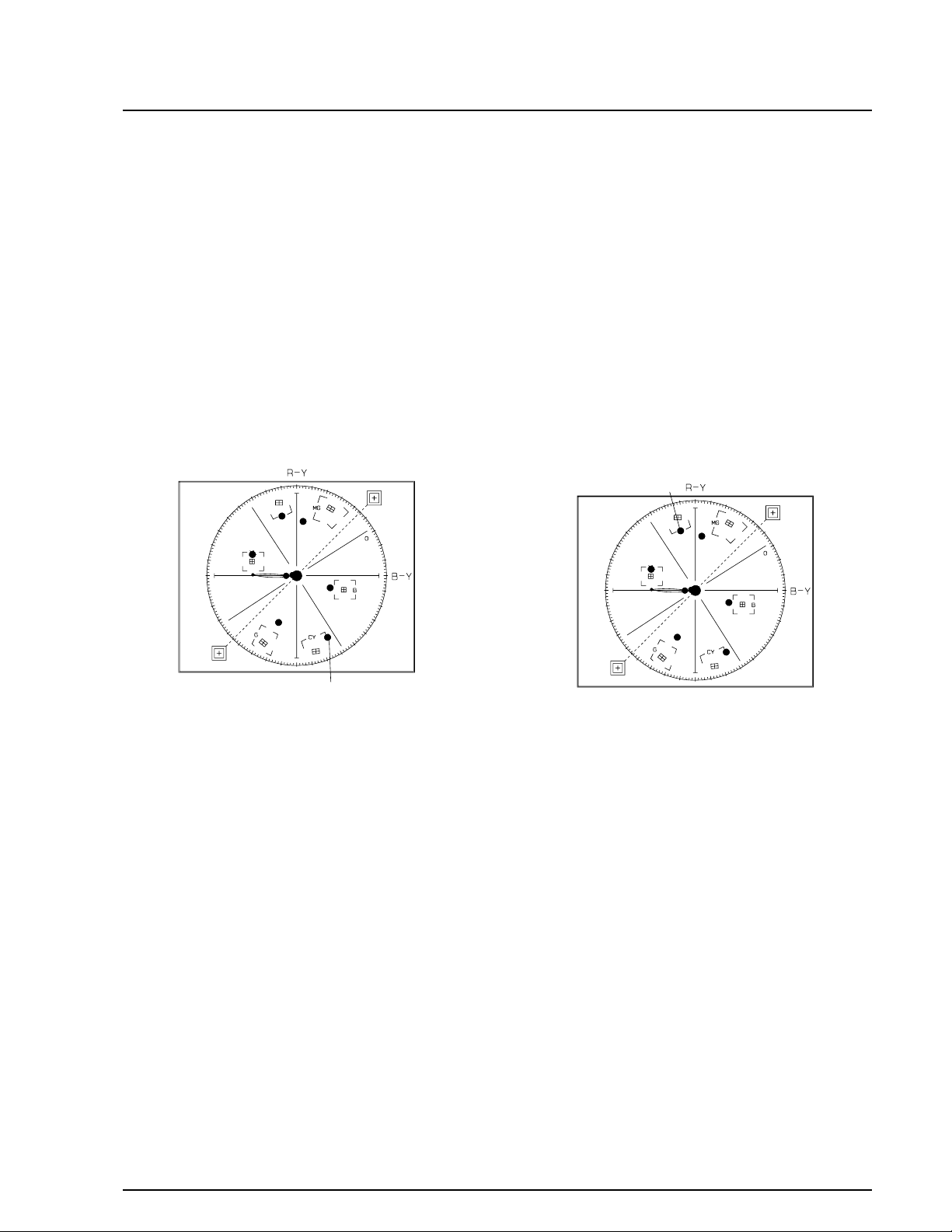
Samsung Electronics 4-27
Alignment and Adjustment
15. B-Y Positive Hue
1) Camera “E-E”, 3100°K color bar chart.
2) Video(output) jack and register of EEPROM.
3) Connect video(output) jack to vectorscope
input jack and monitor TV jack respectively.
4) Press the “FADE(MODE UP)/BLC(MODE
DOWN)” button so that the OSD state is “14D
XX XX”.
5) Aim the camera at a color bar chart illuminated
at 1500 to 2000 lx.
6) Adjust the “DSE(DATA UP)/TITLE
(DATA DOWN)” button so that the cyan
vector is 284.
7) Be sure to press the “PROGRAM AE (CONFIRM)” button to memorize setting.
Note : Bright dot shifts after the confirm button is
pressed.
16. B-Y Negative Hue
1) Camera “E-E”, 3100°K color bar chart.
2) Video(output) jack and register of EEPROM.
3) Connect video(output) jack to vectorscope
input jack and monitor TV jack respectively.
4) Press the “FADE(MODE UP)/BLC(MODE
DOWN)” button so that the OSD state is “14E
XX XX”.
5) Aim the camera at a color bar chart illuminated
at 1500 to 2000 lx.
6) Adjust the “DSE(DATA UP)/TITLE
(DATA DOWN)” button so that the red vector
is 104.
7) Be sure to press the “PROGRAM AE(CONFIRM)” button to memorize setting.
Note : Bright dot shifts after the confirm button is
pressed.
RED VECTOR
104 DEG.
CYAN VECTOR
284 DEG.
Page 46
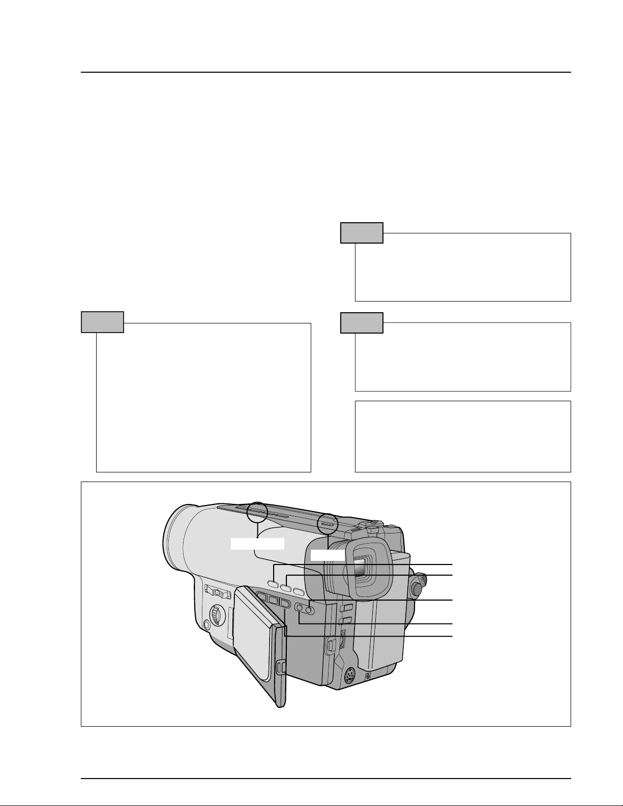
Samsung Electronics4-28
Alignment and Adjustment
4-2-3 CVF Adjustment
Notes :
1. After each adjustment step is completed, OSD shows “OK”.
2. EEPROM(ICV02) stores confirmed adjustment value of each adjustment step.
3. After finishing the adjustment, reset the main power source (OFF-ON) to memorize the adjustment data
in EEPROM.
4. Remote controller is used as a CVF adjust tool.
4-2-3 (a) PREPARATION
1. How to get into the CVF adjust mode.
Note : When XX XX is shown in service adjustment procedures, this indicates variable values.
1. Connect the power source (battery/DC
cable).
2. Set the mode switch of the camcorder to
“PLAYER” position.
3. Set OSD on state.
4. Press and hold the “EJECT” button and
“PLAY/STILL” button on the camcorder at
the same time for more than 5 seconds.
Then unit goes into service mode.
STEP2
MONITOR OSD shows “8. PLL EPR XX.
EVR XX”. Then CVF adjustment mode has
been activated successfully.
STEP3
8 PLL
EPR : XX EVR : XX
Short the two lands on the CVF PCB by solder to Ground. (They are displayed on page
4-31)
STEP1
EJECT
MODE DOWN
MODE UP
Confirm
DATA UP
DATA DOWN
PLAY/STILL
Page 47
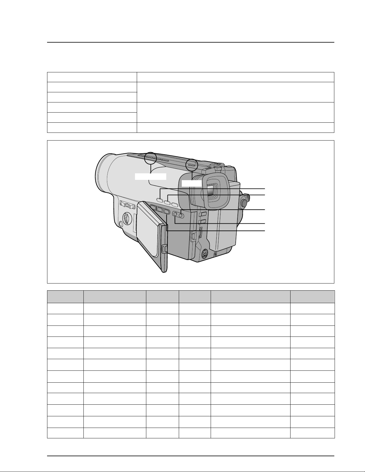
Samsung Electronics 4-29
Alignment and Adjustment
2. The following chart shows the function of each button. In service adjustment mode, button names are
different from those in customer camera function control mode. EX)ON/OFF button is the same as confirm.
NOTE : PLL --> BRIGHT --> R-SUB --> B-SUB --> COLOR --> TINT
Button
BLC(MODE DOWN)
FADE(MODE UP)
DSE(DATA UP)
TITLE(DATA DOWN)
PROGRAM AE(CONFIRM)
Function
When change the adjustment mode.
When change data value of adjust state.
Data store after finishing adjustment by “DATA UP/DATA DOWN” button
ADDRESS MODE NTSC PAL MEAN REMARK
0 TINT 88 65 TINT ADJUST
1 COLOR 65 75 COLOR GAIN ADJUST
2 BRIGHT 88 88 BRIGHT ADJUST
3 CONTRAST 60 60 CONTRAST FIXED
4 B SUB 8A 80 B-SUB ADJUST
5 R SUB 8A 80 R-SUB ADJUST
6 GAMMA 1 75 75 GAMMA1 GAIN FIXED
7 GAMMA 2 B1 B1 GAMMA2 GAIN FIXED
8 PLL 60 60 PLL ADJUST
9 MODE 1 02 0E PAL/NTSC FIXED
A MODE 2 00 00 NORMAL/TEST FIXED
B MODE 3 F5 F5 HD-POSITION FIXED
EJECT
MODE DOWN
MODE UP
Confirm
DATA UP
DATA DOWN
PLAY/STILL
Page 48
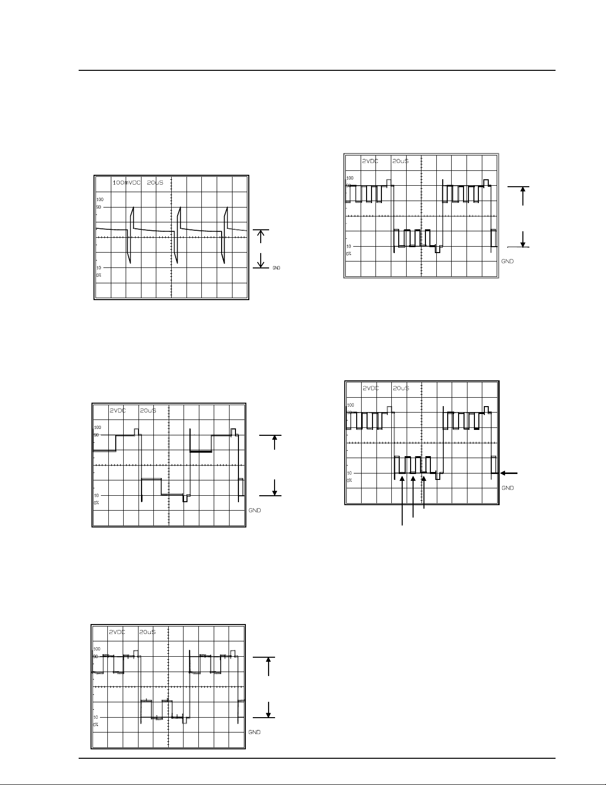
Samsung Electronics4-30
Alignment and Adjustment
4. B-Sub Brightness (ADDRESS : 5.B-SUB)
1) Connect an oscilloscope probe to TP-B.
2) Adjust the EVR so that B OUT(Blue) level is
8.0Vp-p (pedestal to pedestal).
5. Color(ADDRESS : 1.COLOR)
1) Connect an oscilloscope probe to TP-B.
2) Adjust the EVR so that the Yellow level is equal
to the pedestal line.
8.0V
(PEDESTAL TO
PEDESTAL)
4-2-3 (b) ADJUSTMENT
1. PLL (ADDRESS : 8.PLL)
1) Connect an multimeter probe to TP-P
2) Adjust the EVR so that DC voltage is
DC1.8±0.05Vp-p.
2. Brightness (ADDRESS : 2.BRIGHT)
1) Connect an oscilloscope probe to TP-G.
2) Adjust EVR so that bright(Green) level is
8.0V±0.1Vp-p (pedestal to pedestal).
3. R-Sub Brightness (ADDRESS : 4.R-SUB)
1) Connect an oscilloscope probe to TP-R
2) Adjust the EVR so that R-OUT(Red) level is
8.0Vp-p (pedestal to pedestal).
1.8V
8.0V
(PEDESTAL TO
PEDESTAL)
8.0V
(PEDESTAL TO
PEDESTAL)
YELLOW LEVEL
PEDESTAL
LINE
GREEN LEVEL
RED LEVEL
Page 49
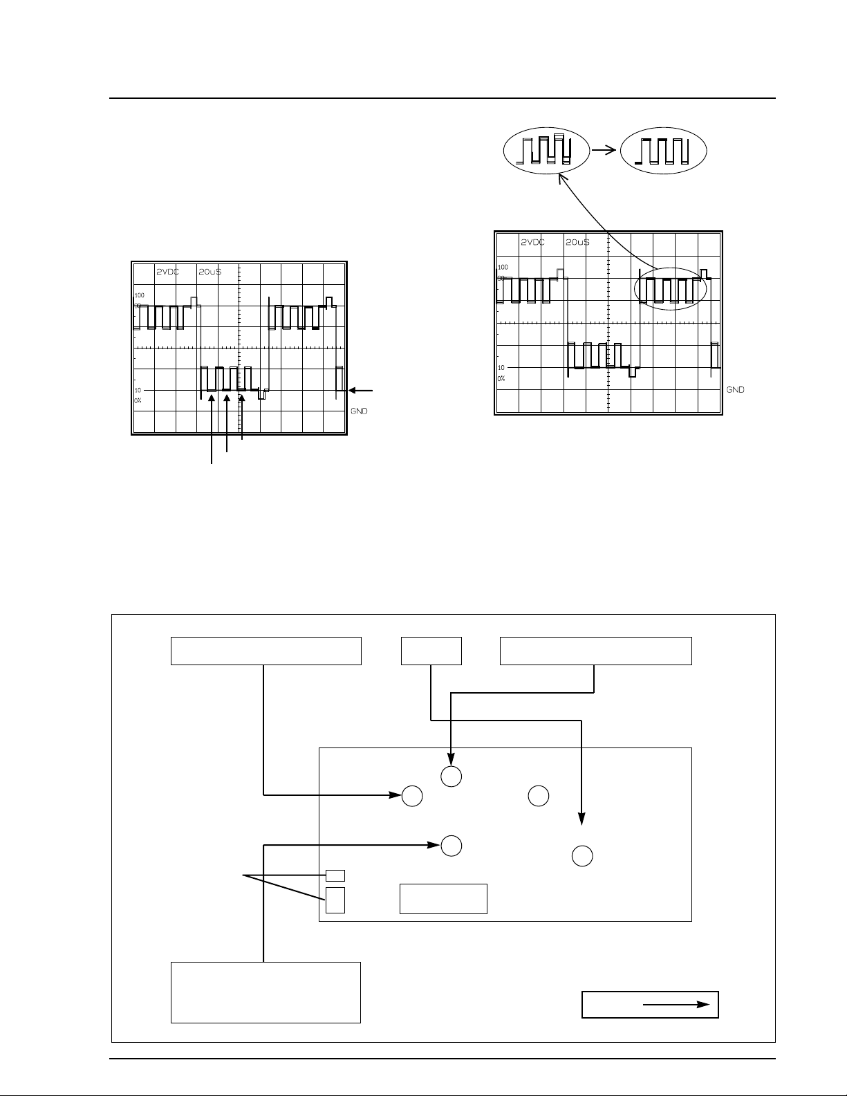
Samsung Electronics 4-31
Alignment and Adjustment
6. TINT(ADDRESS : 0.TINT)
1) Connect an oscilloscope probe to TP-B.
2) Adjust the EVR so that the dual waveforms are
superimposed.(PAL MODEL)
3) Adjust the EVR so that the bright(Green) level
is equal to the Red level.(NTSC MODEL)
DUAL WAVEFORMS ARE SUPERIMPOSED.
ADJ. point
1. PLL 3. R-SUB BRIGHTNESS2. BRIGHTNESS
10P CON
4. B-SUB BRIGHTNESS
5. COLOR
6. HUE
Note : When adjusting CVF be sure to short cir-
cuit between Ground and “A”part to store
the confirmed data in EEPROM when
pushing ON/OFF button.
A
GND
G
R
B
P
L
CVF Adjust Mode
(Short)
YELLOW LEVEL
PEDESTAL
LINE
GREEN LEVEL
RED LEVEL
Page 50

Samsung Electronics4-32
Alignment and Adjustment
4-2-4 EVF Adjustment
Notes :
1. For EVF adjustment, use the buttons on set and remote controller.
2. After each adjustment step is completed, OSD shows “OK”.
3. EEPROM(ICV02) stores confirmed adjustment value of each adjustment step.
4. After finishing the adjustment, turn power off.
4-2-4 (a) PREPARATION
1. How to get into the EVF adjust mode.
Notes : When XX XX is shown in service adjustment procedures, this indicates variable values.
1. Connect the power source (battery/DC
cable).
2. Set the mode switch of the camcorder to
“PLAYER” position.
3. Connecting the AV JACK of the camcorder
to monitor makes OSD appear.
STEP1
Monitor OSD shows “0 USER BRT EPR XX.
EVR XX”. Then EVF adjustment mode has
been activated successfully.
0 USER BRT.
EPR : XX EVR : XX
Press and hold the “EJECT” button and
“PLAY/STILL” button on the camcorder at
the same time for more than 5 seconds.
STEP2
Notes : "XX" indicates variable values.
EJECT
MODE DOWN
MODE UP
Confirm
DATA UP
DATA DOWN
PLAY/STILL
Page 51
Samsung Electronics 4-33
Alignment and Adjustment
2. The following chart shows the function of each button.
Button
BLC(MODE DOWN)
FADE(MODE UP)
DSE(DATA UP)
TITLE(DATA DOWN)
PROGRAM AE(CONFIRM)
Function
When change the adjustment mode.
When change data value of adjust state.
Data store after finishing adjustment by “DATA UP/DATA DOWN” button
ADDRESS MODE NTSC PAL MEAN REMARK
0 USER BRHT 4B 4B BRIGHT ADJUST
1 S SUB R 80 80 R-SUB BRHT FIXED
2 R SUB B 80 80 B-SUB BRHT FIXED
3 CONTRAST 88 88 CONTRAST ADJUST
4 S CONT R 99 99 R-SUB CONT FIXED
5 S CONT B 99 99 B-SUB CONT FIXED
6 GAMMA 2 70 70 GAMMA 2 FIXED
7 GAMMA 1 92 92 GAMMA 1 FIXED
8 ONLY 0 00 00 ONLY 00 FIXED
9 COM DC 7A 7A VCOM ADJUST
A COLOR 80 80 COLOR FIXED
B HUE 80 80 TINT FIXED
C W/B LMT 1B 1B W/B LIMIT FIXED
D FIL/LPF 00 00 FIL/LPF FIXED
E PIC/GAIN 00 00 PICTURE/GAIN FIXED
F MODE/PLL 0C 0C MODE/PLL ADJUST
10 SYNC GEN 00 00 SYNC GEN FIXED
11 Y MIRROR 00 01 NTSC/PAL FIXED
12 OUT INV 00 00 OUT INV FIXED
13 X MIRROR 00 00 UP/DOWN FIXED
14 H POSI 10 10 H-POSITION FIXED
15 HDO OUT 00 00 HDO OUT FIXED
Notes : In service adjustment mode, button names are different from those in customer function control
mode.
3. Adjustment mode table
Page 52

Samsung Electronics4-34
Alignment and Adjustment
4. CONTRAST
1) TP-B & EVR
2) Connect an oscilloscope probe to TP-B.
3) Adjust the EVR so that A level is 2.0Vp-p .
4-2-4 (b) ADJUSTMENT
1. PLL
1) TP-P & EVR
1) Connect an voltmeter to TP-P
2) Adjust the EVR so that DC voltage is
DC1.6±0.2Vp-p.
2. VCOM
1) TP-L & EVR
2) Connect an voltmeter to TP-L.
3) Adjust the EVR so that DC voltage is
5.6±0.05Vp-p (pedestal to pedestal).
3. BRIGHTNESS
1) TP-G & EVR
2) Connect an oscilloscope probe to TP-G.
3) Adjust the EVR so that bright level is 8.0Vp-p
(pedestal to pedestal).
10P CON
A
GND
G
R
B
P
L
EVF Adjust Mode
(Short)
Note : When adjusting EVF be sure to short circuit between Ground and “A”part to store
the confirmed data in EEPROM when pushing ON/OFF button.
After finishing the adjustment, you have to reset.
PEDISTAL
TO PEDISTAL
A
Page 53

Samsung Electronics 4-35
Alignment and Adjustment
Notes: For LCD adjustment, use the buttons on the video camera and the remote control.
After each adjustment step is completed, OSD shows "OK".
EEPROM(ICL202) stores confirmed adjustment value of each adjustment step.
After finishing the adjustment, turn power off.
4-2-5 (a) PREPARATION
1. How to get into the LCD adjust mode.
When monitor OSD shows as above screen, LCD
adjustment mode has been activated successfully.
Note : "XX" indicates variable values.
Monitor screen
Remote Control Button Location
VCO
EPR:XX EVR:XX
A.
4-2-5 LCD Adjustment
1. Remove the lithum battery from camcorder.
2. Connect the power source (battery/DC
cable).
3. Set the mode switch of the camcorder to
“PLAYER” position.
4. Camera screen and OSD appears.
STEP1
Press and hold the “EJECT” button and “FF”
button on the camcorder at the same time for
more than 5 seconds.
STEP2
EJECT
MODE DOWN
MODE UP
Confirm
DATA UP
DATA DOWN
FF
Page 54

Samsung Electronics4-36
Alignment and Adjustment
*
The adjustment sequence is VCO->VCOM->BRIGHT->R-SUB->B-SUB->COLOR->TINT.
Note: In service adjustment mode, button names are different from those in customer function control
mode.
2. Functions of each button on the Remote Control
Button
BLC(MODE DOWN)
FADE(MODE UP)
DSE(DATA UP)
TITLE(DATA DOWN)
PROGRAM AE(CONFIRM)
Function
When changing the adjustment mode.
When changing data value of adjust state.
Store data after finishing adjustment by “DATA UP/DATA DOWN” button.
ADDRESS MODE NTSC PAL MEAN REMARK
01 VCO A0 C0 PLL Adjust
02 VCOM 89 89 COMMON Adjust
03 BRIGHT 97 97 BRIGHT Adjust
04 R-SUB A7 A7 R-SUB CONT Adjust
05 B-SUB A4 A4 B-SUB CONT Adjust
06 COLOR 80 8E COLOR Adjust
07 TINT 00 8E TINT Adjust NTSC only
08 CONTRAST 96 96 CONTRAST Fix initial value
09 GAMMA 82 82 GAMMA Fix initial value
0A LED CONTROL FF FF LED control when powered
0B BRIGHT MIN 01 01 Bright variation of MIN direction for USER
0C BRIGHT MAX 01 01 Bright variation of MAX direction for USER
0D COLOR MIN 02 05 Color variation of MIN direction for USER
0E COLOR MAX 02 06 Color variation of MAX direction for USER
0F TINT MIN 00 06 Tint variation of MIN direction for USER
10 TINT MAX 00 04 Tint variation of MAX direction for USER
11 CHECK1 19 19 CHECK1 Fix initial value
12 CHECK2 20 20 CHECK2 Fix initial value
3. Adjustment mode table
Page 55
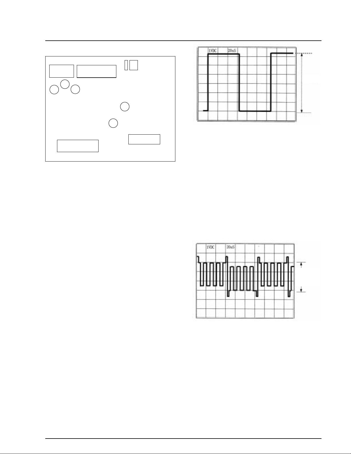
Samsung Electronics 4-37
Alignment and Adjustment
X-T AL
24P-LCD
10P-BL
A
G
B
VCO
VCOM
R
1. VCO
1) TP-VCO & EVR
2) Connect an voltmeter to TP-VCO.
3) Adjust the EVR so that DC voltage is DC
1.6±0.05 V.
2. VCOM
1) TP-COM & EVR
2) Connect an voltmeter to TP-COM.
3) Adjust the EVR so that DC voltage is DC
1.45±0.05 V.
3. Brightness
1) TP-COM & EVR
2) Connect an oscilloscope probe to TP-COM.
3) Adjust the EVR so that level is 6.4±0.1 Vp-p.
Note: In LCD adjustment mode, when shorting
"A" of PCB to GND and pressing the
START/STOP button. Store in EEPROM.
Reset after adjustment is complete.
4. R-Sub Brightness
1) TP-R & EVR
2) Connect an oscilloscope probe to TP-R.
3) Adjust the EVR so that pedestal level is equal to
TP-G level.
5. B-Sub Brightness
1) TP-B & EVR
2) Connect an oscilloscope probe to TP-B.
3) Adjust the EVR so that pedestal level is equal to
TP-G level.
6. Color
a) TP-B & EVR
b) Connect an oscilloscope probe to TP-B.
c) Adjust the EVR so that yellow level is equal to
pedestal level.
LEVEL
(PEDESTAL
TO
PEDESTAL)
4-2-4 (b) Adjustment
4. Location of Adjustment TP
6.4Vp-p
14P
Page 56

Samsung Electronics4-38
Alignment and Adjustment
7. Tint (NTSC only)
a) TP-B & EVR
b) Connect an oscilloscope probe to TP-B.
c) Adjust the EVR so that green level is equal to
red level.
8. C-COM (PAL only)
a) TP-B & LL205
b) Connect an oscilloscope probe to TP-B.
c) Adjust the EVR so that red carrier level is mini-
mized.
Page 57

Samsung Electronics 4-39
Alignment and Adjustment
1. Equipment :
1) Monitor TV.
2) Dual trace oscilloscope of over 20MHz band,
incorporates delay mode.
(Use 10 : 1 probe unless otherwise specified.)
3) Frequency counter
4) DC power supply.
5) Alignment tape (Colour bar : SP)
6) 8mm Video Tape for record.
2. Composition of VCR P.C.Boards
1) Main PCB (DC/DC connector, system control,
servo, video, audio, camera)
2) Rear PCB
3) Function PCB
4) Front PCB
3. How to get into service “ADJUST” mode.
4-3. VCR Section Adjustment
1. Connect the power source (battery/DC cable).
2. Set the power switch of the camcorder to
PLAYER position.
3. Press the eject key to eject mode.
STEP 1
1. Press and hold “STOP(DATE/TIME)” button
on the Camcorder and “EJECT” button on
the Camcorder at the same time for more
than 5 seconds.
2. If the color bar generated internally appears
on the monitor and adjustment mode displayed like the figure below, VCR adjustment mode has been successfully activated.
3. Insert tape into housing ass’y and then perform the adjustments.
STEP 2
01.MODEL CODE0
EPR:XX EVR:XX
TV or LCD/EVF monitor
Address of the adjustment mode.
: there are 01H to 1CH.(refer to adjustment table on the page 4-42)
Name of the adjustment mode.
: every address have a name like this (refer
to adjustment table on the page 4-42)
Present data
: be adjusted before.
New data
: be adjusted newly.
4-3-1 Preparations
Page 58

Samsung Electronics4-40
Alignment and Adjustment
4. The location of function button.
5. If you want to finish the adjustment mode, you have to do Battery Reset.
The Battery Reset means that you pull out the power source and pull in it again.
Then, the adjustment ended and the camcorder works normally.
Note : In service adjustment mode, button name are different
from those in customer function control mode.
EX) “PROGRAM AE ” button is the same as CONFIRM.
EJECT
MODE DOWN
MODE UP
Confirm
DATA UP
DATA DOWN
DATE/TIME
Page 59
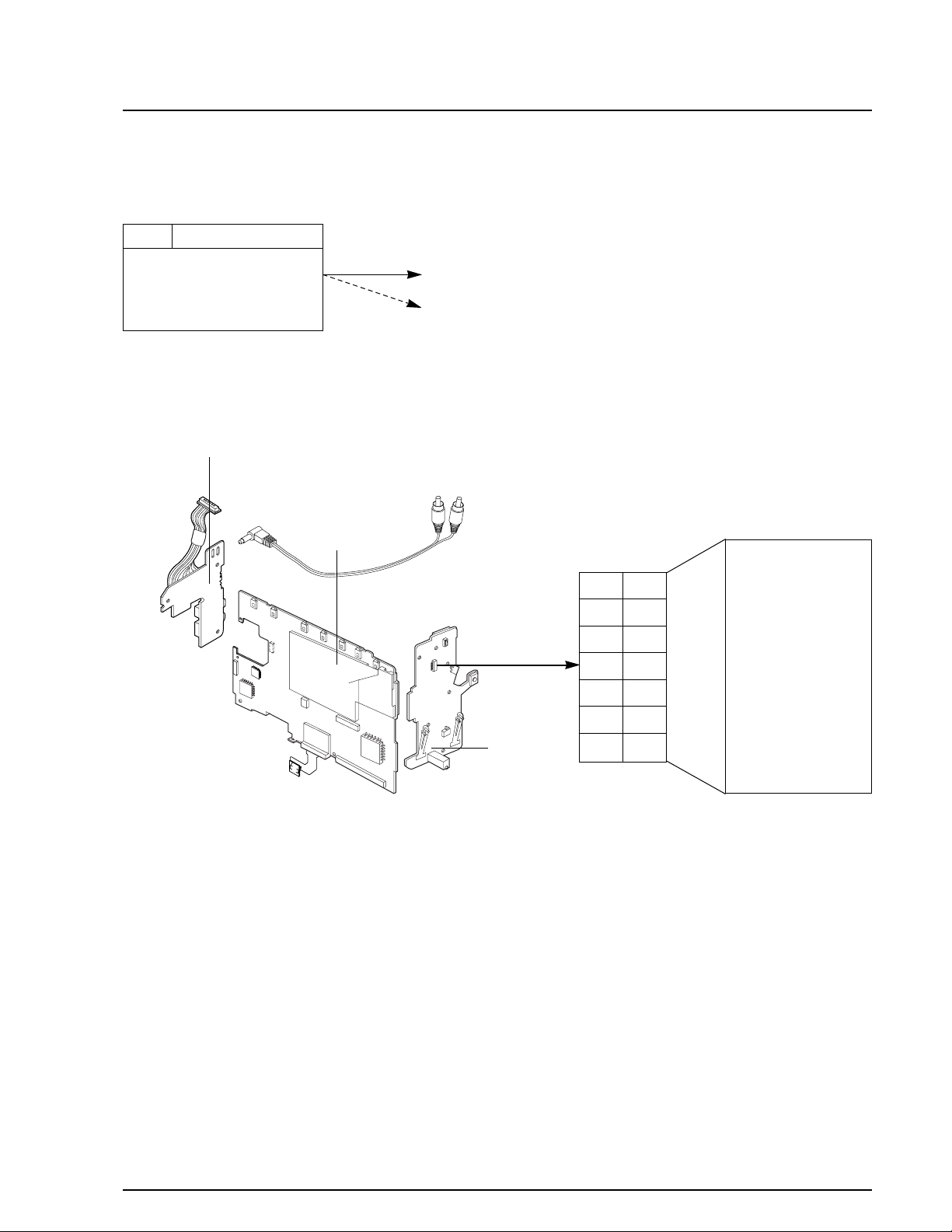
Samsung Electronics 4-41
Alignment and Adjustment
Note 2 : How to connect video out signal.
-Connect the video cable to ass’y A/V Jack.
Note 3 : How to record -1. Insert a recordable tape.
-2. Press the SW474 (START/STOP) button on the Rear board in the adjustment
mode.
4-3-2 VCR Section
Note 1 : From this point forward, the structure of every adjustment is as follows.
Test point
Step Adjustment Item
1. Mode and input signal/
alignment tape
2. Test point and ADJ. part
3. Result and Remarks
ADJ. point
Fig. 1 Video Signal Connection
MAIN PCB
REAR PCB
FRONT PCB
13
VIDEO OUT
12
11
10
9
8
7
6
5
4
3
2
1
NC
PB RF
AUDIO OUT
HD SW
VCR UNREG
JIG CS
VCR UNREG
JIG SCK
SS GND
JIG SO
JIG DETECT
JIG SI
AUDIO GND
14
CN452
14 13
12 11
10 9
87
65
43
21
Page 60
Samsung Electronics4-42
Alignment and Adjustment
4-3-3 Adjustment
1. Kinds of adjustment
2. Adjustment
* Please keep the order according to explanation.
2-1. Model Code 0
a. Preparation
ADDRESS NAME
NORMAL MODEL HI 8 MODEL
NTSC PAL NTSC PAL
01
02
MODEL CODE0
Model code setting
Model code setting
Adjustment
03
MODEL CODE1
04
HD SWP
05
COLOR BAR LEVEL
06
Y-EMPHASIS IN (NOR)
Adjustment
07
PB OUT-LEVEL (NOR)
Adjustment
08
Y-EMPHASIS IN (HI8)
- - Adjustment
09
PB OUT LEVEL (HI8)
- - Adjustment
0A
VIDEO OUT LEVEL
Adjustment
0B
Y-FM CARRIER (NOR)
Adjustment
0C
Y-FM DEVIAT (NOR)
Adjustment
0D
Y-FM CARRIER (HI8)
- - Adjustment
0E
Y-FM DEVIAT (HI8)
- - Adjustment
0F
AUDIO BPF-ADJ
Adjustment
10
C-EMPHASIS
CD CD A9 CD
11
WHITE CLIP (NOR)
80 80 80 80
12
REC C LEVEL
B0 99 C0 D0
13
REC Y FM LEVEL
C9 C9 A8 A8
14
PB DEL ADJ
15
D CLIP (NOR)
16
DEL ADJ
17
SMEAR CONT
18
MTQ (PB)
19
MTF0 (NOR)
1A
WHITE CLIP (HI8)
1B
MTF0 (HI8)
1C
D CLIP (HI8)
1D
1E
1F
MODEL CODE
TITLE LANGUAGE
HD SWP (SUB DATA)
BATTERY END LEVEL
8B 8B 8B 8B
- - D0 D0
- - 7A 7A
- - 60 55
- - 9A 9A
- - 8E 8E
----
0C 0C 0C 0C
91 91 91 91
65 65 85 85
65 65 65 65
85 65 85 85
99 99 90 90
1C
ATF REF.
-
-
--
----
TAPE NONE
POWER SOURCE
NONE
NONE
01
MODEL CODE0
EQUIPMENT
OTHER
TEST POINT
ADDRESS
NAME
Page 61
Samsung Electronics 4-43
Alignment and Adjustment
2-3. Head Switching Point
: This adjustment is performed after the
replacement of deck mechanism.
• Without this adjustment, there will be a noise
in playback picture.
a. Preparations
b. Connect a power source.
c. Get into the VCR adjustment mode.
d. Press the “FADE(MODE UP)” or “BLC(MODE
DOWN)” button of FUNCTION so as to select
the address 03.
e. Insert the Standard Color Bar Tape and press
the “PLAY” button.
Note : If there is no video out, when you pressed
the “PLAY” button, you can not adjust the
Head Switching Point.
It may be caused by maladjusted VIDEO
block.
In this case, adjust the VIDEO block before
the Head Switching Point.
VIDEO block adjustments are 2-3~2-11.
f. The data of Head Switch is set to 7.2H~7.7H
automatically.
g. Be sure to press the “PROGRAM AE(CON-
FIRM)” button on FUNCTION to memorize setting.
h. Reset the power source so as to fix the new data
to the camcorder’s EEPROM.
b. Connect a power source.
c. Get into the VCR adjustment mode.
d. Press the “FADE(MODE UP)” or
“BLC(MODE DOWN)” button of FUNCTION
so as to select the address 01.
e. Press the “TILTLE(DATA DOWN)/ DSE(DATA
UP)” so that OSD shows“ ”ERR:XX EVR: XX”
“XX” is different dependent on the model as
below.
f. Be sure to press the “PROGRAM AE(CON-
FIRM)” button on FUNCTION to memorize setting.
g. Reset the power source so as to fix the new data
to the camcorder’s EEPROM.
2-2. Model Code 1
a. Preparation
b. Connect a power source.
c. Get into the VCR adjustment mode.
d. Press the “FADE(MODE UP)” or
“BLC(MODE DOWN)” button of FUNCTION
so as to select the address 02.
e. Press the “TITLE(DATA DOWN)/ DSE(DATA
UP)” so that OSD shows“ ”ERR:XX EVR: XX”
“XX” is different dependent on the model as
below.
f. Be sure to press the “PROGRAM AE(CON-
FIRM)” button on FUNCTION to memorize setting.
g. Reset the power source so as to fix the new data
to the camcorder’s EEPROM.
TAPE
STANDARD COLOR BAR TAPE
RECORDED WITH SP SPEED
POWER SOURCE
NONE
NONE
03
HD SWP
EQUIPMENT
OTHER
TEST POINT
ADDRESS
NAME
03.HD SW P
EPR : XX EVR : YY
7.5H
Model Name
VP-L500
VP-L520
VP-L530
VP-L530B
VP-L550
Addressed code
02
02
33
33
77
Model Name
SCL500
SCL520
SCL530
SCL550
Addressed code
02
02
73
77
Model Name
VP-L500
VP-L520
VP-L530
VP-L530B
VP-L550
Addressed code
A4
E4
E4
E4
E4
Model Name
SCL500
SCL520
SCL530
SCL550
Addressed code
A2
A4
E4
E4
Page 62

Samsung Electronics4-44
Alignment and Adjustment
2-4. Adjusting Y-Emphasis Input (NORMAL)
: This adjustment is performed to set the Y level
which is recorded in tape.
Maladjusted Y level impact to the next adjustment.
a. Preparations
b. Connect a power source.
c. Get into the VCR adjustment mode.
d. Press the “FADE(MODE UP)” or “BLC(MODE
DOWN)” button of FUNCTION so as to select
the address 05.
e. Insert a Normal Tape to the camcorder.
f. Connect the oscilloscope to the addressed Test
Point.
g. Press the “TITLE(DATA DOWN)/DSE(DATA
UP)” button so that the IC201 PIN13 is
0.5±0.02Vp-p from SYNC tip to peak level.
h. Be sure to press the “PROGRAM AE(CON-
FIRM)” button on FUNCTION to memorize
setting.
i. Reset the power source so as to fix the new data
to the EEPROM.
2-5. PB OUT LEVEL (NORMAL)
(Hi8 NORMAL PLAY BACK)
(NOMAL PLAY BACK OF Hi8 SET)
: This adjustment is perform to set the A/D
input level to the regulated level.
a. Preparations
b. Connect a power source.
c. Get into the VCR adjustment mode.
d. Press the “FADE(MODE UP)” or
“BLC(MODE DOWN)” button of FUNCTION
so as to select the address 06.
e. Insert the Standard Color Bar Tape and press
the “PLAY” button.
f. Connect the oscilloscope to the addressed Test
Point.
g. Press the “TITLE(DATA DOWN)/DSE(DATA
UP)” button so that the Q272 Emitter is
0.9±0.02Vp-p from SYNC to peak level.
h. Be sure to press the “PROGRAM AE(CON-
FIRM)” button on FUNCTION to memorize
setting.
i. Reset the power source so as to fix the new data
to the camcorder’s EEPROM.
2-6. Y-EMPHASIS INPUT (HI8)
a. Preparations
b. Connect a power source.
c. Get into the VCR adjustment mode.
TAPE
STANDARD COLOR BAR TAPE
RECORDED WITH SP SPEED
OSCILLOSCOPE
Q272 EMITTER
06
PB OUT-LEVEL (NOR)
EQUIPMENT
TEST POINT
ADDRESS
NAME
0.5 0.02Vp-p
TAPE HI8 TAPE
OSCILLOSCOPE
NONE
IC201 PIN13
07
Y-EMPHASIS IN (HI8)
EQUIPMENT
OTHER
TEST POINT
ADDRESS
NAME
R248 (Hi8 : NORMAL PLAYBACK)
OSCILLOSCOPE
IC 201 PIN 13
05
Y-EMPHASIS IN (NOR)
EQUIPMENT
OTHER
TEST POINT
ADDRESS
NAME
8MM (NORMAL) TAPETAPE
0.9 0.02Vp-p
Page 63
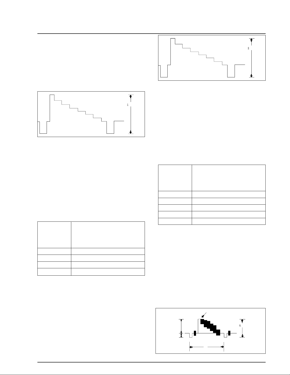
d. Press the “FADE(MODE UP)” or
“BLC(MODE DOWN)” button of FUNCTION
so as to select the address 07.
e. Insert the Hi-8 tape to the camcorder
f. Connect the oscilloscope to the addressed Test
Point.
g. “TITLE(DATA DOWN)/DSE(DATA UP)” but-
ton so that the IC201 PIN13 is 0.5±0.02Vp-p
from SYNC tip to peak level.
h. Be sure to press the “PROGRAM AE(CON-
FIRM)” button on FUNCTION to memorize
setting.
i. Reset the power source so as to fix the new data
to the camcorder’s EEPROM.
2-7. PB Output Level (Hi8)
: This adjustment is performed to set the A/D
input level to the regulated level.
a. Preparations
b. Connect a power source.
c. Get into the VCR adjustment mode.
d. Press the “FADE(MODE UP)” or “BLC (MODE
DOWN)” button of FUNCTION so as to select
the address 08.
e. Insert a Hi-8 standard color bar tape and press
the PLAY button.
f. Connect the oscilloscope counter to the
addressed Test Point.
g. Press the “TITLE(DATA DOWN)/DSE(DATA
UP)” button so that the CN452 PIN13 is
0.9±0.02Vp-p from SYNC to peak level.
h. Be sure to press the “PROGRAM AE(CON-
FIRM)” button on FUNCTION to memorize
setting.
i. Reset the power source so as to fix the new data
to the camcorder’s EEPROM.
2-8. VIDEO Out Level
: This adjustment is performed to set the VIDEO
out level to the regulated level.
a. Preparations
b. Connect a power source.
c. Get into the VCR adjustment mode.
d. Press the “FADE(MODE UP)” “BLC (MODE
DOWN)” button of FUNCTION so as to select
the address 09.
e. Insert a standard color bar tape and press the
PLAY button.
f. Connect the oscilloscope counter to the
addressed Test Point.
g. Press the “TITLE(DATA DOWN)/DSE(DATA
UP)” button so that the CN452 PIN13 is
1.0±0.02Vp-p from SYNC to peak level.
Samsung Electronics 4-45
Alignment and Adjustment
0.5 0.02Vp-p
TAPE
STANDARD COLOR BAR TAPE
RECORDED WITH SP SPEED
OSCILLOSCOPE
R248
06
PB OUT-LEVEL (NOR)
EQUIPMENT
TEST POINT
ADDRESS
NAME
0.9 0.02Vp-p
TAPE
STANDARD COLOR BAR TAPE
RECORDED WITH SP SPEED
OSCILLOSCOPE
CONNET THE MOINTER(75Ω)
CN452 PIN13
09
VIDEO OUT LEVEL
EQUIPMENT
OTHER
TEST POINT
ADDRESS
NAME
APPROX.
0.7V
APPROX.
0.3V
WHITE ( APPROX. 100% )
H
1.0 0.02Vp-p
Page 64
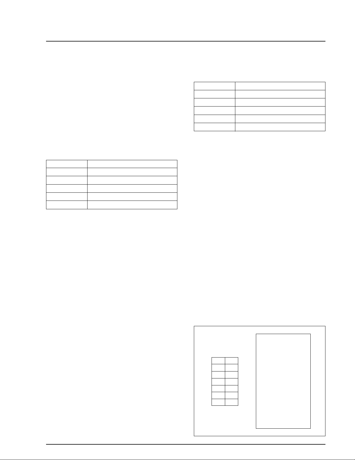
though the adjustment is performed in VCR
record mode.
So you have to do it carefully.
a. Preparations
b. Connect a power source.
c. Get into the VCR adjustment mode.
d. Press the “FADE(MODE UP)” or “BLC(MODE
DOWN)” button of FUNCTION so as to select
the address 0B.
e. Insert a NORMAL Tape to the camcorder.
f. Press the “START/STOP” button on the Rear
board so as to set the camcorder to RECORDING mode.
g. Record for enough time to check the waveform
when you playback where you recorded in
step f).
* 1 minute may be enough to check the waveform
in playback mode.
h. Connect the oscilloscope to the addressed Test
Point.
i. Make sure that the waveform is to be as typical
wave form on the next page.
(If OK, go to step l).
j. In case of the waveform level is bigger than
1Vp-p, press the Data Down button so as to set
to down the waveform level and if the waveform level smaller than 1Vp-p, press the Data
Up button so as to set to up the waveform level.
k. Repeat step g), h), i).
14
12
10
8
6
4
2
13
11
9
7
5
3
1
13
VIDEO OUT
12
11
10
9
8
7
6
5
4
3
2
1
NC
PB RF
AUDIO OUT
HD SW
VCR UNREG
JIG CS
VCR UNREG
JIG SCK
SS GND
JIG SO
JIG DETECT
JIG SI
VIDEO GND
14
CN452
h. Be sure to press the “PROGRAM AE(CON-
FIRM)” button on FUNCTION to memorize
setting.
i. Reset the power source so as to fix the new data
to the camcorder’s EEPROM.
2-9. Y-FM Carrier (NOR)
: This adjustment is performed to set the sync-
tip level of the composite video signal.
Maladjusted Y-FM carrier impact to the playback picture, there may be black or white dot
noise.
a. Preparations
b. Connect a power source.
c. Get into the VCR adjustment mode.
d. Press the “FADE(MODE UP)” “BLC (MODE
DOWN)” button of FUNCTION so as to select
the address 0A.
e. Insert a Normal Tape to the camcorder.
f. Press the “START/STOP” button on the Rear
board so as to set the camcorder to RECORD-
ING mode.
g. Connect the frequency counter to the addressed
Test Point.
h. Press the “TITLE(DATA DOWN)/ DSE(DATA
UP)” button so as to set the frequency to
4.38MHz±0.02MHz.
i. Be sure to press the “PROGRAM AE(CON-
FIRM)” button of FUNCTION to memorize setting.
j. Reset the power source so as to fix the new data
to the camcorder’s EEPROM.
2-10. Y-FM DEVIATION (NOR)
: This adjustment sets the Y-FM modulation
level in recording. For adjustment, playback
the self-recorded signal and observe the
VIDEO OUT signal.
* Note : It is a little difficult to adjust because you
can check the waveform in playback mode even
Samsung Electronics4-46
Alignment and Adjustment
TAPE NORMAL TAPE FOR RECORDING
OSCILLOSCOPE
NONE
IC201 PIN41
0A
Y-FM CARRIER (NOR)
EQUIPMENT
OTHER
TEST POINT
ADDRESS
NAME
TAPE NORMAL TAPE FOR RECORDING
OSCILLOSCOPE
NONE
CN452 PIN13
0B
Y-FM DEVIAT (NOR)
EQUIPMENT
OTHER
TEST POINT
ADDRESS
NAME
Page 65

Samsung Electronics 4-47
Alignment and Adjustment
l. Be sure to press the “PROGRAM AE(CON-
FIRM)” button on FUNCTION to memorize setting.
m. Reset the power source so as to fix the new
data to the camcorder’s EEPROM.2-11. Y-FM
Carrier (Hi8)
2-11. Y-FM Carrier (Hi8)
: This adjustment is performed to set the sync-
tip level of the composite video signal.
Maladjusted Y-FM carrier impact to the playback picture, there may be black or white dot
noise.
a. Preparations
b. Connect a power source.
c. Get into the VCR adjustment mode.
d. Press the “FADE(MODE UP)” or
”BLC(MODE DOWN)” button of FUNCTION
so as to select the address OC.
e. Insert aHi-8 Tape to the camcorder.
f. Press the “START/STOP” button on the Rear
board so as to set the camcorder to RECORDING mode.
g. Connect the frequency counter to the addressed
Test Point.
h. Press the “TITLE(DATA DOWN)/DSE(DATA
UP)” button so as to set the frequency to
5.99MHz ±0.02MHz
i. Be sure to press the “P.AE(CONFIRM)” button
on FUNCTION to memorize setting.
j. Reset the power source so as to fix the new data
to the camcorder’s EEPROM.
2-12. Y-FM Deviation (Hi8)
: This adjustment sets the Y_FM modulation
level in recording. For adjustment, playback
the self-recorded signal and observe the
VIDEO OUT signal.
Note : It is a little difficult to adjust because you
can check the waveform in playback mode
even though the adjustment is performed
in VCR record mode.
So you have to do it carefully.
a. Preparations
b. Connect a power source.
c. Get into the VCR adjustment mode.
d. Press the “FADE(MODE UP)” or
“BLC(MODE DOWN)” button of FUNCTION
so as to select the address OD.
e. Insert a Hi-8 Tape to the camcorder.
f. Press the “START/STOP” button on the Rear
board so as to set the camcorder to RECORDING mode.
g. Record for enough time to check the waveform
when you playback where you recorded in step f).
* 1 minute may be enough to check the wave-
form in playback mode.
i. Make sure that the waveform is to be as below.
(If OK, go to step l).
j. In case of the waveform level is bigger than
1Vp-p, press the Data Down button so as to set
to down the waveform level and if the waveform level smaller than 1Vp-p, press the Data
Up button so as to set to up the waveform level.
FREQUENCY COUNTER
NONE
IC 201 PIN 13
OC
Y-FM CARRIER (HI-8)
EQUIPMENT
OTHER
TEST POINT
ADDRESS
NAME
HI8 TAPE FOR RECORDINGTAPE
APPROX.
0.7V
APPROX.
0.3V
WHITE ( APPROX. 100% )
H
1.0 0.02Vp-p
TAPE HI-8 TAPE FOR RECORDING
OSCILLOSCOPE
NONE
CN452 PIN13
OD
Y-FM DEVIAT (HI8)
EQUIPMENT
OTHER
TEST POINT
ADDRESS
NAME
APPROX.
0.7V
APPROX.
0.3V
WHITE ( APPROX. 100% )
H
1.0 0.02Vp-p
Page 66
Samsung Electronics4-48
Alignment and Adjustment
k. Repeat step g), h), i).
l. Be sure to press the “PROGRAM AE(CON-
FIRM)” button on FUNCTION to memorize setting.
m. Reset the power source so as to fix the new
data to the camcorder’s EEPROM.
2-13. BAND Pass Filter
: This adjustment is performed to set the band-
width of the 1.5MHz BPF.
By this adjustment, we can playback the audio
without distortion.
a. Preparations
b. Connect a power source.
c. Get into the VCR adjustment mode.
d. Press the “FADE(MODE UP)” or ”BLC(MODE
DOWN)” button of FUNCTION so as to select
the address 0E.
e. Insert the Standard Color Bar Tape(monaural)
and press the “PLAY” button.
f. Connect the oscilloscope to the addressed Test
Point.
g. Press the “TITLE(DATA DOWN)/DSE(DATA
UP)” button so as to set the waveform to be as
below.
h. Be sure to press the “PROGRAM AE(CON-
FIRM)” button on FUNCTION to memorize
setting.
i. Reset the power source so as to fix the new data
to the EEPROM.
OSCILLOSCOPE
NONE
CN452 PIN 10
0E
BPF ADJ
EQUIPMENT
OTHER
TEST POINT
ADDRESS
NAME
STANDARD COLOR BAR
TAPE(MONAURAL)
TAPE
14
12
10
8
6
4
2
13
11
9
7
5
3
1
13
VIDEO OUT
12
11
10
9
8
7
6
5
4
3
2
1
NC
PB RF
AUDIO OUT
HD SW
VCR UNREG
JIG CS
VCR UNREG
JIG SCK
SS GND
JIG SO
JIG DETECT
JIG SI
VIDEO GND
14
MINIMIZE THE DISTORTION.
THE BEST IS SINE WAVE.
CN452
Page 67

Samsung Electronics 5-1
5-1 Cabinet Assembly (1) - - - - - - - - - - - - - - - - - - - - 5-2
5-2 Cabinet Assembly (2) - - - - - - - - - - - - - - - - - - - - 5-4
5-3 Cabinet Assembly (3) - - - - - - - - - - - - - - - - - - - - 5-6
5-4 Cabinet Assembly (4) - - - - - - - - - - - - - - - - - - - - 5-8
5-5 EVF - - - - - - - - - - - - - - - - - - - - - - - - - - - - - - - - - 5-10
5-6 Mechanical Parts (1) - - - - - - - - - - - - - - - - - - - - - 5-12
5-7 Mechanical Parts (2) - - - - - - - - - - - - - - - - - - - - - 5-14
5-8 Mechanical Parts (3) - - - - - - - - - - - - - - - - - - - - - 5-16
5. Exploded View and Parts List
Page 68

Samsung Electronics5-2
Exploded View and Parts List
5-1 Cabinet Assembly (1)
260
143
148
905
144
140
151
150
131
135
145
132
Page 69

Samsung Electronics 5-3
Exploded View and Parts List
Loc. No New Part No Description and Specification Remark
131 AD64-00234A CASE-LEFT(M2);-,ABS94HB BLK,-,-,-,-,-,M2 ALL
132 AD97-01807A ASSY-COVER TOP;-,VP-L500,- SCL500/L520/VP-L500/L520
AD97-01808A ASSY-COVER TOP;-,VP-L530,- VP-L530
AD97-02070A ASSY-COVER TOP;-,VP-L530B/SEUK,- VP-L530B
AD97-01810A ASSY-COVER TOP;-,SC-L530,- SCL530/L550
AD97-01809A ASSY-COVER TOP;-,VP-L550,- VP-L550
135 AD97-01814A ASSY-COVER BOTTOM;-,EXE,- SCL500/L520/L530/L550
VP-L500/L520/L530/L550
AD97-02071A ASSY-COVER BOTTOM;-,VP-L530B/SEUK,- VP-L530B
140 AD64-00177A KNOB--MENU;-,ABS 94HB,-,-,-,M1-PJ,- ALL
143 AD97-01594A ASSY-FUNCTION BOARD;VP-L520,-,M2-PJ ALL
144 AD39-20825P LEAD CONNECTOR-ASSY;-,51021,-,2P,60mm,15 ALL
145 AD97-01535A ASSY-LCD;M2-PJ,NTSC,- SCL550
AD97-01536A ASSY-LCD;M2-PJ,PAL,- VP-L550
AD97-01890A ASSY-LCD;ASSY,VP-L500/XEU,M2-PJ VP-L500
AD97-01891A ASSY-LCD;ASSY,VP-L520/XEU,M2-PJ VP-L520
AD97-01892A ASSY-LCD;ASSY,VP-L530/XEU,M2-PJ VP-L530
AD97-01893A ASSY-LCD;ASSY,SC-L520/XAA,M2-PJ/B&W SCL500/L520
AD97-01894A ASSY-LCD;ASSY,SC-L530/XAA,M2-PJ/B&W SCL530
AD97-02031A ASSY-LCD;ASSY,VP-L530B,PAL,B&W VP-L530B
148 AD97-01574A ASSY-TRIPOD;CS2000,-,GRAY ALL
150 AD97-00746A ASSY-SPEAKER;-,SC-L315C,2816S ALL
151 AD73-10048A RUBBER-SPACKER;RUBBER,-,SC-L300,- ALL
260 AD97-01323A ASSY-EVF;M2,NTSC/BW,- SCL500/L520/L530/L550
AD97-01324A ASSY-EVF;M2,PAL/BW,- VP-L500/L520/L530/L550
AD97-02030A ASSY-EVF;ASSY,VP-L530B,PAL,B&W VP-L530B
903 AC60-10020A SCREW-MACHINE;BH,+,M2,X5,FZB,FE,UP,-,- ALL
905 AC60-10054A SCREW-TAPPING;BH,+,-,M2,X6,FZB ALL
Page 70

Samsung Electronics5-4
Exploded View and Parts List
5-2 Cabinet Assembly (2)
161
165
176
906
906
906
163
164
171
172
170
160
174
173
Page 71

Samsung Electronics 5-5
Exploded View and Parts List
Loc. No New Part No Description and Specification Remark
160 AD97-01319A ASSY-CASE FRONT;M2-PJ,-,- SCL530/L550/VP-L520/L530/L550
AD97-02073A ASSY-CASE FRONT;-,SCL500,- SCL500
AD97-02083A ASSY-CASE FRONT;ABS 94HB D/GRAY,VP-L530B VP-L530B
AD97-01889A ASSY-CASE FRONT;-,M2-PJ,NO-REMOCON SCL520/VP-L500
161 AD64-00242A CASE-FRONT;-,ABS94HB BLK,-,-,-,-,-,M2-PJ SCL520/L530/L550
VP-L500/L520/L530/L550
AD64-00242C CASE-FRONT;-,ABS94HB L/BLUE,-,-,-,-,-,M2 VP-L530B
AD64-00242E CASE-FRONT;-,ABS94HB BLK,-,-,-,-,-,SC-L5 SCL500
163 AD67-00038A LENS--HOOD(22X);-,-,ABS94HB,-,-,M1-PJ,-, ALL
164 AD67-00039A LENS--HOOD(AL);-,-,A6063A-T5(AL10),-,-,- ALL
165 AD63-00061A COVER--DUMMY LAMP;-,-,-,-,-,-,ABS94HB,M1 SCL520/L530/L550
VP-L500/L520/L530/L550
AD64-00194B MASK-LAMP;-,ABS94HB,-,-,220X,SILK,SPRAY, SCL500
AD63-00061B COVER-DUMMY LAMP;-,-,-,-,-,BLUE 440X,ABS VP-L530B
170 AD97-01201A ASSY-MIC;M1-PJ,-,MONO SCL520/L530/L550
VP-L500/L520/L530/L550
AD97-01993A ASSY-MIC;-,VP-M51B,MONO, BLUE VP-L530B
171 AD63-00066A COVER--MIC;-,-,-,-,-,-,ABS94HB,M1-PJ SCL520/L530/L550
VP-L500/L520/L530/L550
AD63-00066B COVER-MIC;-,-,-,-,-,BLUE,ABS94HB,VP-M51B VP-L530B
172 AD63-00076A SHEET-MIC;-,SPONGE,1,-,-,-,-,M1-PJ ALL
173 AD61-00207A HOLDER--MIC;-,-,-,-,ABS94HB,M1-PJ ALL
174 AD73-00015A RUBBER--MIC;IIR,-,M1-PJ,- ALL
176 AD97-01150A ASSY-FRONT;M-P/J,-,- SCL520/L530/L550
VP-L520/L530/L550
AD97-01749A ASSY-FRONT BOARD;SC-M51,-,- SCL500/L520/VP-L500
906 AC60-10061A SCREW-TAPPING;BH,+,-,M2,X5,ZPC ALL
Page 72

Samsung Electronics5-6
Exploded View and Parts List
5-3 Cabinet Assembly (3)
250
500
120
121
126
186
125
901
901
907
907
110
115
905
905
114
113
117
116
904
Page 73

Samsung Electronics 5-7
Exploded View and Parts List
Loc. No New Part No Description and Specification Remark
110 AD97-01106A ASSY-CAMERA;M-P/J,-,X22,270K,NTSC/NOR SCL500
AD97-02091A ASSY-CAMERA;-,M-P/J,SAMSUNG,PAL/NORMAL VP-L500/L520/L530
AD97-02092A ASSY-CAMERA;-,M-P/J,SAMSUNG,NTSC/NORMAL SCL520/L530
AD97-02093A ASSY-CAMERA;-,M-P/J,SAMSUNG,NTSC/Ni SCL550
AD97-02094A ASSY-CAMERA;-,M-P/J,SAMSUNG,PAL/Ni VP-L550
113 AD97-01111A ASSY-CCD BOARD;M-P/J,NTSC,-,NOR,270K SCL500
AD97-02099A ASSY-CCD BOARD,C;-,M-P/J,LENS by KOREA SCL520/L530/L550
VP-L500/L520/L530/L530B/L550
114 AD60-00034A SPACER-CCD;-,-,-,-,BLK,M1-PJ SCL500/L520/L530
VP-L500/L520/L530/L530B
AD63-62008A SPACER-CCD;-,SILICON,22X,-,-,SC-L350 SCL550/VP-L550
115 AD61-00215A BRACKET-LENS(22X);-,-,-,T0.5,-,SUS304,M1 ALL
116 AD97-02095A ASSY-LENS;-,M-P/J,SAMSUNG,PAL/NORMAL VP-L500/L520/L530/L530B
AD97-02096A ASSY-LENS;-,M-P/J,SAMSUNG,NTSC/NORMAL SCL520/L530
AD97-02097A ASSY-LENS;-,M-P/J,SAMSUNG,NTSC/Hi SCL550
AD97-02098A ASSY-LENS;-,M-P/J,SAMSUNG,PAL/Hi VP-L550
117 AD67-00034A LENS-ZOOM;-,-,64.39X39.6,5V,-,CS2000,-,2 SCL500
120 AD61-00222A CHASSIS-TOP;-,SUS304,-,T0.5,-,-,-,-,-,M1 ALL
121 AD61-00321A CHASSIS-BOTTOM;-,SUS304,-,T0.5,-,-,-,-,D ALL
125 AD97-01624A ASSY-FPC ROTARY;VP-M52,-,M-PJ DE-6D ALL
126 AD92-00005A ASSY PCB-DECK FPC;M-PJ DE-6D,DECK FPC ALL
186 AD94-00129A ASSY-MAIN BOARD;VP-L520,PAL VP-L520
AD94-00130A ASSY-MAIN BOARD;VP-L530,PAL VP-L530/L530B
AD94-00131A ASSY-MAIN BOARD;VP-L550,PAL VP-L550
AD94-00132A ASSY-MAIN BOARD;SC-L520,NTSC SCL520
AD94-00133A ASSY-MAIN BOARD;SC-L540,NTSC SCL530
AD94-00134A ASSY-MAIN BOARD;SC-L550,NTSC SCL550
AD94-00142A ASSY-MAIN BOARD;VP-L500/XEU,M2-PJ VP-L500
AD94-00148A ASSY-MAIN BOARD;SC-L500/XAC,M2-PJ SCL500
250 AD64-00174A CASE-TOP;-,ABS 94HB,-,-,-,-,-,M1-PJ ALL
500 AD97-01691A ASSY-DECK;DE-6E,-,DECK SCL550/VP-L550
AD97-01694A ASSY-DECK;DE-6E,-,PAL VP-L500/L520/L530/L530B
AD97-01695A ASSY-DECK;DE-6E,-,NTSC SCL500/L520/L530
901 AC60-10017A SCREW-MACHINE;BH,+,M1.7,X3.5,FEFZY,SWCH1 ALL
904 AC60-10055A SCREW-TAPPING;BH,+,-,M2,X4,FZB ALL
905 AC60-10054A SCREW-TAPPING;BH,+,-,M2,X6,FZB ALL
907 AC60-10024A SCREW-MACHINE;BH,+,M2,X3,FZW,FE,-,-,- ALL
Page 74

Samsung Electronics5-8
Exploded View and Parts List
5-4 Cabinet Assembly (4)
221
238
230
190
243
241
235
208
192
195
191
207
199
193
200
205
197
149
196
205
201
202
206
240
236
242
237
903
909
232
908
149
Page 75

Samsung Electronics 5-9
Exploded View and Parts List
Loc. No New Part No Description and Specification Remark
149 AC61-32047A PLATE-NUT;SECC,T0.8,-,-,SV-V40 ALL
190 AD97-01483A ASSY-REAR;SCL520,-,- SCL500/L520/VP-L500/L520
AD97-01484A ASSY-REAR;SCL540,-,- SCL530/VP-L530/L530B
AD97-01485A ASSY-REAR;SCL550,-,- SCL550/VP-L550
191 AD64-00243A CASE-REAR;-,ABS94HB BLK,-,-,-,-,-,M2-PJ SCL500/L520/VP-L500/L520
AD64-00243B CASE-REAR;-,ABS94HB BLK,-,-,-,-,-,SCL540 SCL530/VP-L530/L530B
AD64-00243C CASE-REAR;-,ABS94HB BLK,-,-,-,-,-,SCL550 SCL550/VP-L550
192 AD61-00302A BRACKET-REAR;-,SUS304 T0.8,-,-,-,-,M2-PJ ALL
193 AD64-00166A BUTTON--SNAP SHOT;-,ABS 94HB,-,-,-,M1-PJ ALL
195 AD61-00205A HOLDER--BATTERY EJECT;-,-,-,-,ABS94HB,M1 ALL
196 AD61-00209A HOLDER--SNAP SHOT;-,POM,-,NTR,-,M1-PJ ALL
197 AD61-00212A HOLDER--ZOOM;-,POM,-,NTR,-,M1-PJ ALL
199 AD64-00175A KNOB--BATTERY EJECT;-,ABS 94HB,-,-,-,M1- ALL
200 AD64-00181A KNOB--ZOOM;-,ABS 94HB,-,-,-,M1-PJ,- ALL
201 AD64-00176A KNOB-DITECTOR;-,ABS 94HB,-,-,-,M1-PJ,- ALL
202 AD64-00182A LOCKER-BATTERY;-,POM,-,BLK,-,M1-PJ ALL
205 AD61-00218A SPRING--BATTERY EJECT;-,M1-PJ,-,-,0.2,-, ALL
206 AD61-00219A SPRING--BATTERY LOCK;-,M1-PJ,-,-,0.2,-,- ALL
207 AD61-00220A SPRING--SNAP SHOT;-,M1-PJ,-,-,0.2,-,-,-, ALL
208 AD97-01151A ASSY-REAR BOARD;M-P/J,-,- SCL500/L520/L530
VP-L500/L520/L530/L530B
AD97-01356A ASSY-REAR BOARD;M-P/J,-,Hi8 SCL550/VP-L550
221 AD97-01229A ASSY-COVER HOUSING;M1-PJ,-,NORMAL SCL500/L520/L530
VP-L500/L520/L530/L530B
AD97-01230A ASSY-COVER HOUSING;M1-PJ,-,Hi8 SCL550/VP-L550
230 AD97-01231A ASSY-RIGHT;M1-PJ,-,EXP SCL500/L520/L530
VP-L500/L520/L530/L530B
AD97-01994A ASSY-CASE RIGHT;-,M1-PJ,EXP(HOOD SPRAY) SCL550/VP-L550
232 AD97-01655A ASSY-CAP HOOD;M-PRO,-,- SCL500/L520/L530
VP-L500/L520/L530/L530B
AD97-01711A ASSY-CAP HOOD;M1-PJ,ABS94HB GRY,SPRAY SCL550/VP-L550
235 AD61-00214A BRACKET-GRIP BACK;-,-,-,T0.8,-,SUS304,M1 ALL
236 AD61-00077A BRACKET-GRIP FRONT;-,-,SUS T1.2,-,-,-,CS ALL
237 AD64-00165A BUTTON--REC/STOP;-,ABS 94HB,-,-,-,M1-PJ ALL
238 AD63-10219A GRIP-BELTASSY;-,LEATHER,-,-,BLK,-,SC-L3 ALL
240 AD61-00210A HOLDER--START/STOP;-,-,-,-,POM,M1-PJ ALL
241 AD64-00180A KNOB--START/STOP;-,ABS 94HB,-,-,-,M1-PJ, ALL
242 AD61-60521A SPRING-REC;-,TS,SWPB,0.25,4.3,-,SC-80 ALL
243 AD61-00083A SPRING--S/STOP;-,-,CS99V,-,-,-,- ALL
903 AC60-10020A SCREW-MACHINE;BH,+,M2,X5,FZB,FE,UP,-,- ALL
908 AD60-10001A SCREW-MACHINE;BH,B,1.7*5.5,-,FE,BLACK,-, ALL
909 AD60-00003A SCREW-TAPTITE;-,+,-,H8.5,2X6,- ALL
Page 76
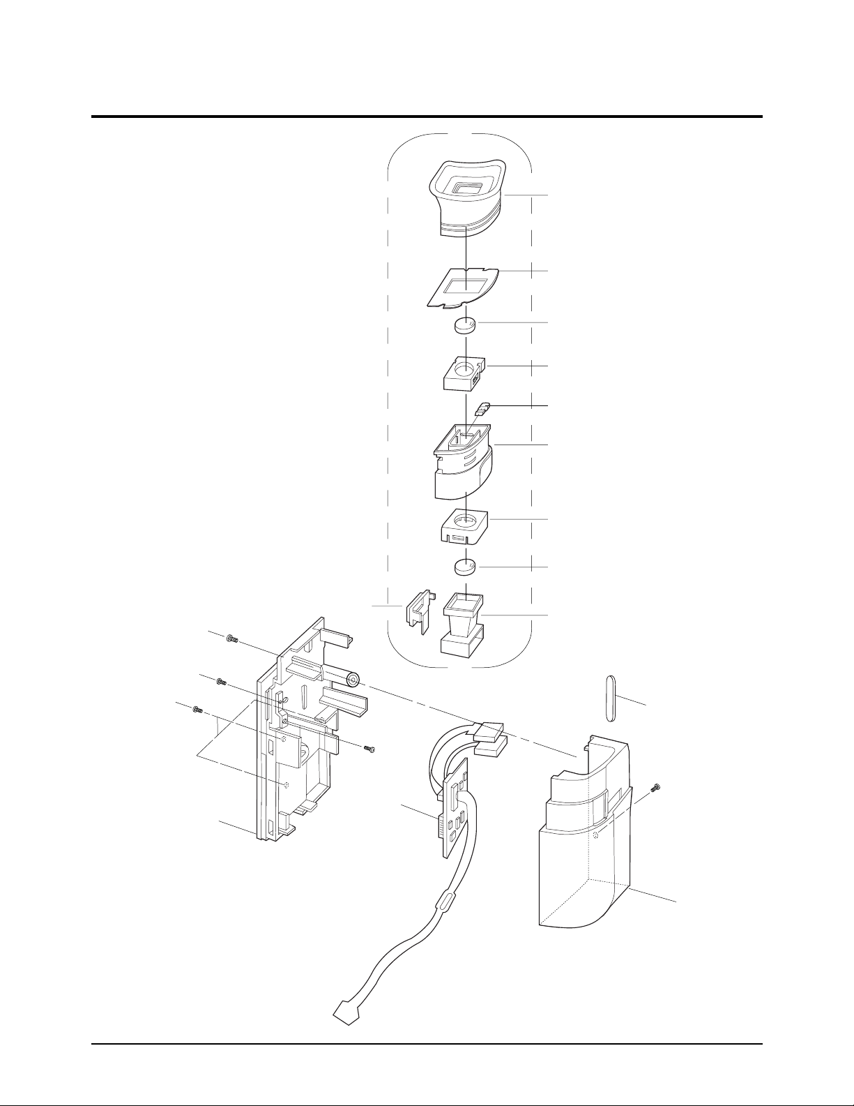
Samsung Electronics5-10
Exploded View and Parts List
5-5 EVF
303
304
305
306
316
307
308
309
310
315
319
301
311
905
904
911
904
915
302
Page 77

Samsung Electronics 5-11
Exploded View and Parts List
Loc. No New Part No Description and Specification Remark
301 AD64-00247A CASE-EVF-L;-,NTSC,-,-,-,BW,1,M2 SCL500/L520/L530/L550
AD64-00247B CASE-EVF-L;-,PAL/BW,-,-,-,-,1,M2-PJ VP-L500/L520/L530/L530B/L550
302 AD64-00249A CASE-EVF R;-,ABS94VO,-,-,-,BW/COL,1,M2 SCL500/L520/L530/L550
AD64-00249A CASE-EVF R;-,ABS94VO,-,-,-,BW/COL,1,M2 VP-L500/L520/L530/L530B/L550
303 AD73-00020A RUBBER--EVF CUP;SILICON,BW/COL,M2,1 RU ALL
304 AD61-00306A GUIDE-CAP;-,ABS94HB BLK,-,-,BW/COL,1,M ALL
305 AD67-00027A LENS--EVF-M-G1;-,-,PMMA,4.5,D13.8,-,0.44 ALL
306 AD61-00233A HOLDER--CVF LENS;-,ABS94HB BLK,-,COL,-,M ALL
307 AD61-00305A GUIDE-LENS;-,ABS94HB,-,-,BW/COL,1,M2 ALL
308 AD61-00252A HOLDER-COVER-LENS;-,ABS84HB,-,BLK,-,M1-P ALL
309 AD67-00026A LENS--EVF-M-G2;-,-,PC,1.24,D11.2,-,EVF ALL
310 AD61-00228A HOLDER--CVF BOTTOM;-,ABS94VO,-,BLK,-,M1- ALL
311 AD61-00227A HOLDER--CVF TOP;-,ABS94VO,-,BLK,-,M1-PJ ALL
315 AD69-00112A PAD-EVF;M2-PJ,SPONGE,-,-,-,-,-,- ALL
316 AD64-00248A KNOB--EVF;-,POM BLK,-,BW/COL,-,M2,1 ALL
904 AC60-10055A SCREW-TAPPING;BH,+,-,M2,X4,FZB ALL
905 AC60-10054A SCREW-TAPPING;BH,+,-,M2,X6,FZB ALL
911 6001-001263 SCREW-MACHINE;BH,+,M2,L2.2,NI PLT,SWRCH1 ALL
915 6001-000795 SCREW-MACHINE;BH,+,M2,L3,ZPC(WHT),SWRCH1 ALL
Page 78

Samsung Electronics5-12
Exploded View and Parts List
5-6 Mechanical Parts (1)
004
305
302
005
401
021
402
005
301
303
001
304
003
002
Page 79

Samsung Electronics 5-13
Exploded View and Parts List
Loc. No New Part No Description and Specification Remark
001 AC60-12083A SCREW-MACHINE;B,BH,-,M1.7,L5,FE,WHT,-,002 AD60-10500E SCREW-MACHINE;-,BWSH,+,UP,M2,L5,ZPCNYLOK
003 AD60-10500D SCREW-MACHINE;-,BWSH,+,UP,M2,L7,ZPCNYLOK
004 AC60-10017A SCREW-MACHINE;BH,+,M1.7,X3.5,FEFZY,SWCH1
005 AC60-12112A SCREW-BH;-,BH,+,M1.4,L2,021 AC60-30015A WASHER-SLIT;ID 1.1,OD 2.6,T 0.4,POLYSLID
301 AD96-10473P ASS’Y-HOUSING;DE-6B,302 AD96-10471Z ASS’Y-DRUM;DE6A-PH-SS,- VP-L500/L520/L530/L530B/L550
AD96-10471Y ASS’Y-DRUM;DE6A-NH-SS,- SCL500/L520/L530/L550
303 AD66-40153A ROLLER-IMP ASS’Y;-,YF-10,OD7,-,DE-6
304 AC61-72009A CONTACT-EARTH BRUSH;SECC/PBSP/CR/C,-,-,305 AC63-32091A COVER-DRUM;DURACON(M90-44),-,-,-,-,-,DE401 AC63-30009A COVER-REEL ASS’Y;ABS 95,HB,-,-,-,-,DE-6,402 AC66-12035A IDLER-ASS’Y;-,-,DE-6
Page 80

Samsung Electronics5-14
Exploded View and Parts List
5-7 Mechanical Parts (2)
005
501
020
504
503
004
512
509
506
506
507
505
511
510
508
502
Page 81

Samsung Electronics 5-15
Exploded View and Parts List
Loc. No New Part No Description and Specification Remark
004 AC60-10017A SCREW-MACHINE;BH,+,M1.7,X3.5,FEFZY,SWCH1
005 AC60-12112A SCREW-BH;-,BH,+,M1.4,L2,020 AC60-30017A WASHER-SLIT;ID 1,OD 2.6,T 0.4,POLYSLIDER
501 AD31-12010A MOTOR-CAPSTAN;DE-6B SHS,-,-
AD31-12001Q MOTOR-CAPSTAN;DMCCHL06A(DE-6),-,502 AC66-22123A GEAR-CAPSTAN(ASS’Y);-,-,-,-,-,DE-6
503 AC66-22124A GEAR-PULLEY(ASS’Y);-,-,-,-,-,DE-6
504 AC66-62001A BELT-TIMMING;POLYURETHAN,L137 T0.4,-,-,505 AC66-32197A LEVER-CAM;SUS430-CP,T0.6,-,-,DE-6,506 AC66-42005A ROLLER-CAM MAIN;SUS303,-,-,PI3.5X1.1
507 AC66-22092A GEAR-CAM MAIN;SUS304-CSP,M0.5,Z64,-,-,508 AC66-82055A SLIDER-MAIN(ASS’Y);-,-,-,-,DE-6
509 AC66-32198A LEVER-EJECT;DURANEX #3300,-,-,-,DE-6,510 AC34-22001C SWITCH-MODE ASS’Y;HMW0484-01WA,DE-6,-,-,511 AC66-22126A GEAR-LOADING;DURACON(99-44),M0.4,Z37 WO,
512 AC31-12001P MOTOR-LOADING ASS’Y;DE-6,-,-
Page 82

Samsung Electronics5-16
Exploded View and Parts List
5-8 Mechanical Parts (3)
407
405
412
411
409
413 414
410
408
415
417
416
406
Page 83

Samsung Electronics 5-17
Exploded View and Parts List
Loc. No New Part No Description and Specification Remark
405 AD61-60622A SPRING-REVIEW ARM;PS SUS304-WPB PI0.3
406 AC61-52014A POLE-BASE S(ASS’Y);ZDC2/SUS303,-,-,-,-,DE
407 AC61-52015A POLE-BASE T(ASS’Y);ZDC2/SUS303,-,-,-,-,DE
408 AC66-32221A BRAKE-SUB S(ASS’Y);-,-,-,-,DE-6,409 AC66-12042A REEL-T(ASS’Y);-,-,-,DE-6
410 AC66-12041A REEL-S(ASS’Y);-,-,-,DE-6
411 AC66-32217A ARM-PINCH ROLLER(ASS;-,-,-,-,DE-6
412 AC66-32213A ARM-REVIEW ASS’Y;-,-,-,-,DE-6
413 AC66-32223A BRAKE-MAIN(T);DURACON(M904-44),-,-,-,-,414 AC66-30120A BRAKE-SOFT T (ASS’Y);-,-,-,-,DE-6,415 AC66-30093A ARM-TENSION (ASS’Y);SUS304-CSP POM FELT,416 AC61-62022A SPRING-SOFT BRAKE(S);-,SUS304,-,-,-,-,417 AC61-62023A SPRING-TENSION;-,SUS304-WPB,-,-,-,-,-
Page 84

Samsung Electronics5-18
Exploded View and Parts List
MEMO
MEMO
 Loading...