SAMSUNG SW_204B Service Manual
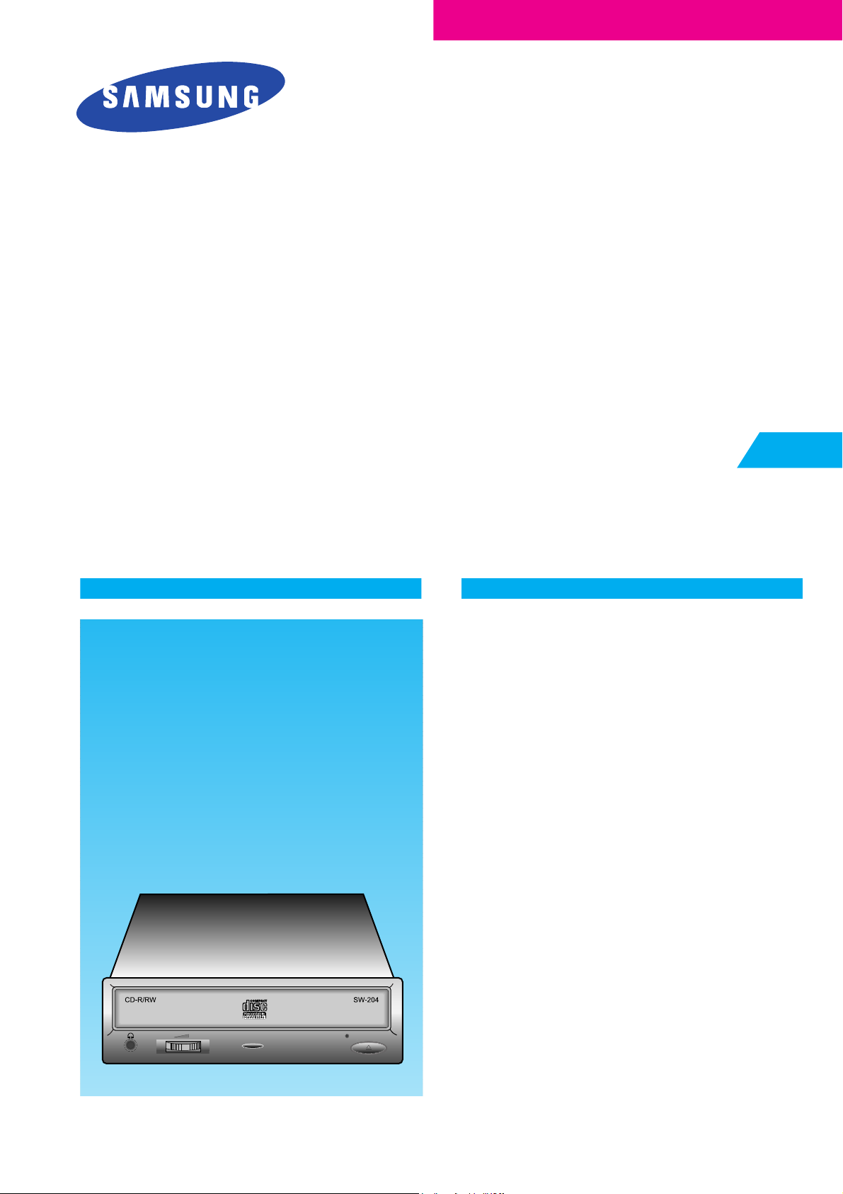
Model:SW-204B
CD-R/RW service manual
¥ Specifications
¥ Cautions at Service
¥ External Part Name
¥ Exploded Views & Part List
¥ Packing Options
¥ Block Diagram
¥ Troubleshooting
¥ Circuit Diagram
¥
Main Components Block Diagram & Pin
Descriptions
¥ Electrical Parts List
The design and part of this product is subject to change without prior notice for performance improvement.
CONTENTS

©
Samsung Electronics Co., Ltd.
AUGUST, 1999
Printed in Korea
Code No.: BG68-00060A
Electronics
2
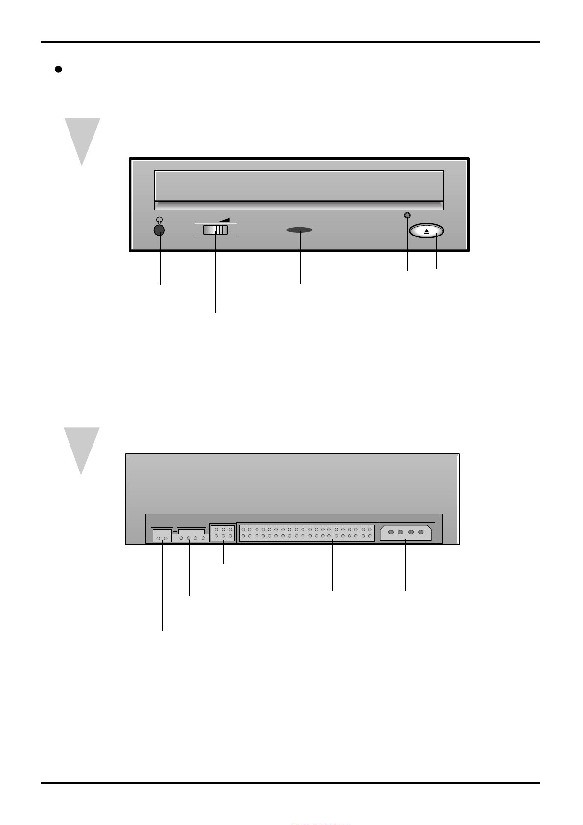
1. Front
2. Rear
Earphhone jack
Digital output terminal
(Optional)
Sound output terminal
Master/Slave select pin
Interface
terminal
Power terminal
Up/Down Volume
Stop/Open
button
LED
Emergency
HOLE
External Part Name

1
1. General Specifications
- Drive type : Computer built-in
- Power consumption : DC +5V, 1.5A
DC +12V, 1.5A
- Dimensions : 149mm(W)X42.5mm(H)X200mm(L)
- Net Weight : 950g
2. Electrical Features
- Interface : ATAPI BUS(IDE)
-
Data transfer rate :
Write(CD-R) : 150KBytes/Sec(1X)
300KBytes/Sec(2X)
600KBytes/Sec(4X)
Write(CD-RW) : 3,600KBytes/Sec(2X)
Resd(MAX) : 1,500~3.600KBytes/Sec(Cav10X~24X)
- Access time : 120ms (Random. TYPICAL)
- Buffer Capacity : 2Mbyte
- Error ratio : Mode 1: Below 10
-12
Mode 2: Below 10
-9
- Frequency response : 20Hz~20KHz (Lineout)
100Hz~20KHz (H/P out)
- Signal to noise ratio : 75dB(1KHz, Limeout)
- Distortion factor : 0.15% Less than(1KHz)
- Channel separation : 60dB(1KHz, Limeout)
55dB(1KHz, H/P out)
- Used laser : Semiconductor laser
- Audio Output : Line out 0.70 ±20%(vrms), 47K½
1. General Items
1) Be careful not to have your eyes or a part of body touch with-
laser diode at repair because this product uses laser diode.
2) Do not disassemble Pick-up at repair. If the laser diode is
bad, replace the entire Pick-up.
3) Keep away from TV or other electrical units at repair to
prevent influence from surrounding units.
4) If you replace the parts during repair, be sure to unplug the
power cable before replacement.
5) If you insert a disc into the drive, be sure to load it corectly.
6) Because this unit can't be used by itself, surely mount it
on PC (586 DMA support) and check the operations in
use of private device driver floppy diskette.
Refer to Instruction manual.
7) This unit has many parts with features related to safety and
especially, for essential parts, the importance is indicated on
circuit diagram and part list.
Be certain to use the parts with same specifications at
replaing these parts.
2.
Earthing cautions at handling Pick-up
- Because the laser diode in optical Pick-up is subject
to get out of order due to the potential difference occurring
by electricity load charged in clothes or bodies, observe the
following earthing items at handling.
1) Body earthing(hand) : Be sure to wear a wrist strip
with one side earthed.(Impedance : Below 104).
It removes the electricity formed in body.
2) Work table earthing : Put the earthed conductive plate
(Impedance : Below 104) such as copper plate on work
table.
3) Cautions for clothes : Do not have any clothes touch with
Pick-up because the electricity formed in clothes is
destroyed easily.
Specifications
Cautions at Service
26
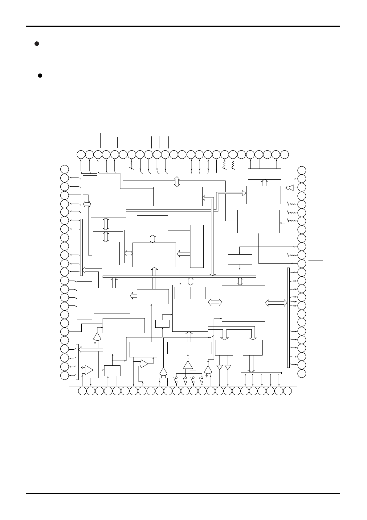
TC9450F(DSP CHIP)
+
Ð
+
Ð
+
Ð
+
Ð
+
Ð
75
74
73
72
71
70
69
68
67
66
65
64
63
62
61
60
59
58
57
56
55
54
53
52
51
1
2
AUDIO
OUT
VSS3
BCK
AOUT
DOUT
MBOV
IPF
SBOK
CLOCK
VDD3
VSS5
DATA
SFSY
SBSY
SPCK
SPDA
COFS
MONIT
VDD5
TESTIO0
AWRC
PVDD3
PDOS
PDO
TMAX
TMAXS
XVDD3
XO
XI
XVSS3
TEST2
TEST1
TEST0
TESIN
TESTIO1
FGIN
DACT
CKSE
DMOUT
IO3
IO2
IO1
IO0
VSS3
VDD3
FLGD
FLGC
FLGB
FLGA
SEL
VDD3
DIGITAL
OUT
SUBCODE
OUT
16K RAM
ROM RAM
DIGITAL
EQUALIZER
SERVO
CONTROL
DECODER
ERROR
CORECTION
MICOM
INTERFACE
CLOCK
GENERATOR
CAV
ADRESS
STATUS
LPF
DA COUNTER
3
4
5
6
7
8
9
10
11
12
13
14
15
16
17
18
19
20
21
22
23
24
25
9998979695949392919089888786858483828180797877
76
100
30292827263132333435363738394041424344454647484950
+
Ð
DA PWMCONVERTOR
DATA
SLICER
CLV
ACTIVE
WIDERANGE
PLL
TMAX
VCO
DVSS3
RO
DVDD3
DVR
LO
DVSS3
TEST3
TEST4
BUS0
BUS1
BUS2
BUS3
VDD5
VSS5
XRD
XWR
XCM
XCE
TEST5
RST
HSO
UHSO
SHSO
EMPH
LRCK
VSS3
DMO
FVO
FMO
TEBC
RFGC
VREF
TRO
FOO
TEZI
TEI
SBAD
FEI
RFRP
RFZI
RFCT
AVDD3
RFI
SLCO
AVSS3
VCOF
VCOREF
PVREF
LPFO
LPFN
Main Components Block Diagram and Pin Descrition
27
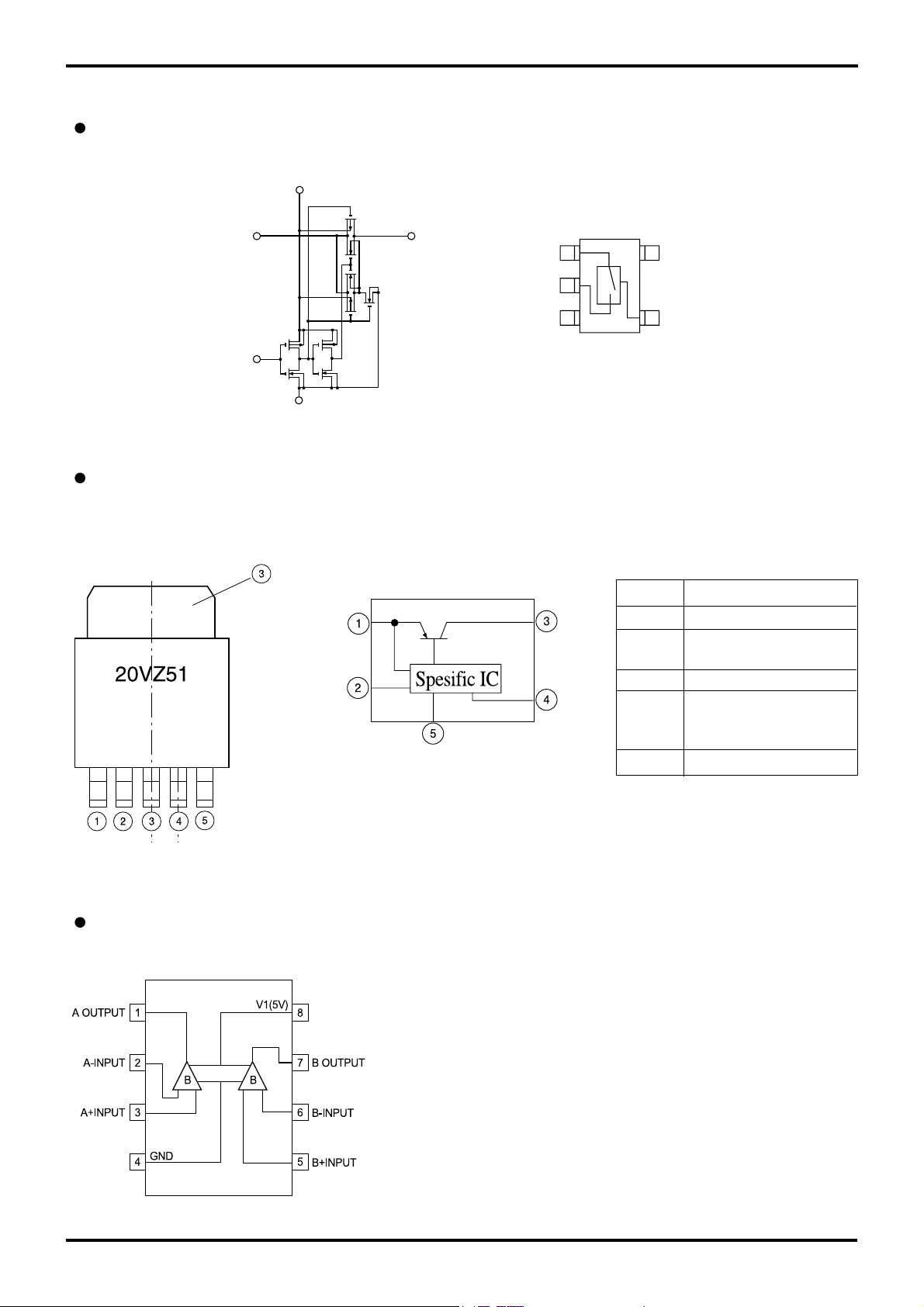
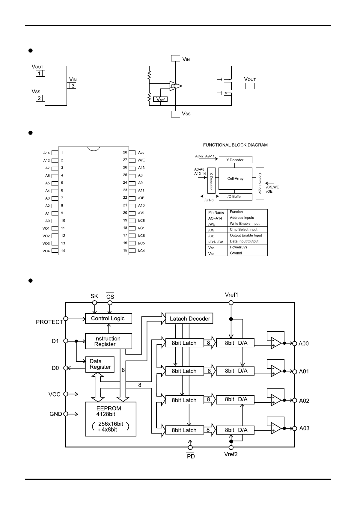
TC4S66F
NJM3414AV
PQ20WZ51
- Pin configlation
Pin No Pin Name
1
DC input(VIN)
2
ON/OFF control terminal(VC)
3 DC output(VO)
4
Output voltage minute
adjustment
terminal(VADJ)
5 GND
V
DD
CONTROL
IN/OUT
OUT/IN
V
SS
IN/OUT
OUT/IN
15
2
V
SS
3
4
V
DD
CONT
28
ELM9735
KM62256
AK9844
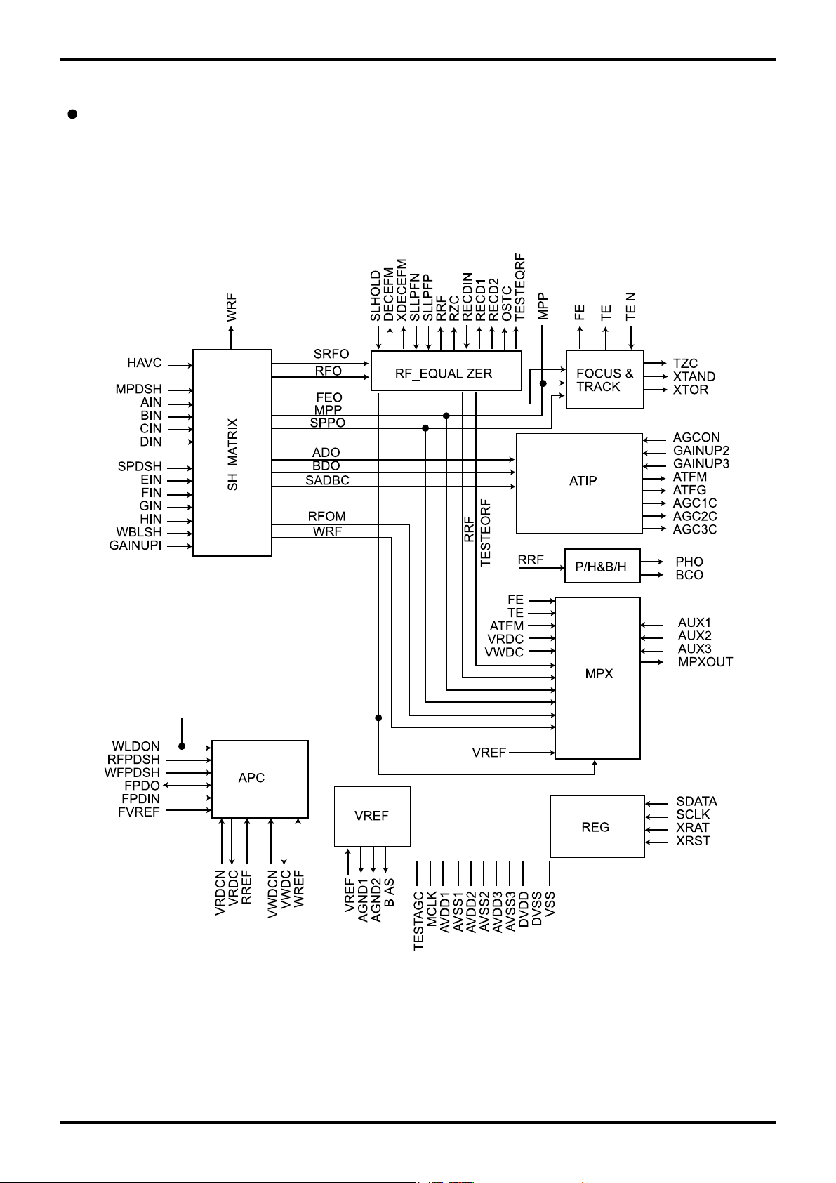
29
AK9844
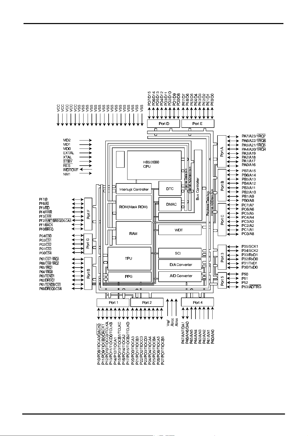
¡Ü
HBS/2350
30
 Loading...