

SAMSUNG S3C84I8X, S3F84I8X, S3C84I9X, S3F84I9X User Manual

USER’S MANUAL
S3C84I8X/F84I8X/
C84I9X/F84I9X
8-BIT CMOS MICROCONTROLLERS
June, 2007
REV 2.00
Confidential Proprietary of Samsung Electronics Co., Ltd
Copyright © 2007 Samsung Electronics, Inc. All Rights Reserved

Important Notice
The information in this publication has been carefully
checked and is believed to be entirely accurate at
the time of publication. Samsung assumes no
responsibility, however, for possible errors or
omissions, or for any consequences resulting from
the use of the information contained herein.
Samsung reserves the right to make changes in its
products or product specifications with the intent to
improve function or design at any time and without
notice and is not required to update this
documentation to reflect such changes.
This publication does not convey to a purchaser of
semiconductor devices described herein any license
under the patent rights of Samsung or others.
Samsung makes no warranty, representation, or
guarantee regarding the suitability of its products for
any particular purpose, nor does Samsung assume
any liability arising out of the application or use of
any product or circuit and specifically disclaims any
and all liability, including without limitation any
consequential or incidental damages.
S3C84I8X/F84I8X/C84I9X/F84I9X 8-Bit CMOS Microcontrollers
User's Manual, Revision 2.00
Publication Number: 22-S3-C84I8X/F84I8X/C84I9X/F84I9X-062007
"Typical" parameters can and do vary in different
applications. All operating parameters, including
"Typicals" must be validated for each customer
application by the customer's technical experts.
Samsung products are not designed, intended, or
authorized for use as components in systems
intended for surgical implant into the body, for other
applications intended to support or sustain life, or for
any other application in which the failure of the
Samsung product could create a situation where
personal injury or death may occur.
Should the Buyer purchase or use a Samsung
product for any such unintended or unauthorized
application, the Buyer shall indemnify and hold
Samsung and its officers, employees, subsidiaries,
affiliates, and distributors harmless against all
claims, costs, damages, expenses, and reasonable
attorney fees arising out of, either directly or
indirectly, any claim of personal injury or death that
may be associated with such unintended or
unauthorized use, even if such claim alleges that
Samsung was negligent regarding the design or
manufacture of said product.
Copyright © 2006-2007 Samsung Electronics Co., Ltd.
All rights reserved. No part of this publication may be reproduced, stored in a retrieval system, or transmitted in
any form or by any means, electric or mechanical, by photocopying, recording, or otherwise, without the prior
written consent of Samsung Electronics.
Samsung Electronics' microcontroller business has been awarded full ISO-14001
certification (BSI Certificate No. FM24653). All semiconductor products are designed
and manufactured in accordance with the highest quality standards and objectives.
Samsung Electronics Co., Ltd.
San #24 Nongseo-Dong, Giheung-Gu
Yongin-City, Gyeonggi-Do, Korea
C.P.O. Box #37, 446-711
TEL: (82)-(31)-209-5238
FAX: (82)-(31)-209-6494
Home Page: http://www.samsung.com
Printed in the Republic of Korea

NOTIFICATION OF REVISIONS
ORIGINATOR: Samsung Electronics, LSI Development Group, Gi-Heung, South Korea
PRODUCT NAME: S3C84I8X/F84I8X/C84I9X/F84I9X 8-bit CMOS Microcontroller
DOCUMENT NAME: S3C84I8X/F84I8X/C84I9X/F84I9X User's Manual, Revision 2.00
DOCUMENT NUMBER: 22- S3-C84I8X/F84I8X/C84I9X/F84I9X- 062007
EFFECTIVE DATE: June, 2007
SUMMARY: As a result of additional product testing and evaluation, some specifications
published in S3C84I8X/F84I8X/C84I9X/F84I9X User's Manual, Revision 1.00,
have been changed. These changes for in S3C84I8X/F84I8X/C84I9X/F84I9X
microcontroller, which are described in detail in the
Revision Descriptions section below, are related to the followings:
— Chapter 4. Control Registers
DIRECTIONS: Please note the changes in your copy (copies) of the
S3C84I8X/F84I8X/C84I9X/F84I9X User’s Manual,
Revision 1.00. Or, simply attach the Revision Descriptions of the next page to
S3C84I8X/F84I8X/C84I9X/F84I9X User’s Manual, Revision 1.00.
REVISION HISTORY
Revision Description of Change Refer to
1.00 First edition. T.H. Kim Nov, 2006
2.00 Second edition Page 4-17 T.H. Kim June, 2007
Author(s)
Date
REVISION DESCRIPTIONS
1. Chapter 4. Control Registers
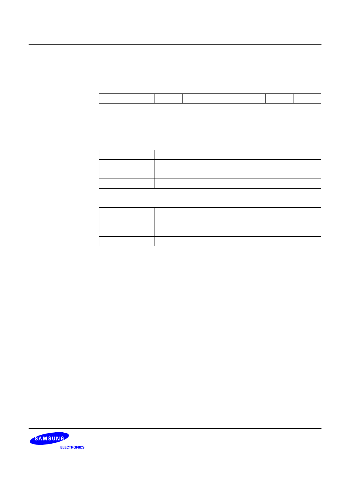
LPOT — LCD Port Control Register F7H Set 1, Bank1
Bit Identifier .7 .6 .5 .4 .3 .2 .1 .0
RESET Value
Read/Write
.7
.6–.4 SEG4-SEG19 and COM0-COM3 Selection Bit
.3 SEG3/P2.7 Selection Bit
.2 SEG2/P2.6 Selection Bit
.1 SEG1/P2.5 Selection Bit
.0 SEG0/P2.4 Selection Bit
– 0 0 0 0 0 0 0
– R/W R/W R/W R/W R/W R/W R/W
Not used for S3C84I8X/F84I8X/C84I9X/F84I9X
SEG4-7 SEG8-11 SEG12-15 SEG16-19/
COM7-COM4
P3.0-P3.3 P3.4-P3.7 P4.0-P4.3 P4.4-P4.7 P0.0-P0.3
0 0 0
0 1 0
1 0 0
1 0 1
1 1 0
1 1 1
0
Normal I/O port
1
SEG port
0
Normal I/O port
1
SEG port
0
Normal I/O port
1
SEG port
0
Normal I/O port
1
SEG port
Port Port Port Port Port
Port Port Port Port COM
SEG SEG SEG SEG/COM COM
Port SEG SEG SEG/COM COM
Port Port SEG SEG/COM COM
Port Port Port SEG/COM COM
COM0-3

USER'S MANUAL
ERRATA
This document contains the corrections of errors,
typos and omissions in the following document.
Samsung 8-bit CMOS S3C84I8X/F84I8X/C84I9X/F84I9X
Microprocessor User's Manual
Document Number: 02-2.00-S3-C84I8X/F84I8X/C84I9X/F84I9X-062007
Publication: June 2007
S3C84I8X/F84I8X/C84I9X/F84I9X_ERRATA_REV 2.00 USER’S MANUAL ERRATA
ERRATA (VER 2.00)
Samsung 8-bit CMOS S3C84I8X/F84I8X/C84I9X/F84I9X Microprocessor User’s Manual
Document Number: 02-2.00-S3- C84I8X/F84I8X/C84I9X/F84I9X-062007
Publication: June 2007
1. PIN ASSIGNMENT (PAGE 1-4)
INT0/TAOUT/P1.0
INT1/BUZ/TACK/P1.1
SDAT/INT2/TACAP/P1.2
SCLK/INT3/T1OUT1/P1.3
VDD
VSS
Xout
Xin
Vpp/TEST
Xtin
Xtout
P4.1/SEG13
P 4.7/SEG 19/C OM7
P 4.6/SEG 18/C OM6
P4.5/S EG17/C OM5
4443424140393837363534
1
2
3
4
5
6
7
8
9
10
11
S3C84I9X/F84I9X
S3C84I8X/F84I8X
(44-QFP)
1213141516171819202122
RESET
n
P4.2/S EG14
P4.3/S EG15
P4 .4/SEG1 6/C OM 4
Top View
P4.0/SEG12
P3.7/SEG11
P3.5/SEG9
P3.6/SEG10
33
32
31
30
29
28
27
26
25
24
23
P3.4/SEG8
P3.3/SEG7
P3.2/SEG6
P3.1/SEG5
P3.0/SEG4
P0.3/COM3/AD3
P0.2/COM 2/AD2
P0.1/COM 1/AD1
P0.0/COM0/AD0
Avss
Avref
SI/AD 7/P2. 3
Rx/SEG2 /P2.6
SO/S EG0/P2.4
T1CK1/AD5 /P 1.4
T1CAP1/AD6/P1.5
T1OUT0/AD4/P2.2
PWM/T1CAP0/P2.1
TBPWM/T1CK0/P2.0
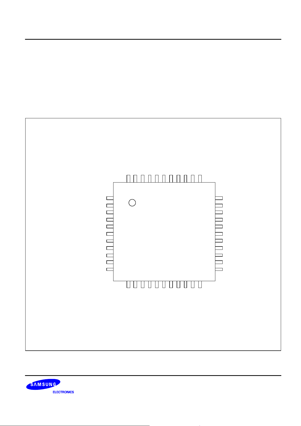
Figure 1-2. S3C84I8X/F84I8X/C84I9X/F84I9X Pin Assignment (44-pin QFP)
1
TX/S EG3/P2.7
SCK/ S EG1/P2 .5
USER’S MANUAL ERRATA S3C84I8X/F84I8X/C84I9X/F84I9X_ERRATA_REV 2.00
2. PIN ASSIGNMENT (PAGE 1-5)
SEG14/P4.2
SEG15P4.3
SEG16/COM4/P4.4
SEG17/COM5/P4.5
COM6/SEG18/P4.6
COM7/SEG19/P4.7
INT0/TAOUT/P1.0
INT1/BUZ/TACK/P1.1
SDAT/INT2/TACAP/P1.2
SCLK/INT3/T1OUT1/P1.3
VDD
VSS
Xout
Xin
Vpp/TEST
XTin
XTout
nRESET
TBPWM/T1CK0/P2.0
PWM/T1CAP0/P2.1
T1OUT0/AD4/P2.2
1
2
3
4
5
6
7
S3C84I9X/F84I9X
8
9
10
11
12
13
14
15
16
17
18
19
20
21
Top View
(42-SDIP)
42
41
40
39
38
37
36
35
34
33
32
31
30
29
28
27
26
25
24
23
22
P4.1/SEG13
P4.0/SEG12
P3.7/SEG11
P3.6/SEG10
P3.5/SEG9
P3.4/SEG8
P3.3/SEG7
P3.2/SEG6
P3.1/SEG5
P3.0/SEG4
AD3/COM3/P0.3
AD2/COM2/P0.2
AD1/COM1/P0.1
AD0/COM0/P0.0
AVss
AVref
P2.7/SEG3/TxD
P2.6/SEG2/RxD
P2.5/SEG1/SCK
P2.4/SEG0/SO
P2.3/AD7/SI
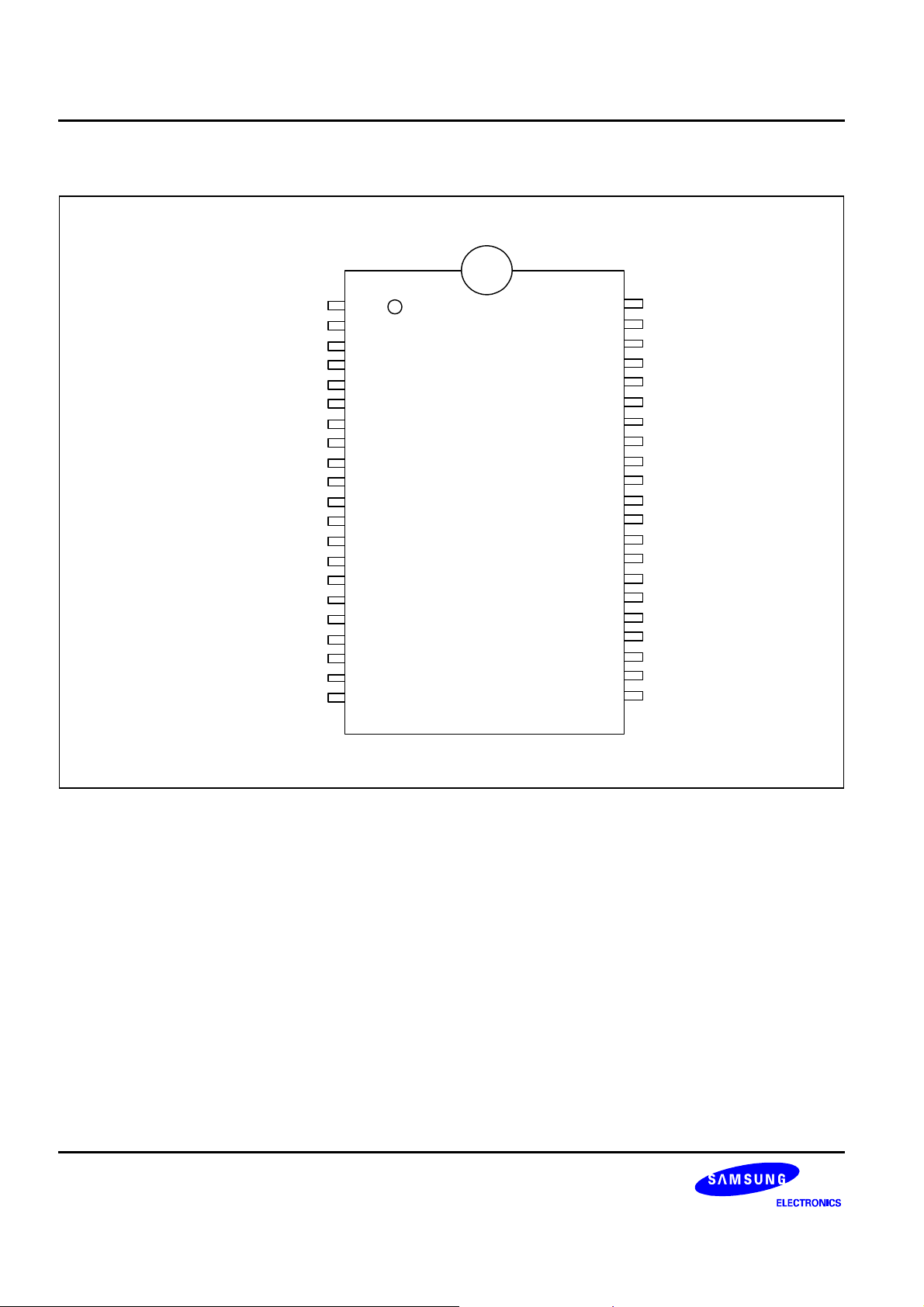
Figure 1-3. S3C84I9X/F84I9X Pin Assignment (42-pin SDIP)
2
S3C84I8X/F84I8X/C84I9X/F84I9X_ERRATA_REV 2.00 USER’S MANUAL ERRATA
3. PIN ASSIGNMENT (PAGE 1-14)
V
DD
V
DD
Data
Open Drain EN
Data
LCD Out EN
SEG
Type H-4
Output Disable
Normal Input
P-CH
N-CH
Circuit
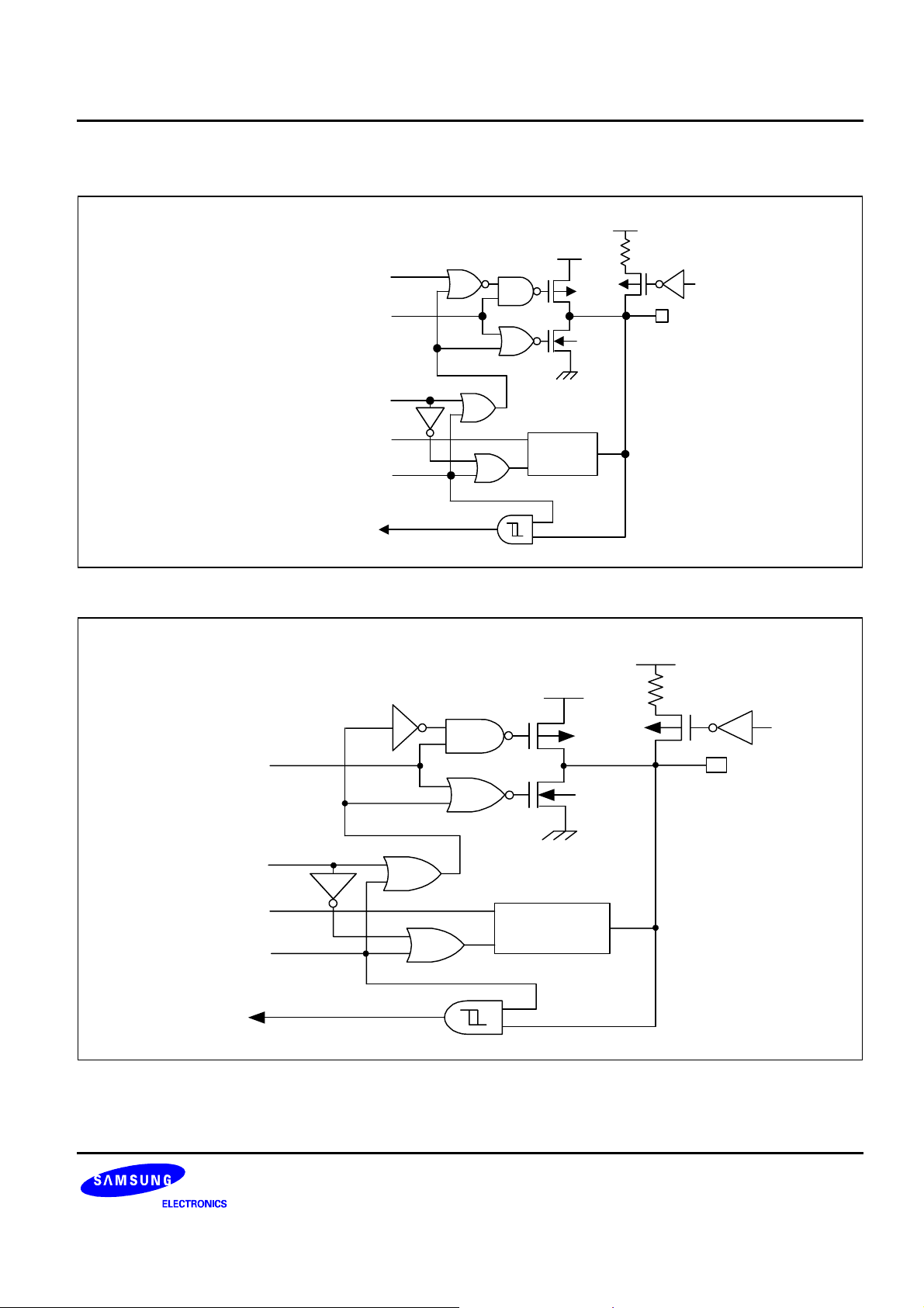
Figure 1-12. Pin Circuit Type H-17 (P3.0–P3.7, P4.0–P4.)
VDD
VDD
P-CH
Pull-up
Enable
I/O
Pull-up
Enable
I/O
LCD Out EN
Output Disable
Normal Input
N-CH
SEG
Circuit
Type H-4
Figure 1-13. Pin Circuit Type H-18 (2.4–P2.7)
3

USER’S MANUAL ERRATA S3C84I8X/F84I8X/C84I9X/F84I9X_ERRATA_REV 2.00
4. REGISTER ARCHITECTURE (PAGE 2-5)
64
Bytes
32
Bytes
FFH
E0H
DFH
D0H
CFH
C0H
13H
Set1
Bank 1
Bank 0
System and
Peripheral Control Registers
(Register Addressing Mode)
System and
Peripheral Control Registers
(Register Addressing Mode)
General Purpose Register
(Register Addressing Mode)
Page 2
FFH
E0H
192
Bytes
FFH
C0H
BFH
Page 1
Page 0
Set 2
General-Purpose
Data Registers
(Indirect Register, Indexed
Mode, and Stack Operations)
256
Bytes
Prime
Data Registers
(All Addressing Modes)
LCD Display Registers
00H
00H
NOTE: Page2's 00H~13H is used for LCD Display Registers(Write-only).
Figure 2-3. Internal Register File Organization of S3F84I9X/C84I9X
4
S3C84I8X/F84I8X/C84I9X/F84I9X_ERRATA_REV 2.00 USER’S MANUAL ERRATA
64
Bytes
32
Bytes
FFH
E0H
DFH
D0H
CFH
C0H
13H
00H
Set1
Bank 1
Bank 0
System and
Peripheral Control Registers
(Register Addressing Mode)
System and
Peripheral Control Registers
(Register Addressing Mode)
General Purpose Register
(Register Addressing Mode)
Page 2
LCD Display Registers
FFH
E0H
192
Bytes
FFH
C0H
BFH
00H
Page 0
Set 2
General-Purpose
Data Registers
(Indirect Register, Indexed
Mode, and Stack Operations)
256
Bytes
Page 0
Prime
Data Registers
(All Addressing Modes)
NOTE: Page2's 00H~13H is used for LCD Display Registers(Write only)
Figure 2-4. Internal Register File Organization of S3F84I8X/C84I8X
5

USER’S MANUAL ERRATA S3C84I8X/F84I8X/C84I9X/F84I9X_ERRATA_REV 2.00
5. REGISTER PAGE POINTER (PAGE 2-7)
Register Page Pointer (PP)
DFH ,Set 1, R/W
LSBMSB .7 .6 .5 .4 .3 .2 .1 .0
Destination register page selection bits:
0000 0000
0001
0002
NOTE:
Destination: Page 0
Destination: Page 1 Source: Page 1
Destination: Page 2
In the S3C84I9X/F84I9X microcontroller, page 0,1,2 are implemented.
In the S3C84I8X/F84I8X microcontroller, page 0,2 are implemented.
A hardware reset operation writes the 4-bit destination and source values shown
above to the register page pointer(00H). These values should be modified to
other pages
Source register page selection bits:
Source: Page 0
0001
0002
Source: Page 2
Figure 2-5. Register Page Pointer (PP)
6
S3C84I8X/F84I8X/C84I9X/F84I9X_ERRATA_REV 2.00 USER’S MANUAL ERRATA
6. CONTROL REGISTERS (PAGE 4-19)
P0CON — Port 0 Control Register (High Byte) E6H Set 1, Bank0
.7–.6 P0.3/AD3/COM3 Configration Bits
.5–.4 P0.2/AD2/COM2 Configration Bits
.3–.2 P0.1/ AD1/COM1 Configration Bits
.1–.0 P0.0/ AD0/COM0 Configration Bits
0 0 Input mode
0 1 Input mode with pull-up
1 0 Push-pull output mode
1 1 Alternative function mode; AD3 input
0 0 Input mode
0 1 Input mode with pull-up
1 0 Push-pull output mode
1 1 Alternative function mode; AD2 input
0 0 Input mode
0 1 Input mode with pull-up
1 0 Push-pull output mode
1 1 Alternative function mode; AD1 input
0 0 Input mode
0 1 Input mode with pull-up
1 0 Push-pull output mode
1 1 Alternative function mode; AD0 input
NOTE: If you want to use P0 as a LCD port, you must set LPOT register appropriately.(Refer to Ex .2 below)
If you want to use P0 as a Normal I/O or Alternative function(ADC0~ADC3), you must set LPOT register
appropriately. (Refer to Ex. 1 below)
For example,
(1) LD LPOT,#00000000B ; P0.0~P0.3 is Normal I/O or Alternative function(ADC0~ADC3).
(2) LD LPOT,#01001111B ; P0.0~P0.3 is LCD port.
For more detail, please refer to page 9-5
7

USER’S MANUAL ERRATA S3C84I8X/F84I8X/C84I9X/F84I9X_ERRATA_REV 2.00
7. CONTROL REGISTERS (PAGE 4-24)
P2CONH — Port 2 Control Register (High Byte) ECH Set 1, Bank0
.7–.6 P2.7/SEG3/TxD Configration Bits
.5-.4 P2.6/SEG2/RxD Configration Bits
.3–.2 P2.5/ SEG1/SCK Configration Bits
.1–.0 P2.4/SEG0/SO Configration Bits
0 0 Input mode
0 1 Alternative function mode: Not used
1 0 Push-pull output mode
1 1 Alternative function mode: TxD output
0 0 Input mode ; RxD input
0 1 Alternative function mode: Not used
1 0 Push-pull output mode
1 1 Alternative function mode: RxD output
0 0 Input mode ; SCK input
0 1 Alternative function mode: Not used
1 0 Push-pull output mode
1 1 Alternative function mode: SCK output
0 0 Input mode
0 1 Alternative function mode: Not used
1 0 Push-pull output mode
1 1 Alternative function mode: SO output
NOTE: If you want to use a P2 as LCD port, you must set LPOT register appropriately. (Refer to Ex. 2 below)
If you want to use a P2 as Normal I/O or Alternative function(SO/SCK/RxD/TxD), you must set LPOT
register appropriately. (Refer to Ex. 1 below)
For example,
(1) LD LPOT,#00000000B ; P2.4~P2.7 is Normal I/O or Alternative function(SO/SCK/RxD/TxD).
(2) LD LPOT,#01001111B ; P2.4~P2.7 is LCD port.
For more detail, please refer to page 9-13
8

S3C84I8X/F84I8X/C84I9X/F84I9X_ERRATA_REV 2.00 USER’S MANUAL ERRATA
8. CONTROL REGISTERS (PAGE 4-27)
P3CONH — Port 3 Control Register (High Byte) EEH Set 1, Bank0
.7–.6 P3.7/SEG11 Configration Bits
.5–.4 P3.6/SEG10 Configration Bits
.3–.2 P3.5/ SEG9 Configration Bits
.1–.0 P3.4/ SEG8 Configration Bits
0 0 Input mode
0 1 Input mode with pull-up
1 0 Push-pull output mode
1 1 N-channel open-drain output
0 0 Input mode
0 1 Input mode with pull-up
1 0 Push-pull output mode
1 1 N-channel open-drain output
0 0 Input mode
0 1 Input mode with pull-up
1 0 Push-pull output mode
1 1 N-channel open-drain output
0 0 Input mode
0 1 Input mode with pull-up
1 0 Push-pull output mode
1 1 N-channel open-drain output
NOTE: If you want to use P3 as a LCD port, you must set LPOT register appropriately. (Refer to Ex. 2 below)
If you want to use P3 as a Normal I/O, you must set LPOT register appropriately. (Refer to Ex. 1 below)
For example,
(1) LD LPOT,#00000000B ; P3.4~P3.7 is Normal I/O.
(2) LD LPOT,#01001111B ; P3.4~P3.7 is LCD port.
For more detail, please refer to page 9-16
9
USER’S MANUAL ERRATA S3C84I8X/F84I8X/C84I9X/F84I9X_ERRATA_REV 2.00
9. CONTROL REGISTERS (PAGE 4-28)
P3CONL — Port 3 Control Register (Low Byte) EFH Set 1, Bank0
.7–.6 P3.3/ SEG7 Configration Bits
.5–.4 P3.2/ SEG6 Configration Bits
.3–.3 P3.1/ SEG5 Configration Bits
.1–.0 P3.0/ SEG4 Configration Bits
0 0 Input mode
0 1 Input mode with pull-up
1 0 Push-pull output mode
1 1 N-channel open-drain output
0 0 Input mode
0 1 Input mode with pull-up
1 0 Push-pull output mode
1 1 N-channel open-drain output
0 0 Input mode
0 1 Input mode with pull-up
1 0 Push-pull output mode
1 1 N-channel open-drain output
0 0 Input mode
0 1 Input mode with pull-up
1 0 Push-pull output mode
1 1 N-channel open-drain output
NOTE: If you want to use P3 as a LCD port, you must set LPOT register appropriately. (Refer to Ex. 2 below)
If you want to use P3 as a Normal I/O, you must set LPOT register appropriately. (Refer to Ex. 1 below)
For example,
(1) LD LPOT,#00000000B ; P3.0~P3.3 is Normal I/O.
(2) LD LPOT,#01001111B ; P3.0~P3.3 is LCD port.
For more detail, please refer to page 9-16
10

S3C84I8X/F84I8X/C84I9X/F84I9X_ERRATA_REV 2.00 USER’S MANUAL ERRATA
10. CONTROL REGISTERS (PAGE 4-29)
P4CONH — Port 4 Control Register (High Byte) F0H Set 1, Bank0
.5–.4 P4.6/ COM6/SEG18 Configration Bits
.3–.3 P4.5/ COM5/SEG17 Configration Bits
.1–.0 P4.4/ COM4/SEG16 Configration Bits
0 0 Input mode
0 1 Input mode with pull-up
1 0 Push-pull output mode
1 1 N-channel open-drain output
0 0 Input mode
0 1 Input mode with pull-up
1 0 Push-pull output mode
1 1 N-channel open-drain output
0 0 Input mode
0 1 Input mode with pull-up
1 0 Push-pull output mode
1 1 N-channel open-drain output
0 0 Input mode
0 1 Input mode with pull-up
1 0 Push-pull output mode
1 1 N-channel open-drain output
NOTE: If you want to use P4 as a LCD port, you must set LPOT register appropriately. (Refer to Ex. 2 below)
If you want to use P4 as a Normal I/O, you must set LPOT register appropriately. (Refer to Ex. 1 below)
For example,
(1) LD LPOT,#00000000B ; P4.4~P4.7 is Normal I/O.
(2) LD LPOT,#01001111B ; P4.4~P4.7 is LCD port.
For more detail, please refer to page 9-19
11
USER’S MANUAL ERRATA S3C84I8X/F84I8X/C84I9X/F84I9X_ERRATA_REV 2.00
11. CONTROL REGISTERS (PAGE 4-30)
P4CONL — Port 4 Control Register (Low Byte) F1H Set 1, Bank0
.7–.6 P4.3/ BUZ/SEG15 Configration Bits
.5–.4 P4.2/ SEG14 Configration Bits
.3–.2 P4.1/ SEG13 Configration Bits
.1–.0 P4.0/ SEG12 Configration Bits
0 0 Input mode
0 1 Input mode with pull-up
1 0 Push-pull output mode
1 1 N-channel open-drain output
0 0 Input mode
0 1 Input mode with pull-up
1 0 Push-pull output mode
1 1 N-channel open-drain output
0 0 Input mode
0 1 Input mode with pull-up
1 0 Push-pull output mode
1 1 N-channel open-drain output
0 0 Input mode
0 1 Input mode with pull-up
1 0 Push-pull output mode
1 1 N-channel open-drain output
NOTE: If you want to use P4 as a LCD port, you must set LPOT register appropriately. (Refer to Ex. 2 below)
If you want to use P4 as a Normal I/O, you must set LPOT register appropriately. (Refer to Ex. 1 below)
For example,
(1) LD LPOT,#00000000B ; P4.0~P4.3 is Normal I/O.
(2) LD LPOT,#01001111B ; P4.0~P4.3 is LCD port.
For more detail, please refer to page 9-19
12
S3C84I8X/F84I8X/C84I9X/F84I9X_ERRATA_REV 2.00 USER’S MANUAL ERRATA
12. CONTROL REGISTERS (PAGE 4-31)
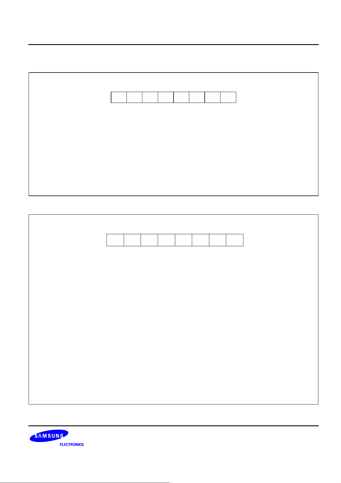
PP — Register Page Pointer DFH Set 1
Bit Identifier .7 .6 .5 .4 .3 .2 .1 .0
RESET Value
Read/Write
Addressing Mode
.7–.4 Destination Register Page Selection Bits
0 0 0 0 Destination: page 0
0 0 0 1 Destination: page 1
0 0 1 0 Destination: page 2
Other values Don’t care
.3–.0 Source Register Page Selection Bits
0 0 0 0 Source: page 0
0 0 0 1 Source: page 1
0 0 1 0 Source: page 2
Other values Don’t care
0 0 0 0 0 0 0 0
R/W R/W R/W R/W R/W R/W R/W R/W
Register addressing mode only
NOTES:
1. In the S3C84I8X/F84I8X microcontroller, the internal register file is configured as two pages (Page 0, Page 2).
The page 0 is used for the general-purpose register file and data register.
2. In the S3C84I9X/F84I9X microcontroller, the internal register file is configured as three pages (Page 0-2)
The page 0 and page 1 are used for the general-purpose register file and data register .
3. The page 2 is used for the LCD display ram and it is a write-only memory.
13

USER’S MANUAL ERRATA S3C84I8X/F84I8X/C84I9X/F84I9X_ERRATA_REV 2.00
13. PORT CONTROL REGISTERS (PAGE 9-5)
) PROGRAMMING TIP — To make P0 as Normal I/O or Alternative function
ORG 0100H ; Reset address
START DI
•
•
SB1
LD LPOT,# 00H ; P0 is normal I/O or alternative function
SB0
LD P0CON,#00H ; P0 is input mode
LD P0CON,#055H ; P0 is input pull-up mode
•
LD P0CON,#0AAH ; P0 is Push-pull output mode
LD P0CON,#0FFH ; P0 is ADC input
• SB1
LD LPOT,# 4FH ; P0 is LCD port
SB0
LD P0CON,#0AAH ; If you use P0 as LCD port,P0CON register value doesn’t care
14
S3C84I8X/F84I8X/C84I9X/F84I9X_ERRATA_REV 2.00 USER’S MANUAL ERRATA
14. PORT CONTROL REGISTERS (PAGE 9-7)
Port 1 Control Register, High Byte (P1CONH)
E8H, Set1, Bank0, R/W, Reset value="00"
.7 .6 .5 .4 .3 .2 .1 .0MSB LSB
[.7-.4] Not used(must keep always 0)
[.3-.2] P1.5/T1CAP1/AD6 Configuration Bits
0 0 = Input mode; T1CAP1 input
0 1 = Input mode with pull-up; T1CAP1 input
1 0 = Push-pull output mode
1 1 = Alternative function mode: AD6
[.1-.0] P1.4/T1CK1/AD5 Configuration Bits
0 0 = Input mode; T1CK1 input
0 1 = Input mode with pull-up; T1CK1 input
1 0 = Push-pull output mode
1 1 = Alternative function mode: AD5
Figure 9-2. Port 1 High-Byte Control Register (P1CONH)
Port 1 Control Register, Low By te (P 1 CONL)
E9H, Set1, Bank0, R/W, Reset value="00H"
.7 .6 .5 .4 .3 .2 .1 .0MSB LSB
[.7-.6] P1.3/T1OUT1/INT3 Configuration Bits
0 0 = Input mode; Interrupt input (INT3)
0 1 = Input mode with pull-up; Interrupt input (INT3)
1 0 = Push-pull output mode
1 1 = Alternative function mode: T1OUT1 output
[.5-.4] P1.2/TACAP/INT2 Configuration Bits
0 0 = Input mode; Interrupt input (INT2); TACAP
0 1 = Input mode with pull-up; Interrupt input (INT2);TACAP
1 0 = Push-pull output mode
1 1 = Alternative function mode: Not used
[.3-.2] P1.1/TACK/BUZ/INT1 Configuration Bits
0 0 = Input mode; Interrupt input (INT1); TACK
0 1 = Input mode with pull-up ; Interrupt input (INT1); TACK
1 0 = Push-pull output mode
1 1 = Alternative function mode: BUZ output
[.1-.0] P1.0/TAOUT/INT0 Configuration Bits
0 0 = Input mode; Interrupt input (INT0)
0 1 = Input mode with pull-up; Interrupt input (INT0)
1 0 = Push-pull output mode
1 1 = Alternative function mode: TAOUT output
Figure 9-3. Port 1 Low-Byte Control Register (P1CONL)
15
USER’S MANUAL ERRATA S3C84I8X/F84I8X/C84I9X/F84I9X_ERRATA_REV 2.00
15. PORT CONTROL REGISTERS (PAGE 9-9)
PORT 2
Port 2 is an 8-bit I/O port with individually configurable pins. Port 2 pins are accessed directly by writing or reading
the port 2 data register, P2 at location E2H in set 1, bank 0. P2.0–P2.7 can serve as digital inputs, outputs (push
pull) or you can configure the following alternative functions:
— General-purpose digital I/O
— Alternative function: SEG0-SEG3, ADC4, ADC7, SI, T1CAP0, T1OUT0, T1CK0, TBPWM, PWM
.
16. PORT CONTROL REGISTERS (PAGE 9-10)
Port 2 Control Register, High Byte (P2CONH)
ECH, Set1, Bank0, R/W, Reset value="00"
.7 .6 .5 .4 .3 .2 .1 .0MSB LSB
[.7-.6] P2.7/SEG3/TxD Configuration Bits
0 0 = Input mode
0 1 = Alternative function mode; Not used
1 0 = Push-pull output mode
1 1 = Alternative function mode; TxD output
[.5-.4] P2.6/SEG2/RxD Configuration Bits
0 0 = Input mode; RxD iput
0 1 = Alternative function mode; Not used
1 0 = Push-pull output mode
1 1 = Alternative function mode; RxD output
[.3-.2] P2.5/SEG1/SCK Configuration Bits
0 0 = Input mode; SCK input
0 1 = Alternative function mode; Not used
1 0 =
Push-pull output mode
1 1 = Alternative function mode; SCK output
[.1-.0] P2.4/SEG0/SO Configuration Bits
0 0 = Input mode
0 1 = Alternative function mode; Not used
1 0 = Push-pull output mode
1 1 = Alternative function mode; SO output
Figure 9-6. Port 2 High-Byte Control Register (P2CONH)
16

S3C84I8X/F84I8X/C84I9X/F84I9X_ERRATA_REV 2.00 USER’S MANUAL ERRATA
17. PORT CONTROL REGISTERS (PAGE 9-11)
Port 2 Control Register, Low Byte (P2CONL)
EDH, Set1, Bank0, R/W, Reset value="00"
.7 .6 .5 .4 .3 .2 .1 .0MSB LSB
[.7-.6] P2.3/AD7/SI Configuration Bits
0 0 = Input mode; SI
0 1 = Alternative function mode; Not used
1 0 = Push-pull output mode
1 1 = Alternative function mode; AD7
[.7-.6] P2.2/AD4/T1OUT0 Configuration Bits
0 0 = Input mode
0 1 = Alternative function mode; T1OUT0
1 0 = Push-pull output mode
1 1 = Alternative function mode; AD4
[.7-.6] P2.1/PWM/T1CAP0 Configuration Bits
0 0 = Input mode; T1CAP0
0 1 = Alternative function mode; Not used
1 0 = Push-pull output mode
1 1 = Alternative function mode; PWM
[.7-.6] P2.0/TBPWM/T1CK0 Configuration Bits
0 0 = Input mode;T1CK0
0 1 = Alternative function mode; T1CK0
1 0 = Push-pull output mode
1 1 = Alternative function mode; TBPWM
Figure 9-7. Port 2 Low-Byte Control Register (P2CONL)
17

USER’S MANUAL ERRATA S3C84I8X/F84I8X/C84I9X/F84I9X_ERRATA_REV 2.00
18. PORT CONTROL REGISTERS (PAGE 9-13)
) PROGRAMMING TIP — To make P2 as Normal I/O or Alternative function
ORG 0100H ; Reset address
START DI
•
•
SB1
LD LPOT,# 00H ; P2 is normal I/O or alternative function
SB0
LD P2CONH,#00H ; P2 is input mode
LD P2CONH,#0AAH ; P2 is Push-pull output mode
•
LD P2CONH,#0FFH ; P2 is TXOUT,RXOUT,SCK OUT,SO OUT
• SB1
LD LPOT,# 04FH ; P2 is LCD port
SB0
LD P2CONH,#0AAH ; If you use P2 as LCD port,P2CONH register value doesn’t care
LD P2PUR,#00H ; P2PUR is disabled when P2 is used as a LCD port.
18

S3C84I8X/F84I8X/C84I9X/F84I9X_ERRATA_REV 2.00 USER’S MANUAL ERRATA
19. PORT CONTROL REGISTERS (PAGE 9-15)
Port 3 Control Register, Low Byte (P3CONL)
EFH, Set1, Bank0, R/W, Reset value="00"
.7 .6 .5 .4 .3 .2 .1 .0MSB LSB
[.7-.6] P3.3/SEG7 Configuration Bits
0 0 = Input mode
0 1 = Input mode with pull-up
1 0 = Push-pull output mode
1 1 = N-channel open-drain output
[.5-.4] P3.2/SEG6 Configuration Bits
0 0 = Input mode
0 1 = Input mode with pull-up
1 0 = Push-pull output mode
1 1 = N-channel open-drain output
[.3-.2] P3.1/SEG5 Configuration Bits
0 0 = Input mode
0 1 = Input mode with pull-up
1 0 = Push-pull output mode
1 1 = N-channel open-drain output
[.1-.0] P3.0/SEG4 Configuration Bits
0 0 = Input mode
0 1 = Input mode with pull-up
1 0 = Push-pull output mode
1 1 = N-channel open-drain output
Figure 9-10. Port 3 Low-Byte Control Register (P3CONL)
19

USER’S MANUAL ERRATA S3C84I8X/F84I8X/C84I9X/F84I9X_ERRATA_REV 2.00
20. PORT CONTROL REGISTERS (PAGE 9-16)
) PROGRAMMING TIP — To make P3 as Normal I/O or Alternative function
ORG 0100H ; Reset address
START DI
•
•
SB1
LD LPOT,# 00H ; P3 is normal I/O or alternative function
SB0
LD P3CONH,#00H ; P3 is input mode
LD P3CONL,#00H ; P3 is input mode
•
LD P3CONH,#55H ; P3 is input mode with pull-up
LD P3CONL,#55H ; P3 is input mode with pull-up
LD P3CONH,#0AAH ; P3 is Push-pull output mode
LD P3CONL,#0AAH ; P3 is Push-pull output mode
LD P3CONH,#0FFH ; P3 is N-channel open-drain output
LD P3CONL,#0FFH ; P3 is N-channel open-drain output
• SB1
LD LPOT,# 04FH ; P3 is LCD port
SB0
LD P3CONH,#0AAH ; If you use P3 as LCD port,P3CONH register value doesn’t care
LD P3CONL,#0AAH ; If you use P3 as LCD port,P3CONL register value doesn’t care
20

S3C84I8X/F84I8X/C84I9X/F84I9X_ERRATA_REV 2.00 USER’S MANUAL ERRATA
21. PORT CONTROL REGISTERS (PAGE 9-19)
) PROGRAMMING TIP — To make P4 as Normal I/O or Alternative function
ORG 0100H ; Reset address
START DI
•
•
SB1
LD LPOT,#00H ; P4 is normal I/O or alternative function
SB0
LD P4CONH,#00H ; P4 is input mode
LD P4CONL,#00H ; P4 is input mode
•
LD P4CONH,#55H ; P4 is input mode with pull-up
LD P4CONL,#55H ; P4 is input mode with pull-up
LD P4CONH,#0AAH ; P4 is Push-pull output mode
LD P4CONL,#0AAH ; P4 is Push-pull output mode
LD P4CONH,#0FFH ; P4 is N-channel open-drain output
LD P4CONL,#0FFH ; P4 is N-channel open-drain output
• SB1
LD LPOT,# 4FH ; P4 is LCD port
SB0
LD P4CONH,#0AAH ; If you use P4 as LCD port,P3CONH register value doesn’t care
LD P4CONL,#0AAH ; If you use P4 as LCD port,P3CONL register value doesn’t care
21

USER’S MANUAL ERRATA S3C84I8X/F84I8X/C84I9X/F84I9X_ERRATA_REV 2.00
22. FUNCTION DESCRIPTION (PAGE 11-2)
Capture Mode
In capture mode, a signal edge that is detected at the TACAP pin opens a gate and loads the current counter
value into the Timer A data register. You can select rising or falling edges to trigger this operation.
Timer A also gives you capture-input source: the signal edge at the TACAP pin. You select the capture input by
setting the value of the Timer A capture input selection bit in the port 1 control register, P1CONL, (set 1, bank 0,
E9H). When P1CONL.5-.4 is ‘00’ or ‘01’, the TACAP input or normal input is selected. When P1CONL.5-.4 is set
to 1X, normal push-pull output is selected.
Both kinds of timer A interrupts can be used in capture mode: the timer A overflow interrupt is generated
whenever a counter overflow occurs; the timer A match/capture interrupt is generated whenever the counter
value is loaded into the Timer A data register.
22

S3C84I8X/F84I8X/C84I9X/F84I9X_ERRATA_REV 2.00 USER’S MANUAL ERRATA
23. FUNCTION DESCRIPTION (PAGE 13-1)
PWM
The 10-bit PWM circuits have the following components:
— 8-bit comparator and extension cycle circuit
— 8-bit reference data register (PWMDATAH .7–.0)
— 2-bit extension data register (PWMDATAL .1–.0)
— PWM output pins (P2.1/PWM)
24. PWM CONTROL REGISTER (PAGE 13-5)
PWM Control Register (PWMCON)
F5H, R/W, Re set: 00H
.7 .6 .5 .4 .3 .2 .1 .0 LSBMSB
PWM input clock
selection bits:
OSC
OSC
OSC
OSC
/64
/8
/2
/1
PWM counter clear bit:
0 = No effect
1 = Clear the PWM counter
00 = f
01 = f
10 = f
11 = f
Not used for
S3C84I8X/F84I8X/C84I9X/F84I9X
PWMDATA reload
interval selection bit:
0 = reload from 10bit
up counter overflow
1 = reload from 8bit
up counter overflow
PWM counter enable bit:
0 = Stop counter
1 = Start (resume countering)
PWM OVF interrupt pending bit:
0 = No interrupt pending
0 = Clear pending condition (when write)
1 = Interrupt pending
PWM OVF interrupt enable bit:
0 = Disable interrupt
1 = Enable interrupt
Figure 13-3. PWM Control Register (PWMCON)
23
USER’S MANUAL ERRATA S3C84I8X/F84I8X/C84I9X/F84I9X_ERRATA_REV 2.00
25. UART BAUD RATE DATA REGISTER (PAGE 15-7)
Table 15-1. Commonly Used Baud Rates Generated by 16bit BRDATA
Baud Rate Oscillation Clock
76,800 Hz 10 MHz 0 0H 7 7H
38,400 Hz 10 MHz 0 0H 15 FH
19,200 Hz 10 MHz 0 0H 31 1FH
9,600 Hz 10 MHz 0 0H 64 40H
4,800 Hz 10 MHz 0 0H 129 81H
2,400 Hz 10 MHz 1 1H 3 3H
600 Hz 10 MHz 4 4H 16 10H
38,461 Hz 8 MHz 0 0H 12 0CH
12,500 Hz 8 MHz 0 0H 39 27H
19,230 Hz 4 MHz 0 0H 12 0CH
9,615 Hz 4 MHz 0 0H 25 19H
BRDATAH BRDATAL
Decimal Hex Decimal Hex
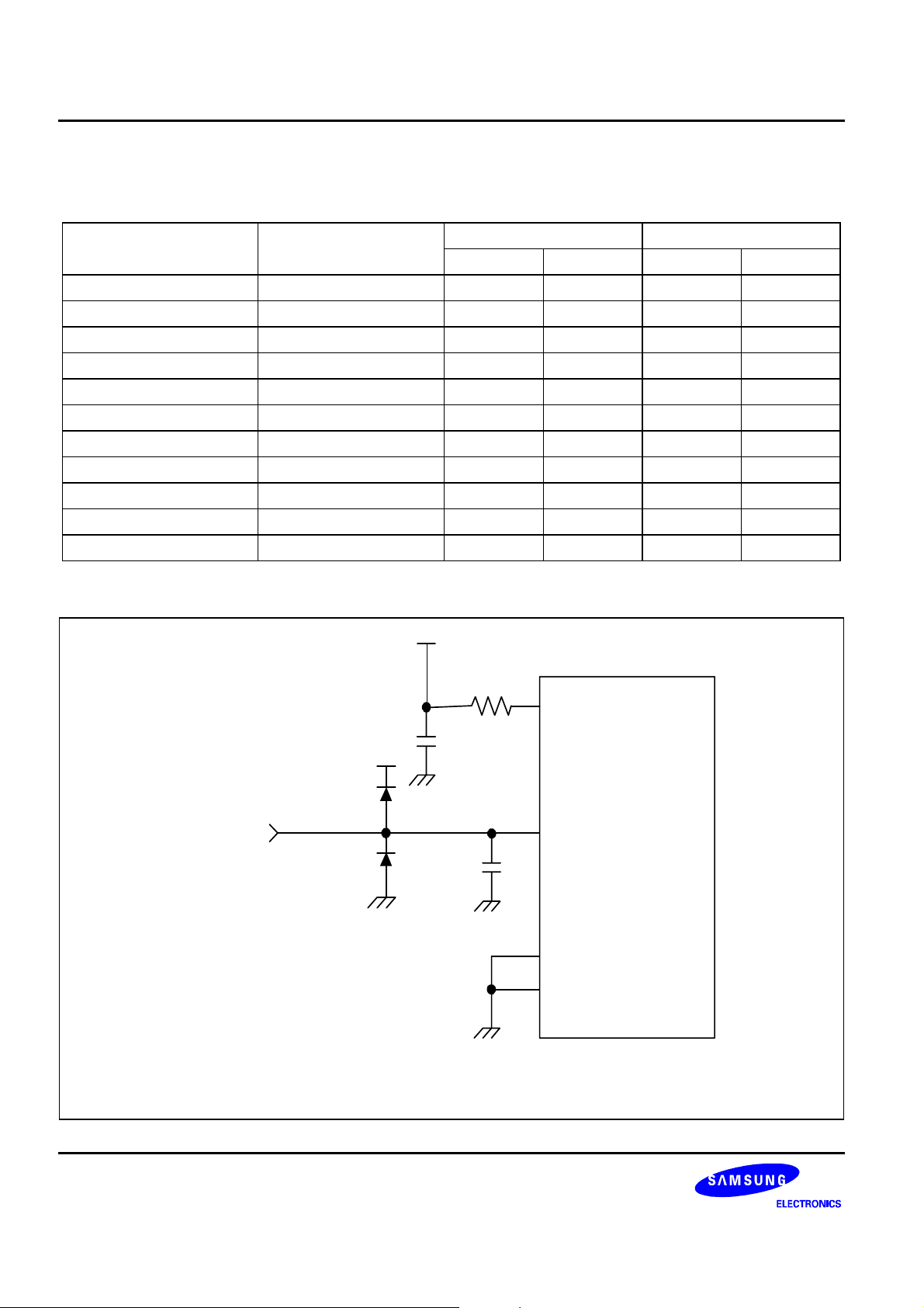
26. Internal A/D Conversion Procedure (PAGE 16-5)
V
DD
R
AVref
104
V
DD
Analog
Input Pin
101
ADC0-
ADC7
S3C84I9X/F84I9X
S3C84I8X/F84I8X
AVss
Vss
NOTES:
1. The symbol "R" signifies an offset res istor with a value of from50 to 100Ω
2. Avref must be tied to Vdd.
Figure 16-5. Recommended A/D Converter Circuit for Highest Absolute Accuracy
24
S3C84I8X/F84I8X/C84I9X/F84I9X_ERRATA_REV 2.00 USER’S MANUAL ERRATA
27. LCD RAM ADDRESS AREA (PAGE 18-3)
RAM addresses of page 2 are used as LCD data memory. It is Write-only memory.
When the bit value of a display segment is "1", the LCD display is turned on; when the bit value is "0", the display
is turned off.
Display RAM data are sent out through segment pins SEG0–SEG19 using a direct memory access (DMA)
method that is synchronized with the f
LCD
signal.
28. TOOL PROGRAM MODE (PAGE 20-1, 20-2)
Table 20-1. Descriptions of Pins Used to Read/Write the Flash ROM
Main Chip During Programming
Pin Name Pin Name Pin No. I/O Function
P1.2 SDAT 3 (44-pin)
9 (42-pin)
P1.3 SCLK 4 (44-pin)
10 (42-pin)
TEST VPP 9 (44-pin)
15 (42-pin)
nRESET nRESET 12 (44-pin)
18 (42-pin)
VDD/VSS VDD/VSS
5/6 (44-pin)
11/12 (42-pin)
I/O Serial data pin (output when reading, Input
when writing) Input and push-pull output port
can be assigned
I Serial clock pin (input only pin)
I Power supply pin for flash ROM cell writing
(indicates that MTP enters into the writing
mode). When 12.5 V (S3F84I8) /
Vdd(S3F84I9) is applied, MTP is in writing
mode.
I
I Logic power supply pin.
Table 21-2. Comparison of S3F84I8X/F84I9X and S3C84I8X/C84I9X Features
Characteristic S3F84I8X/84I9X S3C84I8X/84I9X
Program Memory 8 Kbyte Flash ROM for S3F84I8X
32 Kbyte Flash ROM for S3F84I9X
Operating Voltage (VDD)
2.5 V to 5.5 V (LVR off)
LVR to 5.5 V (LVR on)
= 5 V, VPP = 12.5 V (S3F84I8X)
MTP Programming Mode
V
DD
8 Kbyte Mask ROM for S3C84I8X
32 Kbyte Mask ROM for S3C84I9X
2.5 V to 5.5 V (LVR off)
LVR to 5.5 V (LVR on)
5V (S3F84I9X)
Pin Configuration 44QFP / 42SDIP
EPROM Programmability User Program multi time Programmed at the factory
25
 Loading...