

Page 1

现货库存、技术资料、百科信息、热点资讯,精彩尽在鼎好!
S3C4530A PRODUCT OVERVIEW
1 PRODUCT OVERVIEW
INTRODUCTION
Samsung's S3C4530A 16/32-bit RISC microcontroller is a cost-effective, high-performance microcontroller
solution for Ethernet-based systems. An integrated Ethernet controller, the S3C4530A, is designed for use in
managed communication hubs and routers.
The S3C4530A is built around an outstanding CPU core: the 16/32-bit ARM7TDMI RISC processor designed by
Advanced RISC Machines, Ltd. The ARM7TDMI core is a low-power, general purpose microprocessor macro-cell
that was developed for use in application-specific and custom-specific integrated circuits. Its simple, elegant, and
fully static design is particularly suitable for cost-sensitive and power-sensitive applications.
The S3C4530A offers a configurable 8-Kbyte unified cache/SRAM and Ethernet controller which reduces total
system cost. Most of the on-chip function blocks have been designed using an HDL synthesizer and the
S3C4530A has been fully verified in Samsung's state-of-the-art ASIC test environment.
Important peripheral functions include two HDLC channels with buffer descriptor, two UART channels with full
modem interface signal and 32byte buffer, 2-channel GDMA, two 32-bit timers, and 26 programmable I/O ports.
On-board logic includes an interrupt controller, DRAM/ SDRAM controller, and a controller for ROM/SRAM and
flash memory. The System Manager includes an internal 32-bit system bus arbiter and an external memory
controller.
The following integrated on-chip functions are described in detail in this user's manual:
— 8-Kbyte unified cache/SRAM
— I2C interface
— Ethernet controller
— HDLC controller
— GDMA
— UART
— Timers
— Programmable I/O ports
— Interrupt controller
1-1
Page 2

PRODUCT OVERVIEW S3C4530A
FEATURES
Architecture
• Integrated system for embedded ethernet
applications
• Fully 16/32-bit RISC architecture
• Little/Big-Endian mode supported basically, the
internal architecture is big-endian.
So, the little-endian mode only support for
external memory.
• Efficient and powerful ARM7TDMI core
• Cost-effective JTAG-based debug solution
• Boundary scan
System Manager
• 8/16/32-bit external bus support for
ROM/SRAM, flash memory, DRAM, and
external I/O
• One external bus master with bus request/
acknowledge pins
• Support for EDO/normal or SDRAM
• Programmable access cycle (0-7 wait cycles)
• Four-word depth write buffer
• Cost-effective memory-to-peripheral DMA
interface
Unified Instruction/Data Cache
• Two-way, set-associative, unified 8-Kbyte cache
• Support for LRU (least recently used) protocol
• Cache is configurable as an internal SRAM
• Data alignment logic
• Endian translation
• 100/10-Mbit per second operation
• Full compliance with IEEE standard 802.3
• MII(10/100Mbps) or 7-wire 10-Mbps interface
• Station management signaling
• On-chip CAM (up to 21 destination addresses)
• Full-duplex mode with PAUSE feature
• Long/short packet modes
• PAD generation
HDLCs
• HDLC protocol features:
— Flag detection and synchronization
— Zero insertion and deletion
— Idle detection and transmission
— FCS generation and detection (16-bit)
— Abort detection and transmission
• Address search mode (expandable to 4 bytes)
• Selectable CRC or No CRC mode
• Automatic CRC generator preset
• Digital PLL block for clock recovery
• Baud rate generator
• NRZ/NRZI/FM/Manchester data formats for
Tx/Rx
• Loop-back and auto-echo modes
I2C Serial Interface
• Master mode operation only
• Baud rate generator for serial clock generation
Ethernet Controller
• DMA engine with burst mode
• DMA Tx/Rx buffers (256 bytes Tx, 256 bytes
Rx)
• MAC Tx/Rx FIFO buffers (80 bytes Tx, 16 bytes
Rx)
1-2
• Tx/Rx FIFOs have 8-word (8 × 32-bit) depth
• Selectable 1-word or 4-word data transfer mode
• Data alignment logic
• Endian translation
• Programmable interrupts
• Modem interface
• Up to 10 Mbps operation
• HDLC frame length based on octets
• 2-channel DMA buffer descriptor for Tx/Rx on
each HDLC
Page 3

S3C4530A PRODUCT OVERVIEW
DMA Controller
• 2-channel General DMA for memory-tomemory, memory-to-UART, UART-to-memory
data transfers without CPU intervention
• Initiated by a software or external DMA request
• Increments or decrements a source or
destination address in 8-bit, 16-bit or 32-bit data
transfers
• 4-data burst mode
UARTs
• Two UART (serial I/O) blocks with DMA-based
or interrupt-based operation
• High speed(460Kbps) UART support with 32
byte Tx/Rx FIFO and modem interface signals
• Support for 5-bit, 6-bit, 7-bit, or 8-bit serial data
transmit and receive
• Automatic baud rate detection
• Eight control character comparison for software
control
• Programmable baud rates
• 1 or 2 stop bits
• Odd or even parity
• Break generation and detection
Programmable I/O
• 26 programmable I/O ports
• Pins individually configurable to input, output, or
I/O mode for dedicated signals
Interrupt Controller
• 21 interrupt sources, including 4 external
interrupt sources
• Normal or fast interrupt mode (IRQ, FIQ)
• Prioritized interrupt handling
PLL
• The external clock can be multiplied by on-chip
PLL to provide high frequency system clock
• The input frequency range is 10-40 MHz
• The output frequency is 5 times of input clock.
To get 50 MHz, input clock frequency should be
10 MHz.
Operating Voltage Range
• 3.3 V ± 5 %
Operating Temperature Range
• 0 oC to + 70 oC
• Parity, overrun, and framing error detection
• ×16 clock mode
• Infra-red (IR) Tx/Rx support (IrDA)
Timers
• Two programmable 32-bit timers
• Interval mode or toggle mode operation
Operating Frequency
• Up to 50 MHz
Package Type
• 208 pin QFP
1-3
Page 4
PRODUCT OVERVIEW S3C4530A
SCL
SDA
26 I/O Ports including
4: Ext INT req.
2: Timer out (0,1)
2: Ext DMA REQ.
2: Ext DMA ACK
14: UART
Console or
Modem I/F
ARM7TDMI
32-bit RISE CPU
CPU Interface
8-Kbyte
Unified
Cache
4-Word
Write
Buffer
Bus Rounter
I2C
26 General I/O ports
Interruput Controller
UART 0,1
32-bit Timer 0,1
Memory
Controller
with
Refresh
Control
System
Bus
Arbiter
2-Channel HDLCs
with DMAs
Ethernet Controller
2-channel BDMA
BDMA RAMs
Tx Buffer (256 bytes)
Rx Buffer (256 bytes)
CAM (128 bytes)
6-bank
ROM
SRAM
FLASH
4-bank
DRAM
4-bank
External
I/O
Device
External
Bus
Master
Remote
port A,B
1-4
GDMA 0,1
PLL
Tx FIFO (80 bytes)
Rx FIFO (16 bytes)
TAP Controller for JTAG
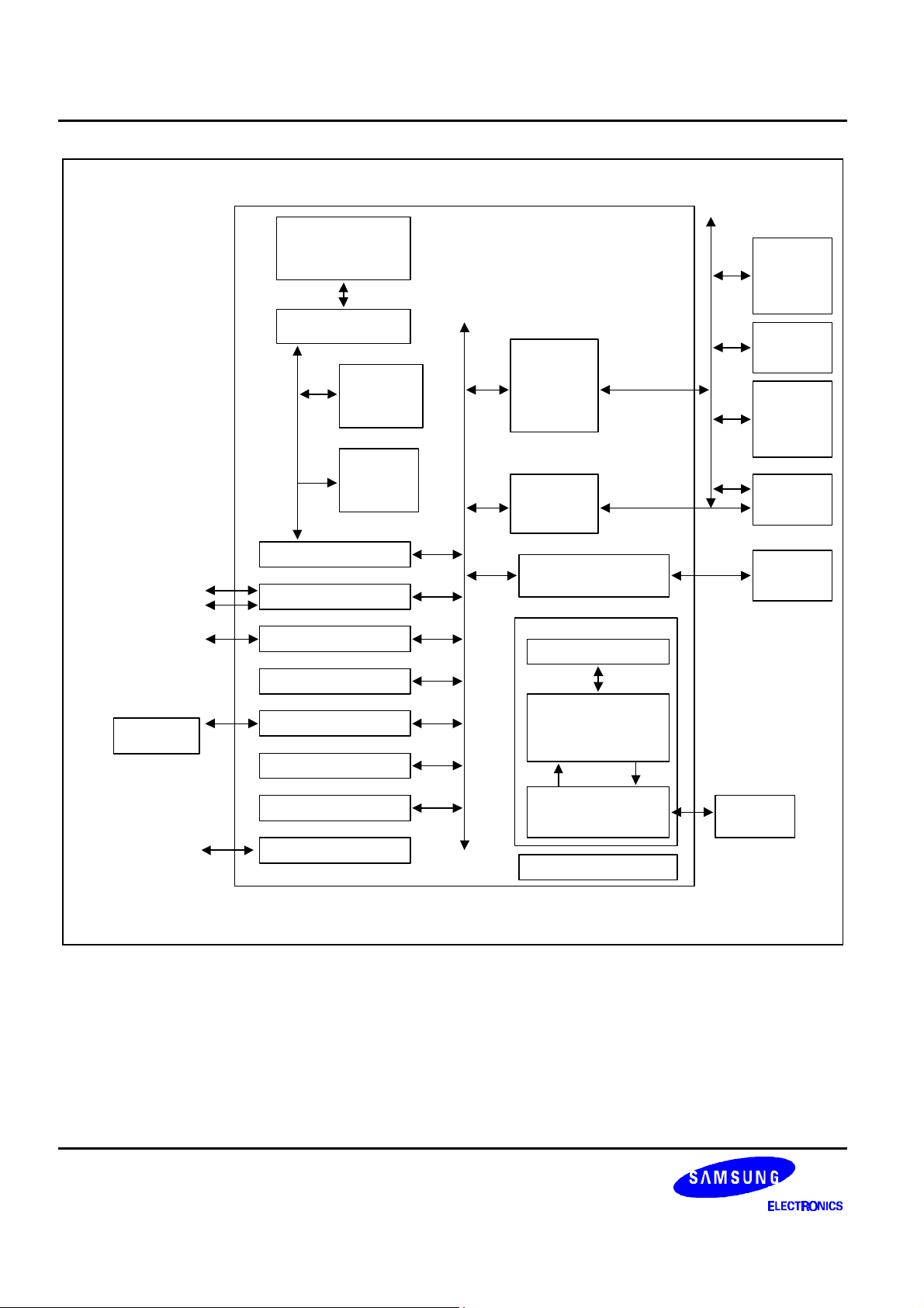
Figure 1-1. S3C4530A Block Diagram
MAC
MII or
7-wire
Page 5
S3C4530A PRODUCT OVERVIEW
VSS
VDDUARXD1/P<22>
nUADTR0/P<21>
UATXD0/P<20>
nUADSR0/P<19>
UARXD0/P<18>
SDA
SCA
P<17>/TOUT1
VSS
VDDP<16>/TOUT0
P<15>/nXDACK<1>
P<14>/nXDACK<0>
P<13>/nXDREQ<1>
P<12>/nXDREQ<0>
P<11>/XINREQ<3>
P<10>/XINREQ<2>
P<9>/XINREQ<1>
VSSVDDP<8>/XINREQ<0>
P<7>/nUARTS1
P<6>/nUACTS1
P<5>/nUADCD1
P<4>/nUARTS0
P<3>/nUACTS0
P<2>/nUADCD0
P<1>
VSSVDDP<0>
XDATA<31>
XDATA<30>
XDATA<29>
XDATA<28>
XDATA<27>
XDATA<26>
XDATA<25>
VSSVDD
XDATA<24>
XDATA<23>
XDATA<22>
XDATA<21>
XDATA<20>
XDATA<19>
XDATA<18>
XDATA<17>
VSSVDD
208
207
206
205
204
203
202
201
200
199
198
197
196
195
194
193
192
191
190
189
188
187
186
185
184
183
182
181
180
179
178
177
176
175
174
173
172
171
170
169
168
167
166
165
164
163
162
161
160
159
158
V
nUADSR1/P<23>
nUADTR1/P<25>
RX DV/LINK_10M
RXD<0>/RXD_10M
RX_CLK/RXCLK_10M
TXD<0>/TXD_10M
TXD<1>/LOOP_10M
Tx_ERR/POCMP_10M
TXCLK/TXCLK_10M
TX_EN/TXEN_10M
V
UATXD1/P<24>
nDTRA
RXDA
nRTSA
TXDA
nCTSA
V
V
nDCDA
RXCA
nSYNCA
TXCA
nDTRB
RxDB
nRTSB
TXDB
VDD
V
nCTSB
nDCDB
RXCB
nSYNCB
TXCB
CRS/CRS_ 10M
VDD
V
RXD<1>
RXD<2>
RXD<3>
RX ERR
COL/COL_10M
V
V
TXD<2>
TXD<3>
MDIO
LITTLE
MDC
V
VSS
157
100
101
102
103
156
155
154
153
152
151
150
149
148
147
146
145
144
143
142
141
140
139
138
137
136
135
134
133
132
131
130
129
128
127
126
125
124
123
122
121
120
119
118
117
116
115
114
113
112
111
110
109
108
107
106
105
104
DD
1
SS
2
3
4
5
6
7
8
9
10
DD
11
SS
12
13
14
15
16
17
18
19
20
21
SS
22
23
24
25
26
27
28
29
30
31
SS
32
33
34
35
36
37
38
39
40
DD
41
SS
42
43
44
45
46
47
48
49
50
DD
51
52
5354555657585960616263646566676869707172737475767778798081828384858687888990919293949596979899
S3C4530A
(208-QFP)
SS
V
VDD
XDATA<16>
XDATA<15>
XDATA<14>
XDATA<13>
XDATA<12>
XDATA<11>
XDATA<10>
XDATA<9>
XDATA<8>
XDATA<7>
XDATA<6>
VSS
DD
V
XDATA<5>
XDATA<4>
XDATA<3>
XDATA<2>
XDATA<1>
XDATA<0>
ADDR<21>
ADDR<20>
ADDR<19>
ADDR<18>
SS
V
DD
V
ADDR<17>
ADDR<16>
ADDR<15>
ADDR<14>
ADDR<13>
ADDR<12>
ADDR<11>
ADDR<10>/AP
ADDR<9>
ADDR<8>
SS
V
VDD
ADDR<7>
ADDR<6>
ADDR<5>
ADDR<4>
ADDR<3>
ADDR<2>
ADDR<1>
ADDR<0>
ExtMACK
ExtMREQ
nWBE<3>/DQM<3>
VSS
DD
V
SS
DD
DDa
VSSa
V
FILTER
TDI
V
V
TCK
TMS
TD0
nTRST
TMODE
UCLK
DD
V
SS
V
nECS<0>
nECS<1>
nECS<2>
nECS<3>
nOE
nEWAIT
CLKOEN
nRCS<0>
BOSIZE<0>
BOSIZE<1>
DD
VSS
VSS
V
XCLK
SDCLK/MCLKO
nRESET
CLKSEL
nRCS<1>
nRCS<2>
nRCS<3>
nRCS<4>
DD
VSS
V
nRCS<5>
nSDCS<0>/nRAS<0>
nSDCS<1>/nRAS<1>
nSDCS<2>/nRAS<2>
nDWE
nCAS<3>
CKE/nCAS<2>
nSDRAS/nCAS<0>
nSDCAS/nCAS<2>
nSDCS<3>/nRAS<3>
DQM<0>/nWBE<0>
SS
V
VDD
DQM<1>/nWBE<1>
DQM<2>/nWBE<2>
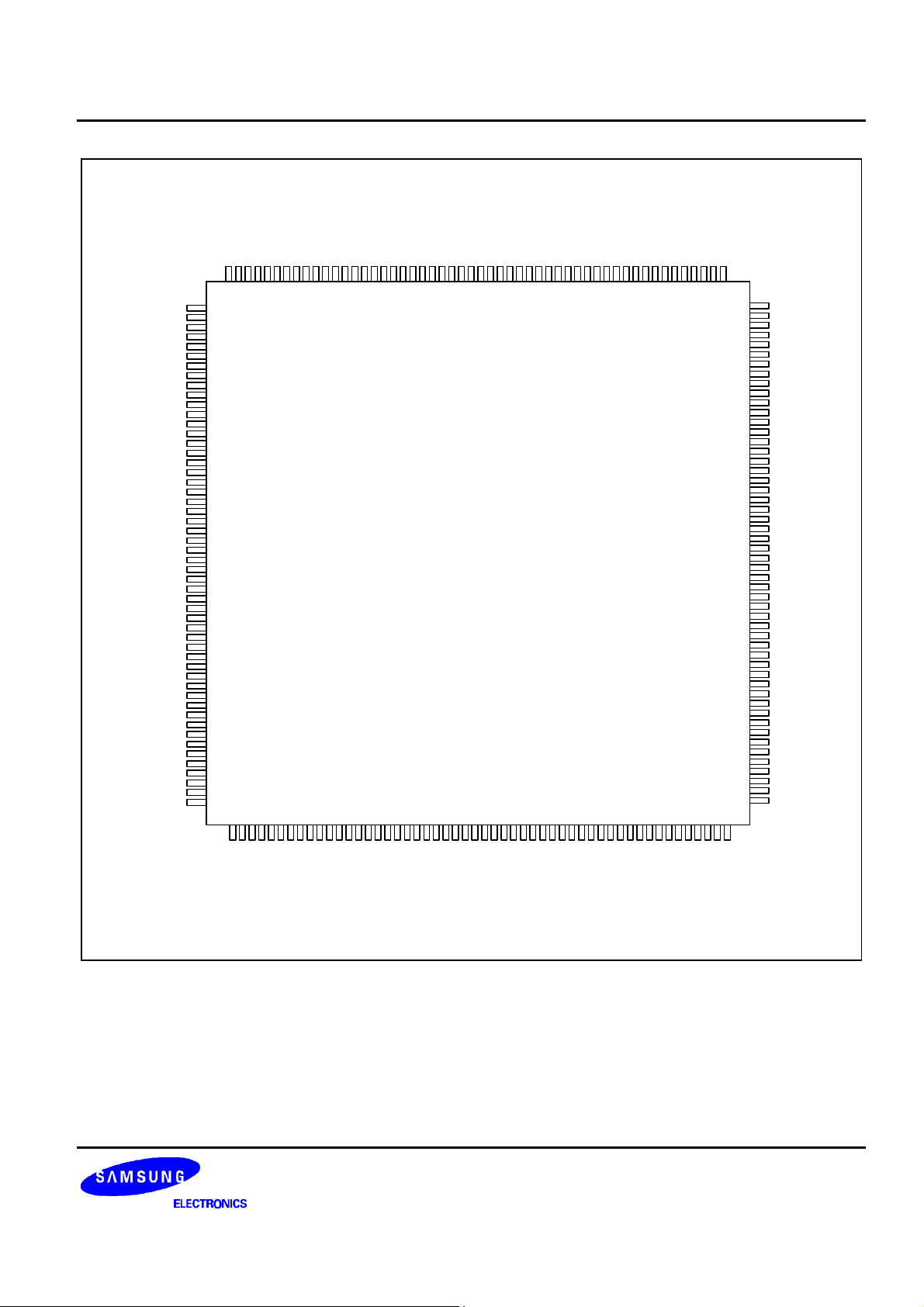
Figure 1-2. S3C4530A Pin Assignment Diagram
1-5
Page 6

PRODUCT OVERVIEW S3C4530A
SIGNAL DESCRIPTIONS
Table 1-1. S3C4530A Signal Descriptions
Signal Pin No. Type Description
XCLK 80 I S3C4530A System Clock source. If CLKSEL is Low, PLL output
clock is used as the S3C4530A internal system clock. If CLKSEL
is High, XCLK is used as the S3C4530A internal system clock.
MCLKO/SDCLK (1) 77 O System Clock Out. MCLKO is monitored as the inverting phase
of internal system clock, SCLK.
SDCLK is system clock for SDRAM
CLKSEL 83 I Clock Select. When CLKSEL is '0'(low level), PLL output clock
can be used as the master clock. When CLKSEL is '1'(high
level), the XCLK is used as the master clock.
nRESET 82 I Not Reset. nRESET is the global reset input for the S3C4530A.
To allow a system reset, and for internal digital filtering, nRESET
must be held to Low level for at least 64 master clock cycles.
Refer to "Figure 3. S3C4530A reset timing diagram" for more
details about reset timing.
CLKOEN 76 I Clock Out Enable/Disable. (See the pin description for MCLKO.)
TMODE 63 I Test Mode. The TMODE bit settings are interpreted as follows:
'0' = normal operating mode, '1' = chip test mode.
This TMODE pin also can be used to change MF of PLL.
To get 5 times internal system clock from external clock, '0'(low
level) should be assigned to TMODE. If '1'(high level), MF will be
changed to 6.6.
FILTER 55 AI If the PLL is used, 820pF capacitor should be connected between
the pin and analog ground.
TCK 58 I JTAG Test Clock. The JTAG test clock shifts state information
and test data into, and out of, the S3C4530A during JTAG test
operations. This pin is internally connected pull-down.
TMS 59 I JTAG Test Mode Select. This pin controls JTAG test operations
in the S3C4530A. This pin is internally connected pull-up.
TDI 60 I JTAG Test Data In. The TDI level is used to serially shift test
data and instructions into the S3C4530A during JTAG test
operations. This pin is internally connected pull-up.
TDO 61 O JTAG Test Data Out. The TDO level is used to serially shift test
data and instructions out of the S3C4530A during JTAG test
operations.
nTRST 62 I JTAG Not Reset. Asynchronous reset of the JTAG logic.
This pin is internally connected pull-up.
1-6
Page 7

S3C4530A PRODUCT OVERVIEW
Table 1-1. S3C4530A Signal Descriptions (Continued)
Signal Pin No. Type Description
ADDR[21:0]/
ADDR[10]/AP (1)
117-110,
129-120,
135-132
O Address Bus. The 22-bit address bus, ADDR[21:0], covers the full
4M word address range of each ROM/SRAM, flash memory,
DRAM, and the external I/O banks.
The 23-bit internal address bus used to generate DRAM address.
The number of column address bits in DRAM bank can be
programmed 8bits to 11bits use by DRAMCON registers.
ADDR[10]/AP is the auto pre-charge control pin. The auto precharge command is issued at the same time as burst read or
burst write by asserting high on ADDR[10]/AP.
XDATA[31:0] 141-136,
154-144,
I/O External (bi-directional, 32-bit) Data Bus. The S3C4530A data
bus supports external 8-bit, 16-bit, and 32-bit bus sizes.
166-159,
175-169
nRAS[3:0]/
nSDCS[3:0] (1)
94, 91, 90,
89
O Not Row Address Strobe for DRAM. The S3C4530A supports up
to four DRAM banks. One nRAS output is provided for each
bank. nSDCS[3:0] are chip select pins for SDRAM.
nCAS[3:0]
nCAS[0]/nSDRAS
nCAS[1]/nSDCAS
nCAS[2]/CKE (1)
98, 97, 96,
95
O Not column address strobe for DRAM. The four nCAS outputs
indicate the byte selections whenever a DRAM bank is accessed.
nSDRAS is row address strobe signal for SDRAM. Latches row
addresses on the positive going edge of the SDCLK with
nSDRAS low. Enable row access and pre-charge. nSDCAS is
column address strobe for SDRAM. Latches column addresses
on the positive going edge of the SDCLK with nSDCAS low.
Enables column access. CKE is clock enable signal for SDRAM.
Masks SDRAM system clock, SDCLK to freeze operation from
the next clock cycle. SDCLK should be enabled at least one
cycle prior to new command. Disable input buffers of SDRAM for
power down in standby.
nDWE 99 O DRAM Not Write Enable. This pin is provided for DRAM bank
write operations. (nWBE[3:0] is used for write operations to the
ROM/ SRAM/flash memory banks.) .
nECS[3:0] 70, 69, 68,
67
O Not External I/O Chip Select. Four external I/O banks are
provided for external memory-mapped I/O operations. Each I/O
bank stores up to 16 Kbytes. nECS signals indicate which of the
four external I/O banks is selected.
nEWAIT 71 I Not External Wait. This signal is activated when an external I/O
device or ROM/SRAM/flash bank 0 to 5 needs more access
cycles than those defined in the corresponding control register.
1-7
Page 8

PRODUCT OVERVIEW S3C4530A
Table 1-1. S3C4530A Signal Descriptions (Continued)
Signal Pin No. Type Description
nRCS[5:0] 88, 84, 75 O Not ROM/SRAM/Flash Chip Select. The S3C4530A can access
up to six external ROM/SRAM/Flash banks. By controlling the
nRCS signals, you can map CPU addresses into the physical
memory banks.
B0SIZE[1:0] 74, 73 I Bank 0 Data Bus Access Size. Bank 0 is used for the boot
program. You use these pins to set the size of the bank 0 data
bus as follows: '01' = one byte, '10' = half-word, '11' = one word,
and '00' = reserved.
nOE 72 O Not Output Enable. Whenever a memory access occurs, the nOE
output controls the output enable port of the specific memory
device.
nWBE[3:0]/
DQM[3:0] (1)
107,
102, 100
O Not Write Byte Enable. Whenever a memory write access
occurs, the nWBE output controls the write enable port of the
specific memory device (except for DRAM). For DRAM banks,
CAS[3:0] and nDWE are used for the write operation.
DQM is data input/output mask signal for SDRAM.
ExtMREQ 108 I External Bus Master Request. An external bus master uses this
pin to request the external bus. When it activates the ExtMREQ
signal, the S3C4530A drives the state of external bus pins to high
impedance. This lets the external bus master take control of the
external bus. When it has the control, the external bus master
assumes responsibility for DRAM refresh operations. The
ExtMREQ signal is deactivated when the external bus master
releases the external bus. When this occurs, ExtMACK goes Low
level and the S3C4530A assumes the control of the bus.
ExtMACK 109 O External Bus Acknowledge. (See the ExtMREQ pin description.)
MDC 50 O Management Data Clock. The signal level at the MDC pin is used
as a timing reference for data transfers that are controlled by the
MDIO signal.
MDIO 48 I/O Management Data I/O. When a read command is being
executed, data that is clocked out of the PHY is presented on this
pin. When a write command is being executed, data that is
clocked out of the controller is presented on this pin for the
Physical Layer Entity, PHY.
LITTLE 49 I Little endian mode selection pin. If LITTLE is High, S3C4530A
operate in little endian mode. If Low, then in Big endian mode.
Default value is low because this pin is pull-downed internally.
COL/COL_10M 38 I Collision Detected/Collision Detected for 10M. COL is asserted
asynchronously with minimum delay from the start of a collision
on the medium in MII mode. COL_10M is asserted when a 10-
Mbit/s PHY detects a collision.
1-8
Page 9

S3C4530A PRODUCT OVERVIEW
Table 1-1. S3C4530A Signal Descriptions (Continued)
Signal Pin No. Type Description
TX_CLK/
TXCLK_10M
46 I Transmit Clock/Transmit Clock for 10M. The controller drives
TXD[3:0] and TX_EN from the rising edge of TX_CLK. In MII
mode, the PHY samples TXD[3:0] and TX_EN on the rising edge
of TX_CLK. For data transfers, TXCLK_10M is provided by the
10-Mbit/s PHY.
TXD[3:0]
LOOP_10M
TXD_10M
44, 43,
40, 39
O Transmit Data/Transmit Data for 10M/Loop-back for 10M.
Transmit data is aligned on nibble boundaries. TXD[0]
corresponds to the first bit to be transmitted on the physical
medium, which is the LSB of the first byte and the fifth bit of that
byte during the next clock. TXD_10M is shared with TXD[0] and
is a data line for transmitting to the 10-Mbit/s PHY. LOOP_10M is
shared with TXD[1] and is driven by the loop-back bit in the
control register.
TX_EN/
TXEN_10M
47 O Transmit Enable/Transmit Enable for 10M. TX_EN provides
precise framing for the data carried on TXD[3:0]. This pin is
active during the clock periods in which TXD[3:0] contains valid
data to be transmitted from the preamble stage through CRC.
When the controller is ready to transfer data, it asserts
TXEN_10M.
TX_ERR/
PCOMP_10M
45 O Transmit Error/Packet Compression Enable for 10M. TX_ERR is
driven synchronously to TX_CLK and sampled continuously by
the Physical Layer Entity, PHY. If asserted for one or more
TX_CLK periods, TX_ERR causes the PHY to emit one or more
symbols which are not part of the valid data, or delimiter set
located somewhere in the frame that is being transmitted.
PCOMP_10M is asserted immediately after the packet’ s DA field
is received. PCOMP_10M is used with the Management Bus of
the DP83950 Repeater Interface Controller (from National
Semiconductor). The MAC can be programmed to assert
PCOMP if there is a CAM match, or if there is not a match. The
RIC (Repeater Interface Controller) uses this signal to compress
(shorten) the packet received for management purposes and to
reduce memory usage. (See the DP83950 Data Sheet, published
by National Semiconductor, for details on the RIC Management
Bus.) This pin is controlled by a special register, with which you
can define the polarity and assertion method (CAM match active
or not match active) of the PCOMP signal.
CRS/CRS_10M 28 I Carrier Sense/Carrier Sense for 10M. CRS is asserted
asynchronously with minimum delay from the detection of a nonidle medium in MII mode. CRS_10M is asserted when a 10Mbit/s PHY has data to transfer. A 10-Mbit/s transmission also
uses this signal.
RX_CLK/
RXCLK_10M
37 I Receive Clock/Receive Clock for 10M. RX_CLK is a continuous
clock signal. Its frequency is 25 MHz for 100-Mbit/s operation,
and 2.5 MHz for 10-Mbit/s. RXD[3:0], RX_DV, and RX_ERR are
driven by the PHY off the falling edge of RX_CLK, and sampled
on the rising edge of RX_CLK. To receive data, the RXCLK_10 M
clock comes from the 10Mbit/s PHY.
1-9
Page 10

PRODUCT OVERVIEW S3C4530A
Table 1-1. S3C4530A Signal Descriptions (Continued)
Signal Pin No. Type Description
RXD[3:0]/
RXD_10M
35, 34,
33, 30
I Receive Data/Receive Data for 10M. RXD is aligned on nibble
boundaries. RXD[0] corresponds to the first bit received on the
physical medium, which is the LSB of the byte in one clock
period and the fifth bit of that byte in the next clock. RXD_10M is
shared with RXD[0] and it is a line for receiving data from the 10-
Mbit/s PHY.
RX_DV/LINK_10M 29 I Receive Data Valid/Link Status for 10M. PHY asserts RX_DV
synchronously, holding it active during the clock periods in which
RXD[3:0] contains valid data received. PHY asserts RX_DV no
later than the clock period when it places the first nibble of the
start frame delimiter (SFD) on RXD[3:0]. If PHY asserts RX_DV
prior to the first nibble of the SFD, then RXD[3:0] carries valid
preamble symbols. LINK_10M is shared with RX_DV and used to
convey the link status of the 10-Mbit/s endec. The value is stored
in a status register.
RX_ERR 36 I Receive Error. PHY asserts RX_ERR synchronously whenever it
detects a physical medium error (e.g., a coding violation). PHY
asserts RX_ERR only when it asserts RX_DV.
TXDA 9 O HDLC Ch-A Transmit Data. The serial output data from the
transmitter is coded in NRZ/NRZI/FM/Manchester data format.
RXDA 7 I HDLC Ch-A Receive Data. The serial input data received by the
device should be coded in NRZ/NRZI/FM/Manchester data
format. The data rate should not exceed the rate of the
S3C4530A internal master clock.
nDTRA 6 O HDLC Ch-A Data Terminal Ready. nDTRA output indicates that
the data terminal device is ready for transmission and reception.
nRTSA 8 O The nRTS pin goes low at that time the data into the TxFIFO.
And this pin output state can be controlled directly using RTS bit
in TCON register. If this bit set to one, nRTS goes low state.
If the AutoEn bit set to one, the data in TxFIFO can be
transmitted only when the nCTS state has low. If AutoEn bit set
to zero, the data in TxFIFO can be transmitted irrespective of the
nCTS state.
nCTSA 10 I HDLC Ch-A Clear To Send. The S3C4530A stores each
transition of nCTS to ensure that its occurrence would be
acknowledged by the system. If AutoEn bit set to one, it is
possible to transmit data only when nCTS active state.
nDCDA 13 I HDLC Ch-A Data Carrier Detected. If AutoEn bit is set to one,
high level on this pin resets and inhibits the receiver register.
Data from a previous frame that may remain in the RxFIFO is
retained. The S3C4530A stores each transition of nDCD. If
AutoEn bit set to one, it is possible to receive data only when
nDCD active state.
nSYNCA 15 O HDLC Ch-A Sync is detected. This indicates the reception of a
flag. The nSYNC output goes low for one bit time beginning at
the last bit of the flag.
1-10
Page 11
S3C4530A PRODUCT OVERVIEW
Table 1-1. S3C4530A Signal Descriptions (Continued)
Signal Pin No. Type Description
RXCA 14 I HDLC Ch-A Receiver Clock. When this clock input is used as the
receiver clock, the receiver samples the data on the positive
edge of RXCA clock. It is possible to samples the data on the
negative edge by register setting. This clock can be the source
clock of the receiver, the baud rate generator, or the DPLL.
TXCA 16 I/O HDLC Ch-A Transmitter Clock. When this clock input is used as
the transmitter clock, the transmitter shifts data on the negative
transition of the TXCA clock . It is possible to samples the data
on the positive edge by register setting. If you do not use TXCA
as the transmitter clock, you can use it as an output pin for
monitoring internal clocks such as the transmitter clock, receiver
clock, and baud rate generator output clocks.
TXDB 20 O HDLC Ch-B Transmit Data. See the TXDA pin description.
RXDB 18 I HDLC Ch-B Receive Data. See the RXDA pin description.
nDTRB 17 O HDLC Ch-B Data Terminal Ready. See the nDTRA pin
description.
nRTSB 19 O HDLC Ch-B Request To Send. See the nRTSA pin description.
nCTSB 23 I HDLC Ch-B Clear To Send. See the nCTSA pin description.
nDCDB 24 I HDLC Ch-B Data Carrier Detected. See the nDCDA pin
description.
nSYNCB 26 O HDLC Ch-B Sync is detected. See the nSYNCA pin description.
RXCB 25 I HDLC Ch-B Receiver Clock. See the RXCA pin description.
TXCB 27 I/O HDLC Ch-B Transmitter Clock. See the TXCA pin description.
UCLK 64 I The external UART clock input. MCLK or PLL generated clock
can be used as the UART clock. You can use UCLK, with an
appropriate divided by factor, if a very precious baud rate clock is
required.
UARXD0/P[18] 202 I/B UART0 Receive Data. RXD0 is the UART0 input signal for
receiving serial data. This pin can be used general I/O port also.
It can be controlled by IOPCON register. See chapter 12.
UATXD0/P[20] 204 O/B UART0 Transmit Data. TXD0 is the UART0 output signal for
transmitting serial data. This pin can be used general I/O port
also. It can be controlled by IOPCON register. See chapter 12.
nUADSR0/P[19] 203 I/B Not UART0 Data Set Ready. This input signals in the UART0 that
the peripheral (or host) is ready to transmit or receive serial data.
See chapter 10.
nUADTR0/P[21] 205 O/B Not UART0 Data Terminal Ready. This output signals the host
(or peripheral) that UART0 is ready to transmit or receive serial
data. This pin output state can be controlled by UART0 control
register.
1-11
Page 12
PRODUCT OVERVIEW S3C4530A
Table 1-1. S3C4530A Signal Descriptions (Continued)
Signal Pin No. Type Description
nUADCD0/P[2] 180 I/B This input pin function is determined by hardware flow control bit
value in UART control register. If hardware flow control bit set to
one, UART can receive the receiving data only when this pin
state is active.
nUACTS0/P[3] 181 I/B This input pin function controlled by hardware flow control bit
value in UART control register. If hardware flow control bit set to
one, UART can transmit the transmitting data only when this pin
state is active.
nUARTS0/P[4] 182 O/B This pin output state goes Low or High according to the transmit
data is in Tx buffer or Tx FIFO when hardware flow control bit
value set to one in UART control register. If Tx buffer or Tx FIFO
has data to send, this pin state goes low. If hardware flow control
bit is zero, this pin output can be controlled directly by UART
control register[25] bit value.
UARXD1/P[22] 206 I/B See UART0 description.
UATXD1/P[24] 4 O/B See UART0 description.
nUADTR1/P[25] 5 O/B See UART0 description.
nUADSR1/P[23] 3 I/B See UART0 description.
nUADCD1/P[5] 183 I/B See UART0 description.
nUACTS1/P[6] 184 I/B See UART0 description.
nUARTS1/P[7] 185 O/B See UART0 description.
1-12
Page 13

S3C4530A PRODUCT OVERVIEW
Table 1-1. S3C4530A Signal Descriptions (Continued)
Signal Pin No. Type Description
P[1:0] 179, 176 I/O General I/O ports. See the I/O ports, chapter 12.
XINTREQ[3:0]
P[11:8]
nXDREQ[1:0]/
P[13:12]
nXDACK[1:0]
P[15:14]
191 - 189,
186
I/O External interrupt request lines or general I/O ports.
See the I/O ports, chapter 12.
193, 192 I/O Not External DMA requests for GDMA or general I/O ports.
See the I/O ports, chapter 12.
195, 194 I/O Not External DMA acknowledge from GDMA or general I/O ports.
See the I/O ports, chapter 12.
TOUT0/P[16] 196 I/O Timer 0 out or general I/O port. See the I/O ports, chapter 12.
TOUT1/P[17] 199 I/O Timer 1 out or general I/O port. See the I/O ports, chapter 12.
SCL 200 I/O I2C serial clock.
SDA 201 I/O I2C serial data.
VDDP 1, 21, 41,
Power I/O pad power
56, 78, 92,
105, 118,
130, 155,
167, 177,
197
VDDI 11, 31, 51,
Power Internal core power
65, 103,
142, 157,
187, 207
VSSP 2, 22, 42,
GND I/O pad ground
57, 79, 81,
93, 106,
119, 131,
156, 168,
178, 198
VSSI 12, 32, 52,
GND Internal core ground
66, 104,
143, 158,
188, 208
VDDA 53 Power Analog power for PLL
VSSA/VBBA 54 GND Analog/Bulk ground for PLL
NOTE: SDRAM or EDO/normal DRAM interface signal pins are shared functions. It′s functions will be configured by
SYSCFG[31].
1-13
Page 14
PRODUCT OVERVIEW S3C4530A
Table 1-2. S3C4530A Pin List and PAD Type
Group Pin Name Pin Counts I/O Type Pad Type Description
System XCLK 1 I ptic S3C4530A system source clock.
Configuration
(8)
MCLKO 1 O pob4 System clock out.
CLKSEL 1 I ptic Clock select.
nRESET 1 I ptis Not reset.
CLKOEN 1 I ptic Clock out enable/disable.
TMODE 1 I ptic Test mode.
LITTLE 1 I pticd Little endian mode select pin
FILTER 1 I pia_bb PLL filter pin
TAP Control TCK 1 I ptic JTAG test clock.
(5)
TMS 1 I pticu JTAG test mode select.
TDI 1 I pticu JTAG test data in.
TDO 1 O ptot2 JTAG test data out.
nTRST 1 I pticu JTAG not reset.
Memory ADDR[21:0] 22 O ptot6 Address bus.
Interface
(83)
XDATA[31:0] 32 I/O ptbsut6 External, bi-directional, 32-bit data bus.
nRAS[3:0] 4 O ptot4 Not row address strobe for DRAM.
nCAS[3:0] 4 O ptot4 Not column address strobe for DRAM.
nDWE 1 O ptot4 Not write enable for DRAM.
nECS[3:0] 4 O ptot4 Not external I/O chip select.
nEWAIT 1 I ptic Not external wait signal.
nRCS[5:0] 6 O ptot4 Not ROM/SRAM/flash chip select.
B0SIZE[1:0] 2 I ptic Bank 0 data bus access size.
nOE 1 O ptot4 Not output enable.
nWBE[3:0] 4 O ptot4 Not write byte enable.
ExtMREQ 1 I ptic External master bus request.
ExtMACK 1 O pob1 External bus acknowledge.
1-14
Page 15
S3C4530A PRODUCT OVERVIEW
Table 1-2. S3C4530A Pin List and PAD Type (Continued)
Group Pin Name Pin
Ethernet
Controller
MDC 1 O pob4 Management data clock.
MDIO 1 I/O ptbcut4 Management data I/O.
Counts
I/O
Type
Pad
Type
Description
(18) COL/ COL_10M 1 I ptis Collision detected/collision detected for
10M.
TX_CLK/ TXCLK_10M 1 I ptis Transmit data/transmit data for 10M.
TXD[3:0]/TXD_10M 4 O pob4 Transmit data/transmit data for 10M.
TX_EN/ TXEN_10M 1 O pob4 Transmit enable or transmit enable for
10M.
TX_ERR/ PCOMP_10M 1 O pob4 Transmit error/packet compression
enable for 10M.
CRS/ CRS_10M 1 I ptis Carrier sense/carrier sense for 10M.
RX_CLK/ RXCLK_10M 1 I ptis Receive clock/receive clock for 10M.
RXD[3:0]/ RXD_10M 4 I ptis Receive data/receive data for 10M.
RX_DV/ LINK_10M 1 I ptis Receive data valid.
RX_ERR 1 I ptis Receive error.
HDLC TXDA 1 O pob4 HDLC channel A transmit data.
Channel A
(9)
RXDA 1 I ptis HDLC channel A receive data.
nDTRA 1 O pob4 HDLC channel A data terminal ready.
nRTSA 1 O pob4 HDLC channel A request to send.
nCTSA 1 I ptis HDLC channel A clear to send.
nDCDA 1 I ptis HDLC channel A data carrier detected.
nSYNCA 1 O pob4 HDLC channel A sync is detected.
RXCA 1 I ptis HDLC channel A receiver clock.
TXCA 1 I/O ptbsut1 HDLC channel A transmitter clock.
HDLC TXDB 1 O pob4 HDLC channel B transmit data.
Channel B
(9)
RXDB 1 I ptis HDLC channel B receive data.
nDTRB 1 O pob4 HDLC channel B data terminal ready.
nRTSB 1 O pob4 HDLC channel B request to send.
nCTSB 1 I ptis HDLC channel B clear to send.
nDCDB 1 I ptis HDLC channel B data carrier detected.
nSYNCB 1 O pob4 HDLC channel B sync is detected.
RXCB 1 I ptis HDLC channel B receiver clock.
TXCB 1 I/O ptbsut1 HDLC channel B transmitter clock.
1-15
Page 16
PRODUCT OVERVIEW S3C4530A
Table 1-2. S3C4530A Pin List and PAD Type (Continued)
Group Pin Name Pin Counts I/O Type Pad Type Description
UART 0 (8) UCLK 1 I ptis UART External Clock for UART0/UART1
UARXD0/
1 I/B ptbst4sm UART 0 receive data.
P[18]
UATXD0/
1 O/B ptbst4sm UART 0 transmit data.
P[20]
nUADTR0/
1 O/B ptbst4sm Not UART 0 data terminal ready.
P[21]
nUADSR0/
1 I/B ptbst4sm Not UART0 data set ready.
P[19]
nUADCD0/
1 I/B ptbst4sm Not UART0 data carrier detect.
P[2]
nUACTS0/
1 I/B ptbst4sm Not UART0 clear to send.
P[3]
nUARTS0/
1 O/B ptbst4sm Not UART0 request to send
P[4]
UART 1 (7) UARXD1/
1 I/B ptbst4sm UART 1 receive data.
P[22]
UATXD1/
1 O/B ptbst4sm UART 1 transmit data.
P[24]
nUADTR1/
1 O/B ptbst4sm Not UART 1 data terminal ready.
P[25]
nUADSR1/
1 I/B ptbst4sm Not UART 1 data set ready.
P[23]
nUADCD1/
1 I/B ptbst4sm Not UART1 data carrier detect.
P[5]
nUACTS1/
1 I/B ptbst4sm Not UART1 clear to send.
P[6]
nUARTS1/
1 O/B ptbst4sm Not UART1 request to send
P[7]
General P[1:0] 2 I/O ptbst4sm General I/O port.
Purpose I/O
port
(XINTREQ,
nXDREQ,
nXDACK,
Timer0,1),
(18) TIMER0/
XINTREQ
[3:0] /P[11:8]
nXDREQ[1:0]
/ P[13:12]
nXDACK[1:0]
/ P[15:14]
4 I/O ptbst4sm External interrupt request or general I/O
port.
2 I/O ptbst4sm External DMA requests for GDMA or
general I/O ports.
2 I/O ptbst4sm External DMA acknowledge from GDMA
or general I/O ports.
1 I/O ptbst4sm Timer 0 out or general I/O port.
P[16]
TIMER1/
1 I/O ptbst4sm Timer 1 out or general I/O port.
P[17]
I2C (2) SCL 1 I/O ptbcd4 I2C serial clock.
SDA 1 I/O ptbcd4 I2C serial data.
1-16
Page 17
S3C4530A PRODUCT OVERVIEW
Table 1-3. S3C4530A PAD Type
Pad
Type
I/O
Type
Current
Drive
Cell Type Feature Slew-Rate
Control
ptic I - LVCMOS Level 5V-tolerant ptis I - LVCMOS Schmit Trigger Level 5V-tolerant pticu I - LVCMOS Level 5V-tolerant
-
Pull-up register
pticd I - LVCMOS Level 5V-tolerant
-
Pull-down register
pia_bb I - Analog input with separate bulk bias - pob1 O 1mA Normal Buffer - ptot2 O 2mA Tri-state Buffer 5V-tolerant pob4 O 4mA Normal Buffer - ptot4 O 4mA Tri-state Buffer 5V-tolerant ptot6 O 6mA Tri-state Buffer 5V-tolerant ptbsut1 I/O 1mA LVCMOS Schmit trigger level Tri-
state Buffer
5V-tolerant Pull-up
register
-
ptbcut4 I/O 4mA LVCMOS Level Tri-state Buffer 5V-tolerant Medium
ptbcd4 I/O 4mA LVCMOS Level Open drain Buffer 5V-tolerant ptbst4sm I/O 4mA LVCMOS Schmit trigger level 5V-tolerant Medium
ptbsut6 I/O 6mA LVCMOS Schmit trigger level 5V-tolerant
-
pull-up register
NOTE: pticu and pticd provides 100K Ohm Pull-up(down) register. For detail information about the pad type,
see Chapter 4. Input/Output Cells of the "STD90/MDL90 0.35um 3.3V Standard Cell Library Data Book",
produced by Samsung Electronics Co., Ltd, ASIC Team
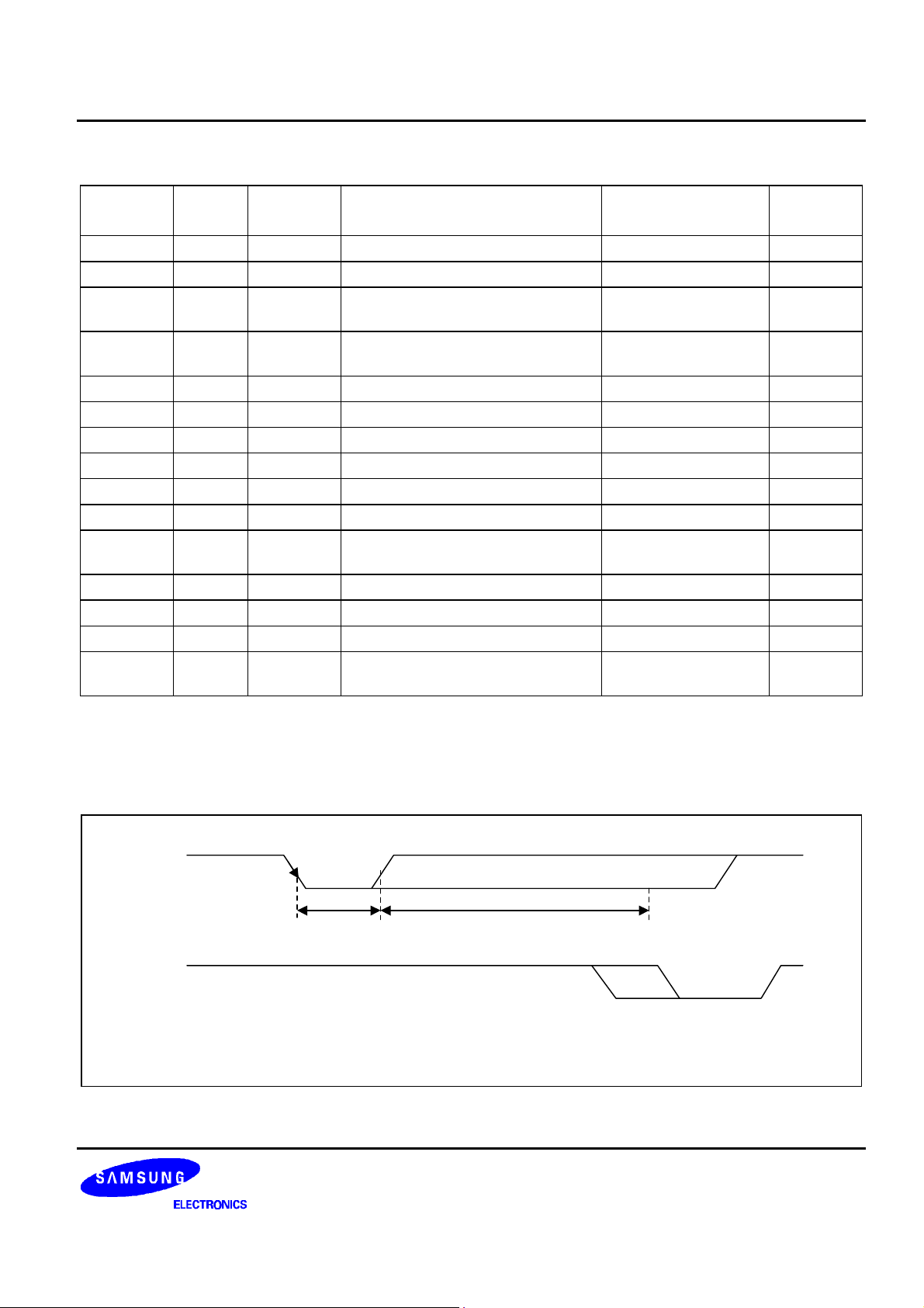
nRESET
64*fMCLK 512*fMCLK
nRSCO
NOTE: After the falling edge of nRESET, the S3C4530A count 64 cycles for a system reset
and needs further 512 cycles for a TAG RAM clear of cache.
After these cycles, the S3C4530A asserts nRCS0 when the nRESET is released.
Figure 1-3. Reset Timing Diagram
1-17
Page 18
PRODUCT OVERVIEW S3C4530A
CPU CORE OVERVIEW
The S3C4530A CPU core is a general purpose 32-bit ARM7TDMI microprocessor, developed by Advanced RISC
Machines, Ltd. (ARM). The core architecture is based on Reduced Instruction Set Computer (RISC) principles.
The RISC architecture makes the instruction set and its related decoding mechanism simpler and more efficient
than those with microprogrammed Complex Instruction Set Computer (CISC) systems. High instruction
throughput and impressive real-time interrupt response are among the major benefits of the architecture.
Pipelining is also employed so that all components of the processing and memory systems can operate
continuously. The ARM7TDMI has a 32-bit address bus.
An important feature of the ARM7TDMI processor that makes itself distinct from the ARM7 processor is a unique
architectural strategy called THUMB. The THUMB strategy is an extension of the basic ARM architecture
consisting of 36 instruction formats. These formats are based on the standard 32-bit ARM instruction set, while
having been re-coded using 16-bit wide opcodes.
As THUMB instructions are one-half the bit width of normal ARM instructions, they produce very high-density
codes. When a THUMB instruction is executed, its 16-bit opcode is decoded by the processor into its equivalent
instruction in the standard ARM instruction set. The ARM core then processes the 16-bit instruction as it would a
normal 32-bit instruction. In other words, the THUMB architecture gives 16-bit systems a way to access the 32-bit
performance of the ARM core without requiring the full overhead of 32-bit processing.
As the ARM7TDMI core can execute both standard 32-bit ARM instructions and 16-bit THUMB instructions, it
allows you to mix the routines of THUMB instructions and ARM code in the same address space. In this way, you
can adjust code size and performance, routine by routine, to find the best programming solution for a specific
application.
Address
Register
Address
Incrementer
Instruction
Register Bank
Multiplier
Barrel
Shifter
32-BIT ALU
Write Data
Register
Decoder and
Logic Controll
Instruction
Pipeline and Read
Data Register
1-18
Figure 1-4. ARM7TDMI Core Block Diagram
Page 19

S3C4530A PRODUCT OVERVIEW
INSTRUCTION SET
The S3C4530A instruction set is divided into two subsets: a standard 32-bit ARM instruction set and a 16-bit
THUMB instruction set.
The 32-bit ARM instruction set is comprised of thirteen basic instruction types, which can, in turn, be divided into
four broad classes:
• Four types of branch instructions which control program execution flow, instruction privilege levels, and
switching between an ARM code and a THUMB code.
• Three types of data processing instructions which use the on-chip ALU, barrel shifter, and multiplier to
perform high-speed data operations in a bank of 31 registers (all with 32-bit register widths).
• Three types of load and store instructions which control data transfer between memory locations and the
registers. One type is optimized for flexible addressing, another for rapid context switching, and the third for
swapping data.
• Three types of co-processor instructions which are dedicated to controlling external co-processors. These
instructions extend the off-chip functionality of the instruction set in an open and uniform way.
NOTE
All 32-bit ARM instructions can be executed conditionally.
The 16-bit THUMB instruction set contains 36 instruction formats drawn from the standard 32-bit ARM instruction
set. The THUMB instructions can be divided into four functional groups:
• Four branch instructions.
• Twelve data processing instructions, which are a subset of the standard ARM data processing instructions.
• Eight load and store register instructions.
• Four load and store multiple instructions.
NOTE
Each 16-bit THUMB instruction has a corresponding 32-bit ARM instruction with an identical processing
model.
The 32-bit ARM instruction set and the 16-bit THUMB instruction set are good targets for compilers of many
different high-level languages. When an assembly code is required for critical code segments, the ARM
programming technique is straightforward, unlike that of some RISC processors which depend on sophisticated
compiler technology to manage complicated instruction interdependencies.
Pipelining is employed so that all parts of the processor and memory systems can operate continuously.
Typically, while one instruction is being executed, its successor is being decoded, and the third instruction is
being fetched from memory.
1-19
Page 20

PRODUCT OVERVIEW S3C4530A
MEMORY INTERFACE
The CPU memory interface has been designed to help the highest performance potential to be realized without
incurring high costs in the memory system. Speed-critical control signals are pipelined so that system control
functions can be implemented in standard low-power logic. These pipelined control signals allow you to fully
exploit the fast local access modes, offered by industry standard dynamic RAMs.
OPERATING STATES
From a programmer′s point of view, the ARM7TDMI core is always in one of two operating states. These states,
which can be switched by software or by exception processing, are:
• ARM state (when executing 32-bit, word-aligned, ARM instructions), and
• THUMB state (when executing 16-bit, half-word aligned THUMB instructions).
OPERATING MODES
The ARM7TDMI core supports seven operating modes:
• User mode: a normal program execution state
• FIQ (Fast Interrupt Request) mode: for supporting a specific data transfer or channel processing
• IRQ (Interrupt Request) mode: for general purpose interrupt handling
• Supervisor mode: a protected mode for the operating system
• Abort mode: entered when a data or instruction pre-fetch is aborted
• System mode: a privileged user mode for the operating system
• Undefined mode: entered when an undefined instruction is executed
Operating mode changes can be controlled by software. They can also be caused by external interrupts or
exception processing. Most application programs execute in user mode. Privileged modes (that is, all modes
other than User mode) are entered to service interrupts or exceptions, or to access protected resources.
1-20
Page 21

S3C4530A PRODUCT OVERVIEW
REGISTERS
The S3C4530A CPU core has a total of 37 registers: 31 general-purpose 32-bit registers, and 6 status registers.
Not all of these registers are always available. Whether a registers is available to the programmer at any given
time depends on the current processor operating state and mode.
NOTE
When the S3C4530A is operating in ARM state, 16 general registers and one or two status registers can
be accessed at any time. In privileged mode, mode-specific banked registers are switched in.
Two register sets, or banks, can also be accessed, depending on the core′s current state, the ARM state register
set and the THUMB state register set:
• The ARM state register set contains 16 directly accessible registers: R0-R15. All of these registers, except for
R15, are for general-purpose use, and can hold either data or address values. An additional (17th) register,
the CPSR (Current Program Status Register), is used to store status information.
• The THUMB state register set is a subset of the ARM state set. You can access 8 general registers, R0-R7,
as well as the program counter (PC), a stack pointer register (SP), a link register (LR), and the CPSR. Each
privileged mode has a corresponding banked stack pointer, link register, and saved process status register
(SPSR).
The THUMB state registers are related to the ARM state registers as follows:
• THUMB state R0-R7 registers and ARM state R0-R7 registers are identical
• THUMB state CPSR and SPSRs and ARM state CPSR and SPSRs are identical
• THUMB state SP, LR, and PC are mapped directly to ARM state registers R13, R14, and R15, respectively
In THUMB state, registers R8-R15 are not part of the standard register set. However, you can access them for
assembly language programming and use them for fast temporary storage, if necessary.
1-21
Page 22
PRODUCT OVERVIEW S3C4530A
EXCEPTIONS
An exception arises when the normal flow of program execution is interrupted, e.g., when processing is diverted
to handle an interrupt from a peripheral. The processor state just prior to handling the exception must be
preserved so that the program flow can be resumed when the exception routine is completed. Multiple exceptions
may arise simultaneously.
To process exceptions, the S3C4530A uses the banked core registers to save the current state. The old PC value
and the CPSR contents are copied into the appropriate R14 (LR) and SPSR registers The PC and mode bits in
the CPSR are adjusted to the value corresponding to the type of exception being processed.
The S3C4530A core supports seven types of exceptions. Each exception has a fixed priority and a corresponding
privileged processor mode, as shown in Table 1-4.
Table 1-4. S3C4530A CPU Exceptions
Exception Mode on Entry Priority
Reset Supervisor mode 1 (highest)
Data abort Abort mode 2
FIQ FIQ mode 3
IRQ IRQ mode 4
Prefetch abort Abort mode 5
Undefined instruction Undefined mode 6
SWI Supervisor mode 6 (lowest)
1-22
Page 23
S3C4530A PRODUCT OVERVIEW
SPECIAL REGISTERS
Table 1-5. S3C4530A Special Registers
Group Registers Offset R/W Description Reset/Value
System SYSCFG 0x0000 R/W System configuration register 0x4FFFFF91
Manager CLKCON 0x3000 R/W Clock control register 0x00000000
EXTACON0 0x3008 R/W External I/O timing register 1 0x00000000
EXTACON1 0x300C R/W External I/O timing register 2 0x00000000
EXTDBWTH 0x3010 R/W Data bus width for each memory bank 0x00000000
ROMCON0 0x3014 R/W ROM/SRAM/Flash bank 0 control register 0x20000060
ROMCON1 0x3018 R/W ROM/SRAM/Flash bank 1 control register 0x00000060
ROMCON2 0x301C R/W ROM/SRAM/Flash bank 2 control register 0x00000060
ROMCON3 0x3020 R/W ROM/SRAM/Flash bank 3 control register 0x00000060
ROMCON4 0x3024 R/W ROM/SRAM/Flash bank 4 control register 0x00000060
ROMCON5 0x3028 R/W ROM/SRAM/Flash bank 5 control register 0x00000060
DRAMCON0 0x302C R/W DRAM bank 0 control register 0x00000000
DRAMCON1 0x3030 R/W DRAM bank 1 control register 0x00000000
DRAMCON2 0x3034 R/W DRAM bank 2 control register 0x00000000
DRAMCON3 0x3038 R/W DRAM bank 3 control register 0x00000000
REFEXTCON 0x303C R/W Refresh and external I/O control register 0x000083ED
Ethernet BDMATXCON 0x9000 R/W Buffered DMA receive control register 0x00000000
(BDMA) BDMARXCON 0x9004 R/W Buffered DMA transmit control register 0x00000000
BDMATXPTR 0x9008 R/W Transmit frame descriptor start address 0x00000000
BDMARXPTR 0x900C R/W Receive frame descriptor start address 0x00000000
BDMARXLSZ 0x9010 R/W Receive frame maximum size Undefined
BDMASTAT 0x9014 R/W Buffered DMA status 0x00000000
CAM 0x9100-
0x917C
BDMATXBUF 0x9200-
0x92FC
BDMARXBUF 0x9800-
0x99FC
Ethernet MACON 0xA000 R/W Ethernet MAC control register 0x00000000
(MAC) CAMCON 0xA004 R/W CAM control register 0x00000000
MACTXCON 0xA008 R/W MAC transmit control register 0x00000000
MACTXSTAT 0xA00C R/W MAC transmit status register 0x00000000
MACRXCON 0xA010 R/W MAC receive control register 0x00000000
MACRXSTAT 0xA014 R/W MAC receive status register 0x00000000
W CAM content (32 words) Undefined
R/W BDMA Tx buffer (64 words) for test mode
addressing
R/W BDMA Rx buffer (64 words) for test mode
addressing
Undefined
Undefined
1-23
Page 24
PRODUCT OVERVIEW S3C4530A
Table 1-5. S3C4530A Special Registers (Continued)
Group Registers Offset R/W Description Reset/Value
Ethernet STADATA 0xA018 R/W Station management data 0x00000000
(MAC) STACON 0xA01C R/W Station management control and address 0x00006000
CAMEN 0xA028 R/W CAM enable register 0x00000000
EMISSCNT 0xA03C R/W Missed error count register 0x00000000
EPZCNT 0xA040 R Pause count register 0x00000000
ERMPZCNT 0xA044 R Remote pause count register 0x00000000
ETXSTAT 0x9040 R Transmit control frame status 0x00000000
HDLC HMODE 0x7000 R/W HDLC mode register 0x00000000
Channel A HCON 0x7004 R/W HDLC control register 0x00000000
HSTAT 0x7008 R/W HDLC status register 0x00010400
HINTEN 0x700C R/W HDLC interrupt enable register 0x00000000
HTXFIFOC 0x7010 W TxFIFO frame continue register -
HTXFIFOT 0x7014 W TxFIFO frame terminate register -
HRXFIFO 0x7018 R HDLC RxFIFO entry register 0x00000000
HBRGTC 0x701C R/W HDLC baud rate generate time constant 0x00000000
HPRMB 0x7020 R/W HDLC preamble constant 0x00000000
HSAR0 0x7024 R/W HDLC station address 0 0x00000000
HSAR1 0x7028 R/W HDLC station address 1 0x00000000
HSAR2 0x702C R/W HDLC station address 2 0x00000000
HSAR3 0x7030 R/W HDLC station address 3 0x00000000
HMASK 0x7034 R/W HDLC mask register 0x00000000
HDMATxPTR 0x7038 R/W DMA Tx buffer descriptor pointer 0x00000000
HDMARxPTR 0x703C R/W DMA Rx buffer descriptor pointer 0x00000000
HMFLR 0x7040 R/W Maximum frame length register 0x00000000
HRBSR 0x7040 R/W DMA receive buffer size register 0x00000000
HSYNC 0x7048 R/W HDLC Sync Register 0x7E
TCON 0x704C R/W Transparent Control Register 0x00000000
HDLC HMODE 0x8000 R/W HDLC mode register 0x00000000
Channel B HCON 0x8004 R/W HDLC control register 0x00000000
HSTAT 0x8008 R/W HDLC status register 0x00010400
HINTEN 0x800C R/W HDLC interrupt enable register 0x00000000
HTXFIFOC 0x8010 W TxFIFO frame continue register 0x00000000
HTXFIFOT 0x8014 W TxFIFO frame terminate register 0x00000000
HRXFIFO 0x8018 R HDLC RxFIFO entry register 0x00000000
HBRGTC 0x801C R/W HDLC baud rate generate time constant 0x00000000
HPRMB 0x8020 R/W HDLC preamble constant 0x00000000
1-24
Page 25
S3C4530A PRODUCT OVERVIEW
Table 1-5. S3C4530A Special Registers (Continued)
Group Registers Offset R/W Description Reset/Value
HDLC HSAR0 0x8024 R/W HDLC station address 0 0x00006000
Channel B HSAR1 0x8028 R/W HDLC station address 1 0x00000000
HSAR2 0x802C R/W HDLC station address 2 0x00000000
HSAR3 0x8030 R HDLC station address 3 0x00000000
HMASK 0x8034 R HDLC mask register 0x00000000
HDMATxPTR 0x8038 R DMA Tx buffer descriptor pointer 0x00000000
HDMARxPTR 0x803C R/W DMA Rx buffer descriptor pointer 0x00000000
HMFLR 0x8040 R/W Maximum frame length register 0x00000000
HRBSR 0x8044 R/W DMA receive buffer size register 0x00000000
HSYNC 0x8048 R/W HDLC Sync Register 0x7E
TCON 0x804C R/W Transparent Control Register 0x00000000
I/O Ports IOPMOD 0x5000 R/W I/O port mode register 0x00000000
IOPCON 0x5004 R/W I/O port control register 0x00000000
IOPDATA 0x5008 R/W Input port data register 0x00000000
Interrupt INTMOD 0x4000 R/W Interrupt mode register Undefined
Controller INTPND 0x4004 R/W Interrupt pending register 0x00000000
INTMSK 0x4008 R/W Interrupt mask register 0x00000000
INTPRI0 0x400C R/W Interrupt priority register 0 0x003FFFFF
INTPRI1 0x4010 R/W Interrupt priority register 1 0x07060504
INTPRI2 0x4014 R/W Interrupt priority register 2 0x0B0A0908
INTPRI3 0x4018 R/W Interrupt priority register 3 0x0F0E0D0C
INTPRI4 0x401C R/W Interrupt priority register 4 0x13121110
INTPRI5 0x4020 R/W Interrupt priority register 5 0x00000014
INTOFFSET 0x4024 R Interrupt offset address register 0x00000054
INTOSET_FIQ 0x4030 R FIQ interrupt offset register 0x00000054
INTOSET_IRQ 0x4034 R IRQ interrupt offset register 0x00000054
I2C Bus IICCON 0XF000 R/W I2C bus control status register 0x00000054
IICBUF 0xF004 R/W I2C bus shift buffer register Undefined
IICPS 0xF008 R/W I2C bus prescaler register 0x00000000
IICCOUNT 0xF00C R I2C bus prescaler counter register 0x00000000
GDMA GDMACON0 0xB000 R/W GDMA channel 0 control register 0x00000000
GDMACON1 0xC000 R/W GDMA channel 1 control register 0x00000000
GDMASRC0 0xB004 R/W GDMA source address register 0 Undefined
GDMADST0 0xB008 R/W GDMA destination address register 0 Undefined
1-25
Page 26
PRODUCT OVERVIEW S3C4530A
Table 1-5. S3C4530AC Special Registers (Continued)
Group Registers Offset R/W Description Reset/Value
GDMA GDMASRC1 0xC004 R/W GDMA source address register 1 Undefined
GDMADST1 0xC008 R/W GDMA destination address register 1 Undefined
GDMACNT0 0xB00C R/W GDMA channel 0 transfer count register Undefined
GDMACNT1 0xC00C R/W GDMA channel 1 transfer count register Undefined
UART UCON0 0xD000 R/W UART channel 0 control register 0x00
UCON1 0xE000 R/W UART channel 1 control register 0x00
USTAT0 0xD004 R/W UART channel 0 status register 0xE0240
USTAT1 0xE004 R/W UART channel 1 status register 0xE0240
UINTEN0 0xD008 R/W UART channel 0 interrupt enable register 0x00000000
UINTEN1 0xE008 R/W UART channel 1 interrupt enable register 0x00000000
UTXBUF0 0xD00C W UART channel 0 transmit holding register Undefined
UTXBUF1 0xE00C W UART channel 1 transmit holding register Undefined
URXBUF0 0xD010 R UART channel 0 receive buffer register Undefined
URXBUF1 0xE010 R UART channel 1 receive buffer register Undefined
UBRDIV0 0xD014 R/W Baud rate divisor register 0 0x00
UBRDIV1 0xE014 R/W Baud rate divisor register 1 0x00
UCC1_0 0xD018 R/W UART0 Control Character Register 1 0x00000000
UCC1_1 0xE018 R/W UART1 Control Character Register 1 0x00000000
UCC2_0 0xD01C R/W UART0 Control Character Register 2 0x00000000
UCC2_1 0xE01C R/W UART1 Control Character Register 2 0x00000000
Timers TMOD 0x6000 R/W Timer mode register 0x00000000
TDATA0 0x6004 R/W Timer 0 data register 0x00000000
TDATA1 0x6008 R/W Timer 1 data register 0x00000000
TCNT0 0x600C R/W Timer 0 count register 0xffffffff
TCNT1 0x6010 R/W Timer 1 count register 0xffffffff
1-26
Page 27

S3C4530A PROGRAMMER'S MODEL
2 PROGRAMMER′′S MODEL
OVERVIEW
S3C4530A was developed using the advanced ARM7TDMI core designed by advanced RISC machines, Ltd.
Processor Operating States
From the programmer′s point of view, the ARM7TDMI can be in one of two states:
— ARM state which executes 32-bit, word-aligned ARM instructions.
— THUMB state which operates with 16-bit, half-word-aligned THUMB instructions. In this state, the PC uses bit
1 to select between alternate half-words.
NOTE
Transition between these two states does not affect the processor mode or the contents of the registers.
SWITCHING STATE
Entering THUMB State
Entry into THUMB state can be achieved by executing a BX instruction with the state bit (bit 0) set in the operand
register.
Transition to THUMB state will also occur automatically on return from an exception (IRQ, FIQ, UNDEF, ABORT,
SWI etc.), if the exception was entered with the processor in THUMB state.
Entering ARM State
Entry into ARM state happens:
1. On execution of the BX instruction with the state bit clear in the operand register.
2. On the processor taking an exception (IRQ, FIQ, RESET, UNDEF, ABORT, SWI etc.). In this case, the PC is
placed in the exception mode′s link register, and execution commences at the exception′s vector address.
MEMORY FORMATS
ARM7TDMI views memory as a linear collection of bytes numbered upwards from zero. Bytes 0 to 3 hold the first
stored word, bytes 4 to 7 the second and so on. ARM7TDMI can treat words in memory as being stored either in
Big-Endian or Little-Endian format.
2-1
Page 28
PROGRAMMER'S MODEL S3C4530A
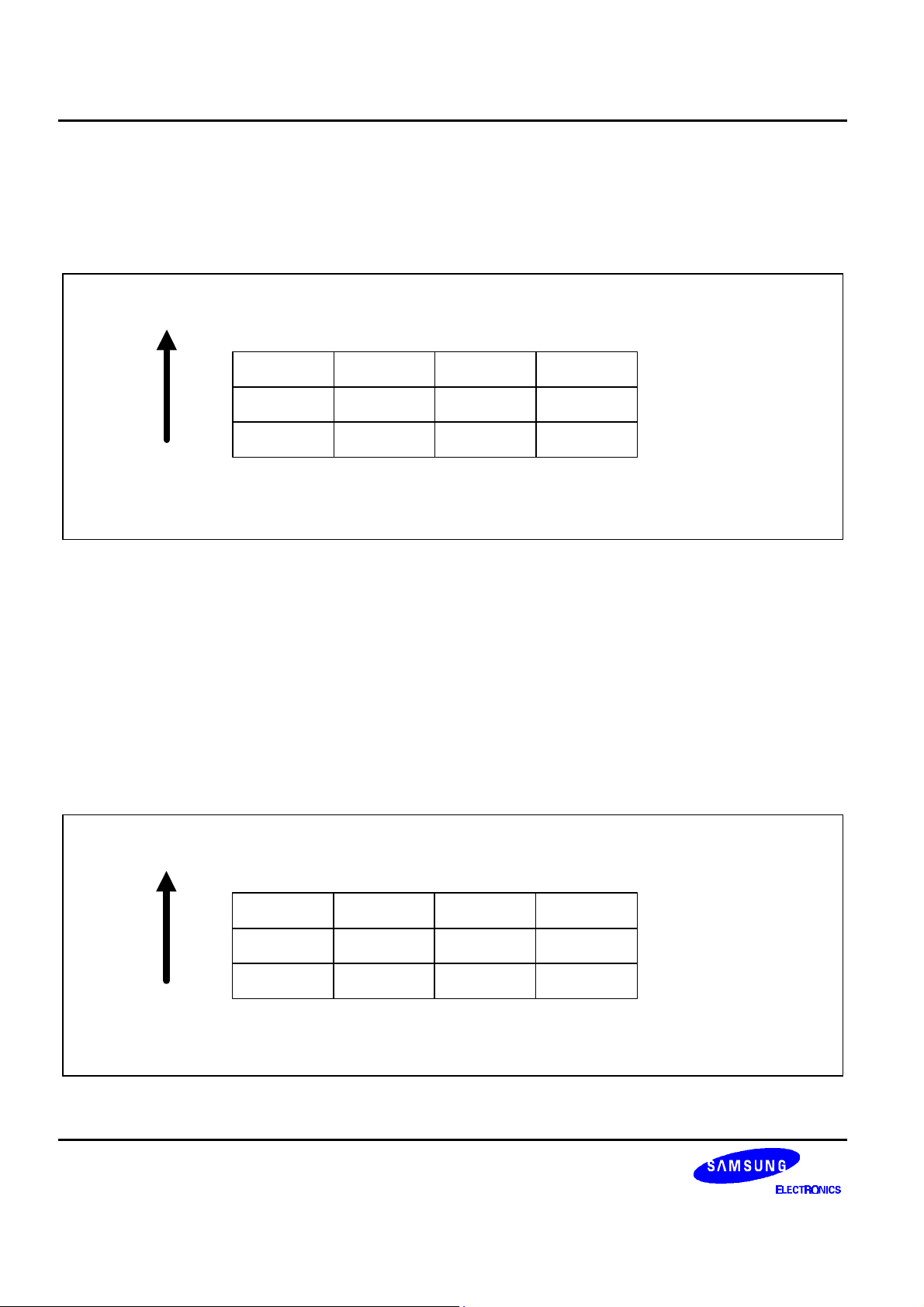
BIG-ENDIAN FORMAT
In Big-Endian format, the most significant byte of a word is stored at the lowest numbered byte and the least
significant byte at the highest numbered byte. Byte 0 of the memory system is therefore connected to data lines
31 through 24.
Higher address
Lower address
31
24
8
4
0
w Most significant byte is at lowest address
w Word is addressed by byte address of most signficant byte
9 15 8 7 0 Word address
5
9
5
1
10
11
6
2
7
3
8
4
0
Figure 2-1. Big-Endian Addresses of Bytes within Words
NOTE
The data locations in the external memory are different with Figure 2-1 in the S3C4620. Please refer to
the chapter 4, system manager.
LITTLE-ENDIAN FORMAT
In Little-Endian format, the lowest numbered byte in a word is considered the word′s least significant byte, and
the highest numbered byte the most significant. Byte 0 of the memory system is therefore connected to data lines
7 through 0.
2-2
Higher address
Lower address
31
24
11
7
3
w Most significant byte is at lowest address
w Word is addressed by byte address of least signficant byte
23 15 8 7 0
16
10
6
2
9
5
1
8
4
0
Figure 2-2. Little-Endian Addresses of Bytes Words
Word address
8
4
0
Page 29

S3C4530A PROGRAMMER'S MODEL
INSTRUCTION LENGTH
Instructions are either 32 bits long (in ARM state) or 16 bits long (in THUMB state).
Data Types
ARM7TDMI supports byte (8-bit), half-word (16-bit) and word (32-bit) data types. Words must be aligned to fourbyte boundaries and half words to two-byte boundaries.
OPERATING MODES
ARM7TDMI supports seven modes of operation:
— User (usr): The normal ARM program execution state
— FIQ (fiq): Designed to support a data transfer or channel process
— IRQ (irq): Used for general-purpose interrupt handling
— Supervisor (svc): Protected mode for the operating system
— Abort mode (abt): Entered after a data or instruction prefetch abort
— System (sys): A privileged user mode for the operating system
— Undefined (und): Entered when an undefined instruction is executed
Mode changes may be made under software control, or may be brought about by external interrupts or exception
processing. Most application programs will execute in User mode. The non-user modes known as privileged
modes-are entered in order to service interrupts or exceptions, or to access protected resources.
2-3
Page 30

PROGRAMMER'S MODEL S3C4530A
REGISTERS
ARM7TDMI has a total of 37 registers-31 general-purpose 32-bit registers and six status registers - but these
cannot all be seen at once. The processor state and operating mode dictate which registers are available to the
programmer.
The ARM State Register Set
In ARM state, 16 general registers and one or two status registers are visible at any one time. In privileged (nonUser) modes, mode-specific banked registers are switched in. Figure 2-3 shows which registers are available in
each mode: the banked registers are marked with a shaded triangle.
The ARM state register set contains 16 directly accessible registers: R0 to R15. All of these except R15 are
general-purpose, and may be used to hold either data or address values. In addition to these, there is a
seventeenth register used to store status information.
Register 14 is used as the subroutine link register. This receives a copy of R15 when a branch
and link (BL) instruction is executed. At all other times it may be treated as a
general-purpose register. The corresponding banked registers R14_svc, R14_irq,
R14_fiq, R14_abt and R14_und are similarly used to hold the return values of
R15 when interrupts and exceptions arise, or when branch and link instructions are
executed within interrupt or exception routines.
Register 15
holds the Program Counter (PC). In ARM state, bits [1:0] of R15 are zero and bits
[31:2] contain the PC. In THUMB state, bit [0] is zero and bits [31:1] contain the PC.
Register 16
is the CPSR (Current Program Status Register). This contains condition code flags
and the current mode bits.
FIQ mode has seven banked registers mapped to R8-14 (R8_fiq-R14_fiq). In ARM state, many FIQ handlers do
not need to save any registers. User, IRQ, Supervisor, Abort and Undefined each have two banked registers
mapped to R13 and R14, allowing each of these modes to have a private stack pointer and link registers.
2-4
Page 31

S3C4530A PROGRAMMER'S MODEL
ARM State General Registers and Program Counter
System & User FIQ Supervisor About IRG Undefined
R0
R1
R2
R3
R4
R5
R6
R7
R8
R9
R10
R11
R12
R13
R14
R15 (PC)
CPSR CPSR
R0
R1
R2
R3
R4
R5
R6
R7
R8_fiq
R9_fiq
R10_fiq
R11_fiq
R12_fiq
R13_fiq
R14_fiq
R15 (PC)
SPSR_fiq
R0
R1
R2
R3
R4
R5
R6
R7
R8
R9
R10
R11
R12
R13_svc
R14_svc
R15 (PC)
ARM State Program Status Register
CPSR
SPSR_svc
R0
R1
R2
R3
R4
R5
R6
R7
R8
R9
R10
R11
R12
R13_abt
R14_abt
R15 (PC)
CPSR
SPSR_abt
R0
R1
R2
R3
R4
R5
R6
R7
R8
R9
R10
R11
R12
R13_irq
R14_irq
R15 (PC)
CPSR
SPSR_irq
R0
R1
R2
R3
R4
R5
R6
R7
R8
R9
R10
R11
R12
R13_und
R14_und
R15 (PC)
CPSR
SPSR_und
= banked register
Figure 2-3. Register Organization in ARM State
2-5
Page 32

PROGRAMMER'S MODEL S3C4530A
The THUMB State Register Set
The THUMB state register set is a subset of the ARM state set. The programmer has direct access to eight
general registers, R0–R7, as well as the Program Counter (PC), a stack pointer register (SP), a link register (LR),
and the CPSR. There are banked stack pointers, link registers and Saved Process Status Registers (SPSRs) for
each privileged mode. This is shown in Figure 2-4.
THUMB State General Registers and Program Counter
System & User FIQ Supervisor About IRG Undefined
R0
R1
R2
R3
R4
R5
R6
R7
SP
LR
PC
CPSR CPSR
= banked register
R0
R1
R2
R3
R4
R5
R6
R7
SP_fiq
LR_fiq
PC
SPSR_fiq
Figure 2-4. Register Organization in THUMB State
R0
R1
R2
R3
R4
R5
R6
R7
SP_svg
LR_svc
PC
THUMB State Program Status Registers
CPSR
SPSR_svc
R0
R1
R2
R3
R4
R5
R6
R7
SP_abt
LR_abt
PC
CPSR
SPSR_abt
R0
R1
R2
R3
R4
R5
R6
R7
SP_irq
LR_irq
PC
CPSR
SPSR_irq
R0
R1
R2
R3
R4
R5
R6
R7
SP_und
LR_und
PC
CPSR
SPSR_und
2-6
Page 33

S3C4530A PROGRAMMER'S MODEL
Lo-registersHi-registers
The Relationship between ARM and THUMB State Registers
The THUMB state registers relate to the ARM state registers in the following way:
— THUMB state R0–R7 and ARM state R0–R7 are identical
— THUMB state CPSR and SPSRs and ARM state CPSR and SPSRs are identical
— THUMB state SP maps onto ARM state R13
— THUMB state LR maps onto ARM state R14
— The THUMB state program counter maps onto the ARM state program counter (R15)
This relationship is shown in Figure 2-5.
THUMB State ARM State
R0
R1
R2
R3
R4
R5
R6
R7
Stack Pointer (SP)
Link Register (LR)
Program Counter (PC)
CPSR
SPSR
Stack Pointer (R13)
Link Register (R14)
Program Counter (R15)
R0
R1
R2
R3
R4
R5
R6
R7
R8
R9
R10
R11
R12
CPSR
SPSR
Figure 2-5. Mapping of THUMB State Registers onto ARM State Registers
2-7
Page 34

PROGRAMMER'S MODEL S3C4530A
Accessing Hi-Registers in THUMB State
In THUMB state, registers R8–R15 (the Hi registers) are not part of the standard register set. However, the
assembly language programmer has limited access to them, and can use them for fast temporary storage.
A value may be transferred from a register in the range R0–R7 (a Lo register) to a Hi register, and from a Hi
register to a Lo register, using special variants of the MOV instruction. Hi register values can also be compared
against or added to Lo register values with the CMP and ADD instructions. For more information, refer to Figure
3-34.
THE PROGRAM STATUS REGISTERS
The ARM7TDMI contains a Current Program Status Register (CPSR), plus five Saved Program Status Registers
(SPSRs) for use by exception handlers. These register′s functions are:
— Hold information about the most recently performed ALU operation
— Control the enabling and disabling of interrupts
— Set the processor operating mode
The arrangement of bits is shown in Figure 2-6.
Condition Code Flags (Reserved)
31 30 29 28 27 26 25 24 8 7 6 5 4 3 2 1 0
N Z C V . . .. . . I F T M4 M3 M2 M1 M0
Overflow
Carry/Borrow/Extend
Zero
Negative/Less Than
Control Bits
Mode bits
State bit
FIQ disable
FRQ disable
Figure 2-6. Program Status Register Format
2-8
Page 35

S3C4530A PROGRAMMER'S MODEL
The Condition Code Flags
The N, Z, C and V bits are the condition code flags. These may be changed as a result of arithmetic and logical
operations, and may be tested to determine whether an instruction should be executed.
In ARM state, all instructions may be executed conditionally: see Table 3-2 for details.
In THUMB state, only the branch instruction is capable of conditional execution: see Figure 3-46 for details.
The Control Bits
The bottom 8 bits of a PSR (incorporating I, F, T and M[4:0]) are known collectively as the control bits. These will
change when an exception arises. If the processor is operating in a privileged mode, they can also be
manipulated by software.
The T bit This reflects the operating state. When this bit is set, the processor is executing in
THUMB state, otherwise it is executing in ARM state. This is reflected on the TBIT
external signal.
Note that the software must never change the state of the TBIT in the CPSR. If this
happens, the processor will enter an unpredictable state.
Interrupt disable bits
The I and F bits are the interrupt disable bits. When set, these disable the IRQ and
FIQ interrupts respectively.
The mode bits
The M4, M3, M2, M1 and M0 bits (M[4:0]) are the mode bits. These determine the
processor′s operating mode, as shown in Table 2-1. Not all combinations of the
mode bits define a valid processor mode. Only those explicitly described shall be
used. The user should be aware that if any illegal value is programmed into the
mode bits, M[4:0], then the processor will enter an unrecoverable state. If this
occurs, reset should be applied.
2-9
Page 36

PROGRAMMER'S MODEL S3C4530A
Table 2-1. PSR Mode. Bit Values
M[4:0] Mode Visible THUMB State Registers Visible ARM State Registers
10000 User R7..R0,
LR, SP
R14..R0,
PC, CPSR
PC, CPSR
10001 FIQ R7..R0,
LR_fiq, SP_fiq
PC, CPSR, SPSR_fiq
10010 IRQ R7..R0,
LR_irq, SP_irq
PC, CPSR, SPSR_irq
10011 Supervisor R7..R0,
LR_svc, SP_svc,
PC, CPSR, SPSR_svc
10111 Abort R7..R0,
LR_abt, SP_abt,
PC, CPSR, SPSR_abt
11011 Undefined R7..R0
LR_und, SP_und,
PC, CPSR, SPSR_und
11111 System R7..R0,
LR, SP
R7..R0,
R14_fiq..R8_fiq,
PC, CPSR, SPSR_fiq
R12..R0,
R14_irq..R13_irq,
PC, CPSR, SPSR_irq
R12..R0,
R14_svc..R13_svc,
PC, CPSR, SPSR_svc
R12..R0,
R14_abt..R13_abt,
PC, CPSR, SPSR_abt
R12..R0,
R14_und..R13_und,
PC, CPSR
R14..R0,
PC, CPSR
PC, CPSR
Reserved bits
2-10
The remaining bits in the PSRs are reserved. When changing a PSR′s flag or
control bits, you must ensure that these unused bits are not altered. Also, your
program should not rely on them containing specific values, since in future
processors they may read as one or zero.
Page 37

S3C4530A PROGRAMMER'S MODEL
EXCEPTIONS
Exceptions arise whenever the normal flow of a program has to be halted temporarily, for example to service an
interrupt from a peripheral. Before an exception can be handled, the current processor state must be preserved
so that the original program can resume when the handler routine has finished.
It is possible for several exceptions to arise at the same time. If this happens, they are dealt with in a fixed order.
See Exception Priorities on page 2-14.
Action on Entering an Exception
When handling an exception, the ARM7TDMI:
1. Preserves the address of the next instruction in the appropriate Link Register. If the exception has been
entered from ARM state, then the address of the next instruction is copied into the Link Register (that is,
current PC + 4 or PC + 8 depending on the exception. See Table 2-2 on for details). If the exception has
been entered from THUMB state, then the value written into the Link Register is the current PC offset by a
value such that the program resumes from the correct place on return from the exception. This means that
the exception handler need not determine which state the exception was entered from. For example, in the
case of SWI, MOVS PC, R14_svc will always return to the next instruction regardless of whether the SWI
was executed in ARM or THUMB state.
2. Copies the CPSR into the appropriate SPSR
3. Forces the CPSR mode bits to a value which depends on the exception
4. Forces the PC to fetch the next instruction from the relevant exception vector
It may also set the interrupt disable flags to prevent otherwise unmanageable nesting of exceptions.
If the processor is in THUMB state when an exception occurs, it will automatically switch into ARM state when the
PC is loaded with the exception vector address.
Action on Leaving an Exception
On completion, the exception handler:
1. Moves the Link Register, minus an offset where appropriate, to the PC. (The offset will vary depending on the
type of exception.)
2. Copies the SPSR back to the CPSR
3. Clears the interrupt disable flags, if they were set on entry
NOTE
An explicit switch back to THUMB state is never needed, since restoring the CPSR from the SPSR
automatically sets the T bit to the value it held immediately prior to the exception.
2-11
Page 38

PROGRAMMER'S MODEL S3C4530A
Exception Entry/Exit Summary
Table 2-2 summarizes the PC value preserved in the relevant R14 on exception entry, and the recommended
instruction for exiting the exception handler.
Table 2-2. Exception Entry/Exit
Return Instruction Previous State Notes
ARM R14_x THUMB R14_x
BL MOV PC, R14 PC + 4 PC + 2 1
SWI MOVS PC, R14_svc PC + 4 PC + 2 1
UDEF MOVS PC, R14_und PC + 4 PC + 2 1
FIQ SUBS PC, R14_fiq, #4 PC + 4 PC + 4 2
IRQ SUBS PC, R14_irq, #4 PC + 4 PC + 4 2
PABT SUBS PC, R14_abt, #4 PC + 4 PC + 4 1
DABT SUBS PC, R14_abt, #8 PC + 8 PC + 8 3
RESET NA – – 4
NOTES:
1. Where PC is the address of the BL/SWI/Undefined Instruction fetch which had the prefetch abort.
2. Where PC is the address of the instruction which did not get executed since the FIQ or IRQ took priority.
3. Where PC is the address of the Load or Store instruction which generated the data abort.
4. The value saved in R14_svc upon reset is unpredictable.
FIQ
The FIQ (Fast Interrupt Request) exception is designed to support a data transfer or channel process, and in
ARM state has sufficient private registers to remove the need for register saving (thus minimizing the overhead
of context switching).
FIQ is externally generated by taking the nFIQ input LOW. This input can except either synchronous or
asynchronous transitions, depending on the state of the ISYNC input signal. When ISYNC is LOW, nFIQ and
nIRQ are considered asynchronous, and a cycle delay for synchronization is incurred before the interrupt can
affect the processor flow.
Irrespective of whether the exception was entered from ARM or Thumb state, a FIQ handler should leave the
interrupt by executing
SUBS PC,R14_fiq,#4
FIQ may be disabled by setting the CPSR's F flag (but note that this is not possible from User mode). If the F flag
is clear, ARM7TDMI checks for a LOW level on the output of the FIQ synchroniser at the end of each instruction.
2-12
Page 39

S3C4530A PROGRAMMER'S MODEL
IRQ
The IRQ (Interrupt Request) exception is a normal interrupt caused by a LOW level on the nIRQ input. IRQ has a
lower priority than FIQ and is masked out when a FIQ sequence is entered. It may be disabled at any time by
setting the I bit in the CPSR, though this can only be done from a privileged (non-User) mode.
Irrespective of whether the exception was entered from ARM or Thumb state, an IRQ handler should return from
the interrupt by executing
SUBS PC,R14_irq,#4
Abort
An abort indicates that the current memory access cannot be completed. It can be signalled by the external
ABORT input. ARM7TDMI checks for the abort exception during memory access cycles.
There are two types of abort:
— Prefetch abort: occurs during an instruction prefetch.
— Data abort: occurs during a data access.
If a prefetch abort occurs, the prefetched instruction is marked as invalid, but the exception will not be taken until
the instruction reaches the head of the pipeline. If the instruction is not executed - for example because a branch
occurs while it is in the pipeline - the abort does not take place.
If a data abort occurs, the action taken depends on the instruction type:
— Single data transfer instructions (LDR, STR) write back modified base registers: the Abort handler must be
aware of this.
— The swap instruction (SWP) is aborted as though it had not been executed.
— Block data transfer instructions (LDM, STM) complete. If write-back is set, the base is updated. If the
instruction would have overwritten the base with data (ie it has the base in the transfer list), the overwriting is
prevented. All register overwriting is prevented after an abort is indicated, which means in particular that R15
(always the last register to be transferred) is preserved in an aborted LDM instruction.
The abort mechanism allows the implementation of a demand paged virtual memory system. In such a system
the processor is allowed to generate arbitrary addresses. When the data at an address is unavailable, the
Memory Management Unit (MMU) signals an abort. The abort handler must then work out the cause of the abort,
make the requested data available, and retry the aborted instruction. The application program needs no
knowledge of the amount of memory available to it, nor is its state in any way affected by the abort.
After fixing the reason for the abort, the handler should execute the following irrespective of the state (ARM or
Thumb):
SUBS PC,R14_abt,#4 ; for a prefetch abort, or
SUBS PC,R14_abt,#8 ; for a data abort
This restores both the PC and the CPSR, and retries the aborted instruction.
2-13
Page 40

PROGRAMMER'S MODEL S3C4530A
Software Interrupt
The software interrupt instruction (SWI) is used for entering Supervisor mode, usually to request a particular
supervisor function. A SWI handler should return by executing the following irrespective of the state (ARM or
Thumb):
MOV PC,R14_svc
This restores the PC and CPSR, and returns to the instruction following the SWI.
NOTE
nFIQ, nIRQ, ISYNC, LOCK, BIGEND, and ABORT pins exist only in the ARM7TDMI CPU core.
Undefined Instruction
When ARM7TDMI comes across an instruction which it cannot handle, it takes the undefined instruction trap.
This mechanism may be used to extend either the THUMB or ARM instruction set by software emulation.
After emulating the failed instruction, the trap handler should execute the following irrespective of the state (ARM
or Thumb):
MOVS PC,R14_und
This restores the CPSR and returns to the instruction following the undefined instruction.
Exception Vectors
The following table shows the exception vector addresses.
Table 2-3. Exception Vectors
Address Exception Mode in Entry
0x00000000 Reset Supervisor
0x00000004 Undefined instruction Undefined
0x00000008 Software Interrupt Supervisor
0x0000000C Abort (prefetch) Abort
0x00000010 Abort (data) Abort
0x00000014 Reserved Reserved
0x00000018 IRQ IRQ
0x0000001C FIQ FIQ
2-14
Page 41

S3C4530A PROGRAMMER′′S MODEL
Exception Priorities
When multiple exceptions arise at the same time, a fixed priority system determines the order in which they are
handled:
Highest priority:
1. Reset
2. Data abort
3. FIQ
4. IRQ
5. Prefetch abort
Lowest priority:
6. Undefined Instruction, Software interrupt.
Not All Exceptions Can Occur at Once:
Undefined Instruction and Software Interrupt are mutually exclusive, since they each correspond to particular
(non-overlapping) decoding of the current instruction.
If a data abort occurs at the same time as a FIQ, and FIQs are enabled (ie the CPSR's F flag is clear),
ARM7TDMI enters the data abort handler and then immediately proceeds to the FIQ vector. A normal return from
FIQ will cause the data abort handler to resume execution. Placing data abort at a higher priority than FIQ is
necessary to ensure that the transfer error does not escape detection. The time for this exception entry should be
added to worst-case FIQ latency calculations.
2-15
Page 42

PROGRAMMER′′S MODEL S3C4530A
Interrupt Latencies
The worst case latency for FIQ, assuming that it is enabled, consists of the longest time the request can take to
pass through the synchroniser (Tsyncmax if asynchronous), plus the time for the longest instruction to complete
(Tldm, the longest instruction is an LDM which loads all the registers including the PC), plus the time for the data
abort entry (Texc), plus the time for FIQ entry (Tfiq). At the end of this time ARM7TDMI will be executing the
instruction at 0x1C.
Tsyncmax is 3 processor cycles, Tldm is 20 cycles, Texc is 3 cycles, and Tfiq is 2 cycles. The total time is
therefore 28 processor cycles. This is just over 1.4 microseconds in a system which uses a continuous 20 MHz
processor clock. The maximum IRQ latency calculation is similar, but must allow for the fact that FIQ has higher
priority and could delay entry into the IRQ handling routine for an arbitrary length of time. The minimum latency
for FIQ or IRQ consists of the shortest time the request can take through the synchroniser (Tsyncmin) plus Tfiq.
This is 4 processor cycles.
Reset
When the nRESET signal goes LOW, ARM7TDMI abandons the executing instruction and then continues to fetch
instructions from incrementing word addresses.
When nRESET goes HIGH again, ARM7TDMI:
1. Overwrites R14_svc and SPSR_svc by copying the current values of the PC and CPSR into them. The value
of the saved PC and SPSR is not defined.
2. Forces M[4:0] to 10011 (Supervisor mode), sets the I and F bits in the CPSR, and clears the CPSR's T bit.
3. Forces the PC to fetch the next instruction from address 0x00.
4. Execution resumes in ARM state.
2-16
Page 43

S3C4530A INSTRUCTION SET
3 INSTRUCTION SET
INSTRUCTION SET SUMMAY
This chapter describes the ARM instruction set and the THUMB instruction set in the ARM7TDMI core.
FORMAT SUMMARY
The ARM instruction set formats are shown below.
31 30 29 28 27 26 25 24 23 22 21 20 19 18 17 16 15 14 13 12 11 10 9 8 7 6 5 4 3 2 1 0
Cond 0 0 1 Opcode S Rn Rd Operand2
Cond 0 0 0 0 0 0 A S Rd Rn Rs 1 0 0 1 Rm
Data processing/
PSR Transfer
Multiply
Cond 0 0 0 0 1 U A S RdHi RnLo Rn 1 0 0 1 Rm
Cond 0 0 0 1 0 B 0 0 Rn Rd Rm0 0 0 0 1 0 0 1
Cond 0 0 0 1 0 0 1 0 1 1 1 1 1 1 1 1 1 1 1 1 0 0 0 1 Rn
Cond 0 0 0 P U 0 W L Rn Rd 0 0 0 0 1 S H 1 Rm
Cond 0 0 0 P U 1 W L Rn Rd Offset 1 S H 1 Offset
Cond 0 1 1 P U B W L Rn Rd Offset
Cond 0 1 1 1
Cond 1 0 0 P U S W L Rn Register List
Cond 1 0 1 L Offset
Cond 1 1 0 P U N W L Rn CRd CP# Offset
Cond 1 1 1 0 CRn CRdCP Opc CP# CP# 0 CRm
Cond 1 1 1 0 CRn RdCP Opc L CP# CP# 1 CRm
Cond 1 1 1 1 Ignored by processor
31 30 29 28 27 26 25 24 23 22 21 20 19 18 17 16 15 14 13 12 11 10 9 8 7 6 5 4 3 2 1 0
Figure 3-1. ARM Instruction Set Format
NOTE
Multiply Long
Single data swap
Branch and exchange
Halfword data transfer:
register offset
Halfword data transfer:
immediate offset
Single data transfer
Undefined
Block data transfer
Branch
Coprocessor data
transfer
Coprocessor data
Operation
Coprocessor register
Transfer
Software Interrupt
Some instruction codes are not defined but do not cause the Undefined instruction trap to be taken, for
instance a Multiply instruction with bit 6 changed to a 1. These instructions should not be used, as their
action may change in future ARM implementations.
3-1
Page 44

INSTRUCTION SET S3C4530A
INSTRUCTION SUMMARY
Table 3-1. The ARM Instruction Set
Mnemonic Instruction Action
ADC Add with carry Rd: = Rn + Op2 + Carry
ADD Add Rd: = Rn + Op2
AND AND Rd: = Rn AND Op2
B Branch R15: = address
BIC Bit clear Rd: = Rn AND NOT Op2
BL Branch with link R14: = R15, R15: = address
BX Branch and exchange R15: = Rn,
T bit: = Rn[0]
CDP Coprocessor data processing (coprocessor-specific)
CMN Compare negative CPSR flags: = Rn + Op2
CMP Compare CPSR flags: = Rn - Op2
EOR Exclusive OR Rd: = (Rn AND NOT Op2)
OR (op2 AND NOT Rn)
LDC Load coprocessor from memory Coprocessor load
LDM Load multiple registers Stack manipulation (Pop)
LDR Load register from memory Rd: = (address)
MCR Move CPU register to coprocessor register cRn: = rRn {<op>cRm}
MLA Multiply accumulate Rd: = (Rm * Rs) + Rn
MOV Move register or constant Rd: = Op2
MRC Move from coprocessor register to CPU register Rn: = cRn {<op>cRm}
MRS Move PSR status/flags to register Rn: = PSR
MSR Move register to PSR status/flags PSR: = Rm
MUL Multiply Rd: = Rm * Rs
MVN Move negative register Rd: = 0xFFFFFFFF EOR Op2
3-2
Page 45

S3C4530A INSTRUCTION SET
Table 3-1. The ARM Instruction Set (Continued)
Mnemonic Instruction Action
ORR OR Rd: = Rn OR Op2
RSB Reverse subtract Rd: = Op2 - Rn
RSC Reverse subtract with carry Rd: = Op2 - Rn-1 + Carry
SBC Subtract with carry Rd: = Rn - Op2-1 + Carry
STC Store coprocessor register to memory Address: = CRn
STM Store multiple Stack manipulation (push)
STR Store register to memory <address>: = Rd
SUB Subtract Rd: = Rn - Op2
SWI Software Interrupt OS call
SWP Swap register with memory Rd: = [Rn], [Rn] := Rm
TEQ Test bit-wise equality CPSR flags: = Rn EOR Op2
TST Test bits CPSR flags: = Rn AND Op2
3-3
Page 46

INSTRUCTION SET S3C4530A
THE CONDITION FIELD
In ARM state, all instructions are conditionally executed according to the state of the CPSR condition codes and
the instruction′s condition field. This field (bits 31:28) determines the circumstances under which an instruction is
to be executed. If the state of the C, N, Z and V flags fulfils the conditions encoded by the field, the instruction is
executed, otherwise it is ignored.
There are sixteen possible conditions, each represented by a two-character suffix that can be appended to the
instruction′s mnemonic. For example, a branch (B in assembly language) becomes BEQ for "Branch if "Equal",
which means the branch will only be taken if the Z flag is set.
In practice, fifteen different conditions may be used: these are listed in Table 3-2. The sixteenth (1111) is
reserved, and must not be used.
In the absence of a suffix, the condition field of most instructions is set to “Always" (suffix AL). This means the
instruction will always be executed regardless of the CPSR condition codes.
Table 3-2. Condition Code Summary
Code Suffix Flags Meaning
0000 EQ Z set Equal
0001 NE Z clear Not equal
0010 CS C set Unsigned higher or same
0011 CC C clear Unsigned lower
0100 MI N set Negative
0101 PL N clear Positive or zero
0110 VS V set Overflow
0111 VC V clear No overflow
1000 HI C set and Z clear Unsigned higher
1001 LS C clear or Z set Unsigned lower or same
1010 GE N equals V Greater or equal
1011 LT N not equal to V Less than
1100 GT Z clear AND (N equals V) Greater than
1101 LE Z set OR (N not equal to V) Less than or equal
1110 AL (Ignored) Always
3-4
Page 47

S3C4530A INSTRUCTION SET
BRANCH AND EXCHANGE (BX)
This instruction is only executed if the condition is true. The various conditions are defined in Table 3-2.
This instruction performs a branch by copying the contents of a general register, Rn, into the program counter,
PC. The branch causes a pipeline flush and refill from the address specified by Rn. This instruction also permits
the instruction set to be exchanged. When the instruction is executed, the value of Rn[0] determines whether the
instruction stream will be decoded as ARM or THUMB instructions.
31 2427 19 15 8 7 0
28 16 111223 20 4 3
Cond Rn
00 0 1 10 0 0 11 1 1 11 1 1 11 1 1 00 0 1
[3:0] Operand Register
If bit0 of Rn = 1, subsequent instructions decoded as THUMB instructions
If bit0 of Rn =0, subsequent instructions decoded as ARM instructions
[31:28] Condition Field
Figure 3-2. Branch and Exchange Instructions
INSTRUCTION CYCLE TIMES
The BX instruction takes 2S + 1N cycles to execute, where S and N are defined as sequential (S-cycle) and nonsequential (N-cycle), respectively.
ASSEMBLER SYNTAX
BX - branch and exchange.
BX {cond} Rn
{cond} Two character condition mnemonic. See Table 3-2.
Rn is an expression evaluating to a valid register number.
USING R15 AS AN OPERAND
If R15 is used as an operand, the behaviour is undefined.
3-5
Page 48

INSTRUCTION SET S3C4530A
Examples
ADR R0, Into_THUMB + 1 ; Generate branch target address
; and set bit 0 high - hence
; arrive in THUMB state.
BX R0 ; Branch and change to THUMB
; state.
CODE16 ; Assemble subsequent code as
Into_THUMB ; THUMB instructions
•
•
•
ADR R5, Back_to_ARM ; Generate branch target to word aligned address
; - hence bit 0 is low and so change back to ARM state.
BX R5 ; Branch and change back to ARM state.
•
•
•
ALIGN ; Word align
CODE32 ; Assemble subsequent code as ARM instructions
Back_to_ARM
3-6
Page 49

S3C4530A INSTRUCTION SET
BRANCH AND BRANCH WITH LINK (B, BL)
The instruction is only executed if the condition is true. The various conditions are defined Table 3-2. The
instruction encoding is shown in Figure 3-3, below.
31 2427
28 23
Cond Offset
101
25
L
0
[24] Link Bit
0 = Branch 1 = Branch with link
[31:28] Condition Field
Figure 3-3. Branch Instructions
Branch instructions contain a signed 2’s complement 24 bit offset. This is shifted left two bits, sign extended to 32
bits, and added to the PC. The instruction can therefore specify a branch of +/- 32Mbytes. The branch offset must
take account of the pre-fetch operation, which causes the PC to be 2 words (8 bytes) ahead of the current
instruction.
THE LINK BIT
Branch with Link (BL) writes the old PC into the link register (R14) of the current bank. The PC value written into
R14 is adjusted to allow for the pre-fetch, and contains the address of the instruction following the branch and link
instruction. Note that the CPSR is not saved with the PC and R14[1:0] are always cleared.
To return from a routine called by branch with link use MOV PC,R14 if the link register is still valid or LDM
Rn!,{..PC} if the link register has been saved onto a stack pointed to by Rn.
INSTRUCTION CYCLE TIMES
Branch and branch with link instructions take 2S + 1N incremental cycles, where S and N are defined as
sequential (S-cycle) and internal (I-cycle).
3-7
Page 50

INSTRUCTION SET S3C4530A
ASSEMBLER SYNTAX
Items in {} are optional. Items in < > must be present.
B{L}{cond} <expression>
{L} Used to request the branch with link form of the instruction. If absent, R14 will not be
affected by the instruction.
{cond} A two-character mnemonic as shown in Table 3-2. If absent then AL (Always) will be
used.
<expression> The destination. The assembler calculates the offset.
Examples
here BAL here ; Assembles to 0xEAFFFFFE (note effect of PC offset).
B there ; Always condition used as default.
CMP R1,#0 ; Compare R1 with zero and branch to fred
; if R1 was zero, otherwise continue.
BEQ fred ; Continue to next instruction.
BL sub+ROM ; Call subroutine at computed address.
ADDS R1,#1 ; Add 1 to register 1, setting CPSR flags
; on the result then call subroutine if
BLCC sub ; the C flag is clear, which will be the
; case unless R1 held 0xFFFFFFFF.
3-8
Page 51

S3C4530A INSTRUCTION SET
DATA PROCESSING
The data processing instruction is only executed if the condition is true. The conditions are defined in Table 3-2.
The instruction encoding is shown in Figure 3-4.
31 2427 19 15
28 16 111221
26 25
Cond Operand2
00 L20Opcode S Rn Rd
[15:12] Destination Register
0 = Branch 1 = Branch with Link
[19:16] 1st operand Register
0 = Branch 1 = Branch with Link
[20] Set condition Codes
0 = Do not after condition codes 1 = Set condition codes
[24:21] Operation Code
0000 = AND-Rd: = Op1 AND Op2
0001 = EOR-Rd: = Op1 EOR Op2
0010 = SUB-Rd: = Op1-Op2
0011 = RSB-Rd: = Op2-Op1
0100 = ADD-Rd: = Op1+Op2
0101 = ADC-Rd: = Op1+Op2+C
0110 = SBC-Rd: = OP1-Op2+C-1
0111 = RSC-Rd: = Op2-Op1+C-1
1000 = TST-set condition codes on Op1 AND Op2
1001 = TEO-set condition codes on OP1 EOR Op2
1010 = CMP-set condition codes on Op1-Op2
1011 = SMN-set condition codes on Op1+Op2
1100 = ORR-Rd: = Op1 OR Op2
1101 = MOV-Rd: =OP2
1110 = BIC-Rd: = Op1 AND NOT Op2
1111 = MVN-Rd: = NOT Op2
0
[25] Immediate Operand
0 = Operand 2 is a register 1 = Operand 2 is an immediate Value
[11:0] Operand 2 Type Selection
311 04
Shift
[3:0] 2nd Operand Register [11:4] Shift applied to Rm
811 07
Rotate
[7:0] Unsigned 8 bit immediate value [11:8] Shift applied to Imm
Imm
Rm
[31:28] Condition Field
Figure 3-4. Data Processing Instructions
3-9
Page 52

INSTRUCTION SET S3C4530A
The instruction produces a result by performing a specified arithmetic or logical operation on one or two
operands. The first operand is always a register (Rn).
The second operand may be a shifted register (Rm) or a rotated 8 bit immediate value (Imm) according to the
value of the I bit in the instruction. The condition codes in the CPSR may be preserved or updated as a result of
this instruction, according to the value of the S bit in the instruction.
Certain operations (TST, TEQ, CMP, CMN) do not write the result to Rd. They are used only to perform tests and
to set the condition codes on the result and always have the S bit set. The instructions and their effects are listed
in Table 3-3.
3-10
Page 53

S3C4530A INSTRUCTION SET
CPSR FLAGS
The data processing operations may be classified as logical or arithmetic. The logical operations (AND, EOR,
TST, TEQ, ORR, MOV, BIC, MVN) perform the logical action on all corresponding bits of the operand or
operands to produce the result. If the S bit is set (and Rd is not R15, see below) the V flag in the CPSR will be
unaffected, the C flag will be set to the carry out from the barrel shifter (or preserved when the shift operation is
LSL #0), the Z flag will be set if and only if the result is all zeros, and the N flag will be set to the logical value of
bit 31 of the result.
Table 3-3. ARM Data Processing Instructions
Assembler Mnemonic Opcode Action
AND 0000 Operand1 AND operand2
EOR 0001 Operand1 EOR operand2
SUB 0010 Operand1 - operand2
RSB 0011 Operand2 - operand1
ADD 0100 Operand1 + operand2
ADC 0101 Operand1 + operand2 + carry
SBC 0110 Operand1 - operand2 + carry - 1
RSC 0111 Operand2 - operand1 + carry - 1
TST 1000 As AND, but result is not written
TEQ 1001 As EOR, but result is not written
CMP 1010 As SUB, but result is not written
CMN 1011 As ADD, but result is not written
ORR 1100 Operand1 OR operand2
MOV 1101 Operand2 (operand1 is ignored)
BIC 1110 Operand1 AND NOT operand2 (Bit clear)
MVN 1111 NOT operand2 (operand1 is ignored)
The arithmetic operations (SUB, RSB, ADD, ADC, SBC, RSC, CMP, CMN) treat each operand as a 32 bit integer
(either unsigned or 2's complement signed, the two are equivalent). If the S bit is set (and Rd is not R15) the V
flag in the CPSR will be set if an overflow occurs into bit 31 of the result; this may be ignored if the operands
were considered unsigned, but warns of a possible error if the operands were 2's complement signed. The C flag
will be set to the carry out of bit 31 of the ALU, the Z flag will be set if and only if the result was zero, and the N
flag will be set to the value of bit 31 of the result (indicating a negative result if the operands are considered to be
2's complement signed).
3-11
Page 54

INSTRUCTION SET S3C4530A
SHIFTS
When the second operand is specified to be a shifted register, the operation of the barrel shifter is controlled by
the shift field in the instruction. This field indicates the type of shift to be performed (logical left or right, arithmetic
right or rotate right). The amount by which the register should be shifted may be contained in an immediate field
in the instruction, or in the bottom byte of another register (other than R15). The encoding for the different shift
types is shown in Figure 3-5.
456711
0
[6:5] Shift Type
00 = logical left 01 = logical right
10 = arithmetic right 11 = rotate right
[11:7] Shift Amount
5 bit unsigned integer
0RS
[6:5] Shift Type
00 = logical left 01 = logical right
10 = arithmetic right 11 = rotate right
[11:8] Shift Register
Shift amount specified in bottom-byte of Rs
456711 8
1
Figure 3-5. ARM Shift Operations
Instruction Specified Shift Amount
When the shift amount is specified in the instruction, it is contained in a 5 bit field which may take any value from
0 to 31. A logical shift left (LSL) takes the contents of Rm and moves each bit by the specified amount to a more
significant position. The least significant bits of the result are filled with zeros, and the high bits of Rm which do
not map into the result are discarded, except that the least significant discarded bit becomes the shifter carry
output which may be latched into the C bit of the CPSR when the ALU operation is in the logical class (see
above). For example, the effect of LSL #5 is shown in Figure 3-6.
31 27 26
Contents of Rm
carry out
Value of Operand 2
Figure 3-6. Logical Shift Left
NOTE
LSL #0 is a special case, where the shifter carry out is the old value of the CPSR C flag. The contents of
Rm are used directly as the second operand. A logical shift right (LSR) is similar, but the contents of Rm
are moved to less significant positions in the result. LSR #5 has the effect shown in Figure 3-7.
3-12
000000
Page 55

S3C4530A INSTRUCTION SET
31
45
Contents of Rm
00000
Value of Operand 2
0
carry out
Figure 3-7. Logical Shift Right
The form of the shift field which might be expected to correspond to LSR #0 is used to encode LSR #32, which
has a zero result with bit 31 of Rm as the carry output. Logical shift right zero is redundant as it is the same as
logical shift left zero, so the assembler will convert LSR #0 (and ASR #0 and ROR #0) into LSL #0, and allow
LSR #32 to be specified.
An arithmetic shift right (ASR) is similar to logical shift right, except that the high bits are filled with bit 31 of Rm
instead of zeros. This preserves the sign in 2's complement notation. For example, ASR #5 is shown in Figure 3-
8.
31
4530
Contents of Rm
0
carry out
Value of Operand 2
Figure 3-8. Arithmetic Shift Right
The form of the shift field which might be expected to give ASR #0 is used to encode ASR #32. Bit 31 of Rm is
again used as the carry output, and each bit of operand 2 is also equal to bit 31 of Rm. The result is therefore all
ones or all zeros, according to the value of bit 31 of Rm.
3-13
Page 56

INSTRUCTION SET S3C4530A
Rotate right (ROR) operations reuse the bits which overshoot in a logical shift right operation by reintroducing
them at the high end of the result, in place of the zeros used to fill the high end in logical right operations. For
example, ROR #5 is shown in Figure 3-9. The form of the shift field which might be expected to give ROR #0 is
31
45
Contents of Rm
Value of Operand 2
0
carry out
Figure 3-9. Rotate Right
used to encode a special function of the barrel shifter, rotate right extended (RRX). This is a rotate right by one
bit position of the 33 bit quantity formed by appending the CPSR C flag to the most significant end of the
contents of Rm as shown in Figure 3-10.
31
Contents of Rm
01
3-14
C
in
Value of Operand 2
carry out
Figure 3-10. Rotate Right Extended
Page 57

S3C4530A INSTRUCTION SET
Register Specified Shift Amount
Only the least significant byte of the contents of Rs is used to determine the shift amount. Rs can be any general
register other than R15.
If this byte is zero, the unchanged contents of Rm will be used as the second operand, and the old value of the
CPSR C flag will be passed on as the shifter carry output.
If the byte has a value between 1 and 31, the shifted result will exactly match that of an instruction specified shift
with the same value and shift operation.
If the value in the byte is 32 or more, the result will be a logical extension of the shift described above:
1. LSL by 32 has result zero, carry out equal to bit 0 of Rm.
2. LSL by more than 32 has result zero, carry out zero.
3. LSR by 32 has result zero, carry out equal to bit 31 of Rm.
4. LSR by more than 32 has result zero, carry out zero.
5. ASR by 32 or more has result filled with and carry out equal to bit 31 of Rm.
6. ROR by 32 has result equal to Rm, carry out equal to bit 31 of Rm.
7. ROR by n where n is greater than 32 will give the same result and carry out as ROR by n-32; therefore
repeatedly subtract 32 from n until the amount is in the range 1 to 32 and see above.
NOTE
The zero in bit 7 of an instruction with a register controlled shift is compulsory; a one in this bit will cause
the instruction to be a multiply or undefined instruction.
3-15
Page 58

INSTRUCTION SET S3C4530A
IMMEDIATE OPERAND ROTATES
The immediate operand rotate field is a 4 bit unsigned integer which specifies a shift operation on the 8 bit
immediate value. This value is zero extended to 32 bits, and then subject to a rotate right by twice the value in
the rotate field. This enables many common constants to be generated, for example all powers of 2.
WRITING TO R15
When Rd is a register other than R15, the condition code flags in the CPSR may be updated from the ALU flags
as described above.
When Rd is R15 and the S flag in the instruction is not set the result of the operation is placed in R15 and the
CPSR is unaffected.
When Rd is R15 and the S flag is set the result of the operation is placed in R15 and the SPSR corresponding to
the current mode is moved to the CPSR. This allows state changes which atomically restore both PC and CPSR.
This form of instruction should not be used in User mode.
USING R15 AS AN OPERAND
If R15 (the PC) is used as an operand in a data processing instruction the register is used directly.
The PC value will be the address of the instruction, plus 8 or 12 bytes due to instruction prefetching. If the shift
amount is specified in the instruction, the PC will be 8 bytes ahead. If a register is used to specify the shift
amount the PC will be 12 bytes ahead.
TEQ, TST, CMP AND CMN OPCODES
NOTE
TEQ, TST, CMP and CMN do not write the result of their operation but do set flags in the CPSR. An
assembler should always set the S flag for these instructions even if this is not specified in the
mnemonic.
The TEQP form of the TEQ instruction used in earlier ARM processors must not be used: the PSR
transfer operations should be used instead.
The action of TEQP in the ARM7TDMI is to move SPSR_<mode> to the CPSR if the processor is in a
privileged mode and to do nothing if in User mode.
3-16
Page 59

S3C4530A INSTRUCTION SET
INSTRUCTION CYCLE TIMES
Data processing instructions vary in the number of incremental cycles taken as follows:
Table 3-4. Incremental Cycle Times
Processing Type Cycles
Normal data processing 1S
Data processing with register specified shift 1S + 1I
Data processing with PC written 2S + 1N
Data processing with register specified shift and PC written 2S + 1N + 1I
NOTE: S, N and I are as defined sequential (S-cycle), non-sequential (N-cycle), and internal (I-cycle) respectively.
ASSEMBLER SYNTAX
— MOV,MVN (single operand instructions).
<opcode>{cond}{S} Rd,<Op2>
— CMP,CMN,TEQ,TST (instructions which do not produce a result).
<opcode>{cond} Rn,<Op2>
— AND,EOR,SUB,RSB,ADD,ADC,SBC,RSC,ORR,BIC
<opcode>{cond}{S} Rd,Rn,<Op2>
where:
<Op2> Rm{,<shift>} or,<#expression>
{cond} A two-character condition mnemonic. See Table 3-2.
{S} Set condition codes if S present (implied for CMP, CMN, TEQ, TST).
Rd, Rn and Rm Expressions evaluating to a register number.
<#expression> If this is used, the assembler will attempt to generate a shifted immediate 8-bit field
to match the expression. If this is impossible, it will give an error.
<shift> <Shiftname> <register> or <shiftname> #expression, or RRX (rotate right one bit
with extend).
<shiftname>s ASL, LSL, LSR, ASR, ROR. (ASL is a synonym for LSL, they assemble to the same
code.)
3-17
Page 60

INSTRUCTION SET S3C4530A
Examples
ADDEQ R2,R4,R5 ; If the Z flag is set make R2: = R4 + R5
TEQS R4,#3 ; Test R4 for equality with 3.
; (The S is in fact redundant as the
; assembler inserts it automatically.)
SUB R4,R5,R7,LSR R2 ; Logical right shift R7 by the number in
; the bottom byte of R2, subtract result
; from R5, and put the answer into R4.
MOV PC,R14 ; Return from subroutine.
MOVS PC,R14 ; Return from exception and restore CPSR
; from SPSR_mode.
3-18
Page 61

S3C4530A INSTRUCTION SET
PSR TRANSFER (MRS, MSR)
The instruction is only executed if the condition is true. The various conditions are defined in Table 3-2.
The MRS and MSR instructions are formed from a subset of the data processing operations and are implemented
using the TEQ, TST, CMN and CMP instructions without the S flag set. The encoding is shown in Figure 3-11.
These instructions allow access to the CPSR and SPSR registers. The MRS instruction allows the contents of the
CPSR or SPSR_<mode> to be moved to a general register. The MSR instruction allows the contents of a general
register to be moved to the CPSR or SPSR_<mode> register.
The MSR instruction also allows an immediate value or register contents to be transferred to the condition code
flags (N,Z,C and V) of CPSR or SPSR_<mode> without affecting the control bits. In this case, the top four bits of
the specified register contents or 32 bit immediate value are written to the top four bits of the relevant PSR.
OPERAND RESTRICTIONS
— In user mode, the control bits of the CPSR are protected from change, so only the condition code flags of the
CPSR can be changed. In other (privileged) modes the entire CPSR can be changed.
— Note that the software must never change the state of the T bit in the CPSR. If this happens, the processor
will enter an unpredictable state.
— The SPSR register which is accessed depends on the mode at the time of execution. For example, only
SPSR_fiq is accessible when the processor is in FIQ mode.
— You must not specify R15 as the source or destination register.
— Also, do not attempt to access an SPSR in User mode, since no such register exists.
3-19
Page 62

INSTRUCTION SET S3C4530A
MRS (Transfer PSR Contents to a Register)
31 2227 1528 16 11122123
Cond 000000000000
00010 Rd
Ps
001111
0
[15:21] Destination Register
[19:16] Source PSR
0 = CPSR 1 = SPSR_<current mode>
[31:28] Condition Field
MRS (Transfer Register Contents to PSR)
31 222728 11122123
Cond 00000000
00010
Pd
101001111
4 3 0
Rm
[3:0] Source Register
[22] Destination PSR
0 = CPSR 1 = SPSR_<current mode>
[31:28] Condition Field
MRS (Transfer Register Contents or Immediate Value to PSR Flag Bits Only)
31 222728 11122123
Cond Soucer Operand
26 25 24 0
I 1000
Pd
101001111
[22] Destination PSR
0 = CPSR 1 = SPSR_<current mode>
[25] Immediate Operand
0 = Source operand is a register
1 = SPSR_<current mode>
[11:0] Source Operand
11 4 3 0
00000000 Rm
[3:0] Source Register
[11:4] Source operand is an immediate value
11 08 7
Rotate Imm
[7:0] Unsigned 8 bit immediate value
[11:8] Shift applied to Imm
3-20
[31:28] Condition Field
Figure 3-11. PSR Transfer
Page 63

S3C4530A INSTRUCTION SET
RESERVED BITS
Only twelve bits of the PSR are defined in ARM7TDMI (N, Z, C, V, I, F, T & M[4:0]); the remaining bits are
reserved for use in future versions of the processor. Refer to Figure 2-6 for a full description of the PSR bits.
To ensure the maximum compatibility between ARM7TDMI programs and future processors, the following rules
should be observed:
— The reserved bits should be preserved when changing the value in a PSR.
— Programs should not rely on specific values from the reserved bits when checking the PSR status, since they
may read as one or zero in future processors.
A read-modify-write strategy should therefore be used when altering the control bits of any PSR register; this
involves transferring the appropriate PSR register to a general register using the MRS instruction, changing only
the relevant bits and then transferring the modified value back to the PSR register using the MSR instruction.
Examples
The following sequence performs a mode change:
MRS R0,CPSR ; Take a copy of the CPSR.
BIC R0,R0,#0x1F ; Clear the mode bits.
ORR R0,R0,#new_mode ; Select new mode
MSR CPSR,R0 ; Write back the modified CPSR.
When the aim is simply to change the condition code flags in a PSR, a value can be written directly to the flag
bits without disturbing the control bits. The following instruction sets the N, Z, C and V flags:
MSR CPSR_flg,#0xF0000000 ; Set all the flags regardless of their previous state
; (does not affect any control bits).
No attempt should be made to write an 8 bit immediate value into the whole PSR since such an operation cannot
preserve the reserved bits.
INSTRUCTION CYCLE TIMES
PSR transfers take 1S incremental cycles, where S is defined as sequential (S-cycle).
3-21
Page 64

INSTRUCTION SET S3C4530A
ASSEMBLER SYNTAX
— MRS - transfer PSR contents to a register
MRS{cond} Rd,<psr>
— MSR - transfer register contents to PSR
MSR{cond} <psr>,Rm
— MSR - transfer register contents to PSR flag bits only
MSR{cond} <psrf>,Rm
The most significant four bits of the register contents are written to the N,Z,C & V flags respectively.
— MSR - transfer immediate value to PSR flag bits only
MSR{cond} <psrf>, <#expression>
The expression should symbolise a 32 bit value of which the most significant four bits are written to the N, Z, C
and V flags respectively.
Key:
{cond}
Rd and Rm
<psr>
SPSR
<psrf>
<#expression>
Two-character condition mnemonic. See Table 3-2.
Expressions evaluating to a register number other than R15
CPSR, CPSR_all, SPSR or SPSR_all. (CPSR and CPSR_all are synonyms as are
and SPSR_all)
CPSR_flg or SPSR_flg
Where this is used, the assembler will attempt to generate a shifted immediate 8-bit
field to match the expression. If this is impossible, it will give an error.
Examples
In User mode the instructions behave as follows:
MSR CPSR_all,Rm ; CPSR[31:28] ← Rm[31:28]
MSR CPSR_flg,Rm ; CPSR[31:28] ← Rm[31:28]
MSR CPSR_flg,#0xA0000000 ; CPSR[31:28] ← 0xA (set N, C; clear Z, V)
MRS Rd,CPSR ; Rd[31:0] ← CPSR[31:0]
In privileged modes the instructions behave as follows:
MSR CPSR_all,Rm ; CPSR[31:0] ← Rm[31:0]
MSR CPSR_flg,Rm ; CPSR[31:28] ← Rm[31:28]
MSR CPSR_flg,#0x50000000 ; CPSR[31:28] ← 0x5 (set Z, V; clear N, C)
MSR SPSR_all,Rm ; SPSR_<mode>[31:0] ← Rm[31:0]
MSR SPSR_flg,Rm ; SPSR_<mode>[31:28] ← Rm[31:28]
MSR SPSR_flg,#0xC0000000 ; SPSR_<mode>[31:28] ← 0xC (set N, Z; clear C, V)
MRS Rd,SPSR ; Rd[31:0] ← SPSR_<mode>[31:0]
3-22
Page 65

S3C4530A INSTRUCTION SET
MULTIPLY AND MULTIPLY-ACCUMULATE (MUL, MLA)
The instruction is only executed if the condition is true. The various conditions are defined in Table 3-2. The
instruction encoding is shown in Figure 3-12.
The multiply and multiply-accumulate instructions use an 8 bit Booth's algorithm to perform integer multiplication.
31 27 19 15
28 16 111221 20
Cond
22
S Rd Rn
8 7 4 3 0
Rs RmA00 0 0 0 0
1 0 0 1
[15:12][11:8][3:0] Operand Registers
[19:16] Destination Register
[20] Set Condition Code
0 = Do not alter condition codes
1 = Set condition codes
[21] Accumulate
0 = Multiply only
1 = Multiply and accumulate
[31:28] Condition Field
Figure 3-12. Multiply Instructions
The multiply form of the instruction gives Rd: = Rm * Rs. Rn is ignored, and should be set to zero for
compatibility with possible future upgrades to the instruction set. The multiply-accumulate form gives Rd: = Rm *
Rs + Rn, which can save an explicit ADD instruction in some circumstances. Both forms of the instruction work
on operands which may be considered as signed (2’ complement) or unsigned integers.
The results of a signed multiply nd of an unsigned multiply of 32 bit operands differ only in the upper 32 bits-the
low 32 bits of the signed and unsigned results are identical. As these instructions only produce the low 32 bits of a
multiply, they can be used for both signed and unsigned multiplies.
For example consider the multiplication of the operands:
Operand A Operand B Result
0xFFFFFFF6 0x0000001 0xFFFFFF38
If the Operands are Interpreted as Signed
Operand A has the value -10, operand B has the value 20, and the result is -200 which is correctly represented as
0xFFFFFF38.
If the Operands are Interpreted as Unsigned
Operand A has the value 4294967286, operand B has the value 20 and the result is 85899345720, which is
represented as 0x13FFFFFF38, so the least significant 32 bits are 0xFFFFFF38.
Operand Restrictions
The destination register Rd must not be the same as the operand register Rm. R15 must not be used as an
operand or as the destination register.
All other register combinations will give correct results, and Rd, Rn and Rs may use the same register when
required.
3-23
Page 66

INSTRUCTION SET S3C4530A
CPSR FLAGS
Setting the CPSR flags is optional, and is controlled by the S bit in the instruction. The N (Negative) and Z (Zero)
flags are set correctly on the result (N is made equal to bit 31 of the result, and Z is set if and only if the result is
zero). The C (Carry) flag is set to a meaningless value and the V (overflow) flag is unaffected.
INSTRUCTION CYCLE TIMES
MUL takes 1S + mI and MLA 1S + (m+1)I cycles to execute, where S and I are defined as sequential (S-cycle)
and internal (I-cycle), respectively.
m The number of 8 bit multiplier array cycles is required to complete the multiply,
which is controlled by the value of the multiplier operand specified by Rs.
Its possible values are as follows
1 If bits [32:8] of the multiplier operand are all zero or all one.
2 If bits [32:16] of the multiplier operand are all zero or all one.
3 If bits [32:24] of the multiplier operand are all zero or all one.
4 In all other cases.
ASSEMBLER SYNTAX
MUL{cond}{S} Rd,Rm,Rs
MLA{cond}{S} Rd,Rm,Rs,Rn
{cond} Two-character condition mnemonic. See Table 3-2.
{S} Set condition codes if S present
Rd, Rm, Rs and Rn Expressions evaluating to a register number other than R15.
Examples
MUL R1,R2,R3 ; R1: = R2 * R3
MLAEQS R1,R2,R3,R4 ; Conditionally R1: = R2 * R3 + R4, setting condition
codes.
3-24
Page 67

S3C4530A INSTRUCTION SET
MULTIPLY LONG AND MULTIPLY-ACCUMULATE LONG (MULL,MLAL)
The instruction is only executed if the condition is true. The various conditions are defined in Table 3-2. The
instruction encoding is shown in Figure 3-13.
The multiply long instructions perform integer multiplication on two 32 bit operands and produce 64 bit results.
Signed and unsigned multiplication each with optional accumulate give rise to four variations.
31 27 19 15
28 16 11122123
Cond
00 0 0 1
20
22
U
S RdHi RdLo
8 7 4 3 0
Rs RmA
1 0 0 1
[11:8][3:0] Operand Registers
[19:16][15:12] Source Destination Registers
[20] Set Condition Code
0 = Do not alter condition codes
1 = Set condition codes
[21] Accumulate
0 = Multiply only
1 = Multiply and accumulate
[22] Unsigned
0 = Unsigned
1 = Signed
[31:28] Condition Field
Figure 3-13. Multiply Long Instructions
The multiply forms (UMULL and SMULL) take two 32 bit numbers and multiply them to produce a 64 bit result of
the form RdHi, RdLo: = Rm * Rs. The lower 32 bits of the 64 bit result are written to RdLo, the upper 32 bits of
the result are written to RdHi.
The multiply-accumulate forms (UMLAL and SMLAL) take two 32 bit numbers, multiply them and add a 64 bit
number to produce a 64 bit result of the form RdHi, RdLo: = Rm * Rs + RdHi, RdLo. The lower 32 bits of the 64
bit number to add is read from RdLo. The upper 32 bits of the 64 bit number to add is read from RdHi. The lower
32 bits of the 64 bit result are written to RdLo. The upper 32 bits of the 64 bit result are written to RdHi.
The UMULL and UMLAL instructions treat all of their operands as unsigned binary numbers and write an
unsigned 64 bit result. The SMULL and SMLAL instructions treat all of their operands as two's-complement
signed numbers and write a two's-complement signed 64 bit result.
OPERAND RESTRICTIONS
— R15 must not be used as an operand or as a destination register.
— RdHi, RdLo, and Rm must all specify different registers.
3-25
Page 68

INSTRUCTION SET S3C4530A
CPSR FLAGS
Setting the CPSR flags is optional, and is controlled by the S bit in the instruction. The N and Z flags are set
correctly on the result (N is equal to bit 63 of the result, Z is set if and only if all 64 bits of the result are zero).
Both the C and V flags are set to meaningless values.
INSTRUCTION CYCLE TIMES
MULL takes 1S + (m+1)I and MLAL 1S + (m+2)I cycles to execute, where m is the number of 8 bit multiplier
array cycles required to complete the multiply, which is controlled by the value of the multiplier operand specified
by Rs.
Its possible values are as follows:
For Signed Instructions SMULL, SMLAL:
— If bits [31:8] of the multiplier operand are all zero or all one.
— If bits [31:16] of the multiplier operand are all zero or all one.
— If bits [31:24] of the multiplier operand are all zero or all one.
— In all other cases.
For Unsigned Instructions UMULL, UMLAL:
— If bits [31:8] of the multiplier operand are all zero.
— If bits [31:16] of the multiplier operand are all zero.
— If bits [31:24] of the multiplier operand are all zero.
— In all other cases.
S and I are defined as sequential (S-cycle) and internal (I-cycle), respectively.
3-26
Page 69

S3C4530A INSTRUCTION SET
ASSEMBLER SYNTAX
Table 3-5. Assembler Syntax Descriptions
Mnemonic Description Purpose
UMULL{cond}{S} RdLo, RdHi, Rm, Rs Unsigned multiply long 32 x 32 = 64
UMLAL{cond}{S} RdLo, RdHi, Rm, Rs Unsigned multiply & Accumulate long 32 x 32 + 64 = 64
SMULL{cond}{S} RdLo, RdHi, Rm, Rs Signed multiply long 32 x 32 = 64
SMLAL{cond}{S} RdLo, RdHi, Rm, Rs Signed multiply & Accumulate long 32 x 32 + 64 = 64
where:
{cond} Two-character condition mnemonic. See Table 3-2.
{S} Set condition codes if S present
RdLo, RdHi, Rm, Rs Expressions evaluating to a register number other than R15.
Examples
UMULL R1, R4, R2, R3 ; R4, R1: = R2 * R3
UMLALS R1, R5, R2, R3 ; R5, R1: = R2 * R3 + R5, R1 also setting condition codes
3-27
Page 70

INSTRUCTION SET S3C4530A
SINGLE DATA TRANSFER (LDR, STR)
The instruction is only executed if the condition is true. The various conditions are defined in Table 3-2. The
instruction encoding is shown in Figure 3-14.
The single data transfer instructions are used to load or store single bytes or words of data. The memory address
used in the transfer is calculated by adding an offset to or subtracting an offset from a base register.
The result of this calculation may be written back into the base register if auto-indexing is required.
31 27 19 15 0
28 16 11122123
Cond
26 2425
01 I P U OffsetW
22
B
20
L Rn Rd
[15:12] Source/Destination Registers
[19:16] Base Register
[20] Load/Store Bit
0 = Store to memory
1 = Load from memory
[21] Write-back Bit
0 = No write-back
1 = Write address into base
[22] Byte/Word Bit
0 = Transfer word quantity
1 = Transfer byte quantity
[23] Up/Down Bit
0 = Down: subtract offset from base
1 = Up: add offset to base
[24] Pre/Post Indexing Bit
0 = Post: add offset after transfer
1 = Pre: add offset bofore transfer
3-28
[25] Immediate Offset
0 = Offset is an immediate value
[11:0] Offset
11
Immediate
[11:0] Unsigned 12-bit immediate offset
11
Shift
[3:0] Offset register [11:4] Shift applied to Rm
4 3 0
0
Rm
[31:28] Condition Field
Figure 3-14. Single Data Transfer Instructions
Page 71

S3C4530A INSTRUCTION SET
OFFSETS AND AUTO-INDEXING
The offset from the base may be either a 12 bit unsigned binary immediate value in the instruction, or a second
register (possibly shifted in some way). The offset may be added to (U = 1) or subtracted from (U = 0) the base
register Rn. The offset modification may be performed either before (pre-indexed, P = 1) or after (post-indexed, P
= 0) the base is used as the transfer address.
The W bit gives optional auto increment and decrement addressing modes. The modified base value may be
written back into the base (W = 1), or the old base value may be kept (W = 0). In the case of post-indexed
addressing, the write back bit is redundant and is always set to zero, since the old base value can be retained by
setting the offset to zero. Therefore post-indexed data transfers always write back the modified base. The only
use of the W bit in a post-indexed data transfer is in privileged mode code, where setting the W bit forces nonprivileged mode for the transfer, allowing the operating system to generate a user address in a system where the
memory management hardware makes suitable use of this hardware.
SHIFTED REGISTER OFFSET
The 8 shift control bits are described in the data processing instructions section. However, the register specified
shift amounts are not available in this instruction class. See Figure 3-5.
BYTES AND WORDS
This instruction class may be used to transfer a byte (B = 1) or a word (B = 0) between an ARM7TDMI register
and memory.
The action of LDR(B) and STR(B) instructions is influenced by the BIGEND control signal of ARM7TDMI core.
The two possible configurations are described below.
Little-Endian Configuration
A byte load (LDRB) expects the data on data bus inputs 7 through 0 if the supplied address is on a word
boundary, on data bus inputs 15 through 8 if it is a word address plus one byte, and so on. The selected byte is
placed in the bottom 8 bits of the destination register, and the remaining bits of the register are filled with zeros.
Please see Figure 2-2.
A byte store (STRB) repeats the bottom 8 bits of the source register four times across data bus outputs 31
through 0. The external memory system should activate the appropriate byte subsystem to store the data.
A word load (LDR) will normally use a word aligned address. However, an address offset from a word boundary
will cause the data to be rotated into the register so that the addressed byte occupies bits 0 to 7. This means that
half-words accessed at offsets 0 and 2 from the word boundary will be correctly loaded into bits 0 through 15 of
the register. Two shift operations are then required to clear or to sign extend the upper 16 bits.
A word store (STR) should generate a word aligned address. The word presented to the data bus is not affected if
the address is not word aligned. That is, bit 31 of the register being stored always appears on data bus output 31.
3-29
Page 72

INSTRUCTION SET S3C4530A
A+3
A+2
A+1
A
A+3
A+2
A+1
A
Memory
A
24
B
16
C
8
D
0
LDR from word aligned address
Memory
A
24
B
16
C
8
D
0
LDR from address offset by 2
Register
A
24
B
16
C
8
D
0
Register
A
24
B
16
C
8
D
0
Figure 3-15. Little-Endian Offset Addressing
Big-Endian Configuration
A byte load (LDRB) expects the data on data bus inputs 31 through 24 if the supplied address is on a word
boundary, on data bus inputs 23 through 16 if it is a word address plus one byte, and so on. The selected byte is
placed in the bottom 8 bits of the destination register and the remaining bits of the register are filled with zeros.
Please see Figure 2-1.
A byte store (STRB) repeats the bottom 8 bits of the source register four times across data bus outputs 31
through 0. The external memory system should activate the appropriate byte subsystem to store the data.
A word load (LDR) should generate a word aligned address. An address offset of 0 or 2 from a word boundary will
cause the data to be rotated into the register so that the addressed byte occupies bits 31 through 24. This means
that half-words accessed at these offsets will be correctly loaded into bits 16 through 31 of the register. A shift
operation is then required to move (and optionally sign extend) the data into the bottom 16 bits. An address offset
of 1 or 3 from a word boundary will cause the data to be rotated into the register so that the addressed byte
occupies bits 15 through 8.
A word store (STR) should generate a word aligned address. The word presented to the data bus is not affected if
the address is not word aligned. That is, bit 31 of the register being stored always appears on data bus output 31.
3-30
Page 73

S3C4530A INSTRUCTION SET
USE OF R15
Write-back must not be specified if R15 is specified as the base register (Rn). When using R15 as the base
register you must remember it contains an address 8 bytes on from the address of the current instruction.
R15 must not be specified as the register offset (Rm).
When R15 is the source register (Rd) of a register store (STR) instruction, the stored value will be address of the
instruction plus 12.
RESTRICTION ON THE USE OF BASE REGISTER
When configured for late aborts, the following example code is difficult to unwind as the base register, Rn, gets
updated before the abort handler starts. Sometimes it may be impossible to calculate the initial value.
After an abort, the following example code is difficult to unwind as the base register, Rn, gets updated before the
abort handler starts. Sometimes it may be impossible to calculate the initial value.
Example:
LDR R0,[R1],R1
Therefore a post-indexed LDR or STR where Rm is the same register as Rn should not be used.
DATA ABORTS
A transfer to or from a legal address may cause problems for a memory management system. For instance, in a
system which uses virtual memory the required data may be absent from main memory. The memory manager
can signal a problem by taking the processor ABORT input HIGH whereupon the data abort trap will be taken. It
is up to the system software to resolve the cause of the problem, then the instruction can be restarted and the
original program continued.
INSTRUCTION CYCLE TIMES
Normal LDR instructions take 1S + 1N + 1I and LDR PC take 2S + 2N +1I incremental cycles, where S,N and I
are defined as sequential (S-cycle), non-sequential (N-cycle), and internal (I-cycle), respectively. STR instructions
take 2N incremental cycles to execute.
3-31
Page 74

INSTRUCTION SET S3C4530A
ASSEMBLER SYNTAX
<LDR|STR>{cond}{B}{T} Rd,<Address>
where:
LDR Load from memory into a register
STR Store from a register into memory
{cond} Two-character condition mnemonic. See Table 3-2.
{B} If B is present then byte transfer, otherwise word transfer
{T} If T is present the W bit will be set in a post-indexed instruction, forcing non-
privileged mode for the transfer cycle. T is not allowed when a pre-indexed
addressing mode is specified or implied.
Rd An expression evaluating to a valid register number.
Rn and Rm Expressions evaluating to a register number. If Rn is R15 then the assembler will
subtract 8 from the offset value to allow for ARM7TDMI pipelining. In this case base
write-back should not be specified.
<Address>can be:
1 An expression which generates an address:
The assembler will attempt to generate an instruction using the PC as a base and a
corrected immediate offset to address the location given by evaluating the
expression. This will be a PC relative, pre-indexed address. If the address is out of
range, an error will be generated.
2 A pre-indexed addressing specification:
[Rn] offset of zero
[Rn,<#expression>]{!} offset of <expression> bytes
[Rn,{+/-}Rm{,<shift>}]{!} offset of +/- contents of index register,
shifted by <shift>
3 A post-indexed addressing specification:
[Rn],<#expression> offset of <expression> bytes
[Rn],{+/-}Rm{,<shift>} offset of +/- contents of index register,
shifted as by <shift>.
<shift> General shift operation (see data processing instructions) but you cannot specify
the shift amount by a register.
{!} Writes back the base register (set the W bit) if! is present.
3-32
Page 75

S3C4530A INSTRUCTION SET
Examples
STR R1,[R2,R4]! ; Store R1 at R2 + R4 (both of which are registers)
; and write back address to R2.
STR R1,[R2],R4 ; Store R1 at R2 and write back R2 + R4 to R2.
LDR R1,[R2,#16] ; Load R1 from contents of R2 + 16, but don't write back.
LDR R1,[R2,R3,LSL#2] ; Load R1 from contents of R2 + R3 * 4.
LDREQB R1,[R6,#5] ; Conditionally load byte at R6 + 5 into
; R1 bits 0 to 7, filling bits 8 to 31 with zeros.
STR R1,PLACE ; Generate PC relative offset to address PLACE.
PLACE
3-33
Page 76

INSTRUCTION SET S3C4530A
HALFWORD AND SIGNED DATA TRANSFER (LDRH/STRH/LDRSB/LDRSH)
The instruction is only executed if the condition is true. The various conditions are defined in Table 3-2. The
instruction encoding is shown in Figure 3-16.
These instructions are used to load or store half-words of data and also load sign-extended bytes or half-words of
data. The memory address used in the transfer is calculated by adding an offset to or subtracting an offset from a
base register. The result of this calculation may be written back into the base register if auto-indexing is required.
31 27 19 15
28 16 11122123
Cond
22
2425
000 P U 0000W
0
20
L Rn Rd
[3:0] Offset Register
[6][5] S H
0 0 = SWP instruction
0 1 = Unsigned halfwords
1 1 = Signed byte
1 1 = Signed half words
[15:12] Source/Destination Register
[19:16] Base Register
[20] Load/Store
0 = Store to memory
1 = Load from memory
[21] Write-back
0 = No write-back
1 = Write address into base
[23] Up/Down
0 = Down: subtract offset from base
1 = Up: add offset to base
8 7 6 5 4 3 0
1 RmS H 1
3-34
[24] Pre/Post Indexing
0 = Post: add/subtract offset after transfer
1 = Pre: add/subtract offset bofore transfer
[31:28] Condition Field
Figure 3-16. Half-word and Signed Data Transfer with Register Offset
Page 77

S3C4530A INSTRUCTION SET
31 27 19 15
28 16 11122123
Cond
22
2425
000 P U OffsetW
1
20
L Rn Rd
[3:0] Immediate Offset (Low Nibble)
[6][5] S H
0 0 = SWP instruction
0 1 = Unsigned halfwords
1 1 = Signed byte
1 1 = Signed half words
[11:8] Immediate Offset (High Nibble)
[15:12] Source/Destination Register
[19:16] Base Register
[20] Load/Store
0 = Store to memory
1 = Load from memory
[21] Write-back
0 = No write-back
1 = Write address into base
8 7 6 5 4 3 0
1 OffsetS H 1
[23] Up/Down
0 = Down: subtract offset from base
1 = Up: add offset to base
[24] Pre/Post Indexing
0 = Post: add/subtract offset after transfer
1 = Pre: add/subtract offset bofore transfer
[31:28] Condition Field
Figure 3-17. Half-word and Signed Data Transfer with Immediate Offset and Auto-Indexing
OFFSETS AND AUTO-INDEXING
The offset from the base may be either a 8-bit unsigned binary immediate value in the instruction, or a second
register. The 8-bit offset is formed by concatenating bits 11 to 8 and bits 3 to 0 of the instruction word, such that
bit 11 becomes the MSB and bit 0 becomes the LSB. The offset may be added to (U = 1) or subtracted from (U =
0) the base register Rn. The offset modification may be performed either before (pre-indexed, P = 1) or after
(post-indexed, P = 0) the base register is used as the transfer address.
The W bit gives optional auto-increment and decrement addressing modes. The modified base value may be
written back into the base (W = 1), or the old base may be kept (W = 0). In the case of post-indexed addressing,
the write back bit is redundant and is always set to zero, since the old base value can be retained if necessary by
setting the offset to zero. Therefore post-indexed data transfers always write back the modified base.
The Write-back bit should not be set high (W = 1) when post-indexed addressing is selected.
3-35
Page 78

INSTRUCTION SET S3C4530A
HALF-WORD LOAD AND STORES
Setting S = 0 and H = 1 may be used to transfer unsigned Half-words between an ARM7TDMI register and
memory.
The action of LDRH and STRH instructions is influenced by the BIGEND control signal. The two possible
configurations are described in the section below.
SIGNED BYTE AND HALF-WORD LOADS
The S bit controls the loading of sign-extended data. When S = 1 the H bit selects between Bytes (H = 0) and
Half-words (H = 1). The L bit should not be set low (Store) when Signed (S = 1) operations have been selected.
The LDRSB instruction loads the selected Byte into bits 7 to 0 of the destination register and bits 31 to 8 of the
destination register are set to the value of bit 7, the sign bit.
The LDRSH instruction loads the selected Half-word into bits 15 to 0 of the destination register and bits 31 to 16
of the destination register are set to the value of bit 15, the sign bit.
The action of the LDRSB and LDRSH instructions is influenced by the BIGEND control signal. The two possible
configurations are described in the following section.
ENDIANNESS AND BYTE/HALF-WORD SELECTION
Little-Endian Configuration
A signed byte load (LDRSB) expects data on data bus inputs 7 through to 0 if the supplied address is on a word
boundary, on data bus inputs 15 through to 8 if it is a word address plus one byte, and so on. The selected byte is
placed in the bottom 8 bit of the destination register, and the remaining bits of the register are filled with the sign
bit, bit 7 of the byte. Please see Figure 2-2.
A half-word load (LDRSH or LDRH) expects data on data bus inputs 15 through to 0 if the supplied address is on
a word boundary and on data bus inputs 31 through to 16 if it is a half-word boundary, (A[1]=1).The supplied
address should always be on a half-word boundary. If bit 0 of the supplied address is high then the ARM7TDMI
will load an unpredictable value. The selected half-word is placed in the bottom 16 bits of the destination register.
For unsigned half-words (LDRH), the top 16 bits of the register are filled with zeros and for signed half-words
(LDRSH) the top 16 bits are filled with the sign bit, bit 15 of the half-word.
A half-word store (STRH) repeats the bottom 16 bits of the source register twice across the data bus outputs 31
through to 0. The external memory system should activate the appropriate half-word subsystem to store the data.
Note that the address must be half-word aligned, if bit 0 of the address is high this will cause unpredictable
behaviour.
3-36
Page 79

S3C4530A INSTRUCTION SET
Big-Endian Configuration
A signed byte load (LDRSB) expects data on data bus inputs 31 through to 24 if the supplied address is on a
word boundary, on data bus inputs 23 through to 16 if it is a word address plus one byte, and so on. The selected
byte is placed in the bottom 8 bit of the destination register, and the remaining bits of the register are filled with
the sign bit, bit 7 of the byte. Please see Figure 2-1.
A half-word load (LDRSH or LDRH) expects data on data bus inputs 31 through to 16 if the supplied address is on
a word boundary and on data bus inputs 15 through to 0 if it is a half-word boundary, (A[1] =1). The supplied
address should always be on a half-word boundary. If bit 0 of the supplied address is high then the ARM7TDMI
will load an unpredictable value. The selected half-word is placed in the bottom 16 bits of the destination register.
For unsigned half-words (LDRH), the top 16 bits of the register are filled with zeros and for signed half-words
(LDRSH) the top 16 bits are filled with the sign bit, bit 15 of the half-word.
A half-word store (STRH) repeats the bottom 16 bits of the source register twice across the data bus outputs 31
through to 0. The external memory system should activate the appropriate half-word subsystem to store the data.
Note that the address must be half-word aligned, if bit 0 of the address is HIGH this will cause unpredictable
behaviour.
USE OF R15
Write-back should not be specified if R15 is specified as the base register (Rn). When using R15 as the base
register you must remember it contains an address 8 bytes on from the address of the current instruction.
R15 should not be specified as the register offset (Rm).
When R15 is the source register (Rd) of a Half-word store (STRH) instruction, the stored address will be address
of the instruction plus 12.
DATA ABORTS
A transfer to or from a legal address may cause problems for a memory management system. For instance, in a
system which uses virtual memory the required data may be absent from the main memory. The memory
manager can signal a problem by taking the processor ABORT input high whereupon the data abort trap will be
taken. It is up to the system software to resolve the cause of the problem, then the instruction can be restarted
and the original program continued.
INSTRUCTION CYCLE TIMES
Normal LDR(H, SH, SB) instructions take 1S + 1N + 1I. LDR(H, SH, SB) PC take 2S + 2N + 1I incremental
cycles. S,N and I are defined as sequential (S-cycle), non-sequential (N-cycle), and internal (I-cycle),
respectively. STRH instructions take 2N incremental cycles to execute.
3-37
Page 80

INSTRUCTION SET S3C4530A
ASSEMBLER SYNTAX
<LDR|STR>{cond}<H|SH|SB> Rd,<address>
LDR Load from memory into a register
STR Store from a register into memory
{cond} Two-character condition mnemonic. See Table 3-2.
H Transfer half-word quantity
SB Load sign extended byte (Only valid for LDR)
SH Load sign extended half-word (Only valid for LDR)
Rd An expression evaluating to a valid register number.
<address> can be:
1 An expression which generates an address:
The assembler will attempt to generate an instruction using the PC as a base and a
corrected immediate offset to address the location given by evaluating the
expression. This will be a PC relative, pre-indexed address. If the address is out of
range, an error will be generated.
2 A pre-indexed addressing specification:
[Rn] offset of zero
[Rn,<#expression>]{!} offset of <expression> bytes
[Rn,{+/-}Rm]{!} offset of +/- contents of index register
3 A post-indexed addressing specification:
[Rn],<#expression> offset of <expression> bytes
[Rn],{+/-}Rm offset of +/- contents of index register.
4 Rn and Rm are expressions evaluating to a register number. If Rn is R15 then the
assembler will subtract 8 from the offset value to allow for ARM7TDMI pipelining.
In this case base write-back should not be specified.
{!} Writes back the base register (set the W bit) if ! is present.
3-38
Page 81

S3C4530A INSTRUCTION SET
Examples
LDRH R1,[R2,-R3]! ; Load R1 from the contents of the half-word address
; contained in R2-R3 (both of which are registers)
; and write back address to R2
STRH R3,[R4,#14] ; Store the half-word in R3 at R14+14 but don't write back.
LDRSB R8,[R2],#-223 ; Load R8 with the sign extended contents of the byte
; address contained in R2 and write back R2-223 to R2.
LDRNESH R11,[R0] ; Conditionally load R11 with the sign extended contents
; of the half-word address contained in R0.
HERE ; Generate PC relative offset to address FRED.
STRH R5, [PC,#(FRED-HERE-8)]; Store the half-word in R5 at address FRED
FRED
3-39
Page 82

INSTRUCTION SET S3C4530A
BLOCK DATA TRANSFER (LDM, STM)
The instruction is only executed if the condition is true. The various conditions are defined in Table 3-2. The
instruction encoding is shown in Figure 3-18.
Block data transfer instructions are used to load (LDM) or store (STM) any subset of the currently visible
registers. They support all possible stacking modes, maintaining full or empty stacks which can grow up or down
memory, and are very efficient instructions for saving or restoring context, or for moving large blocks of data
around main memory.
THE REGISTER LIST
The instruction can cause the transfer of any registers in the current bank (and non-user mode programs can also
transfer to and from the user bank, see below). The register list is a 16 bit field in the instruction, with each bit
corresponding to a register. A 1 in bit 0 of the register field will cause R0 to be transferred, a 0 will cause it not to
be transferred; similarly bit 1 controls the transfer of R1, and so on.
Any subset of the registers, or all the registers, may be specified. The only restriction is that the register list
should not be empty.
Whenever R15 is stored to memory the stored value is the address of the STM instruction plus 12.
31 27 19 15
28 162123
Cond
20
22
2425
24 0
S
100 P U W
L Rn
[19:16] Base Register
[20] Load/Store Bit
0 = Store to memory
1 = Load from memory
[21] Write-back Bit
0 = No write-back
1 = Write address into base
[22] PSR & Force User Bit
0 = Do not load PSR or user mode
1 = Load PSR or force user mode
[23] Up/Down Bit
0 = Down: subtract offset from base
1 = Up: add offset to base
[24] Pre/Post Indexing Bit
0 = Post: add offset after transfer
1 = Pre: add offset bofore transfer
Register list
3-40
[31:28] Condition Field
Figure 3-18. Block Data Transfer Instructions
Page 83

S3C4530A INSTRUCTION SET
ADDRESSING MODES
The transfer addresses are determined by the contents of the base register (Rn), the pre/post bit (P) and the up/
down bit (U). The registers are transferred in the order lowest to highest, so R15 (if in the list) will always be
transferred last. The lowest register also gets transferred to/from the lowest memory address. By way of
illustration, consider the transfer of R1, R5 and R7 in the case where Rn = 0x1000 and write back of the modified
base is required (W = 1). Figure 3.19-22 show the sequence of register transfers, the addresses used, and the
value of Rn after the instruction has completed.
In all cases, had write back of the modified base not been required (W = 0), Rn would have retained its initial
value of 0x1000 unless it was also in the transfer list of a load multiple register instruction, when it would have
been overwritten with the loaded value.
ADDRESS ALIGNMENT
The address should normally be a word aligned quantity and non-word aligned addresses do not affect the
instruction. However, the bottom 2 bits of the address will appear on A[1:0] and might be interpreted by the
memory system.
0x100C
Rn R1
1 2
R5
R1
3 4
0x1000
0x0FF4
0x100C
0x1000
0x0FF4
Rn
R7
R5
R1
Figure 3-19. Post-Increment Addressing
0x100C
0x1000
0x0FF4
0x100C
0x1000
0x0FF4
3-41
Page 84

INSTRUCTION SET S3C4530A
Rn
0x100C
R1
0x1000
0x0FF4
1
0x100C
R5
R1
0x1000
0x0FF4
3
2
R7Rn
R5
R1
4
Figure 3-20. Pre-Increment Addressing
0x100C
0x1000
0x0FF4
0x100C
0x1000
0x0FF4
Rn
0x100C
0x1000
R1
0x0FF4
1
R5
R1
3
0x100C
0x1000
0x0FF4
Rn
2
R7
R5
R1
4
Figure 3-21. Post-Decrement Addressing
0x100C
0x1000
0x0FF4
0x100C
0x1000
0x0FF4
3-42
Page 85

S3C4530A INSTRUCTION SET
USE OF THE S BIT
Rn
0x100C
0x1000
R1
2
R7
R5
R1
4
1
R5
R1
3
0x0FF4
0x100C
0x1000
0x0FF4
Rn
Figure 3-22. Pre-Decrement Addressing
0x100C
0x1000
0x0FF4
0x100C
0x1000
0x0FF4
When the S bit is set in a LDM/STM instruction its meaning depends on whether or not R15 is in the transfer list
and on the type of instruction. The S bit should only be set if the instruction is to execute in a privileged mode.
LDM with R15 in Transfer List and S Bit Set (Mode Changes)
If the instruction is a LDM then SPSR_<mode> is transferred to CPSR at the same time as R15 is loaded.
STM with R15 in Transfer List and S Bit Set (User Bank Transfer)
The registers transferred are taken from the user bank rather than the bank corresponding to the current mode.
This is useful for saving the user state on process switches. Base write-back should not be used when this
mechanism is employed.
R15 not in List and S Bit Set (User Bank Transfer)
For both LDM and STM instructions, the user bank registers are transferred rather than the register bank
corresponding to the current mode. This is useful for saving the user state on process switches. Base write-back
should not be used when this mechanism is employed.
When the instruction is LDM, care must be taken not to read from a banked register during the following cycle
(inserting a dummy instruction such as MOV R0, R0 after the LDM will ensure safety).
USE OF R15 AS THE BASE
R15 should not be used as the base register in any LDM or STM instruction.
3-43
Page 86

INSTRUCTION SET S3C4530A
INCLUSION OF THE BASE IN THE REGISTER LIST
When write-back is specified, the base is written back at the end of the second cycle of the instruction. During a
STM, the first register is written out at the start of the second cycle. A STM which includes storing the base, with
the base as the first register to be stored, will therefore store the unchanged value, whereas with the base second
or later in the transfer order, will store the modified value. A LDM will always overwrite the updated base if the
base is in the list.
DATA ABORTS
Some legal addresses may be unacceptable to a memory management system, and the memory manager can
indicate a problem with an address by taking the abort signal high. This can happen on any transfer during a
multiple register load or store, and must be recoverable if ARM7TDMI is to be used in a virtual memory system.
Aborts during STM Instructions
If the abort occurs during a store multiple instruction, ARM7TDMI takes little action until the instruction
completes, whereupon it enters the data abort trap. The memory manager is responsible for preventing
erroneous writes to the memory. The only change to the internal state of the processor will be the modification of
the base register if write-back was specified, and this must be reversed by software (and the cause of the abort
resolved) before the instruction may be retried.
Aborts during LDM Instructions
When ARM7TDMI detects a data abort during a load multiple instruction, it modifies the operation of the
instruction to ensure that recovery is possible.
— Overwriting of registers stops when the abort happens. The aborting load will not take place but earlier ones
may have overwritten registers. The PC is always the last register to be written and so will always be
preserved.
— The base register is restored, to its modified value if write-back was requested. This ensures recoverability in
the case where the base register is also in the transfer list, and may have been overwritten before the abort
occurred.
The data abort trap is taken when the load multiple has completed, and the system software must undo any base
modification (and resolve the cause of the abort) before restarting the instruction.
INSTRUCTION CYCLE TIMES
Normal LDM instructions take nS + 1N + 1I and LDM PC takes (n+1)S + 2N + 1I incremental cycles, where S,N
and I are defined as sequential (S-cycle), non-sequential (N-cycle), and internal (I-cycle), respectively. STM
instructions take (n-1)S + 2N incremental cycles to execute, where n is the number of words transferred.
3-44
Page 87

S3C4530A INSTRUCTION SET
ASSEMBLER SYNTAX
<LDM|STM>{cond}<FD|ED|FA|EA|IA|IB|DA|DB> Rn{!},<Rlist>{^}
where:
{cond} Two character condition mnemonic. See Table 3-2.
Rn An expression evaluating to a valid register number
<Rlist> A list of registers and register ranges enclosed in {} (e.g. {R0, R2–R7, R10}).
{!} If present requests write-back (W = 1), otherwise W = 0.
{^} If present set S bit to load the CPSR along with the PC, or force transfer of user
bank when in privileged mode.
Addressing Mode Names
There are different assembler mnemonics for each of the addressing modes, depending on whether the
instruction is being used to support stacks or for other purposes. The equivalence between the names and the
values of the bits in the instruction are shown in the following table 3-6.
Table 3-6. Addressing Mode Names
Name Stack Other L Bit P Bit U Bit
Pre-Increment load LDMED LDMIB 1 1 1
Post-Increment load LDMFD LDMIA 1 0 1
Pre-Decrement load LDMEA LDMDB 1 1 0
Post-Decrement load LDMFA LDMDA 1 0 0
Pre-Increment store STMFA STMIB 0 1 1
Post-Increment store STMEA STMIA 0 0 1
Pre-Decrement store STMFD STMDB 0 1 0
Post-Decrement store STMED STMDA 0 0 0
FD, ED, FA, EA define pre/post indexing and the up/down bit by reference to the form of stack required. The F
and E refer to a “full” or "empty” stack, i.e. whether a pre-index has to be done (full) before storing to the stack.
The A and D refer to whether the stack is ascending or descending. If ascending, a STM will go up and LDM
down, if descending, vice-versa.
IA, IB, DA, DB allow control when LDM/STM are not being used for stacks and simply mean increment after,
increment before, decrement after, decrement before.
3-45
Page 88

INSTRUCTION SET S3C4530A
Examples
LDMFD SP!,{R0,R1,R2} ; Unstack 3 registers.
STMIA R0,{R0-R15} ; Save all registers.
LDMFD SP!,{R15} ; R15 <- (SP), CPSR unchanged.
LDMFD SP!,{R15}^ ; R15 <- (SP), CPSR <- SPSR_mode
; (allowed only in privileged modes).
STMFD R13,{R0-R14}^ ; Save user mode regs on stack
; (allowed only in privileged modes).
These instructions may be used to save state on subroutine entry, and restore it efficiently on return to the calling
routine:
STMED SP!,{R0–R3,R14} ; Save R0 to R3 to use as workspace
; and R14 for returning.
BL somewhere ; This nested call will overwrite R14
LDMED SP!,{R0–R3,R15} ; Restore workspace and return.
3-46
Page 89

S3C4530A INSTRUCTION SET
SINGLE DATA SWAP (SWP)
31 19 15
28 16 11122123
27 8 7 4 3 0
Cond
22
00010 0000 Rm1001
B2000 Rn Rd
[3:0] Source Register
[15:12] Destination Register
[19:16] Base Register
[22] Byte/Word Bit
0 = Swap word quantity
1 = Swap word quantity
[31:28] Condition Field
Figure 3-23. Swap Instruction
The instruction is only executed if the condition is true. The various conditions are defined in Table 3-2. The
instruction encoding is shown in Figure 3-23.
The data swap instruction is used to swap a byte or word quantity between a register and external memory. This
instruction is implemented as a memory read followed by a memory write which are “locked” together (the
processor cannot be interrupted until both operations have completed, and the memory manager is warned to
treat them as inseparable). This class of instruction is particularly useful for implementing software semaphores.
The swap address is determined by the contents of the base register (Rn). The processor first reads the contents
of the swap address. Then it writes the contents of the source register (Rm) to the swap address, and stores the
old memory contents in the destination register (Rd). The same register may be specified as both the source and
destination.
The lock output goes HIGH for the duration of the read and write operations to signal to the external memory
manager that they are locked together, and should be allowed to complete without interruption. This is important
in multi-processor systems where the swap instruction is the only indivisible instruction which may be used to
implement semaphores; control of the memory must not be removed from a processor while it is performing a
locked operation.
BYTES AND WORDS
This instruction class may be used to swap a byte (B = 1) or a word (B = 0) between an ARM7TDMI register and
memory. The SWP instruction is implemented as a LDR followed by a STR and the action of these is as
described in the section on single data transfers. In particular, the description of Big and Little Endian
configuration applies to the SWP instruction.
USE OF R15
Do not use R15 as an operand (Rd, Rn or Rs) in a SWP instruction.
3-47
Page 90

INSTRUCTION SET S3C4530A
DATA ABORTS
If the address used for the swap is unacceptable to a memory management system, the memory manager can
flag the problem by driving ABORT HIGH. This can happen on either the read or the write cycle (or both), and in
either case, the data abort trap will be taken. It is up to the system software to resolve the cause of the problem,
then the instruction can be restarted and the original program continued.
INSTRUCTION CYCLE TIMES
Swap instructions take 1S + 2N +1I incremental cycles to execute, where S, N and I are defined as squential (Scycle), non-sequential, and internal (I-cycle), respectively.
ASSEMBLER SYNTAX
<SWP>{cond}{B} Rd,Rm,[Rn]
{cond} Two-character condition mnemonic. See Table 3-2.
{B} If B is present then byte transfer, otherwise word transfer
Rd,Rm,Rn Expressions evaluating to valid register numbers
Examples
SWP R0,R1,[R2] ; Load R0 with the word addressed by R2, and
; store R1 at R2.
SWPB R2,R3,[R4] ; Load R2 with the byte addressed by R4, and
; store bits 0 to 7 of R3 at R4.
SWPEQ R0,R0,[R1] ; Conditionally swap the contents of the
; word addressed by R1 with R0.
3-48
Page 91

S3C4530A INSTRUCTION SET
SOFTWARE INTERRUPT (SWI)
The instruction is only executed if the condition is true. The various conditions are defined in Table 3-2. The
instruction encoding is shown in Figure 3-24, below
31 2427
28 23
Cond Comment Field (Ignored by Processor)
1111
0
[31:28] Condition Field
Figure 3-24. Software Interrupt Instruction
The software interrupt instruction is used to enter supervisor mode in a controlled manner. The instruction causes
the software interrupt trap to be taken, which effects the mode change. The PC is then forced to a fixed value
(0x08) and the CPSR is saved in SPSR_svc. If the SWI vector address is suitably protected (by external memory
management hardware) from modification by the user, a fully protected operating system may be constructed.
RETURN FROM THE SUPERVISOR
The PC is saved in R14_svc upon entering the software interrupt trap, with the PC adjusted to point to the word
after the SWI instruction. MOVS PC,R14_svc will return to the calling program and restore the CPSR.
Note that the link mechanism is not re-entrant, so if the supervisor code wishes to use software interrupts within
itself it must first save a copy of the return address and SPSR.
COMMENT FIELD
The bottom 24 bits of the instruction are ignored by the processor, and may be used to communicate information
to the supervisor code. For instance, the supervisor may look at this field and use it to index into an array of entry
points for routines which perform the various supervisor functions.
INSTRUCTION CYCLE TIMES
Software interrupt instructions take 2S + 1N incremental cycles to execute, where S and N are defined as
squential (S-cycle) and non-squential (N-cycle).
3-49
Page 92

INSTRUCTION SET S3C4530A
ASSEMBLER SYNTAX
SWI{cond} <expression>
{cond} Two character condition mnemonic, Table 3-2.
<expression> Evaluated and placed in the comment field (which is ignored by ARM7TDMI).
Examples
SWI ReadC ; Get next character from read stream.
SWI WriteI+ “k” ; Output a “k” to the write stream.
SWINE 0 ; Conditionally call supervisor with 0 in comment field.
Supervisor code
The previous examples assume that suitable supervisor code exists, for instance:
0x08 B Supervisor ; SWI entry point
EntryTable ; Addresses of supervisor routines
DCD ZeroRtn
DCD ReadCRtn
DCD WriteIRtn
. . .
Zero EQU 0
ReadC EQU 256
WriteI EQU 512
Supervisor ; SWI has routine required in bits 8-23 and data (if any) in
; bits 0-7. Assumes R13_svc points to a suitable stack
STMFD R13,{R0-R2,R14} ; Save work registers and return address.
LDR R0,[R14,#-4] ; Get SWI instruction.
BIC R0,R0,#0xFF000000 ; Clear top 8 bits.
MOV R1,R0,LSR#8 ; Get routine offset.
ADR R2,EntryTable ; Get start address of entry table.
LDR R15,[R2,R1,LSL#2] ; Branch to appropriate routine.
WriteIRtn ; Enter with character in R0 bits 0-7.
. . . . . .
LDMFD R13,{R0-R2,R15}^ ; Restore workspace and return,
; restoring processor mode and flags.
3-50
Page 93

S3C4530A INSTRUCTION SET
COPROCESSOR DATA OPERATIONS (CDP)
The instruction is only executed if the condition is true. The various conditions are defined in Table 3-2. The
instruction encoding is shown in Figure 3-25.
This class of instruction is used to tell a coprocessor to perform some internal operation. No result is
communicated back to ARM7TDMI, and it will not wait for the operation to complete. The coprocessor could
contain a queue of such instructions awaiting execution, and their execution can overlap other activity, allowing
the coprocessor and ARM7TDMI to perform independent tasks in parallel.
COPROCESSOR INSTRUCTIONS
The S3C4530A, unlike some other ARM-based processors, does not have an external coprocessor interface. It
does not have a on-chip coprocessor also.
So then all coprocessor instructions will cause the undefined instruction trap to be taken on the S3C4530A. These
coprocessor instructions can be emulated by the undefined trap handler. Even though external coprocessor can
not be connected to the S3C4530A, the coprocessor instructions are still described here in full for completeness.
(Remember that any external coprocessor described in this section is a software emulation.)
31 2427 19 15
28 16 111223 20
Cond CRm
8 7 5 4 3 0
CpCp#CRdCRn1110 CP Opc
0
[3:0] Coprocessor operand register
[7:5] Coprocessor information
[11:8] Coprocessor number
[15:12] Coprocessor destination register
[19:16] Coprocessor operand register
[23:20] Coprocessor operation code
[31:28] Condition Field
Figure 3-25. Coprocessor Data Operation Instruction
THE COPROCESSOR FIELDS
Only bit 4 and bits 24 to 31 are significant to ARM7TDMI. The remaining bits are used by coprocessors. The
above field names are used by convention, and particular coprocessors may redefine the use of all fields except
CP# as appropriate. The CP# field is used to contain an identifying number (in the range 0 to 15) for each
coprocessor, and a coprocessor will ignore any instruction which does not contain its number in the CP# field.
The conventional interpretation of the instruction is that the coprocessor should perform an operation specified in
the CP Opc field (and possibly in the CP field) on the contents of CRn and CRm, and place the result in CRd.
3-51
Page 94

INSTRUCTION SET S3C4530A
INSTRUCTION CYCLE TIMES
Coprocessor data operations take 1S + bI incremental cycles to execute, where b is the number of cycles spent
in the coprocessor busy-wait loop.
S and I are defined as sequential (S-cycle) and internal (I-cycle).
ASSEMBLER SYNTAX
CDP{cond} p#,<expression1>,cd,cn,cm{,<expression2>}
{cond} Two character condition mnemonic. See Table 3-2.
p# The unique number of the required coprocessor
<expression1> Evaluated to a constant and placed in the CP Opc field
cd, cn and cm Evaluate to the valid coprocessor register numbers CRd, CRn and CRm
respectively
<expression2> Where present is evaluated to a constant and placed in the CP field
Examples
CDP p1,10,c1,c2,c3 ; Request coproc 1 to do operation 10
; on CR2 and CR3, and put the result in CR1.
CDPEQ p2,5,c1,c2,c3,2 ; If Z flag is set request coproc 2 to do operation 5 (type 2)
; on CR2 and CR3, and put the result in CR1.
3-52
Page 95

S3C4530A INSTRUCTION SET
COPROCESSOR DATA TRANSFERS (LDC, STC)
The instruction is only executed if the condition is true. The various conditions are defined in Table 3-2. The
instruction encoding is shown in Figure 3-26.
This class of instruction is used to load (LDC) or store (STC) a subset of a coprocessor's registers directly to
memory. ARM7TDMI is responsible for supplying the memory address, and the coprocessor supplies or accepts
the data and controls the number of words transferred.
31 27 19 15
28 16 11122123
Cond
22
2425
110 P U CP#W
N
20
L Rn CRd
[7:0] Unsigned 8 Bit Immediate Offset
[11:8] Coprocessor Number
[15:12] Coprocessor Source/Destination Register
[19:16] Base Register
[20] Load/Store Bit
0 = Store to memory
1 = Load from memory
[21] Write-back Bit
0 = No write-back
1 = Write address into base
[22] Transfer Length
[23] Up/Down Bit
0 = Down: subtract offset from base
1 = Up: add offset to base
8 7 0
Offset
[24] Pre/Post Indexing Bit
0 = Post: add offset after transfer
1 = Pre: add offset bofore transfer
[31:28] Condition Field
Figure 3-26. Coprocessor Data Transfer Instructions
THE COPROCESSOR FIELDS
The CP# field is used to identify the coprocessor which is required to supply or accept the data, and a
coprocessor will only respond if its number matches the contents of this field.
The CRd field and the N bit contain information for the coprocessor which may be interpreted in different ways by
different coprocessors, but by convention CRd is the register to be transferred (or the first register where more
than one is to be transferred), and the N bit is used to choose one of two transfer length options. For instance N =
0 could select the transfer of a single register, and N = 1 could select the transfer of all the registers for context
switching.
3-53
Page 96

INSTRUCTION SET S3C4530A
ADDRESSING MODES
ARM7TDMI is responsible for providing the address used by the memory system for the transfer, and the
addressing modes available are a subset of those used in single data transfer instructions. Note, however, that
the immediate offsets are 8 bits wide and specify word offsets for coprocessor data transfers, whereas they are
12 bits wide and specify byte offsets for single data transfers.
The 8 bit unsigned immediate offset is shifted left 2 bits and either added to (U = 1) or subtracted from (U = 0)
the base register (Rn); this calculation may be performed either before (P = 1) or after (P = 0) the base is used as
the transfer address. The modified base value may be overwritten back into the base register (if W = 1), or the
old value of the base may be preserved (W = 0). Note that post-indexed addressing modes require explicit
setting of the W bit, unlike LDR and STR which always write-back when post-indexed.
The value of the base register, modified by the offset in a pre-indexed instruction, is used as the address for the
transfer of the first word. The second word (if more than one is transferred) will go to or come from an address
one word (4 bytes) higher than the first transfer, and the address will be incremented by one word for each
subsequent transfer.
ADDRESS ALIGNMENT
The base address should normally be a word aligned quantity. The bottom 2 bits of the address will appear on
A[1:0] and might be interpreted by the memory system.
USE OF R15
If Rn is R15, the value used will be the address of the instruction plus 8 bytes. Base write-back to R15 must not
be specified.
DATA ABORTS
If the address is legal but the memory manager generates an abort, the data trap will be taken. The write-back of
the modified base will take place, but all other processor state will be preserved. The coprocessor is partly
responsible for ensuring that the data transfer can be restarted after the cause of the abort has been resolved,
and must ensure that any subsequent actions it undertakes can be repeated when the instruction is retried.
INSTRUCTION CYCLE TIMES
Coprocessor data transfer instructions take (n-1)S + 2N + bI incremental cycles to execute, where:
n
The number of words transferred.
b The number of cycles spent in the coprocessor busy-wait loop.
S, N and I are defined as sequential (S-cycle), non-sequential (N-cycle), and internal (I-cycle), respectively.
3-54
Page 97

S3C4530A INSTRUCTION SET
ASSEMBLER SYNTAX
<LDC|STC>{cond}{L} p#,cd,<Address>
LDC Load from memory to coprocessor
STC Store from coprocessor to memory
{L} When present perform long transfer (N = 1), otherwise perform short transfer
(N = 0)
{cond}
Two character condition mnemonic. See Table 3-2.
p# The unique number of the required coprocessor
cd An expression evaluating to a valid coprocessor register number that is placed in
the CRd field
<Address> can be:
1 An expression which generates an address:
The assembler will attempt to generate an instruction using the PC as a base and a
corrected immediate offset to address the location given by evaluating the
expression. This will be a PC relative, pre-indexed address. If the address is out of
range, an error will be generated
2 A pre-indexed addressing specification:
[Rn] offset of zero
[Rn,<#expression>]{!} offset of <expression> bytes
A post-indexed addressing specification:
Rn],<#expression offset of <expression> bytes
{!} write back the base register (set the W bit) if! is
present
Rn is an expression evaluating to a valid
ARM7TDMI register number.
NOTE
If Rn is R15, the assembler will subtract 8 from the offset value to allow for ARM7TDMI pipelining.
Examples
LDC p1,c2,table ; Load c2 of coproc 1 from address
; table, using a PC relative address.
STCEQL p2,c3,[R5,#24]! ; Conditionally store c3 of coproc 2
; into an address 24 bytes up from R5,
; write this address back to R5, and use
; long transfer option (probably to store multiple words).
NOTE
Although the address offset is expressed in bytes, the instruction offset field is in words. The assembler
will adjust the offset appropriately.
3-55
Page 98

INSTRUCTION SET S3C4530A
COPROCESSOR REGISTER TRANSFERS (MRC, MCR)
The instruction is only executed if the condition is true. The various conditions are defined in Table 3-2.. The
instruction encoding is shown in Figure 3-27.
This class of instruction is used to communicate information directly between ARM7TDMI and a coprocessor. An
example of a coprocessor to ARM7TDMI register transfer (MRC) instruction would be a FIX of a floating point
value held in a coprocessor, where the floating point number is converted into a 32 bit integer within the
coprocessor, and the result is then transferred to ARM7TDMI register. A FLOAT of a 32 bit value in ARM7TDMI
register into a floating point value within the coprocessor illustrates the use of ARM7TDMI register to coprocessor
transfer (MCR).
An important use of this instruction is to communicate control information directly from the coprocessor into the
ARM7TDMI CPSR flags. As an example, the result of a comparison of two floating point values within a
coprocessor can be moved to the CPSR to control the subsequent flow of execution.
31 27 19 15
28 16 11122123 20
Cond
24
1110 CP Opc CP#
L CRn Rd
[3:0] Coprocessor Operand Register
[7:5] Coprocessor Information
[11:8] Coprocessor Number
[15:12] ARM source/Destination Register
[19:16] Coprocessor Source/Destination Register
[20] Load/Store Bit
0 = Store to coprocessor
1 = Load from coprocessor
[21] Coprocessor Operation Mode
[31:28] Condition Field
Figure 3-27. Coprocessor Register Transfer Instructions
8 7 5 4 3 0
CRm1CP
THE COPROCESSOR FIELDS
The CP# field is used, as for all coprocessor instructions, to specify which coprocessor is being called upon.
The CP Opc, CRn, CP and CRm fields are used only by the coprocessor, and the interpretation presented here is
derived from convention only. Other interpretations are allowed where the coprocessor functionality is
incompatible with this one. The conventional interpretation is that the CP Opc and CP fields specify the operation
the coprocessor is required to perform, CRn is the coprocessor register which is the source or destination of the
transferred information, and CRm is a second coprocessor register which may be involved in some way which
depends on the particular operation specified.
3-56
Page 99

S3C4530A INSTRUCTION SET
TRANSFERS TO R15
When a coprocessor register transfer to ARM7TDMI has R15 as the destination, bits 31, 30, 29 and 28 of the
transferred word are copied into the N, Z, C and V flags respectively. The other bits of the transferred word are
ignored, and the PC and other CPSR bits are unaffected by the transfer.
TRANSFERS FROM R15
A coprocessor register transfer from ARM7TDMI with R15 as the source register will store the PC+ 12.
INSTRUCTION CYCLE TIMES
MRC instructions take 1S + (b+1)I +1C incremental cycles to execute, where S, I and C are defined as sequential
(S-cycle), internal (I-cycle), and coprocessor register transfer (C-cycle), respectively. MCR instructions take 1S +
bI +1C incremental cycles to execute, where b is the number of cycles spent in the coprocessor busy-wait loop.
ASSEMBLER SYNTAX
<MCR|MRC>{cond} p#,<expression1>,Rd,cn,cm{,<expression2>}
MRC Move from coprocessor to ARM7TDMI register (L = 1)
MCR Move from ARM7TDMI register to coprocessor (L = 0)
{cond} Two character condition mnemonic. See Table 3-2.
p# The unique number of the required coprocessor
<expression1> Evaluated to a constant and placed in the CP Opc field
Rd An expression evaluating to a valid ARM7TDMI register number
cn and cm Expressions evaluating to the valid coprocessor register numbers CRn and CRm
respectively
<expression2> Where present is evaluated to a constant and placed in the CP field
Examples
MRC p2,5,R3,c5,c6 ; Request coproc 2 to perform operation 5
; on c5 and c6, and transfer the (single
; 32-bit word) result back to R3.
MCR p6,0,R4,c5,c6 ; Request coproc 6 to perform operation 0
; on R4 and place the result in c6.
MRCEQ p3,9,R3,c5,c6,2 ; Conditionally request coproc 3 to
; perform operation 9 (type 2) on c5 and
; c6, and transfer the result back to R3.
3-57
Page 100

INSTRUCTION SET S3C4530A
UNDEFINED INSTRUCTION
The instruction is only executed if the condition is true. The various conditions are defined in Table 3-2. The
instruction format is shown in Figure 3-28.
31 27
28 25 24
Cond
011
xxxxxxxxxxxxxxxxxxxx
5 4 3 0
xxxx
1
Figure 3-28. Undefined Instruction
If the condition is true, the undefined instruction trap will be taken.
Note that the undefined instruction mechanism involves offering this instruction to any coprocessors which may
be present, and all coprocessors must refuse to accept it by driving CPA and CPB HIGH.
INSTRUCTION CYCLE TIMES
This instruction takes 2S + 1I + 1N cycles, where S, N and I are defined as sequential (S-cycle), non-sequential
(N-cycle), and internal (I-cycle).
ASSEMBLER SYNTAX
The assembler has no mnemonics for generating this instruction. If it is adopted in the future for some specified
use, suitable mnemonics will be added to the assembler. Until such time, this instruction must not be used.
3-58
 Loading...