

Samsung S3C380D, S3F380D Datasheet

S3C380D/F380D PRODUCT OVERVIEW
1 PRODUCT OVERVIEW
OVERVIEW
Samsung S3C380D 16/32-bit RISC microcontroller is a cost-effective and high-performance microcontroller
solution for TV applications.
Among the outstanding features of the S3C380D is its CPU core, a 16/32-bit RISC processor (ARM7TDMI)
designed by Advanced RISC Machines, Ltd. The ARM7TDMI core is a low-power, general-purpose
microprocessor macro-cell that was developed for use in application-specific and customer-specific integrated
circuits. Its simple, elegant, and fully static design is particularly suitable for cost-sensitive and power-sensitive
applications.
The S3C380D was developed using the ARM7TDMI core, CMOS standard cell, and a data path compiler. Most
of the on-chip function blocks were designed using an HDL synthesizer. The S3C380D has been fully verified in
the Samsung ASIC test environment.
By providing a complete set of common system peripherals, the S3C380D minimizes overall system costs and
eliminates the need to configure additional components.
The integrated on-chip functions that are described in this document include:
• 4-Kbyte RAM (3008-byte (1504 × 16 bits) general register and 1088-byte (544 × 16 bits) OSD/CCD RAM)
• 128-Kbyte internal program memory
• Two 14-bit PWM modules
• Three 16-bit timers
• On screen display module
• Crystal/Ceramic oscillator or external clock can be used as the clock source
• Standby mode support: SLEEP mode
• One 8-bit basic timer and 3-bit watchdog timer
• Interrupt controller (16 interrupt sources and 2 vectors)
• Five 4-bit ADCs
• Four programmable I/O ports
• 42-pin SDIP
1-1

PRODUCT OVERVIEW S3C380D/F380D
FEATURES
CPU
• ARM7T CPU core
Memory
• 4-Kbyte RAM (3008-byte general purpose register
area + 1088-byte OSD/CCD RAM)
• 128 Kbyte internal program memory
General I/O
• Four I/O ports (25 pins total)
(6 V O/D: 3 pins, 5 V O/D: 4 pins)
Basic timer and watchdog timer
• 8-bit counter + 3-bit counter
• Overflow signal of 8-bit counter makes a basic
timer interrupt and control the oscillation warm-up
time
• Overflow signal of 3-bit counter makes a system
reset
Timer/Counters
• Three general purpose 16-bit timer/counters with
interval timer modes
Interrupts
• 16 interrupt sources and 2 vectors
• Fast interrupt processing
• 2 interrupt shadow registers (32 bit × 2)
A/D converter
• 5-channel: 4-bit conversion resolution (flash ADC)
Remocon receiver
• FIFO 8 steps
• FIFO interrupt is full (8) step overflow
On screen display (OSD) mode
• Analog level OSD
• Halftone
• 64 character colors
• 16 different character sizes
• Graphic OSD
• S/W CCD
Oscillator frequency
• 32,768 Hz external crystal oscillator
• 1 Hz generation for real time clock
• PLL (Phase Lock Loop) controlled oscillators
• Maximum 16 MHz CPU clock
Operating temperature Range
• - 20 °C to + 85 °C
Operating Voltage Range
• 4.5 V to 5.5 V
Pulse width modulation (PWM) module
• 14-bit PWM with 2-channel PWM counter
1-2
Package Type
• 42-pin SDIP
S3C380D/F380D PRODUCT OVERVIEW
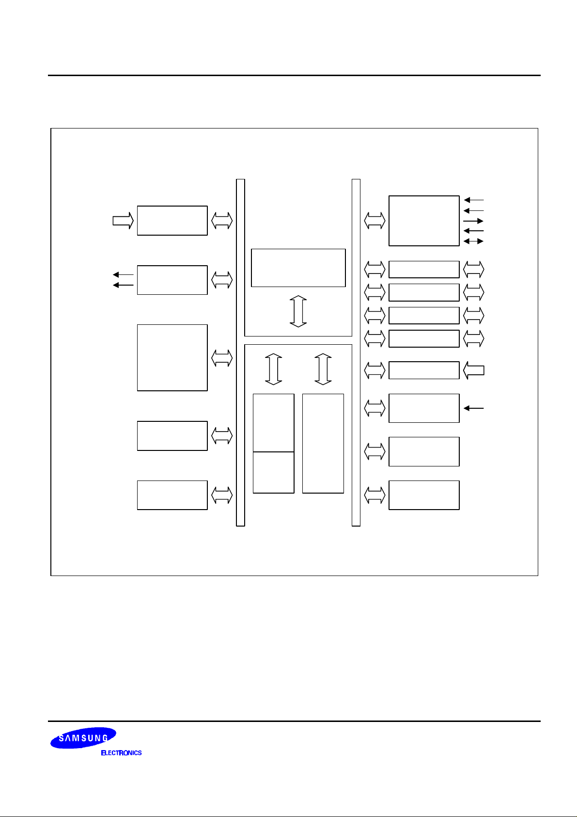
BLOCK DIAGRAM
VDD, VSS
X
IN
XOUT
RESET
LPF
ADC0-ADC4
4-Bit
ADC
System
Control & PLL
PWM0
PWM1
14-Bit
PWM
OSD & CCD
16-Bit
Timer/Counter 2
Watchdog
Timer
ARM7TDMI
16-Bit RISC CPU Core
RAM
3008
Byte
OSD/CCD
RAM
1088 byte
ROM
128 Kbyte
Port0
Port1
Port2
Port3
Ext. Interrupt
Remocon
Receive
16-Bit
Timer/Counter 0
16-Bit
Timer/Counter 1
P0.0-P0.7
P1.0-P1.7
P2.0-P2.7
P3.0
INT0-INT3
IRIN
Figure 1-1. S3C380D Block Diagram
1-3

PRODUCT OVERVIEW S3C380D/F380D
PIN ASSIGNMENTS
P0.0/PWM0
P0.1/PWM1
P0.2
P1.0
P1.1
P1.2
P1.3
P1.4/ADC1
P1.5/ADC2
P1.6/ADC3
P1.7/ADC4
VDD1
VSS1
P2.0/INT0
P2.1/INT1
P2.2/INT2
P2.3/INT3
P2.4
P2.5
P2.6
P2.7/OSDHT
1
2
3
4
5
6
7
8
9
10
11
12
13
14
15
16
17
18
19
20
21
S3C380D
(42-SDIP-600)
42
41
40
39
38
37
36
35
34
33
32
31
30
29
28
27
26
25
24
23
22
P0.3
P0.4
P0.5
P0.6
P0.7
VSS2
VPP
P3.0
VDD2
VSS
XOUT
VSS
VSS3
LPF
CVI IN (ADC0)
V-Sync
H-Sync
Vblank
Vred
Vgreen
Vblue
1-4
Figure 1-2. S3C380D Pin Assignments (42-SDIP)

S3C380D/F380D PRODUCT OVERVIEW
PIN DESCRIPTIONS
Table 1-1. S3C380D Pin Descriptions
Pin Name Pin
Type
P0.0 I/O Input mode or push-pull output mode is
software configurable.
P0.0: PWM0 (14-bit PWM Output)
P0.1-P0.2
P0.3
P0.4-P0.7 General I/O Port (4-bit), Input or Output
P1.0-P1.3 I/O Input/output mode or push-pull output mode
P1.4-P1.7 General I/O Port (4-bit), configurable for
P2.0-P2.3 I/O General I/O Port (4-bit), input or push-pull
P2.4-P2.7 I/O Input mode or push-pull output mode is
P3.0 I/O Input mode or push-pull output mode is
PWM0 O Output pin for 14-bit PWM0 circuit 6 1 P0.0
PWM1 O Output pin for 14-bit PWM1 circuit 3 2 P0.1
ADC1-4 I Input for 4-bit resolution flash A/D
INT0-INT3 I External interrupt input pins 2 14-17 P2.0-3
OSDHT O Halftone control signal output for OSD 6 21 P2.7
IRIN I
General I/O Port (3-bit), Input or n-channel
open-drain output is software configurable.
Pins can withstand up to 6-volt loads. An
alternative function is supported.
P0.1: PWM1 (14-Bit PWM Output)
mode (push-pull or n-channel open drain) is
software configurable.
is software configurable.
digital input or n-channel open drain output.
P1.4-P1.7 can withstand up to 5-volt loads.
Multiplexed for alternative use as external
inputs ADC1-ADC4.
output mode is software configurable.
Multiplexed for alternative use as external
interrupt inputs INT0-INT3.
software configurable. An alternative
function is supported. P2.7: OSDHT
(Halftone signal output)
software configurable.
Converter
Remocon signal input
Normal mode: Remocon signal input
OTP Write mode: VPP=12.5 V
Pin Description Circuit
Type
6 1 PWM0
3 2-3
7 38-41
6 4-7
4 8-11 ADC1-
2 14-17 INT0-INT3
6 18-21 OSDHT
6 35
4 8-11 P1.4-7
1 36 –
Pin
Numbers
42
Share
Pins
PWM1
ADC4
CVI IN I Video signal input 8 28 ADC0
1-5
PRODUCT OVERVIEW S3C380D/F380D
Table 1-1. S3C380D Pin Descriptions (Continued)
Pin Name Pin
RESET
Type
I System reset input pin 9 33 –
Pin Description Circuit
Type
Pin
Numbers
Share
Pins
LPF – PLL filter pin – 29 –
H-SYNC I H-sync input for OSD and CCD 1 26 –
V-SYNC I V-sync input for OSD and CCD 1 27 –
V
blank
V
red
V
green
V
blue
ADC0 I Input for 4-bit resolution flash
O Video blank signal output for OSD and CCD 5 25 –
O Red signal output for OSD and CCD 5 24 –
O Green signal output for OSD and CCD 5 23 –
O Blue signal output for OSD and CCD 5 22 –
8 28 CVI IN
A/D Converter (1.5V-2.0V)
V
DD1
V
SS1
V
SS3
XIN, X
, V
, V
DD2
SS2
OUT
– Power supply pins – 12, 34
13, 37
30
I, O System clock pins (32,768 Hz) – 31,32 –
–
1-6

S3C380D/F380D PRODUCT OVERVIEW
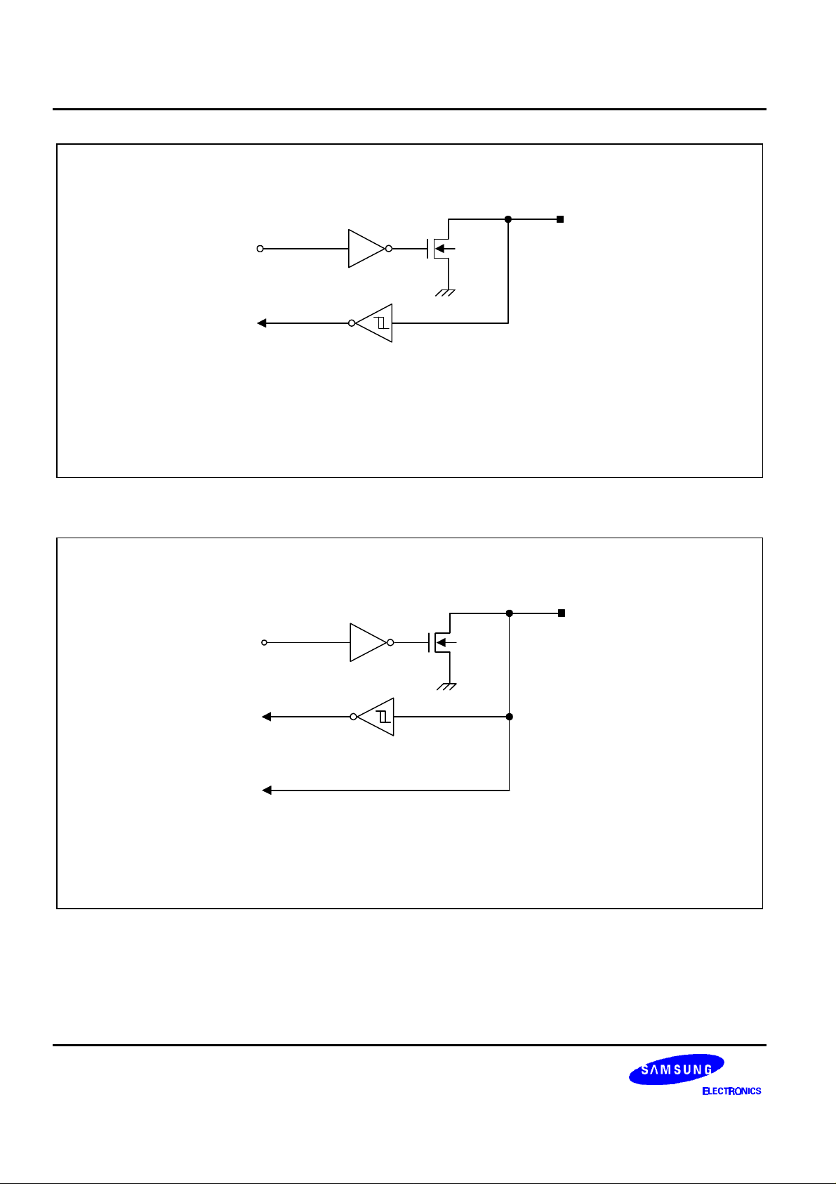
PIN CIRCUITS
In
Schmitt Trigger Input
Noise Filter
Figure 1-3. Pin Circuit Type 1 (H-Sync, V-Sync, IRIN)
VDD
Data
Output
DIsable
Input
Schmitt
Trigger Input
In/Out
INT
Noise Filter
Figure 1-4. Pin Circuit Type 2 (P2.0-P2.3, INT0-INT3)
1-7
PRODUCT OVERVIEW S3C380D/F380D
In/Out
Data
Input
Schmitt Trigger Input
NOTE: Circuit type 3 can withstand up to 6 V loads.
Figure 1-5. Pin Circuit Type 3 (P0.1-P0.3, PWM1)
Data
Input
Schmitt Trigger Input
A/D IN
NOTE: Circuit type 4 can withstand up to 5 V loads.
Figure 1-6. Pin Circuit Type 4 (P1.4-P1.7, ADC1-ADC4)
In/Out
1-8
 Loading...