

Page 1

2003.10.15
现货库存、技术资料、百科信息、热点资讯,精彩尽在鼎好!
S3C2440X RISC MICROPROCESSOR PRODUCT OVERVIEW
PRODUCT OVERVIEW
INTRODUCTION
This manual describes SAMSUNG's S3C2440X 16/32-bit RISC microprocessor. SAMSUNG’s S3C24440X is
designed to provide hand-held devices and general applications with low-power, and high-performance microcontroller solution in small die size. To reduce total system cost, the S3C2440X includes the following components
separate 16KB Instruction and 16KB Data Cache, MMU to handle virtual memory management, LCD Controller
(STN & TFT), NAND Flash Boot Loader, System Manager (chip select logic and SDRAM Controller), 3-ch UART,
4-ch DMA, 4-ch Timers with PWM, I/O Ports, RTC, 8-ch 10-bit ADC and Touch Screen Interface, Camera
interface, IIC-BUS Interface, IIS-BUS Interface, USB Host, USB Device, SD Host & Multi-Media Card Interface, 2ch SPI and PLL for clock generation.
The S3C2440X has been developed using an ARM920T core, 0.13um CMOS standard cells and a memory
complier. Its low-power, simple, elegant and fully static design is particularly suitable for cost- and power-sensitive
applications. It adopts a new bus architecture known as Advanced Micro controller Bus Architecture (AMBA).
The S3C2440X offers outstanding features with its CPU core, a 16/32-bit ARM920T RISC processor designed by
Advanced RISC Machines, Ltd. The ARM920T implements MMU, AMBA BUS, and Harvard cache architecture
with separate 16KB instruction and 16KB data caches, each with an 8-word line length.
By providing a complete set of common system peripherals, the S3C2440X minimizes overall system costs and
eliminates the need to configure additional components. The integrated on-chip functions that are described in this
document include:
• 1.2V internal, 1.8V/2.5V/3.3V memory, 3.3V external I/O microprocessor with 16KB I-Cache/16KB D-
Cache/MMU
• External memory controller (SDRAM Control and Chip Select logic)
• LCD controller (up to 4K color STN and 256K color TFT) with 1-ch LCD-dedicated DMA
• 4-ch DMAs with external request pins
• 3-ch UART (IrDA1.0, 64-Byte Tx FIFO, and 64-Byte Rx FIFO) / 2-ch SPI
• 1-ch multi-master IIC-BUS/1-ch IIS-BUS controller
• SD Host interface version 1.0 & Multi-Media Card Protocol version 2.11 compatible
• 2-port USB Host /1- port USB Device (ver 1.1)
• 4-ch PWM timers & 1-ch internal timer
• WatchDog Timer
• 130-bit general purpose I/O ports / 24-ch external interrupt source
• Power control: Normal, Slow, Idle and Sleep mode
• 8-ch 10-bit ADC and Touch screen interface
• RTC with calendar function
• On-chip clock generator with PLL
Preliminary product information describes products that are in development,
for which full characterization data and associated errata are not yet available
Specifications and information herein are subject to change without notice.
1-1
Page 2

2003.10.15
PRODUCT OVERVIEW S3C2440X
FEATURES
Architecture
• Integrated system for hand-held devices and
general embedded applications.
• 16/32-Bit RISC architecture and powerful
instruction set with ARM920T CPU core.
• Enhanced ARM architecture MMU to support
WinCE, EPOC 32 and Linux.
• Instruction cache, data cache, write buffer and
Physical address TAG RAM to reduce the effect
of main memory bandwidth and latency on
performance.
• ARM920T CPU core supports the ARM debug
architecture.
• Internal Advanced Microcontroller Bus
Architecture (AMBA) (AMBA2.0, AHB/APB).
System Manager
• Little/Big Endian support.
• Address space: 128M bytes for each bank (total
1G bytes).
• Supports programmable 8/16/32-bit data bus
width for each bank.
• Fixed bank start address from bank 0 to bank 6.
• Programmable bank start address and bank size
for bank 7.
• Eight memory banks:
– Six memory banks for ROM, SRAM, and others.
– Two memory banks for ROM/SRAM/
Synchronous DRAM.
• Complete Programmable access cycles for all
memory banks.
• Supports external wait signals to expend the bus
cycle.
• Supports self-refresh mode in SDRAM for power-
down.
NAND Flash Boot Loader
• Supports booting from NAND flash memory.
• 4KB internal buffer for booting.
• Supports storage memory for NAND flash
memory after booting.
• Supports Advanced NAND flash
Cache Memory
• 64-way set-associative cache with I-Cache
(16KB) and D-Cache (16KB).
• 8words length per line with one valid bit and two
dirty bits per line.
• Pseudo random or round robin replacement
algorithm.
• Write-through or write-back cache operation to
update the main memory.
• The write buffer can hold 16 words of data and
four addresses.
Clock & Power Manager
• On-chip MPLL and UPLL:
UPLL generates the clock to operate USB
Host/Device.
MPLL generates the clock to operate MCU at
maximum 400Mhz@ 1.2V.
• Clock can be fed selectively to each function
block by software.
• Power mode: Normal, Slow, Idle, and Sleep
mode
Normal mode: Normal operating mode
Slow mode: Low frequency clock without PLL
Idle mode: The clock for only CPU is stopped.
Sleep mode: The Core power including all
peripherals is shut down.
• Woken up by EINT[15:0] or RTC alarm interrupt
from Sleep mode
• Supports various types of ROM for booting
(NOR/NAND Flash, EEPROM, and others).
1-2
Preliminary product information describes products that are in development,
for which full characterization data and associated errata are not yet available
Specifications and information herein are subject to change without notice.
Page 3

2003.10.15
S3C2440X PRODUCT OVERVIEW
FEATURES (Continued)
Interrupt Controller
• 59 Interrupt sources
(One Watch dog timer, 5 timers, 9 UARTs, 24
external interrupts, 4 DMA, 2 RTC, 2 ADC, 1 IIC,
2SPI,1SDI,2USB,1LCD, 1BatteryFault,1
NAND and 2 Camera)
• Level/Edge mode on external interrupt source
• Programmable polarity of edge and level
• Supports Fast Interrupt request (FIQ) for very
urgent interrupt request
Timer with Pulse Width Modulation (PWM)
• 4-ch 16-bit Timer with PWM / 1-ch 16-bit internal
timer with DMA-based or interrupt-based
operation
• Programmable duty cycle, frequency, and polarity
• Dead-zone generation
• Supports external clock sources
RTC (Real Time Clock)
• Full clock feature: msec, second, minute, hour,
date, day, month, and year
• 32.768 KHz operation
• Alarm interrupt
• Time tick interrupt
General Purpose Input/Output Ports
64-byte Rx FIFO.
DMA Controller
• 4-ch DMA controller
• Supports memory to memory, IO to memory,
memory to IO, and IO to IO transfers
• Burst transfer mode to enhance the transfer rate
A/D Converter & Touch Screen Interface
• 8-ch multiplexed ADC
• Max. 500KSPS and 10-bit Resolution
• Internal FET for direct Touch screen interface
LCD Controller STN LCD Displays Feature
• Supports 3 types of STN LCD panels: 4-bit dual
scan, 4-bit single scan, 8-bit single scan display
type
• Supports monochrome mode, 4 gray levels, 16
gray levels, 256 colors and 4096 colors for STN
LCD
• Supports multiple screen size
– Maximum screen size: 2048x1024
– Recommended screen size: max 800x600
– Maximum virtual screen size is 4 Mbytes.
– Maximum virtual screen size in 256 color mode:
4096x1024, 2048x2048, 1024x4096 and others
• 24 external interrupt ports
• Multiplexed input/output ports
UART
• 3-channel UART with DMA-based or interrupt-
based operation
• Supports 5-bit, 6-bit, 7-bit, or 8-bit serial data
transmit/receive (Tx/Rx)
• Supports external clocks for the UART operation
(UARTCLK)
• Programmable baud rate
• Supports IrDA 1.0
• Loopback mode for testing
• Each channel has internal 64-byte Tx FIFO and
Preliminary product information describes products that are in development,
for which full characterization data and associated errata are not yet available
Specifications and information herein are subject to change without notice.
TFT(Thin Film Transistor) Color Displays Feature
• Supports 1, 2, 4 or 8 bpp (bit-per-pixel) palette
color displays for color TFT
• Supports 16 bpp non-palette true-color displays
for color TFT
• Supports maximum 16M color TFT at 24 bpp
mode
• Supports multiple screen size
– Maximum screen size: 2048x1024
– Recommended screen size: max 800x600
– Maximum virtual screen size is 4Mbytes.
– Maximum virtual screen size in 64K color mode:
2048x1024, and others
1-3
Page 4

2003.10.15
PRODUCT OVERVIEW S3C2440X
FEATURES (Continued)
Watchdog Timer
• 16-bit Watchdog Timer
• Interrupt request or system reset at time-out
IIC-Bus Interface
• 1-ch Multi-Master IIC-Bus
• Serial, 8-bit oriented and bi-directional data
transferscanbemadeatupto100Kbit/sin
Standard mode or up to 400 Kbit/s in Fast mode.
IIS-Bus Interface
• 1-ch IIS-bus for audio interface with DMA-based
operation
• Serial, 8-/16-bit per channel data transfers
• 128 Bytes (64-Byte + 64-Byte) FIFO for Tx/Rx
• Supports IIS format and MSB-justified data format
USB Host
• 2-port USB Host
• Complies with OHCI Rev. 1.0
• Compatible with USB Specification version 1.1
• Compatible with SDIO Card Protocol version 1.0
• Bytes FIFO for Tx/Rx
• DMA based or Interrupt based operation
• Compatible with Multimedia Card Protocol version
2.11
SPI Interface
• Compatible with 2-ch Serial Peripheral Interface
Protocol version 2.11
• 2x8 bits Shift register for Tx/Rx
• DMA-based or interrupt-based operation
Camera Interface
• ITU601/ITU656-format input support (8-bit)
• YCrCb 4:2:2 to 4:2:0 down-sampling
• Up to 1016 Horizontal resolution support
Operating Voltage Range
• Core: 1.2V
• Memory :1.8V/ 2.5V/3.3V
• I/O : 3.3V
USB Device
• 1-port USB Device
• 5 Endpoints for USB Device
• Compatible with USB Specification version 1.1
SD Host Interface
• Compatible with SD Memory Card Protocol
version 1.0
Operating Frequency
• Up to 400MHz
Package
• 289-FBGA
1-4
Preliminary product information describes products that are in development,
for which full characterization data and associated errata are not yet available
Specifications and information herein are subject to change without notice.
Page 5
2003.10.15
S3C2440X PRODUCT OVERVIEW
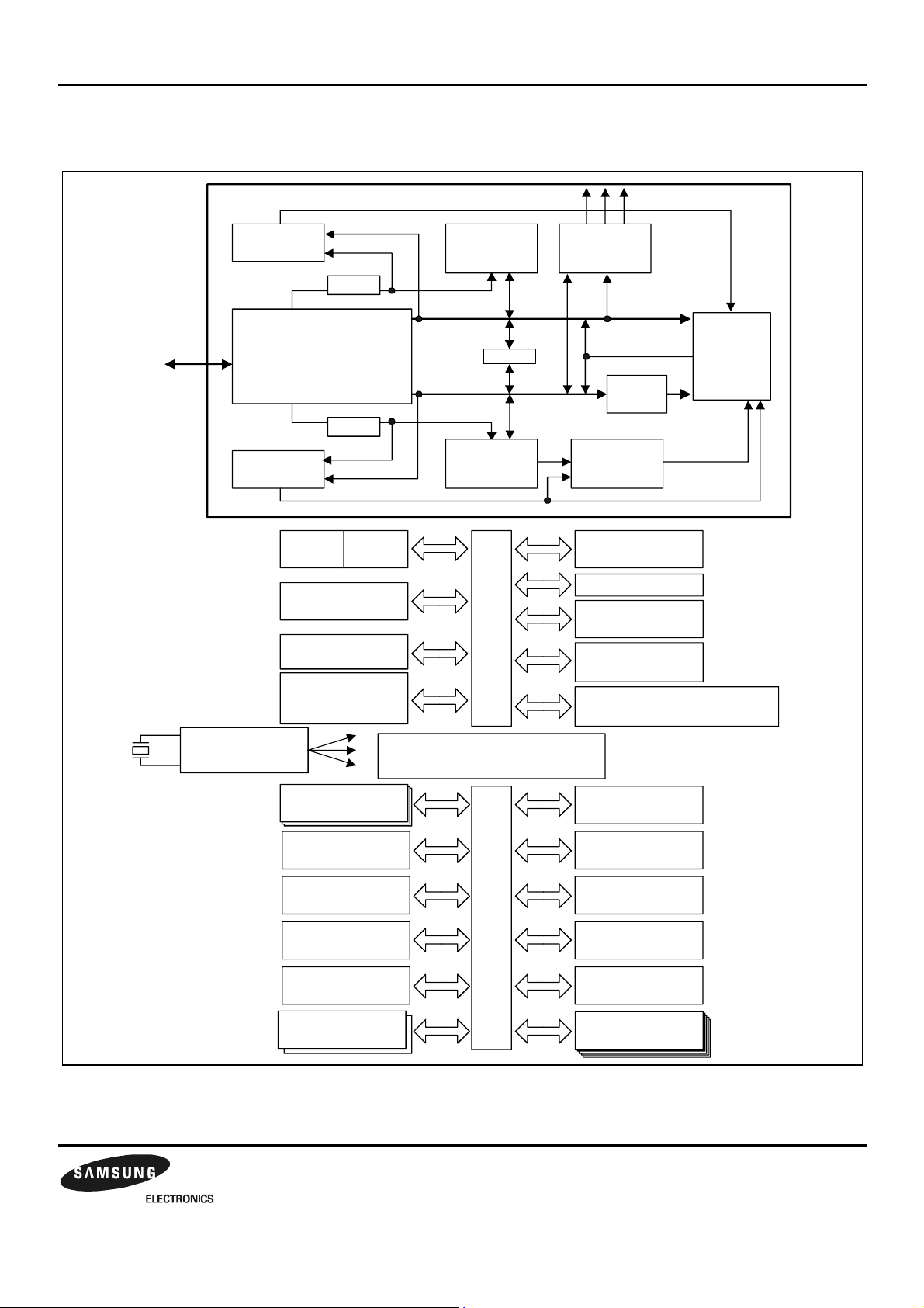
BLOCK DIAGRAM
JTAG
ARM920T
Instruction
MMU
2
A[31:0]
IV
ARM9TDMI
Processor core
(Internal Embedded ICE)
Data
MMU
LCD
CONT.
USB Host CONT.
ExtMaster
NAND Ctrl.
NAND Flash Boot
Loader
C13
C13
IPA[31:0]
DPA[31:0]
LCD
DMA
Instruction
ID[31:0]
DD[31:0]
DVA[31:0]DV2A[31:0]
CACHE
(16KB)
CP15
Data
CACHE
(16KB)
A
H
B
B
U
S
External
Coproc
Interface
Write
Buffer
WriteBack
PA Tag
RAM
BUS CONT.
Arbitor/Decode
Interrupt CONT.
Power
Management
Camera
Interface
Memory CONT.
SRAM/NOR/SDRAM
AMBA
Bus
I/F
WBPA[31:0]
Clock Generator
(MPLL)
Bridge & DMA (4Ch)
UART 0, 1, 2
USB Device
A
P
SDI/MMC
Watchdog
Timer
BUS CONT.
Arbitor/Decode
SPI0,1
SPI
Figure 1-1. S3C2440X Block Diagram
B
B
U
S
I2C
I2S
GPIO
RTC
ADC
Timer/PWM
0 ~ 3, 4(Internal)
Preliminary product information describes products that are in development,
for which full characterization data and associated errata are not yet available
Specifications and information herein are subject to change without notice.
1-5
Page 6
2003.10.15
PRODUCT OVERVIEW S3C2440X
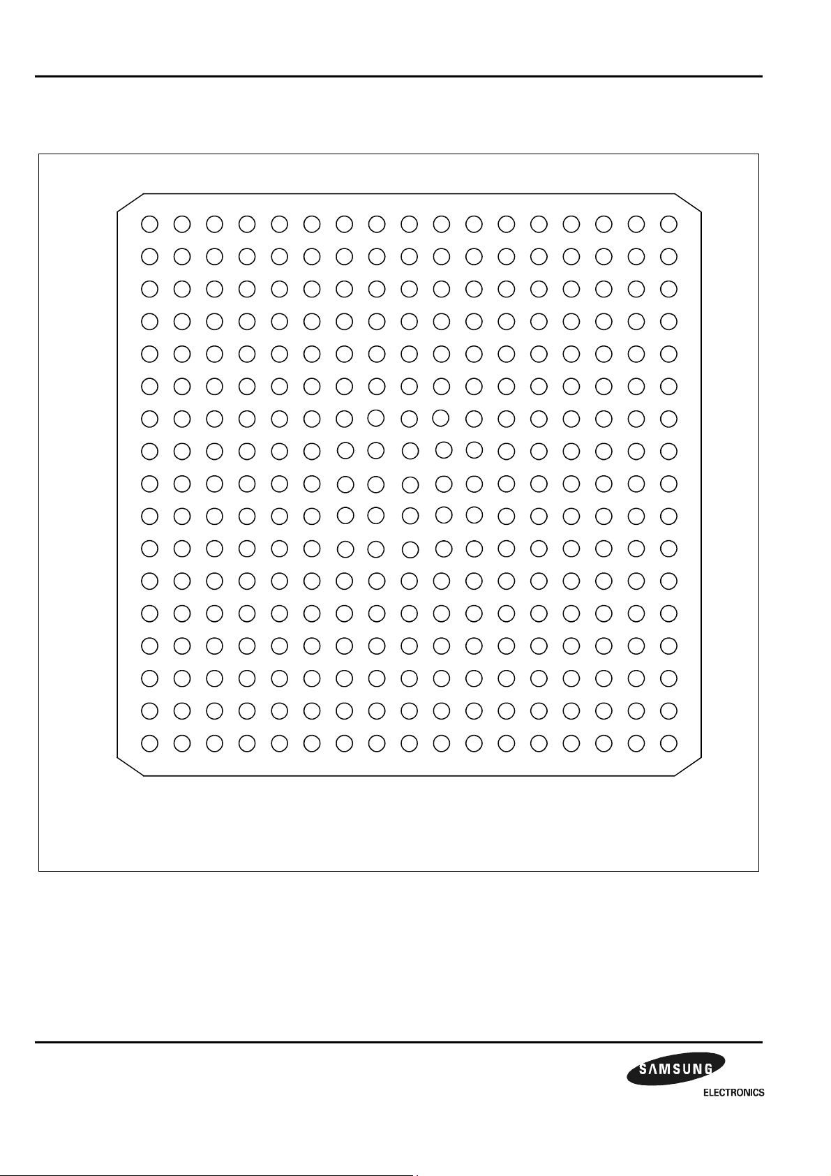
PIN ASSIGNMENTS
U
T
R
P
N
M
L
K
J
H
G
F
E
D
C
B
A
1234567891011121314151617
1-6
BOTTOM VIEW
Figure 1-2. S3C2440X Pin Assignments (289-FBGA)
Preliminary product information describes products that are in development,
for which full characterization data and associated errata are not yet available
Specifications and information herein are subject to change without notice.
Page 7
2003.10.15
S3C2440X PRODUCT OVERVIEW
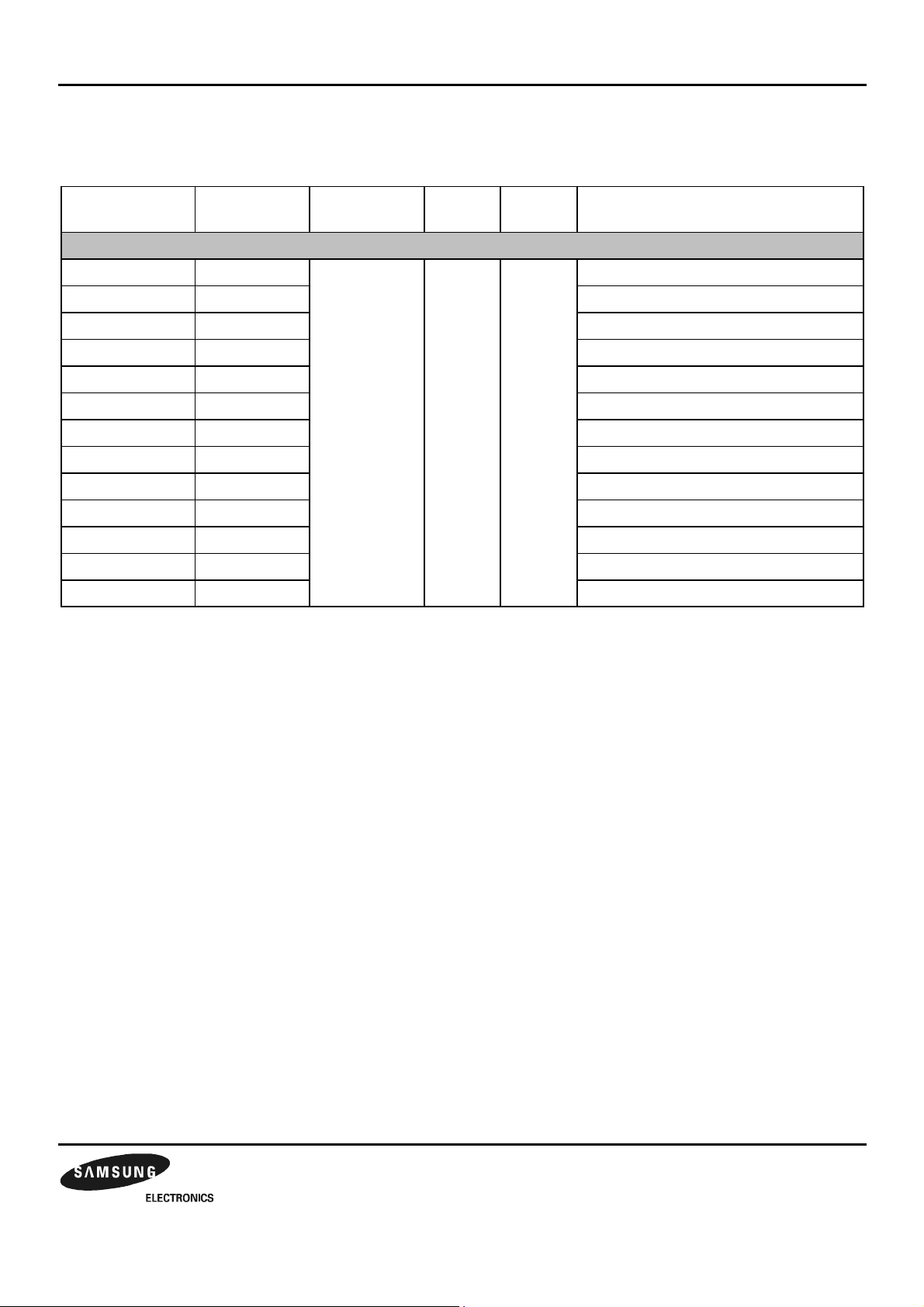
Table 1-1. 289-Pin FBGA Pin Assignments – Pin Number Order (Sheet 1 of 3)
Pin
Number
Pin Name Pin
Number
Pin Name Pin
Number
Pin Name
A1 VDDi C1 VDDMOP E1 nFRE/GPA20
A2 SCKE C2 nGCS5/GPA16 E2 VSSMOP
A3 VSSi C3 nGCS2/GPA13 E3 nGCS7
A4 VSSi C4 nGCS3/GPA14 E4 nWAIT
A5 VSSMOP C5 nOE E5 nBE3
A6 VDDi C6 nSRAS E6 nWE
A7 VSSMOP C7 ADDR4 E7 ADDR1
A8 ADDR10 C8 ADDR11 E8 ADDR6
A9 VDDMOP C9 ADDR15 E9 ADDR14
A10 VDDi C10 ADDR21/GPA6 E10 ADDR23/GPA8
A11 VSSMOP C11 ADDR24/GPA9 E11 DATA2
A12 VSSi C12 DATA1 E12 DATA20
A13 DATA3 C13 DATA6 E13 DATA19
A14 DATA7 C14 DATA11 E14 DATA18
A15 VSSMOP C15 DATA13 E15 DATA17
A16 VDDi C16 DATA16 E16 DATA21
A17 DATA10 C17 VSSi E17 DATA24
B1 VSSMOP D1 ALE/GPA18 F1 VDDi
B2 nGCS1/GPA12 D2 nGCS6 F2 VSSi
B3 SCLK1 D3 nGCS4/GPA15 F3 nFWE/GPA19
B4 SCLK0 D4 nBE0 F4 nFCE/GPA22
B5 nBE1 D5 nBE2 F5 CLE/GPA17
B6 VDDMOP D6 nSCAS F6 nGCS0
B7 ADDR2 D7 ADDR7 F7 ADDR0/GPA0
B8 ADDR9 D8 ADDR5 F8 ADDR3
B9 ADDR12 D9 ADDR16/GPA1 F9 ADDR18/GPA3
B10 VSSi D10 ADDR20/GPA5 F10 DATA4
B11 VDDi D11 ADDR26/GPA11 F11 DATA5
B12 VDDMOP D12 DATA0 F12 DATA27
B13 VSSMOP D13 DATA8 F13 DATA31
B14 VDDMOP D14 DATA14 F14 DATA26
B15 DATA9 D15 DATA12 F15 DATA22
B16 VDDMOP D16 VSSMOP F16 VDDi
B17 DATA15 D17 VSSMOP F17 VDDMOP
Preliminary product information describes products that are in development,
for which full characterization data and associated errata are not yet available
Specifications and information herein are subject to change without notice.
1-7
Page 8
2003.10.15
PRODUCT OVERVIEW S3C2440X
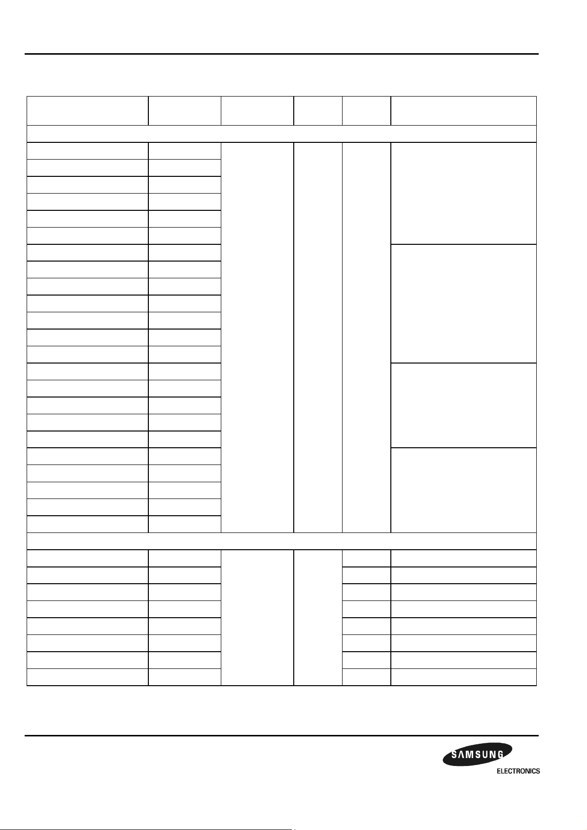
Table 1-1. 289-Pin FBGA Pin Assignments – Pin Number Order (Sheet 2 of 3)
Pin
Number
Pin Name Pin
Number
Pin Name Pin
Number
Pin Name
G1 VSSOP J1 VDDOP L1 LEND/GPC0
G2 CAMHREF/GPJ10 J2 VDDiarm L2 VDDiarm
G3 CAMDATA1/GPJ1 J3 CAMCLKOUT/GPJ11 L3 nXDACK0/GPB9
G4 VDDalive J4 CAMRESET/GPJ12 L4 VCLK/GPC1
G5 CAMPCLK/GPJ8 J5 TOUT1/GPB1 L5 nXBREQ/GPB6
G6 FRnB J6 TOUT0/GPB0 L6 VD1/GPC9
G7 CAMVSYNC/GPJ9 J7 TOUT2/GPB2 L7 VFRAME/GPC3
G8 ADDR8 J8 CAMDATA6/GPJ6 L8 I2SSDI/nSS0/GPE3
G9 ADDR17/GPA2 J9 SDDAT3/GPE10 L9 SPICLK0/GPE13
G10 ADDR25/GPA10 J10 EINT10/nSS0/GPG2 L10 EINT15/SPICLK1/GPG7
G11 DATA28 J11 TXD2/nRTS1/GPH6 L11 EINT22/GPG14
G12 DATA25 J12 PWREN L12 Xtortc
G13 DATA23 J13 TCK L13 EINT2/GPF2
G14 XTIpll J14 TMS L14 EINT5/GPF5
G15 XTOpll J15 RXD2/nCTS1/GPH7 L15 EINT6/GPF6
G16 DATA29 J16 TDO L16 EINT7/GPF7
G17 VSSi J17 VDDalive L17 nRTS0/GPH1
H1 VSSiarm K1 VSSiarm M1 VLINE/GPC2
H2 CAMDATA7/GPJ7 K2 nXBACK/GPB5 M2 LCD_LPCREV/GPC6
H3 CAMDATA4/GPJ4 K3 TOUT3/GPB3 M3 LCD_LPCOE/GPC5
H4 CAMDATA3/GPJ3 K4 TCLK0/GPB4 M4 VM/GPC4
H5 CAMDATA2/GPJ2 K5 nXDREQ1/GPB8 M5 VD9/GPD1
H6 CAMDATA0/GPJ0 K6 nXDREQ0/GPB10 M6 VD6/GPC14
H7 CAMDATA5/GPJ5 K7 nXDACK1/GPB7 M7 VD16/SPIMISO1/GPD8
H8 ADDR13 K8 SDCMD/GPE6 M8 SDDAT1/GPE8
H9 ADDR19/GPA4 K9 SPIMISO0/GPE11 M9 IICSDA/GPE15
H10 ADDR22/GPA7 K10 EINT13/SPIMISO1/GPG5 M10 EINT20/GPG12
H11 VSSOP1 K11 nCTS0/GPH0 M11 EINT17/nRTS1/GPG9
H12 EXTCLK K12 VDDOP M12 VSSA_UPLL
H13 DATA30 K13 TXD0/GPH2 M13 VDDA_UPLL
H14 nBATT_FLT K14 RXD0/GPH3 M14 Xtirtc
H15 nTRST K15 UARTCLK/GPH8 M15 EINT3/GPF3
H16 nRESET K16 TXD1/GPH4 M16 EINT1/GPF1
H17 TDI K17 RXD1/GPH5 M17 EINT4/GPF4
1-8
Preliminary product information describes products that are in development,
for which full characterization data and associated errata are not yet available
Specifications and information herein are subject to change without notice.
Page 9
2003.10.15
S3C2440X PRODUCT OVERVIEW
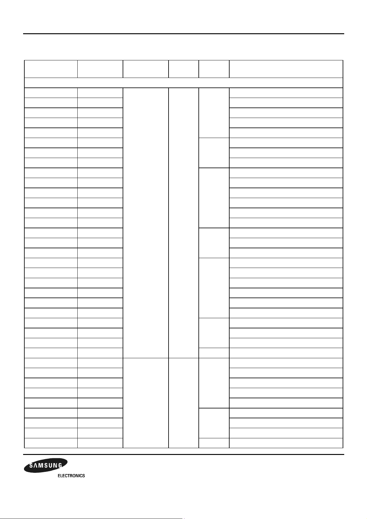
Table 1-1. 289-Pin FBGA Pin Assignments – Pin Number Order (Sheet 3 of 3)
Pin
Number
Pin Name Pin
Number
Pin Name Pin
Number
Pin Name
N1 VSSOP R1 VD3/GPC11 U1 VDDiarm
N2 VD0/GPC8 R2 VD8/GPD0 U2 VDDiarm
N3 VD4/GPC12 R3 VD11/GPD3 U3 VSSOP
N4 VD2/GPC10 R4 VD13/GPD5 U4 VSSiarm
N5 VD10/GPD2 R5 VD18/SPICLK1/GPD10 U5 VD23/nSS0/GPD15
N6 VD15/GPD7 R6 VD21 /GPD13 U6 I2SSDO/I2SSDI/GPE4
N7 VD22/nSS1/GPD14 R7 I2SSCLK/GPE1 U7 VSSiarm
N8 SDCLK/GPE5 R8 SDDAT0/GPE7 U8 IICSCL/GPE14
N9 EINT8/GPG0 R9 CLKOUT0/GPH9 U9 VSSOP
N10 EINT18/nCTS1/GPG10 R10 EINT11/nSS1/GPG3 U10 VSSiarm
N11 DP0 R11 EINT14/SPIMOSI1/GPG6 U11 VDDiarm
N12 DN1/PDN0 R12 NCON U12 EINT19/TCLK1/GPG11
N13 nRSTOUT/GPA21 R13 OM1 U13 EINT23/GPG15
N14 MPLLCAP R14 AIN0 U14 DP1/PDP0
N15 VDD_RTC R15 AIN2 U15 VSSOP
N16 VDDA_MPLL R16 AIN6 U16 Vref
N17 EINT0/GPF0 R17 VSSA_MPLL U17 AIN1
P1 LCD_LPCREVB/GPC7 T1 VSSiarm
P2 VD5/GPC13 T2 VSSiarm
P3 VD7/GPC15 T3 VDDOP
P4 VD12/GPD4 T4 VD17/SPIMOSI1/GPD9
P5 VD14/GPD6 T5 VD19/GPD11
P6 VD20/GPD12 T6 VDDiarm
P7 I2SLRCK/GPE0 T7 CDCLK/GPE2
P8 SDDAT2/GPE9 T8 VDDiarm
P9 SPIMOSI0/GPE12 T9 EINT9/GPG1
P10 CLKOUT1/GPH10 T10 EINT16/GPG8
P11 EINT12/LCD_PWREN T11 EINT21/GPG13
P12 DN0 T12 VDDOP
P13 OM2 T13 OM3
P14 VDDA_ADC T14 VSSA_ADC
P15 AIN3 T15 OM0
P16 AIN7 T16 AIN4
P17 UPLLCAP T17 AIN5
Preliminary product information describes products that are in development,
for which full characterization data and associated errata are not yet available
Specifications and information herein are subject to change without notice.
1-9
Page 10
2003.10.15
PRODUCT OVERVIEW S3C2440X
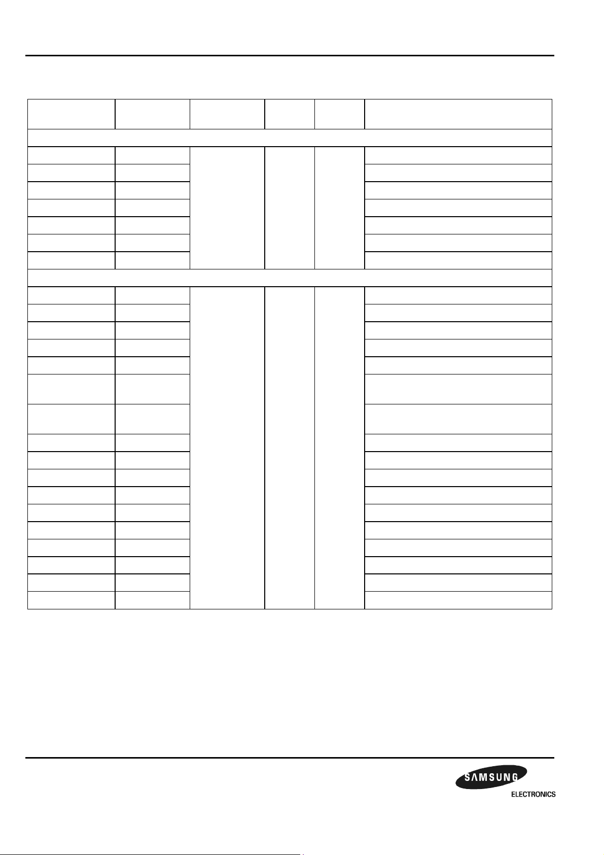
Table 1-2. S3C2440X 289-Pin FBGA Pin Assignments (Sheet 1 of 9)
Pin
Number
Pin
Name
Default
Function
I/O State
@BUS REQ
I/O State
@Sleep
I/O State
@nRESET
F7 ADDR0/GPA0 ADDR0 Hi-z/– O(L)/– O(L) t10s
E7 ADDR1 ADDR1 Hi-z O(L) O(L) t10s
B7 ADDR2 ADDR2 Hi-z O(L) O(L) t10s
F8 ADDR3 ADDR3 Hi-z O(L) O(L) t10s
C7 ADDR4 ADDR4 Hi-z O(L) O(L) t10s
D8 ADDR5 ADDR5 Hi-z O(L) O(L) t10s
E8 ADDR6 ADDR6 Hi-z O(L) O(L) t10s
D7 ADDR7 ADDR7 Hi-z O(L) O(L) t10s
G8 ADDR8 ADDR8 Hi-z O(L) O(L) t10s
B8 ADDR9 ADDR9 Hi-z O(L) O(L) t10s
A8 ADDR10 ADDR10 Hi-z O(L) O(L) t10s
C8 ADDR11 ADDR11 Hi-z O(L) O(L) t10s
B9 ADDR12 ADDR12 Hi-z O(L) O(L) t10s
H8 ADDR13 ADDR13 Hi-z O(L) O(L) t10s
E9 ADDR14 ADDR14 Hi-z O(L) O(L) t10s
I/O Type
C9 ADDR15 ADDR15 Hi-z O(L) O(L) t10s
D9 ADDR16/GPA1 ADDR16 Hi-z/– O(L)/– O(L) t10s
G9 ADDR17/GPA2 ADDR17 Hi-z/– O(L)/– O(L) t10s
F9 ADDR18/GPA3 ADDR18 Hi-z/– O(L)/– O(L) t10s
H9 ADDR19/GPA4 ADDR19 Hi-z/– O(L)/– O(L) t10s
D10 ADDR20/GPA5 ADDR20 Hi-z/– O(L)/– O(L) t10s
C10 ADDR21/GPA6 ADDR21 Hi-z/– O(L)/– O(L) t10s
H10 ADDR22/GPA7 ADDR22 Hi-z/– O(L)/– O(L) t10s
E10 ADDR23/GPA8 ADDR23 Hi-z/– O(L)/– O(L) t10s
C11 ADDR24/GPA9 ADDR24 Hi-z/– O(L)/– O(L) t10s
G10 ADDR25/GPA10 ADDR25 Hi-z/– O(L)/– O(L) t10s
D11 ADDR26/GPA11 ADDR26 Hi-z/– O(L)/– O(L) t10s
R14 AIN0 AIN0 – – AI r10
U17 AIN1 AIN1 – – AI r10
R15 AIN2 AIN2 – – AI r10
P15 AIN3 AIN3 – – AI r10
T16 YM/AIN4 AIN4 –/– –/– AI r10
T17 YP/AIN5 YP –/– –/– AI r10
R16 XM/AIN6 AIN6 –/– –/– AI r10
1-10
Preliminary product information describes products that are in development,
for which full characterization data and associated errata are not yet available
Specifications and information herein are subject to change without notice.
Page 11

2003.10.15
S3C2440X PRODUCT OVERVIEW
Table 1-2. S3C2440X 289-Pin FBGA Pin Assignments (Sheet 2 of 9)
Pin
Number
Pin
Name
Default
Function
I/O State
@BUS REQ
I/O State
@Sleep
I/O State
@nRESET
I/O Type
P16 XP/AIN7 XP –/– –/– AI r10
H6 CAMDATA0/GPJ0 G PJ0 –/– Hi-z/– I t8
G3 CAMDATA1/GPJ1 GPJ1 –/– Hi-z/– I t8
H5 CAMDATA2/GPJ2 G PJ2 –/– Hi-z/– I t8
H4 CAMDATA3/GPJ3 G PJ3 –/– Hi-z/– I t8
H3 CAMDATA4/GPJ4 G PJ4 –/– Hi-z/– I t8
H7 CAMDATA5/GPJ5 G PJ5 –/– Hi-z/– I t8
J8 CAMDATA6/GPJ6 GPJ6 –/– Hi-z/– I t8
H2 CAMDATA7/GPJ7 G PJ7 –/– Hi-z/– I t8
G5 CAMPCLK/GPJ8 GPJ8 –/– Hi-z/– I t8
G7 CAMVSYNC/GPJ9 GPJ9 –/– Hi-z/– I t8
G2 CAMHREF/GPJ10 GPJ10 –/– Hi-z/– I t8
J3 CAMPCLKOUT/GPJ11 GPJ11 –/– O(L)/– I t8
J4 CAMRESET/GPJ12 GPJ12 –/– O(L)/– I t8
D12 DATA0 DATA0 Hi-z Hi-z,O(L) I b12s
C12 DATA1 DATA1 Hi-z Hi-z,O(L) I b12s
E11 DATA2 DATA2 Hi-z Hi-z,O(L) I b12s
A13 DATA3 DATA3 Hi-z Hi-z,O(L) I b12s
F10 DATA4 DATA4 Hi-z Hi-z,O(L) I b12s
F11 DATA5 DATA5 Hi-z Hi-z,O(L) I b12s
C13 DATA6 DATA6 Hi-z Hi-z,O(L) I b12s
A14 DATA7 DATA7 Hi-z Hi-z,O(L) I b12s
D13 DATA8 DATA8 Hi-z Hi-z,O(L) I b12s
B15 DATA9 DATA9 Hi-z Hi-z,O(L) I b12s
A17 DATA10 DATA10 Hi-z Hi-z,O(L) I b12s
C14 DATA11 DATA11 Hi-z Hi-z,O(L) I b12s
D15 DATA12 DATA12 Hi-z Hi-z,O(L) I b12s
C15 DATA13 DATA13 Hi-z Hi-z,O(L) I b12s
D14 DATA14 DATA14 Hi-z Hi-z,O(L) I b12s
B17 DATA15 DATA15 Hi-z Hi-z,O(L) I b12s
C16 DATA16 DATA16 Hi-z Hi-z,O(L) I b12s
E15 DATA17 DATA17 Hi-z Hi-z,O(L) I b12s
E14 DATA18 DATA18 Hi-z Hi-z,O(L) I b12s
Preliminary product information describes products that are in development,
for which full characterization data and associated errata are not yet available
Specifications and information herein are subject to change without notice.
1-11
Page 12

2003.10.15
PRODUCT OVERVIEW S3C2440X
Table 1-2. S3C2440X 289-Pin FBGA Pin Assignments (Sheet 3 of 9)
Pin
Number
Pin
Name
Default
Function
I/O State
@BUS REQ
I/O State
@Sleep
I/O State
@nRESET
I/O Type
E13 DATA19 DATA19 Hi-z Hi-z,O(L) I b12s
E12 DATA20 DATA20 Hi-z Hi-z,O(L) I b12s
E16 DATA21 DATA21 Hi-z Hi-z,O(L) I b12s
F15 DATA22 DATA22 Hi-z Hi-z,O(L) I b12s
G13 DATA23 DATA23 Hi-z Hi-z,O(L) I b12s
E17 DATA24 DATA24 Hi-z Hi-z,O(L) I b12s
G12 DATA25 DATA25 Hi-z Hi-z,O(L) I b12s
F14 DATA26 DATA26 Hi-z Hi-z,O(L) I b12s
F12 DATA27 DATA27 Hi-z Hi-z,O(L) I b12s
G11 DATA28 DATA28 Hi-z Hi-z,O(L) I b12s
G16 DATA29 DATA29 Hi-z Hi-z,O(L) I b12s
H13 DATA30 DATA30 Hi-z Hi-z,O(L) I b12s
F13 DATA31 DATA31 Hi-z Hi-z,O(L) I b12s
P12 DN0 DN0 AI us
N11 DP0 DP0 AI us
N12 DN1/PDN0 DN1 –/– AI us
U14 DP1/PDP0 DP1 –/– AI us
N17 EINT0/GPF0 GPF0 –/– Hi-z/– I t8
M16 EINT1/GPF1 GPF1 –/– Hi-z/– I t8
L13 EINT2/GPF2 GPF2 –/– Hi-z/– I t8
M15 EINT3/GPF3 GPF3 –/– Hi-z/– I t8
M17 EINT4/GPF4 GPF4 –/– Hi-z/– I t8
L14 EINT5/GPF5 GPF5 –/– Hi-z/– I t8
L15 EINT6/GPF6 GPF6 –/– Hi-z/– I t8
L16 EINT7/GPF7 GPF7 –/– Hi-z/– I t8
N9 EINT8/GPG0 GPG0 –/– Hi-z/– I t8
T9 EINT9/GPG1 GPG1 –/– Hi-z/– I t8
J10 EINT10/nSS0/GPG2 GPG2 –/–/– Hi-z/Hi-z/– I t8
R10 EINT11/nSS1/GPG3 GPG3 –/–/– Hi-z/Hi-z/– I t8
P11 EINT12/LCD_PWREN/GPG4 GPG4 –/–/– Hi-z/O(L)/– I t8
K10 EINT13/SPIMISO1/GPG5 GPG5 –/–/– Hi-z/Hi-z/– I tt8
R11 EINT14/SPIMOSI1/GPG6 GPG6 –/–/– Hi-z/Hi-z/– I tt8
L10 EINT15/SPICLK1/GPG7 GPG7 –/–/– Hi-z/Hi-z/– I tt8
1-12
Preliminary product information describes products that are in development,
for which full characterization data and associated errata are not yet available
Specifications and information herein are subject to change without notice.
Page 13

2003.10.15
S3C2440X PRODUCT OVERVIEW
Table 1-2. S3C2440X 289-Pin FBGA Pin Assignments (Sheet 4 of 9)
Pin
Number
Pin
Name
Default
Function
I/O State
@BUS REQ
I/O State
@Sleep
I/O State
@nRESET
I/O Type
T10 EINT16/GPG8 GPG8 –/– Hi-z/– I t8
M11 EINT17/nRTS1/GPG9 GPG9 –/–/– Hi-z/O(H)/– I t8
N10 EINT18/nCTS1/GPG10 GPG10 –/–/– Hi-z/Hi-z/– I t8
U12 EINT19/TCLK1/GPG11 GPG11 –/–/– Hi-z/Hi-z/– I t12
M10 EINT20/GPG12 GPG12 –/– Hi-z/– I t12
T11 EINT21/GPG13 GPG13 –/– Hi-z/– I t12
L11 EINT22/GPG14 GPG14 –/– Hi-z/– I t12
U13 EINT23/GPG15 GPG15 –/– Hi-z/– I t12
H12 EXTCLK EXTCLK – – AI is
P17 UPLLCAP UPLLCAP – – AI r50
N14 MPLLCAP MPLLCAP – – AI r50
H14 nBATT_FLT nBATT_FLT – – I is
D4 nBE0 nBE0 Hi-z Hi-z,O(H) O(H) t10s
B5 nBE1 nBE1 Hi-z Hi-z,O(H) O(H) t10s
D5 nBE2 nBE2 Hi-z Hi-z,O(H) O(H) t10s
E5 nBE3 nBE3 Hi-z Hi-z,O(H) O(H) t10s
R12 NCON NCON – – I is
G6 FRnB FRnB – Hi-z,O(L) I d2s
F3 nFWE/GPA19 GPA19 O(H)/– Hi-z,O(H)/– O(H) t10s
E1 nFRE/GPA20 GPA20 O(H)/– Hi-z,O(H)/– O(H) t10s
F4 nFCE/GPA22 GPA21 O(H)/– Hi-z,O(H)/– O(H) t10s
F5 CLE/GPA17 GPA17 O(L)/– Hi-z,O(L)/– O(L) t10s
D1 ALE/GPA18 GPA18 O(L)/– Hi-z,O(L)/– O(L) t10s
N13 nRSTOUT/GPA21 GPA21 –/– O(L)/– O(L) b8
C5 nOE nOE Hi-z Hi-z,O(H) O (H) t10s
H16 nRESET nRESET – – I is
F6 nGCS0 nGCS0 Hi-z Hi-z,O(H) O(H) t10s
B2 nGCS1/GPA12 GPA12 Hi-z/– Hi-z,O(H)/– O(H) t10s
C3 nGCS2/GPA13 GPA13 Hi-z/– Hi-z,O(H)/– O(H) t10s
C4 nGCS3/GPA14 GPA14 Hi-z/– Hi-z,O(H)/– O(H) t10s
D3 nGCS4/GPA15 GPA15 Hi-z/– Hi-z,O(H)/– O(H) t10s
C2 nGCS5/GPA16 GPA16 Hi-z/– Hi-z,O(H)/– O(H) t10s
D2 nGCS6 nGCS6 Hi-z Hi-z,O(H) O(H) t10s
Preliminary product information describes products that are in development,
for which full characterization data and associated errata are not yet available
Specifications and information herein are subject to change without notice.
1-13
Page 14

2003.10.15
PRODUCT OVERVIEW S3C2440X
Table 1-2. S3C2440X 289-Pin FBGA Pin Assignments (Sheet 5 of 9)
Pin
Number
Pin
Name
Default
Function
I/O State
@BUS REQ
I/O State
@Sleep
I/O State
@nRESET
E3 nGCS7 nGCS7 Hi-z Hi-z,O(H) O(H) t10s
D6 nSCAS nSCAS Hi-z Hi-z,O(H) O(H) t10s
C6 nSRAS nSRAS Hi-z Hi-z,O(H) O(H) t10s
H15 nTRST nTRST I – I is
E4 nWAIT nWAIT – Hi-z,O(L) I d2s
E6 nWE nWE Hi-z Hi-z,O(H) O(H) t10s
J6 TOUT0/GPB0 GPB0 –/– O(L)/– I t8
J5 TOUT1/GPB1 GPB1 –/– O(L)/– I t8
J7 TOUT2/GPB2 GPB2 –/– O(L)/– I t8
K3 TOUT 3/GPB3 GPB3 –/– O(L)/– I t8
K4 TCLK0/GPB4 GPB4 –/– –/– I t8
K2 nXBACK/GPB5 GPB5 –/– O(H)/– I t8
L5 nXBREQ/GPB6 GPB6 –/– –/– I t8
K7 nXDACK1/GPB7 GPB7 –/– O(H)/– I t8
K5 nXDREQ1/GPB8 GPB8 –/– –/– I t8
I/O Type
L3 nXDACK0/GPB9 GPB9 –/– O(H)/– I t8
K6 nXDREQ0/GPB10 GPB10 –/– –/– I t8
T15 OM0 OM0 – – I is
R13 OM1 OM1 – – I is
P13 OM2 OM2 – – I is
T13 OM3 OM3 – – I is
J12 PWREN PWRENO(H)O(L)O(H)b8
K11 nCTS0/GPH0 GPH0 –/– –/– I t8
L17 nRTS0/GPH1 GPH1 –/– O(H)/– I t8
K13 TXD0/GPH2 GPH2 –/– O(H)/– I t8
K14 RXD0/GPH3 GPH3 –/– –/– I t8
K16 TXD1/GPH4 GPH4 –/– O(H)/– I t8
K17 RXD1/GPH5 GPH5 –/– –/– I t8
J11 TXD2/nRTS1/GPH6 GPH6 –/–/– O(H)/O(H)/– I t8
J15 RXD2/nCTS1/GPH7 GPH7 –/–/– Hi-z/Hi-z/– I t8
K15 UARTCLK/GPH8 GPH8 –/– Hi-z/– I t8
R9 CLKOUT0/GPH9 GPH9 –/– O(L)/– I t12
P10 CLKOUT1/GPH10 GPH10 –/– O(L)/– I t12
1-14
Preliminary product information describes products that are in development,
for which full characterization data and associated errata are not yet available
Specifications and information herein are subject to change without notice.
Page 15

2003.10.15
S3C2440X PRODUCT OVERVIEW
Table 1-2. S3C2440X 289-Pin FBGA Pin Assignments (Sheet 6 of 9)
Pin
Number
Pin
Name
Default
Function
I/O State
@BUS REQ
I/O State
@Sleep
I/O State
@nRESET
A2 SCKE SCKE Hi-z O(L) O(H) t10s
B4 SCLK0 SCLK0 Hi-z O(L) O(SCLK) t12s
B3 SCLK1 SCLK1 Hi-z O(L) O(SCLK) t12s
P7 I2SLRCK/GPE0 GPE0 –/– Hi-z/– I t8
R7 I2SSCLK/GPE1 GPE1 –/– Hi-z/– I t8
T7 CDCLK/GPE2 GPE2 –/– Hi-z/– I t8
L8 I2SSDI/nSS0/GPE3 GPE3 –/–/– Hi-z/Hi-z/– I t8
U6 I2SSDO/I2SSDI/GPE4 GPE4 –/–/– O(L)/Hi-z/– I t8
N8 SDCLK/GPE5 GPE5 –/– O(L)/– I t8
K8 SDCMD/GPE6 GPE6 –/– Hi-z/– I t8
R8 SDDAT0/GPE7 GPE7 –/– Hi-z/– I t8
M8 SDDAT1/GPE8 GPE8 –/– Hi-z/– I t8
P8 SDDAT2/GPE9 GPE9 –/– Hi-z/– I t8
J9 SDDAT3/GPE10 GPE10 –/– Hi-z/– I t8
K9 SPIMISO0/GPE11 GPE11 –/– Hi-z/– I tt8
I/O Type
P9 SPIMOSI0/GPE12 GPE12 –/– Hi-z/– I tt8
L9 SPICLK0/GPE13 GPE13 –/– Hi-z/– I tt8
U8 IICSCL/GPE14 GPE14 –/– Hi-z/– I d8
M9 IICSDA/GPE15 GPE15 –/– Hi-z/– I d8
J13 TCK TCK I – I is
H17 TDI TDI I – I is
J16 TDO TDO O O O ot
J14 TMS TMS I – I is
L1 LEND/GPC0 GPC0 –/– O(L)/– I t8
L4 VCLK/GPC1 GPC1 –/– O(L)/– I t8
M1 VLINE/GPC2 GPC2 –/– O(L)/– I t8
L7 VFRAME/GPC3 GPC3 –/– O(L)/– I t8
M4 VM/GPC4 GPC4 –/– O(L)/– I t8
M3 LCD_LPCOE/GPC5 GPC5 –/– O(L)/– I t8
M2 LCD_LPCREV/GPC6 GPC6 –/– O(L)/– I t8
P1 LCD_LPCREVB/GPC7 GPC7 –/– O(L)/– I t8
N2 VD0/GPC8 GPC8 –/– O(L)/– I t8
L6 VD1/GPC9 GPC9 –/– O(L)/– I t8
Preliminary product information describes products that are in development,
for which full characterization data and associated errata are not yet available
Specifications and information herein are subject to change without notice.
1-15
Page 16

2003.10.15
PRODUCT OVERVIEW S3C2440X
Table 1-2. S3C2440X 289-Pin FBGA Pin Assignments (Sheet 7 of 9)
Pin
Number
Pin
Name
Default
Function
I/O State
@BUS REQ
I/O State
@Sleep
I/O State
@nRESET
N4 VD2/GPC10 GPC10 –/– O(L)/– I t8
R1 VD3/GPC11 GPC11 –/– O(L)/– I t8
N3 VD4/GPC12 GPC12 –/– O(L)/– I t8
P2 VD5/GPC13 GPC13 –/– O(L)/– I t8
M6 VD6/GPC14 GPC14 –/– O(L)/– I t8
P3 VD7/GPC15 GPC15 –/– O(L)/– I t8
R2 VD8/GPD0 GPD0 –/– O(L)/– I t8
M5 VD9/GPD1 GPD1 –/– O(L)/– I t8
N5 VD10/GPD2 GPD2 –/– O(L)/– I t8
R3 VD11/GPD3 GPD3 –/– O(L)/– I t8
P4 VD12/GPD4 GPD4 –/– O(L)/– I t8
R4 VD13/USBTXDN1/GPD5 GPD5 –/–/– O(L)/O/– I t8
P5 VD14/USBTXDP1/GPD6 GPD6 –/–/– O(L)/O/– I t8
N6 VD15/USBOEN1/GPD7 GPD7 –/–/– O(L)/O/– I t8
M7 VD16/SPIMISO1/GPD8 GPD8 –/–/– O(L)/Hi-z/– I tt8
I/O Type
T4 VD17/SPIMOSI1/GPD9 GPD9 –/–/– O(L)/Hi-z/– I tt8
R5 VD18/SPICLK1/GPD10 GPD10 –/–/– O(L)/Hi-z/– I tt8
T5 VD19/USBRXDP1/GPD11 GPD11 –/–/– O(L)/Hi-z/– I t8
P6 VD20/USBRXDN1/GPD12 G PD12 –/–/– O(L)/Hi-z/– I t8
R6 VD21/USBRXD1/GPD13 GPD13 –/–/– O(L)/Hi-z/– I t8
N7 VD22/nSS1/GPD14 GPD14 –/–/– O(L)/Hi-z/– I t8
U5 VD23/nSS0/GPD15 GPD15 –/–/– O(L)/Hi-z/– I t8
U16 Vref Vref – – AI ia
G14 XTIpll XTIpll – – AI m26
M14 Xtirtc Xtirtc – – AI nc
G15 XTOpll XTOpll – – AO m26
L12 Xtortc Xtortc – – AO nc
N15 VDD_RTC VDD_RTC P P P drtc
P14 VDDA_ADC VDDA_ADC P P P d33t
N16 VDDA_MPLL VDDA_MPLL P P P d33t
M13 VDDA_UPLL VDDA_UPLL P P P d33t
G4 VDDalive VDDalive P P P d12i
J17 VDDalive VDDalive P P P d12i
1-16
Preliminary product information describes products that are in development,
for which full characterization data and associated errata are not yet available
Specifications and information herein are subject to change without notice.
Page 17
2003.10.15
S3C2440X PRODUCT OVERVIEW
Table 1-2. S3C2440X 289-Pin FBGA Pin Assignments (Sheet 8 of 9)
Pin
Number
Pin
Name
Default
Function
I/O State
@BUS REQ
I/O State
@Sleep
I/O State
@nRESET
I/O Type
A1 VDDi VDDi P P P d12c
A10 VDDi VDDi P P P d12c
A16 VDDi VDDi P P P d12c
A6 VDDi VDDi P P P d12c
B11 VDDi VDDi P P P d12c
F1 VDDi VDDi P P P d12c
F16 VDDi VDDi P P P d12c
J2 VDDiarm VDDiarm P P P d12c
L2 VDDiarm VDDiarm P P P d12c
T6 VDDiarm VDDiarm P P P d12c
T8 VDDiarm VDDiarm P P P d12c
U1 VDDiarm VDDiarm P P P d12c
U11 VDDiarm VDDiarm P P P d12c
U2 VDDiarm VDDiarm P P P d12c
A9 VDDMOP VDDMOP P P P d33o
B12 VDDMOP VDDMOP P P P d33o
B14 VDDMOP VDDMOP P P P d33o
B16 VDDMOP VDDMOP P P P d33o
B6 VDDMOP VDDMOP P P P d33o
C1 VDDMOP VDDMOP P P P d33o
F17 VDDMOP VDDMOP P P P d33o
J1 VDDOP VDDOP P P P d33o
T12 VDDOP VDDOP P P P d33o
T3 VDDOP VDDOP P P P d33o
K12 VDDOP VDDOP P P P d33o
T14 VSSA_ADC VSSA_ADC P P P st
R17 VSSA_MPLL VSSA_MPLL P P P st
M12 VSSA_UPLL VSSA_UPLL P P P st
A12 VSSi VSSi P P P si
A3 VSSi VSSi P P P si
A4 VSSi VSSi P P P si
B10 VSSi VSSi P P P si
C17 VSSi VSSi P P P si
Preliminary product information describes products that are in development,
for which full characterization data and associated errata are not yet available
Specifications and information herein are subject to change without notice.
1-17
Page 18
2003.10.15
PRODUCT OVERVIEW S3C2440X
Table 1-2. S3C2440X 289-Pin FBGA Pin Assignments (Sheet 9 of 9)
Pin
Number
Pin
Name
Default
Function
I/O State
@BUS REQ
I/O State
@Sleep
I/O State
@nRESET
F2 VSSi VSSi P P P si
G17 VSSi VSSi P P P si
H1 VSSiarm VSSiarm P P P si
K1 VSSiarm VSSiarm P P P si
T1 VSSiarm VSSiarm P P P si
T2 VSSiarm VSSiarm P P P si
U10 VSSiarm VSSiarm P P P si
U4 VSSiarm VSSiarm P P P si
U7 VSSiarm VSSiarm P P P si
A11 VSSMOP VSSMOP P P P so
A15 VSSMOP VSSMOP P P P so
A5 VSSMOP VSSMOP P P P so
A7 VSSMOP VSSMOP P P P so
B1 VSSMOP VSSMOP P P P so
B13 VSSMOP VSSMOP P P P so
I/O Type
D16 VSSMOP VSSMOP P P P so
D17 VSSMOP VSSMOP P P P so
E2 VSSMOP VSSMOP P P P so
G1 VSSOP VSSOP P P P so
N1 VSSOP VSSOP P P P so
U15 VSSOP VSSOP P P P so
U3 VSSOP VSSOP P P P so
U9 VSSOP VSSOP P P P so
H11 VSSOP VSSOP P P P so
1-18
Preliminary product information describes products that are in development,
for which full characterization data and associated errata are not yet available
Specifications and information herein are subject to change without notice.
Page 19
2003.10.15
S3C2440X PRODUCT OVERVIEW
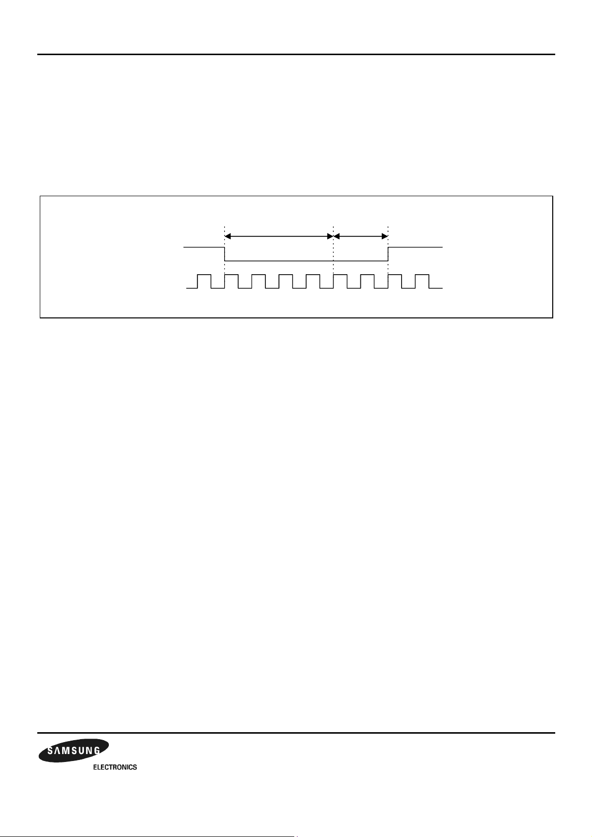
NOTE:
1. The @BUS REQ. shows the pin state at the external bus, which i s used by the other bus master.
2. ' – ‘ mark indicates the unchange d pin state at Bus Request mode.
3. Hi-z or Pre means Hi-z or early state and it is det ermined by th e setting of MISCCR register.
4. AI/AO means analog input/analog output.
5. P, I, and O mean power, input and output respectively.
6. The I/O state @nRESET shows the pin status in the @nRESET duration below.
@nRESET4FCLK
nRESET
FCLK
Preliminary product information describes products that are in development,
for which full characterization data and associated errata are not yet available
Specifications and information herein are subject to change without notice.
1-19
Page 20
2003.10.15
PRODUCT OVERVIEW S3C2440X
7. The t able below shows I/O types and the descriptions.
I/O Type Descriptions
d12i(vdd12ih) 1.2V Vdd for alive power
d12c(vdd12ih_core), si(vssih) 1.2V Vdd/Vss for internal logic
d33o(vdd33oph), so(vssoph) 3.3V Vdd/Vss for external logic
d33t(vdd33th_abb), st(vssbbh_abb) 3.3V Vdd/Vss for analog circuitry
drtc(vdd30th_rtc) 3.0V Vdd for RTC power
t8(phbsu100ct8sm)
Bi-directional pad, LVCMOS schmitt-trigger, 100Kohm pull-up resistor with
control, tri-state, Io=8mA
is(phis) Input pad, LVCMOS schmitt-trigger level
us(pbusb0) USB pad
t10(phtot10cd) 5V tolerant Output pad, Tri-state .
ot(phot8) Output pad, tri-state, Io=8mA
b8(phob8) Output pad, Io=8mA
t16(phot16sm) Output pad, tri-state, medium slew rate, Io=16mA
r10(phiar10_abb) Analog input pad with 10-ohm resistor
ia(phia_abb) Analog input pad
gp(phgpad_option) Pad for analog pin
m26(phsoscm26_2440) Oscillator cell with enable and feedback resistor
tt8(phtbsu100ct8sm)
t12(phbsu100ct12sm)
5V Tolerant Bi-directional pad, LVCMOS schmitt-trigger, 100Kohm pull-up
resistor with control, tri -state, medium slew rate, Io=8mA
Bi-directional pad, LVCMOS schmitt-trigger, 100Kohm pull-up resistor with
control, tri-state, Io=12mA
d2(phtod2) 5v tolerant Output pad , Open Drain , Io=2mA
d8(phbsd8sm) Bi-directional pad, LVCMOS schmitt-trigger, Open Drain, Io=8mA
t10s(phtot10cd_10_2440x)
b12s(phtbsu100ct12cd_12_2440x)
d2s(phtbsd2_2440x)
5V Tolerant output pad, LVCMOS , tri -state, output drive strenth control,
Io=4,6,8,10mA
5V Tolerant Bi-directional pad, LVCMOS schmitt-trigger, 100Kohm pull-up
resistor with control, tri -state,output drive strenth control, Io=6,8,10,12mA
5V Tolerant Bi-directional pad, LVCMOS schmitt-trigger, open-drain, output
drive strenth ignore,
r50(phoar50_abb) Analog Output pad, 50Kohm resistor, Separated bulk-bias
t12s(phtot12cd_12_2440x)
5V Tolerant output pad, LVCMOS , tri -state, output drive strenth control,
Io=6,8,12,16mA
nc(phnc) No connection pad
1-20
Preliminary product information describes products that are in development,
for which full characterization data and associated errata are not yet available
Specifications and information herein are subject to change without notice.
Page 21
2003.10.15
S3C2440X PRODUCT OVERVIEW
SIGNAL DESCRIPTIONS
Table 1-3. S3C2440X Signal Descriptions (Sheet 1 of 6)
Signal I/O Descriptions
Bus Controller
OM[1:0] I OM[1:0] sets S3C2440X in the TEST mode, which is used only at fabrication. Also, it
determines the bus width of nGCS0. The pull-up/down resistor determines the logic
level during RESET cycle.
00:Nand-boot 01:16-bit 10:32-bit 11:Test mode
ADDR[26:0] O ADDR[26:0] (Address Bus) outputs the memory address of the corresponding bank .
DATA[31:0] IO DATA[31:0] (Data Bus) inputs data during memory read and outputs data during
memory write. The bus width is programmable among 8/16/32-bit.
nGCS[7:0] O nGCS[7:0] (General Chip Select) are activated when the address of a memory is
within the address region of each bank. The number of access cycles and the bank
size can be programmed.
nWE O nWE (Write Enable) indicates that the current bus cycle is a write cycle.
nOE O nOE (Output Enable) indicates that the current bus cycle is a read cycle.
nXBREQ I nXBREQ (Bus Hold Request) allows another bus master to request control of the
local bus. BACK active indicates that bus control has been granted.
nXBACK O nXBACK (Bus Hold Acknowledge) indicates that the S3C2440X has surrendered
control of the local bus to another bus master.
nWAIT I nWAIT requests to prolong a current bus cycle. As long as nWAIT is L, the current
bus cycle cannot be completed.
SDRAM/SRAM
nSRAS O SDRAM Row Address Strobe
nSCAS O SDRAM Column Address Strobe
nSCS[1:0] O SDRAM Chip Select
DQM[3:0] O SDRAM Data Mask
SCLK[1:0] O SDRAM Clock
SCKE O SDRAM Clock Enable
nBE[3:0] O Upper Byte/Lower Byte Enable(In case of 16-bit SRAM)
nWBE[3:0] O Write Byte Enable
NAND Flash
CLE O Command Latch Enable
ALE O Address Latch Enable
nFCE O Nand Flash Chip Enable
nFRE O Nand Flash Read Enable
nFWE O Nand Flash W rite Enable
NCON I Nand Flash Configuration
FRnB I Nand Flash Ready/Busy
Preliminary product information describes products that are in development,
for which full characterization data and associated errata are not yet available
Specifications and information herein are subject to change without notice.
* If NAND flash controller isn’t used, it has to be
pull-up. (3.3V)
1-21
Page 22
2003.10.15
PRODUCT OVERVIEW S3C2440X
Table 1-3. S3C2440X Signal Descriptions (Sheet 2 of 6)
Signal I/O Descriptions
LCD Control Unit
VD[23:0] O
LCD_PWREN O
VCLK O
VFRAME O
VLINE O
VM O
VSYNC O
HSYNC O
VDEN O
LEND O
STV O
CPV O
LCD_HCLK O
TP O
STH O
LCD_LPCOE O
LCD_LPCREV O
STN/TFT/SEC TFT: LCD Data Bus
STN/TFT/SEC TFT: LCD panel power enable control signal
STN/TFT: LCD clock signal
STN: LCD Frame signal
STN: LCD line signal
STN: VM alternates the polarity of the row and column voltage
TFT: Vertical synchronous signal
TFT: Horizontal synchronous signal
TFT: Data enable signal
TFT: Line End signal
SEC TFT: SEC(Samsung Electronics Company) TFT LCD panel control signal
SEC TFT: SEC(Samsung Electronics Company) TFT LCD panel control signal
SEC TFT: SEC(Samsung Electronics Company) TFT LCD panel control signal
SEC TFT: SEC(Samsung Electronics Company) TFT LCD panel control signal
SEC TFT: SEC(Samsung Electronics Company) TFT LCD panel control signal
SEC TFT: Timing control signal for specific TFT LCD
SEC TFT: Timing control signal for specific TFT LCD
LCD_LPCREVB O
SEC TFT: Timing control signal for specific TFT LCD
CAMERA Interface
CAMRESET O Software Reset to the Camera
CAMCLKOUT O Master Clock to the Camera
CAMPCLK I Pixel clock from Camera
CAMHREF I Horizontal sync signal from Camera
CAMVSYNC I Vertical sync signal from Camera
CAMDATA[7:0] I Pixel data for YCbCr
Interrupt Control Unit
EINT[23:0] I External Interrupt request
DMA
nXDREQ[1:0] I External DMA request
nXDACK[1:0] O External DMA acknowledge
1-22
Preliminary product information describes products that are in development,
for which full characterization data and associated errata are not yet available
Specifications and information herein are subject to change without notice.
Page 23
2003.10.15
S3C2440X PRODUCT OVERVIEW
Table 1-3. S3C2440X Signal Descriptions (Sheet 3 of 6)
Signal I/O Descriptions
UART
RxD[2:0] I UART receives data input
TxD[2:0] O UART transmits data output
nCTS[1:0] I UART clear to send input signal
nRTS[1:0] O UART request to send output signal
UARTCLK I UART clock signal
ADC
AIN[7:0] AI ADC input[7:0]. If it isn’t used pin, it has to be Low (Ground).
Vref AI ADC Vref
IIC-Bus
IICSDA IO IIC-bus data
IICSCL IO IIC-bus clock
IIS-Bus
I2SLRCK IO IIS-bus channel select clock
I2SSDO O IIS-bus serial data output
I2SSDI I IIS-bus serial data input
I2SSCLK IO IIS-bus serial clock
CDCLK O CODEC system clock
Touch Screen
nXPON O Plus X-axis on-off control signal
XMON O Minus X-axis on-off control signal
nYPON O Plus Y-axis on-off control signal
YMON O Minus Y-axis on-off control signal
USB Host
DN[1:0] IO DATA(–) from USB host
DP[1:0] IO DATA(+) from USB host
USB Device
PDN0 IO DATA(–) for USB peripheral
PDP0 IO DATA(+) for USB peripheral
SPI
SPIMISO[1:0] IO SPIMISO is the master data input line, when SPI is configured as a master.
When SPI is configured as a slave, these pins reverse its role.
SPIMOSI[1:0] IO SPIMOSI is the master data output line, when SPI is configured as a master.
When SPI is configured as a slave, these pins reverse its role.
SPICLK[1:0] IO SPI clock
nSS[1:0] I SPI chip select(only for slave mode)
Preliminary product information describes products that are in development,
for which full characterization data and associated errata are not yet available
Specifications and information herein are subject to change without notice.
1-23
Page 24
2003.10.15
PRODUCT OVERVIEW S3C2440X
Table 1-3. S3C2440X Signal Descriptions (Sheet 4 of 6)
Signal I/O Description
SD
SDDAT[3:0] IO SD receive/transmit data
SDCMD IO SD receive response/ transmit command
SDCLK O SD clock
General Port
GPn[116:0] IO General input/output ports (some ports are output only)
TIMMER/PWM
TOUT[3:0] O Timer output[3:0]
TCLK[1:0] I External timer clock input
JTAG TEST LOGIC
nTRST I nTRST(TAP Controller Reset) resets the TAP controller at start.
If debugger is used, A 10K pull-up resistor has to be connected.
If debugger(black ICE) is not used, nTRST pin must be issued by a low active
pulse(Typically connected to nRESET).
TMS I TMS (TAP Controller Mode Select) controls the sequence of the TAP controller's
states. A 10K pull-up resistor has to be connected to TMS pin.
TCK I TCK (TAP Controller Clock) provides the clock input for the JTAG logic.
A 10K pull-up resistor must be connected to TCK pin.
TDI I TDI (TAP Controller Data Input) is the serial input for test instructions and data.
A 10K pull-up resistor must be connected to TDI pin.
TDO O TDO (TAP Controller Data Output) is the serial output for test instructions and data.
1-24
Preliminary product information describes products that are in development,
for which full characterization data and associated errata are not yet available
Specifications and information herein are subject to change without notice.
Page 25
2003.10.15
S3C2440X PRODUCT OVERVIEW
Table 1-3. S3C2440X Signal Descriptions (Sheet 5 of 6)
Signal I/O Description
Reset, Clock & Power
XTOpll AO Crystal Output for internal osc circuit.
When OM[3:2] = 00b, XTIpll is used for MPLL CLK source and UPLL CLK source.
When OM[3:2] = 01b, XTIpll is used for MPLL CLK source only.
When OM[3:2] = 10b, XTIpll is used for UPLL CLK source only.
If it isn't used, it has to be a floating pin.
MPLLCAP AI Loop filter capacitor for main clock.
UPLLCAP AI Loop filter capacitor for USB clock.
XTIrtc AI 32 kHz crystal input for RTC. If it isn’t used, it has to be High (3.3V).
XTOrtc AO 32 kHz crystal output for RTC. If it isn’t used, it has to be Float.
CLKOUT[1:0] O Clock output signal. The CLKSEL of MISCCR register configures the clock output
mode among the MPLL CLK, UPLL CLK, FCLK, HCLK, PCLK.
nRESET ST nRESET suspends any operation in progress and places S3C2440X into a known
reset state. For a reset, nRESET must be held to L level for at least 4 FCLK after the
processor power has been stabilized.
nRSTOUT O For external device reset control(nRSTOUT = nRESET & nWDTRST & SW_RESET)
PWREN O 1.2V core power on-off control signal
nBATT_FLT I Probe for battery state(Does not wake up at Sleep mode in case of low battery state).
If it isn’t used, it has to be High (3.3V).
OM[3:2] I OM[3:2] determines how the clock is made.
OM[3:2] = 00b, Crystal is used for MPLL CLK source and UPLL CLK source.
OM[3:2] = 01b, Crystal is used for MPLL CLK source
and EXTCLK is used for UPLL CLK source.
OM[3:2] = 10b, EXTCLK is used for MPLL CLK source
and Crystal is used for UPLL CLK source.
OM[3:2] = 11b, EXTCLK is used for MPLL CLK source and UPLL CLK source.
EXTCLK I External clock source.
When OM[3:2] = 11b, EXTCLK is used for MPLL CLK source and UPLL CLK source.
When OM[3:2] = 10b, EXTCLK is used for MPLL CLK source only.
When OM[3:2] = 01b, EXTCLK is used for UPLL CLK source only.
If it isn't used, it has to be High (3.3V).
XTIpll AI Crystal Input for internal osc circuit.
When OM[3:2] = 00b, XTIpll is used for MPLL CLK source and UPLL CLK source.
When OM[3:2] = 01b, XTIpll is used for MPLL CLK source only.
When OM[3:2] = 10b, XTIpll is used for UPLL CLK source only.
If it isn't used, XTIpll has to be High (3.3V).
Preliminary product information describes products that are in development,
for which full characterization data and associated errata are not yet available
Specifications and information herein are subject to change without notice.
1-25
Page 26
2003.10.15
PRODUCT OVERVIEW S3C2440X
Table 1-3. S3C2440X Signal Descriptions (Sheet 6 of 6)
Signal I/O Description
Power
VDDalive P S3C2440X reset block and port status register VDD(1.2V).
It should be always supplied whether in normal mode or in Sleep mode.
VDDi/VDDiarm P S3C2440X core logic VDD(1.2V) for CPU.
VSSi/VSSiarm P S3C2440X core logic VSS
VDDi_MPLL P S3C2440X MPLL analog and digital VDD (1.2 V).
VSSi_MPLL P S3C2440X MPLL analog and digital VSS.
VDDOP P S3C2440X I/O port VDD(3.3V)
VDDMOP P S3C2440X Memory I/O VDD
3.3V : SCLK up to 100MHz
2.5V : SCLK up to 80MHz
VSSOP P S3C2440X I/O port VSS
RTCVDD P RTC VDD (3.0V)
(This pin must be connected to power properly if RTC isn't used)
VDDi_UPLL P S3C2440X UPLL analog and digital VDD (1.2V)
VSSi_UPLL P S3C2440X UPLL analog and digital VSS
VDDA_ADC P S3C2440X ADC VDD(3.3V)
VSSA_ADC P S3C2440X ADC VSS
NOTE:
1. I/O means input/output.
2. AI/AO means analog input/analog output.
3. ST means schmitt-trigger.
4. P means power.
1-26
Preliminary product information describes products that are in development,
for which full characterization data and associated errata are not yet available
Specifications and information herein are subject to change without notice.
Page 27
2003.10.15
S3C2440X PRODUCT OVERVIEW
S3C2440X SPECIAL REGISTERS
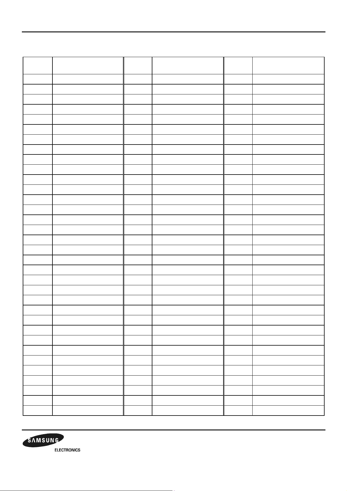
Table 1-4. S3C2440X Special Registers (Sheet 1 of 14)
Register
Name
Address
(B. Endian)
Address
(L. Endian)
Acc.
Unit
Read/
Write
Function
Memory Controller
BWSCON 0x48000000
←
W R/W Bus Width & Wait Status Control
BANKCON0 0x48000004 Boot ROM Control
BANKCON1 0x48000008 BANK1 Control
BANKCON2 0x4800000C BANK2 Control
BANKCON3 0x48000010 BANK3 Control
BANKCON4 0x48000014 BANK4 Control
BANKCON5 0x48000018 BANK5 Control
BANKCON6 0x4800001C BANK6 Control
BANKCON7 0x48000020 BANK7 Control
REFRESH 0x48000024 DRAM/SDRAM Refresh Control
BANKSIZE 0x48000028 Flexible Bank Size
MRSRB6 0x4800002C Mode register set for SDRAM BANK6
MRSRB7 0x48000030 Mode register set for SDRAM BANK7
Preliminary product information describes products that are in development,
for which full characterization data and associated errata are not yet available
Specifications and information herein are subject to change without notice.
1-27
Page 28
2003.10.15
PRODUCT OVERVIEW S3C2440X
Table 1-4. S3C2440X Special Registers (Sheet 2 of 14)
Register Name Address
(B. Endian)
Address
(L. Endian)
Acc.
Unit
Read/
Write
Function
USB Host Controller
HcRevision 0x49000000
←
W Control and Status Group
HcControl 0x49000004
HcCommonStatus 0x49000008
HcInterruptStatus 0x4900000C
HcInterruptEnable 0x49000010
HcInterruptDisable 0x49000014
HcHCCA 0x49000018 Memory Pointer Group
HcPeriodCuttentED 0x4900001C
HcControlHeadED 0x49000020
HcControlCurrentED 0x49000024
HcBulkHeadED 0x49000028
HcBulkCurrentED 0x4900002C
HcDoneHead 0x49000030
HcRmInterval 0x49000034 Frame Counter Group
HcFmRemaining 0x49000038
HcFmNumber 0x4900003C
HcPeriodicStart 0x49000040
HcLSThreshold 0x49000044
HcRhDescriptorA 0x49000048 Root Hub Group
HcRhDescriptorB 0x4900004C
HcRhStatus 0x49000050
HcRhPortStatus1 0x49000054
HcRhPortStatus2 0x49000058
Interrupt Controller
SRCPND 0X4A000000
←
W R/W Interrupt Request Status
INTMOD 0X4A000004 W Interrupt Mode Control
INTMSK 0X4A000008 R/W Interrupt Mask Control
PRIORITY 0X4A00000C W IRQ Priority Control
INTPND 0X4A000010 R/W Interrupt Request Status
INTOFFSET 0X4A000014 R Interrupt request source offset
SUBSRCPND 0X4A000018 R/W Sub source pending
INTSUBMSK 0X4A00001C R/W Interrupt sub mask
1-28
Preliminary product information describes products that are in development,
for which full characterization data and associated errata are not yet available
Specifications and information herein are subject to change without notice.
Page 29
2003.10.15
S3C2440X PRODUCT OVERVIEW
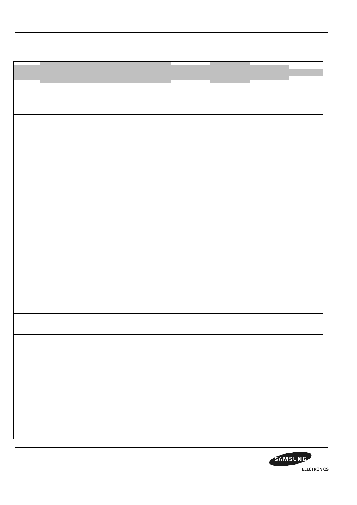
Table 1-4. S3C2440X Special Registers (Sheet 3 of 14)
Register
Name
Address
(B. Endian)
Address
(L. Endian)
Acc.
Unit
Read/
Write
Function
DMA
DISRC0 0x4B000000
←
W R/W DMA 0 Initial Source
DISRCC0 0x4B000004 DMA 0 Initial Source Control
DIDST0 0x4B000008 DMA 0 Initial Destination
DIDSTC0 0x4B00000C DMA 0 Initial Destination Control
DCON0 0x4B000010 DMA 0 Control
DSTAT0 0x4B000014 R DMA 0 Count
DCSRC0 0x4B000018 DMA 0 Current Source
DCDST0 0x4B00001C DMA 0 Current Destination
DMASKTRIG0 0x4B000020 R/W DMA 0 Mask Trigger
DISRC1 0x4B000040 DMA 1 Initial Source
DISRCC1 0x4B000044 DMA 1 Initial Source Control
DIDST1 0x4B000048 DMA 1 Initial Destination
DIDSTC1 0x4B00004C DMA 1 Initial Destination Control
DCON1 0x4B000050 DMA 1 Control
DSTAT1 0x4B000054 R DMA 1 Count
DCSRC1 0x4B000058 DMA 1 Current Source
DCDST1 0x4B00005C DMA 1 Current Destination
DMASKTRIG1 0x4B000060 R/W DMA 1 Mask Trigger
DISRC2 0x4B000080 DMA 2 Initial Source
DISRCC2 0x4B000084 DMA 2 Initial Source Control
DIDST2 0x4B000088 DMA 2 Initial Destination
DIDSTC2 0x4B00008C DMA 2 Initial Destination Control
DCON2 0x4B000090 DMA 2 Control
DSTAT2 0x4B000094 R DMA 2 Count
DCSRC2 0x4B000098 DMA 2 Current Source
DCDST2 0x4B00009C DMA 2 Current Destination
DMASKTRIG2 0x4B0000A0 R/W DMA 2 Mask Trigger
DISRC3 0x4B0000C0
←
W R/W DMA 3 Initial Source
DISRCC3 0x4B0000C4 DMA 3 Initial Source Control
DIDST3 0x4B0000C8 DMA 3 Initial Destination
DIDSTC3 0x4B0000CC DMA 3 Initial Destination Control
DCON3 0x4B0000D0 DMA 3 Control
DSTAT3 0x4B0000D4 R DMA 3 Count
DCSRC3 0x4B0000D8 DMA 3 Current Source
DCDST3 0x4B0000DC DMA 3 Current Destination
DMASKTRIG3 0x4B0000E0 R/W DMA 3 Mask Trigger
Preliminary product information describes products that are in development,
for which full characterization data and associated errata are not yet available
Specifications and information herein are subject to change without notice.
1-29
Page 30
2003.10.15
PRODUCT OVERVIEW S3C2440X
Table 1-4. S3C2440X Special Registers (Sheet 4 of 14)
Register
Name
Address
(B. Endian)
Address
(L. Endian)
Acc.
Unit
Read/
Write
Function
Clock & Power Management
LOCKTIME 0x4C000000
←
W R/W PLL Lock Time Counter
MPLLCON 0x4C000004 MPLL Control
UPLLCON 0x4C000008 UPLL Control
CLKCON 0x4C00000C Clock Generator Control
CLKSLOW 0x4C000010 Slow Clock Control
CLKDIVN 0x4C000014 Clock divider Control
CAMDIVN 0x4C000018 Camera Clock divider Control
LCD Controller
LCDCON1 0X4D000000
←
W R/W LCD Control 1
LCDCON2 0X4D000004 LCD Control 2
LCDCON3 0X4D000008 LCD Control 3
LCDCON4 0X4D00000C LCD Control 4
LCDCON5 0X4D000010 LCD Control 5
LCDSADDR1 0X4D000014 STN/TFT: Frame Buffer Start
Address1
LCDSADDR2 0X4D000018 STN/TFT: Frame Buffer Start
Address2
LCDSADDR3 0X4D00001C STN/TFT: Virtual Screen Address Set
REDLUT 0X4D000020 STN: Red Lookup Table
GREENLUT 0X4D000024 STN: Green Lookup Table
BLUELUT 0X4D000028 STN: Blue Lookup Table
DITHMODE 0X4D00004C STN: Dithering Mode
TPAL 0X4D000050 TFT: Temporary Palette
LCDINTPND 0X4D000054 LCD Interrupt Pending
LCDSRCPND 0X4D000058 LCD Interrupt Source
LCDINTMSK 0X4D00005C LCD Interrupt Mask
TCONSEL 0X4D000060 TCON(LPC3600/LCC3600) Control
1-30
Preliminary product information describes products that are in development,
for which full characterization data and associated errata are not yet available
Specifications and information herein are subject to change without notice.
Page 31

2003.10.15
S3C2440X PRODUCT OVERVIEW
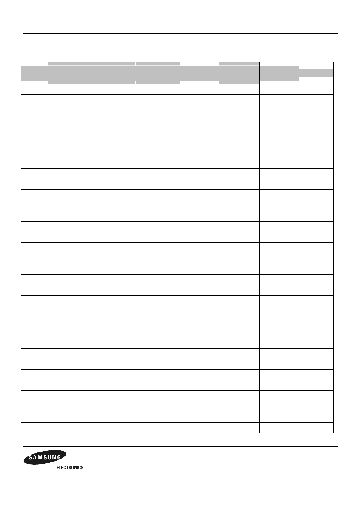
Table 1-4. S3C2440X Special Registers (Sheet 5 of 14)
Register
Name
Address
(B. Endian)
Address
(L. Endian)
Acc.
Unit
Read/
Write
Function
NAND Flash
NFCONF 0x4E000000
←
W R/W NAND Flash Configuration
NFCONT 0x4E000004 NAND Flash Control
NFCMD 0x4E000008 NAND Flash Command
NFADDR 0x4E00000C NAND Flash Address
NFDATA 0x4E000010 NAND Flash Data
NFMECC0 0x4E000014 NAND Flash Main area ECC0/1
NFMECC1 0x4E000018 NAND Flash Main area ECC2/3
NFSECC 0x4E00001C NAND Flash Spare area ECC
NFSTAT 0x4E000020 NAND Flash Operation Status
NFESTAT0 0x4E000024 NAND Flash ECC Status for I/O[7:0]
NFESTAT1 0x4E000028 NAND Flash ECC Status for I/O[15:8]
NFMECC0 0x4E00002C R NAND Flash Main area ECC0 status
NFMECC1 0x4E000030 NAND Flash Main Area ECC1 status
NFSECC 0x4E000034 NAND Flash Spare Area ECC status
NFSBLK 0x4E000038 R/W NAND Flash start block address
NFEBLK 0x4E00003C NAND Flash end block address
Preliminary product information describes products that are in development,
for which full characterization data and associated errata are not yet available
Specifications and information herein are subject to change without notice.
1-31
Page 32

2003.10.15
PRODUCT OVERVIEW S3C2440X
Table 1-4. S3C2440X Special Registers (Sheet 6 of 14)
Register
Name
Address
(B. Endian)
Address
(L. Endian)
Acc.
Unit
Read/
Write
Function
Camera Interface
ASIZE 0x4F000000
←
W W A-port Im age Size
STAY1 0x4F000004 R/W Y start address for 1stping-pong memory of A-
port Image
STAY2 0x4F000008 Y start address for 2ndping-pong memory of A-
port Image
STAY3 0x4F00000C Y start address for 3rdping-pong memory of A-
port Image
STAY4 0x4F000010 Y start address for 4thping-pong memory of A-
port Image
AYBURST 0x4F000014 W A-port Image Y data burst length
ACBBURST 0x4F000018 A-port Image Cb data burst length
ACRBURST 0x4F00001C A-port Image Cr data burst length
BSIZE 0x4F000020 B-port Image Size
STBY1 0x4F000024 Y start address for 1stping-pong memory of B-
port Image
STBY2 0x4F000028 Y start address for 2ndping-pong memory of B-
port Image
STBY3 0x4F00002C Y start address for 3rdping-pong memory of B-
port Image
STBY4 0x4F000030 Y start address for 4thping-pong memory of B-
port Image
BYBURST 0x4F000034 B-port Image Y data burst length
BCBBURST 0x4F000038 B-port Image Cb data burst length
BCRBURST 0x4F00003C B-port Image Cr data burst length
ADISTWIDTH 0x4F000040 A Last HREF Distance Width
BDISTWIDTH 0x4F000044 B Last HREF Distance Width
YRATIO 0x4F00004C Y Scale Ratio
CRATIO 0x4F000050 C Scale Ratio
YORIGINAL 0x4F000054 Y Original Size
CORIGINAL 0x4F00005C C Original Size
STACB1 0x4F000074 A Cb 1 Start Address
STACB2 0x4F000078 A Cb 2 Start Address
STACB3 0x4F00007C A Cb 3 Start Address
STACB4 0x4F000080 A Cb 4 Start Address
1-32
Preliminary product information describes products that are in development,
for which full characterization data and associated errata are not yet available
Specifications and information herein are subject to change without notice.
Page 33

2003.10.15
S3C2440X PRODUCT OVERVIEW
Table 1-4. S3C2440X Special Registers (Sheet 7 of 14)
Register
Name
Address
(B. Endian)
Address
(L. Endian)
Acc.
Unit
Read/
Write
Function
Camera Interface(Continued)
STACR1 0x4F000084
←
W W A Cr 1 Start Address
STACR2 0x4F000088 A Cr 2 Start Address
STACR3 0x4F00008C A Cr 3 Start Address
STACR4 0x4F000090 A Cr 4 Start Address
STBCB1 0x4F00009C B Cb 1 Start Address
STBCB2 0x4F0000A0 B Cb 2 Start Address
STBCB3 0x4F0000A4 B Cb 3 Start Address
STBCB4 0x4F0000A8 B Cb 4 Start Address
STBCR1 0x4F0000AC B Cr 1 Start Address
STBCR2 0x4F0000B0 B Cr 2 Start Address
STBCR3 0x4F0000B4 B Cr 3 Start Address
STBCR4 0x4F0000B8 B Cr 4 Start Address
CTRL 0x4F0000BC Control Register
RDSTAT 0x4F000000 R Status Read Register
RDSTAY 0x4F000014 A Y Start Address Read
RDSTACB 0x4F000018 A Cb Start Address Read
RDSTACR 0x4F00001C A Cr Start Address Read
RDSTACB1 0x4F000020 A Cb1 Start Address Read
RDSTACR1 0x4F000024 A Cr1 Start Address Read
RDSTBY1 0x4F000028 B Y1 Start Address Read
RDSTBY2 0x4F00002C B Y2 Start Address Read
RDSTBY3 0x4F000030 B Y3 Start Address Read
RDSTBY4 0x4F000034 B Y4 Start Address Read
RDSTBY 0x4F000038 B Y Start Address Read
RDSTBCB 0x4F00003C B Cb Start Address Read
RDSTBCR 0x4F000040 B Cr Start Address Read
RDSTBCB1 0x4F000044 B Cb1 Start Address Read
RDSTBCR1 0x4F000048 B Cr1 Start Address Read
RDADISTWIDTH 0x4F00004C A Last HREF Distance Width
RDBDISTWIDTH 0x4F000050 B Last HREF Distance Width
Preliminary product information describes products that are in development,
for which full characterization data and associated errata are not yet available
Specifications and information herein are subject to change without notice.
1-33
Page 34

2003.10.15
PRODUCT OVERVIEW S3C2440X
Table 1-4. S3C2440X Special Registers (Sheet 8 of 14)
Register
Name
Address
(B. Endian)
Address
(L. Endian)
Acc.
Unit
Read/
Write
Function
UART
ULCON0 0x50000000
←
W R/W UART0LineControl
UCON0 0x50000004 UART 0 Control
UFCON0 0x50000008 UART 0 FIFO Control
UMCON0 0x5000000C UART 0 Modem Control
UTRSTAT0 0x50000010 R UART 0 Tx/Rx Status
UERSTAT0 0x50000014 UART 0 Rx Error Status
UFSTAT0 0x50000018 UART 0 FIFO Status
UMSTAT0 0x5000001C UART 0 Modem Status
UTXH0 0x50000023 0x50000020 B W UART 0 Transmission Hold
URXH0 0x50000027 0x50000024 R UART 0 Receive Buffer
UBRDIV0 0x50000028
←
W R/W UART 0 Baud Rate Divisor
ULCON1 0x50004000 UART 1 Line Control
UCON1 0x50004004 UART 1 Control
UFCON1 0x50004008 UART 1 FIFO Control
UMCON1 0x5000400C UART 1 Modem Control
UTRSTAT1 0x50004010 R UART 1 Tx/Rx Status
UERSTAT1 0x50004014 UART 1 Rx Error Status
UFSTAT1 0x50004018 UART 1 FIFO Status
UMSTAT1 0x5000401C UART 1 Modem Status
UTXH1 0x50004023 0x50004020 B W UART 1 Transmission Hold
URXH1 0x50004027 0x50004024 R UART 1 Receive Buffer
UBRDIV1 0x50004028
←
W R/W UART 1 Baud Rate Divisor
ULCON2 0x50008000 UART 2 Line Control
UCON2 0x50008004 UART 2 Control
UFCON2 0x50008008 UART 2 FIFO Control
UTRSTAT2 0x50008010 R UART 2 Tx/Rx Status
UERSTAT2 0x50008014 UART 2 Rx Error Status
UFSTAT2 0x50008018 UART 2 FIFO Status
UTXH2 0x50008023 0x50008020 B W UART 2 Transmission Hold
URXH2 0x50008027 0x50008024 R UART 2 Receive Buffer
UBRDIV2 0x50008028
←
W R/W UART 2 Baud Rate Divisor
1-34
Preliminary product information describes products that are in development,
for which full characterization data and associated errata are not yet available
Specifications and information herein are subject to change without notice.
Page 35

2003.10.15
S3C2440X PRODUCT OVERVIEW
Table 1-4. S3C2440X Special Registers (Sheet 9 of 14)
Register
Name
Address
(B. Endian)
Address
(L. Endian)
Acc.
Unit
Read/
Write
Function
PWM Timer
TCFG0 0x51000000
←
W R/W Timer Configuration
TCFG1 0x51000004 Timer Configuration
TCON 0x51000008 Timer Control
TCNTB0 0x5100000C Timer Count Buffer 0
TCMPB0 0x51000010 Timer Compare Buffer 0
TCNTO0 0x51000014 R Timer Count Observation 0
TCNTB1 0x51000018 R/W Timer Count Buffer 1
TCMPB1 0x5100001C Timer Compare Buffer 1
TCNTO1 0x51000020 R Timer Count Observation 1
TCNTB2 0x51000024 R/W Timer Count Buffer 2
TCMPB2 0x51000028 Timer Compare Buffer 2
TCNTO2 0x5100002C R Timer Count Observation 2
TCNTB3 0x51000030 R/W Timer Count Buffer 3
TCMPB3 0x51000034 Timer Compare Buffer 3
TCNTO3 0x51000038 R Timer Count Observation 3
TCNTB4 0x5100003C R/W Timer Count Buffer 4
TCNTO4 0x51000040 R Timer Count Observation 4
Preliminary product information describes products that are in development,
for which full characterization data and associated errata are not yet available
Specifications and information herein are subject to change without notice.
1-35
Page 36

2003.10.15
PRODUCT OVERVIEW S3C2440X
Table 1-4. S3C2440X Special Registers (Sheet 10 of 14))
Register Name Address
(B. Endian)
Address
(L. Endian)
Acc.
Unit
Read/W
rite
Function
USB Device
FUNC_ADDR_REG 0x52000143 0x52000140 B R/W Function Address
PWR_REG 0x52000147 0x52000144 Power Management
EP_INT_REG 0x5200014B 0x52000148 EP Interrupt Pending and Clear
USB_INT_REG 0x5200015B 0x52000158 USB Interrupt Pending and Clear
EP_INT_EN_REG 0x5200015F 0x5200015C Interrupt Enable
USB_INT_EN_REG 0x5200016F 0x5200016C Interrupt Enable
FRAME_NUM1_REG 0x52000173 0x52000170 R Frame Number Lower Byte
FRAME_NUM2_REG 0x52000177 0x52000174 Frame Number Higher Byte
INDEX_REG 0x5200017B 0x52000178 R/W Register Index
EP0_CSR 0x52000187 0x52000184 Endpoint 0 Status
IN_CSR1_REG 0x52000187 0x52000184 In Endpoint Control Status
IN_CSR2_REG 0x5200018B 0x52000188 In Endpoint Control Status
MAXP_REG 0x52000183 0x52000180 Endpoint Max Packet
OUT_CSR1_REG 0x52000193 0x52000190 Out Endpoint Control Status
OUT_CSR2_REG 0x52000197 0x52000194 Out Endpoint Control Status
OUT_FIFO_CNT1_REG 0x5200019B 0x52000198 R Endpoint Out Write Count
OUT_FIFO_CNT2_REG 0x5200019F 0x5200019C Endpoint Out Write Count
EP0_FIFO 0x520001C3 0x520001C0 R/W Endpoint 0 FIFO
EP1_FIFO 0x520001C7 0x520001C4 Endpoint 1 FIFO
EP2_FIFO 0x520001CB 0x520001C8 Endpoint 2 FIFO
EP3_FIFO 0x520001CF 0x520001CC Endpoint 3 FIFO
EP4_FIFO 0x520001D3 0x520001D0 Endpoint 4 FIFO
EP1_DMA_CON 0x52000203 0x52000200 EP1 DMA Interface Control
EP1_DMA_UNIT 0x52000207 0x52000204 EP1 DMA Tx Unit Counter
EP1_DMA_FIFO 0x5200020B 0x52000208 EP1 DMA Tx FIFO Counter
EP1_DMA_TTC_L 0x5200020F 0x5200020C EP1 DMA Total Tx Counter
EP1_DMA_TTC_M 0x52000213 0x52000210 EP1 DMA Total Tx Counter
EP1_DMA_TTC_H 0x52000217 0x52000214 EP1 DMA Total Tx Counter
1-36
Preliminary product information describes products that are in development,
for which full characterization data and associated errata are not yet available
Specifications and information herein are subject to change without notice.
Page 37

2003.10.15
S3C2440X PRODUCT OVERVIEW
Table 1-4. S3C2440X Special Registers (Sheet 11 of 14)
Register Name Address
(B. Endian)
Address
(L. Endian)
Acc.
Unit
Read/W
rite
Function
USB Device (Continued)
EP2_DMA_CON 0x5200021B 0x52000218 B R/W EP2 DMA Interface Control
EP2_DMA_UNIT 0x5200021F 0x5200021C EP2 DMA Tx Unit Counter
EP2_DMA_FIFO 0x52000223 0x52000220 EP2 DMA Tx FIFO Counter
EP2_DMA_TTC_L 0x52000227 0x52000224 EP2 DMA Total Tx Counter
EP2_DMA_TTC_M 0x5200022B 0x52000228 EP2 DMA Total Tx Counter
EP2_DMA_TTC_H 0x5200022F 0x5200022C EP2 DMA Total Tx Counter
EP3_DMA_CON 0x52000243 0x52000240 EP3 DMA Interface Control
EP3_DMA_UNIT 0x52000247 0x52000244 EP3 DMA Tx Unit Counter
EP3_DMA_FIFO 0x5200024B 0x52000248 EP3 DMA Tx FIFO Counter
EP3_DMA_TTC_L 0x5200024F 0x5200024C EP3 DMA Total Tx Counter
EP3_DMA_TTC_M 0x52000253 0x52000250 EP3 DMA Total Tx Counter
EP3_DMA_TTC_H 0x52000257 0x52000254 EP3 DMA Total Tx Counter
EP4_DMA_CON 0x5200025B 0x52000258 EP4 DMA Interface Control
EP4_DMA_UNIT 0x5200025F 0x5200025C EP4 DMA Tx Unit Counter
EP4_DMA_FIFO 0x52000263 0x52000260 EP4 DMA Tx FIFO Counter
EP4_DMA_TTC_L 0x52000267 0x52000264 EP4 DMA Total Tx Counter
EP4_DMA_TTC_M 0x5200026B 0x52000268 EP4 DMA Total Tx Counter
EP4_DMA_TTC_H 0x5200026F 0x5200026C EP4 DMA Total Tx Counter
Watchdog Timer
WTCON 0x53000000
←
W R/W Watchdog Timer Mode
WTDAT 0x53000004 Watchdog Timer Data
WTCNT 0x53000008 Watchdog Timer Count
IIC
IICCON 0x54000000
←
W R/W IIC Control
IICSTAT 0x54000004 IIC Status
IICADD 0x54000008 IIC Address
IICDS 0x5400000C IIC Data Shift
IICLC 0x54000010 IIC multi-master line control
IIS
IISCON 0x55000000,02 0x55000000 HW,W R/W IIS Control
IISMOD 0x55000004,06 0x55000004 IIS Mode
IISPSR 0x55000008,0A 0x55000008 IIS Prescaler
IISFCON 0x5500000C,0E 0x5500000C IIS FIFO Control
IISFIFO 0x55000012 0x55000010 HW IIS FIFO Entry
Preliminary product information describes products that are in development,
for which full characterization data and associated errata are not yet available
Specifications and information herein are subject to change without notice.
1-37
Page 38

2003.10.15
PRODUCT OVERVIEW S3C2440X
Table 1-4. S3C2440X Special Registers (Sheet 12 of 14)
Register
Name
Address
(B. Endian)
Address
(L.
Acc.
Unit
Read/
Write
Function
Endian)
I/O port
GPACON 0x56000000
←
W R/W Port A Control
GPADAT 0x56000004 Port A Data
GPBCON 0x56000010 Port B Control
GPBDAT 0x56000014 Port B Data
GPBUP 0x56000018 Pull-up Control B
GPCCON 0x56000020 Port C Control
GPCDAT 0x56000024 Port C Data
GPCUP 0x56000028 Pull-up Control C
GPDCON 0x56000030 Port D Control
GPDDA1T 0x56000034 Port D Data
GPDUP 0x56000038 Pull-up Control D
GPECON 0x56000040 Port E Control
GPEDAT 0x56000044 Port E Data
GPEUP 0x56000048 Pull-up Control E
GPFCON 0x56000050 Port F Control
GPFDAT 0x56000054 Port F Data
GPFUP 0x56000058 Pull-up Control F
GPGCON 0x56000060 Port G Control
GPGDAT 0x56000064 Port G Data
GPGUP 0x56000068 Pull-up Control G
GPHCON 0x56000070 Port H Control
GPHDAT 0x56000074 Port H Data
GPHUP 0x56000078 Pull-up Control H
GPJCON 0x560000D0 Port J Control
GPJDAT 0x560000D4 Port J Data
GPJUP 0x560000D8 Pull-up Control J
MISCCR 0x56000080 Miscellaneous Control
DCLKCON 0x56000084 DCLK0/1 Control
EXTINT0 0x56000088 External Interrupt Control Register 0
EXTINT1 0x5600008C External Interrupt Control Register 1
EXTINT2 0x56000090 External Interrupt Control Register 2
1-38
Preliminary product information describes products that are in development,
for which full characterization data and associated errata are not yet available
Specifications and information herein are subject to change without notice.
Page 39

2003.10.15
S3C2440X PRODUCT OVERVIEW
Table 1-4. S3C2440X Special Registers (Sheet 13 of 14)
Register
Name
Address
(B. Endian)
Address
(L. Endian)
Acc.
Unit
Read/
Write
Function
I/O port (Continued)
EINTFLT0 0x56000094
←
WR/WReserved
EINTFLT1 0x56000098 Reserved
EINTFLT2 0x5600009C External Interrupt Filter Control Register 2
EINTFLT3 0x560000A0 External Interrupt Filter Control Register 3
EINTMASK 0x560000A4 External Interrupt Mask
EINTPEND 0x560000A8 External Interrupt Pending
GSTATUS0 0x560000AC
R
External Pin Status
GSTATUS1 0x560000B0 R/W Chip ID
GSTATUS2 0x560000B4 Reset Status
GSTATUS3 0x560000B8 Inform Register
GSTATUS4 0x560000BC Inform Register
MSLCON 0x560000CC Memory Sleep Control Register
RTC
RTCCON 0x57000043 0x57000040 B R/W RTC Control
TICNT 0x57000047 0x57000044 Tick time count
RTCALM 0x57000053 0x57000050 RTC Alarm Control
ALMSEC 0x57000057 0x57000054 Alarm Second
ALMMIN 0x5700005B 0x57000058 Alarm Minute
ALMHOUR 0x5700005F 0x5700005C Alarm Hour
ALMDATE 0x57000063 0x57000060 Alarm Day
ALMMON 0x57000067 0x57000064 Alarm Month
ALMYEAR 0x5700006B 0x57000068 Alarm Year
RTCRST 0x5700006F 0x5700006C RTC Round Reset
BCDSEC 0x57000073 0x57000070 BCD Second
BCDMIN 0x57000077 0x57000074 BCD Minute
BCDHOUR 0x5700007B 0x57000078 BCD Hour
BCDDATE 0x5700007F 0x5700007C BCD Day
BCDDAY 0x57000083 0x57000080 BCD Date
BCDMON 0x57000087 0x57000084 BCD Month
BCDYEAR 0x5700008B 0x57000088 BCD Year
Preliminary product information describes products that are in development,
for which full characterization data and associated errata are not yet available
Specifications and information herein are subject to change without notice.
1-39
Page 40

2003.10.15
PRODUCT OVERVIEW S3C2440X
Table 1-4. S3C2440X Special Registers (Sheet 14 of 14)
Register
Name
Address
(B. Endian)
Address
(L. Endian)
Acc. Unit Read/
Write
Function
A/D converter
ADCCON 0x58000000
←
W R/W ADC Control
ADCTSC 0x58000004 ADC Touch Screen Control
ADCDLY 0x58000008 ADC Start or Interval Delay
ADCDAT0 0x5800000C R ADC Conversion Data
ADCDAT1 0x58000010 ADC Conversion Data
ADCUPDN 0x58000014 R/W Stylus Up or Down Interrpt status
SPI
SPCON0,1 0x59000000,20
←
W R/W SPI Control
SPSTA0,1 0x59000004,24 R SPI Status
SPPIN0,1 0x59000008,28 R/W SPI Pin Control
SPPRE0,1 0x5900000C,2C SPI Baud Rate Prescaler
SPTDAT0,1 0x59000010,30 SPI Tx Data
SPRDAT0,1 0x59000014,34 R SPI Rx Data
SD interface
SDICON 0x5A000000
←
W R/W SDI Control
SDIPRE 0x5A000004 SDI Baud Rate Prescaler
SDICARG 0x5A000008 SDI Command Argument
SDICCON 0x5A00000C SDI Command Control
SDICSTA 0x5A000010 R/(C) SDI Command Status
SDIRSP0 0x5A000014 R SDI Response
SDIRSP1 0x5A000018 SDI Response
SDIRSP2 0x5A00001C SDI Response
SDIRSP3 0x5A000020 SDI Response
SDIDTIMER 0x5A000024 R/W SDI Data / Busy Timer
SDIBSIZE 0x5A000028 SDI Block Size
SDIDCON 0x5A00002C SDI Data control
SDIDCNT 0x5A000030 R SDI Data Remain Counter
SDIDSTA 0x5A000034 R/(C) SDI Data Status
SDIFSTA 0x5A000038 R SDI FIFO Status
SDIDAT 0x5A00003F 0x5A00003C B R/W SDI Data
SDIIMSK 0x5A000040
←
W SDI Interrupt Mask
1-40
Preliminary product information describes products that are in development,
for which full characterization data and associated errata are not yet available
Specifications and information herein are subject to change without notice.
Page 41

2003.09.25
PRODUCT OVERVIEW S3C2440X
Table 1-4. S3C2440X Special Registers (Sheet of 14 of 14)
Register
Name
Address
(B. Endian)
Address
(L. Endian)
Acc. Unit Read/
Write
Function
A/D converter
ADCCON 0x58000000
←
W R/W ADC Control
ADCTSC 0x58000004 ADC Touch Screen Control
ADCDLY 0x58000008 ADC Start or Interval Delay
ADCDAT0 0x5800000C R ADC Conversion Data
ADCDAT1 0x58000010 ADC Conversion Data
ADCUPDN 0x58000014 R/W Stylus Up or Down Interrpt status
SPI
SPCON0,1 0x59000000,20
←
W R/W SPI Control
SPSTA0,1 0x59000004,24 R SPI Status
SPPIN0,1 0x59000008,28 R/W SPI Pin Control
SPPRE0,1 0x5900000C,2C SPI Baud Rate Prescaler
SPTDAT0,1 0x59000010,30 SPI Tx Data
SPRDAT0,1 0x59000014,34 R SPIRx Data
SD interface
SDICON 0x5A000000
←
W R/W SDI Control
SDIPRE 0x5A000004 SDI Baud Rate Prescaler
SDICARG 0x5A000008 SDI Command Argument
SDICCON 0x5A00000C SDI Command Control
SDICSTA 0x5A000010 R/(C) SDI Command Status
SDIRSP0 0x5A000014 R SDI Response
SDIRSP1 0x5A000018 SDI Response
SDIRSP2 0x5A00001C SDI Response
SDIRSP3 0x5A000020 SDI Response
SDIDTIMER 0x5A000024 R/W SDI Data / Busy Timer
SDIBSIZE 0x5A000028 SDI Block Size
SDIDCON 0x5A00002C SDI Data control
SDIDCNT 0x5A000030 R SDI Data Remain Counter
SDIDSTA 0x5A000034 R/(C) SDI Data Status
SDIFSTA 0x5A000038 R SDI FIFO Status
SDIDAT 0x5A00003F 0x5A00003C B R/W SDI Data
SDIIMSK 0x5A000040
←
W SDI Interrupt Mask
1-40
Preliminary product information describes products that are in development,
for which full characterization data and associated errata are not yet available
Specifications and information herein are subject to change without notice.
Page 42

2003.09.25
S3C2440X RISC MICROPROCESSOR MEMORY CONTROLLER
5 MEMORY CONTROLLER
OVERVIEW
The S3C2440X memory controller provides memory control signals that are required for external memory access.
The S3C2440X has the following features:
— Little/Big endian (selectable by a software)
— Address space: 128Mbytes per bank (total 1GB/8 banks)
— Programmable access size (8/16/32-bit) for all banks except bank0 (16/32-bit)
— Total 8 memory banks
Six memory banks for ROM, SRAM, etc.
Remaining two memory banks for ROM, SRAM, SDRAM, etc .
— Seven fixed memory bank start address
— One flexible memory bank start address and programmable bank size
— Programmable access cycles for all memory banks
— External wait to extend the bus cycles
— Supporting self-refresh and power down mode in SDRAM
Preliminary product information describes products that are in development,
for which full characterization data and associated errata are not yet available
Specifications and information herein are subject to change without notice.
5-1
Page 43

2003.09.25
MEMORY CONTROLLER S3C2440X RISC MICROPROCESSOR
0x40000_0000
0x3800_0000
0x3000_0000
0x2800_0000
0x2000_0000
0x1800_0000
0x1000_0000
0x0800_0000
0x0000_0000
OM[1:0] = 01,10
SROM/SDRAM
(nGCS 7)
SROM/SDRAM
(nGCS 6)
SROM
(nGCS 5)
SROM
(nGCS 4)
SROM
(nGCS 3)
SROM
(nGCS 2)
SROM
(nGCS 1)
SROM
(nGCS 0)
[ Not using NAND flash for boot ROM ] [ Using NAND flash for boot ROM ]
OM[1:0]= 00
SROM/SDRAM
(nGCS7)
SROM/SDRAM
(nGCS6)
SROM
(nGCS5)
SROM
(nGCS4)
SROM
(nGCS3)
SROM
(nGCS2)
SROM
(nGCS1)
Boot Internal
SRAM (4KB)
2MB/4MB/8MB/16MB
/32MB/64MB/128MB
}
2MB/4MB/8MB/16MB
/32MB/64MB/128MB
128MB
128MB
HADDR[29:0]
Accessible
128MB
128MB
128MB
128MB
Refer to
Table 5-1
1GB
Region
Note: SROM means ROM or SRAM type memory
Figure 5-1. S3C2440X Memory Map after Reset
Table 5-1. Bank 6/7 Addresses
Address 2MB 4MB 8MB 16MB 32MB 64MB 128MB
Bank 6
Start address
End address
0x3000_0000 0x3000_0000 0x3000_0000 0x3000_0000 0x3000_0000 0x3000_0000 0x3000_0000
0x301F_FFFF 0X303F_FFFF 0X307F_FFFF 0X30FF_FFFF 0X31FF_FFFF 0X33FF_FFFF 0X37FF_FFFF
Bank 7
Start address
End address
Note: Bank 6 and 7 must have the same memory size.
0x3020_0000 0x3040_0000 0x3080_0000 0x3100_0000 0x3200_0000 0x3400_0000 0x3800_0000
0X303F_FFFF 0X307F_FFFF 0X30FF_FFFF 0X31FF_FFFF 0X33FF_FFFF 0X37FF_FFFF 0X3FFF_FFFF
5-2
Preliminary product information describes products that are in development,
for which full characterization data and associated errata are not yet available
Specifications and information herein are subject to change without notice.
Page 44

2003.09.25
S3C2440X RISC MICROPROCESSOR MEMORY CONTROLLER
DEC.13, 2002
FUNCTION DESCRIPTION
BANK0 BUS WIDTH
The data bus of BANK0 (nGCS0) should be configured in width as one of 16-bit and 32-bit ones. Because the
BANK0 works as the booting ROM bank (map to 0x0000_0000), the bus width of BANK0 should be determined
before the first ROM access, which will depend on the logic level of OM[1:0] at Reset.
OM1 (Operating Mode 1) OM0 (Operating Mode 0) Booting ROM Data width
0 0 Nand Flash Mode
0 1 16-bit
1 0 32-bit
1 1 Test Mode
MEMORY (SROM/SDRAM) ADDRESS PIN CONNECTIONS
MEMORY ADDR. PIN S3C2440X ADDR.
@ 8-bit DATA BUS
A0 A0 A1 A2
A1 A1 A2 A3
... ... ... ...
S3C2440X ADDR.
@16-bitDATABUS
S3C2440X ADDR.
@ 32-bit DATA BUS
Preliminary product information describes products that are in development,
for which full characterization data and associated errata are not yet available
Specifications and information herein are subject to change without notice.
5-3
Page 45

2003.09.25
MEMORY CONTROLLER S3C2440X RISC MICROPROCESSOR
SDRAM BANK ADDRESS PIN CONNECTION EXAMPLE
Table 5-2. SDRAM Bank Address Configuration
Bank Size Bus Width Base Component Memory Configuration Bank Address
2MByte x8 16Mbit (1M x 8 x 2Bank) x 1 A20
x16 (512K x 16 x 2B) x 1
4MB x16 (1M x 8 x 2B) x 2 A21
x16 (1Mx8x2B) x2
8MB x16 16Mb (2M x 4 x 2B) x 4 A22
x32 (1Mx8x2B) x4
x8 64Mb (4M x 8 x 2B) x 1
x8 (2M x 8 x 4B) x 1 A[22:21]
x16 (2M x 16 x 2B) x 1 A22
x16 (1M x 16 x 4B) x 1 A[22:21]
x32 (512K x 32 x 4B) x 1
16MB x32 16Mb (2Mx4x2B) x8 A23
x8 64Mb (8M x 4 x 2B) x 2
x8 (4M x 4 x 4B) x 2 A[23:22]
x16 (4Mx8x2B) x2 A23
x16 (2Mx8x4B) x2 A[23:22]
x32 (2M x 16 x 2B) x 2 A23
x32 (1M x 16 x 4B) x 2 A[23:22]
x8 128Mb (4M x 8 x 4B) x 1
x16 (2M x 16 x 4B) x 1
32MB x16 64Mb (8Mx4x2B) x4 A24
x16 (4Mx4x4B) x4 A[24:23]
x32 (4Mx8x2B) x4 A24
x32 (2Mx8x4B) x4 A[24:23]
x16 128Mb (4M x 8 x 4B) x 2
x32 (2M x 16 x 4B) x 2
x8 256Mb (8M x 8 x 4B) x 1
x16 (4M x 16 x 4B) x 1
64MB x32 128Mb (4M x 8 x 4B) x 4 A[25:24]
x16 256Mb (8M x 8 x 4B) x 2
x32 (4M x 16 x 4B) x 2
x8 512Mb (16M x 8 x 4 B) x 1
128MB x32 256Mbit (8M x 8 x 4Bank) x 4 A[26:25]
x8 512Mb (32M x 4 x 4 B) x 2
x16 (16Mx8x4B) x2
x32 (8M x 16 x 4B) x 2
5-4
Preliminary product information describes products that are in development,
for which full characterization data and associated errata are not yet available
Specifications and information herein are subject to change without notice.
Page 46

2003.09.25
S3C2440X RISC MICROPROCESSOR MEMORY CONTROLLER
DEC.13, 2002
nWAIT PIN OPERATION
If the WAIT corresponding to each memory bank is enabled, the nOE duration should be prolonged by the external
nWAIT pin while the memory bank is active. nWAIT is checked from tacc-1. nOE will be deasserted at the next
clock after sampling nWAIT is high. The nWE signal have the same relation with nOE.
HCLK
tRC
ADDR
nGCS
nOE
nWAIT
DATA(R)
Tacs
Tacc=4
Tcos
Delayed
Sampling nWAIT
Figure 5-2. S3C2440X External nWAIT Timing Diagram (Tacc=4)
Preliminary product information describes products that are in development,
for which full characterization data and associated errata are not yet available
Specifications and information herein are subject to change without notice.
5-5
Page 47

2003.09.25
MEMORY CONTROLLER S3C2440X RISC MICROPROCESSOR
nXBREQ/nXBACK Pin Operation
If nXBREQ is asserted, the S3C2440X will respond by lowering nXBACK. If nXBACK=L, the address/data bus and
memory control signals are in Hi-Z state as shown in Table 1-1. When nXBREQ is de-asserted, the nXBACK will
also be de-asserted.
HCLK
SCLK
SCKE, A[24:0]
D[31:0], nGCS
nOE,nWE
nWBE
nXBREQ
nXBACK
1clk
Figure 5-3. S3C2440X nXBREQ/nXBACK Timing Diagram
5-6
Preliminary product information describes products that are in development,
for which full characterization data and associated errata are not yet available
Specifications and information herein are subject to change without notice.
Page 48

2003.09.25
S3C2440X RISC MICROPROCESSOR MEMORY CONTROLLER
DEC.13, 2002
ROM Memory Interface Examples
A1
A2
A3
A4
A5
A6
A7
A8
A9
A10
A11
A12
A13
A14
A15
A16
A0
A1
A2
A3
A4
A5
A6
A7
A8
A9
A10
A11
A12
A13
A14
A15
A0
A1
A2
A3
A4
A5
A6
A7
A8
A9
A10
A11
A12
A13
A14
A15
DQ0
DQ1
DQ2
DQ3
DQ4
DQ5
DQ6
DQ7
nWE
nOE
nCE
Figure 5-4. Memory Interface with 8-bit ROM
A0
A1
A2
A3
A4
A5
A6
A7
A8
A9
A10
A11
A12
A13
A14
A15
DQ0
DQ1
DQ2
DQ3
DQ4
DQ5
DQ6
DQ7
nWE
nOE
nCE
D0
D1
D2
D3
D4
D5
D6
D7
nWBE0
nOE
nGCSn
A10
A11
A12
A13
A14
A15
A16
A1
A2
A3
A4
A5
A6
A7
A8
A9
A0
A1
A2
A3
A4
A5
A6
A7
A8
A9
A10
A11
A12
A13
A14
A15
D0
D1
D2
D3
D4
D5
D6
D7
nWE
nOE
nGCSn
DQ0
DQ1
DQ2
DQ3
DQ4
DQ5
DQ6
DQ7
nWE
nOE
nCE
D8
D9
D10
D11
D12
D13
D14
D15
nWBE1
nOE
nGCSn
Figure 5-5. Memory Interface with 8-bit ROM x 2
Preliminary product information describes products that are in development,
for which full characterization data and associated errata are not yet available
Specifications and information herein are subject to change without notice.
5-7
Page 49

2003.09.25
MEMORY CONTROLLER S3C2440X RISC MICROPROCESSOR
A2
A3
A4
A5
A6
A7
A8
A9
A10
A11
A12
A13
A14
A15
A16
A17
A0
A1
A2
A3
A4
A5
A6
A7
A8
A9
A10
A11
A12
A13
A14
A15
DQ0
DQ1
DQ2
DQ3
DQ4
DQ5
DQ6
DQ7
nWE
nOE
nCE
D0
D1
D2
D3
D4
D5
D6
D7
nWBE0
nOE
nGCSn
A2
A3
A4
A5
A6
A7
A8
A9
A10
A11
A12
A13
A14
A15
A16
A17
A0
A1
A2
A3
A4
A5
A6
A7
A8
A9
A10
A11
A12
A13
A14
A15
DQ0
DQ1
DQ2
DQ3
DQ4
DQ5
DQ6
DQ7
nWE
nOE
nCE
D8
D9
D10
D11
D12
D13
D14
D15
nWBE1
nOE
nGCSn
A2
A3
A4
A5
A6
A7
A8
A9
A10
A11
A12
A13
A14
A15
A16
A17
A0
A1
A2
A3
A4
A5
A6
A7
A8
A9
A10
A11
A12
A13
A14
A15
DQ0
DQ1
DQ2
DQ3
DQ4
DQ5
DQ6
DQ7
nWE
nOE
nCE
D16
D17
D18
D19
D20
D21
D22
D23
nWBE2
nOE
nGCSn
Figure 5-6. Memory Interface w ith 8-bit ROM x 4
A10
A11
A12
A13
A14
A15
A16
A17
A18
A19
A1
A2
A3
A4
A5
A6
A7
A8
A9
A0
A1
A2
A3
A4
A5
A6
A7
A8
A9
A10
A11
A12
A13
A14
A15
A16
A17
A18
DQ0
DQ1
DQ2
DQ3
DQ4
DQ5
DQ6
DQ7
DQ8
DQ9
DQ10
DQ11
DQ12
DQ13
DQ14
DQ15
nWE
nOE
nCE
D0
D1
D2
D3
D4
D5
D6
D7
D8
D9
D10
D11
D12
D13
D14
D15
nWE
nOE
nGCSn
A10
A11
A12
A13
A14
A15
A16
A17
A2
A3
A4
A5
A6
A7
A8
A9
A0
A1
A2
A3
A4
A5
A6
A7
A8
A9
A10
A11
A12
A13
A14
A15
DQ0
DQ1
DQ2
DQ3
DQ4
DQ5
DQ6
DQ7
nWE
nOE
nCE
D24
D25
D26
D27
D28
D29
D30
D31
nWBE3
nOE
nGCSn
5-8
Figure 5-7. Memory Interface w ith 16-bit ROM
Preliminary product information describes products that are in development,
for which full characterization data and associated errata are not yet available
Specifications and information herein are subject to change without notice.
Page 50

2003.09.25
S3C2440X RISC MICROPROCESSOR MEMORY CONTROLLER
DEC.13, 2002
SRAM Memory Interface Examples
A10
A11
A12
A13
A14
A15
A16
A17
A2
A3
A4
A5
A6
A7
A8
A9
A1
A2
A3
A4
A5
A6
A7
A8
A9
A10
A11
A12
A13
A14
A15
A16
A0
A1
A2
A3
A4
A5
A6
A7
A8
A9
A10
A11
A12
A13
A14
A15
DQ0
DQ1
DQ2
DQ3
DQ4
DQ5
DQ6
DQ7
DQ8
DQ9
DQ10
DQ11
DQ12
DQ13
DQ14
DQ15
nWE
nOE
nCS
nUB
nLB
D0
D1
D2
D3
D4
D5
D6
D7
D8
D9
D10
D11
D12
D13
D14
D15
nWE
nOE
nGCSn
nBE1
nBE0
Figure 5-8. Memory I nterface with 16-bit SRAM
A0
A1
A2
A3
A4
A5
A6
A7
A8
A9
A10
A11
A12
A13
A14
A15
DQ0
DQ1
DQ2
DQ3
DQ4
DQ5
DQ6
DQ7
DQ8
DQ9
DQ10
DQ11
DQ12
DQ13
DQ14
DQ15
nWE
nOE
nCS
nUB
nLB
D0
D1
D2
D3
D4
D5
D6
D7
D8
D9
D10
D11
D12
D13
D14
D15
nWE
nOE
nGCSn
nBE1
nBE0
A10
A11
A12
A13
A14
A15
A16
A17
A2
A3
A4
A5
A6
A7
A8
A9
A0
A1
A2
A3
A4
A5
A6
A7
A8
A9
A10
A11
A12
A13
A14
A15
DQ0
DQ1
DQ2
DQ3
DQ4
DQ5
DQ6
DQ7
DQ8
DQ9
DQ10
DQ11
DQ12
DQ13
DQ14
DQ15
nWE
nOE
nCS
nUB
nLB
D16
D17
D18
D19
D20
D21
D22
D13
D24
D25
D26
D27
D28
D29
D30
D31
nWE
nOE
nGCSn
nBE3
nBE2
Figure 5-9. Memory Interface with 16-bit SRAM x 2
Preliminary product information describes products that are in development,
for which full characterization data and associated errata are not yet available
Specifications and information herein are subject to change without notice.
5-9
Page 51

2003.09.25
MEMORY CONTROLLER S3C2440X RISC MICROPROCESSOR
SDRAM Memory Interface Examples
A1
A2
A3
A4
A5
A6
A7
A8
A9
A10
A11
A12
A21
A22
DQM0
DQM1
SCKE
SCLK
A0
A1
A2
A3
A4
A5
A6
A7
A8
A9
A10
A11
BA0
BA1
LDQM
UDQM
SCKE
SCLK
DQ0
DQ1
DQ2
DQ3
DQ4
DQ5
DQ6
DQ7
DQ8
DQ9
DQ10
DQ11
DQ12
DQ13
DQ14
DQ15
nSCS
nSRAS
nSCAS
nWE
D0
D1
D2
D3
D4
D5
D6
D7
D8
D9
D10
D11
D12
D13
D14
D15
nSCS0
nSRAS
nSCAS
nWE
Figure 5-10. Memory Interface with 16-bit SDRAM (4Mx16, 4banks)
A2
A3
A4
A5
A6
A7
A8
A9
A10
A11
A12
A13
A22
A23
DQM0
DQM1
SCKE
SCLK
A0
A1
A2
A3
A4
A5
A6
A7
A8
A9
A10
A11
BA0
BA1
LDQM
UDQM
SCKE
SCLK
DQ0
DQ1
DQ2
DQ3
DQ4
DQ5
DQ6
DQ7
DQ8
DQ9
DQ10
DQ11
DQ12
DQ13
DQ14
DQ15
nSCS
nSRAS
nSCAS
nWE
D0
D1
D2
D3
D4
D5
D6
D7
D8
D9
D10
D11
D12
D13
D14
D15
nSCS0
nSRAS
nSCAS
nWE
A2
A3
A4
A5
A6
A7
A8
A9
A10
A11
A12
A13
A22
A23
DQM2
DQM3
SCKE
SCLK
A0
A1
A2
A3
A4
A5
A6
A7
A8
A9
A10
A11
BA0
BA1
LDQM
UDQM
SCKE
SCLK
DQ0
DQ1
DQ2
DQ3
DQ4
DQ5
DQ6
DQ7
DQ8
DQ9
DQ10
DQ11
DQ12
DQ13
DQ14
DQ15
nSCS
nSRAS
nSCAS
nWE
D16
D17
D18
D19
D20
D21
D22
D23
D24
D25
D26
D27
D28
D29
D30
D31
nSCS0
nSRAS
nSCAS
nWE
Figure 5-11. Memory Interface with 16-bit SDRAM (4Mx16 * 2ea, 4banks)
Note: Refer to Table 5-2 for the Bank Address configurations o f SDRAM.
5-10
Preliminary product information describes products that are in development,
for which full characterization data and associated errata are not yet available
Specifications and information herein are subject to change without notice.
Page 52

2003.09.25
S3C2440X RISC MICROPROCESSOR MEMORY CONTROLLER
DEC.13, 2002
PROGRAMMABLE ACCESS CYCLE
HCLK
A[24:0]
nGCS
nOE
nWE
nWBE
D[31:0](R)
D[31:0] (W)
Tacs
Tcos
Tacc Tacp
Tacs = 1 cycle
Tcos = 1 cycle
Tacc = 3 cycles
Tacp = 2 cycles
Tcoh = 1 cycle
Tcah = 2 cycles
Figure 5-12. S3C2440X nGCS Timing Diagram
Tcah
Tcoh
Preliminary product information describes products that are in development,
for which full characterization data and associated errata are not yet available
Specifications and information herein are subject to change without notice.
5-11
Page 53

2003.09.25
MEMORY CONTROLLER S3C2440X RISC MICROPROCESSOR
MCLK
SCKE
nSCS
nSRAS
nSCAS
ADDR
BA
A10/AP
DATA (CL2)
DATA (CL3)
nWE
Trp
RA
BABA
RA
Trcd
Ca
BA BA BA BA BA
Da
Da
Cb Cc Cd Ce
Db Dc Dd De
Db Dc Dd De
5-12
DQM
Bank
Precharge
Figure 5-13. S3C2440X SDRAM Timing Diagram
Row
Active
Write Read (CL = 2, CL = 3, BL = 1)
Trp = 2 cycle Tcas = 2 cycle
Trcd = 2 cycle Tcp = 2 cycle
Preliminary product information describes products that are in development,
for which full characterization data and associated errata are not yet available
Specifications and information herein are subject to change without notice.
Page 54

2003.09.25
S3C2440X RISC MICROPROCESSOR MEMORY CONTROLLER
DEC.13, 2002
BUS WIDTH & WAIT CONTROL REGISTER (BWSCON)
Register Address R/W Description Reset Value
BWSCON 0x48000000 R/W Bus width & wait status control register 0x000000
BWSCON Bit Description Initial state
ST7 [31] Determine SRAM for using UB/LB for bank 7.
0 = Not using UB/LB (The pins are dedicated nWBE[3:0])
1 = Using UB/LB (The pins are dedicated nBE[3:0])
WS7 [30] Determine WAIT status for bank 7.
0 = WAIT disable 1 = WAIT enable
DW7 [29:28] Determine data bus width for bank 7.
00 = 8-bit 01 = 16-bit, 10 = 32-bit 11 = reserved
ST6 [27] Determine SRAM for using UB/LB for bank 6.
0 = Not using UB/LB (The pins are dedicated nWBE[3:0 )
1 = Using UB/LB (The pins are dedicated nBE[3:0])
WS6 [26] Determine WAIT status for bank 6.
0 = WAIT disable, 1 = WAIT enable
DW6 [25:24] Determine data bus width for bank 6.
00 = 8-bit 01 = 16-bit, 10 = 32-bit 11 = reserved
ST5 [23] Determine SRAM for using UB/LB for bank 5.
0 = Not using UB/LB (The pins are dedicated nWBE[3:0])
1 = Using UB/LB (The pins are dedicated nBE[3:0])
WS5 [22] Determine WAIT status for bank 5.
0 = WAIT disable, 1 = WAIT enable
DW5 [21:20] Determine data bus width for bank 5.
00 = 8-bit 01 = 16-bit, 10 = 32-bit 11 = reserved
ST4 [19] Determine SRAM for using UB/LB for bank 4.
0 = Not using UB/LB (The pins are dedicated nWBE[3:0])
1 = Using UB/LB (The pins are dedicated nBE[3:0])
WS4 [18] Determine WAIT status for bank 4.
0 = WAIT disable 1 = WAIT enable
DW4 [17:16] Determine data bus width for bank 4.
00 = 8-bit 01 = 16-bit, 10 = 32-bit 11 = reserved
ST3 [15] Determine SRAM for using UB/LB for bank 3.
0 = Not using UB/LB (The pins are dedicated nWBE[3:0])
1 = Using UB/LB (The pins are dedicated nBE[3:0])
WS3 [14] Determine WAIT status for bank 3.
0 = WAIT disable 1 = WAIT enable
DW3 [13:12] Determine data bus width for bank 3.
00 = 8-bit 01 = 16-bit, 10 = 32-bit 11 = reserved
ST2 [11] Determine SRAM for using UB/LB for bank 2.
0 = Not using UB/LB (The pins are dedicated nWBE[3:0])
1 = Using UB/LB (The pins are dedicated nBE[3:0].)
0
0
0
0
0
0
0
0
0
0
0
0
0
0
0
0
Preliminary product information describes products that are in development,
for which full characterization data and associated errata are not yet available
Specifications and information herein are subject to change without notice.
5-13
Page 55

2003.09.25
MEMORY CONTROLLER S3C2440X RISC MICROPROCESSOR
BUS WIDTH & WAIT CONTROL REGISTER (BWSCON) (Continued)
WS2 [10] Determine WAIT status for bank 2.
0 = WAIT disable 1 = WAIT enable
DW2 [9:8] Determine data bus width for bank 2.
00 = 8-bit 01 = 16-bit, 10 = 32-bit 11 = reserved
ST1 [7] Determine SRAM for using UB/LB for bank 1.
0 = Not using UB/LB (The pins are dedicated nWBE[3:0])
1 = Using UB/LB (The pins are dedicated nBE[3:0])
WS1 [6] Determine WAIT status for bank 1.
0 = WAIT disable, 1 = WAIT enable
DW1 [5:4] Determine data bus width for bank 1.
00 = 8-bit 01 = 16-bit, 10 = 32-bit 11 = reserved
DW0 [2:1] Indicate data bus width for bank 0 (read only).
01 = 16-bit, 10 = 32-bit
The states are selected by OM[1:0] pins
Reserved [0] Reserve to 0 0
Note:
1. All types of master clock in this memory controller correspond to the bus clock.
For example, HCLK in SRAM is the same as the bus clock, and SCLK in SDRAM is also the same as the bus
clock. In this chapter (Memory Controller), one clock means one bus clock.
2. nBE[3:0] is the 'AND' signal nWBE[3:0] an d nOE.
0
0
0
0
0
-
5-14
Preliminary product information describes products that are in development,
for which full characterization data and associated errata are not yet available
Specifications and information herein are subject to change without notice.
Page 56

2003.09.25
S3C2440X RISC MICROPROCESSOR MEMORY CONTROLLER
DEC.13, 2002
BANK CONTROL REGISTER (BANKCONn: nGCS0-nGCS5)
Register Address R/W Description Reset Value
BANKCON0 0x48000004 R/W Bank 0 control register 0x0700
BANKCON1 0x48000008 R/W Bank 1 control register 0x0700
BANKCON2 0x4800000C R/W Bank 2 control register 0x0700
BANKCON3 0x48000010 R/W Bank 3 control register 0x0700
BANKCON4 0x48000014 R/W Bank 4 control register 0x0700
BANKCON5 0x48000018 R/W Bank 5 control register 0x0700
BANKCONn Bit Description Initial State
Tacs [14:13] Address set-up time before nGCSn
00
00 = 0 clock 01 = 1 clock
10 = 2 clocks 11 = 4 clocks
Tcos [12:11] Chip selection set-up time before nOE
00
00 = 0 clock 01 = 1 clock
10 = 2 clocks 11 = 4 clocks
Tacc [10:8] Access cycle
111
000 = 1 clock 001 = 2 clocks
010 = 3 clocks 011 = 4 clocks
100 = 6 clocks 101 = 8 clocks
110 = 10 clocks 111 = 14 clocks
Note: When nWAIT signal is used, Tacc ≥ 4 clocks.
Tcoh [7:6] Chip selection hold time after nOE
000
00 = 0 clock 01 = 1 clock
10 = 2 clocks 11 = 4 clocks
Tcah [5:4] Address hold time after nGCSn
00
00 = 0 clock 01 = 1 clock
10 = 2 clocks 11 = 4 clocks
Tacp [3:2] Page mode access cycle @ Page mode
00
00 = 2 clocks 01 = 3 clocks
10 = 4 clocks 11 = 6 clocks
PMC [1:0] Page mode configuration
00
00 = normal (1 data) 01 = 4 data
10 = 8 data 11 = 16 data
Preliminary product information describes products that are in development,
for which full characterization data and associated errata are not yet available
Specifications and information herein are subject to change without notice.
5-15
Page 57

2003.09.25
MEMORY CONTROLLER S3C2440X RISC MICROPROCESSOR
BANK CONTROL REGISTER (BANKCONn: nGCS6-nGCS7)
Register Address R/W Description Reset Value
BANKCON6 0x4800001C R/W Bank 6 control register 0x18008
BANKCON7 0x48000020 R/W Bank 7 control register 0x18008
BANKCONn Bit Description Initial State
MT [16:15] Determine the memory type for bank6 and bank7.
11
00 = ROM or SRAM 01 = Reserved (Do not use)
10 = Reserved (Do not use) 11 = Sync. DRAM
Memory Type = ROM or SRAM [MT=00] (15-bit)
Tacs [14:13] Address set-up time before nGCS
00 = 0 clock 01 = 1 clock 10 = 2 clocks 11 = 4 clocks
Tcos [12:11] Chip selection set-up time before nOE
00 = 0 clock 01 = 1 clock 10 = 2 clocks 11 = 4 clocks
Tacc [10:8] Access cycle
000=1clock 001=2clocks
010 = 3 clocks 011 = 4 clocks
100 = 6 clocks 101 = 8 clocks
110 = 10 clocks 111 = 14 clocks
Toch [7:6] Chip selection hold time after nOE
00 = 0 clock 01 = 1 clock
10 = 2 clocks 11 = 4 clocks
Tcah [5:4] Address hold time after nGCSn
00 = 0 clock 01 = 1clock 10 = 2 clocks 11 = 4 clocks
Tacp [3:2]
Page mode access cycle @ Page mode
00 = 2 clocks 01 = 3 clocks
10 = 4 clocks 11 = 6 clocks
PMC [1:0] Page mode configuration
00 = normal (1 data) 01 = 4 consecutive accesses
10 = 8 consecutive accesses 11 = 16 consecutive accesses
Memory Type = SDRAM [MT=11] (4-bit)
00
00
111
00
00
00
00
Trcd [3:2] RAS to CAS delay
00 = 2 clocks 01 = 3 clocks 10 = 4 clocks
SCAN [1:0] Column address number
00 = 8-bit 01 = 9-bit 10= 10-bit
5-16
Preliminary product information describes products that are in development,
for which full characterization data and associated errata are not yet available
Specifications and information herein are subject to change without notice.
10
00
Page 58

2003.09.25
S3C2440X RISC MICROPROCESSOR MEMORY CONTROLLER
DEC.13, 2002
REFRESH CONTROL REGISTER
Register Address R/W Description Reset Value
REFRESH 0x48000024 R/W SDRAM refresh control register 0xac0000
REFRESH Bit Description Initial State
REFEN [23] SDRAM Refresh Enable
1
0 = Disable 1 = Enable (self or CBR/auto refresh)
TREFMD [22] SDRAM Refresh Mode
0
0 = CBR/Auto Refresh 1 = Self Refresh
In self-refresh time, the SDRAM control signals are driven to the
appropriate level.
Trp [21:20] SDRAM RAS pre-charge Time
10
00 = 2 clocks 01 = 3 clocks 10 = 4 clocks 11 = Not support
Trc [19:18] SDRAM RC minimum Time
11
00 = 4 clocks 01 = 5 clocks 10 = 6 clocks 11 = 7 clocks
Reserved [17:16] Not used 00
Reserved [15:11] Not used 0000
Refresh
Counter
[10:0] SDRAM refresh count value. Refer to chapter 6 SDRAM refresh
controller bus priority section.
Refresh period = (2
11
-refresh_count+1)/HCLK
0
Ex) If refresh period is 7.8 us and HCLK is 100 MHz,
the refresh count is as follows:
Refresh count = 2
11
+ 1 - 100x7.8 = 1269
Preliminary product information describes products that are in development,
for which full characterization data and associated errata are not yet available
Specifications and information herein are subject to change without notice.
5-17
Page 59

2003.09.25
MEMORY CONTROLLER S3C2440X RISC MICROPROCESSOR
BANKSIZE REGISTER
Register Address R/W Description Reset Value
BANKSIZE 0x48000028 R/W Flexible bank size register 0x0
BANKSIZE Bit Description Initial State
BURST_EN [7] ARM core burst operation enable.
0 = Disable burst operation.
1 = Enable burst operation.
Reserved [6] Not used 0
SCKE_EN [5]
SDRAM power down mode enable control by SCKE
0 = SDRAM power down mode disable
1 = SDRAM power down mode enable
SCLK_EN [4] SCLK is enabled only during SDRAM access cycle for
reducing power consumption. When SDRAM is not accessed,
SCLK becomes 'L' level.
0 = SCLK is always active.
1 = SCLK is active only during the access (recommended).
Reserved [3] Not used 0
BK76MAP [2:0] BANK6/7 memory map
010
010 = 128MB/128MB 001 = 64MB/64MB
000 = 32M/32M 111 = 16M/16M
110 = 8M/8M 101 = 4M/4M
100 = 2M/2M
0
0
0
5-18
Preliminary product information describes products that are in development,
for which full characterization data and associated errata are not yet available
Specifications and information herein are subject to change without notice.
Page 60

2003.09.25
S3C2440X RISC MICROPROCESSOR MEMORY CONTROLLER
DEC.13, 2002
SDRAM MODE REGISTER SET REGISTER (MRSR)
Register Address R/W Description Reset Value
MRSRB6 0x4800002C R/W Mode register set register bank6 xxx
MRSRB7 0x48000030 R/W Mode register set register bank7 xxx
MRSR Bit Description Initial State
Reserved [11:10] Not used WBL [9] Write burst length
x
0: Burst (Fixed)
1: Reserved
TM [8:7] Test mode
xx
00: Mode register set (Fixed)
01, 10 and 11: Reserved
CL [6:4] CAS latency
xxx
000 = 1 clock, 010 = 2 clocks, 011=3 clocks
Others: reserved
BT [3] Burst type
x
0: Sequential (Fixed)
1: Reserved
BL [2:0] Burst length
xxx
000: 1 (Fixed)
Others: Reserved
Note: MRSR regis ter must not be reconfigured while the code is running on SDRAM.
Important Note: In Sleep mode, SDRAM has to enter SDRAM self-refresh mode.
Preliminary product information describes products that are in development,
for which full characterization data and associated errata are not yet available
Specifications and information herein are subject to change without notice.
5-19
Page 61

2003.09.25
MEMORY CONTROLLER S3C2440X RISC MICROPROCESSOR
NOTES
5-20
Preliminary product information describes products that are in development,
for which full characterization data and associated errata are not yet available
Specifications and information herein are subject to change without notice.
Page 62

2003.09.25
S3C2440XRISC MICROPROCESSOR NAND FLASH CONTROLLER
NAND FLASH CONTORLLER
OVERVIEW
In recent times, NOR flash memory gets high in price while an SDRAM and a NAND flash memory get moderate,
motivating some users to execute the boot code on a NAND flash and execute the main code on an SDRAM.
S3C2440X boot code can be executed on an external NAND flash memory. In order to support NAND flash boot
loader, the S3C2440X is equipped with an internal SRAM buffer called ‘Steppingstone’. When booting, the first 4
KBytes of the NAND flash memory will be loaded into Steppingstone and the boot code loaded into Steppingstone
will be executed.
Generally, t he boot code will copy NAND flash content to SDRAM. Using hardware ECC, the NAND flash data
validity will be checked. Upon the completion of the copy, the main pr ogram will be executed on the SDRAM.
FEATURES
1) Auto boot: The boot code is transferred into 4-kbytes Steppingstone during reset. After the transfer, the boot
code will be executed on the Steppingstone.
2) NAND Flash memory I/F: Support 256Words, 512Bytes, 1KWords and 2KBytes Page.
3) Software mode: User can directly access NAND flash memory, for example this feature can be used in
read/erase/program NAND flash memory.
4) Interface: 8 / 16-bit NAND flash memory interface bus.
5) Hardware ECC generation, detection and indication (Software correction).
6) SFR I/F: Support Little Endian Mode, Byte/half word/word access to Data and ECC Data register, and Word
access to other registers
7) SteppingStone I/F: Support Little/Big Endian, Byte/half word/word access.
8) The Steppingstone 4-KB internal SRAM buffer can be used for another purpose after NAND flash booting.
Preliminary product information describes products that are in development,
for which full characterization data and associated errata are not yet available
Specifications and information herein are subject to change without notice.
6-1
Page 63

2003.09.25
NAND FLASH CONTROLLER S3C2440XRISC MICROPROCESSOR
BLOCK DIAGRAM
nFCE
ljj nU
zmy
j M
z t
hoi
z pVm
SYSTEM BUS
uhuk mshzo
p
CLE
ALE
nRE
nWE
R/nB
I/O0 - I/O15
BOOT LOADER FUNCTION
CORE ACCESS
(Boot Code)
USER ACCESS
z z
j
z z
Figure 6-1 NAND Flash Controller Block Diagram
REGISTERS
z z
O[ri iP
z m
y
AUTO BOOT
uhuk mshzo
j
O[ri zyhtP
uhuk mshzo
t
Figure 6-2 NAND Flash Controller Boot Loader Block Diagram
During reset, Nand flash controller will get inf ormation about connected NAND f lash through Pin status(NCON(Adv
flash), GPG13(Page size), GPG14(Address cycle), GPG15(Bus width) – refer to PIN CONFIGURATION), After
power-on or system reset is occurred, the NAND Flash cont roller load automaticallythe 4-KBytes boot loader
codes. After loading the boot loader codes, the boot loader code in steppingstone is executed.
NOTE : During the auto boot, the ECC is not checked. So, the first 4-KB of NAND flash should have no bit error.
6-2
Preliminary product information describes products that are in development,
for which full characterization data and associated errata are not yet available
Specifications and information herein are subject to change without notice.
Page 64

2003.09.25
S3C2440XRISC MICROPROCESSOR NAND FLASH CONTROLLER
PIN CONFIGURATION
OM[1:0] = 00: Enable NAND flash memory boot
NCON : NAND flash memory selection(Normal / Advance)
0: Normal NAND flash(256Words/512Bytes page size, 3/4 address cycle)
1: Advance NAND flash(1KWords/2KBytes page size, 4/5 address cycle)
GPG13 : NAND flash memory page capacitance selection
0: Page=256Words(NCON = 0) or Page=1KWords(NCON = 1)
1: Page=512Bytes(NCON = 0) or Page=2KBytes(NCON = 1)
GPG14: NAND flash memory address cycle selection
0: 3 address cycle(NCON = 0) or 4 address cycle(NCON = 1)
1: 4 address cycle(NCON = 0) or 5 address cycle(NCON = 1)
GPG15 : NAND flash memory bus width selection
0: 8-bit bus width
1: 16-bit bus width
NAND FLASH MEMORY CONFIGURATION TABLE
NCON0 GPG13 GPG14 GPG15
0: 256Words 0: 3-Addr
0: Normal NAND
0: 8-bit bus width
1: 512Bytes 1: 4-Addr
0: 1Kwords 0: 4-Addr
1: Advance NAND
1: 16-bit bus width
1: 2Kbytes 1: 5-Addr
Note: With above 4-bit, Possible total combinations are 16, but not all the value can be used.
Example) Nand flash configuration setting example.
Parts Page size/Total size NCON0 GPG13 GPG14] GPG15
K9S1208V0M-xxxx
K9K2G16U0M-xxxx
512Byte / 512Mbit 0110
1KW/2Gbit1011
6-3
Preliminary product information describes products that are in development,
for which full characterization data and associated errata are not yet available
Specifications and information herein are subject to change without notice.
Page 65

2003.09.25
NAND FLASH CONTROLLER S3C2440XRISC MICROPROCESSOR
NAND FLASH MEMORY TIMING
TACLS TWRPH0 TWRPH1
HCLK
CLE / ALE
nWE
DATA
COMMAND / ADDRESS
Figure 6-3. CLE & ALE Timing (TACLS=1, TWRPH0=0, TWRPH1=0)
TWRPH0 TWRPH1
HCLK
nWE / nRE
DATA DATA
Figure 6-4 nWE & nRE Timing (TWRPH0=0, TWRPH1=0)
6-4
Preliminary product information describes products that are in development,
for which full characterization data and associated errata are not yet available
Specifications and information herein are subject to change without notice.
Page 66

2003.09.25
S3C2440XRISC MICROPROCESSOR NAND FLASH CONTROLLER
SOFTWARE MODE
S3C2440X only supports software mode access. Using this mode, you can completely access the NAND flash
memory. The NAND Flash Controller supports direct access interface with the NAND flash memory.
1) Writing to the command register = the NAND Flash Memory command cycle
2) Writing to the address register = the NAND Flash Memory address cycle
3) Writing to the data register = write data to t he NAND Flash Memory (write c ycle)
4) Reading from the data register = read data from the NAND Flash Memory (read cycle)
5) Reading main ECC registers and Spare ECC registers = read data from the NAND Flash Memory
NOTE : In the software mode, you have to check the RnB status input pin by using polling or interrupt.
Preliminary product information describes products that are in development,
for which full characterization data and associated errata are not yet available
Specifications and information herein are subject to change without notice.
6-5
Page 67

2003.09.25
NAND FLASH CONTROLLER S3C2440XRISC MICROPROCESSOR
Data Register Conf iguration
1) 16-bit NAND Flash Memory Interface
A. Word Access
Register Endian Bit [31:24] Bit [23:16] Bit [15:8] Bit [7:0]
NFDATA Little 2ndI/O[15:8] 2ndI/O[ 7:0] 1stI/O[15:8] 1stI/O[ 7:0]
NFDATA Big 1stI/O[15:8] 1stI/O[ 7:0] 2ndI/O[15:8] 2ndI/O[ 7:0]
B. Half-word Access
Register Endian Bit [31:24] Bit [23:16] Bit [15:8] Bit [7:0]
NFDATA Little/Big Invalid value Invalid value 1stI/O[15:8] 1stI/O[ 7:0]
2) 8-bit NAND Flash Memory Int e rface
A. Word Access
Register Endian Bit [31:24] Bit [23:16] Bit [15:8] Bit [7:0]
NFDATA Little 4thI/O[ 7:0] 3rdI/O[ 7:0] 2ndI/O[ 7:0] 1stI/O[ 7:0]
NFDATA Big 1stI/O[ 7:0] 2ndI/O[ 7:0] 3rdI/O[ 7:0] 4thI/O[ 7:0]
B. Half-word Access
Register Endian Bit [31:24] Bit [23:16] Bit [15:8] Bit [7:0]
NFDATA Little Invalid value Invalid value 2ndI/O[ 7:0] 1stI/O[ 7:0]
NFDATA Big Invalid value Invalid value 1stI/O[ 7:0] 2ndI/O[ 7:0]
C. Byte Access
Register Endian Bit [31:24] Bit [23:16] Bit [15:8] Bit [7:0]
NFDATA Little/Big Invalid value Invalid value Invalid value 1stI/O[ 7:0]
STEPPINGSTONE (4K-Byte SRAM)
The NAND Flash controller uses Steppingstone as the buffer on booting and also you can use this area for another
purpose.
6-6
Preliminary product information describes products that are in development,
for which full characterization data and associated errata are not yet available
Specifications and information herein are subject to change without notice.
Page 68

2003.09.25
S3C2440XRISC MICROPROCESSOR NAND FLASH CONTROLLER
ECC(Error Correction Code)
NAND Flash controller has four ECC (Error Correction Code) modules. The two ECC modules (one for data[7:0]
and the other for data[15:8]) can be used for (up to) 2048 bytes ECC Parity code generation, and the others(one
for data[7:0] and the other for data[15:8]) can be used for (up to) 16 bytes ECC Parity code generation.
28bit ECC Parity Code = 22bit Line parity + 6bit Column Parity
14bit ECC Parity Code = 8bit Line parity + 6bit Column Parity
2048 BYTE ECC PARITY CODE ASSIGNMENT TABLE
DATA7 DATA6 DATA5 DATA4 DATA3 DATA2 DATA1 DATA0
MECCn_0
MECCn_1
MECCn_2
MECCn_3
P64 P64’ P32 P32’ P16 P16’ P8 P8’
P1024 P1024’ P512 P512’ P256 P256’ P128 P128’
P4 P4’ P2 P2’ P1 P1’ P2048 P2048’
P8192 P8192’ P4096 P4096’ - - - -
16 BYTE ECC PARITY CODE ASSIGNMENT TABLE
DATA7 DATA6 DATA5 DATA4 DATA3 DATA2 DATA1 DATA0
SECCn_0
SECCn_1
P16 P16’ P8 P8’ P4 P4’ P2 P2’
P1 P1’ P64 P64’ P32 P32’ - -
Preliminary product information describes products that are in development,
for which full characterization data and associated errata are not yet available
Specifications and information herein are subject to change without notice.
6-7
Page 69

2003.09.25
NAND FLASH CONTROLLER S3C2440XRISC MICROPROCESSOR
ECC MODULE FEATURES
ECC generation is controlled by the ECC Lock (MainECCLock, SpareECCLock) bit of the Control register.
ECC Register Configuration (Little / Big Endian)
1) 16-bit NAND Flash Memory Interface
Register Bit [31:24] Bit [23:16] Bit [15:8] Bit [7:0]
NFMECCD0 2ndECC for I/O[15:8] 2ndECC for I/O[7:0] 1stECC for I/O[15:8] 1stECC for I/O[7:0]
NFMECCD1 4th ECC for I/O[15:8] 4thECC for I/O[7:0] 3rdECC for I/O[15:8] 3rdECC for I/O[7:0]
Register Bit [31:24] Bit [23:16] Bit [15:8] Bit [7:0]
NFSECCD 2ndECC for I/O[15:8] 2ndECC for I/O[7:0] 1stECC for I/O[15:8] 1stECC for I/O[7:0]
2) 8-bit NAND Flash Memory Interface
Register Bit [31:24] Bit [23:16] Bit [15:8] Bit [7:0]
NFMECCD0 -2
NFMECCD1 -4
nd
ECC for I/O[7:0] - 1stECC for I/O[7:0]
th
ECC for I/O[7:0] - 3rdECC for I/O[7:0]
Register Bit [31:24] Bit [23:16] Bit [15:8] Bit [7:0]
NFSECCD -2
nd
ECC for I/O[7:0] - 1stECC for I/O[7:0]
ECC PROGRAMMING GUIDE
1) In software mode, ECC module generates ECC parity code for all read / write data. So you have to reset
ECC value by writing the InitECC(NFCONT[4]) bit as ‘1’ and have to clear theMainECCLock(NFCONT[5])
bit to ‘0’(Unlock) before read or write data.
MainECCLock(NFCONT[5]) and SpareECCLock(NFCONT[6]) control whether ECC Parity code is
generated or not.
2) Whenever data is read or written, the ECC module generates ECC parity code on register NFMECC0/1.
3) After you completely read or write one page (not include spare area data), Set the MainECCLock bit to
‘1’(Lock). ECC Parity code is locked and the value of the ECC status register will not be changed.
4) To generate spare area ECC parity code, Clear as ‘0’(Unlock) SpareECCLock(NFCONT[6]) bit.
5) Whenever data is read or written, the spare area ECC module generates ECC parity code on register
NFSECC.
6) After you completely read or write spare area, Set the SpareECCLock bit to ‘1’(Lock). ECC Parity code is
locked and the value of the ECC status register will not be changed.
7) From now, you can use these values to record to the spare area or check the bit error.
(Note) NFSECCD is for ECC in the spare area (Usually, the user will write the ECC value of main data area to
6-8
Preliminary product information describes products that are in development,
for which full characterization data and associated errata are not yet available
Specifications and information herein are subject to change without notice.
Page 70

2003.09.25
S3C2440XRISC MICROPROCESSOR NAND FLASH CONTROLLER
Spare area, which value will be the same as NFMECC0/1) and which is generated from the main data area.
NAND FLASH MEMORY MAPPING
0xFFFF_FFFF
Not Used
0x6000_0000
SFR Area
0x4800_0000
Not Used
SFR Area
0x4000_0FFF
0x4000_0000
0x3800_0000
0x3000_0000
0x2800_0000
0x2000_0000
0x1800_0000
0x1000_0000
0x0800_0000
0x0000_0000
BootSRAM
(4KB)
SDRAM
(BANK7, nGCS7)
SDRAM
(BANK6, nGCS6)
SROM
(BANK5, nGCS5)
SROM
(BANK4, nGCS4)
SROM
(BANK3, nGCS3)
SROM
(BANK2, nGCS2)
SROM
(BANK1, nGCS1)
SROM
(BANK0, nGCS0)
OM[1:0] = 01, 10 OM[1:0] = 00
Not Used
SDRAM
(BANK7, nGCS7)
SDRAM
(BANK6, nGCS6)
SROM
(BANK5, nGCS5)
SROM
(BANK4, nGCS4)
SROM
(BANK3, nGCS3)
SROM
(BANK2, nGCS2)
SROM
(BANK1, nGCS1)
BootSRAM
(4KB)
Figure 6-4. NAND Flash Memory Mapping
Note: SROM means ROM or SRAM type memory
Preliminary product information describes products that are in development,
for which full characterization data and associated errata are not yet available
Specifications and information herein are subject to change without notice.
6-9
Page 71

2003.09.25
NAND FLASH CONTROLLER S3C2440XRISC MICROPROCESSOR
NAND FLASH M EMORY CONFIGURATION
Rn B
nFRE
nFCE
CLE
ALE
nFWE
R/ B
RE
CE
CLE
ALE
WE
RnB
nFRE
nFCE
CLE
ALE
nFWE
R/ B
RE
CE
CLE
ALE
WE
I/O7
I/O6
I/O5
I/O4
I/O3
I/O2
I/O1
I/O0
DATA[7]
DATA[6]
DATA[5]
DATA[4]
DATA[3]
DATA[2]
DATA[1]
DATA[0]
Figure 6-1 A 8-bit NAND Flash Memory Interface
I/O7
I/O6
I/O5
I/O4
I/O3
I/O2
I/O1
I/O0
DATA[7]
DATA[6]
DATA[5]
DATA[4]
DATA[3]
DATA[2]
DATA[1]
DATA[0]
Rn B
nFRE
nFCE
CLE
ALE
nFWE
R/ B
RE
CE
CLE
ALE
WE
I/O7
I/O6
I/O5
I/O4
I/O3
I/O2
I/O1
I/O0
DATA[15]
DATA[14]
DATA[13]
DATA[12]
DATA[11]
DATA[10]
DATA[9]
DATA[8]
Figure 6-2 Two 8-bit NAND Flash Memory Interface
Rn B
nFRE
nFCE
CLE
ALE
nFWE
R/ B
RE
CE
CLE
ALE
WE
I/O15
I/O14
I/O13
I/O12
I/O11
I/O10
I/O9
I/O8
I/O7
I/O6
I/O5
I/O4
I/O3
I/O2
I/O1
I/O0
DATA[15]
DATA[14]
DATA[13]
DATA[12]
DATA[11]
DATA[10]
DATA[9]
DATA[8]
DATA[7]
DATA[6]
DATA[5]
DATA[4]
DATA[3]
DATA[2]
DATA[1]
DATA[0]
Figure 6-3 A 16-bit NAND Flash Memory Interface
6-10
Preliminary product information describes products that are in development,
for which full characterization data and associated errata are not yet available
Specifications and information herein are subject to change without notice.
Page 72

2003.09.25
S3C2440XRISC MICROPROCESSOR NAND FLASH CONTROLLER
Nand Flash configuration Register
Register Address R/W Description Reset Value
NFCONF 0x4E000000 R/W NAND Flash Configuration register 0x0000100X
NFCONF Bit Description Initial State
Reserved [15]
TACLS [14:12]
Reserved [11]
TWRPH0 [10:8]
Reserved [7]
TWRPH1 [6:4]
Reserved
CLE & ALE duration setting value (0~7)
Duration = HCLK x TACLS
Reserved
TWRPH0 duration setting value (0~7)
Duration = HCLK x ( TWRPH0 + 1 )
Reserved
TWRPH1 duration setting value (0~7)
Duration = HCLK x ( TWRPH1 + 1 )
-
001
0
000
0
000
Preliminary product information describes products that are in development,
for which full characterization data and associated errata are not yet available
Specifications and information herein are subject to change without notice.
6-11
Page 73

2003.09.25
NAND FLASH CONTROLLER S3C2440XRISC MICROPROCESSOR
AdvFlash (Read only) [3] Advance NAND flash memory for auto-booting
0: Support 256 or 512 byte/page NAND flash memory
1: Support 1024 or 2048 byte/page NAND flash memory
This bit is determined by NCON0 pin status during reset
and wake-up from sleep mode.
PageSize ( Read only) [2]
NAND flash memory page size for auto-booting
AdvFlash PageSize
When AdvFlash is 0,
0: 256 Bytes/page, 1: 512 Bytes/page
When AdvFlash is 1,
0: 1024 Bytes/page, 1: 2048 Bytes/page
This bit is determined by GPG13 pin status during reset
and wake-up from sleep mode.
After reset, the GPG13 can be used as general I/O port
or External interrupt.
AddrCycle (Read only) [1]
NAND flash memory Address cycle for auto-booting
AdvFlash AddrCycle
When AdvFlash is 0,
H/W Set
(NCON0)
H/W Set
(GPG13)
H/W Set
(GPG14)
0: 3 address cycle 1: 4 address cycle
When AdvFlash is 1,
0: 4 address cycle 1: 5 address cycle
This bit is determined by GPG14pin status during reset
and wake-up from sleep mode.
After reset, the GPG14can be used as general I/O port or
External interrupt.
BusWidth (R/W) [0] NAND Flash Memory I/O bus width for auto-booting and
general access.
0: 8-bit bus 1: 16-bit bus
This bit is determined by GPG15 pin status during reset
and wake-up from sleep mode.
After reset, the GPG15 can be used as general I/O port or
External interrupt.
This bit can be changed by software.
H/W Set
(GPG15)
6-12
Preliminary product information describes products that are in development,
for which full characterization data and associated errata are not yet available
Specifications and information herein are subject to change without notice.
Page 74

2003.09.25
S3C2440XRISC MICROPROCESSOR NAND FLASH CONTROLLER
CONTROL REGISTER
Register Address R/W Description Reset Value
NFCONT 0x4E000004 R/W NAND Flash control register 0x0384
NFCONT Bit Description Initial State
Reserved [14:15]
Lock-tight [13]
Soft Lock [12]
Reserved
Lock-tight configuration
0: Disable loc k-tight 1: Enable lock-tight,
Once this bit is s et to 1, you cannot clear. Only reset or
wake up from sleep mode can make this bit disable(can
not cleared by software).
When it is set to 1, the area setting in
NFSBLK(0x4E000038) to NFEBLK(0x4E00003C)-1 is
unlocked, and except this area, write or erase command
will be invalid and only read command is valid.
When you try to write or erase locked area, the illegal
access will be occur (NFSTAT[3] bit will be set).
If the NFSBLK and NFEBLK are same, entire area will be
locked.
Soft Lock configuration
0: Disable lock 1: Enable lock
Soft lock area can be modified at any time by software.
When it is set to 1, the area setting in
NFSBLK(0x4E000038) to NFEBLK(0x4E00003C)-1 is
unlocked, and except this area, write or erase command
will be invalid and only read command is valid.
0
0
1
When you try to write or erase locked area, the illegal
access will be occur (NFSTAT[3] bit will be set).
If the NFSBLK and NFEBLK are same, entire area will be
locked.
Reserved [11]
Reserved
EnbIllegalAccINT [10] Illegal access interrupt control
0: Disable interrupt 1: Enable interrupt
Illegal access interrupt is occurs when CPU tries to
program or erase locking area (the area setting in
NFSBLK(0x4E000038) to NFEBLK(0x4E00003C)-1).
EnbRnBINT [9] RnB status input signal transition interrupt control
0: Disable R nB interrupt 1: Enable RnB interrupt
RnB_TransMode [8]
RnB transition detection configuration
0: Detect rising edge 1: Detect falling edge
Reserved [7]
SpareECCLock [6]
Reserved
Lock Spare area ECC generation.
0
0
0
0
0
1
Preliminary product information describes products that are in development,
for which full characterization data and associated errata are not yet available
Specifications and information herein are subject to change without notice.
6-13
Page 75

2003.09.25
NAND FLASH CONTROLLER S3C2440XRISC MICROPROCESSOR
0: Unlock Spare ECC 1: Lock Spare ECC
Spare area ECC status register is
NFSECC(0x4E000034),
MainECCLock [5]
Lock M ain data area ECC generation
0: Unlock Main data area ECC generation
1: Lock Main data area ECC generation
Main area ECC status register is
NFMECC0/1(0x4E00002C/30),
InitECC [4]
Initialize ECC decoder/encoder(Write-only)
1: Initialize ECC decoder/encoder
Reserved [2:3]
Reg_nCE [1]
Reserved
NAND Flash Memory nFCE signal control
0: Force nFCE to low(Enable chip select)
1: Force nFCE to High(Disable chip select)
Note: During boot time, it is controlled automatically.
This value is only valid while MODE bit is 1
MODE [0] NAND Flash controller operating mode
0: NAND Flash Controller Disable (Don’t work)
1: NAND Flash Controller Enable
1
0
00
1
0
6-14
Preliminary product information describes products that are in development,
for which full characterization data and associated errata are not yet available
Specifications and information herein are subject to change without notice.
Page 76

2003.09.25
S3C2440XRISC MICROPROCESSOR NAND FLASH CONTROLLER
COMMAND REGISTER
Register Address R/W Description Reset Value
NFCMMD 0x4E000008 R/W NAND Flash command set register 0x00
NFCMMD Bit Description Initial State
Reserved [15:8] Reserved 0x00
NFCMMD [7:0] NAND Flash memory command value 0x00
ADDRESS REGISTER
Register Address R/W Description Reset Value
NFADDR 0x4E00000C R/W NAND Flash address s et register 0x0000XX00
REG_ADDR Bit Description Initial State
Reserved [15:8] Reserved 0x00
NFADDR [7:0] NAND Flash memory address value 0x00
DATA REGISTER
Register Address R/W Description Reset Value
NFDATA 0x4E000010 R/W NAND Flash data register 0xXXXX
NFDATA Bit Description Initial State
NFDATA [31:0] NAND Flash read/program data value f or I/O
0xXXXX
(Note) Refer to DATA REGISTER CONFIGURATION in
p6-5.
Preliminary product information describes products that are in development,
for which full characterization data and associated errata are not yet available
Specifications and information herein are subject to change without notice.
6-15
Page 77

2003.09.25
NAND FLASH CONTROLLER S3C2440XRISC MICROPROCESSOR
MAIN DATA AREA REGISTER
Register Address R/W Description Reset Value
NFMECCD0 0x4E000014 R/W NAND Flash ECC 1stand 2ndregister for main data read
0x00000000
(Note) Refer to ECC MODULE FEATURES in p6-8.
NFMECCD1 0x4E000018 R/W NAND Flash ECC 3rd4thregister for main data read
0x00000000
(Note) Refer to ECC MODULE FEATURES in p6-8.
NFMECCD0 Bit Description Initial State
ECCData1_1 [31:24] 2ndECC for I/O[15:8] 0x00
ECCData1_0 [23:16] 2ndECC for I/O[ 7:0]
Note : In Software mode, Read this register when you
need to read 2
nd
ECC value from NAND flash memory
ECCData0_1 [15:8] 1stECC for I/O[15:8] 0x00
ECCData0_0 [7:0] 1stECC for I/O[ 7:0]
Note : In Software mode, Read this register when you
need to read 1
st
ECC value from NAND flash memory.
This register has same read function of NFDATA.
(Note) Only word access is valid.
NFMECCD1 Bit Description Initial State
0x00
0x00
ECCData3_1 [31:24] 4thECC for I/O[15:8] 0x00
ECCData3_0 [23:16] 4thECC for I/O[ 7:0]
Note : In Software mode, Read this register when you
need to read 4
th
ECC value from NAND flash memory
ECCData2_1 [15:8] 3rdECC for I/O[15:8] 0x00
ECCData2_0 [7:0] 3rdECC for I/O[ 7:0]
Note: In Software mode, Read this register when you need
to read 3
rd
ECC value from NAND flash memory. This
register has same read function of NFDATA.
(Note) Only word access is valid.
Important Note
MAIN DATA AREA REGISTER (NFMECCD0/1) does not meet the specification.
Next revision chip will meet the specification.
Workaround: ECC detection by software
0x00
0x00
6-16
Preliminary product information describes products that are in development,
for which full characterization data and associated errata are not yet available
Specifications and information herein are subject to change without notice.
Page 78

2003.09.25
r
rorCor
r
S3C2440XRISC MICROPROCESSOR NAND FLASH CONTROLLER
SPARE AREA ECC REGISTER
Register Address R/W Description Reset Value
NFSECCD 0x4E00001C R/W NAND Flash ECC(E
ection Code)registerforspare
0x00000000
area data read
NFSECCD Bit Description Initial State
ECCData1_1 [31:24] 2ndECC for I/O[15:8] 0x00
ECCData1_0 [23:16] 2ndECC for I/O[ 7:0]
Note: In Software m ode, Read this register when you need to
read 2
nd
ECC value from NAND flash memory
ECCData0_1 [15:8] 1stECC for I/O[15:8] 0x00
ECCData0_0 [7:0] 1stECC for I/O[ 7:0]
Note: In Software m ode, Read this register when you need to
read 1
st
ECC value from NAND flash memory. This register has
same read function of NFDATA.
(Note) Only word access is valid.
0x00
0x00
6-17
Preliminary product information describes products that are in development,
for which full characterization data and associated errata are not yet available
Specifications and information herein are subject to change without notice.
Page 79

2003.09.25
NAND FLASH CONTROLLER S3C2440XRISC MICROPROCESSOR
NFCON STATUS REGISTER
Register Address R/W Description Reset Value
NFSTAT 0x4E000020 R/W NAND Flash operation status register 0xXX00
NFSTAT Bit Description Initial State
Reserved [7]
Reserved
Reserved [4:6] Reserved 0
IllegalAccess [3]
Once Soft Lock or Lock-tight is enabled, The illegal access
(program, erase) to the memory makes this bit set.
0: illegal access is not detected
1: illegal access is detected
RnB_TransDetect [2]
When RnB low to high transition is occurred, this value set and
issue interrupt if enabled. To clear this value write ‘1’.
0: RnB transition is not detected
1: RnB transition is detected
Transition configuration is set in RnB_TransMode(NFCONT[8]).
nCE
[1]
The status of nCE output pin
(Read-only)
RnB
(Read-only)
[0]
The status of RnB input pin.
0: NAND Flash memory busy
1: NAND Flash memory ready to operate
X
0
0
1
1
6-18
Preliminary product information describes products that are in development,
for which full characterization data and associated errata are not yet available
Specifications and information herein are subject to change without notice.
Page 80

2003.09.25
S3C2440XRISC MICROPROCESSOR NAND FLASH CONTROLLER
ECC0/1 STATUS REGISTER
Register Address R/W Description Reset Value
NFESTAT0 0x4E000024 R/W NAND Flash ECC Status register for I/O [7:0] 0x00000000
NFESTAT1 0x4E000028 R/W NAND Flash ECC Status register for I/O [15:8] 0x00000000
NFESTAT0 Bit Description Initial State
SErrorDataNo [24:21] In spare area, Indicates which number data is error 00
SErrorBitNo [20:18] In spare area, Indicates which bit is error 000
MErrorDataNo [17:7] In main data area, Indicates which number data is error 0x00
MErrorBitNo [6:4] In main data area, Indicates which bit is error 000
SpareError [3:2] Indicates whether spare area bit fail error occurred
00: No Error 01: 1-bit error(correctable)
10: Multiple error 11: ECC area error
MainError [1:0] Indicates whether main data area bit fail error occurred
00: No Error 01: 1-bit error(correctable)
10: Multiple error 11: ECC area error
Note : The above values are only valid when both ECC register and ECC status register have valid value.
NFESTAT1 Bit Description Initial State
SErrorDataNo [24:21] In spare area, Indicates which number data is error 00
SErrorBitNo [20:18] In spare area, Indicates which bit is error 000
MErrorDataNo [17:7] In main data area, Indicates which number data is error 0x00
MErrorBitNo [6:4] In main data area, Indicates which bit is error 000
SpareError [3:2] Indicates whether spare area bit fail error occurred
00: No Error 01: 1-bit error(correctable)
10: Multiple error 11: ECC area error
00
00
00
MainError [1:0] Indicates whether main data area bit fail error occurred
00: No Error 01: 1-bit error(correctable)
10: Multiple error 11: ECC area error
Note : The above values are only valid when both ECC register and ECC status register have valid value.
Preliminary product information describes products that are in development,
for which full characterization data and associated errata are not yet available
Specifications and information herein are subject to change without notice.
00
6-19
Page 81

2003.09.25
NAND FLASH CONTROLLER S3C2440XRISC MICROPROCESSOR
MAIN DATA AREA ECC0 STATUS REGISTER
Register Address R/W Description Reset Value
NFMECC0 0x4E00002C R N AND Flash ECC register for data[7:0] 0xXXXX XX
NFMECC1 0x4E000030 R NAND Flash ECC register for data[15:8] 0xXXXXXX
NFMECC0 Bit Description Initial State
MECC0_3 [31:24] ECC3 for data[7:0] 0xXX
MECC0_2 [23:16] ECC2 for data[7:0] 0xXX
MECC0_1 [15:8] ECC1 for data[7:0] 0xXX
MECC0_0 [7:0] ECC0 for data[7:0] 0xXX
NFMECC1 Bit Description Initial State
MECC1_3 [31:24] ECC3 data[15:8] 0xXX
MECC1_2 [23:16] ECC2 data[15:8] 0xXX
MECC1_1 [15:8] ECC1 data[15:8] 0xXX
MECC1_0 [7:0] ECC0 data[15:8] 0xXX
(Note) The NAND flash controller generate NFMECC0/1 when read or write main area data while the
MainECCLock(NFCONT[5]) bit is ‘0’(Unlock).
SPARE AREA ECC STATUS REGISTER
Register Address R/W Description Reset Value
NFSECC 0x4E000034 R NAND Flash ECC register for I/O [15:0] 0xXXXXXX
NFSECC Bit Description Initial State
SECC1_1 [31:24] Spare area ECC1 Status for I/O[15:8] 0xXX
SECC1_0 [23:16] Spare area ECC0 Status for I/O[15:8] 0xXX
SECC0_1 [15:8] Spare area ECC1 Status for I/O[7:0] 0xXX
SECC0_0 [7:0] Spare area ECC0 Status for I/O[7:0] 0xXX
(Note) The NAND flash controller generate NFSECC when read or write spare area data while the
SpareECCLock(NFCONT[6]) bit is ‘0’(Unlock).
6-20
Preliminary product information describes products that are in development,
for which full characterization data and associated errata are not yet available
Specifications and information herein are subject to change without notice.
Page 82

2003.09.25
rogr
r
r
S3C2440XRISC MICROPROCESSOR NAND FLASH CONTROLLER
BLOCK ADDRESS REGISTER
Register Address R/W Description Reset Value
NFSBLK 0x4E000038 R/W NAND Flash programmable start block address 0x000000
NFEBLK 0x4E00003C R/W NAND Flash programmable end block address
Nand Flash can be p
ammed between startandend
0x000000
address.
When the Soft lock or Lock-tight is enabled and the Sta
and End add
ess has same value, Entirearea of NAND
t
flash will be locked.
NFSBLK Bit Description Initial State
SBLK_ADDR2 [23:16]
SBLK_ADDR1 [15:8]
SBLK_ADDR0 [7:0]
The 3
The 2
The 1
rd
block address of the block erase operation
nd
block address of the block erase operation
st
block address of the block erase operation
0x00
0x00
0x00
(Only bit [7:5] are valid)
Note : Advance Flash’s block Address start fr om 3-address cycle. So block address register only needs 3-bytes
NFEBLK Bit Description Initial State
EBLK_ADDR2 [23:16]
EBLK_ADDR1 [15:8]
EBLK_ADDR0 [7:0]
The 3
The 2
The 1
rd
block address of the block erase operation
nd
block address of the block erase operation
st
block address of the block erase operation
0x00
0x00
0x00
.
(Only bit [7:5] are valid)
Note : Advance Flash’s block Address start fr om 3-address cycle. So block address register only needs 3-bytes
The NFSLK and NFEBLK can be changed while Soft lock bit(NFCONT[12]) is enabled. But cannot be changed
when Lock-tight bit(NFCONT[13]) is set.
NAND flash memory
When NFSB LK=NFEBLK
Address
Locked area
(Read only)
High
NFEBLK
NFEBLK-1
Prorammable/
Readable
Area
NFSBLK
NFEBLK
Locked Area
(Read only)
NFSBLK
Locked area
(Read only)
Low
when Lock-tight =1
or SoftLock=1
.
6-21
Preliminary product information describes products that are in development,
for which full characterization data and associated errata are not yet available
Specifications and information herein are subject to change without notice.
Page 83

2003.09.25
S3C2440X RISC MICROPROCESSOR CLOCK & POWER MANAGEMENT
CLOCK & POWER MANAGEMENT
OVERVIEW
The clock & power management block consists of three parts: Clock control, USB control, and Power control.
The Clock control logic in S3C2440X can generate the required clock signals including FCLK for CPU, HCLK for
the AHB bus peripherals, and PCLK for the APB bus peripherals. The S3C2440X has two Phase Locked Loops
(PLLs): one for FCLK, HCLK, and PCLK, and the other dedicated for USB block (48Mhz). The clock control logic
can make slow clocks without PLL and connect/disconnect the clock to each peripheral block by software, which
will reduce the power consumption.
For the power control logic, the S3C2440X has various power management schemes to keep optimal power
consumption for a given task. The power management block in the S3C2440X can activate four modes: NORMAL
mode, SLOW mode, IDLE mode, and SLEEP mode.
NORMAL mode: The block supplies clocks to CPU as well as all peripherals in the S3C2440X. In this mode, the
power consumption will be maximized when all peripherals are turned on. It allows the user to control the operation
of peripherals by software. For example, if a timer is not needed, the user can disconnect the clock to the timer to
reduce power consumption.
SLOW mode: Non-PLL mode. Unlike the Normal mode, the Slow mode uses an external clock (XTIpll or
EXTCLK) directly as FCLK in the S3C2440X without PLL. In this mode, the power consumption depends on the
frequency of the external clock only. The power consumption due to PLL is excluded.
IDLE mode: The block disconnects clocks (FCLK) only to the CPU core while it supplies clocks to all other
peripherals. The IDLE mode results in reduced power consumption due to CPU core. Any interrupt request to CPU
can be woken up from the Idle mode.
SLEEP mode: The block disconnects the internal power. So, there occurs no power consumption due to CPU and
the internal logic except the wake-up logic in this mode. Activating the SLEEP mode requires two independent
power sources. One of the two power sources supplies the power for the wake-up logic. The other one supplies
other internal logics including CPU, and should be controlled for power on/off. In the SLEEP mode, the second
power supply source for the CPU and internal logics will be turned off. The wakeup from SLEEP mode can be
issued by the EINT[15:0] or by RTC alarm interrupt.
Preliminary product information describes products that are in development,
for which full characterization data and associated errata are not yet available
Specifications and information herein are subject to change without notice.
7-1
Page 84

2003.09.25
CLOCK & POWER MANAGEMENT S3C2440X
FUNCTIONAL DESCRIPTION
CLOCK ARCHITECTURE
Figure 7-1 shows a block diagram of the clock architecture. The main clock source comes from an external crystal
(XTIpll) or an external clock (EXTCLK). The clock generator includes an oscillator (Oscillation Amplifier), which is
connected to an external crystal, and also has two PLLs (Phase-Locked-Loop), which generate the high frequency
clock required in the S3C2440X.
CLOCK SOURCE SELECTION
Table 7-1 shows the relationship between the combination of mode control pins (OM3 and OM2) and the selection
of source clock for the S3C2440X. The OM[3:2] status is latched internally by referring the OM3 and OM2 pins at
therisingedgeofnRESET.
Table 7-1. Clock Source Selection at Boot-Up
Mode OM[3:2] MPLL State UPLL State Main Clock source USB Clock Source
00 On On Crystal Crystal
01 On On Crystal EXTCLK
10 On On EXTCLK Crystal
11 On On EXTCLK EXTCLK
NOTE:
1. Although the MPLL starts just after a reset, the MPLL output (Mpll) is not used as the system clock until the software
writes valid settings to the MPLLCON register. Before this valid setting, the clock from external crystal or EXTCLK source
will be used as the system clock directly. Even if the user does not want to change the default value of MPLLCON
register, the user should write the same value into MPLLCON register.
2. OM[3:2] is used to determine a test mode when OM[1:0] is 11.
7-2
Preliminary product information describes products that are in development,
for which full characterization data and associated errata are not yet available
Specifications and information herein are subject to change without notice.
Page 85

2003.09.25
S3C2440X CLOCK & POWER MANAGEMENT
XTIpll
XTOpll
EXTCLK
OSC
OM[3:2]
P[5:0]
M[7:0]
S[1:0]
MPLL
Control
Signal
USBCNTL
DIVN_UPLL
1/1 or 1/2
Upll
UPLL
Test mode OM[1:0]
Mpll
P[5:0]
M[7:0]
S[1:0]
CLKCNTL
FCLK
HDIVN PDIVN
FH P
POWCNTL
MPLL CLK
UPLL CLK
HCLK
PCLK
FCLK
CLKOUT
Power
Management
Block
CAMDIVN
USB Host I/F
H_USB
H_CAM
CAM
WDT I2S SDI ADC UART(0,1,2)
PWM I2C GPIO RTC SPI(0,1)
USB
Device
Figure 7-1. Clock Generator Block Diagram
Nand Flash
Controller
TIC
P_USB
HCLKUCLK
H_Nand
ExtMater
P_I2S
P_I2CP_PWM
PCLK
FCLK
Memory
Controller
Controller
Arbitration
DMA 4ch
P_SDI
P_GPIO
Bus
P_ADC
P_RTC
ARM920T
Interrupt
Controller
H_LCD
LCD
Controller
P_UART
P_SPI
Preliminary product information describes products that are in development,
for which full characterization data and associated errata are not yet available
Specifications and information herein are subject to change without notice.
7-3
Page 86

2003.09.25
CLOCK & POWER MANAGEMENT S3C2440X
PHASE LOCKED LOOP (PLL)
The MPLL within the clock generator, as a circuit, synchronizes an output signal with a reference input signal in
frequency and phase. In this application, it includes the following basic blocks as shown in Figure 7-2: the Voltage
Controlled Oscillator (VCO) to generate the output frequency proportional to input DC voltage, the divider P to
divide the input frequency (Fin) by p, the divider M to divide the VCO output frequency by m which is input to
Phase Frequency Detector (PFD), the divider S to divide the VCO output frequency by s which is Mpll (the output
frequency from MPLL block), the phase difference detector, the charge pump, and the loop filter. The output clock
frequency Mpll is related to the reference input clock frequency Fin by the following equation:
Mpll = (m * Fin) / (p * 2
s
)
m = M (the value for divider M)+ 8, p = P (the value for divider P) + 2
The UPLL within the clock generator is the same as the MPLL in every aspect.
The following sections describes the operation of the PLL, including the phase difference detector, the charge
pump, the Voltage controlled oscillator (VCO), and the loop filter.
Phase Difference Detector (PFD)
The PFD monitors the phase difference between Fref and Fvco, and generates a control signal (tracking signal)
when thedifferenceisdetected. The Fref means the reference frequency as shown in the Figure 7-2.
Charge Pump (PUMP)
The charge pump converts PFD control signals into a proportional charge in voltage across the external filter that
drives the VCO.
Loop Filter
The control signal, which the PFD generates for the charge pump, may generate large excursions (ripples) each
time the Fvco is compared to the Fref. To avoid overloading the VCO, a low pass filter samples and filters the
high-frequency components out of the control signal. The filter is typically a single-pole RC filter with a resistor and
a capacitor.
Voltage Controlled Oscillator (VCO)
The output voltage from the loop filter drives the VCO, causing its oscillation frequency to increase or decrease
linearly as a function of variations in average voltage. When the Fvco matches Fref in terms of frequency as well
as phase, the PFD stops sending control signals to the charge pump, which in turn stabilizes the input voltage to
the loop filter. The VCO frequency then remains constant, and the PLL remains fixed onto the system clock.
Usual Conditions for PLL & Clock Generator
PLL & Clock Generator generally uses the following conditions.
MPLLCAP: 2.8 nF
Loop filter capacitance
External X-tal frequency -
External capacitance used for X-tal C
NOTES:
1. The value could be changed.
2. FCLK must be more than three times X-tal or EXTCLK (FCLK ≥ 3X-tal or 3EXTCLK)
7-4
C
LF
EXT
UPLLCAP: 700 pF
10–20MHz
(note)
15–22pF
Preliminary product information describes products that are in development,
for which full characterization data and associated errata are not yet available
Specifications and information herein are subject to change without notice.
Page 87

2003.09.25
S3C2440X CLOCK & POWER MANAGEMENT
Fin
P[5:0]
M[7:0]
S[1:0]
F
Divider
P
ref
PFD
PUMP
C
vco
F
Divider
M
VCO
Internal
Divider
S
MPLL,UPLL
Figure 7-2. PLL (Phase-Locked Loop) Block Diagram
Loop Filter
MPLLCAP,
R
UPLLCAP
External
C
LF
V
DD
EXTCLK
C
EXT
XTIpll
C
EXT
XTOpll
External
V
DD
OSC
EXTCLK
XTIpll
XTOpll
a) X-TAL Oscillation (OM[3:2]=00) b) External Clock Source (OM[3:2]=11)
Figure 7-3. Main Oscillator Circuit Examples
Preliminary product information describes products that are in development,
for which full characterization data and associated errata are not yet available
Specifications and information herein are subject to change without notice.
7-5
Page 88

2003.09.25
CLOCK & POWER MANAGEMENT S3C2440X
CLOCK CONTROL LOGIC
The clock control logic determines the clock source to be used, i.e., the PLL clock (Mpll) or the direct external
clock (XTIpll or EXTCLK). When PLL is configured to a new frequency value, the clock control logic disables the
FCLK until the PLL output is stabilized using the PLL locking time. The clock control logic is also activated at
power-on reset and wakeup from power-down mode.
Power-On Reset (XTIpll)
Figure 7-4 shows the clock behavior during the power-on reset sequence. The crystal oscillator begins oscillation
within several milliseconds. When nRESET is released after the stabilization of OSC (XTIpll) clock, the PLL starts
to operate according to the default PLL configuration. However, PLL is commonly known to be unstable after
power-on reset, so Fin is fed directly to FCLK instead of the Mpll (PLL output) before the software newly configures
the PLLCON. Even if the user does not want to change the default value of PLLCON register after reset, the user
should write the same value into PLLCON register by software.
The PLL restarts the lockup sequence toward the new frequency only after the software configures the PLL with a
new frequency. FCLK can be configured as PLL output (Mpll) immediately after lock time.
Power
nRESET
OSC
(XTIpll)
Clock
Disable
VCO
output
FCLK
PLL can operate after OM[3:2] is latched.
PLL is configured by S/W first time.
Lock Time
VCO is adapted to new clock frequency.
The logic operates by XTIpll
FCLK is new frequency
7-6
Figure 7-4. Power-On Reset Sequence (when the external clock source is a crystal oscillator)
Preliminary product information describes products that are in development,
for which full characterization data and associated errata are not yet available
Specifications and information herein are subject to change without notice.
Page 89

2003.09.25
S3C2440X CLOCK & POWER MANAGEMENT
Change PLL Settings In Normal Operation Mode
During the operation of the S3C2440X in NORMAL mode, the user can change the frequency by writing the PMS
value and the PLL lock time will be automatically inserted. During the lock time, the clock is not supplied to the
internal blocks in the S3C2440X. Figure 7-5 shows the timing diagram.
Mpll
PMS setting
PLL Lock-time
FCLK
It changes to new PLL clock
after automatic lock time.
Figure 7-5. Changing Slow Clock by Setting PMS Value
USB Clock Control
USB host interface and USB device interface needs 48Mhz clock. In the S3C2440X, the USB dedicated PLL
(UPLL) generates 48Mhz for USB. UCLK does not fed until the PLL (UPLL) is configured.
Condition UCLK State UPLL State
After reset XTlpll or EXTCLK On
After configuring UPLL L : during PLL lock time
On
48MHz: after PLL lock time
UPLL is turned off by CLKSLOW register XTlpll or EXTCLK Off
UPLL is turned on by CLKSLOW register 48MHz On
Preliminary product information describes products that are in development,
for which full characterization data and associated errata are not yet available
Specifications and information herein are subject to change without notice.
7-7
Page 90

2003.09.25
CLOCK & POWER MANAGEMENT S3C2440X
FCLK, HCLK, and PCLK
FCLK is used by ARM920T.
HCLK is used for AHB bus, which is used by the ARM920T, the memory controller, the interrupt controller, the
LCD controller, the DMA and USB host block.
PCLK is used for APB bus, which is used by the peripherals such as WDT, IIS, I2C, PWM timer, MMC interface,
ADC, UART, GPIO, RTC and SPI.
The S3C2440X supports selection of Dividing Ratio between FCLK, HLCK and PCLK. This ratio is determined by
HDIVN and PDIVN of CLKDIVN control register.
HDIVN PDIVN FCLK HCLK PCLK Divide Ratio
0 0 FCLK FCLK FCLK 1 : 1 : 1
(Default)
0 1 FCLK FCLK FCLK / 2 1 : 1 : 2
1 0 FCLK FCLK / 2 FCLK / 2 1 : 2 : 2
1 1 FCLK FCLK / 2 FCLK / 4 1 : 2 : 4
3 0 FCLK FCLK / 3 FCLK / 3 1 : 3 : 3
3 1 FCLK FCLK / 3 FCLK / 6 1 : 3 : 6
2 0 FCLK FCLK / 4 FCLK / 4 1 : 4 : 4
2 1 FCLK FCLK / 4 FCLK / 8 1 : 4 : 8
After setting PMS value, it is required to set CLKDIVN register. The value set for CLKDIVN will be valid after PLL
lock time. The value is also available for reset and changing Power Management Mode.
The setting value can also be valid after 1.5 HCLK. Only, 1HCLK can validate the value of CLKDIVN register
changed from Default (1:1:1) to other Divide Ratio (1:1:2, 1:2:2 and 1:2:4)
FCLK
CLKDIVN
HCLK
PCLK
0x00000000 0x00000001(1:1:2) 0x00000003 (1:2:4) 0x00000000 (1:1:1)
1HCLK 1.5 HCLK 1.5 HCLK
7-8
Figure 7-6. Changing CLKDIVN Register Value
Preliminary product information describes products that are in development,
for which full characterization data and associated errata are not yet available
Specifications and information herein are subject to change without notice.
Page 91

2003.09.25
S3C2440X CLOCK & POWER MANAGEMENT
NOTE
1. CLKDIVN should be set carefully not to exceed the limit of HCLK and PCLK.
2. If HDIVN is not 0, the CPU bus mode has to be changed from the fast bus mode to the asynchronous bus
mode using following instructions.
MMU_SetAsyncBusMode
mrc p15,0,r0,c1,c0,0
orr r0,r0,#R1_nF:OR:R1_iA
mcr p15,0,r0,c1,c0,0
If HDIVN is not 0 and the CPU bus mode is the fast bus mode, the CPU will operate by the HCLK. This
feature can be used to change the CPU frequency as a half or more without affecting the HCLK and
PCLK.
Preliminary product information describes products that are in development,
for which full characterization data and associated errata are not yet available
Specifications and information herein are subject to change without notice.
7-9
Page 92

2003.09.25
CLOCK & POWER MANAGEMENT S3C2440X
POWER MANAGEMENT
The Power Management block controls the system clocks by software for the reduction of power consumption in
the S3C2440X. These schemes are related to PLL, clock control logics (FCLK, HCLK, and PCLK) and wakeup
signals. Figure 7-7 shows the clock distribution of the S3C2440X.
The S3C2440X has four power modes. The following section describes each power management mode. The
transition between the modes is not allowed freely. Please see Figure 7-8 for available transitions among the
modes.
Clock Control
Register
Input Clock
Power
Management
FCLK defination
If SLOW mode
FCLK = input clock/divider ratio
If Normal mode (P, M & S value)
FCLK = MPLL clock (Mpll)
ARM920T
FCLK
HCLK
PCLK
UPLL(96/48 MHz)
1/d
1/2
1/1
MEMCNTL
INTCNTL
BUSCNTL
ARB/DMA
ExtMaster
LCDCNTL
Nand Flash
Controller
Camera
USB
Host I/F
WDT
SPI
PWM
I2C
SDI
ADC
UART
I2S
GPIO
RTC
7-10
USB
Device
Figure 7-7. The Clock Distribution Block Diagram
Preliminary product information describes products that are in development,
for which full characterization data and associated errata are not yet available
Specifications and information herein are subject to change without notice.
Page 93

2003.09.25
S3C2440X CLOCK & POWER MANAGEMENT
IDLE_BIT=1
IDLE
Interrupts, EINT[0:23], RTC alarm
RESET
NORMAL
(SLOW_BIT=0)
EINT[15:0],
RTC alarm
SLOW
(SLOW_BIT=1)
SLEEP BIT=1
Figure 7-8. Power Management State Diagram
Table 7-2. Clock and Power State in Each Power Mode
Mode ARM920T
AHB Modules
/WDT
NORMAL
IDLE
SLOW
SLEEP
NOTES:
1. USB host,LCD, and NAND are excluded.
2. WDT is excluded. RTC interface for CPU access is included.
3. SEL : selectable(O,X), O : enable , X : disable OFF: power is turned off
O O O SEL O SEL
X O O SEL O SEL
O O O SEL O SEL
OFF OFF Wait for wake-
(1)
Management
up event
Power
GPIO 32.768kHz
Previous
state
SLEEP
(2)
RTC clock
APB Modules
& USBH/LCD/NAND
OOFF
Preliminary product information describes products that are in development,
for which full characterization data and associated errata are not yet available
Specifications and information herein are subject to change without notice.
7-11
Page 94

2003.09.25
CLOCK & POWER MANAGEMENT S3C2440X
NORMAL Mode
In Normal mode, all peripherals and the basic blocks including power management block, the CPU core, the bus
controller, the memory controller, the interrupt controller, DMA, and the external master may operate fully. But, the
clock to each peripheral, except the basic blocks, can be stopped selectively by software to reduce the power
consumption.
IDLE Mode
In IDLE mode, the clock to the CPU core is stopped except the bus controller, the memory controller, the interrupt
controller, and the power management block. To exit the IDLE mode, EINT[23:0], or RTC alarm interrupt, or the
other interrupts should be activated. (EINT is not available until GPIO block is turned on).
SLOW Mode (Non-PLL Mode)
Power consumption can be reduced in the SLOW mode by applying a slow clock and excluding the power
consumption from the PLL. The FCLK is the frequency of divide_by_n of the input clock (XTIpll or EXTCLK)
without PLL. The divider ratio is determined by SLOW_VAL in the CLKSLOW control register and CLKDIVN
control register.
Table 7-3. CLKSLOW and CLKDIVN Register Settings for SLOW Clock example
SLOW_VAL FCLK HCLK PCLK UCLK
0 0 0 EXTCLK or
XTIpll / 1
0 0 1 EXTCLK or
XTIpll / 2
0 1 0 EXTCLK or
XTIpll / 4
0 1 1 EXTCLK or
XTIpll / 6
1 0 0 EXTCLK or
XTIpll / 8
1 0 1 EXTCLK or
XTIpll / 10
1 1 0 EXTCLK or
XTIpll / 12
1 1 1 EXTCLK or
XTIpll / 14
1/1 Option
(HDIVN=0)
EXTCLK or
XTIpll / 1
EXTCLK or
XTIpll / 2
EXTCLK or
XTIpll / 4
EXTCLK or
XTIpll / 6
EXTCLK or
XTIpll / 8
EXTCLK or
XTIpll / 10
EXTCLK or
XTIpll / 12
EXTCLK or
XTIpll / 14
1/2 Option
(HDIVN=1)
EXTCLK or
XTIpll / 2
EXTCLK or
XTIpll / 4
EXTCLK or
XTIpll / 8
EXTCLK or
XTIpll / 12
EXTCLK or
XTIpll / 16
EXTCLK or
XTIpll / 20
EXTCLK or
XTIpll / 24
EXTCLK or
XTIpll / 28
1/1 Option
(PDIVN=0)
1/2 Option
(PDIVN=1)
HCLK HCLK / 2 48 MHz
HCLK HCLK / 2 48 MHz
HCLK HCLK / 2 48 MHz
HCLK HCLK / 2 48 MHz
HCLK HCLK / 2 48 MHz
HCLK HCLK / 2 48 MHz
HCLK HCLK / 2 48 MHz
HCLK HCLK / 2 48 MHz
In SLOW mode, PLL will be turned off to reduce the PLL power consumption. When the PLL is turned off in the
SLOW mode and the user changes power mode from SLOW mode to NORMAL mode, the PLL needs clock
stabilization time (PLL lock time). This PLL stabilization time is automatically inserted by the internal logic with lock
time count register. The PLL stability time will take 300us after the PLL is turned on. During PLL lock time, the
FCLK becomes SLOW clock.
7-12
Preliminary product information describes products that are in development,
for which full characterization data and associated errata are not yet available
Specifications and information herein are subject to change without notice.
Page 95

2003.09.25
S3C2440X CLOCK & POWER MANAGEMENT
Users can change the frequency by enabling SLOW mode bit in CLKSLOW register in PLL on state. The SLOW
clock is generated during the SLOW mode. Figure 7-11 shows the timing diagram.
Mpll
SLOW_BIT
MPLL_OFF
FCLK
Slow mode enable
Divided external clock
Slow mode disable
It changes to PLL clock
after slow mode off
Figure 7-9. Issuing Exit_from_Slow_mode Command in PLL on State
If the user switches from SLOW mode to Normal mode by disabling the SLOW_BIT in the CLKSLOW register
after PLL lock time, the frequency is changed just after SLOW mode is disabled. Figure 7-12 shows the timing
diagram.
Software lock time
Mpll
SLOW_BIT
MPLL_OFF
FCLK
Figure 7-10. Issuing Exit_from_Slow_mode Command After Lock Time
Slow mode enable
PLL off PLL on
Divided OSC clock
Slow mode disable
It changes to PLL clock
after slow mode off
Preliminary product information describes products that are in development,
for which full characterization data and associated errata are not yet available
Specifications and information herein are subject to change without notice.
7-13
Page 96

2003.09.25
CLOCK & POWER MANAGEMENT S3C2440X
If the user switches from SLOW mode to Normal mode by disabling SLOW_BIT and MPLL_OFF bit
simultaneously in the CLKSLOW register, the frequency is changed just after the PLL lock time. Figure 7-13 shows
the timing diagram.
Hardware lock time
Mpll
SLOW_BIT
MPLL_OFF
FCLK
Slow mode enable
PLL off PLL on
Divided
OSC clock
It changes to PLL clock
after lock time automatically
Slow mode disable
Figure 7-11. Issuing Exit_from_Slow_mode Command and the Instant PLL_on Command Simultaneously
7-14
Preliminary product information describes products that are in development,
for which full characterization data and associated errata are not yet available
Specifications and information herein are subject to change without notice.
Page 97

2003.09.25
S3C2440X CLOCK & POWER MANAGEMENT
SLEEP Mode
The block disconnects the internal power. So, there occurs no power consumption due to CPU and the internal
logic except the wake-up logic in this mode. Activating the SLEEP mode requires two independent power sources.
One of the two power sources supplies the power for the wake-up logic. The other one supplies other internal
logics including CPU, and should be controlled for power on/off. In the SLEEP mode, the second power supply
source for the CPU and internal logics will be turned off. The wakeup from SLEEP mode can be issued by the
EINT[15:0] or by RTC alarm interrupt.
Follow the Procedure to Enter SLEEP mode
1. Set the GPIO configuration adequate for SLEEP mode.
2. Mask all interrupts in the INTMSK register.
3. Configure the wake-up sources properly including RTC alarm. (The bit of EINTMASK corresponding to the
wake-up source has not to be masked in order to let the corresponding bit of SRCPND or EINTPEND set.
Although a wake-up source is issued and the corresponding bit of EINTMASK is masked, the wake-up will
occur and the corresponding bit of SRCPND or EINTPEND will not be set.)
4. Set USB pads as suspend mode. (MISCCR[13:12]=11b)
5. Save some meaning values into GSTATUS[4:3] register. These register are preserved during SLEEP mode.
6. Configure MISCCR[1:0] for the pull-up resisters on the data bus,D[31:0]. If there is an external BUS holder,
such as 74LVCH162245, turn off the pull-up resistors. If not, turn on the pull-up resistors.
Additionally, The Memory concerning pins are set to two type, one is Hi-z, and the other is Inactive state.
7. Stop LCD by clearing LCDCON1.ENVID bit.
8. Read rREFRESH and rCLKCON registers in order to fill the TLB.
9. Let SDRAM enter the self-refresh mode by setting the REFRESH[22]=1b.
10. Wait until SDRAM self-refresh is effective.
11. Set MISCCR[19:17]=111b to make SDRAM signals(SCLK0,SCLK1 and SCKE) protected during SLEEP mode
12. Set the SLEEP mode bit in the CLKCON register.
Preliminary product information describes products that are in development,
for which full characterization data and associated errata are not yet available
Specifications and information herein are subject to change without notice.
7-15
Page 98

2003.09.25
CLOCK & POWER MANAGEMENT S3C2440X
Follow the Procedure to Wake-up from SLEEP mode
1. The internal reset signal will be asserted if one of the wake-up sources is issued. It’s exactly same with the
case of the assertion of the external nRESET pin. This reset duration is determined by the internal 16-bit
counter logic and the reset assertion time is calculated as tRST = (65535 / XTAL_frequency).
2. Check GSTATUS2[2] in order to know whether or not the power-up is caused by the wake-up from SLEEP
mode.
3. Release the SDRAM signal protection by setting MISCCR[19:17]=000b.
4. Configure the SDRAM memory controller.
5. Wait until the SDRAM self-refresh is released. Mostly SDRAM needs the refresh cycle of all SDRAM row.
6. The information in GSTATUS[3:4] can be used for user’s own purpose because the value in GSTATUS[3:4]
has been preserved during SLEEP mode.
7. – For EINT[3:0], check the SRCPND register.
– For EINT[15:4], check the EINTPEND instead of SRCPND (SRCPND will not be set although some bits of
EINTPEND are set.).
– For alarm wake-up, check the RTC time because the RTC bit of SRCPND isn’t set at the alarm wake-up.
– If there was the nBATT_FLT assertion during SLEEP mode, the corresponding bit of SRCPND has
been set.
Pin States in SLEEP Mode
The pin state of the SLEEP mode is as follows;
Pin Type Pin Example Pin States in SLEEP Mode
GPIO output pin GPB0:input Output ( GPIO data register value is used.)
GPIO input pin GPB0:output Input
GPIO bi-directional pin GPG6:SPIMOSI Input
Function output pin nGCS0 Output (the last output level is held.)
Function input pin nWAIT Input
7-16
Preliminary product information describes products that are in development,
for which full characterization data and associated errata are not yet available
Specifications and information herein are subject to change without notice.
Page 99

2003.09.25
S3C2440X CLOCK & POWER MANAGEMENT
Power Control of VDDi and VDDiarm
In SLEEP mode, only VDDi and VDDiarm will be turned off, which is controlled by PWREN pin.
If PWREN signal is active(H), VDDi and VDDiarm are supplied by an external voltage regulator. If PWREN pin is
inactive (L), the VDDi and VDDiarm are turned off.
NOTE
Although VDDi and VDDiarm may be turned off, the other power pins have to be supplied.
1.2V Regulator
1.2V EN
S3C2440X
VDDi
VDDiarm
VDDMPLL
VDDUPLL
1.2V
PWREN
Power CTRL
(Alive Block)
Core & Peripherals
Power
Figure 7-12. SLEEP Mode
VDDalive
RTC Alarm
EINT
RTC
External Interrupt
I/O
3.3V Power
Preliminary product information describes products that are in development,
for which full characterization data and associated errata are not yet available
Specifications and information herein are subject to change without notice.
7-17
Page 100

2003.09.25
CLOCK & POWER MANAGEMENT S3C2440X
Signaling EINT[15:0] for Wakeup
The S3C2440X can be woken up from SLEEP mode only if the following conditions are met.
a) Level signals (H or L) or edge signals (rising or falling or both) are asserted on EINTn input pin.
b) The EINTn pin has to be configured as EINT in the GPIO control register.
c) nBATT_FLT pin has to be H level. It is important to configure the EINTn in the GPIO control register as an
external interrupt pins, considering the condition a) above.
Just after the wake-up, the corresponding EINTn pin will not be used for wakeup. This means that the pin can be
used as an external interrupt request pin again.
Entering IDLE Mode
If CLKCON[2] is set to 1 to enter the IDLE mode, the S3C2440X will enter IDLE mode after some delay (until the
power control logic receives ACK signal from the CPU wrapper).
PLL On/Off
The PLL can only be turned off for low power consumption in slow mode. If the PLL is turned off in any other
mode, MCU operation is not guaranteed.
When the processor is in SLOW mode and tries to change its state into other state with the PLL turned on, then
SLOW_BIT should be clear to move to another state after PLL stabilization
Pull-up Resistors on the Data Bus and SLEEP Mode
In SLEEP mode, the data bus (D[31:0] or D[15:0] ) is in Hi-z state.
But, because of the characteristics of I/O pad, the data bus pull-up resistors have to be turned on for low power
consumption in SLEEP mode. D[31:0] pin pull-up resistors can be controlled by the GPIO control register
(MISCCR). However, if there is an external bus holder, such as 74LVCH162245, on the data bus, turning off the
data bus pull-up resistors will be reduce power consumption.
7-18
Preliminary product information describes products that are in development,
for which full characterization data and associated errata are not yet available
Specifications and information herein are subject to change without notice.
 Loading...