

Page 1

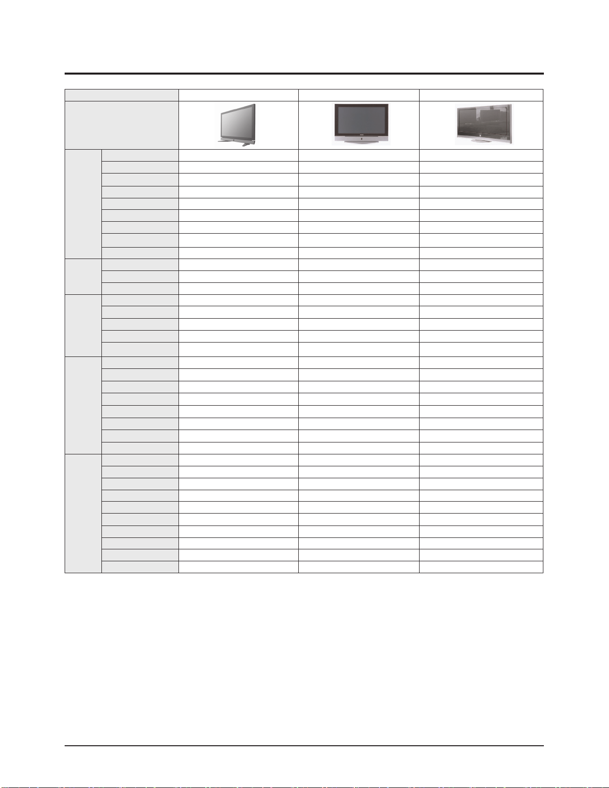
PLASMA DISPLAY TV
Chassis : D73A(P)_Twister
Model : PS42V6SX/XEH
PLASMA DISPLAY TV FEATURES
■■
DTV Ready PDP TV
■
Contrast Ratio : 10000:1
Brightness : 1500cd/m
2
■■
RF, DVI-D, PC(Analog), 2Scart,
Component, Video, S-Video
■
Slim line design
■
■
Energy Saving
SERVICE
Manual
PS-42V6S
Page 2

This Service Manual is a property of Samsung Electronics Co.,Ltd.
Any unauthorized use of Manual can be punished under applicable
International and/or domestic law.
© Samsung Electronics Co., Ltd. Sep. 2005
Printed in Korea
AA82-03063A
ELECTRONICS
Page 3

Table of Contents
Chapter 1 Precaution
■ 1-1 Safety Precautions . . . . . . . . . . . . . . . . . . . . . . . . . . . . . . . . . . . . . . . . . . . . . . . . . . . . . . . . . . . 1-1
■ 1-2 Servicing Precautions . . . . . . . . . . . . . . . . . . . . . . . . . . . . . . . . . . . . . . . . . . . . . . . . . . . . . . . . 1-3
■ 1-3 Static Electricity Precautions . . . . . . . . . . . . . . . . . . . . . . . . . . . . . . . . . . . . . . . . . . . . . . . . . . . 1-4
■ 1-4 Installation Precautions . . . . . . . . . . . . . . . . . . . . . . . . . . . . . . . . . . . . . . . . . . . . . . . . . . . . . . . 1-5
Chapter 2 Product Specification
■ 2-1 Product Features . . . . . . . . . . . . . . . . . . . . . . . . . . . . . . . . . . . . . . . . . . . . . . . . . . . . . . . . . . . . 2-1
■ 2-2 Key Features . . . . . . . . . . . . . . . . . . . . . . . . . . . . . . . . . . . . . . . . . . . . . . . . . . . . . . . . . . . . . . . 2-2
■ 2-3 Specifications Analysis . . . . . . . . . . . . . . . . . . . . . . . . . . . . . . . . . . . . . . . . . . . . . . . . . . . . . . . . 2-5
■ 2-4 Accessories . . . . . . . . . . . . . . . . . . . . . . . . . . . . . . . . . . . . . . . . . . . . . . . . . . . . . . . . . . . . . . . . 2-6
Chapter 3 Alignment & Adjustment
■ 3-1 Service Instruction . . . . . . . . . . . . . . . . . . . . . . . . . . . . . . . . . . . . . . . . . . . . . . . . . . . . . . . . . . . 3-1
■ 3-2 Factory Mode Adjustments . . . . . . . . . . . . . . . . . . . . . . . . . . . . . . . . . . . . . . . . . . . . . . . . . . . . . 3-2
■ 3-3 White Balance - Calibration . . . . . . . . . . . . . . . . . . . . . . . . . . . . . . . . . . . . . . . . . . . . . . . . . . . . 3-4
■ 3-4 Micom Update . . . . . . . . . . . . . . . . . . . . . . . . . . . . . . . . . . . . . . . . . . . . . . . . . . . . . . . . . . . . . . 3-7
■ 3-5 Replacements & Calibration . . . . . . . . . . . . . . . . . . . . . . . . . . . . . . . . . . . . . . . . . . . . . . . . . . . . 3-12
Chapter 4 Exploded View & Part List
■ 4-1 PS42V6SX/XEH . . . . . . . . . . . . . . . . . . . . . . . . . . . . . . . . . . . . . . . . . . . . . . . . . . . . . . . . . . . . . 4-1
Chapter 5 Electrical Part List
■ 5-1 PS42V6SX/XEH . . . . . . . . . . . . . . . . . . . . . . . . . . . . . . . . . . . . . . . . . . . . . . . . . . . . . . . . . . . . . 5-1
Chapter 6 Troubleshooting
■ 6-1 First Checklist for Troubleshooting . . . . . . . . . . . . . . . . . . . . . . . . . . . . . . . . . . . . . . . . . . . . . . . 6-1
■ 6-2 Checkpoints by Error Mode . . . . . . . . . . . . . . . . . . . . . . . . . . . . . . . . . . . . . . . . . . . . . . . . . . . . 6-2
■ 6-3 Trouble-shooting with New Features . . . . . . . . . . . . . . . . . . . . . . . . . . . . . . . . . . . . . . . . . . . . . 6-6
■ 6-4 Troubleshooting Procedures by ASS'Y . . . . . . . . . . . . . . . . . . . . . . . . . . . . . . . . . . . . . . . . . . . 6-9
Chapter 7 Block Diagram
■ 7-1 Overall Block Diagram . . . . . . . . . . . . . . . . . . . . . . . . . . . . . . . . . . . . . . . . . . . . . . . . . . . . . . . . 7-1
■ 7-2 Partial Block Diagram . . . . . . . . . . . . . . . . . . . . . . . . . . . . . . . . . . . . . . . . . . . . . . . . . . . . . . . . . 7-2
Page 4

Chapter 8 Wiring Diagram
■ 8-1 Overall Wiring . . . . . . . . . . . . . . . . . . . . . . . . . . . . . . . . . . . . . . . . . . . . . . . . . . . . . . . . . . . . . . . 8-1
■ 8-2 Partial Wiring . . . . . . . . . . . . . . . . . . . . . . . . . . . . . . . . . . . . . . . . . . . . . . . . . . . . . . . . . . . . . . . 8-2
Chapter 9 PCB Diagram
■ 9-1 PDP Module, SMPS . . . . . . . . . . . . . . . . . . . . . . . . . . . . . . . . . . . . . . . . . . . . . . . . . . . . . . . . . . 9-1
■ 9-2 Video Board, Function Key Borad, Power Button Board . . . . . . . . . . . . . . . . . . . . . . . . . . . . . . 9-2
Chapter 10 Schematic Diagram
■ 10-1 Main . . . . . . . . . . . . . . . . . . . . . . . . . . . . . . . . . . . . . . . . . . . . . . . . . . . . . . . . . . . . . . . . . . . . . 10-1
■ 10-2 Function . . . . . . . . . . . . . . . . . . . . . . . . . . . . . . . . . . . . . . . . . . . . . . . . . . . . . . . . . . . . . . . . . . 10-9
■ 10-3 Power/IR . . . . . . . . . . . . . . . . . . . . . . . . . . . . . . . . . . . . . . . . . . . . . . . . . . . . . . . . . . . . . . . . . 10-10
Chapter 11 Operation Instruction & Installation
■ 11-1 Product Features and Functions . . . . . . . . . . . . . . . . . . . . . . . . . . . . . . . . . . . . . . . . . . . . . . . 11-1
■ 11-2 New Features . . . . . . . . . . . . . . . . . . . . . . . . . . . . . . . . . . . . . . . . . . . . . . . . . . . . . . . . . . . . . . 11-4
■ 11-3 Installation Notes and Precautions . . . . . . . . . . . . . . . . . . . . . . . . . . . . . . . . . . . . . . . . . . . . . . 11-5
Chapter 12 Disassembly & Reassembly
■ 12-1 Overhaul Disassembly & Reassembly . . . . . . . . . . . . . . . . . . . . . . . . . . . . . . . . . . . . . . . . . . . 12-1
Chapter 13 Circuit Description
■ 13-1 Partial Block Description . . . . . . . . . . . . . . . . . . . . . . . . . . . . . . . . . . . . . . . . . . . . . . . . . . . . . 13-1
■ 13-2 New Circuit Description . . . . . . . . . . . . . . . . . . . . . . . . . . . . . . . . . . . . . . . . . . . . . . . . . . . . . . 13-25
Chapter 14 Reference Information
■ 14-1 Connection to a 3rd Party Device . . . . . . . . . . . . . . . . . . . . . . . . . . . . . . . . . . . . . . . . . . . . . . . 14-1
■ 14-2 Technical Terms . . . . . . . . . . . . . . . . . . . . . . . . . . . . . . . . . . . . . . . . . . . . . . . . . . . . . . . . . . . . 14-4
Page 5
1. Make sure all protective devices are properly installed
including non-metallic handles and compartment covers
when installing or re-installing the chassis or chassis
assemblies.
2. Make sure that no gaps exist between the cabinets for
children to insert their fingers in to prevent children from
receiving electric shocks. Gaps mentioned above include
ventilation holes of a too great magnitude between the
vaccum tube and the cabinet mask, and the improper
installation of the rear cabinet.
Errors may occur when the resistance is below 1.0 ㏁ or
over 5.2 ㏁.
In these cases, make sure that the device is repaired
before sending it back to the customer.
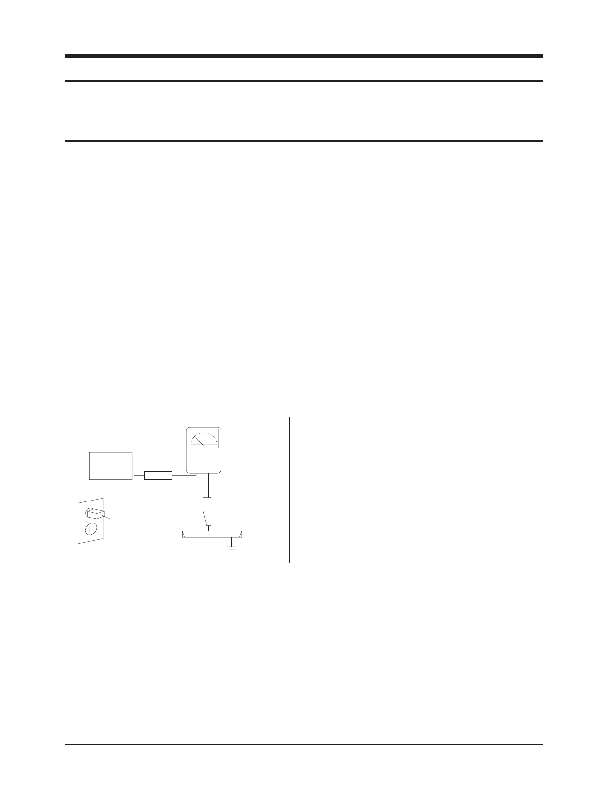
3. Check for Electricity Leakage (Figure 1-1)
Warning: Do not use an insulated transistor for checking
the leakage. Use only those current leakage testers or
mirroring systems that comply with ANSIC 101.1 and the
Underwriter Laboratory's specifications (UL1410, 59.7).
Fig. 1-1 AC Leakage Test
4. A high voltage is maintained within the specified limits
using safety parts, calibration and tolerances. When
voltage exceeds the specified limits, check each special
part.
5. Warning for Engineering Changes:
Never make any changes or additions to the circuit
design or the internal part for this product.
Ex: Do not add any audio or video accessory
connectors. This might cause physical damage.
Furthermore, any changes or additions to the original
design/engineering will invalidate the warranty.
6. Warning - Hot Chassis:
Some TV chassis are directly connected to one end of
the AC power cord for electrical reasons.
Without insulated transistors, the product can only be
repaired safely when the chassis is connected to the
earthed end of the AC power source.
To make sure the AC power cord is properly connected,
follow the instructions below. Use the voltmeter to
measure the voltage between the chassis and the
earthed ground. If the measurement is over 1.0V, unplug
the AC power cord and change the polarity before reinserting it. Measure the voltage between the chassis
and the ground again.
7. Some TV chassis are shipped with an additional
secondary grounding system. The secondary system is
adjacent to the AC power line. These two grounding
systems are separated in the circuit using an
unbreakable/unchangeable insulation material.
8. When any parts, material or wiring appear overheated or
damaged, replace them with new regular ones
immediately. When any damage or overheating is
detected, correct this immediately and make a regular
check of possible errors.
9. Check for the original shape of the lead, especially that
of the antenna wiring, any sharp edges, the AC power
and the high voltage power. Carefully check if the wiring
is too tight, incorrectly placed or loose. Never change the
space between the part and the printed circuit board.
Check the AC power cord for possible damages. Keep
the part or the lead away from any heat-emitting
materials.
Precaution
Samsung Electronics 1-1
To avoid possible damages or electric shocks or exposure to radiation, follow the instructions below with regard to safety,
installation, service and ESD..
1. Precaution
1-1 Safety Precautions
(READING SHOULD
DEVICE
UNDER
TEST
EXPOSED METAL
2-WIRE CORD
ALSO TEST WITH
PLUG REVERSED
(USING AC ADAPTER
PLUG AS REQUIRED)
TEST ALL
SURFACES
LEAKAGE
CURRENT
TESTER
NOT BE ABOVE
0.5mA)
EARTH
GROUND
Page 6

10. Safety Indication:
Some electrical circuits or device related materials
require special attention to their safety features, which
cannot be viewed by the naked eye. If an original part is
replaced with another irregular one, the safety or
protective features will be lost even if the new one has a
higher voltage or more watts.
Critical safety parts should be bracketed with ( ).
Use only regular parts for replacements (in particular,
flame resistance and dielectric strength specifications).
Irregular parts or materials may cause electric shock or
fire.
11. Pay additional attention to the current leakage as the
voltage between the power board and the ballast is 220
to 440v, i.e. very high.
And also beware of possible electric shock from the
primary power source.
Precaution
1-2 Samsung Electronics
!
Page 7

1. The service instructions are printed on the cabinet, and
should be followed by any service personnel.
2. Make sure to unplug the AC power cord from the power
source before starting any repairs.
(a) Remove or re-install parts or assemblies.
(b) Disconnect the electric plug or connector, if any.
(c) Connect the test part in parallel with the electrolytic
capacitor.
3. Some parts are placed at a higher position than the
printed board. Insulated tubes or tapes are used for this
purpose. The internal wiring is clamped using buckles to
avoid contact with heat emitting parts. These parts are
installed back to their original position.
4. After the repair, make sure to check if the screws, parts
or cables are properly installed. Make sure no damage is
caused to the repaired part and its surroundings.
5. Check for insulation between the blade of the AC plug
and that of any conductive materials (i.e. the metal
panel, input terminal, earphone jack, etc).
6. Insulation Check Process: Unplug the power cord from
the AC source and turn the switch on. Connect the insulating resistance meter (500v) to the AC plug blade.
The insulating resistance between the blade of the AC
plug and that of the conductive material should be more
than 1 ㏁.
7. Any B+ interlock should not be damaged.
If the metal heat sink is not properly installed, no
connection to the AC power should be made.
8. Make sure the grounding lead of the tester is connected
to the chassis ground before connecting to the positive
lead. The ground lead of the tester should be removed
last.
9. Beware of risks of any current leakage coming into
contact with the high-capacity capacitor.
10. The sharp edges of the metal material may cause
physical damage, so ensure wearing protective gloves
during the repair.
11. Due to the nature of plasma display panels, partial afterimages may appear if a still picture is displayed on the
screen for a long period of time.
This is caused by brightness deterioration due to the
storage effect of the panel, and to prevent this from
happening, we recommend that the brightness and contrast are reduced.
(e.g.) Contrast: 25, Brightness: 50
12. A plasma panel is a device which consists of a set of
clustered pixels (cells).
A plasma panel is approved if over 99.9% of the
components satisfy the necessary conditions. A few cells
may stay illuminated or may be always off, but you do
not have to worry as this is an approved panel and well
within the standard.
Precaution
Samsung Electronics 1-3
Warning 1: First carefully read the "Safety Instruction" in this service manual.
When there is a conflict between the service and the safety instructions, follow the safety instruction at all times.
Warning 2: Any electrolytic capacitor with the wrong polarity will explode.
1-2 Servicing Precautions
Page 8

1-3 Static Electricity Precautions
1. Some semi-conductive ("solid state") devices are
vulnerable to static electricity. These devices are known
as ESD. ESD includes the integrated circuit and the field
effect transistor. To avoid any materials damage from
electrostatic shock, follow the instructions described
below.
2. Remove any static electricity from your body by
connecting the earth ground before handling any
semi-conductive parts or ass'ys. Alternatively, wear a
dischargeable wrist-belt.
(Make sure to remove any static electricity before
connecting the power source - this is a safety instruction
for avoiding electric shock)
3. Remove the ESD ass'y and place it on a conductive
surface such as aluminum foil to prevent accumulating
static electricity.
4. Do not use any Freon-based chemicals.
Such chemicals will generate static electricity that
causes damage to the ESD.
5. Use only grounded-tip irons for soldering purposes.
6. Use only anti-static solder removal devices.
Most solder removal devices do not support an
anti-static feature. A solder removal device without an
anti-static feature can store enough static electricity to
cause damage to the ESD.
7. Do not remove the ESD from the protective box until the
replacement is ready. Most ESD replacements are
covered with lead, which will cause a short to the entire
unit due to the conductive foam, aluminum foil or other
conductive materials.
8. Remove the protective material from the ESD
replacement lead immediately after connecting it to the
chassis or circuit ass'y.
9. Take extreme caution in handling any uncovered ESD
replacements. Actions such as brushing clothes or lifting
your leg from the carpet floor can generate enough static
electricity to damage the ESD.
Precaution
1-4 Samsung Electronics
CAUTION
These servicing instructions are for use by
qualified service personnel only.
To reduce the risk of electric shock do not
perform any servicing other than that contained in the
operating instructions unless you are qualified to do so.
Page 9

Precaution
Samsung Electronics 1-5
1-4 Installation Precautions
1. For safety reasons, more than two people are required
for carrying the product.
2. Keep the power cord away from any heat emitting
devices, as a melted covering may cause fire or electric
shock.
3. Do not place the product in areas with poor ventilation
such as a bookshelf or closet. The increased internal
temperature may cause fire.
4. Bend the external antenna cable when connecting it to
the product. This is a measure to protect it from being
exposed to moisture. Otherwise, it may cause a fire or
electric shock.
5. Make sure to turn the power off and unplug the power
cord from the outlet before removing the product. Also
check the antenna cable or the external connectors if
they are fully unplugged. Damage to the cord may cause
fire or electric shock.
6. Keep the antenna far away from any high-voltage cables
and install it firmly. Contacting the high-voltage cable or
the antenna falling over may cause fire or electric shock.
7. When connecting the RF antenna, check for a DTV
receiving system and install a separate DTV reception
antenna for areas with no DTV signal.
8. When installing the product, leave enough space (10cm)
between the product and the wall for ventilation
purposes.
A rise in temperature within the product may cause fire.
9. When moving a PDP with attached speakers, detach the
speakers first before moving the main body.
Moving the PDP main body without separating the
speakers may cause the speakers to detach, possibly
causing damage or injury.
Page 10

1-6 Samsung Electronics
MEMO
Page 11
Product Specification
Samsung Electronics 2-1
2. Product Specification
2-1 Product Features
■ Chip Description
- FLI5921H(IC310) : Scaler, On-chip MCU + Serial FLASH ROM, Dual Analog RGB and YUV Input
DVI + HDCP, Flexible PIP support
- VCT49x7F(IC210) : CVBS, Y/C Sub Video signal , Scart RGB signal processing,
TV-sound demodulation, Baseband sound processing for loudspeaker channel
Multi-standard QSS IF processing with single SAW
multi-standard color decoder (PAL/NTSC/SECAM)
4H adaptive comb filter (PAL/NTSC)
- TPA3008D(IC611) : Audio power amplifierS
Block Specfication Major IC Remark
RF Tuner TECH0849PG46A SEMCO
Power Input Voltage : AC 220 - 240 V~, 50 Hz
Video
Scaler FLI5921H(CPU & Scaler) GENESIS
Video Decoder VCT49x7F MICRONAS
Sound
Sound Processor VCT49x7F MICRONAS
Sound AMP TPA3008 Texas Instruments
Audio S/W 74HC4052
PDP Module Samsung SDI V4 42" SD SAMSUNG SDI
Remocon TM79
Cabinet V6
Page 12
Product Specification
2-2 Samsung Electronics
2-2 Key Features
Model PS-42V6S
Dimensions 1425(W) x 114(D) x 825.4(H) mm
Weight 40 Kg
Voltage EU : AC 220-240V~, 50Hz / CIS : AC 100-240V~, 50/60Hz
Power Consumption 290 W
Number of Pixels 852 (H) x 480 (V)
Screen Size 42 inches
VIDEO input
TV (VHF, UHF Antenna)
Scart1(AV)
Scart2(AV, RGB)
CVBS/S-Video
COMPONENT(480i/480p/720p/1080i)
PC
DVI
AUDIO input
Scart1
Scart2
Component
PC
DVI
Audio Output
8W + 8W ( 8Ω )
■ H/W Configuration
- Video : VCT49x7F, FLI5921
- Sound : VCT49x7F, TDA3008D
- Tuner : TECH0849PG46A
■ S/W Configuration
- CPU + Scaler : FLI5921(Genesis)
- Video Decoder : VCT49X7F(Micronas)
■ Picture
- Video System : PAL/SECAM/NTSC4.43
- Progressive scan
- Output resolution : 852(H) x 480(V)
- Still picture, Noise reduction
- Comb Filter : 4H comb filter(VCT49X7F integrated)
- Mode : Dynamic, Standard, Movie, Custom
- PIP(Size : Large)
Page 13

Product Specification
Samsung Electronics 2-3
■ Sound
- System : Stereo
- Output : 8W + 8W
- Speaker : built-in
■ Feature
- Component Interface(480i/480p/720p/1080i, Y/Pb/Pr)
- Digital Interface : DVI
- Picture Size : Auto Wide/16:9/4:3/Panorama/14:9/Zoom/Wide 4:3
- Auto Store
- Sleep Timer : 180 minute
- Clock
- Zoom, Previous channel, Blue Screen, Color Tone, Screen Burn Protection
■ In/Out Terminals(Rear)
- 1 AV Input, 1 SVHS Input
- Component Input : 480i / 480p / 720p / 1080i
- 15 Pin D-sub Input : ~ XGA (1024 x 768)
- DVI input : DTV(480p / 720p / 1080i)
- 1 RF Input
■ Remocon
- TM79
■ Power Supply
- EU : AC 220-240V, 50Hz
- CIS : AC 100-240V~, 50/60Hz
■ Power
- Max Power : 290 W
Page 14
Product Specification
2-4 Samsung Electronics
■ The table below shows all of the display modes that are supported. (N : Negative, P : Positive)
Resolution V-Freq.(Hz) H-Freq.(kHz)
Polarity
H V
IBM PC/AT
Compatible
640 X 350 70.086 31.469 N P IBM
720 X 400 70.087 31.469 P N IBM
640 X 480
59.940 31.469 N N VESA DMT
70.000 35.000 N/P N/P VESA GTF
72.809 37.861 N N VESA DMT
75.000 37.500 N N VESA DMT
800 X 600
56.250 35.156 N/P N/P VESA DMT
60.317 37.879 P P VESA DMT
70.000 43.750 N/P N/P VESA GTF
72.188 48.077 P P VESA DMT
75.000 46.875 P P VESA DMT
848 X 480
60.000 31.020 P P VESA DMT
74.769 37.684 N P VESA CVT
1024 X 768
60.004 48.363 N N VESA DMT
70.069 56.476 N N VESA DMT
72.000 57.672 N/P N/P VESA GTF
75.029 60.023 P P VESA DMT
▶ The interlace mode is not supported.
▶ The television might operate abnormally if a non-standard video format is selected.
▶ 480i/p, 576i/p, 720p, or 1080i is not available in pc mode.
Page 15
Product Specification
Samsung Electronics 2-5
2-3 Specifications Analysis
Model Twister(V4) Puccini(V4) Mozart (V3)
Design
Basic
Display Type PDP TV PDP TV PDP TV
Built-In Tuner O O O
Resolution
852 X 480 852 X 480 852 X 480
PDP Module V4 V4 V3
Screen Size 42 inches 42 inches 42 inches
Aspect Ratio 16 : 9 16 : 9 16 : 9
Power Consumption 290 W 290 W 330 W
Dimensions 14255(W) x 114(D) x 825.4(H) mm 14255(W) x 114(D) x 825.4(H) mm 14255(W) x 114(D) x 825.4(H) mm
Weight 40 Kg 59.2 Kg 59.2Kg
Picture
Brightness 1,500 Cd/m2 1,500 Cd/m2 1,000 Cd/m2
Contrast Ratio 10,000 : 1 10,000 : 1 3,000 : 1
Image Enhacer X DNIe-L DNIe 3
Audio
Equalizer O O O
Auto Volume O O O
Surround Sound X SRS TruSurround SRS TreSurround XT
Speaker Output 8 W + 8 W 15 W + 15 W 15 W + 15 W
Speaker Included Included Included
Features
PIP O O O
Double Screen O O O
TTX O O O
Still Image O O O
My Color Control X O O
Color Weakness X O O
Energy Saving O O X
Screen Burn Protection O O O
Connections
Antenna 1 Input 1Input 1Input
CVBS 1 AV 1AV 3 AV
S-Video 1 Input 1 Input 2 Input
Component(Y/PB/PR) 1 Input 1 Input 1 Input
PC(D-SUB) 1 Input 1 Input 1 Input
DVI 1 Input X 1 Input
HDMI X 1 Input X
Sub Woofer X X X
Optical X X X
Coaxial X X X
Page 16
Product Specification
2-6 Samsung Electronics
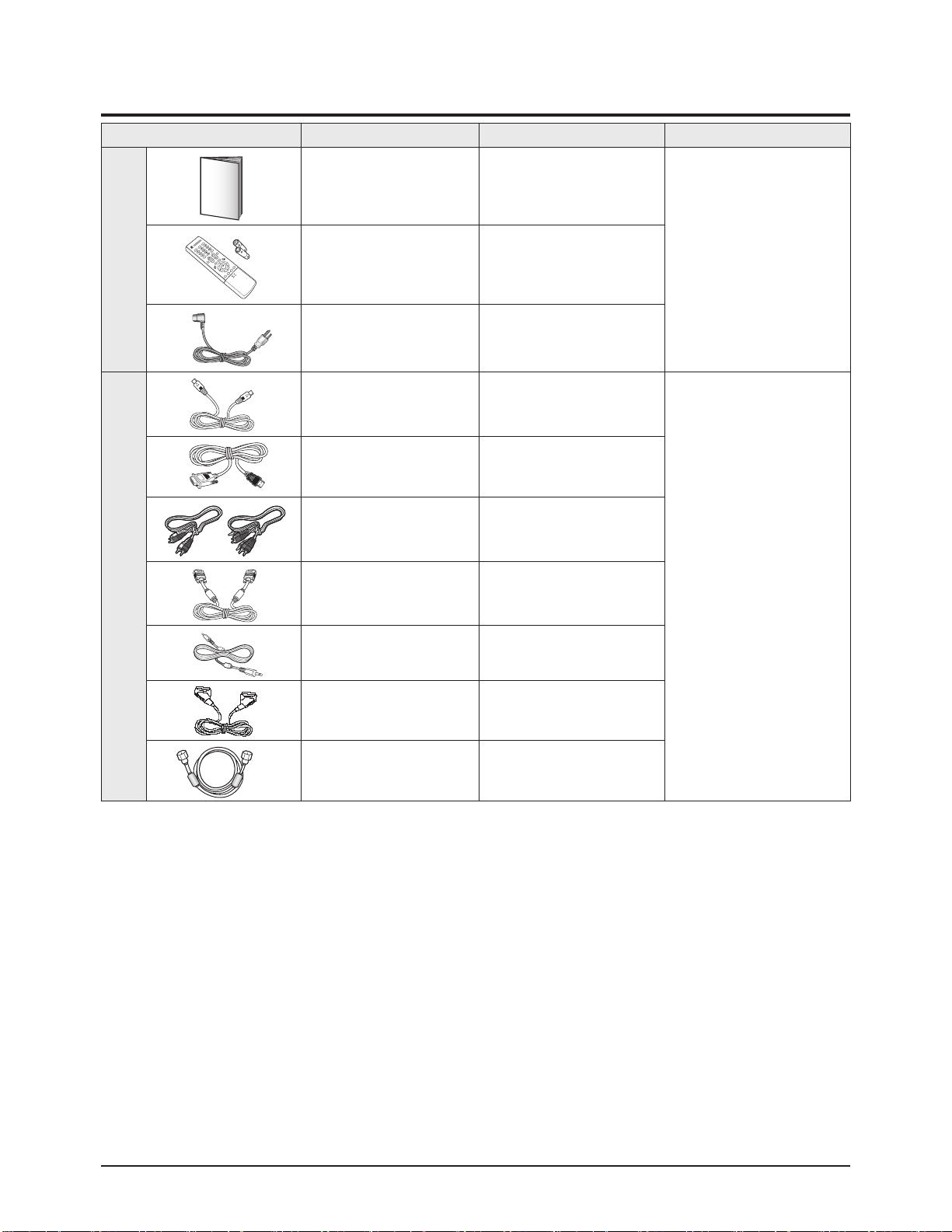
2-4 Accessories
Accessories Item Item code Remark
Supplied Accessories
User Manual BN68-00955A
Samsung Service center
Remote Control
AAA Batteries
BN59-00488A
4301-000103
Power Cord 3903-000145
Accessories that can be purchased
additionally
S-VIDEO Cable -
Internal shopping mall
HDMI/DVI cable -
Component Cables (RCA) -
PC Cable -
PC Audio Cable -
Scart Cable -
Antenna Cable -
Page 17

Alignment & Adjustment
Samsung Electronics 3-1
3. Alignment & Adjustment
3-1 Service Instruction
* Check items listed after changing each
1. Main Board replace : ATM Channel fixing and White Balance adjustment
2. Main SMPS Board replace: Vs, Va Voltage check and adjust
5. DC-DC SMPS Board replace : Output voltage check and adjust
6. Logic Board replace : Not adjustment
7 : Y-Main Board replace : Not adjustment
8 : X-Main Board replace : Not adjustment
9 : Buffer Board replace : Not adjustment
Page 18
Alignment & Adjustment
3-2 Samsung Electronics
3-2 Factory Mode Adjustments
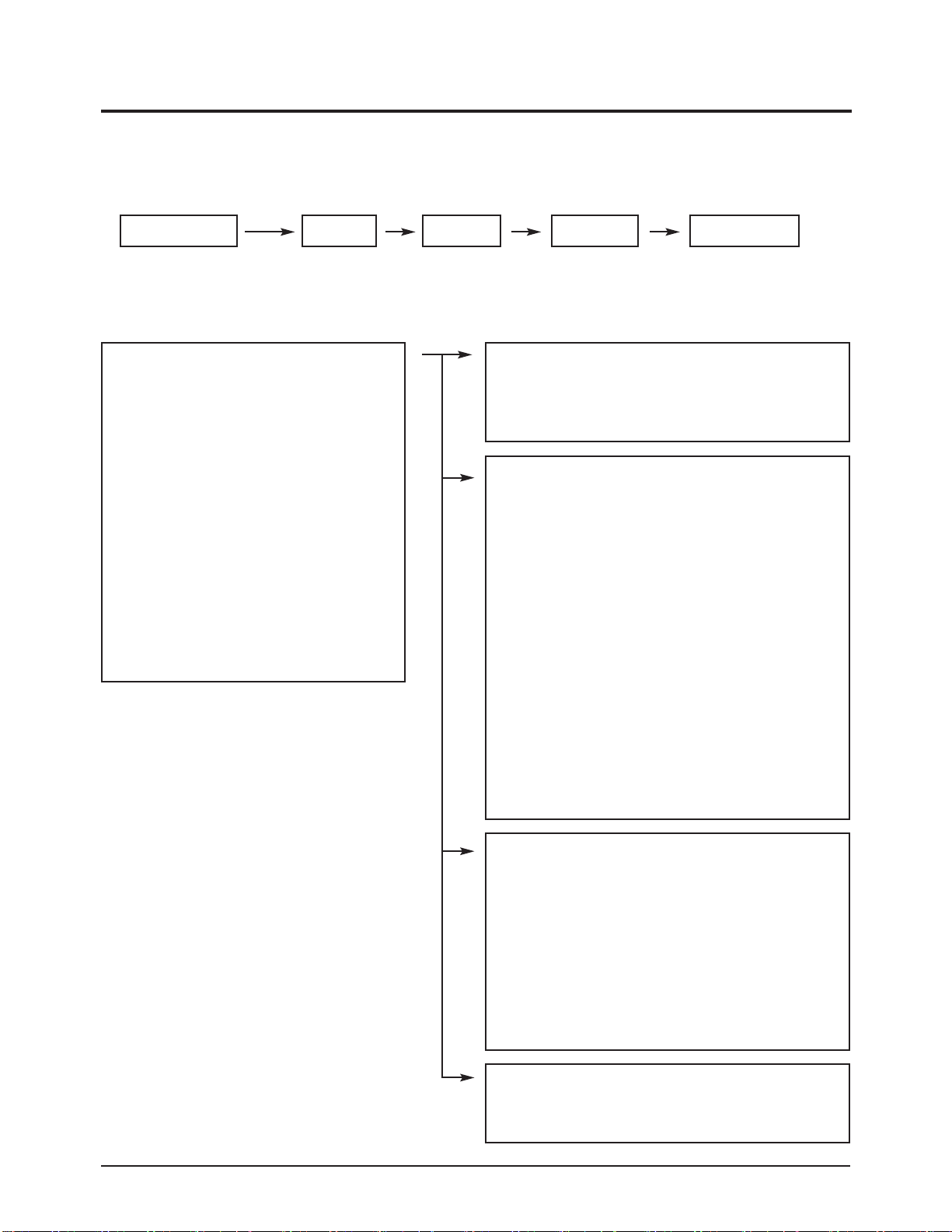
3-2-1 Entering Factory Mode
To enter 'Service Mode' Press the remote -control keys in this sequence :
- If you do not have Factory remote - control
3-2-2 Factory Mode Tree
- If you have Factory remote - control
[INFO] →→[FACTORY]
Power OFF MENU MUTE Power OnINFO
1. Calibration
2. Option Byte
3. W/B
4. VCTi
5. YC Delay
6. FLI5961
7. Adjust
8. Test Pattern
9. Password
10. Check Sum
11. Spread Spectrum
12. HDCP
13. Download
14. Reset
T-TWS42PEUS-XXXX
P-TRNPEU-XXXX
Firmware Version
1. Calibration : W/B Calibration
AV Calibration
DTV Calibration
PC Calibration
2. Option byte : Setting option
Panel option : 42" PDP
Gamma
:
off/on
Auto Power : on/off
Video Mute : 5
Language : English
Hotel Mode : off/on
LNA Plus : off/on
V-chip : off
Auto FM : off/on
High Deviation : off/on
TTX List : Flop/List
TTX Top : off/on
TTX Group :
User OSD/West Europe/East Europe/
Russian/Greek
· Turkey/Arabic/
Farisian/Arab.Habrew/Off
DVI : on/off
- - - - :
3. W/B : Adjustment White Balance
( Range 0~255 )
Sub Bright : 128
R off set : 128
G off set : 128
B off set : 128
Sub contrast : 128
R gain : 128
G gain : 128
B gain : 128
4.
VCTi
:
VCTi IC Correct register
VCTi Page 1
VCTi Page 2
Page 19
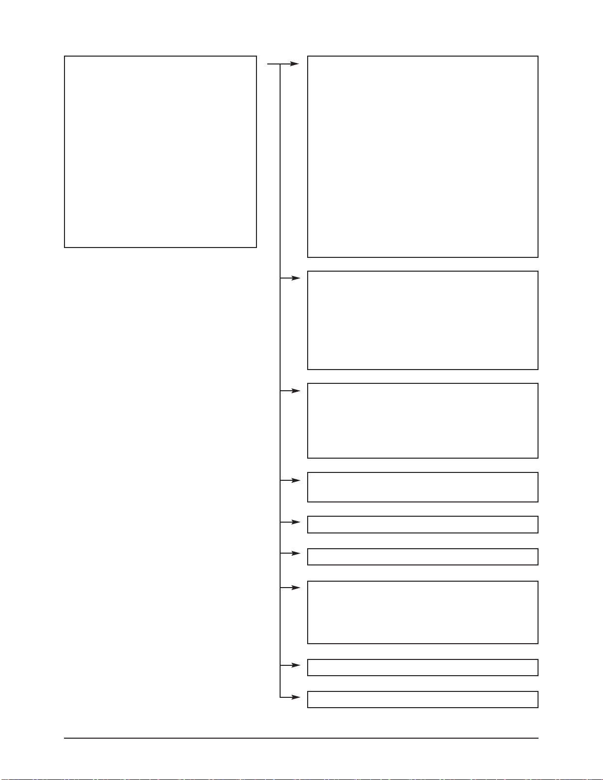
Alignment & Adjustment
Samsung Electronics 3-3
1. Calibration
2. Option Byte
3. W/B
4. VCTi
5. YC Delay
6. FLI5961
7. Adjust
8. Test Pattern
9. Chip Debugger
10. Check Sum
11. Spread Spectrum
12. HDCP
13. Reset
T-TRNPEU-0000 month day year time
P-TRNPEU-0000
Panel On Time(Hour) 0000
5. YC Delay
RF PAL-B/G : 5
RF PAL-D/K : 6
RF PAL-I : 5
RF PAL-L/L' : 7
RF SECAM-B/G : 2
RF SECAM-D/K : 0
RF SECAM-I : 2
RF SECAM-L/L' : 6
RF NTSC 3.58 : 5
RF NTSC 4.43 : 5
AV PA L : 5
AV SECAM : 7
AV NTSC 3.58 : 5
AV NTSC 4.43 : 5
AV PAL 60 : 5
6. FLI5961 : Scaler IC Correct register
Component Calibration
: Result DTV Calibration
PC Calibration : Result PC Calibration
ACC/ACM
TNR
Picture Enhance
User W/B
7. Adjust
User Control lnitial
LNA PLUS
Hotel Option
Pixel Shift
11. Spread Spectrum
Spread Spectrum
: on/off
Spread Spectrum Range
: 2
Step : 63
8. Test Pattern : VCTi IC'S own test patterns.
(Total 7 patterns)
10. Check Sum : 0000
12. HDCP : 0000
13. Download : Off/On
9. Password : Use IC Register Correction.
Page 20
Alignment & Adjustment
3-4 Samsung Electronics
3-3 White Balance - Calibration
3-3-2 White Balance - Adjustment
3-3-1 White Balance -Calibration
3-3-3 Conditions for Measurement
1. Calibration
DTV Calibration
PC Calibration
(Calibration Condition refer to next page)
3. W/B
(low light) (hight light)
1. On the basis of toshiba ABL pattern : High Light level (57 IRE)
- INPUT SIGNAL GENERATOR : MSPG-925LTH
* Mode NO 1 : 744X484@60 Hz
NO 6 : 1280X720@60 Hz (Component 720P)
NO 21 : 1024X768@60 Hz
*
Pattern
NO 15 : Color bar
NO 16 : Toshiba ABL Pattern
NO 17 : 16 gray
2. Optical measuring device : CA210 (FL)
Please use the MSPG-925 LTH generator for model LNR2355W,LNR2755W,LNR3255W.
(W/B adjustment Condition refer next page)
Sub Bright Sub Contrast
R offset R gain
G offset G gain
B offset B gain
Page 21
Alignment & Adjustment
Samsung Electronics 3-5
2. Adjust the white balance of AV, Component and DVI Modes.
a) Set the input to the mode in which the adjustment will be made (AV Component DVI).
* Input signal - VIDEO Mode : Model #1 (744X484 Mode), Pattern #16
- Component, DVI Mode : Model #6 (1280X720 Mode), Pattern #16
b) Enter factory W/B.
c) Adjust the low light.
- Adjust sub - Brightness to set the 'Y' value.
- Adjust red offset ('x') and blue offset ('y') to the color coordinates. ( x : 280, y : 285, Y : 1.1fL)
* Do not adjust green offset data.
3-3-4 Method of Adjustment
1. Adjust the basic level of Component and PC input signals.
a) Set the input to the mode in which the adjustment will be made (Component PC ).
* Input signal - Component Mode : Model #6 (1280X720 Mode), Pattern #15 (picture 4-1)
- PC Mode : Model #21 (1024X768 Mode), Pattern #17 (Picture 4-2)
b) Enter factory Calibration (DTV, PC Mode Only).
* DTV Calibration Source change for PC PC Calibration
Picture 4-1 Color bar
Picture 4-2 16gray
Picture 4-3 Toshiba ABL Pattern
Low light
Measurement point
Page 22
Alignment & Adjustment
3-6 Samsung Electronics
Picture 4-4 Toshiba ABL Pattern
High light
Measurement point
d) Adjust the high light. (Refer to table 1, 2 in adjustment position by mode)
- Adjust red gain ('x') and blue gain ('y') to the color coordinates. ( x : 265, y : 265 )
* Do not adjust the green gain and sub-contrast (Y) data.
Page 23
Alignment & Adjustment
Samsung Electronics 3-7
3-4 Micom Update
3-4-1 Installing G-Probe
1. Uncompress GProbe5.1.0.18.zip.
2. Run GProbe5.1.0.18.exe.
3. The files are created in the C:₩Program Files₩Genesis Microchip₩GProbe 5 folder.
4. Copy the ispoak_spi.hex file to the C:₩Program Files₩Genesis Microchip₩GProbe 5 folder.
5. Uncompress FLI5961-AC_GProbe_S0006-CSC-33B.zip.
6. Three files are extracted (FLI5961.Chip.GProbe, FLI5961.chm, outputlog.txt).
7. Copy all 3 files to the C:₩Program Files₩Genesis Microchip₩GProbe 5₩ChipDB folder.
8. Run GProbe.exe in the C:₩Program Files₩Genesis Microchip₩GProbe 5 folder. The G-Probe program is created.
<The screen that appears when G-Probe is successfully installed>
Page 24
Alignment & Adjustment
3-8 Samsung Electronics
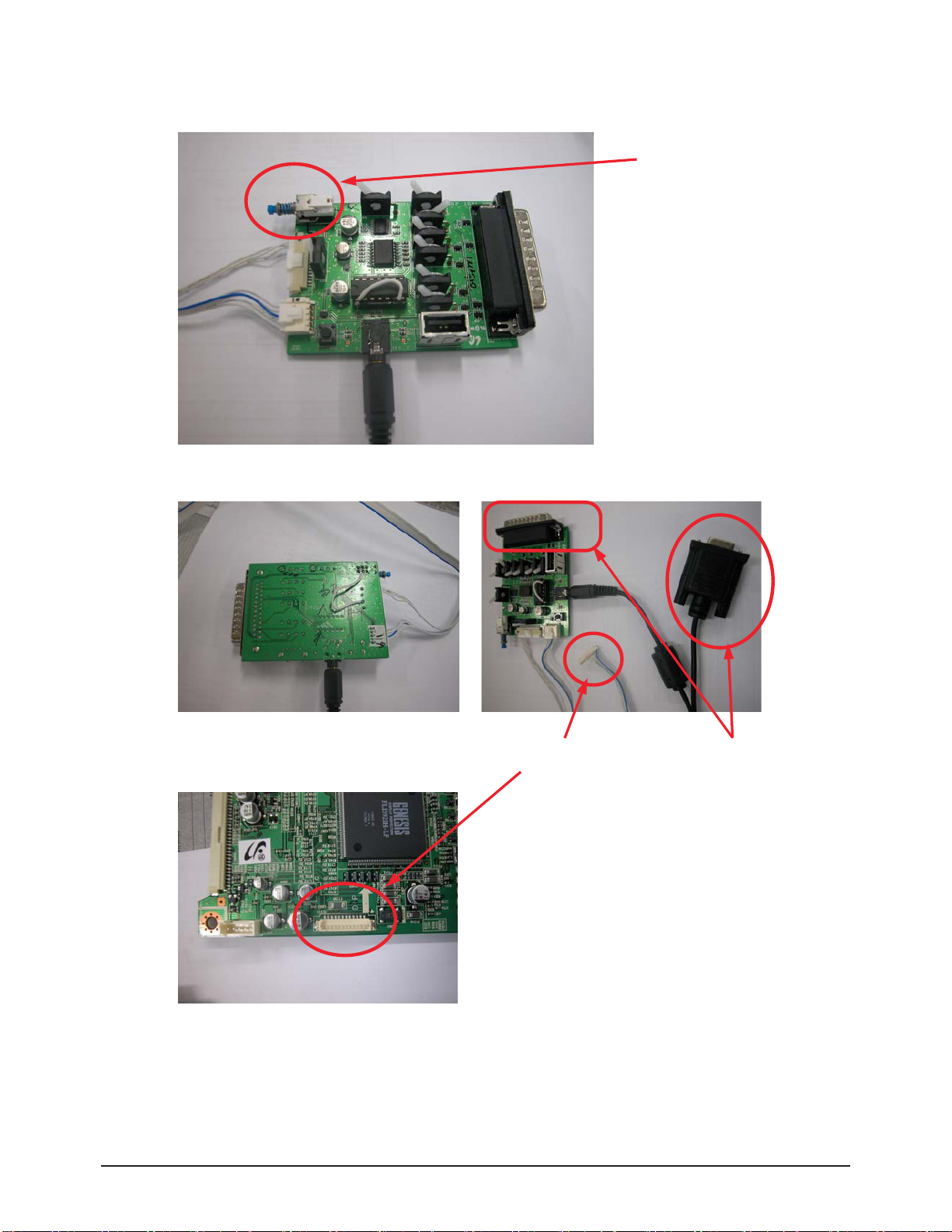
3-4-2 Connecting to the MAIN PCB
Switch off
<Bottom Side>
Connect to the PC
Connect to the MAIN PCB.
<Micom Download Jig Top Side: Note the direction of the switch>
Page 25

Alignment & Adjustment
Samsung Electronics 3-9
3-4-3 Update Procedures
1. Open twister.txt in the C:₩Program Files₩Genesis Microchip₩GProbe 5 folder.
2. The following result will appear.
//
// Batch file to program a sPI serial flash using ISP.
// Moving the stack to high memory area is now taken care of in IROM
// through the "Reset 0" command. Assumes the ISP driver is in the same
// directory as this file. Change ISP driver path in "fastFlashWrite"
// command, if different from current directory.
//
debugon
SetBuffer 0x2000 0x800
delay 200
Reset 0
delay 500
// SPI flash driver
RAMWrite ispoak_spi.hex
Run 0x500
delay 100
// Optional - Get Flash ID. The second parameter is a don't care
//FLASHCRC 0xff0000 0x20000
// Command delay for flash erase
SetDelay 1000 9000
FlashErase
// Command delay for flash write. This is for each flash write packet (upto 4 k Bytes)
SetDelay 1000 3000
// Change this line to point to a file in a different location, if needed
//fastFlashWrite C:₩Proj₩OAK₩APP-59xx₩debug₩obj₩59xx_proj.hex
fastFlashWrite C:₩C:₩Program Files₩Genesis Microchip₩GProbe 5₩T_TWSPEU.hex
// Optional - Get CRC of 128 kByte flash. For other sizes, change second parameter
// accordingly
//FLASHCRC 0x80000 0x20000
// to reset the monitor after programming the flash using DDC2BI ONLY:
// Un-comment the following three lines (PLEASE - FOR DDC2BI PORT SELECTED ONLY)
//0x8000=1
//0x8003=0
//0x8027=1
Page 26
Alignment & Adjustment
3-10 Samsung Electronics
The Micom program is to be copied to the folder marked in red and the name of the program is to be the same as the file name
marked in blue.
(If the Micom program is not in the folder marked in red, change the path to the folder which includes the Micom program and
then save the file.)
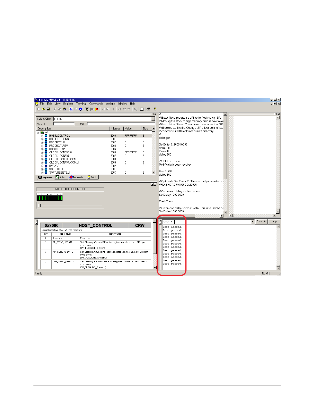
3. When completing all the procedures above, connect the Jig and the PCB, and run the G-Probe program.
After that Enter 'test 10' as shown in the following figure and press Enter or click the Execute button.
If the result appears as shown in the following figure, it is properly connected.
Page 27
Alignment & Adjustment
Samsung Electronics 3-11
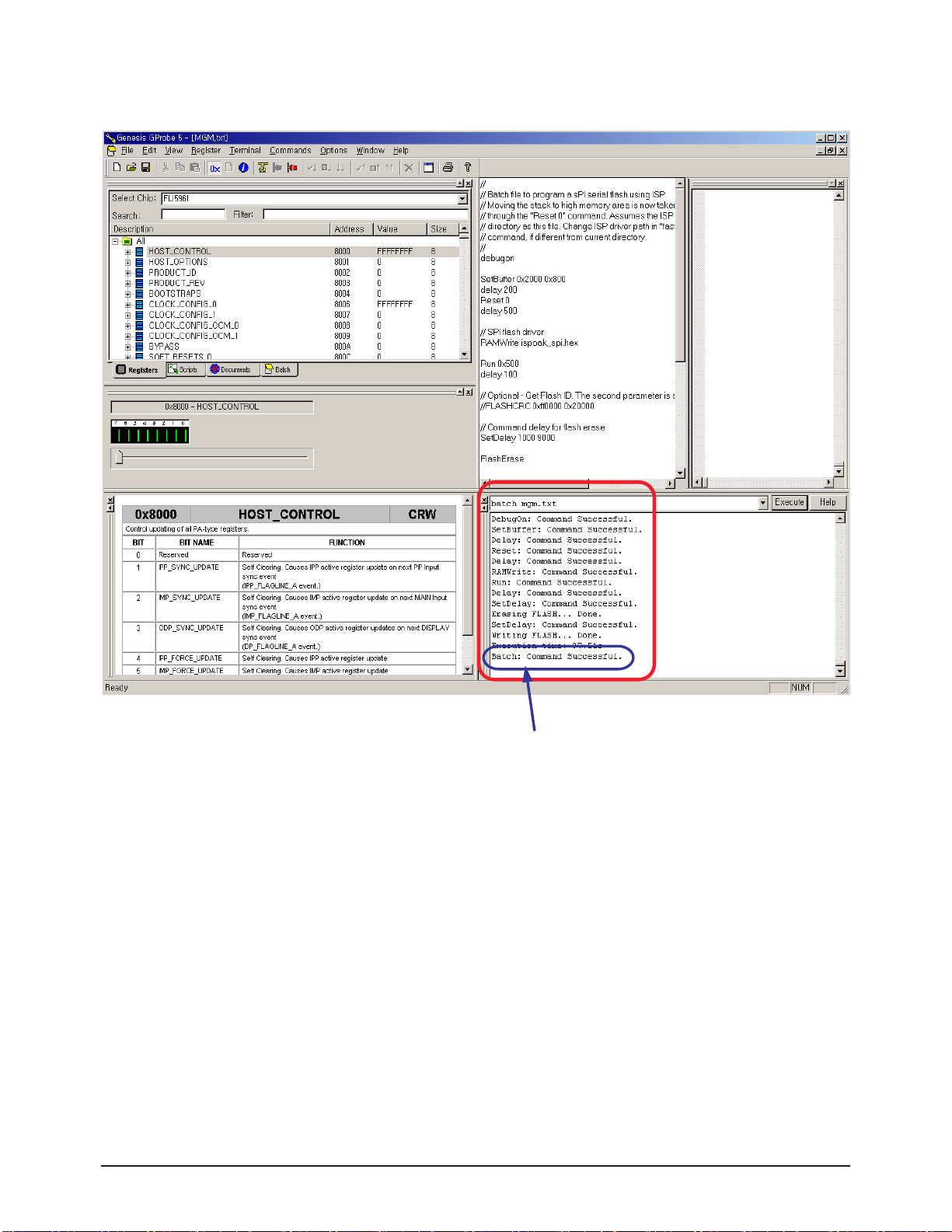
4. Enter "batch twister.txt" as show in the following figure and press Enter or click the Execute button to update Micom.
If the MICOM update is successfully completed, the above
message appears.
Page 28
Alignment & Adjustment
3-12 Samsung Electronics
3-5 Replacements & Calibration
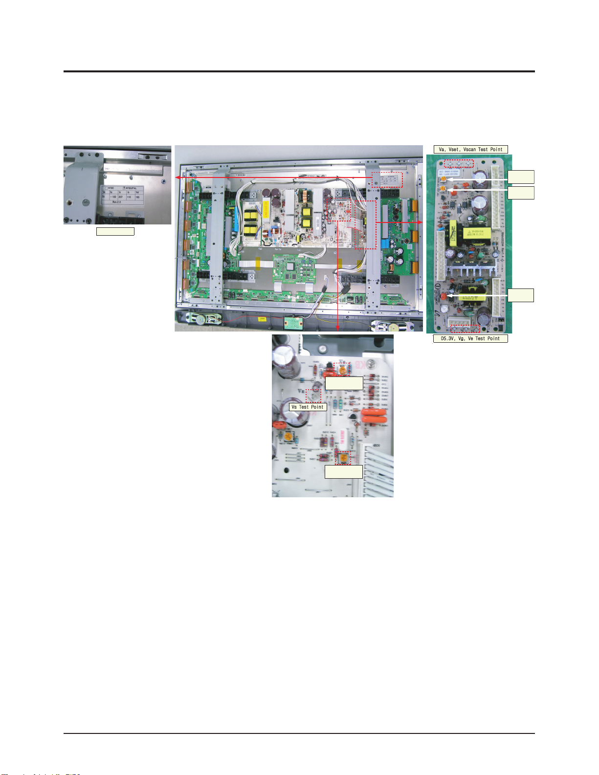
3-5-1 Voltage Adjustment
※ When the SMPS is replaced, the Va, Vs voltages must be checked and adjusted to the proper levels indicated on the panel
sticker.
adjustment
adjustment
Voltage Label
adjustment
Vscan
Vset
Ve
VRU801 VS
adjustment
VRA801 Va
adjustment
Page 29
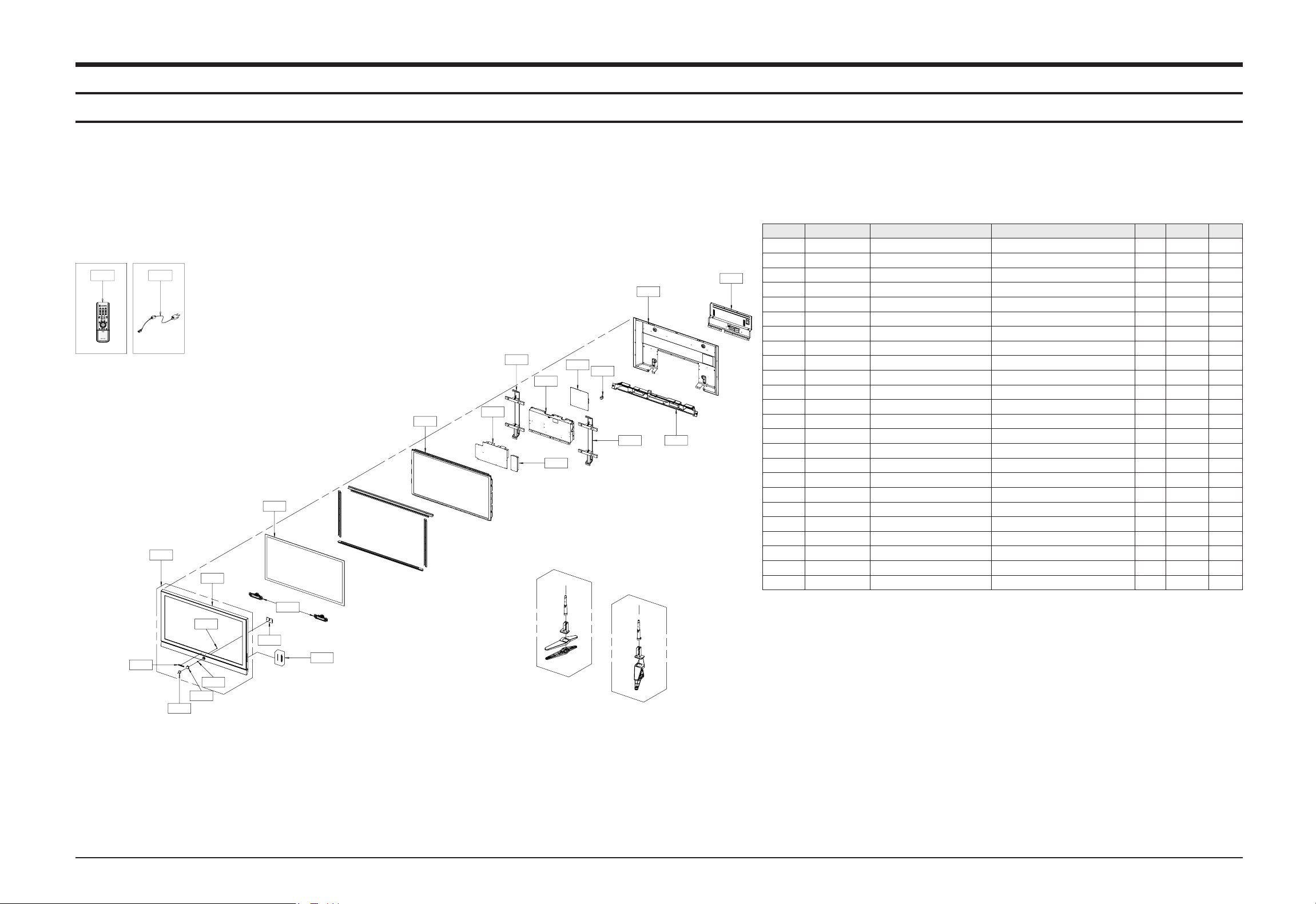
4. Exploded View & Part List
Exploded View & Part List
Samsung Electronics 4-1
You can search for the updated part code through ITSELF web site.
URL:http://itself.sec.samsung.co.kr
4-1 PS42V6SX/XEH
Loc.No. Code No. Description Specification Q'ty SA/SNA Remark
FT532 2901-001357 FILTER-EMI AC LINE 250V,6A,UL/SA/VDE,0.1 1 S.A
M0013 BN96-02743A ASSY COVER P-REAR 42V6,PCM T0.5 1 S.A
M0013 BN96-02744A ASSY COVER P-REAR BOTTOM 42V6,HIPS HB,BK 1 S.A
M0112 BN63-02216A COVER-FRONT 42V6,HIPS,HB,XEC,BLK(BK500), 1 S.N.A
M0145 BN96-02784A ASSY BOARD P-FUNCTION TWISTER,CT5000-385 1 S.A
M0146 BN96-02050D ASSY BOARD P-POWER & IR Twister,CT5000-3 1 S.A
T0003 BN96-02737A ASSY COVER P-FRONT 42V6,XEC,HIPS HB,BLK( 1 S.A
T0023 BN64-00419A KNOB-POWER 42V6,PC,VIOLET 1 S.N.A
T0023 BN64-00421A KNOB POWER 42V6,DECO,ABS,HB,BLK(BK500),C 1 S.N.A
T0044 BN96-01887A ASSY PDP MODULE P M1,PS42S5S,D,V4,1002¡¿ 1 S.A
T0054 BN64-00122A SCREEN-EMI,FILTER FILTER,42P3,984*584,T3 1 S.A
T0057 BP64-00177A BADGE-BRAND ALL,AL,T1.5,70,11.3,BLK,SILI 1 S.N.A
T0060 BN61-02184A SPRING ETC SUS304,OD11.2,L23,N7 1 S.A
T0071 BN64-00366A INDICATOR-LED ROME-I,PC,CLEAR,ALL MODEL 1 S.N.A
T0074 BN59-00488A REMOCON TORINO-EO,TM79,Single Micom,39,E 1 S.A
T0079 BN94-00759A ASSY PCB MISC-MAIN BN41-00649A,TWISTER 1 S.A
T0098 BN96-02780A ASSY PCB P PS-42V6S,80*190mm,reactor 1 S.A
T0152 BN96-01774A ASSY BRACKET P-WALL RIGHT SPD-42P5HD,SEC 1 S.N.A
T0159 BN96-02413B ASSY PCB P-SMPS PS-42V6S,220V(only),370* 1 S.A
T0175 BN96-02785A ASSY SPEAKER P 8ohm,Twister,42inch,10W 1 S.A
T0268 3903-000145 CBF-POWER CORD DT,EU,FP3/YES,U(IEC C13-R 1 S.A
T0312 BN96-02135E ASSY COVER P-REAR SUB 42V6,SECC,T1.0,TWI 1 S.N.A
T0448 BN96-01775A ASSY BRACKET P-WALL LEFT SPD-42P5HD,SECC 1 S.N.A
T0448 BN96-02742A ASSY BRACKET P-TERMINAL 42V6,XEC,SECC T0 1 S.N.A
T0074
T0268
T0054
T0003
M0112
T0044
T0159
T0152
T0312
T0098
T0079
FT532
T0448
M0013
M0013
T0448
T0175
T0071
M0146
T0057
T0060
T0023
T0023
M0145
Page 30
Electrical Part List
5. Electrical Part List
5-1 PS42V6SX/XEH Service Item
You can search for the updated part code through ITSELF web site.
URL:http://itself.sec.samsung.co.kr
Loc.No. Code No. Description Specification Q'ty SA/SNA
CIS3 BN40-00072A TUNER TECH0949PG46A(S),TECH0949PG46A(S), 1 S.A
T0074 BN59-00488A REMOCON TORINO-EO,TM79,Single Micom,39,E 1 S.A
T0079 BN94-00759A ASSY PCB MISC-MAIN BN41-00649A,TWISTER 1 S.A
T0159 BN96-01856A ASSY PCB P-SMPS SPD-50P5HD(DC_DC),200Vin 1 S.A
T0044 BN96-01887A ASSY PDP MODULE P M1,PS42S5S,D,V4,1002¡¿ 1 S.A
T0073 BN96-02038A ASSY PDP P-X MAIN BOARD M1,PS42S5S,D,V4, 1 S.A
T0096 BN96-02039A ASSY PDP P-Y MAIN BOARD M1,PS42S5S,D,V4, 1 S.A
T0048 BN96-02040A ASSY PDP P-Y BUFF UPPER BOARD M1,PS42S5S 1 S.A
T0049 BN96-02041A ASSY PDP P-Y BUFF LOWER BOARD M1,PS42S5S 1 S.A
T0142 BN96-02042A ASSY PDP P-LOGIC BOARD M1,PS42S5S,D,V4,1 1 S.A
T0937 BN96-02043A ASSY PDP P-ADDRESS E BUFF BOAR M1,PS42S5 1 S.A
T0938 BN96-02044A ASSY PDP P-ADDRESS F BUFF BOAR M1,PS42S5 1 S.A
M0146 BN96-02050D ASSY BOARD P-POWER & IR Twister,CT5000-3 1 S.A
T0159 BN96-02413B ASSY PCB P-SMPS PS-42V6S,220V(only),370* 1 S.A
T0003 BN96-02737A ASSY COVER P-FRONT 42V6,XEC,HIPS HB,BLK( 1 S.A
M0013 BN96-02743A ASSY COVER P-REAR 42V6,PCM T0.5 1 S.A
M0013 BN96-02744A ASSY COVER P-REAR BOTTOM 42V6,HIPS HB,BK 1 S.A
M0003 BN96-02746A ASSY STAND P-SET RIGHT 42V6,HIPS HB,BLK( 1 S.A
M0216 BN96-02747A ASSY STAND P-SET LEFT 42V6,HIPS HB,BLK(B 1 S.A
T0098 BN96-02780A ASSY PCB P PS-42V6S,80*190mm,reactor 1 S.A
M0145 BN96-02784A ASSY BOARD P-FUNCTION TWISTER,CT5000-385 1 S.A
T0175 BN96-02785A ASSY SPEAKER P 8ohm,Twister,42inch,10W 1 S.A
M0018 BN97-00668A ASSY MICOM TWISTER,MX25L4005,T-TWS42PEUS 1 S.A
M0018 BN97-00682A ASSY MICOM PS-42V6S,D73A,VCT4973-XX F2,P 1 S.A
5-1Samsung Electronics
Page 31

MEMO
Samsung Electronics5-2
Page 32

Troubleshooting
Samsung Electronics 6-1
6. Troubleshooting
6-1 First Checklist for Troubleshooting
1. Check the various cable connections first.
- Check to see if there is a burnt or damaged cable.
- Check to see if there is a disconnected cable connection or a connection is too loose.
- Check to see if the cables are connected according to the connection diagram.
2. Check the power input to the Video Board.
3. Check the voltage in and out between the SMPS ↔ Video Board, between the SMPS ↔ X, Y Drive Board, and between the
Logic Boards.
Page 33

Troubleshooting
6-2 Samsung Electronics
6-2 Checkpoints by Error Mode
6-2-1 No Power
Symptom
- The LEDs on the front panel do not work when connecting the power cord.
- The SMPS relay does not work when connecting the power cord.
- The power of the unit seems to be out of order.
Major Checklist
The SMPS relay or the LEDs on the front panel do not work when connecting the power cord if the cables are improperly
connected or the Video Board or SMPS is out of order. In this case, check the following:
- Check the internal cable connection status inside the unit.
- Check the fuses of each part.
- Check the output voltage of SMPS.
- Replace the Video Board.
Troubleshooting
Procedures
Are the AC IN socket connector and
the Main SMPS CN800 connected?
Yes
Is the Fuse (F801S) of the Main SMPS
Power Input Part blown?
Yes
Main SMPS CN804-2
Pin 3: STB 5V
Pin 5 PS-ON: Check to see if it is 0V
Yes
Replace the Main Board
No
No
No
No
The AC IN socket connector and
the Main SMPS CN800 connected
Replace Fuse (F801S)
Replace the Main SMPS
Replace the Digital Board
Page 34

Troubleshooting
Samsung Electronics 6-3
6-2-2 When the unit is repeatedly turned on and off
Symptom - The SMPS relay is repeatedly turned on and off.
Major Checklist
In general, the SMPS relay repeatedly turns on and off by the protection function due to a defect on a board connected to the
SMPS.
- Disconnect all cables from the SMPS, operate the SMPS alone and check if the SMPS works properly and if each voltage
output is correct.
- If the symptom continues even when SMPS is operated alone, replace the SMPS.
- If the symptom is not observed when operating the SMPS alone, find any defective ASSYs by connecting the cables one by
one.
Troubleshooting
Procedures
Caution
When separating and connecting the cables such as CN809 of the Main SMPS, CN1, CN2, CN3, CN4 and CN5 of DC-DC
SMPS, CN of the X Drive Board, and CN of the Y Drive Board, a spark may be generated by the electric charge of the high
capacity capacitor. Therefore, wait some time after separating the power cord from the unit.
Does the symptom continue after
connecting the power and
removing the CN809 cable from
the Main SMPS?
Yes
Does the symptom continue after
connecting the power and
removing the CN804-2 cable from
the Main SMPS?
Yes
Replace the Main SMPS
No
Does the symptom continue when
connecting the power after connecting
the CN809 cable and removing the
CN1, CN2, CN4 and CN6 cables from
the DC-DC SMPS?
Does the symptom continue when
connecting the power after removing
the CN4 cable from the DC-DC SMPS?
Does the symptom continue when
connecting the power after removing
CN2 from the DC-DC SMPS?
Does the symptom continue when
connecting the power after removing
CN810 from the Main SMPS?
Replace the
DC-DC SMPS
Replace the
X Drive Board
Replace the
Y Drive Board
Replace the
Logic Drive Board
Page 35

Troubleshooting
6-4 Samsung Electronics
6-2-3 No Picture (When audio is normal)
Symptom - Audio is normal but no picture is displayed on the screen.
Major Checklist
- This may happen when the Video Board is normal but the X, Y Drive Board, Logic Board, or Y Buffer Board is out of order.
- The output voltage of the Main SMPS or the DC-DC SMPS is out of order.
- This may happen when the LVDS cable connecting the Main Board and the Logic Board is disconnected.
Troubleshooting
Procedures
Caution
When separating and connecting the cables such as CN809 of the Main SMPS, CN1, CN2, CN3, CN4 and CN5 of the DC-DC
SMPS, CN of the X Drive Board, and CN of the Y Drive Board, a spark may be generated by the electric charge of the high
capacity capacitor. Therefore, wait some time after separ ating the power cord from the unit.
Are the Vs and Va voltages
normal after removing the CN809
cable from the Main SMPS?
Yes
Is the output voltage of the
DC-DC SMPS normal when
reconnecting the CN809 cable
and removing the CN1, CN2,
CN4 and CN6 cables from the
DC-DC SMPS?
Yes
Replace the Y Drive Board
Replace the X Drive Board
Replace the Logic Drive Board
No
No
Replace the Main SMPS
Replace the DC-DC SMPS
Replace the Y Buffer Drive Board
Page 36

Troubleshooting
Samsung Electronics 6-5
6-2-4 No Sound
Symptom - Video is normal but there is no sound.
Major Checklist
- When the speaker connectors are disconnected or damaged.
- When the sound processing part of the Video Board is out of order.
- Speaker defect.
- When setting the volume to 0 (Nonsense).
Troubleshooting
Procedures
Is the cable connection between
the Video Board and the
speaker properly connected?
Yes
Is the speaker output terminal
of the Main Board normal?
Yes
Replace the Y Drive Board
Replace the X Drive Board
Replace the Logic Drive Board
No
No
Connect the cable properly or
replace the cable, if necessary.
Replace the DC-DC SMPS
Replace the Y Buffer Drive Board
Page 37

Troubleshooting
6-6 Samsung Electronics
6-3 Trouble-shooting with New Features
6-3-1 Installation & Connection
Problem Solution
The unit does not turn on when I
press the Power button on the
remote control.
■ Check to see if the power cord is connected.
■ Confirm that the Device Selection of the remote control is set to TV.
A normal broadcast is not
displayed.
Check to see if the antenna cable has been properly connected.
Cable broadcasting does not
work.
Install a satellite antenna (Parabola) and connect it to the TV.
Satellite broadcasting does not
work.
Subscribe to a local cable broadcasting firm and get support.
6-3-2 Menu & Remote Control
Problem Solution
The remote control does not
work.
■ Press the Select Device button to select the TV or external device.
■ Replace the battery of the remote control with a new one.
■ Insert the battery making sure the polarity (+,-) is correct.
■ Check if the angle or the distance is sufficient, or if there is any interference between the
product and the remote control.
■ Make sure the user has pressed the correct button.
■ To avoid direct sunlight to the receiving panel of the TV, remove any indoor lighting or
change the location of the TV.
■ Check if the power switch at the back left of the TV is turned on.
Cannot change the channel with
the remote control.
■ Press the Select Device button to select the TV.
■ Change the channel using the remote control of the cable or satellite receiver.
Cannot select an A/V channel.
Press the TV/AV button and check if the AV item is grayed out. When the AV item is grayed
out, you cannot select an A/V channel. Check if the connector is properly connected.
Cannot select a menu. Check if the menu is grayed out. If a menu is grayed out, it cannot be selected.
Page 38

Troubleshooting
Samsung Electronics 6-7
6-3-3 Screen
Problem Solution
The screen is black and there is
no sound.
■ Check if the power cord is properly connected.
■ Turn on the power.
■ Select an AV channel that corresponds to the external device.
Only the screen is blank/it is dark
or too bright.
■ Adjust the screen brightness.
■ If the screen is too dark, check to see if Power Saving Mode is set to "Super Power
Saving". Although Super Power Saving Mode consumes less power than Standard Mode,
Super Power Saving Mode may have the screen dark.
The screen is blue/the external
channel is not displayed.
■ Check if the connector is properly installed.
■ Select an AV channel that corresponds to the external device.
The screen overlaps
(double/triple).
■ Check if the antenna is properly installed.
■ Adjust the position, angle or direction of the antenna.
The screen is snowy or unclear.
The picture quality gets worse
when it is windy
■ Check if the antenna has been bent or moved by the wind.
■ Check the antenna for its lifetime. (Normally 3 - 5 years, 1-2 years near the coast)
Dotted or semi-dotted lines are
displayed on the screen.
Install the antenna as far away from the road as possible.
The screen is black and white.
■ Adjust the color density.
■ Check if the connector is properly installed.
The colors of the screen are
odd/strange.
Adjust the color tones.
Unusual lines appear on the
screen.
Keep the antenna away from the power cord or connectors if possible.
Unusual lines appear on the
screen when watching or
Keep the video player as far away from the TV as possible.
There is no picture on the screen
when I have connected to another
device through the Monitor OUT
port.
A video signal is only output through the Monitor OUT port when the current input mode is TV
(analog broadcast), External In or S-VIDEO.
Check that the current mode is one of the above.
Black or red spots appear on the
screen.
A PDP TV uses a PDP panel consisting of 123million (SD Grade) ~ 315million (HD Grade)
pixels. Although a PDP panel is a product that requires high technologies to integrate a few
million pixels, a bright or dark pixel may exist on the panel, this does not affect the performance of the product.
A boundary appears on the
screen.
■ Displaying a still picture on the screen may permanently damage the PDP panel.
■ A boundary may appear due to the difference in the transparency of the panel when
watching the picture in the 4:3 aspect ratio for a long time and the picture in the left, right
and center screens is a still image.
■ A boundary may appear when watching a still picture from a DVD player or a video game
console on the screen for a long time.
An after-image remains on the
screen.
Due to the nature of PDP TVs, partial after-images may appear if a still picture is displayed
for a certain period of time after connecting a video game console or a computer.
This is caused by brightness deterioration due to the storage effect of the panel, and to
prevent this from happening, we recommend you reduce 'brightness' and 'contrast'.
Page 39

Troubleshooting
6-8 Samsung Electronics
6-3-5 Channel
Problem Solution
There are no channels available.
■ Check if the antenna is properly installed.
■ Press the Auto Channel button to store channels.
Some channels are not available.
■ Adjust the position, angle or direction of the antenna.
■ Use the number keys to select a specific channel and press Store/Clear to memorize it.
Only the UHF (14-69) channels
are not available.
Check if the antenna is able to receive UHF signals
6-3-6 PC
Problem Solution
I cannot change the resolution. Update the driver of the graphics card with the latest version.
Letters are not properly displayed.
Set the resolution lower than the current one. (e.g. 1024× 768 → 640× 480)
6-3-7 Others
Problem Solution
The product is hot.
Since a PDP TV displays a picture on the screen by discharging plasma, operating for a long
time may introduce heat onto the panel. The internal heat of the panel is sent to the vent on the
upper part of the product, and users must take care not to touch the hot air from the vent.
The heat from the PDP TV does not indicate a defect or problem.
6-3-4 Sound
Problem Solution
There is no sound.
■ Increase the volume.
■ Press the Mute button.
■ There may be no sound when the internal amplifier setting is set to Off.
Set the Internal Amplifier Setting to On.
■ If you have connected the DVI signal to HDMI IN using the DVI ↔ HDMI converter cable,
you have to connect an additional audio (L/R) cable to the DVI Audio IN port to hear
audio.
The sound is very low.
■ Increase the volume.
■ Set the auto volume control to ON.
There is a lot of noise. Keep the antenna away from the power cord or connectors if possible.
The selected language does not
appear.
Press the Multiplex button to select the TV.
A "snapping" sound is emitted
from the product.
This sound may be heard when the product chassis shrinks or expands due to the surrounding humidity or temperature change.
This sound does not indicate a problem and there is no need to worry.
There is noise from the product.
A PDP TV may produce sound at a certain level when operating the fan to cool its internal
temperature. In addition, since the high-speed switching circuit and the high current may produce noise depending on the screen brightness change, a PDP TV produces more noise than
a conventional CRT TV.
Page 40

Troubleshooting
Samsung Electronics 6-9
6-4 Troubleshooting Procedures by ASS'Y
No Name Code No Description Major Symptoms
1 ASSY BOARD P-POWER BN96-02050D Power Button Board
The remote control does not work properly, LED does not work properly,
function key mode does not work properly.
2 ASSY PCB MISC-MAIN BN94-00759A Main Board
No power, TV screen is broken(Check tuner CVBS), No power, Abnormal
screen for each input source, Sound trouble
3 ASSY PCB P-SMPS BN96-02413B SMPS Board No power, Blank screen, the Relay repeats On and Off.
4 ASSY PDP P-X MAIN BOARD BN96-02038A X Drive Board Blank screen
5 ASSY PDP P-Y MAIN BOARD BN96-02039A Y Drive Board Blank screen
6 ASSY PDP P-Y BUFF UPPER BOARD BN96-02040A Y Buffer Upper Board Upper screen is blank
7 ASSY PDP P-Y BUFF LOWER BOARD BN96-02041A Y Buffer Lower Board Lower screen is blank
8 ASSY PDP P-LOGIC BOARD BN96-02042A Logic Board Blank screen, Screen noise
9 ASSY PDP P-ADDRESS E BUFF BOARD BN96-02043A Address E Buffer Board Corresponding Buffer Board block screen is blank.
10 ASSY PDP P-ADDRESS F BUFF BOARD BN96-02044A Address F Buffer Board Corresponding Buffer Board block screen is blank.
11 ASSY BOARD P-FUNCTION BN96-02784A Function Key Board The side function key does not work properly
12 ASSY MISC P-INLET 2901-001357 Power
The remote control does not work properly, LED does not work properly,
function key mode does not work properly.
Page 41

6-10 Samsung Electronics
MEMO
Page 42

Block Diagram
Samsung Electronics 7-1
7. Block Diagram
7-1 Overall Block Diagram
Page 43

Block Diagram
7-2 Samsung Electronics
7-2 Partial Block Diagram
7-2-1 Audio Signal Block Diagram
Page 44

Block Diagram
Samsung Electronics 7-3
7-2-2 Video Signal Block Diagram
7-2-3 Logic Board Block Diagram
JJ
AA771188
AAVVIINN
S
Page 45

Block Diagram
7-4 Samsung Electronics
7-2-4 Power Block Diagram
Page 46

Wiring Diagram
Samsung Electronics 8-1
8. Wiring Diagram
8-1 Overall Wiring
Page 47

Wiring Diagram
8-2 Samsung Electronics
8-2-1 PDP Module
↔
↔
SMPS Wiring
①
CN809(Main SMPS)
↔
CN3(DC-DC SMPS)
Pin No Signal
1 ■
D5.3V
2 Vg
3 RTN
4 RTN
5 RTN
6 RTN
7 RTN
8 Va
9 Va
10 N/C
11 Vs
12 Vs
②
CN2
(DC-DC SMPS)
↔
CN5007(Y B'D)
Pin No Signal
1 ■
Vs
2 Vs
3 RTN
4 RTN
5 Vset
6 RTN
7 Vscan
8 RTN
9 Vg
10 D5.3V
③
CN4
(DC-DC SMPS)
↔ CN4001(X B'D)
Pin No Signal
1 ■
D5.3V
2 Vg
3 RTN
4 RTN
5 Ve
6 RTN
7 RTN
8 Vs
9 Vs
④
CN6(DC-DC SMPS)
↔ CN2509(E-Buffer))
Pin No Signal
1■
RTN
2 N.C
3 D5.3V
4 N.C
5 Va
⑤
CN810(Main SMPS)
↔
CN2013(Logic B'D)
Pin No Signal
1 ■
STD_5V
2 VS_ON
3 N/C
4 PS_ON
5 RTN
6 D5.3V
7 RTN
8 RTN
9 D5.3V
10 D5.3V
8-2 Partial Wiring
Page 48

Wiring Diagram
Samsung Electronics 8-3
8-2-2 Main Board ↔↔SMPS, Power Button, Speaker Out Wiring
②
CN804-2(MAIN SMPS)
↔
CN801(MAIN Board)
Pin No Signal
1 ■
2
3 A5V
4 GND
5 PS_ON
6 12V
7 GND
8 GND
9 12V
10 12V
11 GND
12 5.3V
13 GND
14 5.3V
①
Logic B'd ↔ CN702(Main Board)
Pin No Signal Pin No Signal Pin No Signal
1 GND 12 TXOUT2+ 23 TXOUT0B-
2 GND 13 GND 24 TXOUT0B+
3 TXOUT- 14 GND 25
4 TXOUT+ 15 TXOUTCLK- 26 GND
5 GND 16 TXCLKOUT+ 27 SCL_G
6 GND 17 28 GND
7 TXOUT- 18 29 SDA_G
8 TXOUT+ 19 TXOUT3- 30 GND
9 20 TXOUT3+ 31
10 21 32 GND
11 TXOUT2- 22 33 GND
Page 49

Wiring Diagram
8-4 Samsung Electronics
③
CN802(MAIN Board)
↔ CN001(Power Button)
Pin No Signal
1■
GND
2 LED
3 ST5V
4 GND
5 KEY_INPUT2
6
7
8 IR_7414
④
CN621(MAIN Board)
↔
Speaker Out
Pin No Signal
1 SPK_R+
2 SPK_R-
3 SPK_L+
4 SPK_L-
⑤
CN803(MAIN Board)
↔ CN1(Function Key Board)
Pin No Signal
1■
KEY_INPUT1
2 KEY_INPUT2
3 GND
Page 50

PCB Diagram
Samsung Electronics 9-1
9. PCB Diagram
9-1 PDP Module, SMPS
No Name Code No Description
①
ASSY PCB P-SMPS BN96-01856A SMPS Board
②
ASSY PDP P-X MAIN BOARD BN96-02038A X Drive Board
③
ASSY PDP P-Y MAIN BOARD BN96-02039A Y Drive Board
④
ASSY PDP P-Y BUFF UPPER BOARD BN96-02040A Y Buffer Upper Board
⑤
ASSY PDP P-Y BUFF LOWER BOARD BN96-02041A Y Buffer Lower Board
⑥
ASSY PDP P-LOGIC BOARD BN96-02042A Logic Board
⑦
ASSY PDP P-ADDRESS E BUFF BOARD BN96-02043A Address E Buffer Board
⑧
ASSY PDP P-ADDRESS F BUFF BOARD BN96-02044A Address F Buffer Board
Page 51

PCB Diagram
9-2 Samsung Electronics
9-2 Video Board, Function Key Borad, Power Button Board
No Name Code No Description
①
ASSY BOARD P-POWER & IR BN96-02050D Power Button Board
②
ASSY PCB MISC-MAIN BN94-00759A Main Board
③
ASSY BOARD P-FUNCTION BN96-02784A Function Key Board
Page 52

1/10W
R808
4.7Kohm
TP127
Samsung Electronics
Schematic Diagram
10-1
This Document can not be used without Samsung’s authorization.
10-1 Main
10. Schematic Diagram
10-1-1 Power / IR & Function
Power
Signal
2701PT
1
4
DNG
V3.5
DNG
SV2
1
V21
NO_SP
DNG
V5A
KLIS
1
31
21
621PT
1
1
1
521PT
01
1
9
8
1
92
T
P
7
1
T
6
1
5
1
4
T
3701P
3
2
1
2WM
41-05
S
108NC
21B
0
T
21P
1
8
T
F
12
1
2
S006P14MLB
379P
T
279P
1
418R
mhoK01
01/1
W
28C
I
1
38C
8
01
n
F
V5B
1_V5B
V
2
T
307
F
S006P14MLB
1
A
0
F
2
2
9C
V
01
Fu1
3
18C
Fu001
V61
172T
2
B
218C
Fn001
1
2
3
4
8C
63
8C
73
2
F
8
u
Fn00
1
1
V6
V61
S006P14MLB
O
ND
3851PM
8
S
S
S
B
7
NE
N
I
6
W
P
S
MOC
5
BF
DNG
e
n
t
rruC A3
R
518
38C
9
51
Fp0
m
81
hoK
8
04
C
3
n
F
.3
8L
50
2
otuA : CN
HGIH : N
WOL : FFO
1
Hu22
C
148
1
Fn00
V52
C
D
008
2S
S
4
8
61
T
P
1
8R
61
1
0
1/
W
0
1
718R
mhoK2
139
V01
Fu1
18R
8
8
o
.
K
6
1
W
/1
0
118C
hoK
m
348C
Fu001
0
21
6
1
Fu
V
448C
n
F
01
0
V61
mh
V8B
3
18CI
2
3
I
O
DA
J
1
FERX
R
EWOP_WS
C
1
B
A1B
18CI
4
PF
80M871AB
3
1
O
I
028
F
u00
V
61
328C
428C
F
01
F
n
n01
0
MA_DNUOS
P
A
V5
118TF
S006P14ML
2
528C
7
628C
8C
2
1
Fn0
Fn
01
01
0
Fu0
V61
4.7Kohm
1/10W
1
8R
R808
G
2
mhoK7.4
2
W01/
1
C
B
308Q
E
Y-326
K
1CS
1
1
6
PT
1
918
C
Fu001
V
61
NO REWOP:L
FFO:
H
4
318R
mhoK7.4
08
508R
o
K7.
m
h
8C
Fn001
3
.3B
V
TP127
1
0
18C
Fn001
T
B
_V5
-
0.
KRTD96233CM
5
421PT
1
C
28
128C
2
Fu22
Fn001
V61
V61
V5
A
N
08
2
C
NC
308
319D
B
-060
T
-H8061BCA
319C
F
2
u2
V61
3
THW 80-052WMS
0801
P
T
1
1
2
3
4
5
1
6
7
8
THW
30-052WAMS
1
2
1
3
T
128P
1
1
T
1
3
801PT
8
T
P
18PT
T
1801PT
2801P
W01/1
0
mho
12
12U
1
419
R
9D
11
019D
3
B
M
ES841
M
4D
M
1
2
81
1
1
9
028P
5A
1_V
9C
21
1
0
Fn0
2TF
52
TM322E1A2-03AFL
1
2
719R
K1
1
19DB
A
219DB
A B
219D
3
3
S
4
ES8414DBM
841
BMM
E
D
1
2
1
2
9
51
C
1
F
n0
5
A
V
V5A
019R
mhoK
1
C
019Q
B
T
G-S5783C
K
R
E
3
19R
01
mhoK
mho
B
1
9
6
C
1
7
9C
1
Fn
F
n01
L
E
D
4147_RI
K
1TUPNI_YE
2T
UPNI_YEK
9
08R
C
B
208Q
329C
V
01
5
A
V
038C
Fu22
V61
5
18CI
33-D7111PA
A
2
3
UOV
NIV
T
JDA
8C
1
8
13
C
001
V61
V61
Fn
3_
.
V
3
3
A
T
121P
1
54
u001
F
Fu1
648C
Fn
001
E
Y-3261CSK
V3.3
B
CI
3
O
I
JDA
1
1_V3.3A
I
028C
A
1T-YD
3399IS
8
1
7
928C
n00
F
1
LES_REWOP
828C
Fu001
6
1
V
2
6
3
5
4
748C
1
Fu
V01
mho001
S
3.
3B
V
118
V8.1B
A81-D7111PA
821
PT
2
1
6
18
C
4
18C
A
3
3
V
.
V3.3B
C
438
Fu001
V61
Fu074
Fn001
V
61
.1A
V8
618CI
7111
A81-D
PA
3
3
5
8C
F
n001
V
61
221PT
1
2
TUOVNIV
JDA
1
2
38C
338C
Fu001
F
1
n00
V61
61
V
7179R
1
W01/
mhoK7.4
3_V3.3A
18CI
2
1
2
3
4
R
918
4
K
8
48C
F
u1
1
V0
C
0
39
1
Fu
V01
7
_V3
1
.3A
NOITP
O
38R
0
mho074
C
948
01
Fu
V61
1_V3.3A
1T-YDA3399IS
8
7
6
5
R
E
T
TES
_
V
mho
C
1_V3.3A
V3.3B
R
138
mho0
W
01/1
3
9
D
4
39Q
2
1
811ASK
2
952R
mho
4
K7.
ES8414DBMM
31
R
617
9
mhoK1
ER
NOITPO
W01/1
TRATS
B
012TF
0
L
6P1
M
S0
4
B
2
1
C
2
mho0
1
02R
412TF
L
B
S006P14M
2
1
612TF
0
0
S
6P14MLB
2
1
412C
01
n001
Fu01
F
W01/1
2
322C
22
C
1
22C
Fu1
522C
Fu1
Fn5.1
Fp074
V05
V
05
722C
622C
1
p
5.
F
F
074
n
V05
V05
V3.3
C
332
2
23
F
812T
B
S006P14ML
2
1
T
2
91
F
P
M
14
B
S006
L
2
1
C
2C
13
u
F
1
432C
Fu1
Fn5.1
Fp0
74
V05
V
05
532C
632C
Fp07
4
Fn5.1
V
05
V
05
D3.
V
V
V
G
PU
I
3
US
AD3.3
P
C
S
EB3.3
PU
E
SV
O
3.3PU
I
EF3.3PUSV
OI3.3PUSV
noitcnuf tnorf oT
.
8
V
1B
F
112
T
4
6
P1
MLB
S00
1
171PT
B
1
3
12TF
V5
1
5
TF
2
B
6
4
M
0
L
S0
P1
712TF
L
M
S006P14
B
y
’ssA
8.1PUSV
3
C
12C
212
1
12C
Fp074
F
u1
2
2C
81
S006P14MLB
1
u
F
2
1
2
1
22C
4
F
u01
2C
82
Fu1
2
1
Fn5.1
V
V05
05
2C
022C
91
F
4
F
1
p07
n5.
0
V05
5
V
102C
01
Fn0
V
S
0
C
32C
922
F
1
7
n5.
4
Fp0
5
V0
V05
EF
G
ID8.1PUSV
0.5PUSV
I
F
E
.5
B
P
0
U
Page 53

Schematic Diagram
10-2 Samsung Electronics
YELLOW
WHITE
RED
GRN
BLUE
RED
WHT
RED
RED
WHITE
RED
GREEN
BLUE
GRN
BLUE
RED
WHT
RED
0ohm
R748
R746
0ohm
R747
0ohm
0ohm
R745
This Document can not be used without Samsung’s authorization.
10-1-2 IN/OUT JACK
Power
Signal
YALREV
mhoK7
4
R
YALREV
O
J
117A
347PT
1
447PT
1
PT
547
1
P
6
T
47
1
747P
T
1
7
P
84
T
1
T
947P
1
0
PT
57
1
PT
157
1
7
25
PT
1
7
P
65
T
1
T
757P
1
oitpO TN
n
J
317A
RED
WHT
RED
7 8 9
BLUE
3 4 5 6
GRN
1 2
1
2
3
4
5
6
7
8
9
1
0
11
1
2
31
41
51
1
6
71
R
81
91
2
0
277PT
12
3
PT
77
477PT
3
_V5
1
B
1
2
617D
ES8414DBMM
no
itpO TN
>=
R
7
017
177PT
5
17
R
mhoK81
327R
2
27R
1
27
57
m
7
,03
ho57
5
mho
ho
,14
,04
7R
7R
7R
,517R ,417R
R
4
mhoK7
7R
11
N
0
17L
N
L
117
N
317L
N
L
7
10
1
2
17C
F
p00
1
7R
91
6
8
mhoK
.
3
3
427R
mho5
7
m
7R
62
7
mho5
775U
1
7D
2
1
1
2
7D
21
ES8414DBMM
027
C
F
p
74
v TN NOITPO <
417C
3
7C
0
Fp00
0
1
1
3
3
01
D
ES8414DBMM
1
2
1
7D
31
ES8414DBMM
727R
h
1
o0
m
0
noitpO TN
7R
03
> LAP s
noiteleD noitcnuF TN
,40
,24
R
7R
757R ,657R ,717D ,617D ,617AJ,317AJ ,217AJ
n
oiteleD noitcnuF LAP
417C ,217C ,317L ,017L ,317R ,217R ,117R ,017R >=
,727R ,627R ,527R ,127R ,417D ,317D ,217D ,017D
C
S
2
17R
03
3
317
R
33
0
017C
Fp001
Fp
it
O
A
no
p
P
L
HU3.3
17L
7
.
3
HU3
817L
HU3
.3
9
17L
HU3.3
027L
3
117
ES8414DBMM
1
2
2
417D
ES8414DBMM
5
27R
o
mh
57
1 TUPNI_PMOC
827R
7R
92
1
2107R
7R
31
0
mho001
4
R
1
07
947R ,847R ,747R ,647R ,547
027L ,917L ,817L ,717L ,027R ,917R ,817R ,717R ,617
127C ,027C
1TRA
m
o
h
S
TUO_RS_1
C
F
E
RX
m
o
h
FERX
417R
6
17R
7
17R
7R
1_V5B
mho074
mho074
0
mho0
W4
/1
mho001
W4/1
mho001
W4/1
TUO_LS_1C
S
h
o0
m
01
FE
RX
mho22
X
FER
m
ho22
FE
RX
mho22
81
FERX
mho00
1
027R
FERX
FERX
X
FER
127C
Fp001
FERX
FERX
FERX
P_1P
r
MOC
X
FER
OC
bP_1PM
FERX
DI
FERX
PMOC
Y_1
S
_1C
1
S_
_1_4D
TNOC
B
S
_
EUL
1C
S
EERG_1C
N
DER_1C
S
BF_1CS
U
T
_SBVC_1CS
O
_SBVC_1CS
NI
NI_RS_1PMOC_1LS
NI_LS_1PMOC_1LS
1PMOC_TNE
937R ,737R ,637R ,717C ,517C ,537R ,437R ,337R ,237R ,517L ,217L
17C ,817C
AIS
A tsaE-htuoS
=
F
207R ,107R ,137R >
R ,427C ,327C ,227C ,057R ,9
557R ,457
noiteleD noitcnu
O
017A
J
857PT
1
1
1
9
T
57P
2
1
0
T
67P
3
4
5
6
7
8
9
1
W
1
1
2
17AJ
RED
WHT
RED
BLUE
3 4 5 6
GRN
CSTN
617AJ
1
3
1
T
2
YELLOW
T
5P
4
6
5
WHITE
7
9
RED
8
167P
T
1
T
2
P
67
1
599PT
01
11
2
31
41
51
6
7
1
81
1
91
0
9
P
69
T
12
T
047R
o
mh
0
oitpO TN
2
T
T
7 8 9
U
1
2
1
P
T
5
GREEN
BLUE
RED
017P
3
7
WHITE
RED
637R
m
P
9
T
67
P
0
77
n
285P
0
5PT
7
175P
6
75
2
7
N
LAP
417AJ
5
A
7
1
J
hoK81
1
37R
m
ho0
noitpO
sA
ai
ES
7R
4
0
m
ho0
n
itpO T
o
0ohm
0ohm
0ohm
0ohm
R748
R746
R747
R745
085PT
1
3
2
T
475
P
1
4
907U
6
5
017U
1
PT
185
7
9
057R
8
577P
T
1
3
2
4
6
5
549PT
1
677PT
9
P
64
T
1
NOITUAC
LAVRETNI
N
L
217
N
417L
N
5
17L
N
L
617
517
617
C
Fp00
1
3
7R
7
8
37R
7C
4
7R
44
937R
m
hoK8.6
7
mho5
C
3
1_V5B
1
2
7D
51
B
ES8414D
M
M
mho0
3
1
147L
947R
1_V5B
2
717D
E
4
14DBMM
S8
-Hu01
K
717C
C
F
F
1
p0
p0
01
0
o57
mh
0
mh
1
o0
3
81
Fp7
MO
mho001
5B
1
2
D
607
M
ES8414
DBM
_
I
P
157
R
m
57
ho
047L
u
K-H
01
C
527
C
Fp03
3
ACS
2TR
AP
L
m
3
h
o03
2
37R
X
4
7
7R
33
3
437R
RX
4
7
537R
7C
11
Fp001
8
07R
V
1
_
917C
Fp001
PN
27C
2
33
Fp
627
Fp033
S
YN
_2
A
TUO_R
CS_
FER
mh
o0
NI_RS_2CS
FERX
m
ho03
Y
S_2CS_
NA
FE
mh
o0
S
S
NI_L
2C
_
FERX
m
(
oC
mho001
FERX
1
W01/
FERX
FERX
(
2 TU
2
47R
147R
N
1
347R
27
C
R
7
25
7
5
mho
m
)RS 2p
oC(
TUO_L
LS 2p
)
WS_2CS_3TNOC_1_4D
TUO_
S
SBVC_2C
I
C
S
N
_SBV
_2C
B
2_
VC
S
E
V
D
O
I
N
T
)
_
3
17A
J
J
4
17A
O
LAP
O
17AJ
2
O
017A
J
O
O
117AJ
617AJ
O
CSTN
mho074
FERX
OC
NI_LS_2PM
FERX
mho074
i
tpO T
n
o
mho00
n
oitpO LAP
3
Fp33
357R
ho57
457R
557R
noitpO TN
R
7
65
7
57R
107R
2
07R
NI_RS_2
PMOC
FERX
DI
PMOC_TNE
2
FERX
mho001
5107R
6107R
7107R
1
7C
42
p33
F
m
074
mho
mho074
4
mho07
mho074
mho0
mho0
noitpO aisA ES
MOC
W4/1
h
o001
W4/1
W4/
FERX
FERX
FERX
V(
FERX
FERX
FERX
Y_2P
FERX
m
mho001
bP_2
PMOC
FERX
r
C
P_2PMO
FERX
V
A_TNEDI
NI
OC
_RS_2PM
NI_LS_2PMOC
NI_RS_2CS
)RS_2SBVC_OEDI
NI_LS
S
_2C
C_OEDIV(
A
)LS_2SBV
_
R
TUO
S_2CS_YN
S
TUO_
_2CS_YNA
L
Page 54

Samsung Electronics
Schematic Diagram
10-3
RED
WHITE
YELLOW
WHITE
RED
L211
10
11
12
RLZ5.6B-TE-11
D7736
MGND2
MGND1
D7735
RLZ5.6B-TE-11
D7737
RLZ5.6B-TE-11
RLZ5.6B-TE-11
D7738
R771
510ohm
RLZ5.6B-TE-11
D7728
MGND1
MGND2
15
16
17
18
19
20
21
22
23
24
JA719
10
11
12
13
14
D7729
RLZ5.6B-TE-11
This Document can not be used without Samsung’s authorization.
10-1-3 IN/OUT JACK (2)
Power
Signal
_CDD
CC
V
TUPNI S_SHV
1
mho00
3
2
ES8414D
DBM
2
7R
48
57
R
RLZ5.6B-TE-11
857R
B
1_V5
7R
36
mho57
7
01
1
0
07R
0
2
07R
01
4
67R
m
ho5
E
S
DI
HVS_T
N
mho0
W4/1
W4/1
mho0
C_SHV_S
_SHV
Y
_S
eteleD CSTN
7C
92
Fp001
059PT
1
159P
T
1
5902U
1
E
S8414
3
D
477
1
3
587R
mho
mho57
097R
mho22
297
7
3
97R
4
97R
ho00
m
1
7R
59
mh
o22
D7738
547
C
Fp001
K
1
1
-Hu0
7L
3
K-H
1
u
0
237L
V5A
7
08
R
8
1
7R
2
8
7R
7R
8
3
687R
mho57
87R
1
mho5
mho57
C
HU3.3
037L
0
77R
mho57
C
mho65
mho65
mho65
mho65
7
mhoK0
FERX
FERX
7
64
Fp001
F
n01 V05
8
37C
05
V
Fn0
1
937C
Fn01
V05
7
C
04
Fn
01
V05
1
47C
FERX
887R
8
1
mho
K0
R
R
7
987
ho74
m
6
197
mho74
5
C
V5_
P
E
D
CP_TN
I
CD
D
1
FERX
LCS_CP
D
1
FERX
D
A
S_CP
0
37C
Fp03
3
7
67
337
p001
F
N
D
0
17CI
S_
ADS_CD
R
3
007R
R
867
9
67R
1
37C
Fp033
237C
Fp033
eteleD CST
SSCMGOS
_C
R
DE
P
P
E
N
ERG_C
D
207C
P
EULB_C
F
1
n0
0
PW_CD
1
2
3
4
CS01-N20C42TA
1
2
3
1
C
07
4
Fp01
V05
5
6
7
AGV_LC
AGV_
o
mh
01
0
mho001
4
7
4
07
1
4
31
1
2
11
1
0
9
8
217CI
XCL47
V_TN
OEDI
EDI
_SB
V
1
W4/1
VC_OEDI
mho0
E
DI
NI_L
V
S_O
mho
V
NI_RS_OEDI
CCV_CD
V3.3
A
3
07L
Hu3.3
7C
00
C
307
Fu1
1
Fn00
V01
V61
mho01697R
FERX
FERX
XM41
FERX
797R
m
h
o01
FERX
NI_S_CP
FERX
o
m
074
h
897R
997R
7C
74
847C
F
p033
P
NI_RS_C
FERX
o07
mh
4
LS_C
P
NI_
Fp033
489P
T
1
7U
60
1
7U
11
T
7D
-
T
060-H8061BC
017DB
1
17DB
2
17D
9601
D7735
RLZ5.6B-TE-11
959P
L
069P
137
4
TUPNI S_VA
837
937L
1
1
949P
3
ES8414DBMM
M
ES8414DBMM
147
7D
2
1
M
B
2
M
7
D
1
3
D7736
RLZ5.6B-TE-11
7D
917
M
B
1_V5
ES8414DB
7
24
2
3
D7737
RLZ5.6B-TE-11
K-Hu01
K-Hu01
1
M
1
5
1 2
3
6
717AJ
P
B4206J
589PT 689PT
A
817
J
YELLOW
WHITE
RED
789PT
1
3
2
4
6
5
7
9
8
9
T
88
P
NI_CP
A
B
J
227A
033N20251-501
6601PT
1
MGND2
6
T
1
1
11
7
2
1
2
1
8
3
T
1
31
1
9
4
T
41
1
MGND1
01
5
51
0
1PT
76
1
1
7D
37
4
J
327A
S
LAVLPU
00-2273
B
B
B
459P
559PT
8601PT
1
659P
9
75
PT
1
PT
859P
1
0701PT
1
1701PT
3
V5A
2
E
S8414DBMM
989P
T
4
T
9
01
1
5
6
1
8
T
7
1
0
16
6
.40
0.20
V
D
5_I
V
FERX
217P
T
1
3
7PT
1
1
D7729
RLZ5.6B-TE-11
T
6
P
701
1
MGND1
110
17
220
JA719
18
345678 9
11
19
12
13
21
14
1
1
0
PT
22
15
23
16
24
5701P
T
1
MGND2
K
0
11UT
6
)S(
4GP0401HCET
A
099PT
1DNGM
2DNGM
110
1
N
1
_CN
1
2
_
CN
1
A
CG
1
A
S
1
S
LC
1
ADS
1
B
M
1
3_CN
1
UT
1
4_C
N
1
5_CN
1
TUO_FI
1
0212U
CNYS_V_C
P
_
RI
4147
RI
CNYS_H_CP
C
2
1
CN
3
CGA
4
1
A
S
5
CS
L
6
ADS
7
BM
89
C
N
U
1
T
U
CN
2U
1
11
N
C
1
12
TUO_FI
DNGM
3
4DNGM
1
V5
A
R771
510ohm
C
277R
m
ho
K01
47
012
80
602U
1
227PT
C
1
17Q
B
Y
-3261CS
E
07R
01
302U
2
02U
1
4
112U
9112U
1
2U
511
1
1
6112U
9
02U
1
2
U
1
21
1
3112U
101R
mho0
W01/1
C
9C
72
1
Fn00
V52
T
P
T
437
Fn00
4
507R
6
29
1
V0
Fu1
7R
56
667
R
RLZ5.6B-TE-11
7
41
517PT
617PT
717PT
027PT
7P
12
oK7.
mhoK
M
L
B
4
2
2
D7728
1
1
1
1
1
1
1
1
002TF
05
1
827C
Fn001
mho2
mho2
3
1
2
0
D
377
M
ES8414DBM
817PT
917PT
1
:
KDT
[
mh
H
C
D
P
FERX
T
5
_
B
V
2
S
006P14
1
929C
1
V
Fn1
1C
21
F
1
u00
V
61
V5B
N
121C
W01/1
N
mho033
411L
1
621R
C
Fu001
V6
221
1
Fn0
L211
7
1C
2
Fn74
321C
F
2
p02
1
2L
3
Hu086
721R
mhoK001
C
B
6
21C
Fn7
.4
05
V
E
T
PNI IVD
U
9
6
57R
0
7R
mhoK0
mhoK01
5
A
V
057C
Fu1
0
1
V
427PT
D2102MCA
RTNC
_
V33+
T_
1R
m
ho0
1
01/
9C
82
Fn00
V
05
D
021
14DBMM
2
3
1
111Q
Y
K
-3261CS
A
167R
h
m
74
o
2
67R
74
mho
7D
7D
7
12
027
2
1
2
3
3
]
00T-02-009-
11R
0
mhoK7.4
11
W
R
311C
911
mho
Fu1
K001
V01
W01/1
421R
K2
2
ES84
4
21C
Fn01
5
21C
Fn2.2
5
V0
O
M
R
X
FE
PW_CDD
117CI
1
2
C
T
0
4
S
-N20C
1
8
2
7
3
6
4
5
FERX
L
CDD
I
C
VD_
S_
_
A
IVD
DS_CDD
X
FER
ES8414DBM
M
7
7
7
D
227
D
1
2
1
3
J
127A
WHITE
RED
311R mho001
411R
411C
1
F
p001
V
05
V05
911C
Fn001
V52
4277D
32
2
1
2
3
3
T
199P
1
3
2
T
T
299
P
4
6
5
211R
mho0
m
0
1
ho0
5
11R
1
mho5
N
5
11C
Fp00
0
21C
1
Fu
D
121
5
V0
B
6277D
5277
D
2
1
1
3
9
1
07R
7
43
L
9
35
PT
01
1
637L
169
P
1
FERX
)070000-7002( mho0 : T
)614000-7002( mho51 : LAP
I
F
7277D
1
2
1
2
1
5
7C
Fn001
1
3
mho00
K
-Hu
-Hu01
K
FERX
FERX
FI
D
LAP etele
FE
RX
V6
3
D
A
-
2102MC
T-P2-009
mho22
D
FERX
4
007R
5
007R
2
6007R
2
7007R
2
8007R
7R
900
0107R
2
1
107R
V
R
77
6
37C
TN
6
11R
1
K3.
C
B
E
221R
15
mho0
-2XR
W01/1
m
ho22
FERX
+2XR
W01
/1
mho2
FERX
-1X
R
1
W01/
mho2
FERX
X
R
+1
W01/1
mho2
FERX
W01/1
m
ho22
FERX
W01/1
mho22
FERX
W01/1
mho2
FERX
1
W01/
FERX
1
P2-
MCA
-
-D2
02
T
009
-0X
R
+
0XR
R
+CX
-CXR
N
EDI
P
C
-
2
M
T-
A
009-D2102
C
M
A
T-P2-009-D2102
_
T
IVD
TUPNI_S_I
4
mho07
477R
FERX
L
NI_
S_IVD
o
6
07
mh
4
FERX
NI
_RS_IVD
Fp033
V5
eD
etel
7
R
11
051
0
11Q
0
21R
72
1R
32
m
4
ho7
.
011C
Fn01
1C
011L
Hn065
1 2
Y-3
261CSK
811C
1
Fn0
11
F
01
u
B
711C
1
Fn0
FERX
FI
A
_
4
072TF
2
T
07
F
5
72TF
0
6
8
2TF
07
7C
53
Fn001
0
7
7C
Fp033
C
T
G
A
S
T_LC
T
S
_AD
R
811
mho0
1
61
C
1
F
n0
1R
12
6
8
T_V33+
5
21R
33C48XZ
mho0
Page 55

Schematic Diagram
10-4 Samsung Electronics
0ohm
R6208
BLM41P600S
FT610
16V
10uF
C672
16V
C671
10uF
10Kohm
R663
1/10W
1/10W
R690
0ohm
R645
1Kohm
1/10W
R661
4.7Kohm
FT611
BLM41P600S
4.7Kohm
100nF
C697
25V
100nF
C693
1/10W
R692
0ohm
1Kohm
R6209
R626
3.3Kohm
50V
C610
1nF
1nF
C611
50V
R693
6.2Kohm
0ohm
R688
3.3Kohm
R627
R6207
0ohm
50V
C651
1nF
1nF
C650
50V
1Kohm
R646
C694
100nF
6.2Kohm
R694
PGNDR
43
PGNDR
44
ROUTN
45
ROUTN
PVCCR
46
PVCCR
48
BSRN
BSRP
37
PVCCR
39
PVCCR
40
ROUTP
ROUTP
42
21
LOUTP
22
PVCCL
PVCCL
23
BSLP
24
BSLN
14
PVCCL
15
PVCCL
LOUTN
17
LOUTN
18
PGNDL
PGNDL
19
LOUTP
13
BCK
SDATA2
LRCK
SDATA
This Document can not be used without Samsung’s authorization.
10-1-4 AUDIO
Power
Signal
V5B
A
5
86
4.7Kohm
1
mho7
mho74
mho7
003S2102ZPM
7
86R
186R
R
6
28
C672
C671
16V
16V
10uF
10uF
76C
6
Fu00
V61
1026
C
V
52
CI
UJN
016
DB
.3
mhoK9
386R
L_NI
A
hoK9.3
m
R
486
IA
R_N
R693
6.2Kohm
R694
6.2Kohm
C693
V53
Fu7.4
096C
V53
196C
Fu7.4
R
C694
100nF
100nF
296C
V61
Fu01
FE
RX
ATAD
S
FERX
K
CRL
FERX
CB
K
4
0
1
26R
2026R
4
3026R
mho074
mho07
4
Fn001
026
962
V3.3B
PM
216DB
100nF
25V
C697
mhoK7.4
686R
mh
o0
1
2
3
4
5
6
7
8
9
01 11
B
026DB
2E10
4026R
A003S21
02Z
X
0
16
zHM882.21CH0573K
3
4
UO
T
CCV
1
2
DNG
WS
zHM882.21
0ohm
I
516C
081MC
2
P
2
0
M
LNIV
1EDO
91
0EDOMRNIV
81
1FERV
TMF
1
71
2FERV
0TMF
61
CCV
RSO
51
DNGA
IKCS
41
NWDP/
DDV
31
S
APYB
DNGD
21
CNYSF
TUOD
K
KCB
CRL
Fp22896C
R688
m
ho0
R
6
98
0ohm
R690
5.2
V
A003S2102ZPM
SDATA
R6208
0ohm
502
6R
6026R
mho7
4
0ohm
mho00
W01/1
1
01
mho0
R6207
1
26Q
Y-3261CS
K
C
E
1/10W
1Kohm
R6209
V
.3B
3
316DB
A003S2102ZPM
V5B
1
16D
B
A003S2102ZPM
616CI
R
71MCP
QBD45
6
1
1
KCB
K
CS
5
1
2
D
ATA
TMF
4
1
BCK
3
KCRL
ETUM
3
1
4
D
DNG
PMED
21
5
CN
TSET
6
11
CCV
AOREZ
7
01
LTUOV
MOCV
8 9
TUOV
R
DNGA
3
5
2
V5
96C
5
Fn001
76C
Fu01
1
V6
3
696C
Fn001
52
V
E
S8414DBMM
1
2
126D
D
1
2
RS
S
SDATA2
LRCK
196
R
1
W01/
1/10W
0ohm
N
O
996C
1
Fu0
61
V
226
14DBMM
NI
NIL
OITP
R692
C
886
Fu01
V61
6
98
C
Fu01
V6
1
V
5B
S84
E
FERX
R
FERX
046
C
Fn1
V3.3B
Fn001
2026C
52
V
6CI
12
S
1
EO/
CCV
2
A
3
NG
D
Y
hoK01
B
m
FE
RX
0
126R
YAL
S
ED_
RVBD521G1CVL47N
5
X
4
FER
mho74
S
W01/1
1126R
2ATAD
TES
G
ER_M
P
A_ETUM
M
PMA_ETUM
mho001
V
L_NIA
V
R_NIA
3A
.
3
1/10W
4.7Kohm
R661
V
mhoK8.6
226R
mhoK8.6
6
52
1
46C
Fn1
R627
V
3.3A
10Kohm
1/10W
R663
Fu1
6C
33
1
V0
u1
F
536C
1
V0
3.3Kohm
3.3Kohm
R626
6R
26
0
46D
8414LLMP
C
mhoK7.
4
B
W01/1
S
K
E
Fu1
6C
03
V0
1
Fu1
436C
V0
1
Fu
1
636C
V0
1
A
DD
V
6R
416Q
Y-32
61C
6
31
C
V52
B
V21
51
Fn0
12
FT610
1
U
PMA_D
O
N
S
BLM41P600S
2
226
C
Fn001
4
16R
5
26C
01
Fu0
V61
_DNUOS
1
0
21
mho0
726C
PMA
mhoK
474748
Fn001
BSRN
1
NWODTUHS/
2
NNIR
3
PNIR
4
5P2V
5
PNIL
6
N
NIL
7
FERDDVA
8
CN
T
9
0NIAG
0
1
1
NIAG
11
TLUAF
2
1
CN
BSLN
14
13
C
6
34
Fn001
546C
Fn74
12
S
PMA_DNUO
426L
PVCCR
PVCCL
4
16C
F
n074
12
526L
NOITPO
1
8
6C
74
Fn
43
44
45
46
PVCCR
ROUTN
ROUTN
PGNDR
I
116C
003
AP
PVCCL
LOUTN
LOUTN
PGNDL
15
161617
18
19
436R
mho0
L
6
62
746C
NOITPO
PGNDR
PGNDL
414142
202021
ROUTP
LOUTP
PMA_DNUOS
Fn74
126C
4
mho
0
37
383839
40
BSRP
PVCCR
PVCCR
ROUTP
V
VA
N
P
HP
2D8
R
LCV
LOUTP
PVCCL
PVCCL
BSLP
22
23
24
R
o0
6
46
C
12
3
26L
Fn074
846C
946C
V
2
52
V5
1
Fn05
Fn05
1
M
S
A_DNUO
P
PMA DNUOS
6
T
1
P
5
1
T
P
816
1
516C
52
V
Fn051
P
A_DNUOS
M
Fn7
16R
5
D
DV
A
V6
63
RPMALC
3
5
CN
43
CN
33
CC
23
CN
3
1
C
03
DNGA
92
DDVA
82
CSOC
2
7
CSO
62
DNGA
52
LPMA
246C
Fn00
1
536
mh
Fn086
1
8
76C
7
76C
Fu001
C
736
Fn001
Fn086V61
936C
8
22
Fp0
36C
926
mhoK021
R
C
V
61
Fn086
9
76
S
PMA_DN
UO
1
Fu
029C
V01
C
2
4
39
46C
Q
001
V
61
MA_DNUOS
P
B
Fu
E
Y
SK
-3261C
1
T
1
1nF
50V
50V
1nF
1nF
50V
C611
C651
C650
B
V21
FT611
1
BLM41P600S
2
26NC
1
0-052WMS
4
1
2
616PT
3
4
716P
50V
1nF
C610
V3.3
A
2179R
mhoK01
1_PMAETUM
C
9
12
Fu
1
V01
PMA
_DNUOS
3
2
16D
ES8414DBMM
1
456C
Fu0
1
NI_LS_OEDI
V
C
V
C
S
Fu01 556C
NI_LS_1PMOC_1LS
NI_LS_2PMO
NI_LS_2CS
NI_RS_OEDI
NI_RS_1PMOC_1LS
NI_RS_2PMO
NI_RS_2C
1
1
u0
1
Fu01856C
F
Fu0106
Fu0
D
656CFu01
756CFu0
6C
95
6C
66C
1
6
61
ES8414DBMM
1
3
316
D
4D
M
ES841
M
B
1
2
3
716D
S8414DBMM
E
2
1
3
416D
2
3
2
5
1
6D
DBMM
ES8414DBMM
1
2
3
8
16D
6D
91
E
M
8414DBMM
S
M
1
2
7
36
R
K86
mho
46R
1
3
ES8414
1
2
3
S8414DB
E
1
mhoK86
2
156R
mhoK8
6
7
56R
mhoK86
6R
36R
8
mhoK86
R
246
mhoK86
25
6R
mhoK86
856R
hoK
m
86
046R
93
mhoK86
mhoK8
6
3
44
46R
6R
mhoK86
mhoK
86
1Kohm
1Kohm
R645
316CI
2504CH47MM
M
61
1
DV
Y0
D
2
51
X2
Y2
3
41
Y
MOC-
X1
1
4
3
3
MOC-X
6
35
R
K86
mho
5
R
56R
hoK
m
86
Y
21
5
Y1
X0
1
6
1
N
3
E/
X
01
7
V
8
V
456R
K86
mho
6
56
mho
K86
6R
mho001
EE
SS
84
A
9
6R
4
1
9
B
mho00
R646
C
Q
316
Y-3261CSK
E
256C
356C
2
Fn001
Fu2
V61
_VA
R
_VA
L
R
C
216Q
B
Y-3261CSK
E
.4
mhoK7
0
56R
B
1
W01/
V8B
L
026
N
1 Fu01
V6
P
NI_LS_C
1 F
V6
V
D
_
1LES
UOS
746
DN
7.4
mhoK
W
1
01/
D
V
2
LES_DNUOS
u01
NI_LS_
I
1
V6
Fu01
NI_RS_CP
Fu01
V61
I
NI_RS_
3
0
36
D
E
MM
S8414DB
1
2
0
86
C
186C
286C
386C
236
D
ES84
14DBMM
1
R
276
076R
3
1
36D
4D
M
41
M
ES8
B
1
2
3
3
336D
M
D
M
ES8414
B
1
2
2
4
76R
86
mhoK8
6
176R
376R
mhoK8
6
oK86
mhoK86
mhoK
R
mh
R
976
mhoK
1
416CI
M2504CH4
7MM
1
6
1
Y
DDV
0
51
2
2
X
Y
2
3
4
1
1
X
MOC-Y
4
3
1
3
M
X
Y
OC-
21
5
Y
1
X0
6
1
1
NE/
X
3
0
7
1
6R
mho001
E
EV
8
SV
S
776R
mhoK
86
676R
mhoK86
576
mhoK86
87
A
9
B
486C
2
Fn001
FERX
FERX
C
B
716Q
E
Y-3261CSK
FERX
086R
mh
oK7.4
8
B
586C
Fu2
V61
V
L
126
N
R_IV
P
D_C
L_IVD_CP
3LES_DNUOS
Page 56

Samsung Electronics
Schematic Diagram
10-5
GND
MGND1
4.7Kohm
R470
1/10W
D400
RLZ5.6B-TE-11
This Document can not be used without Samsung’s authorization.
10-1-5 FLI5961 (Memory)
Power
Signal
FERX
)
_
B_
51:0(
QD
FERX
)51:0(_A_QD
Q
D
FERX
MQD
FERX
#EW
FERX
#SAC
FERX
#SAR
FERX
B
A
)01:0(A
FERX
FERX
M
KLC
QD
1(A
A
(
A
1
A
A
(
.
3
3.3_MEM
E
1
2
0
(_A_QD
)
3
_
)1(
A_QD
4
5
)2(_A_QD
6
)3(_A_
7
8
4(_A_QD
)
9
)5(_A_QD
01
11
(
)
A_QD
_
6
21
)
7(_A_
31
1
4
1
5
61
71
#SC
1
8
1
9
1
1/
R
9
696
02
12
2
2
32
42
52 62
mhoK2
W0
0
)
)0(
)
)2(
)3
6-ST561636M
DDV
0QD
1
QD
SSV
SV
Q
2QD
3QD
QDDV
4QD
5
QD
SSV
Q
SV
6
QD
01
4CI
D
7Q
D
QDDV
MQDL
EW/
SAC/
SAR/
C/
S
11A
01A
0
A
1A
2A
3A
DDV
3_Q_MEM
05
SSV
94
51
QD
84
41QD
4
7
QS
64
31QD
4
5
21QD
44
QDDV
4
3
11QD
24
01
QD
14
QS
04
9QD
3
9
8
Q
83
QDDV
73
CN
63
MQDU
3
5
LC
K
43
EKC
3
3
CN
23
9A
3
1
8A
03
A
7
2
9
6A
82
5A
2
7
4A
SSV
51(_A_
)
QD
)
QD
(_A
41
_
1(_A_QD
)3
_
)21
A_
(
QD
_
A
)11(_
QD
)01(_A_QD
QD
)9(_A_
)
A
QD
8
_
(_
FERX
M
QD
m
hoK2
KC
E
/
01
1
W
9R
96
7
)9
(A
A
)8(
A
)7(
)6(
A
)
5(
A
)4(
A
FERX
MQ
D
FERX
#EW
FERX
#SAC
FERX
#SAR
FER
X
#SC
FERX
AB
3.3_
MEM
E
1
D
D
A
A
A
2
Q
)0(_B_
3
)1(_B_QD
4
5
)
2(_B_QD
6
)
(_B_
3
QD
7
8
B_Q
)4(_
9
)5(_B_QD
1
0
11
)6(_
B_
QD
1
2
)
_
7(_B
QD
(A
)
0
1(
)0(
)1
)2(
)
3(A
31
1
4
51
61
71
1
8
91
02
2
1
2
2
32
42
52 62
6-ST561636M
S
SV
DDV
0
QD
51QD
1QD
41QD
V
SSV
QSS
Q
31QD
2QD
3QD
21QD
QDDV
QDDV
11Q
4
D
QD
5QD
01QD
QSSV
QSSV
6
QD
9QD
114CI
D
/
A
8Q
7
D
Q
V
QDD
QDDV
CN
MQDL
E
M
W/
QDU
KLC
SAC
EKC
SAR/
SC/
N
C
9A
11A
8
01
A
0A
7A
6A
1A
2A
5A
3A
4
A
S
DDV
SV
3.3_Q_MEM
05
94
4
8
4
7
64
54
4
4
34
24
14
4
0
3
9
83
73
3
6
53
43
33
3
2
13
03
92
2
8
2
7
)51(_B_QD
_
1
(
)4
B_QD
D
B_Q
)
(_
31
)
QD
21(_B_
1
(_B_QD
)1
1
(_B_QD
)0
_
9
(
)
B_QD
)8(_B_QD
FER
X
MQD
FERX
E
KC
9
(
)
A
)8(A
)7(A
)4(A
V
2
5
B
.
V3.3A
014T
F
S006
B
6
08Q
T
_ADS
T_L
CS
FERX
028R
V5
B
7.4
mhoK7.4
W
1
01/
L2007N2
708Q
2
L2007N
R
8
0218R
128R
K
m
ho
W01/1
911
mhoK7.4
V
3.3B
mhoK7.4
NOITPO
44R
D400
RLZ5.6B-TE-11
R470
1_
V5B
0
mho0
614CI
FTR-FA2407AIK
6011
T
P
CV
TUOC
D
NG
7
14C
1
0
Fu
1
V6
8
C
14
1
Fu
1
V0
V
TESER_TC
V
21B
1/10W
4.7Kohm
G_ADS
4
14CI
D
S
108X
-8028M
G_LCS
FERX
867.23-21
1
4
2
3
zH867.23
S7331
8
1
1X
CCV
7
2
2
X
WQS
-BTNI/
3
6
L
ATNI/
CS
5
4
ADS
DNG
V3.3A
4C
91
1
Fu
2
1
507TF
S006P14MLB
5
14CI
T
6NM W-23C42M
1
8
CCV
0E
7
2
CW/
1E
3
LCS
E
2
4
ADS
SSV
5
5
4R
6
75
4R
5
R
854
P14ML
2
967C
Fu1
3
4
4R
m
ho001
mho001
534R
mho001
mho00
1
ho00
m
1
1
FERX
S
LC
E
_
ADS_E
7701PT
FERX
P
E
W_PE
FERX
870
1PT
9
701PT
LCS_E
A
D
S_E
V3.3
B
8C
15
058C
n001
2
F
Fu2
V6
V61
1
3
DNG
UOV
NIV
1T
2
4
2
C
TUOV
V
5
1
GND
S
3-I
MGND1
231PT
1
2
58C
LT-MWK300
818CI
T
1
Fu74
V61
331P
3
C
58
Fn001
V
61
V3.3A
FERX
W01/1
344R
R
4
54
m
hoK01
6
44R
844R
4
45
R
744R
mhoK01
4R
94
mhoK01
R
654
mhoK01
W01/1
mhoK0
1
W01/1
1
1
mhoK0
W01/1
mhoK01
W01/1
mhoK0
1
FERX
WP
FERX
W
01/
W01/1
W01/1
W
P
ERX
F
P
FER
X
S
2_V8.1B
O
C
Fu74
V61
B
O
9OIPG
_MID_ANA
1M
_
D
M
0MW
OD_IP
9OIPG
1
MWP
8OIPG_MI
8OIPG
0MW
P
D_U
O
OD_
S
NOITP
458
558C
Fn001
V61
PARTSTO
1 oL
H
iH
oL
tS
dn
a
A
ko nI
t
nI
T stceles MOR tnI oL
3.4
KLCT
KLC
zHM81
stceleS MOR tnI oL
zHM02 KLCT iH
s
tceles MOR tnI i
z
HM42 KLCT iH
stceles MOR tnI iH
iH
dra
taD lem
A
a
t
f/i IPS
CSO t
f/1 hsal
F
tib02 MCO
tib42 MCO
A
D
edoM DD
edom D
gubed tko n
gubed
I
D_CDD no
A_CDD no
SO t
C
E
x
064R
264R
m
W01/1
hoK01
1
mhoK0
FERX
KLC_IPS
W01/1
FERX
C
_
IPS
nS
KL
C_S
nSC_
S
mroN oL
la
oL
g
L
ubeD o
iH
A
H
tseT i
iH
C
SO tnI
Page 57

Schematic Diagram
10-6 Samsung Electronics
1/10W
R513
100ohm
1/10W
R511
100ohm
100ohm
R510
1/10W
100ohm
R512
1/10W
R549
100ohm
R546
0ohm
0ohm
R547
100ohm
R514
1/10W
R553
0ohm
R548
0ohm
0ohm
R552
R550
0ohm
0ohm
R551
97
VDDE
98
VSSE
99
BLU_OUT00
GRN_OUT04
61
GRN_OUT05
62
GRN_OUT06
63
GRN_OUT07
64
VDDE
VDDE
53
VSSE
54
GRN_OUT00
55
GRN_OUT01
56
GRN_OUT02
57
GRN_OUT03
58
VDDI
59
VSSI
45
RED_OUT07
46
VDDI
47
VSSI
48
RED_OUT08
49
RED_OUT09
50
RED_OUT10
51
RED_OUT11
RED_OUT02
38
RED_OUT03
39
40
VDDI
41
VSSI
42
RED_OUT04
43
RED_OUT05
44
RED_OUT06
33
TESTIN8
34
VDDE
35
VSSE
36
RED_OUT00
37
RED_OUT01
124
TMODE2
TMODE1
125
126
TMODE0
127
VDDE
128
VSSE
117
I2C_ADDR01
118
I2C_ADDR00
119
I2C_SDA
120
I2C_SCL
121
VDDI
VSSI
122
nRESET
123
110
VSSI
111
BLU_OUT08
112
BLU_OUT09
113
BLU_OUT10
114
BLU_OUT11
115
VDDE
116
VSSE
102
BLU_OUT03
VDDI
103
104
VSSI
105
BLU_OUT04
106
BLU_OUT05
107
BLU_OUT06
108
BLU_OUT07
VDDI
109
100
BLU_OUT01
101
BLU_OUT02
VCT_RESET
SCL_G
SDA_G
SDA_G
SCL_G
This Document can not be used without Samsung’s authorization.
10-1-6 LBE OPTION
Power
Signal
B
2_V8.1
F
015T
S006
B
P14ML
2
1
V
3.3B
115
TF
S006P14MLB
2
1
V3.3B
215TF
2
1
2
1
315TF
P14ML
S006
B
015C
F
u1
625C
F
u1
835
C
S006P14MLB
Fu1
21
115
5C
C
C
1
31
5C
5
05
V61
V0
V
F
Fn01
Fn001
n
1
82
725
5C
92
5C
V05
V05
V61
Fn01
Fn1
Fn00
515C
615C
C
41
5C
1
u1
F
035
C
Fu1
715
V0
5
V6
V05
Fn
Fn001
1
1
Fn0
135C
V61
Fn001
3.3_NISDVL
935C
045C
V05
V61
Fn01
Fn001
645C
545C
445C
Fu1
745C
V05
V61
V05
n
F
1
0
Fn001
Fn
1
3.3_TUOSDVL
1
8
_IDDV
.
3.3_EDDV
E
L
B
VCT_RESET
SCL_G
SDA_G
V
L
)9:0(E_
VL
100ohm
)0(E_
VL
L
)1(E_V
)2
(E_VL
)3(E_VL
)4(E_VL
)5(E_VL
)6
(E_VL
)7
L
(E_V
)8(E_
VL
)9(E_VL
1/10W
1/10W
100ohm
R510
100ohm
1/10W
R511
100ohm
R512
R513
1/10W
100ohm
1/10W
R514
3.3_NISD
D
3_
3
DV
E
.
.
D
8
_
DV
I
1
m
ho0
15R
5
mho0
615R
mho0
715R
R
mho0
815
915R
025R
m
ho0
mho0
mho0
R
135
m
0
o
h
235R
1
2212U
1
3
212U
1
4212
U
1
52
12U
1
2
NI
T
TSE
3
E
T
4
5
6
ET
S
7
IDDV
8
V
ISS
9
1
0
3DDVA
11
1
R
N
N
I
21
IR
1N
P
31
N2NI
R
1
4
P2NIR
51
1
6
R
N3N
I
71
N
P
IR
3
1
8
R
91
CN
IR
02
V
S
12
N4N
R
I
22
P4NIR
32
N5N
IR
42
IR
5N
P
52
A
2
6
72
IDDV
2
8
I
SS
V
92
03
13
E
T
T
S
23
ITSET
128
0NITSET
1
KLCTS
NENACS
2NITSET
3NIT
D
33SSVA
D3
SDVLDDV
NKLCNI
PKL
DVLS
S
33SSV
A
33DDVA
A
4NITSET
5NITSET
6NI
7N
33
127
VSSE
VDDE
TESTIN8
VDDE
34
0ohm
R546
126
TMODE0
VSSE
35
0ohm
0ohm
R547
R548
124
125
TMODE1
RED_OUT00
36
37
100ohm
R549
122
123
VSSI
nRESET
TMODE2
RED_OUT02
RED_OUT03
RED_OUT01
38
39
0ohm
0ohm
0ohm
0ohm
D
97
98
VSSE
VDDE
BLU_OUT00
H
YS_
NED
C
A
VA
S
VA
T
T
VA
A
D_MWP
O
_NRG
RG
G
R
_NR
O
G
GRN_OUT06
GRN_OUT07
VDDE
63
64
VL
69
TUO_CNYS_V
9
5
TUO_CN
49
O
TU
_
9
3
UOKL
T
29
ESS
V
9
1
D33DDV
09
D
33SSVA
98
AT
N
88
T
P
A
8
7
NB
T
68
B
T
P
8
5
VRD
33S
48
33DD
V
D
R
8
3
NCT
28
PCT
18
NKLC
08
PKLC
7
9
VRD33SSVA
87
VRD33DDVA
7
7
DT
N
67
T
D
P
7
5
NET
47
E
P
T
7
3
A33SS
27
A33DDV
7
1
GNIMMID_ANA
07
GNIMMI
6
9
11T
U
8
6
01TUO_N
76
0TUO_N
9
66
80T
U
6
5
ESSV
R553
R552
R550
R551
117
118
119
120
121
116
VDDI
VSSE
I2C_SCL
I2C_SDA
I2C_ADDR01
I2C_ADDR00
RED_OUT07
VDDI
VSSI
RED_OUT04
RED_OUT05
RED_OUT06
45
40
41
42
43
44
R
R
R
R
115
VDDE
5R
5R
VDDI
46
113
114
BLU_OUT11
I
125R
22
325R
425R
525
625
25R
7
825
925
03
VSSI
47
48
111
112
BLU_OUT09
BLU_OUT10
015C
E
BL
0
0
0
0
RED_OUT08
RED_OUT09
49
50
110
109
VSSI
BLU_OUT08
mh
o0
mho0
ho0
m
mho
m
h
o
mho0
o
m
h
mho0
mho
mho0
RED_OUT10
RED_OUT11
525253
51
108
VDDI
VDDE
106
107
BLU_OUT05
BLU_OUT06
BLU_OUT07
VSSE
GRN_OUT00
GRN_OUT01
54
55
105
BLU_OUT04
GRN_OUT02
56
103
104
VSSI
VDDI
GRN_OUT03
VDDI
57
58
102
101
BLU_OUT03
BLU_OUT02
GRN_OUT04
VSSI
606061
59
99
100
BLU_OUT01
GRN_OUT05
62
NOI
TPO
U
O
S
3.3_T
105PT
1
PT
205
1
305P
T
1
405
PT
1
T-P2-009-D2102MCA
-0TUOXT
0TUOXT
+
A
-1
TUOXT
+1TUOXT
-2TUOXT
+2TUOXT
KLCTUOXT
+
XT
KLCTUO
-3TUOXT
+3TUOX
T
TUO
-B0
T
X
+B0TUOXT
D2102MC
A
345R
R
445
R
545
004TF
T-P2-009-
104
TF
-D2102MC
T-P2-009
204TF
T-P2-009-D2102MCA
304TF
T-P2-009-D2102MCA
F
404T
T-P2-009-D2102MCA
504TF
mho0
1
W01/
o
0
m
h
0
1/
1
W
mho
0
W01/1
425PT
505PT
1
605PT
1
705PT
1
805PT
1
905PT
1
P
015
T
1
11
5PT
1
215PT
1
315P
T
1
415PT
1
025PT
515P
T
1
615PT
1
125
PT
T
225P
325PT
2DNGM
1
2
3
4
5
6
7
8
9
01
1
1
21
1
3
41
1
5
1
6
7
1
1
8
91
0
2
2
1
22
3
2
42
2
5
62
2
7
2
8
2
9
3
0
G
1D
M
N
3
1
P
G
13-121T
0001
E-DT-
207N
C
SCL_G
SDA_G
Page 58

1Kohm
R228
1/10W
C281
33pF
100nF
C251
33pF
C282
L212
INSTPAR
R216
6.8Kohm
R262
10Kohm
100ohm
R255
VSUP3.3FE
VSUP3.3DIG
VSUP5.0IF
R225
10Kohm
R258
0ohm
10Kohm
R251
XREF
XREF
VSUP5.0BE
C285
33pF
33pF
C283
33pF
C287
33pF
C284
1/10W
R227
1Kohm
4.7Kohm
R212
10uF
C246
16V
10Kohm
R261
0ohm
R859
3.3uF
50V
C270
0ohm
R252
R257
10Kohm
3.3Kohm
R264
100ohm
R256
XREF
XREF
C286
33pF
XREF
C291
16V
10uF
XREF
R213
0ohm
10Kohm
R226
C250
100nF
XREF
C252
100nF
C253
100nF
VSUP1.8DIG
16V
C247
10uF
VIN11
P37/656IO7
P36/656IO6
VIN4
VIN5
VIN6
VIN7
VIN8
VIN9
VIN10
VSUP1.8FE
VOUT3
VOUT2
VOUT1
VIN1
VIN2
VIN3
P11
P10
XROMQ
EXTIFQ
VSUP3.3FE
GND
GND
P21
P20
P17
P16
P15
P14
P13
P12
PWMV/FBOUT
DFVBL/FIELD
SDA
SCL
SVMOUT
ROUT
GOUT
RSW1
SENSE
GNDM
FBIN
RIN
GIN
BIN
GND
VSUP5.0BE
TEST/SUBW
VERT+
VERT-
EW
RSW2
AOUT2L
AOUT1R
AOUT1L
SPEAKERR
SPEAKERL
VREFAU
VSUP8.0AU
GND
AIN1R/SIF
AIN1L
AIN2R
AIN2L
AIN3R
AIN3L
AOUT2R
IFIN+
IFIN-
VREFIF
TAGC
X6966M
FT230
R263
3.3Kohm
R214
0ohm
R215
0ohm
10uF
16V
C290
VSUP1.8FE
C271
100nF
C280
33pF
0ohm
R275
B8V
6.8Kohm
R217
IF_A
AV_L
AV_R
VAIN_R
VAIN_L
SLIN
SRIN
VCTEEPROM_SDA
VCTEEPROM_SCL
TAGC
Schematic Diagram
10-7Samsung Electronics
This Document can not be used without Samsung’s authorization.
10-1-7 VCT4973
Power
Signal
012D
3
S8414DBMM
E
1
2
CP
R_IVD
_
L_IVD_CP
1CS
RS
UO
_
_
S
A
A
_YN
S
T
TUO_LS_1C
UO_RS_2CS_YN
T
2C
TUO_LS_
C
2
42C
C
442
B
V8
1/10W
1Kohm
1012C
NIA
R_
A
FERX
L_NI
FERX
V
61
K
2
C
012
V61
P
0
T
12
112
PT
TSET
4
5
912PT
0921-8933
1
NGM
1D
2
3
4
5
6
7
8
9
01
11
21
2DNGM
022PT
212PT
12PT
3
33pF
412PT
512PT
612PT
12PT
7
33pF
33pF
33pF
C285
33pF
C284
C283
C286
9R
017
K01
2
81
PT
1179R
1
mho
C287
mhoK0
V52
882C
01
F
n0
33pF
C282
33pF
33pF
C280
C281
E
ADS_
FERX
FER
X
FERX
FER
X
FERX
FERX
S
_E
LC
S_
S
POT
UB
_
W
EE
P
P
XT
XR
G_AD
S
S
G
_LC
R227
Fu01
2811AS
5
12Q
R
Fu01
2811ASK
612Q
V
PUSV
OI3.3
U
P
CAD3.3
SV
C
102N
*
1
T
02
1
2
3
4
5
P
1
202PT
5
T
02
P
1
1
302PT
1
4
T
02
P
1
X
S
G_AD
C
L
S
FERX
FER
FERX
G_
V
A
5
POTS_SUB
1
1Kohm
R228
3PUS
Fu0
u01
C
1/10W
1012
EB3.
V61Fu01042
Fu01 V61142C
V61
V
61Fu01342C
V61F
F
V
u01
61542
B
V8
mho001
W01/1
mho0
01
012R
2
W01/1
V5
3
7
Fu
.4
C
652
o
K1
C
552
Fn001
mh
22R
3
1
2
412D
M
B
V
0.5
E
PUS
mhoK
1
R
812
4
3
1
2
S
4DBM
E
1
84
GOUT
TUOB
DRV
FERX
EB3.3PUSV
NG
D
NG
D
O
SV
I3.3PU
NG
CADD
YTEFAS
H
BLF
TUOH
TORPV
11BDA
9BDA
8BDA
1BDA
3
41BDA
71BDA
QEWSP
81BDA
61BDA
51BDA
QPOT
S
QENE
21BDA
7BDA
6BDA
5BDA
B
D
4
A
91BD
A
QDR
Q
RW
FCO
EL
A
QTS
R
PWMV/FBOUT
3
1
D
0ohm
R213
ROUT
CAD3.3PUSV
DFVBL/FIELD
2
SVMOUT
SDA
2
51
100nF
C251
BIN
SCL
2D
100nF
C252
GIN
P21
11
S8414DBMM
100nF
0ohm
C253
R214
RIN
P20
VAIN_L
VAIN_R
AV_L
TAGC
AIN2L
VIN6
AIN2R
VIN7
XREF
16V
10uF
C246
AIN1L
VIN8
AV_R
XREF
16V
10uF
C247
AIN1R/SIF
VIN9
XREF
TAGC
VIN10
0ohm
R859
FT230
100nF
C250
IFIN-
VREFIF
VIN11
P37/656IO7
X6966M
IFIN+
R
6
/52
P
6/
62P
6
/1
3P
2
3P
/
NG
3P
P
P36/656IO6
IF_A
XREF
1
2
V
B
0
12L
05
05
10Kohm
R226
5
RAPTSN
9
42C
Fu0
1
V61
_TCV
TESER
2C
Fp22V
75
)zHM52.02(H5MS/94-CH008X
2V
3B
.
8
52C
Fp2
MOC_TN
I
FERX
FERX
V
3
V
B
.3
3
C
0
12Q
B
E
232R
o033
m
h
/
W0
1
1
K2142CS2
Q-
0
1
2
P
ED
N
OC_
T
1PM
EDI
W01/1
mh
o
FERX
922R
X
KLC
E
_T
332R
mho0
FER
X
)
7:0(
D
O_E
3
4
5
16V
16V
C291
C290
10uF
10uF
QTESE
.5PUSV
EF0
FI0.5PUSV
.3PUSV
GID3
DNG
DNG
GID8.1PUSV
1LATX
2LATX
22P
2P
3
NESP
Q
01BDA
7BD
6BD
5BD
4BD
3BD
2BD
1BD
0BD
0BDA
1BDA
2BDA
3BDA
OIKLC656/42P
OIH6
5
I
V6
O
5
0OI656/03P
1OI6
5
6
56
2OI
OIE3.3PUSV
OIED
3OI656/3
4
OI656/43P
O
I
53
656/
5
T
F
022
T
F
2
B
VSUP3.3DIG
VSUP5.0IF
S006P14MLB
12
006P14ML
S
VSUP1.8DIG
C
2R
mho0 9
o0
mh
V
I
1 2
2C
84
Fn001
2
V5
FERX
4
52
Fu1
V01
0
2
mhoK7.4
W01/1
12R
222R
10Kohm
R225
P
OIE
US
3.3
mho7
4
132R
2
R
01
A
3
3
7
8
6
5
4
3
1
2
7
8
5
6
3
4
1
2
112AR
33
ES841
4DBMM
B8V
VSUP5.0BE
E
272C
Fn001
50V
6.8Kohm
0ohm
R215
R216
6.8Kohm
4.7Kohm
R212
R217
C270
3.3uF
C271
100nF
L212
INSTPAR
SLIN
SRIN
2
1
XREF
XREF
FBIN
P17
GNDM
P16
SENSE
P15
EW
RSW1
RSW2
P14
P13
P12
VERT-
P11
VERT+
TEST/SUBW
P10
XROMQ
C
V
GND
VSUP5.0BE
I
4T
EXTIFQ
VSUP3.3FE
GND
GND
VREFAU
VSUP8.0AU
012C
VSUP1.8FE
GND
SPEAKERL
2F XX-268
VOUT3
AOUT1L
SPEAKERR
VOUT2
VOUT1
AOUT1R
VIN1
AOUT2L
VIN2
AOUT2R
VIN3
AIN3L
VIN4
AIN3R
VIN5
V3.3B
noitpO
eporu
E
o
001
mh
2C
62C
62C
262C
362C
462C Fn001
62C
5
62C
3
2
1
2
2D
22
S841
S8414D
4DBMM
E
C
T
V
UO_SB
_2C
S
B
T
S
S
UO_
VC_1C
52R
4
1
95
0
1
Fn00
Fn001
Fn001
1
0
F
n0
Fn0
01
2
1
12
Fn0
01
F
16
n00
V
3B
.
3
E
FERX
FERX
FERX
FERX
FERX
FERX
8
40
LHu3.3
FERX
8
30
LHu3.3
FERX
FERX
BF_1CS
E
UL
S
B_1C
NEE
S
RG_1C
E
S
R
D
_1C
NI
_SBVC_1CS
V
C_SH
S
_
Y
S
_SH
V_
VC_2C
S
V
NI_SB
1_SBVC_OEDI
VSUP1.8FE
3.3Kohm
R263
0ohm
0ohm
R251
R252
0ohm
R275
V5
B
202C
C
V05
Fp74
302
05
V
Fp74
562R
662
R
1
mho
K8
W
1
0
1/
C
762
1
Fu00
V61
762R
962R
0
51
mhoK01
W
1
W61/1
01/
mho07
4
W
01/
1
C
Q
212
B
E
Y
K
1CS
-326
2R
86
mho0
02
112
Q
2
811AS
K
072R
mhoK
81
W01/1
8
62
C
V
61
Fu001
4
72R
mhoK01
B
2
72R
1
05
W61/
1
W01/1
1
D
M
1
72R
4
ho07
m
1
W01/
C
412
Q
E
-326
1CS
Y
K
372R
mho0
02
3
3
1
2
2
812
4DBM
1
D
2
912D
4
ES8
14DBMM
ES841
3
3
1
2
1
02
22
D
S8414DBMM
M
E
M
B
FERX
V5B
312Q
1ASK
281
FERX
100ohm
100ohm
10Kohm
R262
V3
B
.3
ylno XTT
2C
93
Fu1
P
I
H_TNED
VA_
TNEDI
WS
_2CS_3TNOC_1_4D
1
12CI
2-I
1-N
C
A
42T
1
1
CN
2
C
N
3
N
C
4
7.
S
A6
0
8
CCV
7
C
W/
6
L
S
C
5
SSV
ADS
12R mho
0
112R
001
FERX
V
C
mho001
V
O
_
RPE
M
ETC
_MORPEE
T
LCS
ADS
WS_1CS_1TNOC_1_4D
RATSE
T
R
SHVS_TNEDI
OEDIV_TNEDI
10Kohm
10Kohm
10Kohm
R258
R261
R257
FERX
FERX
F
X
E
R
FERX
FERX
FERX
FERX
G
_ADS
_
G
S
LC
R255
R256
FERX
VSUP3.3FE
3.3Kohm
XREF
R264
V
3.3
B
VCTEEPROM_SCL
VCTEEPROM_SDA
Page 59

10-8
Schematic Diagram
Samsung Electronics
7
43R ,213D ,113D ,013D ,973C ,173C
,9
63C >=
n
oiteleD noitcnuF L
A
P
LAP sv TN NOITPO
25
3
R ,053R ,213CI ,863C ,763C
,8
13TF ,273
C
n
oi
tpO LA
P
)0
716
0
0
-3
02
2
(F
n02
2 :
T
N
75
3
R ,21
3Q ,4
53R ,013R
263R ,163R ,063R
>
=
)875000-3022(Fn022 : LAP
)333600-3022(Fu01 :
T
N
noi
tpO
T
N
noit
pO T
N
noit
pO T
N
n
oitpO T
N
noi
tpO TN
N
OITPO
FL-H12
95
I
LF
noiteleD
no
it
cn
u
F T
N
)0
71
600
-30
22
(
Fn
022
: TN
)07
0000
-
7
002(mh
o
0 : L
A
P
eteleD :
LA
P
W01/1
033R
mho0
013TF
S006P14MLB
1
2
W
01/
1
333
R
mho0
31
3CI
G51-C2
M500
4L52
XM
O
M
473C
Fp5
V05
1
2
3
V5
2
Fn001
629C
1
2
ES8414DBMM
8
13D
S006
P14
MLB
1
2
913TF
S006P14MLB
413TF
953
C
F
u
0
1
Fn1
743C
V05
653
C
Fn01
FERX
8
.
1_
DD
VD
8
.1_
DD
V
A
1_V5B
FERX
0ohm0ohm
FERX
FERX
XREFXREF
FERX
R325R325
FERX
Fu1
923C
FER
X
033C
Fu1
Fu01
523C
Fu1
583C
FER
X
3
.3_
DD
V
A
V05
919
C
Fp01
413
C
Fu
1
R303R303
)ZHM8
18
13.4
1
(
DM
S-S
/
94-C
H
017X
10Kohm10Kohm
mho02
2
823R
100ohm100ohm
R367R367
R344R344
2.7Kohm2.7Kohm
W01/1
2.7Kohm2.7Kohm
R343R343
R9703R9703
100ohm100ohm
FERX
22
3C
Fu01
1_V5B
XREFXREF
FERX
FERX
Fu1
643C
513
TF
S006
P14
MLB
1
2
FE
RX
3
.
3_D
DV
R
0ohm0ohmR323R323
V3.3A
323C
F
n1
733R
mho0 W01/1
S006
P14
MLB
313TF
1
2
623C
Fu
01
053C
Fu1
0ohm0ohm
Fn
1
133C
1
23R
R359R359
363
C
mhoK01
333C
Fu01
Fu1
51
3C
FERX
m
ho
0
1279R
W
0
1/
1
Fu
1
1
2
3
FER
X
FERX
Y-3261CS
K
213Q
E
B
C
713
D
E
S84
14DBMM
9797
9898
GPIO_18/SCL_0_2W_MstGPIO_18/SCL_0_2W_Mst
9999
GPIO_19/SDA_0_2W_MstGPIO_19/SDA_0_2W_Mst
FERX
A_41Q
D
9090
GPIO_13/B7GPIO_13/B7
9191
CRVSSCRVSS
9292
CVDD_1.8CVDD_1.8
9393
RVDD_3.3RVDD_3.3
9494
GPIO_14/DCLKGPIO_14/DCLK
9595
GPIO_15/DENGPIO_15/DEN
9696
GPIO_16/DHSGPIO_16/DHS
GPIO_17/DVSGPIO_17/DVS
CH1N_LV_O/B1CH1N_LV_O/B1
8383
CH0P_LV_O/B2CH0P_LV_O/B2
8484
CH0N_LV_O/B3CH0N_LV_O/B3
8585
AVSS_OUT_LVAVSS_OUT_LV
AVDD_OUT_LV_3.3AVDD_OUT_LV_3.3
8686
8787
GPIO_10/B4GPIO_10/B4
8888
GPIO_11/B5GPIO_11/B5
8989
GPIO_12/B6GPIO_12/B6
9
CH3P_LV_O/G2CH3P_LV_O/G2
7676
CH3N_LV_O/G3CH3N_LV_O/G3
7777
CLKP_LV_O/G4CLKP_LV_O/G4
7878
CLKN_LV_O/G5CLKN_LV_O/G5
7979
CH2P_LV_O/G6CH2P_LV_O/G6
8
A_51QD
8080
CH2N_LV_O/G7CH2N_LV_O/G7
8181
CH1P_LV_O/B0CH1P_LV_O/B0
8282
CH2N_LV_E/R5CH2N_LV_E/R5
6969
CH1P_LV_E/R6CH1P_LV_E/R6
7
A
_0Q
D
7070
CH1N_LV_E/R7CH1N_LV_E/R7
7171
CH0P_LV_E/G0CH0P_LV_E/G0
7272
CH0N_LV_E/G1CH0N_LV_E/G1
7373
AVSS_OUT_LVAVSS_OUT_LV
7474
AVDD_OUT_LV_3.3AVDD_OUT_LV_3.3
7575
AVDD_LV_3.3AVDD_LV_3.3
6161
AVSS_LVAVSS_LV
6262
AVDD_OUT_LV_3.3AVDD_OUT_LV_3.3
6363
CH3P_LV_E/R0CH3P_LV_E/R0
6464
CH3N_LV_E/R1CH3N_LV_E/R1
6565
CLKP_LV_E/R2CLKP_LV_E/R2
6666
CLKN_LV_E/R3CLKN_LV_E/R3
6767
CH2P_LV_E/R4CH2P_LV_E/R4
6868
DQ8_BDQ8_B
5454
RVDD_3.3RVDD_3.3
CVDD_1.8CVDD_1.8
5555
5656
CRVSSCRVSS
5757
DQMDQM
5858
PPWRPPWR
5959
PBIASPBIAS
6
A_1QD
6060
B_51QD
7
4
B_41QD
8
4
B_31QD
94
B_21Q
D
5
A_2Q
D
05
B
_11QD
15
B_01Q
D
25
B_9QD
5353
B_6QD
4
A_3QD
0
4
B_5QD
14
B_
4QD
B_3QD
24
3
4
B
_2Q
D
4
4
B_1QD
54
B_0QD
64
3A
23
2A
33
1A
43
0A
53
01
A
6
3
3.3_DDVR
73
SSVR
C
83
B_7QD
93
SSVR
C
5
2
3.3_DDVR
62
8A
72
7A
8
2
6A
9
2
5A
3
A
_4QD
0
3
4A
13
GPIO_9/PWM3/BOOT[7]GPIO_9/PWM3/BOOT[7]
205205
CRVSSCRVSS
206206
CVDD_1.8CVDD_1.8
207207
RVDD_3.3RVDD_3.3
208208
DQ7_ADQ7_A
12
AB
2
2
KLCM
9
A
32
4
2
GPIO_5/JTAG_TDIGPIO_5/JTAG_TDI
199199
GPIO_6/JTAG_CLKGPIO_6/JTAG_CLK
2
A_5QD
0
2
#SAR
200200
GPIO_7/JTAG_MODEGPIO_7/JTAG_MODE
201201
PWM0/BOOT[5]PWM0/BOOT[5]
202202
PWM1/BOOT[4]PWM1/BOOT[4]
203203
GPIO_8/PWM2/BOOT[6]GPIO_8/PWM2/BOOT[6]
204204
SPI_DO/BOOT[2]SPI_DO/BOOT[2]
GPIO_0/DDC_SCL_0GPIO_0/DDC_SCL_0
191191
192192
GPIO_1/DDC_SDA_0GPIO_1/DDC_SDA_0
193193
GPIO_2GPIO_2
194194
GPIO_3/JTAG_RESETGPIO_3/JTAG_RESET
195195
CVDD_1.8CVDD_1.8
196196
CRVSSCRVSS
197197
GPIO_4/JTAG_TDOGPIO_4/JTAG_TDO
198198
GPIO_31/VDA[7]GPIO_31/VDA[7]
184184
VCLKVCLK
185185
RVDD_3.3RVDD_3.3
186186
CRVSSCRVSS
187187
SPI_CSn/BOOT[0]SPI_CSn/BOOT[0]
188188
SPI_CLK/BOOT[1]SPI_CLK/BOOT[1]
189189
SPI_DISPI_DI
91
#SAC
190190
GPIO_24/VDA[0]GPIO_24/VDA[0]
177177
GPIO_25/VDA[1]GPIO_25/VDA[1]
178178
GPIO_26/VDA[2]GPIO_26/VDA[2]
179179
GPIO_27/VDA[3]GPIO_27/VDA[3]
8
1
#EW
180180
GPIO_28/VDA[4]GPIO_28/VDA[4]
181181
GPIO_29/VDA[5]GPIO_29/VDA[5]
182182
GPIO_30/VDA[6]GPIO_30/VDA[6]
183183
LBADC_IN1LBADC_IN1
71
3.3_DDVR
170170
LBADC_VDD_3.3LBADC_VDD_3.3
171171
JTAG_BS_ENJTAG_BS_EN
172172
GPIO_22/INT1/IRQ_OUTGPIO_22/INT1/IRQ_OUT
173173
CRVSSCRVSS
174174
CVDD_1.8CVDD_1.8
175175
GPIO_23/INT0GPIO_23/INT0
176176
VSS_RPLLVSS_RPLL
162162
XTALXTAL
163163
TCLKTCLK
164164
AVDD_RPLL_3.3AVDD_RPLL_3.3
165165
RESETnRESETn
166166
LBADC_RTN/GNDLBADC_RTN/GND
167167
LBADC_IN3LBADC_IN3
168168
LBADC_IN2LBADC_IN2
169169
3.3_CDA_ADDV
55
1
+1DE
R
651
C
DA
_AS
SV
157157
VSS1_ADCVSS1_ADC
158158
VDD1_ADC_1.8VDD1_ADC_1.8
159159
VBUFC_RPLLVBUFC_RPLL
6
1
SSVR
C
160160
VDD_RPLL_1.8VDD_RPLL_1.8
161161
-NEERG
8
4
1
-DER
94
1
CDA_ASS
V
51
A
_8QD
0
5
1
+1EULB
15
1
3
.3_CDA_AD
DV
25
1
1SSCM_GOS
3
5
1
+1NEERG
451
A_9QD
3.3_
CDA_ADDV
041
14
1
2SSCM_GO
S
241
+2NEERG
34
1
CDA_ASSV
4
4
1
+2DER
54
1
CDA_AS
SV
6
4
1
-EU
LB
74
1
2CNYS
H
2
CNYSV
331
431
8.1_DDV
C
531
SSVRC
6
3
1
1CNYSH
73
1
1CNYS
V
831
CDA_
ASSV
93
1
+2EULB
4
1
2HC_ADS_CDD
SSVR
C
621
72
1
3.
3_DDVR
821
1
HC_LCS_CD
D
92
1
1HC_ADS_CD
D
3
1
A_01Q
D
031
I
D_TRA
U
13
1
]3[TOOB/OD_TRAU
231
81
1
91
1
3.3_IVD_ADDV
2
1
A_11QD
0
2
1
+CX
R
121
-CXR
IVD_S
SV
221
32
1
8.1_IVD_DDV
421
2
HC_LCS_CD
D
52
1
-2XR
11
1
3.3_IVD_ADDV
211
+1XR
311
-1XR
411
IVD_
ASSV
511
8.1_IVD_DDV
611
IVD_A
SSV
71
1
+0XR
-0XR
CRVSSCRVSS
104104
SCAN_ENSCAN_EN
501
IVD_ASSV
60
1
TXER
70
1
8.1_IVD_DDV
801
IVD_A
SSV
901
+2XR
1
1
A_21Q
D
01
1
1
A
_6QD
0
1
A_31QD
100100
GPIO_20/SCL_1_2W_MstGPIO_20/SCL_1_2W_Mst
101101
GPIO_21/SDA_1_2W_MstGPIO_21/SDA_1_2W_Mst
102102
CVDD_1.8CVDD_1.8
103103
Fu1
54
3C
FL-1695ILF
013C
I
V52
913
D
481SDK
52
9C
F
n001
10Kohm10Kohm R355R355
R9701R9701
3.3Kohm3.3Kohm
XREFXREF
FERX
FER
X
10Kohm10Kohm
F
u01
31
3C
R302R302
W
01/
1
XREFXREF
mho0
923
R
1Kohm1Kohm
R327R327
R326R326
1Kohm1Kohm
R322R322 0ohm0ohm
FERX
Fu0
1
433C
R358R358 0ohm0ohm
353
C
Fn1
3.
3_V
C
DA
3.3_
VC
D
A
FERX
4.7Kohm4.7Kohm
R311R311
1/10W1/10W
013
R
m
hoK
7
.
4
V
5
A
733C
Fn
1
CC
V
_C
DD
Fu1
633C
5
43R
mhoK1
FERX
213C
Fu1
W01/
1
043R
mho6
5
FERX
2
83C
Fn02
2 V05
V61
Fu74
763C
mhoK2253R
mhoK86
053R
Fu01
063C
413D
4
8
1
S
D
K
173C
Fu
01
V61
FERX
4.7Kohm4.7Kohm
R365R365
mhoK01
V
3.3
A
S006
P14ML
B
1
2
023R
FERX
FERX
FERX
613TF
24
3C
Fu1
F
ERX
253
C
Fu1
FERX
FERX
823
C
Fu1
783C
Fn0
22 V05
FERX
V3.3
A
V05Fn022
48
3C
mhoK074
74
3R
FERX
FERX
273C Fp074
V05
OM
Fn1
4
63C
1/10W1/10W
R9705R9705
10Kohm10Kohm
FERX
W
01/1
263R
mho0
213T
F
S006P14MLB
1
2
FERX
123
C
Fu1
1011P
T
1
553C
V05Fn0
1
1
3011P
T
1
1_V5A
4011PT
FE
RX
3.3_VCD
A
F
E
RX
263
C
F
u1
mho0
77
3C
FERX
FERX
FERX
863
C
Fn
01
V05
FER
X
mho001
153R
833R
mho6
5 W01/1
W01/1
063R
m
h
o
0
mho0
163R
W01/
1
813TF
1
A
2
B
FERX
S006
P14ML
B
Fu1
163C
713C
Fu1
3.
3_
D
D
V
A
FERX
TP1058TP1058
1
143C
Fu01
XREFXREF
mho
K
7.4
7
53R
3
E
S84
14DBMM
113
D
1
2
3
013D
E
S8414DBMM
1
2
443
C
Fu
1
V
8.1
A
V
3
.
3
A
1/10W1/10W
R9715R9715
10Kohm10Kohm
FERX
3
.
3
_D
DVA
739R
mho001
W01/1m
ho57
843R
F
n022
083C
V6
1
FERX
8
.1_DDVA
873C
mho0
CC
V
NI1D
V
21
31
NI2D
V
TUODV
41
NIO
EDI
V
81
963C
V61
Fu01
4
D
NG
01
91
TU
OG
NI1
D
H
42
32
NI2
D
H
T
U
ODH
22
2
CN
YSDH
1
NI1DE
R
7
NI2DER
TUODER
12
TUOCNY
S
71
025
NI1EUL
B
NI2
EUL
B
1
1
TU
O
EULB
51
6
1
LTC
3
NI1G
9
TUO2G
4
DN
G
6
2DN
G
8
3DNG
R9700R9700
4.7Kohm4.7Kohm
8
.
1
_
D
D
V
D
F7567A
B
213
CI
1
2
mho74
133R
W01/1
64
3R
W
0
1
/
1
113T
F
S00
6P14ML
B
Fn00
1
073C
mhoK7.
4
1
5011
PT
1
V
52
V
3
.
3
B
2011PT
4
5
3R
mhoK
7.4
FERX
FERX
3.3Kohm3.3Kohm
R9702R9702
3
.3_DDVR
563
C
Fu22
mho6
5
533C
Fu1
W01/1
mho57
353R
933R
W01/
1
FERX
V
3.3A
533R
W01/1mho0
3
.3_
Q_M
EM
m
ho
0
2279R
W0
1
/
1
639R
V6
1
Fu01
973
C
FERX
FERX
mho
001
V0
5
103C
F
n
1
1
2
3
mho0
0279R
W01/1
2
13D
ES8414DBMM
F
u1
023C
10Kohm10Kohm
Fu
1
7
23C
O
M
V05
Fp5
R341R341
4.7Kohm4.7Kohm
R9699R9699
1/10W1/10W
373C
573C
m
h
o
0
Fn
1
813
C
E
S8414DB
M
M
613
D
1
2
3
3.
3_MEM
R324R324
68Kohm68Kohm
FERX
FERX
Fn001
663C
10Kohm10Kohm R356R356
Fu1
113C
330ohm330ohm
R366R366
FE
RX
6
13C
Fu1
V
3
.
3A
V05
453C
F
n
0
1
013Q
Y-
3
2
61
CSK
E
B
C
Fu1
343C
2
FERX
W01/1mho0
633R
V
3
.3
A
S006P14MLB
713TF
1
Fu01
043
C
943R mh
o57
W01/1
SW_POWERSW_POWER
EXT_CLKEXT_CLK
LEDLED
Fu1
153C
POWER_SELPOWER_SEL
KEY_INPUT2KEY_INPUT2
KEY_INPUT1KEY_INPUT1
OD_
IPS
KL
C_IPS
PW_C
DD
r
P
Y
b
P
Y_1
P
MOC
Y_2PMOC
rP_1PMO
C
r
P_2PMOC
YO
S
PMOC_LES
S_DELAYS_DELAY
GM_RESETGM_RESET
IDENT_DVIIDENT_DVI
IDENT_PCIDENT_PC
bP_1PMOC
b
P_2
PMOC
K
LCM
EEP_WPEEP_WP
E_SDAE_SDA
E_SCLE_SCL
SCL_GSCL_G
SDA_GSDA_G
SEL_COMPSEL_COMP
SPI_DOSPI_DO
SOUND_SEL3SOUND_SEL3
PWM1PWM1
PWM0PWM0
X
R
XT
HDCP_CNTRHDCP_CNTR
ANA_DIM_GPIO9ANA_DIM_GPIO9
PWM_DIM_GPIO8PWM_DIM_GPIO8
MUTE_AMPMUTE_AMP
VCT_RESETVCT_RESET
BUS_STOPBUS_STOP
MUTEAMP_1MUTEAMP_1
)
01:
0(A
)51:0
(_A_QD
)
51:0(_B_QD
M
QD
LV_E(8)LV_E(8)
LV_E(2)LV_E(2)
LV_E(5)LV_E(5)
LV_E(7)LV_E(7)
LV_E(9)LV_E(9)
LV_E(6)LV_E(6)
LV_E(4)LV_E(4)
LV_E(0)LV_E(0)
LV_E(3)LV_E(3)
LV_E(1)LV_E(1)
RETREVNI_WS
SOUND_SEL1SOUND_SEL1
SOUND_SEL2SOUND_SEL2
)7(_A_
QD
#SA
R
AB
)0(_B_Q
D
)1(_B_QD
)2(_B_Q
D
)3(_B_QD
)4(_B_Q
D
)5(_B_QD
)6(_B_Q
D
)7(_
B_Q
D
)0(A
)1(A
)2(A
)0(_A_QD
)1(
_A_QD
)2
(_A_QD
)3(_A_Q
D
)4(_A_
QD
)5(_A_QD
)6
(_A_QD
)31(_B_QD
)41(_B_Q
D
)51(_
B_Q
D
)7(A
)8(A
)9(A
)3(A
)4(A
)5
(A
)6(A
)
01(A
)01(_A_QD
)11(_A_QD
)21(_A_QD
)31
(
_
A
_QD
)41(_A_
QD
)51(_A
_Q
D
)8(_
B_Q
D
)9(_B_QD
)01(_B_Q
D
)11(_B_Q
D
)21(_
B_Q
D
LV_O(6)LV_O(6)
LV_O(5)LV_O(5)
LV_O(4)LV_O(4)
LV_O(3)LV_O(3)
LV_O(2)LV_O(2)
LV_O(1)LV_O(1)
LV_O(0)LV_O(0)
)
9:0(O_VL
#SAC
#E
W
)8(_A_Q
D
)9
(_A_QD
-0
XR
-CXR
+CXR
+0XR
-1XR
+1XR
-2
XR
+2
XR
DE_O(7)DE_O(7)
DE_O(6)DE_O(6)
DE_O(5)DE_O(5)
DE_O(4)DE_O(4)
DE_O(3)DE_O(3)
DE_O(2)DE_O(2)
DE_O(1)DE_O(1)
DE_O(0)DE_O(0)
DE_O(0:7)DE_O(0:7)
)9:0(E_VL
LV_O(9)LV_O(9)
LV_O(8)LV_O(8)
LV_O(7)LV_O(7)
IVD_ADS_
CDD
A
GV_LCS_CDD
A
GV_ADS_
CDD
SPI_DISPI_DI
SPI_CSnSPI_CSn
SPI_CLKSPI_CLK
CNYS_H_CP
CNYS_V_CP
S
SCMGO
S
D
ER_CP
NEERG_CP
EULB_C
P
YOS
r
P
Y
b
P
RWPP
n
SC_IPS
ID_IPS
V5_I
VD
V5
_
C
P
IRIR
IVD_LCS_CD
D
10-1-8 FLI5921
This Document can not be used without Samsung’s authorization.
Power
Signal
Page 60

Samsung Electronics
Schematic Diagram
10-9
This Document can not be used without Samsung’s authorization.
10-2 Function
1NC
1
2
3
ssenraH epyT nI draoB
DNG
1YEK
2YEK
2C
100nF
1
C
100nF
1DC
HTG03C3SDC
2DC
HTG03C3SDC
1WS
ECRUOS
R
3
015
2WS
ND_LOV
R
5
086
3WS
PU_LOV
R
7
K1
4WS
MEBE4611-TPJ
4R
015
5WS
RETNE
MEBE4611-TPJ
6R
086
-TPJ
6WS
MEBE4611
UNEM
MEBE4611-TPJ
8R
K1
7WS
MEBE4611-TPJ
PU_HCND_HC
R
9
K7.4
MEBE4611-TPJ
01R
K7.4
MEBE4611-TPJ
Page 61

Schematic Diagram
10-10 Samsung Electronics
This Document can not be used without Samsung’s authorization.
10-3 Power / IR
CDS3C30GTH
TS_V5
100N
C
910
1
2
3
4
5
6
7
8
-
L80
W70521
R
C0021608 100nF
C0031608 100nF
C0051608 5pF
C0041608 5pF
C0061608 5pF
L
DE
600R
EL
P
RI
TUO R
EWO
ADS
LCS
D
K1
T
S_V5
1
00Q
4093TSS
200R
002 806
1
3
ZD002
2
100DEL
KBT353-LTL
9
0R
0
TS_V5
10MR
3
2
1
A
H
3
1F
4
0
6
CD01
10R
K
8
1
1
6
0
0
CDS3C30GTH
CD02
3
DZ
2
10
B
1
2V6C48XZ
20
C
C
u1.0 8061
F
74 8061
10
V61/Fu74
I
R
700
C
0C
0
1
V61/Fu22
OP
TS_V5
3
2
1
Fn00
1
ZD5BZX84C6V2
TUO REW
300DC
HTG03C3SDC
100L
Hu01 5223
100PO
1
DDV
2
S
G
DN
4
ATADBMS
3
KLCBM
0552LST
100WS
TJ
100DC
HTG03C3SDC
MEBE4611-P
REWOP
001 8061700R
001 8061800R
S
AD
LCS
200DC
HTG03C3SDC
300R
002 8061
400R
002 8061
500R
002 8061
1
BZX84C5V1
3
ZD001
2
1
BZX84C5V1
3
ZD003
2
1
BZX84C5V1
3
ZD004
2
1
BZX84C5V1
200DEL
353-LTL
KBT
300DEL
353-LTL
KBT
400DEL
KBT353-LTL
32
1
5.5
42
1
5.5
52
1
8.1
6
2
8.1
G
T
1
1
NIP T/G
Page 62

Operation Instruction & Installation
Samsung Electronics 11-1
11. Operation Instruction & Installation
11-1 Product Features and Functions
11-1-1 Front Panel
Page 63

Operation Instruction & Installation
11-2 Samsung Electronics
11-1-2 Rear Panel
Page 64

Operation Instruction & Installation
Samsung Electronics 11-3
11-1-3 Remote Control
Page 65

Operation Instruction & Installation
11-4 Samsung Electronics
11-2 New Features
11-2-1 PIP Settings (X - This PIP combination is not available, O - This PIP combination is available)
Page 66

Operation Instruction & Installation
Samsung Electronics 11-5
11-3 Installation Notes and Precautions
11-3-1 Installation Notes
1. Contact a technician for installing the wall bracket.
2. Samsung Electronics is not responsible for any damage to the product or injury to yourself or others if you elect to perform the
wall installation.
3. This product is for installing on cement walls. The product may not stay in place when installed on plaster or wood.
11-3-2 Parts (Wall attachment panel is sold separately)
Installation Notes
Contact a technician for installing the wall bracket.
Samsung Electronics is not responsible for any damages to the product or harm to customers when the
installation is done by the customer.
This product is for installing on cement walls. The product may not stay in place when installed on plaster or
wood.
Components
Only use the components and accessories shipped with the product.
W all Bracket
1 Left: 1 Right: 1
all Bracket Angle Adjustment
W
Adjust the bracket angle to -2obefore installing it on the wall.
1 Fix the product to the wall bracket.
2 Hold the product at the top in the center and pull it forward
(direction of the arrow) to adjust the angle. (See the figure to
the right)
3 You can adjust the bracket angle between -2° and 15°.
Hinge
Plastic Hanger: 4
Screw : 4
Make sure to use the top center,
and not the left or the right side of
the product to adjust the angle.
Accessories
Screw : 11
Anchor : 11
Page 67

11-6 Samsung Electronics
MEMO
Page 68

Disassembly & Reassembly
Samsung Electronics 12-1
12. Disassembly & Reassembly
12-1 Overhaul Disassembly & Reassembly
12-1-1 Separation of Stand
Caution
- Be sure to separate the power cord before disassembling the unit.
- Discharge the capacitors first when separating PCB's with high capacity capacitors such as SMPS, X Drive Board, Y Drive
Board, etc. (Sparks may be generated by an electric charge, and there is a danger of electronic shock.)
- Check that the cables are properly connected referring to the circuit diagram, when disassembling or assembling the unit and
take care not to damage the cables.
- Take care not to damage the Glass Filter at the front.
- Assemble the boards in the reverse order of the disassembly.
Part Name Description Description Photo
Stand
① Place the unit down and remove the 4 screws to
separate the stand.
: BH,+,S,M4,L35,ZPC(BLK)
6009-001432
Caution: Take care not to damage the front glass
when placing the unit down.
② Loosen and remove the screws and Stand remove.
Page 69

Disassembly & Reassembly
12-2 Samsung Electronics
12-1-2 Separation of Sub Cover Back
Part Name Description Description Photo
Sub Cover
Back
① Remove all marked screws
② Loosen and remove the screws and Cable
Holder remove.
Page 70

Disassembly & Reassembly
Samsung Electronics 12-3
12-1-3 Separation of Main Board
Part Name Description Description Photo
Audio
Board
① Separate the cables connected to the Main Board
remove
② Loosen and remove the 4 screws.
③ Separation of Power Button, IR Receiver PCB.
Page 71

Disassembly & Reassembly
12-4 Samsung Electronics
12-1-4 Separation of Back Cover
Part Name Description Description Photo
Back
Cover
① Remove all marked screws
② Take care not to damage the back cover when
removing it.
12-1-5 Separation of Function Key
Part Name Description Description Photo
Function Key
① Remove all marked screws
Page 72

Disassembly & Reassembly
Samsung Electronics 12-5
12-1-6 Separation of Audio Board Sub Back
Part Name Description Description Photo
Audio
Board Sub
Back
①Remove all marked screws
②Remove the Sub Back.
12-1-7 Separation of Power Inlet socket
Part Name Description Description Photo
Power Inlet
socket
① Loosen and remove the 3 screws.
Page 73

Disassembly & Reassembly
12-6 Samsung Electronics
Part Name Description Description Photo
Speaker
① Remove all marked screws.
② Remove the speaker by carefully pulling it out with your
hands the speaker may cause damage to it.
12-1-8 Separation of Speaker
Part Name Description Description Photo
① Separate the cables connected to the Main SMPS first
and then remove the screws.
② Separate the cables connected to the DC-DC SMPS
and then remove the screws.
12-1-9 Separation of Main SMPS, DC-DC SMPS
Page 74

Disassembly & Reassembly
Samsung Electronics 12-7
Part Name Description Description Photo
Board
① Separate the cables connected to the Logic Board and
then remove the screws.
② Separate the cables connected to the X Drive Board
and remove the screws.
③Separate the cables connected to the Y Drive Board
and remove the screws.
④Separate the Y Buffer Board and the Address Buffer
Board depending on the problem
12-1-10 Separation of LogicBoard, X DriveBoard, Y Drive Board, Buffer Board , Address Buffer Board
Page 75

12-8 Samsung Electronics
MEMO
Page 76

Circuit Description
Samsung Electronics 13-1
13. Circuit Description
13-1 Partial Block Description
13-1-1 Main Board
No Name Function Description
①
FLI5921H IC-CRT Controller
A Scaler IC that generates the output resolution appropriate to the PDP panel and
generates the PIP screen.
②
VCT4973 IC MICOM
VCT4973 contains the entire IF, audio, video, display, and deflection processing for
4:3 and 16:9 50/60-Hz mono and stereo TV sets. The integrated micro-controller is
supported by a powerful OSD generator with integrated Teletext & CC acquisition
including on-chip page memory.
③
MX25L4005 IC-FLASH Memory
The MX25L4005 is a CMOS 4,194,304 bit serial Flash
memory.
④
STECH0949PG46A TUNER Tuner CH Tuning
⑤
TPA3008 IC AUDIO-AMP
The TPA3008D2 is a 10-W (per channel) efficient,
class-D audio amplifier for driving bridged-tied stereo speakers.
Page 77

Circuit Description
13-2 Samsung Electronics
13-1-2 Power Button Board
(1) RM01: Remote Control Sensor.
(2) SW001: Power button
13-1-3 Function Key Board
Function Key. Located on the side of the unit.
Page 78

Circuit Description
Samsung Electronics 13-3
(1) CN800: AC IN (90 ~ 264V)
※ CN811, CN806, CN807 and CN808 are not used.
13-1-4 Main SMPS
(2)
CN804-2
(MAIN SMPS)
↔
CN109(READY B'D)
Pin No Signal
1 ■
FAN-D
2 FAN-ON
3 STB5V
4 RTN
5 PS-ON
6 12V
7 RTN
8 RTN
9 VCA
10 VCS
11 RTN
12 5.3V
13 RTN
14 5.3V
(3)
CN803(MAIN SMPS)
↔
CN108(READY B'D)
Pin No Signal
1 ■
RTN
2 VT(33V)
3 RTN_AMP
4 RTN_AMP
5 18V_AMP
6 18V_AMP
7 RTN
8 12V
9 RTN
10 6V
(4)
CN810(Main SMPS)
↔
CN2013(Logic B'D)
Pin No Signal
1 ■
5.3V
2 5.3V
3 RTN
4 RTN
5 5.3V
6 RTN
7 PS-ON
8 N.C
9 VS-ON
10 STB 5V
(5)
CN809(Main SMPS)
↔
CN3(DC-DC SMPS)
Pin No Signal
1 ■
5.3V
2 Vg
3 RTN
4 RTN
5 RTN
6 RTN
7 RTN
8 Va
9 Va
10 N.C
11 Vs
12 Vs
Page 79

Circuit Description
13-4 Samsung Electronics
1. Outline (PDP 42inch/50inch SMPS)
Considering various related conditions, the switching regulator with good efficiency and allowing for its small size and light weight
was used as the power supply for PDP 42inch(Schubert)/50inch(Strauss), VS requiring high power consumption Asymmetrical Half
Bridge converter and flyback converter. To comply with the international harmonics standards and improve the power factor, active
PFC(Power Factor Correction) was used to rectify AC input into +400V DC output, which in turns used as input to the switching
regulator.
2. Input
The power supply shall be capable of supplying full rated output power over free voltage ranges that are rated 100 VAC - 240 VAC
RMS nominal. Operating voltage : 90 VAC - 264 VAC
The power supply must be able to start up under peak loading at 90V AC. The power supply shall automatically recover from AC
power loss. (Note that nominal voltages for test purposes are considered to be with +/- 1.0V of nominal).
STD_5V & Vpr2(3.3V) is a SELV standby voltage that is always present when AC mains voltage present.
3. Output
4. Over Voltage Protection
The over voltage sense circuitry and reference shall reside in package that are separate and distinct from the regulator control
circuitry and reference. No single point fault shall be able to cause a sustained over voltage condition on any of all outputs.
The supply shall provide latch-mode Over Voltage Protection as defined below.
5. Short Circuit and Over current Protection
An output short circuit is defined as output impedance of less than 300mohms. The power supply shall shutdown and latch off for
shorting VS DC rails to return. Shorts between main output rails and STD_5V shall not cause any damages to the power supply.
The power supply shall either shutdown and latch off for shorting is removed, the P/S shall recover. The power supply shall be
capable of withstanding a continuous short-circuit to the output without damage or over stress to the unit (components, PCB
traces,connectors,etc.) under the input conditions specified in Section 3 above. Current Protection as defined below.
Output Name Output Voltage Output Current(Max.) Using in PDP Driving
VS +190V ~ 220V (210V) 2.0A Sustain Voltage of Drive Board
VA +60V ~ 80V (70V) 3.0A Address Voltage of Drive Board
D5.3V +5.3V 5.0A
A6.5V +6.5V 3.0A
FAN_9V +9V 0.2A
VG +15V 1.0A
D12V +12V 1.5A
A12V +5.3V 0.5A
18VAMP +18V 2.5A Amp Voltage of Audio Board
VT +33V 0.006A
STD_5V +5V 1.0A Standby for Remote Control
Parameter Min Unit
VS(210V) 250 ~ V
VA(70V) 100 ~ V
VCC(+5.3V) 6.8 ~ V
Output Over Current Limit Unit
VS(210V) 20A, Constant Current.(TBD) A
VA(70V) 10A, Constant Current.(TBD) A
Output except Vs,Va No damage (Auto Recovery or Shut down.) A
Page 80

Circuit Description
Samsung Electronics 13-5
6. Troubleshooting
Normal
Power ON
STD_5V
Abnormal
Check the U101, D108
VA
Normal
Normal
PFC
Abnormal
VS
Abnormal
Abnormal
Multi
Check the Q401, Q402
Check the U201, Q203, Q204
Check the U501
Abnormal
Check the U601
Normal
Check the Other board (Image Board or Driver Board) or Cable.
Page 81

Circuit Description
13-6 Samsung Electronics
(6) D5.3V, Vg, Ve Test Point
(7) Va, Vset, Vscan Test Point
13-1-5 DC-DC SMPS
(1)
CN809(Main SMPS)
↔
CN3(DC-DC SMPS)
Pin No Signal
1 ■
5.3V
2 Vg
3 RTN
4 RTN
5 RTN
6 RTN
7 RTN
8 Va
9 Va
10 N.C
11 Vs
12 Vs
(4), (5)
CN1, CN6
(DC-DC SMPS)
↔
CN2501(E-Buffer),
CN2701(G-Buffer)
Pin No Signal
1 ■
RTN
2 N.C
3 5.3V
4 N.C
5 Va
(2)
CN2(DC-DC SMPS)
↔ CN5007(Y B'D)
Pin No Signal
1 ■
Vs
2 Vs
3 RTN
4 RTN
5 Vset
6 RTN
7 Vscan
8 RTN
9 Vg
10 5.3V
(3)
CN4(DC-DC SMPS)
↔ CN4000(X B'D)
Pin No Signal
1 ■
Vs
2 Vs
3 RTN
4 RTN
5 Ve
6 RTN
7 RTN
8 Vg
9 5.3V
Page 82

Circuit Description
Samsung Electronics 13-7
DC DC SMPS receives Vs input (195~215V) from the Main SMPS and the necessary Vscan, Vset and Ve voltages are output to
operate the PDP Module as shown in the block diagram above.
1. Block Diagram
Vs Input Part Vscan Output
Transformer
Control
and
Switching Block
Control
and
Switching Block
Control
and
Switching Block
Auxiliary
Power
Transformer
Auxiliary
Power
Transformer
Auxiliary
Power
Rectification
Block
Feedback
Block
Rectification
Block
Feedback
Block
Rectification
Block
Feedback
Block
Vset Output
Ve Output
Page 83

Circuit Description
13-8 Samsung Electronics
13-1-6 PDP Module
No Name Parts Code Description
1 ASSY PDP P-X MAIN BOARD BN96-02038A X Drive Board
2 ASSY PDP P-Y MAIN BOARD BN96-02039A Y Drive Board
3 ASSY PDP P-Y BUFF UPPER BOARD BN96-02040A Y Buffer Upper Board
4 ASSY PDP P-Y BUFF LOWER BOARD BN96-02041A Y Buffer Lower Board
5 ASSY PDP P-LOGIC BOARD BN96-02042A Logic Board
6 ASSY PDP P-ADDRESS E BUFF BOARD BN96-02043A Address E Buffer Board
7 ASSY PDP P-ADDRESS F BUFF BOARD BN96-02044A Address f Buffer Board
Page 84

Circuit Description
Samsung Electronics 13-9
■ A name of main part of Logic Board and vocabulary.
Item Name Explanation
①
LVDS Connector
The connector to receive the RGB, H, V, DATAEN and DCLK signals that have been LVDS encoded through the
video board. At present, there are 2 LVDS, both internal and external, and only LVDS will be provided in the final
version of the board.
②
Operating Status LED
The LED that shows whether the Sync and Clock signal is properly supplied to the logic board (Normal Status:
Blinks at 0.8 second intervals)
③
I2C Connector The connector for the Key Scan board that checks and controls the 512K data.
④
MICOM(ARM-PROCESSOR)
512K including the Gamma Table, APC Table, drive waveform timing and other options is saved to internal flash
memory.
⑤
Y Connector The connector to output the control signal for the Y drive board.
⑥
X Connector The connector to output the control signal for the X drive board.
⑦
CN2075(E-Adderss Buffer Connector) The connector to output the address data and the control signal to the E-buffer board.
⑧
CN2076(F-Adderss Buffer Connector) The connector to output the address data and the control signal to the F-buffer board.
⑨
Power Connector The connector to receive power (5V, 3.3V) for the Logic board.
⑩
ASIC CHIP The main processor that generates and outputs the logic drive signal and the address data.
⑪
MICOM LOADING 5PIN CONNECTOR The connector to load the Micom drive program. The program is loaded by connecting to the GA-WRITER.
⑫
VTOGG TP for V Sync Check
■ About Logic Board
The Logic Board consists of a Logic Main board, which processes the video signal input through LVDS and creates the address
driver output and XY drive signals, and a Buffer board, which buffers the output signal and outputs the signal to the Address Driver
IC (TCP IC).
Logic Board Function Remark
Logic Main
- Video Signal Processing (W/L, error diffusion, APC)
- Outputs the Address Driver Control and Data Signals to the Buffer board.
- Outputs the XY Drive Board Control Signal
Buffer Board
E Buffer Board Outputs data and control signals to the bottom left TCP IC.
F Buffer Board Outputs data and control signals to the bottom right TCP IC.
1
5
01
9
3
11
4
7
2
21
6
8
Page 85

Circuit Description
13-10 Samsung Electronics
■ Major Check Points and Waveforms
- The waveform during a Normal Operation
When the PDP set and the Logic Board are properly operating, the Operation Status LED blinks at approximately 0.8 second
interval as shown in Figure 1.
If the set is out of order, check the Operation Status LED first, and check that the output waveform is normal using an
oscilloscope.
Check if the waveform is the same as shown in Figure 2 by connecting the oscilloscope to the No. 12 TP in Figure 1. Check if
the waveform is the same as in Figure 3 by connecting the oscilloscope to the connector that is connected to the Buffer board.
If the measured waveform is different from the following waveforms, the board must be replaced.
To check the waveforms, refer to the following waveform patterns.
Figure 2. Normal V-SYNC Output Waveform Figure 3. Normal Address Data Output Waveform
Page 86

Circuit Description
Samsung Electronics 13-11
■ Troubleshooting
There are various problems caused by the Logic Board and these have been classified by the Flow Chart.
- No picture on the screen
- Screen Error
Check Power Input
Yes
Check that the internal
default is black.
(Using key scan. Address: 0080
0000: Black
0001: Full White)
Yes
Check to see if the ADDRESS
DATA output is normal.
Yes
Check the Operating Status LED
Check to see if MICOM
is operating properly.
Check the ASIC
control signal output
Check that the data and
control signals between
DDR and ASIC are normal.
No
Yes
Yes
Check the
Operating Status LED
No
Check the power cord
connectivity.
Check the fuse
No
Check the Input Voltage Level
MICOM
Downloading
Discharge Trouble
Check the Detailed Waveform
MICOM Downloading
Check the Internal Waveform Pattern
Screen Trouble with
Missing Vertical Lines
The Buffer Board and the Logic
Main Address Data Output
Check the Short/Open Defect
of the TCP Part.
Check the Video Board
Yes
Screen Trouble with
Missing Horizontal Lines
Check the Drive Y-Buffer Output
Page 87

Circuit Description
13-12 Samsung Electronics
1. X, Y Control Block
■ Drive Circuit Definition
The Drive Circuit is a circuit that generates a waveform (high-voltage pulse) for the X and Y electrode group of the panel's external
port so as to control the panel. The high-voltage switching pulse is generated through the combination of the IC HYBRID (Drive
block + IGBT) and FET.
■ Drive Circuit Mechanism
A picture is displayed on the PDP by applying voltage to the X, Y and ADDRESS electrodes of each pixel according to the appropriate condition. The drive waveform applied to 42HD V4 is of the ISSS (ISSS: Interweaving Scan and Selective Sustain with Scan
IC) type and has IDS (InDependent Sustain) in the Scan section unlike the existing ADS. Discharges within a PDP pixel can be
classified into 3 types:
① Address Discharge: To form a wall voltage within the pixel by giving information (applying DATA voltage) to the pixel to be lit.
② Sustain Discharge: Sustain Discharge is a display section that voluntarily maintains the discharge of the pixels whose wall
voltage has been formed by the Address Discharge. (Optical output for displaying a picture is generated).
③ Erase Discharge: To selectively perform Address Discharge for each pixel, all pixels on the panel should be in the same status
(the wall electric charge status and space electric charge status must be the same). Therefore, the Erase
Discharge section is an important component for guaranteeing the drive margin, and is implemented by
various methods such as applying a log waveform. However, the current 42HD V4 has adopted a wall voltage
control through an RA (Repeated Auto-quenching) reset that separates the discharge area and performs
switching to perform an efficient erase operation, while the gradient was the same in the RAMP section in the
existing approach.
1) Address Discharge
A discharge that is caused by the difference between the plus electric potential (Va apply voltage of 65~70V + Positive Wall
Charge) of the electrode and the negative electric potential (Applied GND Level + Negative Wall Charge) of the Y electrode. The
Address discharge forms a wall voltage within the pixel to display color (to be discharged) before the Sustain Discharge period.
That is, the pixel whose wall charge has been formed by the Address Discharge forms a Sustain Discharge vis the following
Sustain pulse.
2) Sustain Discharge
A Sustain Discharge is a Self-Sustaining Discharge formed by the accumulation of the electric potential of the Sustain pulse (generally 200 ~ 210 Volt) alternating over the X and Y electrodes during the sustain period, and the wall charge depending on whether
the pixel has previously been discharged or not. That is, it is controlled by the memory characteristics, one of the basic characteristics of the AC PDP (in that the past operating conditions determine the current status). That is, if a wall voltage exists on the pixel
(if the pixel is on), a discharge is formed again because the applied voltage, which is the sum of the following applied Sustain voltage and the wall voltage, is higher than the discharge threshold voltage. If no wall voltage exists on the pixel (if the pixel is off), a
discharge will not occur because the Sustain voltage is not higher than the discharge threshold voltage. The Sustain Discharge
period is the period for generating actual optical output so as to display a picture on the PDP screen.
3) Erase Discharge
The purpose of a Reset (Erase) Discharge is to create uniformity of the wall voltage within all panel pixels. It evens the wall voltages regardless of the Sustain Discharge in the previous stage. The Erase Discharge has to remove the wall voltage introduced by
the Sustain Discharge by supplying ions or electrons by a discharge. When the wall voltage is removed through a discharge, the
time when the reverse polarity is applied to the wall voltage (fine width erasing) is to be limited or ions or electrons are to be supplied by a weak discharge (low voltage erasing) so as to prevent a wall charge in reverse polarity.
There are 2 known weak discharge (low-voltage) erase methods. 1) A log waveform adopted by F company and 2) a weak erase
discharge via a ramp waveform adopted by Matsushita and other companies. Both methods control the externally applied voltage
by the difference of the wall voltage of the pixel by applying the rising gradient of the erasing waveform slowly, because the discharge begins when the sum of the existing remaining wall voltage and the rising waveform voltage exceeds the drive threshold
voltage. In addition, a weak discharge is introduced, because the applied voltage is low.
Page 88

Circuit Description
Samsung Electronics 13-13
■ Drive Circuit Operating Block Diagram
- Y Drive Board
- X Drive Board
■ Requisite Components Necessary for Drive Board Operation
- Power : Supplied from the power board. The optimal value may differ from the following:
a) Vs : 205V - Sustain
b) Vset : 195V - Y Rising Ramp
c) Ve : 100V - Ve bias
d) Vscan : -190V - Scan low bias
e) Vnf : -175V - Y falling Ramp (Created by the DC-DC power block of the Y Drive board)
f) Vsc_h : -70V - Scan high bias (Created by the DC-DC power block of the Y Drive board)
g) Vdd : 5V - Logic signal buffer IC and IPM
h) Vcc : 15V - Gate drive IC ¹× IPM
- Logic Signal : Supplied by the Logic board. Gate signal of each switch
Logic Signal Input Part
Logic Signal Buffer
Logic Signal Input Part
Power Input Part
Power Input Part
Logic Signal Buffer
Page 89

Circuit Description
13-14 Samsung Electronics
■ Drive Circuit Architecture and Function Description
- Description of the function of each board
1) X Drive Board
This is connected to the X port part of the panel. 1) Sustain voltage waveform (including ERC) is output, and 2) Ve bias in the Scan
section is maintained.
2) Y Drive Board
This is connected to the Y port part of the panel. It outputs 1) Sustain voltage wave form (including ERC), and 2) Y Rising, Falling
Ramp waveform, and maintains 3) Vscan bias.
3) Y Buffer Board (Upper, Lower)
This board supplies the Scan waveform to the Y port and consists of Upper and Lower boards. For an HD grade unit, 6 scan driver ICs (TEXAS INSTRUMENT SN755867APZP: 64 outputs) are mounted on the board.
Page 90

Circuit Description
Samsung Electronics 13-15
■ Drive Waveform Specifications
- Drive Waveform
- Description of the function of each pulse
1) Y Preset RA Pulse
This is supplied to the first sub-field and erases the discharge status of the previous subfield.
2) Y Main RA Pulse
During the Y Rising Ramp section, approximately 300V~350V (Vscan-h + Vset) of external voltage is supplied to the Y electrode,
and a weak discharge is started when each gap voltage is equal to the discharge start voltage. While maintaining the weak discharge, as a whole, negative wall charges are accumulated on the Y electrode and positive wall charges on the X electrode and
the address electrode.
During the Y Falling Ramp section, the negative wall charges accumulated on the Y electrode by the approximately 105V of X bias
are used to erase the positive wall charges on the X electrode, and the address electrode maintains most of the positive wall
charges accumulated during the (0V) Rising Ramp section preparing for the next address discharge.
3) Y Scan Pulse (Odd/Even)
A scan pulse classifies the Y electrode into Odd and Even lines and selects FPC output electrodes sequentially (one line-at-atime). At this time, Vscan is called the Scan Bias Voltage.
A Vscan voltage of approximately -175 Volt (Vsc_1) is supplied to the electrode lines. For the other lines, -56 volt (Vsc_h is higher
than Vscan-l by 120V) is supplied. However, negative wall charges are accumulated on the Y electrode by the Ramp pulse, and
positive wall charges are accumulated on the address electrode, and the voltage applied to the cells, to which the Address pulse
(70V~75V) has been applied, becomes higher than the discharge voltage. An address Discharge occurs as a result. Since the
Scan and Data pulse is applied one line at a time as above, the address time of PDP is very long.
4) IDS Pulse (InDependent Sustain Pulse)
Since an Odd Scan is performed first, the Odd line output sustains optical twice during the IDS section. At this time, a Sustain
Discharge does not occur for the Even line because the Even line is not scanned.
5) CPS Pulse (ComPare Sustain Pulse)
By floating the Odd line that caused the Sustain Discharge in the IDS section to the Vscan-h level, and introducing the Sustain
Discharge only for Even lines, it compensates for the optical output difference between the Even and Odd lines.
6) CMS Pulse (ComMon Sustain Pulse)
Actual optical is output during the common Sustain Discharge section.
Page 91

Circuit Description
13-16 Samsung Electronics
■ Mechanism of the FET Operation and High-Voltage Switching
Mechanism of the FET Operation
1) When the signal is output to the gate, (positive electric
potential) FET short circuits
(i.e. Conductor of resistance 0)
2) When no signal is output to the gate (GND), FET changes
to an open circuit (i.e. an insulator of resistance ∞).
High-Voltage Switching of the FET Operation
1) When no signal is applied to G1, FET1 is
opened and when the signal is applied to G2,
FET2 short circuits, GND is output via the output
terminal.
2) When a signal is applied to G1, FET1 short cir
cuits and when no signal is applied to G2, FET2
is opened, and 180V is output via the output
terminal.
Page 92

Circuit Description
Samsung Electronics 13-17
■ Drive Board Connector Layout
1) X-Main
CN4004
- Power
1. VDD
2. VCC
3. GND
4. NC
5. Ve
6. NC
7. GND
8. GND
9. NC
10. Vs
11. Vs
CN4000
- Panel
310mm
CN4002
- Panel
CN4003
- Signal
CN4001
- Panel
140mm
Page 93

Circuit Description
13-18 Samsung Electronics
2) Y-Main
CN5401
- Panel
CN5402
- Panel
CN5403
- Panel
CN5006
CN5002
CN5404
CN5501
- Panel
CN5502
- Panel
CN5503
- Panel
CN5504
CN5001
CN5005
185mm
1. Vs
2. Vs
3. NC
4. GND
5. NC
6. Vset
7. NC
8. GND
9. Vscan
10. GND
11. VCC
12. VDD
CN5003
- Power
CN5004
- Signal
310mm
Page 94

Circuit Description
Samsung Electronics 13-19
■ Troubleshooting the Drive Board
1) Y Buffer
- To check whether the Y Main board is properly working, check the operation of the Y Buffer first.
- Separate the connector of the Y Buffer from the Y Main board
- Check OUTL and OUTH and confirm that the forward voltage reduction is between 0.4V ~ 0.5V.
UP - CN5407 1~10pin - OUTH / 11~33pin - OUTL
LOW - CN5507 50~41pin - OUTH / 40~17pin - OUTL
- In addition, the resistance between the points must be higher than a few kΩ .
OUTL OUTH
Y - B uf fer (L ow ) Y - B uf f er (U P)
CN5404
OU T L ( 17 ~ 3 4 )
CN5504
OU T L ( 35 ~ 3 8 )
OU L H (1 ~ 4 )
OU T L (5 ~ 24 )
Page 95

Circuit Description
13-20 Samsung Electronics
2) Y Main
- Connect the Y Main and Y Buffer, and confirm that the output from TP (line4, line383) of the Y Buffer UP is the same as
#Attachment 1 when the power is supplied.
T P ( l in e4 )
T P ( l in e3 83 )
Page 96

Circuit Description
Samsung Electronics 13-21
▶ Adjust the drive waveform so that the last sustain (rising: 15V) and the main reset (falling: 30usec) are the same as those in the
figure.
※ The Vsc_h and Vnf voltages are controlled by the DC-DC power part of the Y Main board.
<Voltage Adjustment Specifications>
Vset Vs Vsc_l Vsc_h Ve Va Vnf
195V 210V -190V -70V 100V 70V -175
Last Sustain
V nf :- 1 75 V
Vnf variable resistor
Rising Ramp variable resistor
Falling Ramp variable resistor
2 0 V
V sc l: - 1 90 V
Vsc_h variable resistor
V nf T P
DC-DC
Power
Main Reset
3 0 uS E C
V sc _h T P
<Y-Main>
Page 97

Circuit Description
13-22 Samsung Electronics
3) X
- Check that the output of X-Out of the X board follows the waveform of #Attachment 2 when the power is supplied.
CN4004
- Power
CN4003
- Signal
X - O U T
CN4000
- Panel
CN4002
- Panel
CN4001
- Panel
Page 98

Circuit Description
Samsung Electronics 13-23
※ Attachment 1
■ Y Output Waveform
The Scan Waveform Must Be Observed
Y Output Waveform (200us/div, 100V/div)
1us/div, 100V/div (Sustain Waveform)
Page 99

Circuit Description
13-24 Samsung Electronics
※ Attachment 2
■ X Output Waveform
X Output Waveform (200us/div, 100V/div)
2us/div, 100V/div (Sustain Waveform)
Page 100

Circuit Description
Samsung Electronics 13-25
Ambient Light Sensor
(TSL2550 Lux Calculation IC)
13-2-1 Power Saving Modes (Standard, Automatic, Super Power Saving)
1. Objective
To enhance a sensible visual quality by maintaining an appropriate screen brightness according to the ambient brightness and to
reduce power consumption.
2. Circuit Architecture
The CPU PW318 of the Video Board takes the current ambient brightness (in Lux units), stored in the Ambient Light Sensor of
Power Assy., which is attached at the front of the PDP, at given intervals through SMBUS communication (identical to I2C) and
controls the PDP module to operate with the appropriate illuminance. The I2C bus is used to communicate with the PDP module,
and the communication method is the same as the existing communication method.
3. Descriptions of Each Mode
1) Standard Mode
Standard Mode is set as standard visual quality.
2) Auto Power Saving Mode (Ambient Light Sensor)
This uses the TAOS 4 pin TSL2550 and is currently being used in
LCD TVs. It also uses SMBUS, which is the same type as I2C, for
communication. The Ambient Light Sensor can detect up to 1846
Lux in normal mode. The data of the sensor can be measured for
Lux operations once every 800ms.
Control is implemented by using R_ASL_GAIN. The number of
sustain pulses moves left or right as shown in the figure on the right.
For a low gradation condition, the change by R_ASL_GAIN has
been minimized considering the degradation of the visual quality.
That is, the Auto Power Saving mode screen controlled by the
ambient light sensor aims at normal video of medium gradation.
※ The following values are for a normal air signal with 80 Watt attenuation at maximum
Detected Lux R_ASL_GAIN (Address 0xE9) Remarks
0 ~ 8 250
- Read the Lux value once per second and change it the target
R_ASL_GAIN value by 5 per second according to the changed Lux
value.
- If more than 3 communication errors or saturation (count1>count0) is
detected, the default value is set (R_ASL_GAIN=128).
9 ~ 22 210
23 ~ 35 170
Else 128 (default)
13-2 New Circuit Description
Number of Sustain Pulses
 Loading...