

Samsung m600 Service Manual
GSM TELEPHONE
SGH-M600
GSM TELEPHONE
CONTENTS
Specification
1.
Exploded View and Parts List
2.
Flow Chart of Troubleshooting
3.
Array course control
4.
Block Diagrams
5.
PCB Diagrams
6.
MAIN Electrical Parts List
7.
Reference data
8.
Safety Precautions
9.
Product Function
10.

Specification
1.
GSM General Specification
1-1.
GSM Tx Power Class
1-2.
Exploded View and Parts List
2.
Cellular phone Exploded View
2-1.
Cellular phone Part list
2-2.
Disassembly
2-3.
Assembly
2-4.
LCD KIT
2-5.
Flow Chart of Troubleshooting
3.
Baseband
3-1.
...............................................................................................................2-4
....................................................................................................................2-6
.....................................................................................................................2-8
...............................................................................................1-2
Contents
.......................................................................................1-1
..................................................................................2-1
.............................................................................................2-2
3-1-1.
3-1-2.
3-1-3.
3-1-4.
3-1-5.
3-1-6.
3-1-7.
3-1-8.
3-2.
3-2-1.
3-2-2.
3-2-3.
3-2-4.
3-2-5.
3-2-6.
3-2-7.
Power ON
Initial
Sim Part
Charging Part
Microphone Part
Speaker Part
LCD
......................................................................................................................9-13
Camera
RF
GSM Receiver.......................................................................................................3-18
DCS Receiver.......................................................................................................3-19
PCS Receiver.......................................................................................................3-20
GSM Transmitter...................................................................................................3-23
DCS Transmitter...................................................................................................3-24
PCS Transmitter...................................................................................................3-25
Bluetooth Part
.............................................................................................................9-1
......................................................................................................................9-4
................................................................................................................9-6
........................................................................................................9-8
....................................................................................................9-9
.......................................................................................................9-11
................................................................................................................9-16
.....................................................................................................3-27
Array course control
4.
Software Downloading
Downloading Binary Files
4-1.
Pre-requsite for Downloading
4-2.
S/W Downloader Program
4-3.
..........................................................................................4-2
....................................................................................4-2
.........................................................................................4-3

MAIN Electrical Parts List
5.
Block Diagrams
6.
PCB Diagrams
7.
Reference data
8.
Safety Precautions
9.
Repair Precaution
9-1.
ESD(Electrostatically Sensitive Devices) Precaution
9-2.
Product Function
10.
Contents
......................................................................................................9-1
...............................................9-2
10-1.
Main Function
.........................................................................................................10-1
Specification
1.
GSM General Specification
1-1.
GSM 900
Phase 1
Freq. Band[MHz]
Uplink/Downlink
ARFCN range 1~124
Tx/Rx spacing 45 MHz 45 MHz 95 MHz
Mod. Bit rate/
Bit Period
Time Slot Period/Frame
Period
Modulation 0.3 GMSK 0.3 GMSK 0.3 GMSK
MS Power 33 dBm~13 dBm 33 dBm~5 dBm 30 dBm~0 dBm
Power Class 5
Sensitivity -102 dBm -102 dBm -100 dBm
890~915
935~960
270.833 Kbps
3.692 us
576.9 us
4.615 ms
pcl
~15
pcl
EGSM 900
Phase 2
880~915
925~960
0~124 &
975~1023
270.833 Kbps
3.692 us
576.9 us
4.615 ms
pcl
5
~19
pcl
DCS1800
Phase 1
1710~1785
1805~1880
512~885
270.833 Kbps
3.692 us
576.9 us
4.615 ms
pcl
0
~15
pcl
TDMA Mux 8 8 8
Cell Radius 35 Km 35 Km 2 Km
1-1
Specification
GSM TX power class
1-2.
TX Power
control level
533±2
631±2
729±2
827±2
925±2
10 23±2
11 21±2
12 19±2
13 17±2
14 15±2
15 13±2
GSM900
dBm
dBm
dBm
dBm
dBm
dBm
dBm
dBm
dBm
dBm
dBm
TX Power
control level
0 30±3
1 28±3
2 26±3
3 24±3
4 22±3
5 20±3
6 18±3
7 16±3
8 14±3
9 12±4
10 10±4
DCS1800
dBm
dBm
dBm
dBm
dBm
dBm
dBm
dBm
dBm
dBm
dBm
16 11±3
17 9±3
18 7±3
19 5±3
dBm
dBm
dBm
dBm
11 8±4
12 6±4
13 4±4
14 2±5
15 0±5
dBm
dBm
dBm
dBm
dBm
1-2
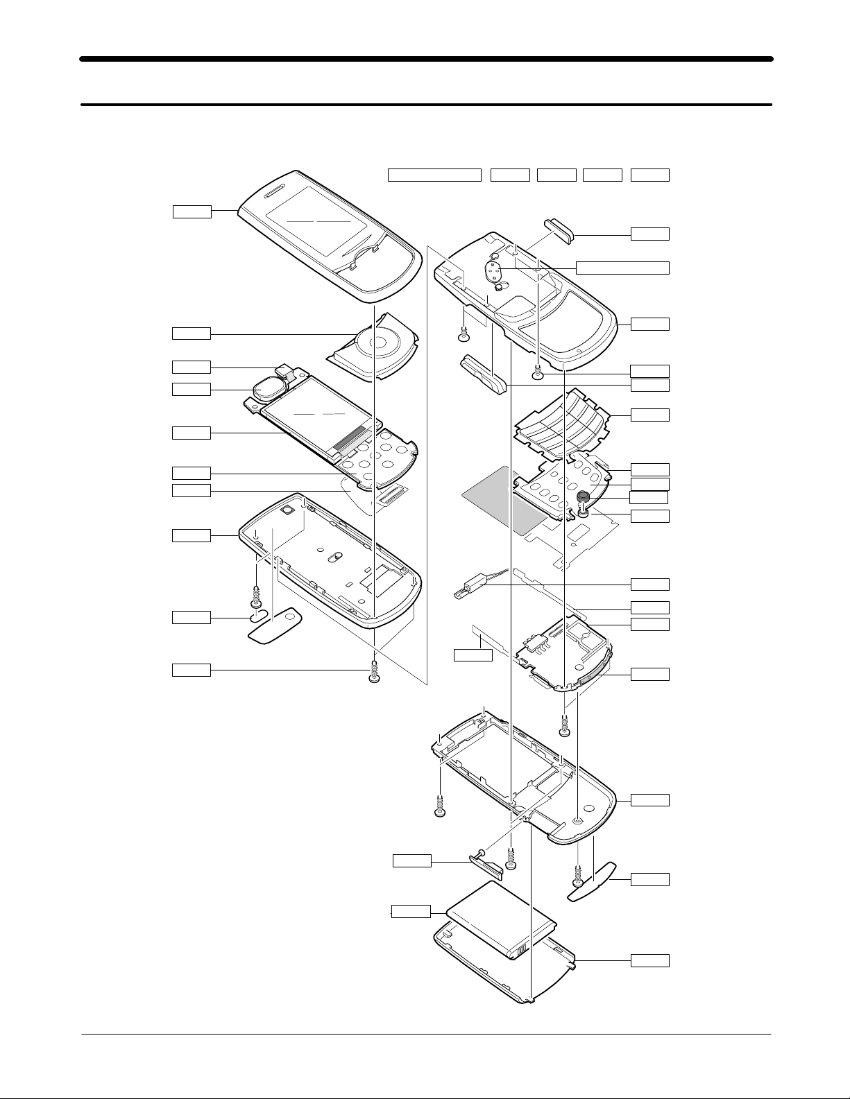
Exploded View and Parts List
2.
Cellular phone Exploded View
2-1.
QFU01
QKP02
QCA01
QSP01
QLC01
QME02
QPC01
QFL01
QHI01 : GH98-04515A
QCR57 QFL01 QFR01
=
++
QHI01
+
QCK01
QHI01 : GH98-05660A
QFR01
QCR57
QVO01
QKP01
QBR04
QME01
QMI01
QMI03
QSC01
QCR05
QMO01
QVK01
QMP01
QVK02
QAN02
QRE01
QIF01
QRF01
QBA01
QBA00
2-1
SAMSUNG Proprietary-Contents may change without notice
This Document can not be used without Samsung's authorization
Main Electrical Parts List
Cellular phone Parts list
2-2.
Design LOC
QAN02
QBA00
QBA01
QBR04
QCA01
QCK01
QCR05
QCR05
QCR05
QFU01
QKP01
QKP02
QLC01
QME02
QMO01
QMP01
QPC01
QRF01
QSC01
QSP01
QVK01
QVK02
QVO01
QME01
QRE01
QHI01
Discription SEC CODE
INNER BATTERY PACK-800MAH,BLK, GH43-02719A
ELA UNIT-SGH_M600 LCD MODULE
DOME SHEET-DOME SHEET9KEY GH59-04438A
KEY FPCB-SIDE POWER1KEY FPCB GH59-04440A
INTENNA-SGH_M600 GH42-01206A
PMO-BATT COVER GH72-39166A
ASSY KEYPAD-BRACKET GH98-04516A
UNIT-CAMERA GH59-04415A
PMO-POWER KEY GH72-39161A
SCREW-MACHINE
SCREW-MACHINE
SCREW-MACHINE
6001-001478
6001-001478
6001-001478
ASSY COVER-SLIDE UPPER GH98-04439A
ASSY KEYPAD-MAIN(SER/DSA) GH98-05516A
ASSY KEYPAD-SUB(XEF/DSA) GH98-04443A
(
GH96-02764A
MOTOR DC-SGH-M600 GH31-00340A
PBA MAIN-SGHM600 GH92-03632A
MEA-FPCB KIT GH97-07862A
ASSY COVER-RF GH98-05002A
PMO-SCREW CAP GH72-39157A
SPEAKER
3001-002165
KEY FPCB-SIDE VOLUME GH59-04439A
PMO-VOLUME KEY GH72-39162A
KEY FPCB-KEY PBA(34KEY) GH59-04437A
QMI01 AS-MIC GH81-06707A
QMI03 AS-MIC RUBBER GH81-06708A
ASSY COVER-REAR GH98-04442A
QIF01 PMO-IF COVER GH72-39164A
QCR57 SCREW-MACHINE
ASSY HINGE GH98-04515A
6001-002001
QFL01 ASSY COVER-SLIDE LOWER GH98-04440A
QFR01 ASSY COVER-FRONT GH98-04441A
QHI01 ASSY HINGE-SLIDE GH98-05660A
2-2
SAMSUNG Proprietary-Contents may change without notice
This Document can not be used without Samsung's authorization
Main Electrical Parts List
ADAPTOR-ATADS10EBE,BLK,EU GH44-01702A
MANUAL USERS-EU RUSSIAN GH68-15270A
MPR-REMOVE TAPE LCD GH74-13804A
Discription SEC CODE
BAG PE
6902-000297
EARPHONE-B-TYPE GH59-04557A
LABEL(P)-UNIT SEAL GH68-00518B
MANUAL-SFC GH68-04336A
LABEL(R)-WATER SOAK GH68-09361A
LABEL(R)-MAIN(SER) GH68-15468B
BOX(P)-UNIT MAIN(SER) GH69-05650C
MPR-TAPE LCD
A
GH74-24670A
MPR-INSU TAPE GH74-27151A
MPR-INSU TAPE GH74-28075A
MPR-INSU TAPE GH74-28241A
TAPE-FPCB BACK GH74-33643A
VINYL-BOHO MAIN GH74-33869A
2-3
SAMSUNG Proprietary-Contents may change without notice
This Document can not be used without Samsung's authorization

Main Electrical Parts List
2-4
SAMSUNG Proprietary-Contents may change without notice
This Document can not be used without Samsung's authorization
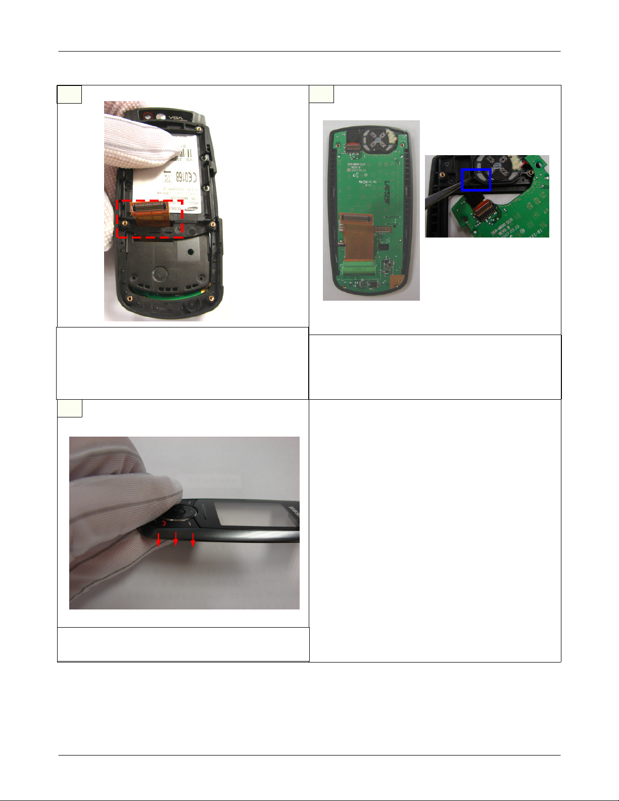
2-3.
Main Electrical Parts List
Assembly
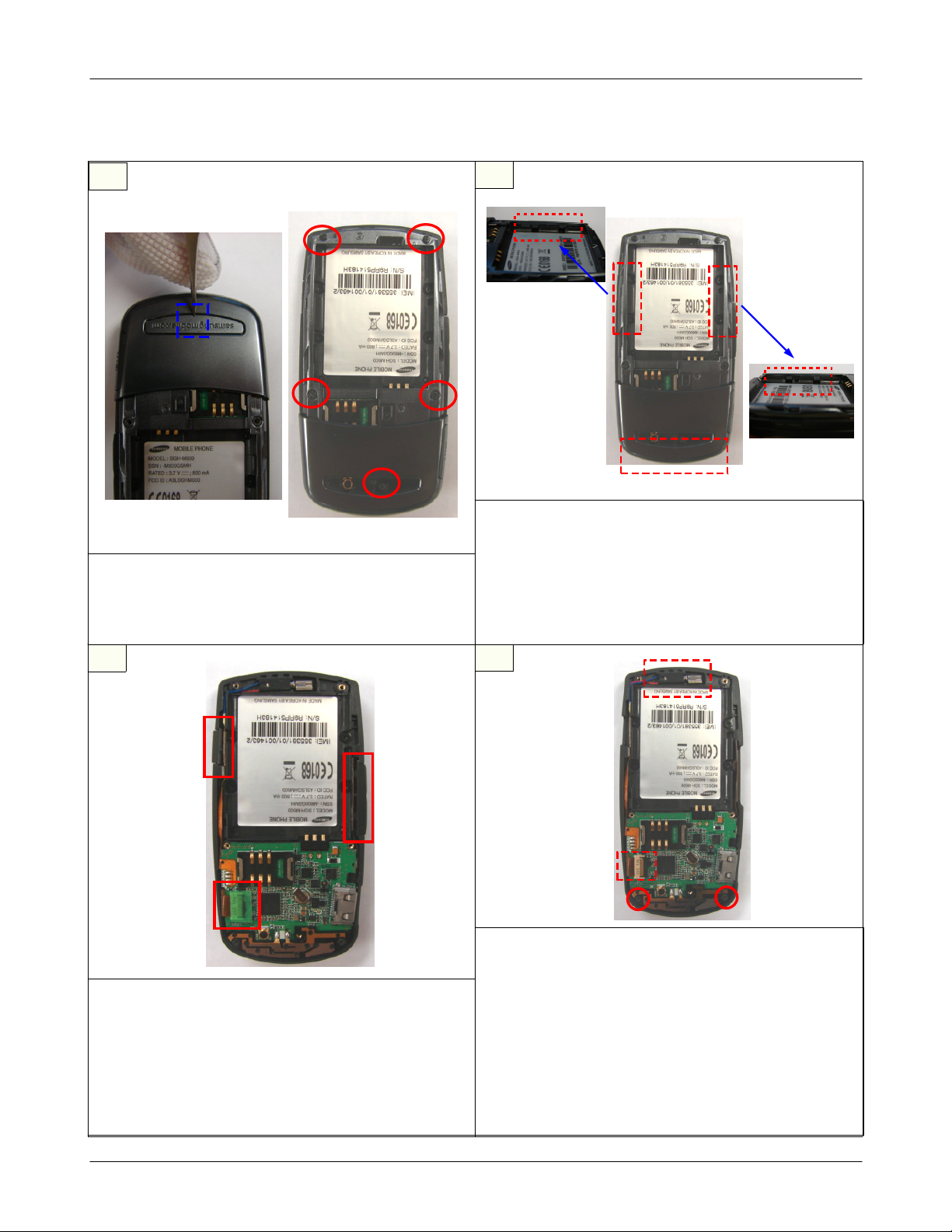
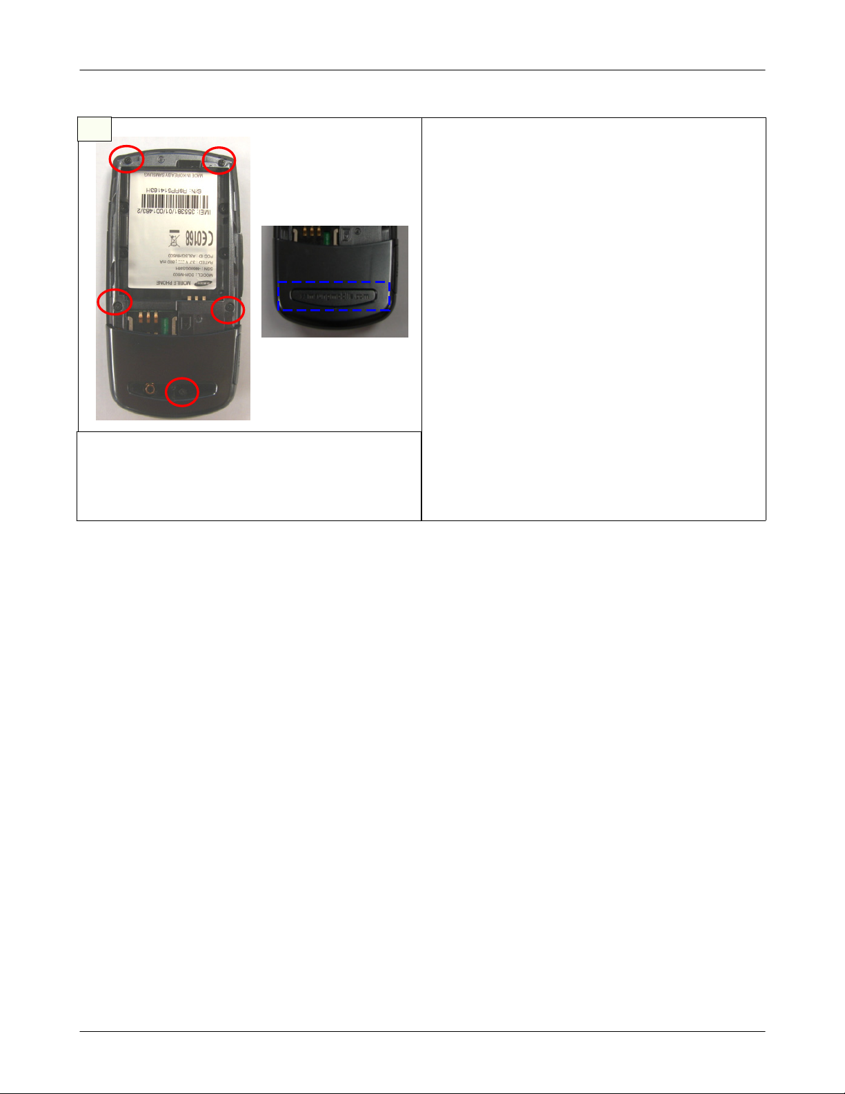
1
Remove RF cover using the pointed tool.
1)
Disjoint the REAR Screw of5Points.
2)
caution
※
Be careful for scratch
1)
2
pic
<
1>
Disjoint REAR's lockers just like pictures
1)
below.(pic1&pic
Disjoint other lockers too.
2)
caution
※
Be careful for scratch
1)
Be careful for demage of lockers.
2)
2)
pic2>
<
3
Disjoint volume-key&pwr-key.
1)
Remove the green tape on the connector
2)
of key-pad FPCB.
caution
※
Be careful for crumpling&crack of key-pad
1)
FPCB.
4
Disjoint the intenna screw of2points.
1)
Disjoint the key-pad FPCB from connector.
2)
Take off the motor from the FRONT plastic
3)
using tweezers and disjoint pwr-key FPCB
volume key FPCB from the FRONT plastic.
caution
※
Be careful for scratch.
1)
Be careful for the damage on the WIRE of
2)
Motor
2-5
&
SAMSUNG Proprietary-Contents may change without notice
This Document can not be used without Samsung's authorization
Main Electrical Parts List
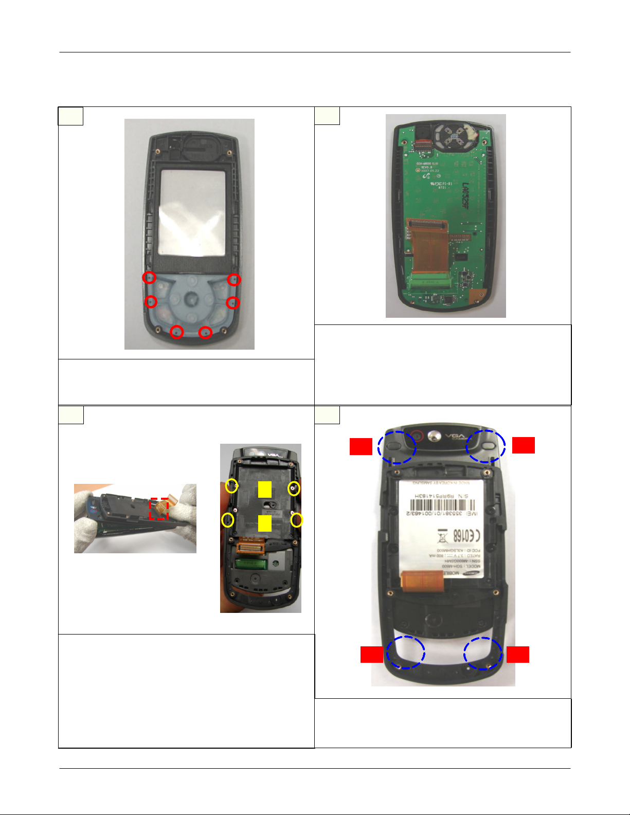
5
Disjoint the LCD FPCB&PBA like the
1)
pictrue below.
Disjiont the PBA from the FRONT plastic.
2)
caution
※
Be careful for the FPCB's crack
1)
6
Disjoint the key-pad bracket from the
1)
FRONT plastic.
Remove the Key-pad rubber.
2)
caution
※
Be careful for scratch
1)
7
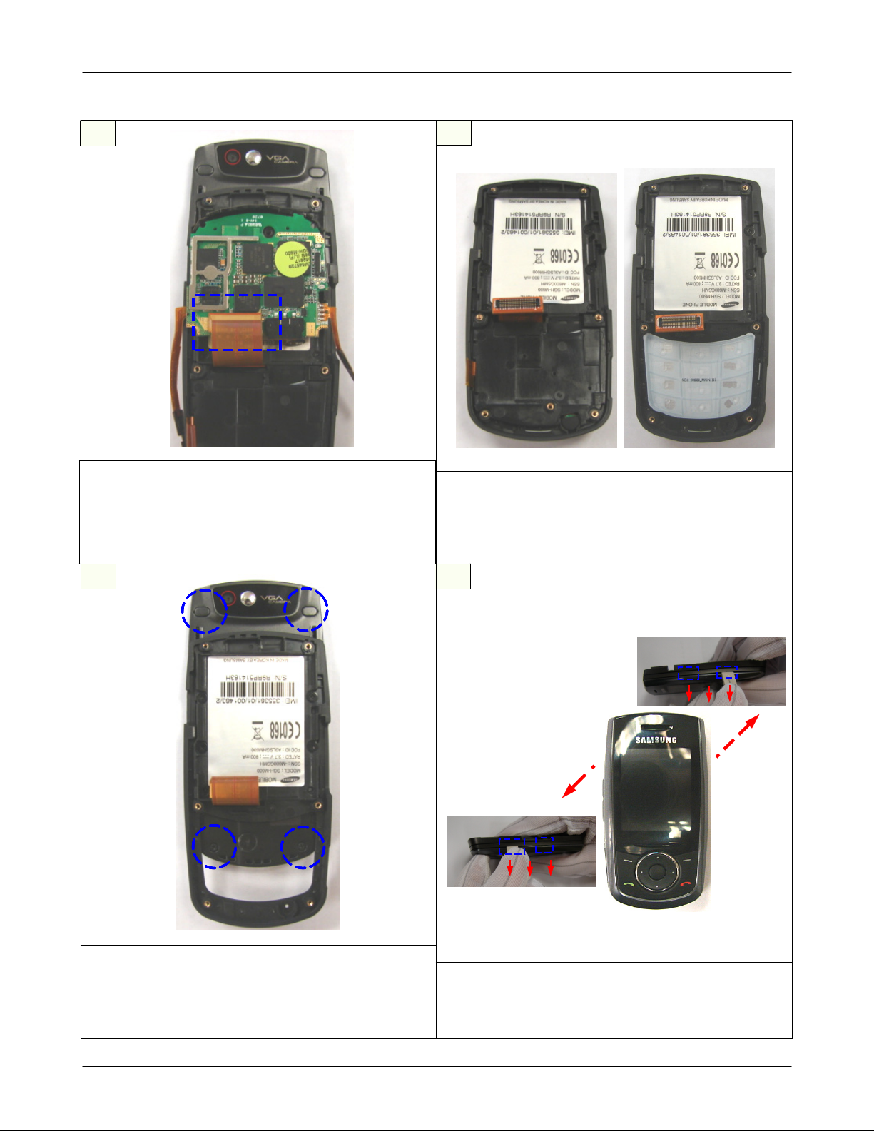
Slide up like the picture below.
1)
Disjoint screw caps using tweezers.
2)
Disjoint LOWER plastic Screw of4points.
3)
caution
※
Be careful for scratch.
1)
8
Using the Disassemble tool, Disjoint the UPPER
1)
plastic&LOWER plastic like the pictures below.
caution
※
Be careful for scratch.
1)
2-6
SAMSUNG Proprietary-Contents may change without notice
This Document can not be used without Samsung's authorization
Main Electrical Parts List
9
1) Slide up like the picture below.
2) Disjoint the Hinge ASSY from the UPPER
plastic.
caution
※
Be careful for the LCD FPCB's crack.
1)
10
<
1>
Pic
Lift up the LCD PBA slightly&Remove the
1)
camera module,
Disjoint the speaker.
2)
caution
※
Be careful for the demage of camera&speaker
1)
11
Disjoint the Navi-key from the UPPER
1)
plastic.
2-7
SAMSUNG Proprietary-Contents may change without notice
This Document can not be used without Samsung's authorization
Disassembly
2-4.
Main Electrical Parts List
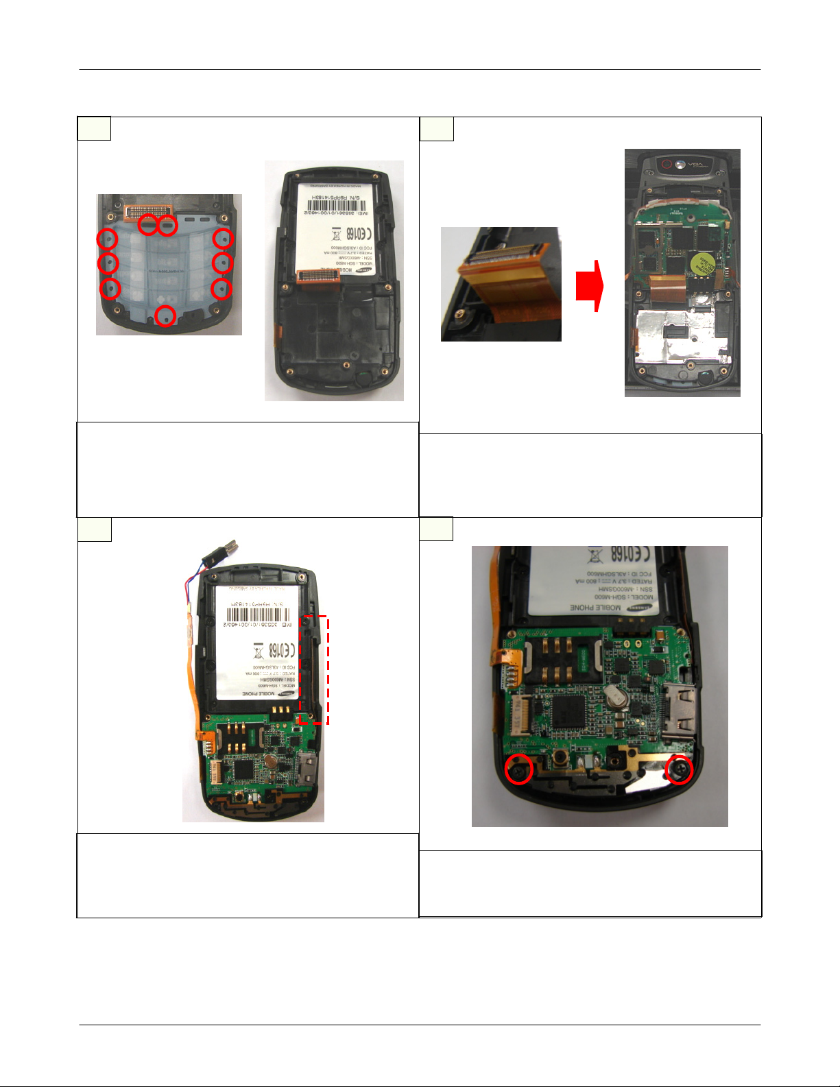
1
1) Put the NAVI key like the picture below.
caution
※
Put the hole of NAVY key to UPPER
1)
2
Put the speaker&camera.
1)
Put the LCD-PBA on the UPPER plastic.
2)
caution
※
Check the fabrication status of SPK&CAM
1)
Be careful for the CAM FPCB's crack.
2)
3
1) Slide up like the picture below.
2) Insert the FPCB through the hole at Hinge.
and Push up the LOWER plastic.
3) Push #1 & #2 in numerical order.
caution
※
Be careful for the scratch and crack of FPCB.
1)
2) Be careful for the demage of LCD.
4
1
2
1
3 4
Joint the4screws
1)
caution
※
Be careful for scratch.
1)
in numerical order.
2
2-8
SAMSUNG Proprietary-Contents may change without notice
This Document can not be used without Samsung's authorization
Main Electrical Parts List
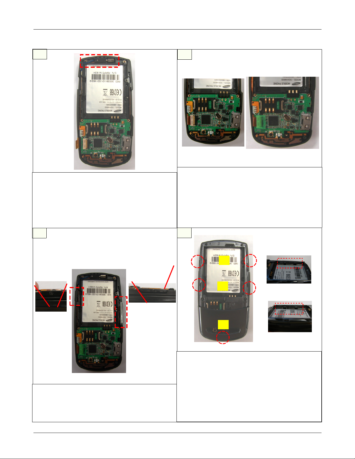
5
Put the key-pad on the FRONT.
1)
Put the MIC and bracket like the picture
2)
below..
caution
※
Check the flatness of MIC.
1)
6
pic
<
1>
Fold the FPCB like the picture below.
1)
Joint the FPCB&connector.
2)
caution
※
Check the connection of FPCB.
1)
<
pic
2>
7
FoldthevolumekeyFPCB&Insert the
1)
volume key into the slot.
caution
※
Volume key must be inserted fully.
1)
8
Joint the2intenna screws.
1)
caution
※
Be careful for the scratch.
1)
2-9
SAMSUNG Proprietary-Contents may change without notice
This Document can not be used without Samsung's authorization
Main Electrical Parts List
9
Put the pwr-key like the picture below.
1)
Put the motor like the picture below.
2)
Wires must be in order like the picture
below.(blue wire: top, red wire: bottom)
caution
※
Wires must be in order.
1)
10
Insert the
1)
along the SILK LINE.
Put the green TAPE on the connector.
2)
caution
※
Check the connection of FPCB.
1)
Be careful for the scratch and crack of FPCB.
2)
key FPCB to the CONNECTOR
3*4
11
Insert the pwr-key.
1)
Insert the volume-key.
2)
caution
※
Be careful for the direction of vol-key, pwr-key
1)
12
3
2
1
Insert the
1)
along the SILK LINE.
Put the green TAPE on the connector.
2)
caution
※
vol-key, pwr-key FPCB must be covered with
1)
REAR COVER plastic.
Be careful not to give demage to locker.
2)
key FPCB to the CONNECTOR
3*4
<
pic
<
pic
1>
2>
2-10
SAMSUNG Proprietary-Contents may change without notice
This Document can not be used without Samsung's authorization
13
Joint the5screws of REAR COVER plastic.
1)
Main Electrical Parts List
Joint the RF cover.
2)
caution
※
Be careful for the scratch.
1)
2-11
SAMSUNG Proprietary-Contents may change without notice
This Document can not be used without Samsung's authorization
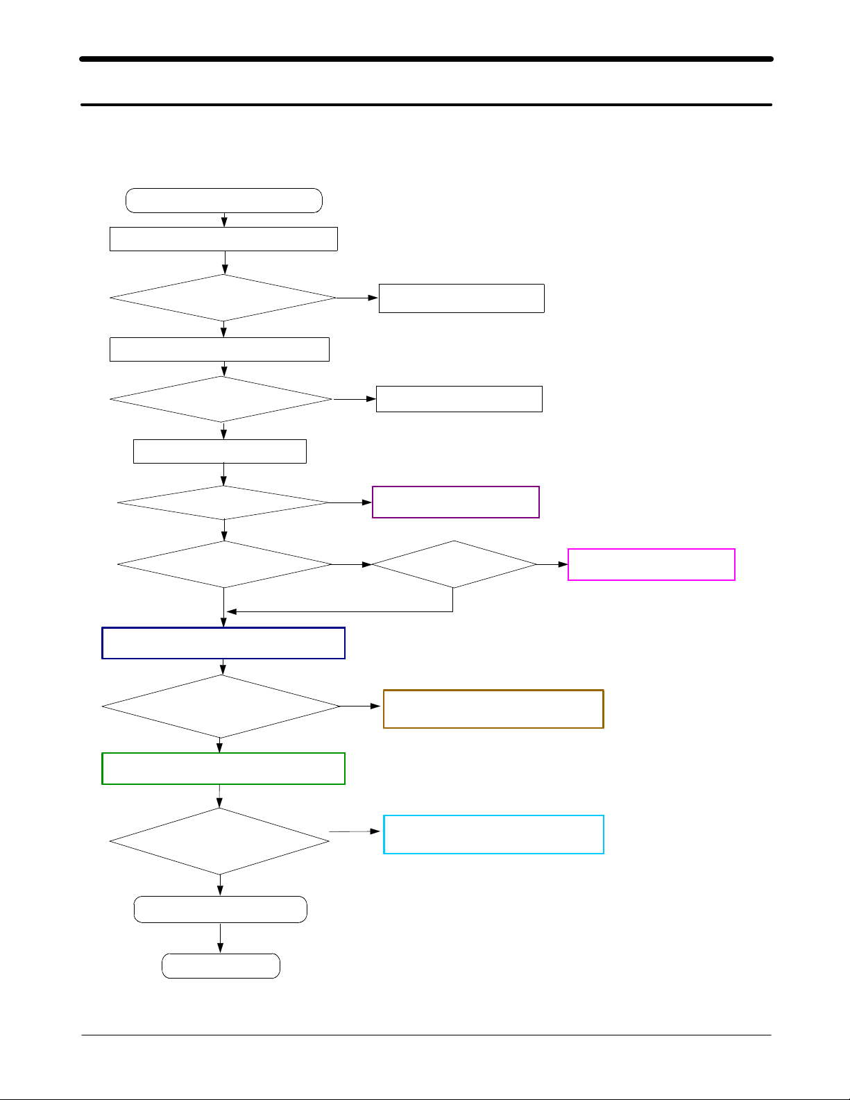
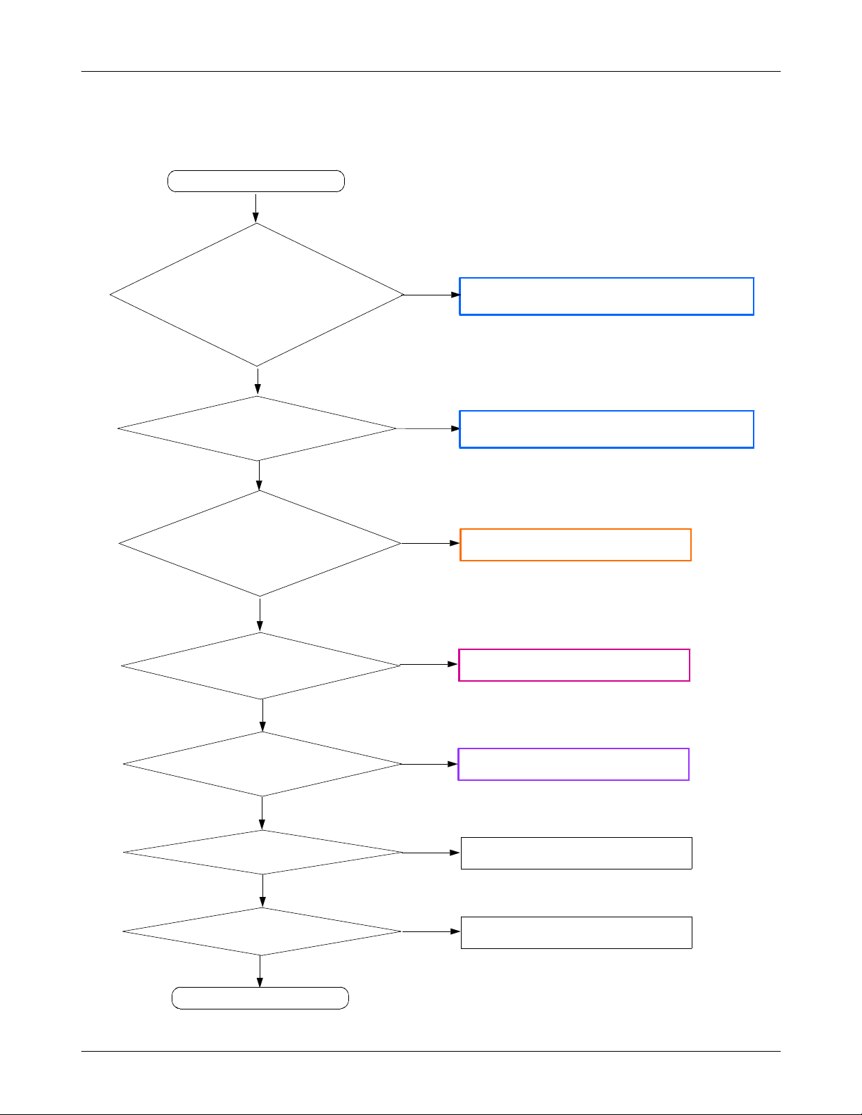
3. Flow Chart of Troubleshooting
Baseband
3-1.
3-1-1.
Power ON
Power On' does not work
'
Check the current consumption
Yes
Current consumption
Check the Vbat Voltage
Voltage
Check the pin of UCP
Pin#J12
Pin#A13 and pin#A14
>= 100
=2.8V
mA
Yes
>=3.3V
Yes
>= 2.8V
Yes
300
No
No
No
No
Download again
Charge the Battery
Check UCP
300
pin#G11
and
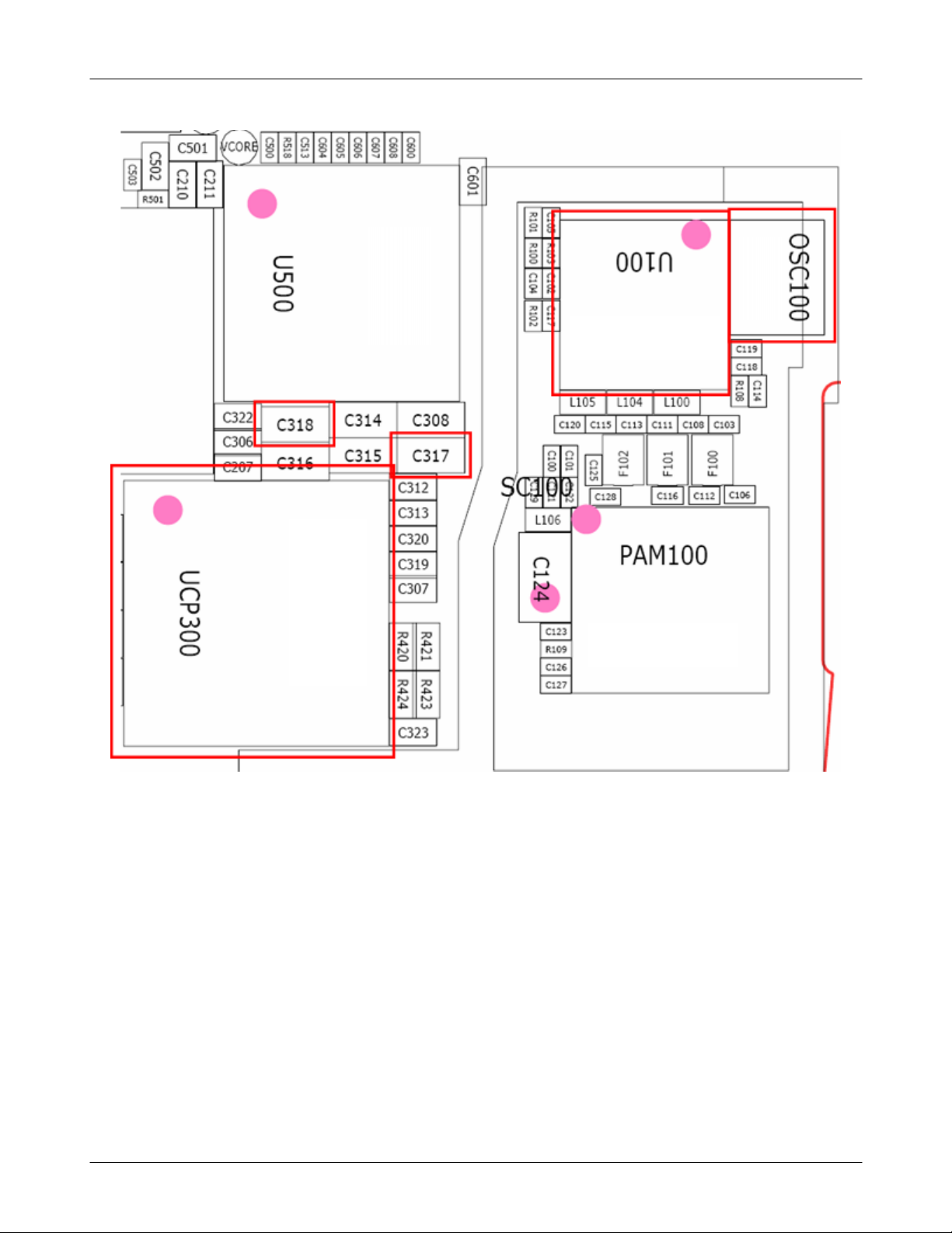
C317
=1.8V
No
Check UCP
300
and
C318
Yes
Check the clock signal at pin#
Freq
Vrms
Vpp
Check the clock signal at pin#8of
Freq
Check the initial operation
≒
END
=26
>=300
900
=13
MHz
mV
Yes
Mz
Yes
mV
30 #31ofU100
U100
No
No
Yes
Check the clock generation circuit
relatedtoOSC
(
Check
100)
U100
3-1
SAMSUNG Proprietary-Contents may change without notice
This Document can not be used without Samsung's authorization
Flow Chart of Troubleshooting
3-2
SAMSUNG Proprietary-Contents may change without notice
This Document can not be used without Samsung's authorization
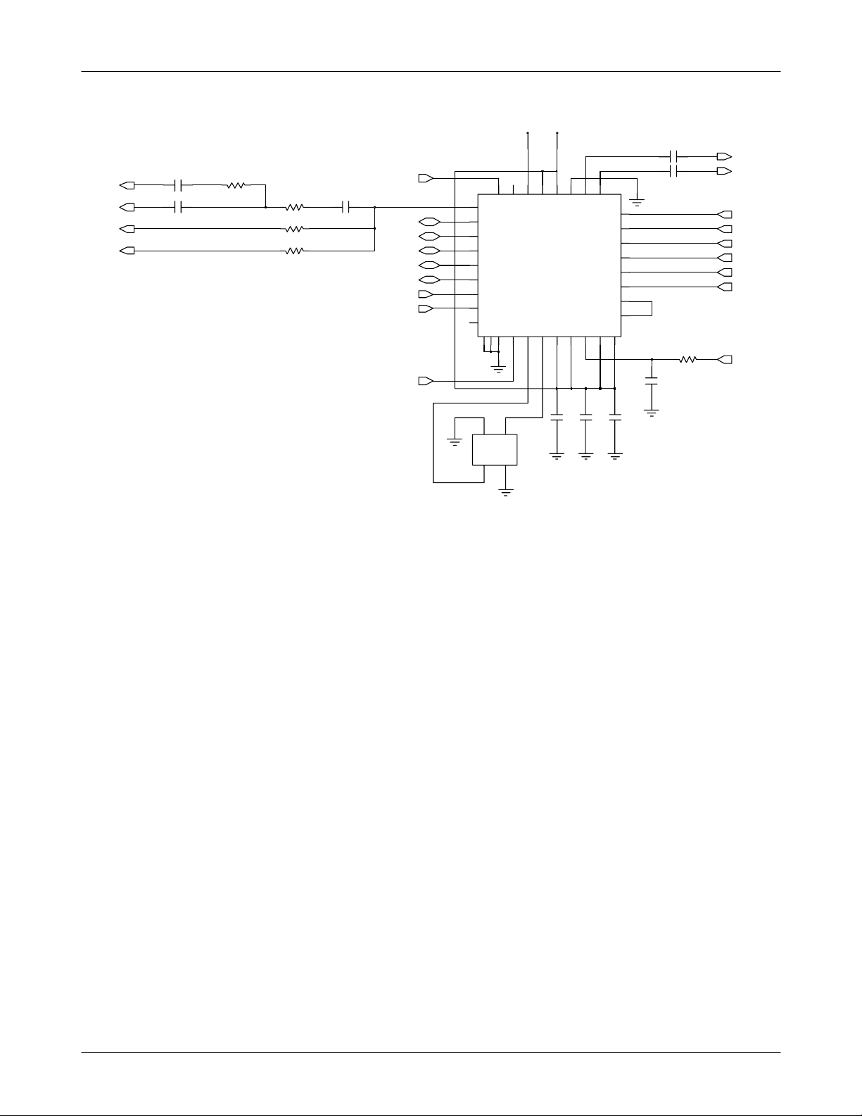
VCCD_2.9V
Flow Chart of Troubleshooting
VRF_2.9V
CLK13M_TR
CLK13M_MC
CLK13M_YMU
CLK13M_BK
C104
C100
R100C102
R101
R102
R103
C105
RF_EN
RTX_I_P
RTX_I_N
RTX_Q_P
RTX_Q_N
SBDT
SBCK
XOENA
910
XOUT
8
BIP
7
BIN
6
BQP
5
BQN
4
SDIO
SBI
3
_SEN
2
SCLK
1
NC
36
C
N
35
12
13
11
T
N
D
P
_
D
O
I
E
D
V
S
V
E
R
_
U100
2
1
L
L
N
A
A
D
C
N
N
G
3334
T
E
T
X
X
X
30
29
32
31
1615
14
L
D
D
V
D
D
V
H
D
O
N
O
F
F
G
R
R
RFIPP
RFIPN
RFIDP
RFIDN
RFIEP
RFIEN
RFIAP
RFIAN
V
I
D
C
D
D
F
X
V
A
27
28
26
25
C101
17
18
19
20
21
22
23
E
24
D
O
M
X
R108
C114
GSM_PAM_IN
DPCS_PAM_IN
PCS_LNA_IN_P
PCS_LNA_IN_N
DCS_LNA_IN_P
DCS_LNA_IN_N
GSM_LNA_IN_P
GSM_LNA_IN_N
AFC
OSC100
4
GND2
HOT
1
3
HOT
GND1
2
C117
C118
C119
3-3
SAMSUNG Proprietary-Contents may change without notice
This Document can not be used without Samsung's authorization
Flow Chart of Troubleshooting
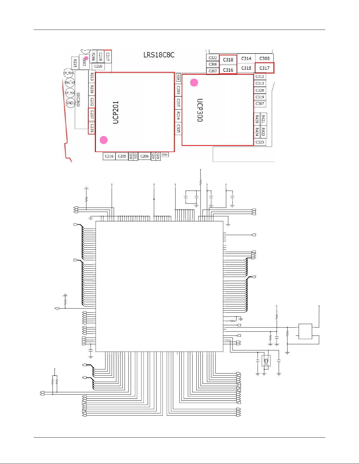
3-1-2.
Initial
Initial Failure
Yes
The pin#G11 of UCP
1.8V
the pin#J12 of UCP
2.8V ?
Is the pin#K9 of UCP
Low→High"
"
There is
32.768
forms at the C237and C2
300 =
and
300 =
Yes
?
Yes
kHz wave
300
No
if it has some problem, it is to be replaced.)
(
No
if it has some problem, it is to be replaced.)
(
No
38
Check the UCP
Check the UCP
Check the UCP20
300
300
1
Yes
Is the pin
The voltage is"High" at the
C316,C317,C318
LCD display is O.K
of UCP
#G4
is"High"
Yes
Yes
Yes
Sound is O.K
Yes
END
201
No
No
No
No
Check the UCP20
Check the UCP
Check the LCD part
Check the Audio part
1
300
3-4
SAMSUNG Proprietary-Contents may change without notice
This Document can not be used without Samsung's authorization
Flow Chart of Troubleshooting
VCCD_1.8V
D_SCL
D_SDA
R218
A1(21)
VCCD_2.9V
1
2
7
8
1
1
1
C
D
F
C
I
A
A
B
C
K
T
T
S
D
C
S
S
R
D
V
R
V
V
CKO/IACK/ERAMHI
XTIC_MODE
XCPTSTSTOP_CKO
XRTCALARM_N
N
T
S
S
K
I
XOSC32OUT
M
R
C
D
T
T
T
T
_
_
_
_
P
P
P
P
C
C
C
C
X
X
X
X
9
8
7
7
F
D
C
G
VRTC_3VVCCD_2.9V
C215
DB#15
DB#14
DB#13
DB#12
DB#11
DB#10
XBSWN
X1RTC
X2RTC
O
D
T
_
P
C
X
3
1
D
C216
VREF
CLK13M_TR
TR_RST
F12
TDO
F15
TRST
H12
TDI
G12
TMS
H13
TCK
G15
L12
K11
N4
INT#0
R12
IO7
U5
RWN
T17
AB#8
T14
AB#7
R14
AB#6
P12
AB#5
P11
AB#4
N11
AB#3
R13
AB#2
M10
AB#1
U13
AB#0
P10
R11
T11
U11
M8
N8
N7
DB#9
P7
DB#8
M6
DB#7
R7
DB#6
T7
DB#5
U7
DB#4
P6
DB#3
R6
DB#2
U6
DB#1
P5
DB#0
D12
R214
M12
D11
XAG3
E11
XAG2
A11
XAG1
B11
XAG0
B7
A7
D10
E8
C6
OSC200
A(8)
A(7)
A(6)
A(5)
A(4)
A(3)
A(2)
A(1)
A(0)
D(15)
D(14)
D(13)
D(12)
D(11)
D(10)
D(9)
D(8)
D(7)
D(6)
D(5)
D(4)
D(3)
D(2)
D(1)
D(0)
ICHRG
TR_RST
RTC_ALARM
CLK32K
CP_TDO
TR_RST
CP_TDI
CP_TMS
CP_TCK
DEBUG_DSR
EAR_SWITCH
AS1
JACK_IN
PWR_KEEP
SIM1_RST
CHG_OFF
FLASH_RST
BL_EN
BP_VF
UP_CS
UP_SCLK
UP_SDO
UP_SDI
TR_RST
DSP_INT
DSP_IO
DSP_RWN
A(8:0)
D(15:0)
VBAT
R213
R215
1M
C232
R216
4
1
C237
12PF
C238
3
2
VCCB_2.9V
1
4
VOUT
VCC
U602
3
2
GND
NC
VCCD_1.8V
R205
BK_RST
A1(22)
A1(23)
5
4
3
7
0
1
7
1
1
7
1
N
L
1
2
2
N
C
C
2
5
N
N
A
D1(0:15)
A1(0:20)
R219
R212
CP_CSROMEN
CP_CSRAMEN
DLC_DETECT
UPPER_BYTE
KEY_COL(0:4)
KEY_ROW(0:4)
DEBUG_DTR
DEBUG_RTS
DEBUG_TXD
DEBUG_RXD
DEBUG_CTS
BK_CS
YMU_EN
CP_WEN
CP_OEN
BK_LCD_BY
INTRQ
RADIO_INT
FLIP_SNS
YMU_IRQ
CHG_DET
SDS_TXD
SDS_RXD
SIM_DATA
SIM1_CLK
D1(0)
D1(1)
D1(2)
D1(3)
D1(4)
D1(5)
D1(6)
D1(7)
D1(8)
D1(9)
D1(10)
D1(11)
D1(12)
D1(13)
D1(14)
D1(15)
A1(0)
A1(1)
A1(2)
A1(3)
A1(4)
A1(5)
A1(6)
A1(7)
A1(8)
A1(9)
A1(10)
A1(11)
A1(12)
A1(13)
A1(14)
A1(15)
A1(16)
A1(17)
A1(18)
A1(19)
A1(20)
AS2
C234
A6
B5
F8
F7
C5
D6
E7
D5
C4
B4
B3
C1
C2
D2
D3
E3
B13
F11
E14
D15
B15
C14
A16
A15
B17
C17
D16
F14
G14
G13
G17
J12
K12
K13
K14
L14
L15
L16
A12
A13
M15
M14
M11
N14
C13
P16
P15
T15
M9
T5
P2
N2
KEY_COL(0)
KEY_COL(1)
KEY_COL(2)
KEY_COL(3)
KEY_COL(4)
KEY_ROW(0)
KEY_ROW(1)
KEY_ROW(2)
KEY_ROW(3)
KEY_ROW(4)
XCP_D0
XCP_D1
XCP_D2
XCP_D3
XCP_D4
XCP_D5
XCP_D6
XCP_D7
XCP_D8
XCP_D9
XCP_D10
XCP_D11
XCP_D12
XCP_D13
XCP_D14
XCP_D15
XCP_A0_BEON
XCP_A1
XCP_A2
XCP_A3
XCP_A4
XCP_A5
XCP_A6
XCP_A7
XCP_A8
XCP_A9
XCP_A10
XCP_A11
XCP_A12
XCP_A13
XCP_A14
XCP_A15
XCP_A16
XCP_A17
XCP_A18
XCP_A19
XCP_A20
XCP_A21
XCP_CSROMEN
XCP_CSRAMEN
XPA0/CS1N
XPA1/CS2N
XPA2/CS3N
XPA3/CS4N
XCP_WEN
XPA4/OEN
XPA5/WAITN
XPA6/BE1N
XPA7/IRQ1
XPA8/IRQ2
XPA9/IRQ3
XPA10/IRQ4
S
_
C
5
_
3
3
A
2
P
A
X
_
6
3
A
P
X
F
M
M
R
A
O
E
R
R
I
I
P
_
_
_
S
S
S
C
C
C
_
_
_
R
R
R
T
T
T
/
/
/
]
]
]
0
1
2
[
[
[
B
B
B
K
K
K
_
_
_
P
P
P
C
C
C
4
5
4
L
L
M
6
1
9
8
1
1
L
K
H
J
L
L
M
L
L
S
S
S
S
S
S
S
N
D
0
S
S
S
S
S
S
S
D
S
V
V
V
V
V
V
V
V
C
_
2
3
A
P
X
A
P
M
C
0
C
D
0
P
1
T
_
E
I
E
E
T
_
X
O
K
Z
ZI
N
S
E
L
I
R
S
C
N
G
S
C
P
X
X
_
_
_
_
_
_
_
T
R
R
R
R
R
R
R
R
A
A
T
T
T/]
T/]
T/]
T
T
/
/
]
3
[
B
K
_
P
C
1
T
D
D
/
/
]
]
]
RI/
R
4
8[
9[
7[
5[
6
I
[
[
/
B
B
B
B
B
B
2
1
1
1
K
K
K
K
K
K
_
_
_
_
_
_
A
A
P
P
P
P
P
P
P
P
C
C
C
C
C
X
C
X
3
4
1
5
3
2
3
3
T
T
K
P
N
N
R
U
VCCD_1.8V
VCORE
0
1
1
7
1
6
7
K
J
H
H
G
S
S
S
S
S
S
S
S
S
S
V
V
V
V
V
6
7
6
9
1
1
1
3
2
5
6
A
G
A
F
R
R
A
C
S
S
S
S
D
D
D
D
S
S
S
S
D
D
D
D
V
V
V
V
V
V
V
V
C217
6
5
6
7
6
4
3
1
1
1
4
1
R
R
T
D
D
D
D
D
D
V
V
V
1
1
1
1
2
1
E
E
N
E
B
G
U
U
E
E
E
E
E
D
D
D
D
D
D
D
D
D
D
D
V
V
D
D
D
V
V
V
V
V
UCP201
A
T
A
K
L
D
A
_
C
0
_
0
M
S/
M
1
0
0
0
1
0
X
X
T
R/
M
M
/
I
I
/
/
5
6
1
0
1
1
3
3
A
A
A
A
P
P
P
P
X
X
4
3
3
1
L
F
E
H
S
A
/
1
1
M
M
T
K
X
X
L
A
OI/
OI/
T
R
/
/
C
D
3
9
8
4
_
_
1
2
2
1
M
MI
I
A
A
A
A
S
P
P
P
S
P
1
5
3
6
0
2
1
1
F
G
G
G
N
U
T
T
K
E
A
C
S
3
2
O
I
D
S
E
_
M
M
M
M
_
1
R
_
_
P
W
W
_
P
P
M
C
P
P/
H
/
/
1
C
S
C/
/
/
1
4
3
S
M
2
0
9
2
2
2
A
2
2
1
A
A
A
W
L
A
A
A
P
P
P
F
P
P
P
P
X
X
X
X
6
5
4
2
5
6
1
4
J
L
L
F
K
H
R
H
VCCD_2.9V
R204
4.7
C218
6
5
0
0
1
1
2
1
8
1
1
1
G
E
E
B
F
M
U
P
L
L
F
E
E
E
E
E
L
L
E
D
D
D
D
D
P
P
R
D
D
D
D
D
D
D
V
V
V
V
V
V
_
_
X
S
D
S
D
V
V
IOBIT[2]/VEC[3]/EROMHI
IOBIT[1]/VEC[4]/PLLTOA
K
A
L
B
C
Q
K
Q
_
E
E
C
0
1
1
Q
R
R
A
M
M
R
M
_
_
_
D
O/
T/
S
T/
T
O
/
/
/
/
7
5
3
7
8
4
6
1
2
3
2
1
3
2
A
A
A
A
A
A
N
P
P
P
P
P
P
P
7
7
3
4
2
3
4
1
1
1
E
G
G
M
P
N
M
3-5
SAMSUNG Proprietary-Contents may change without notice
This Document can not be used without Samsung's authorization
 Loading...