

Samsung KS88P4632, KS88C4632, KS88C4616 Datasheet

KS88C4616/C4632/P4632 PRODUCT OVERVIEW
1 PRODUCT OVERVIEW
SAM8 PRODUCT FAMILY
Samsung's new SAM8 family of 8-bit single-chip CMOS microcontrollers offers a fast and efficient CPU, a wide
range of integrated peripherals, and various mask-programmable ROM sizes.
A dual address/data bus architecture and a large number of bit- or nibble-configurable I/O ports provide a flexible
programming environment for applications with varied memory and I/O requirements. Timer/counters with
selectable operating modes are included to support real-time operations. Many SAM8 microcontrollers have an
external interface that provides access to external memory and other peripheral devices.
A sophisticated interrupt structure recognizes up to eight interrupt levels. Each level can have one or more
interrupt sources and vectors. Fast interrupt processing (within a minimum six CPU clocks) can be assigned to
one interrupt level at a time.
KS88C4616/C4632 MICROCONTROLLER
The KS88C4616/C4632 single-chip 8-bit microcontroller is designed for useful 10-bit resolution A/D converter,
UART, SIO, ZCD extended PWM application field. Its powerful SAM87 CPU architecture includes. The internal
register file is logically expanded to increase the on-chip register space.
The KS88C4616/C4632 has 16/32 K bytes of on-chip program ROM. A sophisticated bus interface enables
access to external memory and other peripherals when you use the chip in ROM-less mode. Following
Samsung's modular design approach, the following peripherals are integrated with the SAM87 core:
— Large number of programmable I/O ports (total 56 pins)
— One asynchronous UART module
— One synchronous SIO module
— Analog-to-digital converter with eight input channels and 10-bit resolution
— One 8-bit basic timer for watchdog function
— One 8-bit timer/counter with three operating modes (timer 0)
— One 8-bit timer for zero-cross detection circuit (timer 2)
— Two general-purpose 16-bit timer/counters with four operating modes (timer module 1)
— PWM block with one capture module, 16-bit timer/counter, PWM extension mode, and two PWM outputs
— One zero cross detection module
The KS88C4616/C4632 is a versatile general-purpose microcontroller that is ideal for use in a wide range of
electronics applications requiring complex timer/counter, PWM, capture, SIO, UART and ZCD functions.
It is available in a 64-pin SDIP or 64-pin QFP package.
OTP
The KS88P4632 is an OTP (One Time Programmable) version of the KS88C4616/C4632 microcontroller. The
KS88P4632 microcontroller has an on-chip 32-Kbyte one-time-programmable EPROM instead of a masked
ROM. The KS88P4632 is comparable to the KS88C4616/C4632, both in function and in pin configuration.
1-1

PRODUCT OVERVIEW KS88C4616/C4632/P4632
FEATURES
CPU
• SAM87 CPU core
Memory
• 528-byte general purpose register area
• 16/32-Kbyte internal program memory
• ROM-less operating mode
External Interface
• 64-Kbyte external data memory area
• 64-Kbyte external program memory area
(ROM-less mode)
Instruction Set
• 79 instructions
• IDLE and STOP instructions added for
power-down modes
Instruction Execution Time
• 500 ns at 12 MHz f
(minimum)
OSC
Interrupts
• 21 interrupt sources and 21 vectors
• Eight interrupt levels
• Fast interrupt processing
Timer/Counters
• One 8-bit basic timer for watchdog function
• One 8-bit timer/counter with three operating
modes (timer 0)
• One 8-bit timer for the zero-cross detection
circuit
• Two 16-bit general-purpose timer/counters with
four operating modes (timer C and D)
UART
• One UART module
• Full duplex serial I/O interface with three UART
modes
A/D Converter
• Eight analog input pins
• 10-bit conversion resolution
• 20 µs conversion time (10 MHz CPU clock)
Zero Cross Detection Circuit
• Zero cross detection circuit that generates a
digital signal in synchronization with an AC
signal input
Buzzer Frequency Output
• 200 Hz to 20 kHz signal can be generated
General I/O
• Seven I/O ports (total 56 pins)
• Seven bit-programmable ports
PWM and Capture
• Two 14-bit PWM output
• One capture
Serial I/O
• One synchronous serial I/O module
• Selectable transmit and receive rates
• Selectable baud rate for Rx and Tx respectively
1-2
Oscillator Frequency
• 1 MHz to 12 MHz external crystal oscillator
• Maximum 12 MHz CPU clock
Operating Temperature Range
• – 40°C to + 85°C
Operating Voltage Range
• 2.7 V to 5.5 V
Package Types
• 64-pin SDIP, 64-pin QFP
KS88C4616/C4632/P4632 PRODUCT OVERVIEW
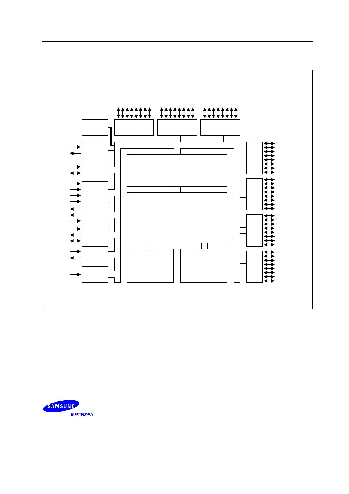
BLOCK DIAGRAM
X
X
OUT
T0CK
T0
TCG
TDG
TCCK
TDCK
PWM0
PWM1
CAPA
SI
SO
SCK
RxD
TxD
ADC0
-ADC7
P0.0-P0.7
(A8-A15)
Basic
Timer
IN
OSC
Timer
Timers
C and D
PWM/
CAP
SIO
UART
16/32-Kbyte
ROM
ADC
P1.0-P1.7
(AD0-AD7)
Port 1 Port 0Port 0
SAM8 BUS
P2.4/ZCD-P2.7/INT3
Port I/O and Interrupt
Control
SAM8 CPU
528-byte
Register File
P2.0-P2.3
Port 3
Port 4
Port 5
Port 6
P3.0-P3.7
P4.0/INT4P4.7/INT11
P5.0-P5.7
P6.0-P6.7
Figure 1-1. Block Diagram
1-3

PRODUCT OVERVIEW KS88C4616/C4632/P4632
PIN ASSIGNMENTS
P1.0/AD0
P0.7/A15
P0.6/A14
P0.5/A13
P0.4/A12
P0.3/A11
P0.2/A10
P0.1/A9
P0.0/A8
P4.7/INT11/TDG
P4.6/INT10/TCG
P4.5/INT9/TDCK
P4.4/INT8/TCCK
P4.3/INT7/CAPA
P4.2/INT6
P4.1/INT5/RxD
V
DD
V
SS
X
OUT
X
EA
P4.0/INT4
P3.7/TxD
RESET
P3.6/SO
P3.5/SI
P3.4/
SCK
P3.3/T0CK
P3.2/T0
P3.1/PWM1
P3.0/PWM0
P2.7/INT3
P2.6/INT2
1
2
3
4
5
6
7
8
9
10
11
12
13
14
15
16
17
18
IN
19
KS88C4616
KS88C4632
(64-SDIP-750)
20
21
22
23
24
25
26
27
28
29
30
31
32
64
63
62
61
60
59
58
57
56
55
54
53
52
51
50
49
48
47
46
45
44
43
42
41
40
39
38
37
36
35
34
33
P1.1/AD1
P1.2/AD2
P1.3/AD3
P1.4/AD4
P1.5/AD5
P1.6/AD6
P1.7/AD7
P5.7/ADC7
P5.6/ADC6
P5.5/ADC5
P5.4/ADC4
P5.3/ADC3
P5.2/ADC2
P5.1/ADC1
P5.0/ADC0
AV
SS
AV
REF
P6.7
P6.6
P6.5
P6.4
P6.3
P6.2
P6.1
P6.0
P2.0/
AS
P2.1/
DS
P2.2/R/
W
P2.3/
DM
P2.4/ZCD
P2.5/BUZ
1-4
Figure 1-2. Pin Assignment Diagram (64-Pin SDIP Package)

KS88C4616/C4632/P4632 PRODUCT OVERVIEW
P3.1/PWM1
P3.0/PWM0
P0.1/A9
P0.2/A10
P0.3/A11
P0.4/A12
P0.5/A13
P0.6/A14
P0.7/A15
P1.0/AD0
P1.1/AD1
P1.2/AD2
P1.3/AD3
P1.4/AD4
P1.5/AD5
64636261605958575655545352
P1.6/AD6
P4.7/INT11/TDG
P0.0/A8
P4.6/INT10/TCG
P4.5/INT9/TDCK
P4.4/INT8/TCCK
P4.3/INT7CAPA
P4.2/INT6
P4.1/INT5/RxD
V
DD
V
SS
X
OUT
X
EA
P4.0/INT4
P3.7/TxD
RESET
P3.6/SO
P3.5/SI
P3.4/
SCK
1
2
3
4
5
6
7
8
9
10
11
IN
12
KS88C4616
KS88C4632
(64-QFP-1420F)
13
14
15
16
17
18
19
51
50
49
48
47
46
45
44
43
42
41
40
39
38
37
36
35
34
33
P1.7/AD7
P5.7/ADC7
P5.6/ADC6
P5.5/ADC5
P5.4/ADC4
P5.3/ADC3
P5.2/ADC2
P5.1/ADC1
P5.0/ADC0
AV
SS
AV
REF
P6.7
P6.6
P6.5
P6.4
P6.3
P6.2
P6.1
20212223242526272829303132
W
P6.0
P3.2/T0
P3.3/T0CK
P2.5/BUZ
P2.4/ZCD
P2.7/INT3
P2.6/INT2
P2.1/DS
P2.3/DM
P2.2/R/
P2.0/AS
Figure 1-3. Pin Assignment Diagram (64-Pin QFP Package)
1-5
PRODUCT OVERVIEW KS88C4616/C4632/P4632
Table 1-1. KS88C4616/C4632 Pin Descriptions
Pin
Name
Pin
Type
Pin Description Circuit
P0.0–P0.7 I/O Bit-programmable I/O port for Schmitt trigger
input or push-pull, open-drain, output. Pull-up
resistors are assignable by software.
Port 0 can also be configured as external
interface address line A8–A15
P1.0–P1.7 I/O Same general characteristics as port 0.
Port 1 can also be configured as external
interface address/data lines AD0–AD7
P2.0–P2.3
I/O Bit-programmable I/O port for Schmitt trigger
input or push-pull output. P2.0–P2.3 can be
configured for external bus control signals.
P2.4–P2.7
P2.4–P2.7 are used for general I/O or for the
ZCD, BUZ, INT2 and INT3
P3.0–P3.7 I/O Bit-programmable I/O port for Schmitt trigger
input or push-pull output. Each port 3 pin has
an alternative function:
P3.0: PWM0 (PWM0 module output)
P3.1: PWM1 (PWM1 module ouptut)
P3.2: T0 (T0 capture input or PWM output)
P3.3: T0CK (timer 0 external clock input)
P3.4: SCK (SIO module input)
P3.5: SI (SIO module clock I/O)
P3.6: SO (SIO module output)
P3.7: TxD: SO1
(The T0 function for P3.2 is selected using the
T0CON register.)
P4.0–P4.7 I/O Bit-programmable I/O port for Schmitt trigger
input or push-pull output. Port 4 pins are used
external interrupts INT4–INT11 or for the
following share functions:
P4.1: RxD (UART module input)
P4.3: CAPA (capture input)
P4.4: TCCK (timer/counter C clock input)
P4.5: TDCK (timer/counter D clock input)
P4.6: TCG (timer C gate input)
P4.7: TDG (timer D gate input)
Number
1 8–1
(1, 64–58)–A8–A15
1 64–57
2
3
4 30–22
5 21, 15–9
Pin
Number
Share
Pins
(57–50)–AD0–AD7
38–35
(31–28)
–
AS, DS
DM, R/W
34–31
(27–24)
ZCD, BUZ
INT2, INT3
(See pin
(23–15)
description)
(See pin
(14–2)
description)
1-6

KS88C4616/C4632/P4632 PRODUCT OVERVIEW
Table 1-1. KS88C4616/C4632 Pin Descriptions (Continued)
Pin
Name
P5.0–P5.7 I/O Bit-programmable I/O port for Schmitt trigger
Pin
Type
Pin Description Circuit
input or push-pull, output. Pull-up resistors are
Number
6 49–56
Pin
Number
(42–49)
Share
Pins
ADC0–
ADC7
assignable by software. Port 5 pins can also be
used as A/D converter inputs.
P6.0–P6.7 I/O Individual pins are software configurable as
input or push-pull, open-drain, output. Pull-up
1 39–46
(32–39)
–
resistors are assignable by software.
AD0–AD7 I/O External interface address/data line 6 64–57
P1.0–P1.7
(57–50)
AS
DS
I/O External bus control signals 2 38–35
(31–28)
P2.0–P2.3
R/W
DM
ZCD I/O Zero cross detector input 2 34 (27) P2.4
BUZ I/O 200 Hz–20 kHz frequency output for buzzer
2 33 (26) P2.5
sound
PWM0
PWM1
I/O PWM output 3 30, 29
(23, 22)
P3.0–P3.1
T0 (CAP) I/O T0 capture input or PWM output 3 28 (21) P3.2
T0CK I/O External clock input for Timer 0 3 27 (20) P3.3
SCK I/O SIO clock signal 3 26 (19) P3.4
SI, SO I/O SIO data input/output 3 25, 24
P3.5–P3.6
(18, 17)
TxD I/O UART data output 3 22 (15) P3.7
INT2–INT3 I/O External interrupts: the triggering edge is
selectable.
INT4 I/O External interrupts: the triggering edge is
2 32, 31
P2.6–P2.7
(25, 24)
4 21 (14) P4.0
selectable.
RxD/INT5 I/O UART data input or external interrupt: the
4 15 (8) P4.1
triggering edge is selectable.
INT6
CAPA/INT7
I/O Capture module input or external interrupt: the
triggering edge is selectable.
4 14,13
(7, 6)
P4.2–P4.3
1-7

PRODUCT OVERVIEW KS88C4616/C4632/P4632
Table 1-1. KS88C4616/C4632 Pin Descriptions (Concluded)
Pin
Name
TCCK/INT8
TCDK/INT9
TCG/INT10
TDG/INT11
ADC0–
Pin
Pin Description Circuit
Type
I/O Timer/counter C and D clock input or external
interrupts: the triggering edge is selectable.
I/O Timer/counter C and D clock input or external
interrupts: the triggering edge is selectable.
I/O A/D converter inputs 5 49–56
ADC7
XIN, X
OUT
– System clock input and output pins – 19, 18
I System reset pin 7 23 (16) –
EA I External access (EA) pin with three modes:
0 V: Normal operation (internal ROM)
5 V: ROM-less operation (external interface)
12.5 V: OTP read/write mode
AV
,
REF
AV
SS
V
,V
DD
SS
NOTE: Pin numbers shown in parentheses "( )" are for the 64-pin QFP package.
– A/D converter reference voltage input and ground – 47, 48
– Voltage input pin and ground – 16, 17
Pin
Number
Number
4 12, 11
(5, 4)
4 10, 9
(3, 2)
(42–49)
(12, 11)
– 20 (13) –
(40, 41)
(9, 10)
Share
Pins
P4.4–P4.5
P4.6–P4.7
P5.0–P5.7
–
–
–
1-8

KS88C4616/C4632/P4632 PRODUCT OVERVIEW
PIN CIRCUITS
Table 1-2. Pin Circuit Assignments for the KS88C4616/C4632
Circuit Number Circuit Type KS88C4616/C4632 Assignments
1 I/O Port 0,1 and port 6
2 I/O Port 2 (P2.0–P2.3 only)
3 I/O Port 2 (P2.4–P2.7 only)
4 I/O Port 3
5 I/O Port 4
6 I/O Port 5
7 I
NOTE: Diagrams of circuit types 1–7 are presented below.
RESET
1-9
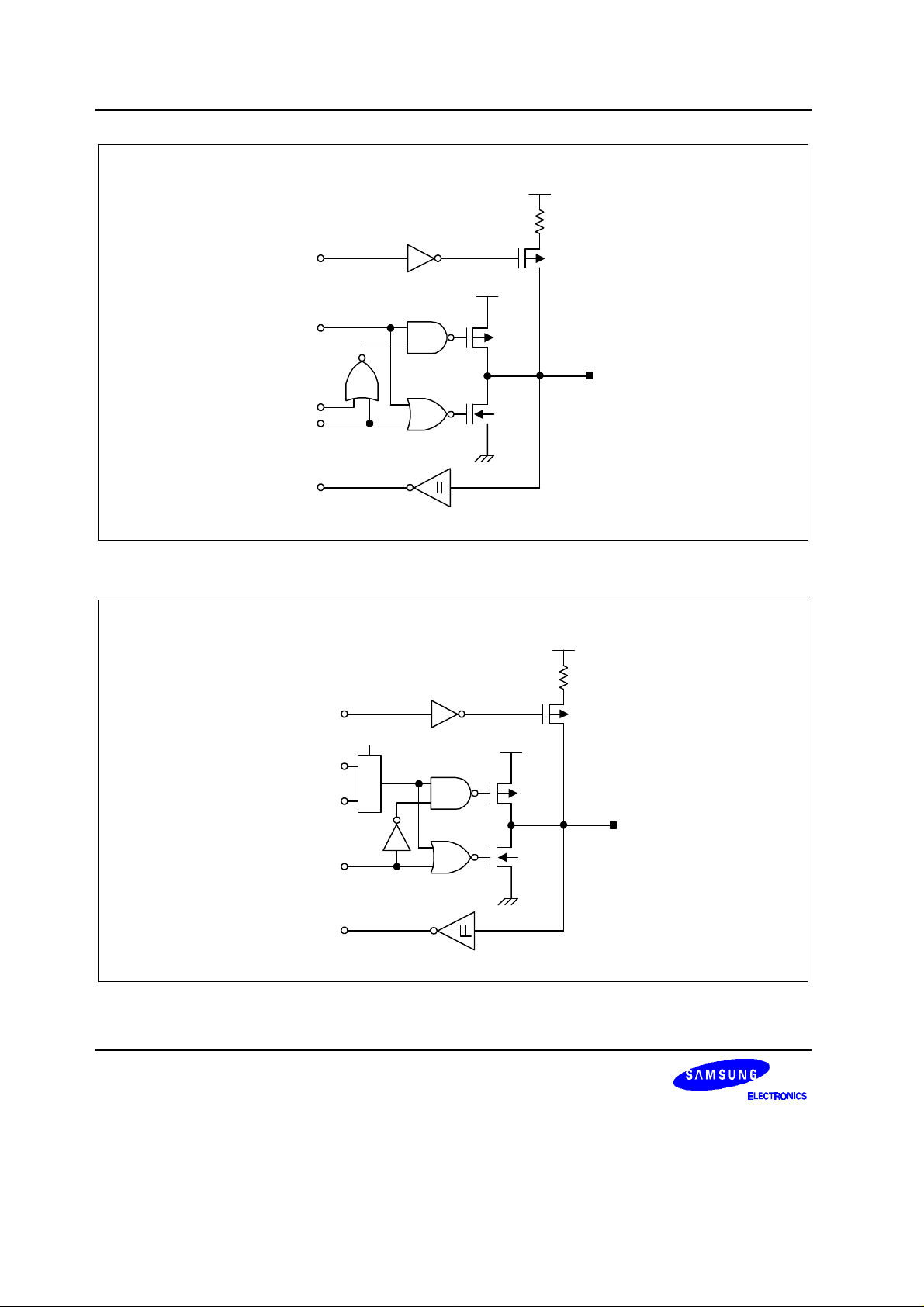
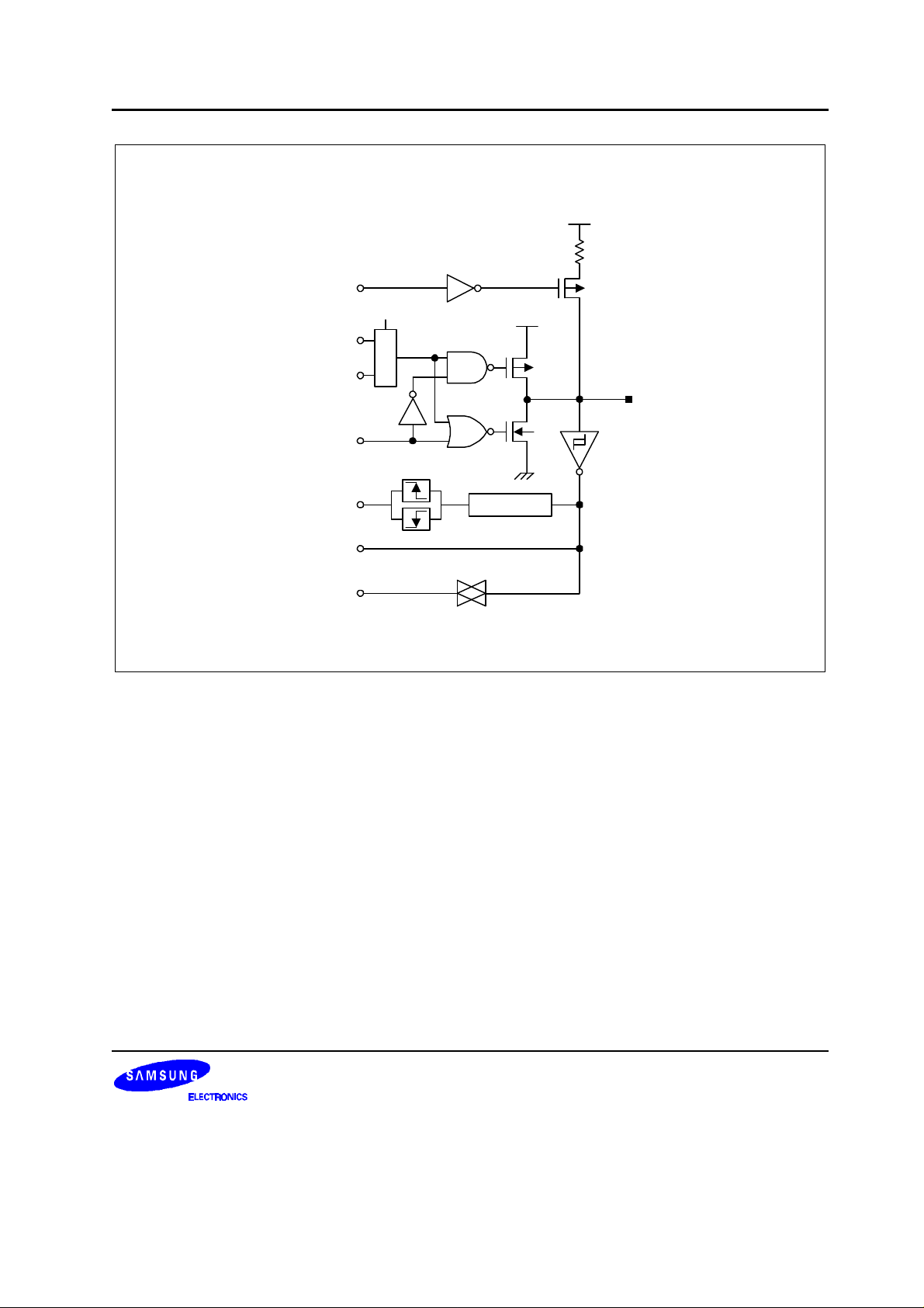
PRODUCT OVERVIEW KS88C4616/C4632/P4632
V
DD
Pull-up Resistor
(Typical Value: 47 KΩ)
Pull-up
Enable
V
DD
Data
In/Out
Open-drain
Output DIsable
In
Figure 1-4. Pin Circuit Type 1 (Port 0,1 and Port 6)
Pull-up
Enable
Port 2 (Low Byte) Data
External Interface
(AS, DS, R/W, DM)
Output DIsable
Figure 1-5. Pin Circuit Type 2 (Port 2, P2.0–P2.3 only)
V
DD
Pull-up Resistor
(Typical Value: 47 KΩ)
Select
M
Data
V
DD
U
X
In/Out
In
1-10
KS88C4616/C4632/P4632 PRODUCT OVERVIEW
V
DD
Pull-up Resistor
(Typical Value: 47 KΩ)
Pull-up
Enable
Port 2 (High Byte) Data
Select
M
V
DD
U
Control Output (BUZ)
X
In/Out
Output DIsable
External
Interrupt Input
Noise Filter
Normal
Input
ZCD Input
Figure 1-6. Pin Circuit Type 3 (Port 2, P2.4–P2.7 only)
1-11
 Loading...