

Samsung KS88C4404 Datasheet

KS88C4404 MICROCONTROLLER PRODUCT OVERVIEW
1PRODUCT OVERVIEW
SAM8 PRODUCT FAMILY
Samsung's new SAM8 family of 8-bit single-chip CMOS microcontrollers offers a fast and efficient CPU, a wide
range of integrated peripherals, and various mask-programmable ROM sizes.
A dual address/data bus architecture and a large number of bit- or nibble-configurable I/O ports provide a flexible
programming environment for applications with varied memory and I/O requirements.
Timer/counters with selectable operating modes are included to support real-time operations. Many SAM8
microcontrollers have an external interface that provides access to external memory and other peripheral devices.
The sophisticated interrupt structure recognizes up to eight interrupt levels. Each level can have one or more
interrupt sources and vectors. Fast interrupt processing (within a minimum six CPU clocks) can be assigned to
specific interrupt levels.
KS88C4404 MICROCONTROLLER
The KS88C4404 single-chip microcontroller is fabricated using a highly advanced CMOS process. Its design is
based on the powerful SAM8 CPU core. Stop and Idle power-down modes were implemented to reduce power
consumption. The size of the internal register file is logically expanded, increasing the addressable on-chip
register space to 1040 bytes. A flexible yet sophisticated external interface is used to access up to 64-Kbytes of
program and data memory. The KS88C4404 is a versatile microcontroller that is ideal for use in a wide range of
general-purpose applications such as CD-ROM/DVD-ROM drives.
Using the SAM8 modular design approach, the following peripherals were integrated with the SAM8 CPU core:
1–1

PRODUCT OVERVIEW KS88C4404 MICROCONTROLLER
— Six configurable 8-bit general I/O ports
— One 8-bit n-channel, open-drain output port
— One 8-bit input port for A/D converter input or
digital input
— Full-duplex serial data port with one
synchronous and three asynchronous (UART)
operating modes
— Two 8-bit timers with interval timer or PWM
mode
— Two 16-bit timer/counters with four
programmable operating modes
— Two programmable 8-bit PWM modules with
corresponding output pins
— One 8-bit capture module with CAP input pin
— A/D converter with 8 selectable input pins
The KS88C4404 is a versatile microcontroller that is
ideal for use in a wide range of general-purpose
ROM-less applications such as CD-ROM/DVD-ROM
drivers.
Figure 1–1. KS88C4404 Microcontroller
1–2

KS88C4404 MICROCONTROLLER PRODUCT OVERVIEW
FEATURES
CPU
• SAM8 CPU core
Memory
• 1040-byte of internal register file
• 4-kbyte internal program memory area
External Interface
• 64-Kbyte external data memory area
• 64-Kbyte external program memory (ROMless)
• 60-Kbyte external program memory (normal)
Instruction Set
• 78 instructions
• IDLE and STOP instructions
Instruction Execution Time
• 240 ns at 25 MHz f
Interrupts
• 20 interrupt sources and 19 interrupt vectors
• Seven interrupt levels
• Fast interrupt processing (level0 and 3-7 only)
(minimum)
OSC
General I/O
• Six 8-bit general I/O ports (ports 0,1,2,3,4, and
5)
• One 8-bit n-channel, open-drain output port
(port 6)
• One 8-bit input port (for ADC input or port 7
digital input)
Serial Port
• Full-duplex serial data port (UART)
• Four programmable operating modes
PWM and Capture
• Two output channels (PWM0, PWM1)
• 8-bit resolution with 2-bit prescaler
• 97.66-kHz frequency (25-MHz CPU clock)
• Capture module with CAP input pin
Analog-to-Digital Converter
• Eight analog input pins
• 8-bit conversion resolution
• 7.68-µs conversion speed (25-MHz CPU clock)
Operating Temperature Range
• – 20°C to + 85°C
Timer/Counters
• Two 8-bit timers with interval timer or PWM
mode (timers A and B)
• Two 16-bit timer/counters with four
programmable operating modes (timers C and
D)
Operating Voltage Range
• 4.5 V to 5.5 V
Package Type
• 80-pin QFP, 80–pin TQFP
1–3
PRODUCT OVERVIEW KS88C4404 MICROCONTROLLER
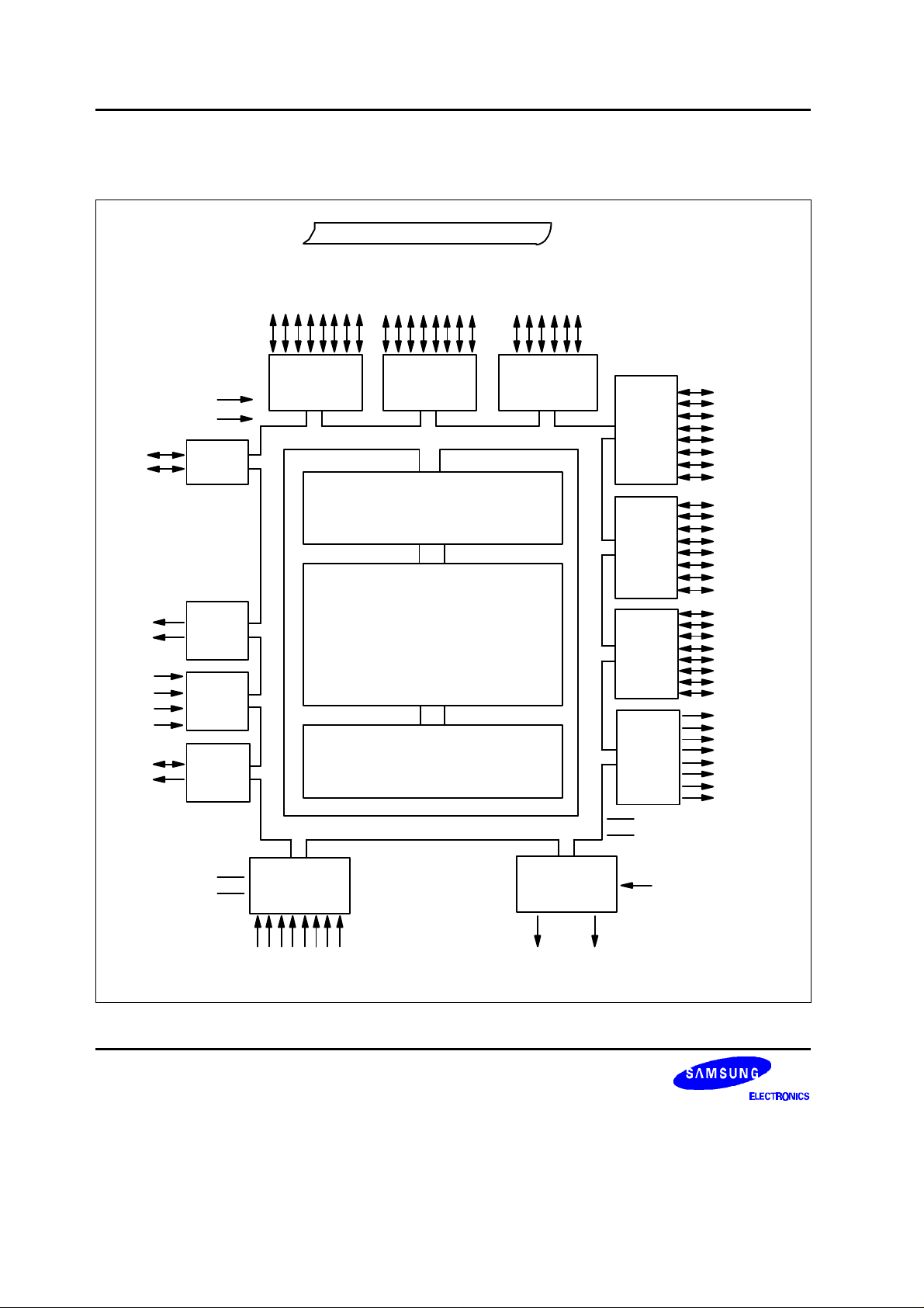
BLOCK DIAGRAM
EXTERNAL ADDRESS/DATA BUS
P2.6
P2.7
TA
TB
TCCK
TDCK
TCG
TDG
RxD
TxD
RESET
EA
PORT2
TIMERS
A and B
TIMERS
C and D
SERIAL
PORT
P0.0–P0.7
(A8–A15)
PORT 0
P1.0–P1.7
(AD0–AD7)
PORT 1 PORT 2
SAM8 BUS
PORT I/O & INTERRUPT
CONTROL
SAM8 CPU
1040-BYTE
REGISTER FILE
P2.0–P2.5
(Control Signal)
PORT 3
PORT 4
PORT 5
PORT 6 P6.0–P6.7
P3.0–P3.7
P4.0–P4.7
P5.0–P5.3
P5.4–P5.7
1–4
SS
AV
AVREF
A/D
CONVERTER
ADC0 /P7.0 –
ADC7 /P7.7
Figure 1–2. KS88C4404 Block Diagram
SAM8 BUS
PWM
MODULE
PWM0 PWM1
VDD1
SS1
,V
DD2
V
,VSS2
CAPTURE (P3.6)

KS88C4404 MICROCONTROLLER PRODUCT OVERVIEW
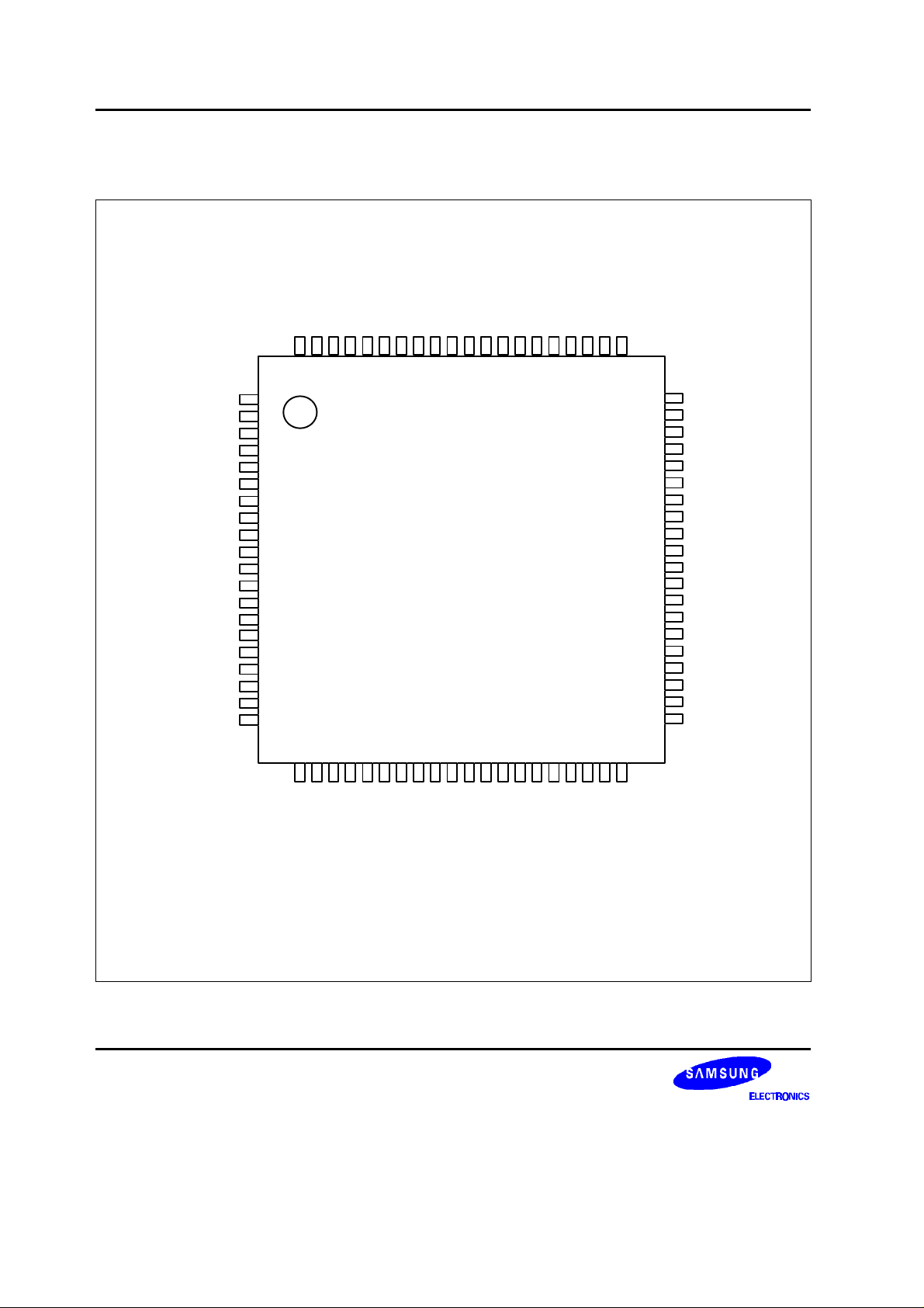
PIN ASSIGNMENTS
P1.7 / AD7
P1.6 / AD6
P1.5 / AD5
P1.4 / AD4
P1.3 / AD3
P1.2 / AD2
P1.1 / AD1
P1.0 / AD0
V
P0.7 / A15
P0.6 / A14
P0.5 / A13
P0.4 / A12
P0.3 / A11
P0.2 / A10
78
79
80
77
76
75
DD1
(int.)
74
73
72
71
70
69
68
67
66
EA
65
P0.1 / A9
P0.0 / A8
P5.7
P5.6
P5.5
P5.4
P5.3
P5.2
P5.1
P5.0
VDD2 (ext.)
P2.7 / TB
P2.6 / TA
P2.5 / PM
P2.4 / MR
P2.3 / DM
P2.2 / MW
P2.1 / DS
P2.0 / AS
RxD
TxD
PWM1
PWM0
P3.0 / TCCK / INT0
1
2
3
4
5
6
7
8
9
10
11
12
13
14
15
16
17
18
19
20
21
22
23
24
25
26
27
KS88C4404
80-QFP
(TOP VIEW)
31
30
29
28
32
33
34
35
36
37
38
39
40
64
63
62
61
60
59
58
57
56
55
54
53
52
51
50
49
48
47
46
45
44
43
42
41
RESET
NC
AS
VSS1 (int.)
XOUT
IN
X
P6.0
P6.1
P6.2
P6.3
P6.4
P6.5
P6.6
P6.7
P7.7 / ADC7
P7.6 / ADC6
P7.5 / ADC5
P7.4 / ADC4
P7.3 / ADC3
AVSS
P7.2 / ADC2
P7.1 / ADC1
AVREF
P7.0 / ADC0
P3.1 / TDCK / INT1
WAIT
SS2
(ext.)
P4.5 / INT9
P4.4 / INT8
P4.3 / INT7
P4.2 / INT6
P4.1 / INT5
P4.0 / INT4
V
P3.7 /
P3.6 / CAP
P3.5
P3.4
P3.3 / TDG / INT3
P3.2 / TCG / INT2
Figure 1–3. KS88C4404 Pin Assignments
P4.7 / INT11
P4.6 / INT10
1–5
PRODUCT OVERVIEW KS88C4404 MICROCONTROLLER
PIN ASSIGNMENTS (Continued)
P1.7 / AD7
P1.6 / AD6
P1.5 / AD5
P1.4 / AD4
P1.3 / AD3
P1.2 / AD2
P1.1 / AD1
P1.0 / AD0
V
P0.7 / A15
P0.6 / A14
P0.5 / A13
P0.4 / A12
P0.3 / A11
P0.0 / A8
V
(ext.
DD2
P2.7 / TB
P2.6 / TA
P5.7
P5.6
P5.5
P5.4
P5.3
P5.2
P5.1
P5.0
PM
MR
DM
MW
DS
AS
RxD
TxD
P0.2 / A10
P0.1 / A9
76
77
78
79
80
1
2
3
4
5
6
7
8
9
10
)
11
12
13
14
15
16
17
18
19
20
25
24
23
22
21
DD1
(int.)
72
73
74
75
KS88C4404
80-TQFP
(TOP VIEW)
29
28
27
26
71
30
70
31
69
32
68
33
67
34
66
35
65
36
EA
64
37
63
38
RESET
AS
NC
61
62
Vss1 (int.)
60
X
OUT
X
IN
P6.0
P6.1
P6.2
P6.3
P6.4
P6.5
P6.6
P6.7
P7.7 / ADC7
P7.6 / ADC6
P7.5 / ADC5
P7.4 / ADC4
P7.3 / ADC3
AV
SS
P7.2 / ADC2
P7.1 / ADC1
AV
REF
39
59
58
57
56
55
54
53
52
51
50
49
48
47
46
45
44
43
42
41
40
1–6
P4.3 / INT7
P4.2 / INT6
P4.1 / INT5
P4.0 / INT4
VSS2 (ext.)
P3.7 / WAIT
P3.6 / CAP
P3.5
P3.4
P3.3 / TDG / INT3
P3.2 / TCG / INT2
P3.1 / TDCK / INT1
P3.0 / TCCK / INT0
PWM0
PWM1
Figure 1–4. KS88C4404 Pin Assignments
P4.7 / INT11
P4.6 / INT10
P4.5 / INT9
P4.4 / INT8
P7.0 / ADC0

KS88C4404 MICROCONTROLLER PRODUCT OVERVIEW
PIN DESCRIPTIONS
Table 1–1. KS88C4404 Pin Descriptions
Pin
Name
Pin
Type
Pin
Description
P0.0 - P0.7 I/O Nibble programmable port; input or output mode
selected by software; Schmitt trigger input or pushpull, open-drain output with software assignable
pull-ups; alternately configurable as external
interface address lines A8 - A15.
P1.0 - P1.7 I/O Same general characteristics as port 0; alternately
configurable as external interface address/data lines
AD0 - AD7.
P2.0 - P2.7 I/O General I/O port with Schmitt trigger input or push-
pull output. bit programmable;
P2.0 / Address Strobe (AS)
P2.1 / Data Strobe (DS)
P2.2 / Memory Write (MW)
P2.3 / Data Memory select (DM)
P2.4 / Memory Read (MR)
P2.5 / Program Memory select (PM)
P2.6 / timer A output (TA)
P2.7 / timer B output (TB)
P3.0 - P3.7 I/O General I/O port with bit programmable pins.
Schmitt trigger input or push-pull output with
software assignable pull-ups. Input or output mode
is selectable by software. P3.0 - P3.3 are alternately
used as inputs for external interrupts INT0-INT3,
respectively (with noise filters and interrupt control):
P3.0 / timer C clock input (TCCK) / INT0
P3.1 / timer D clock input (TDCK) / INT1
P3.2 / timer C gate input (TCG) / INT2
P3.3 / timer D gate input (TDG) / INT3
P3.6 / Capture data input (CAP)
P3.7 / for slow memory interface
P4.0 - P4.7 I/O General I/O port with bit programmable pins.
Schmitt trigger input or push-pull, open-drain output
with software assignable pull-ups. Input or output
mode is selectable by software. P4.0-P4.7 can
alternately be used as inputs for external interrupts
INT4-INT11, respectively (with noise filters and
interrupt control)
Circuit
Type
3 2, 1,
QFP Pin
Number
Share
A8 - A15
80-75
3 73-66 AD0 - AD7
5 19 - 12
AS, DS, MW,
DM, MR,
PM, TA, TB
4 24-31 (See pin
description)
4 33-40 INT4 -
INT11
Pins
1–7
PRODUCT OVERVIEW KS88C4404 MICROCONTROLLER
Table 1–1. KS88C4404 Pin Descriptions (Continued)
Pin
Name
P5.0–P5.7
P6.0–P6.7
ADC0–ADC7
AV
, AV
REF
SS
RxD
TxD
PWM0,
PWM1
TA, TB
INT0–INT11
TCCK, TDCK
TCG, TDG
CAP
WAIT
RESET
EA
V
, V
DD1
SS1
V
, V
DD2
SS2
XIN, X
OUT
AS
NC
Pin
Type
I/O
General I/O port with nibble programmable
Pin
Description
Circuit
Type
QFP Pin
Number
3 10–3 —
pins. Schmitt trigger input or push-pull,
open-drain output mode. Mode and pull-ups
are assigned by software.
O
N-channel, open-drain output port; the pin
8 58–51 —
circuits can withstand loads up to 9 volts.
I
Analog input pins for A/D converter module.
Alternatively used as general-purpose
2 41, 43–44,
46–50
P7.0–P7.7
digital input port 7.
—
I/O
A/D converter reference voltage and ground
Serial data RxD pin for receive input and
— 42, 45 —
6 20 —
transmit output (mode 0)
O
Serial data TxD pin for transmit output and
7 21 —
shift clock input (mode 0)
O
Pulse width modulation output pins
O
Output pins for timer A and timer B
I
External interrupt input pins
I
External clock input for timer C and timer D
I
Gate input pins for timer C and timer D
I
Capture data input for PWM module
I
Input pin for the slow memory timing signal
7 23, 22 —
5 13, 12 P2.6, P2.7
4 24–27,
33–40
P3.0–P3.3,
P4.0–P4.7
4 24, 25 P3.0, P3.1
4 26, 27 P3.2, P3.3
4 30 P3.6
4 31 P3.7
from the external interface
I
System reset pin (pull-up resistor: 220 kΩ)
I
External access (EA) pin with two modes:
1 64 —
— 65 —
5 V input: normal ROM-less operation with
external interface (0 V is not allowed)
9 V–10 V input: for factory test mode
—
Power input pins for CPU operation
— 74, 61 —
(internal)
—
Power input pins for port output (external)
—
Main oscillator pins
O
Address strobe
— 11, 32 —
— 59, 60 —
7 62 —
— No connection pins (connect to VSS) — 62, 63 —
Share
Pins
NOTE VDD1 must be connected to VDD2 in users application circuit, VSS1 & VSS2 also.
1–8

KS88C4404 MICROCONTROLLER PRODUCT OVERVIEW
PIN CIRCUITS
Table 1–2. Pin Circuit Assignments for the KS88C4404
Circuit Number Circuit Type KS88C4404 Assignments
1 Input
2 Input
3 I/O
4 I/O
5 I/O
6 I/O
7 Output
8 Output
RESET pin
A/D converter input pins, ADC0–ADC7
Port 0, 1, and 5
Ports 3 and 4, TCCK, TDCK, TCG, TDG, CAP, WAIT, INT0–INT11
Port 2 (AS, DS, MW, DM, MR, PM, TA,TB)
Serial port RxD pin
Serial port TxD pin, PWM0, PWM1 and AS
Port 6 (n-channel, open-drain output with high current capability)
1–9
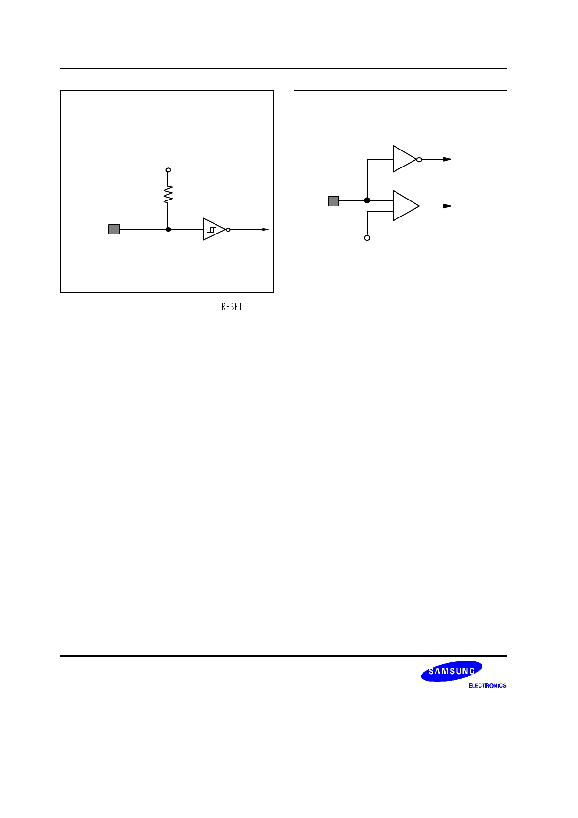
PRODUCT OVERVIEW KS88C4404 MICROCONTROLLER
V
DD
PULL-UP
RESISTOR
(Typical 230 kΩ)
INPUT
Figure 1–5. Pin Circuit Type 1 ( )
INPUT
BUFFER
IN
V
+
–
REF
ADC
LOGIC
Figure 1–6. Pin Circuit Type 2 (ADC0–ADC7)
1–10

KS88C4404 MICROCONTROLLER PRODUCT OVERVIEW
V
DD
PULL-UP
RESISTOR
(Ty pical 46 kΩ)
PULL-UP
ENABLE
DATA
OPENDRAIN
OUTPUT
DISABLE
INPUT
V
DD
IN / OUT
V
SS
Figure 1–7. Pin Circuit Type 3 (Ports 0,1, and 5)
1–11
 Loading...