

Samsung KS88P2416, KS88C2432, KS88P2432, KS88C2416 Datasheet

KS88C2416/P2416/C2432/P2432 PRODUCT OVERVIEW
1 PRODUCT OVERVIEW
KS88-SERIES MICROCONTROLLERS
Samsung's KS88 series of 8-bit single-chip CMOS microcontrollers offers a fast and efficient CPU, a wide range of
integrated peripherals, and various mask-programmable ROM sizes. Among the major CPU features are:
— Efficient register-oriented architecture
— Selectable CPU clock sources
— Idle and Stop power-down mode release by interrupt
— Built-in basic timer with watchdog function
A sophisticated interrupt structure recognizes up to eight interrupt levels. Each level can have one or more
interrupt sources and vectors. Fast interrupt processing (within a minimum of four CPU clocks) can be assigned to
specific interrupt levels.
KS88C2416/P2416/C2432/P2432 MICROCONTROLLER
The KS88C2416/P2416/C2432/P2432 single-chip
CMOS microcontroller are fabricated using the highly
advanced CMOS process, based on Samsung’s
newest CPU architecture.
The KS88C2416 is a microcontroller with a 16-Kbyte
mask-programmable ROM embedded.
The KS88C2432 is a microcontroller with a 32-Kbyte
mask-programmable ROM embedded.
The KS88P2416 is a microcontroller with a 16-Kbyte
one-time-programmable ROM embedded.
The KS88P2432 is a microcontroller with a 32-Kbyte
one-time-programmable ROM embedded.
Using a proven modular design approach, Samsung
engineers have successfully developed the
KS88 C2416/P2416/C2432/P2432 by integrating the
following peripheral modules with the powerful SAM8
core:
— Six programmable I/O ports, including five 8-bit
ports and one 5-bit port, for a total of 45 pins.
— Eight bit-programmable pins for external
interrupts.
— One 8-bit basic timer for oscillation stabilization
and watchdog functions (system reset).
— Two 8-bit timer/counter and two 16-bit
timer/counter with selectable operating modes.
— Watch timer for real time.
— 8-input A/D converter
— Serial I/O interface
The KS88C2416/P2416/C2432/P2432 is versatile
microcontroller for camera, LCD and ADC
application, etc. They are currently available in 80-pin
TQFP and 80-pin QFP package
OTP
The KS88P2416/P2432 are OTP (One Time Programmable) version of the KS88C2416/C2432 microcontroller.
The KS88P2416 microcontroller has an on-chip 16-Kbyte one-time-programmable EPROM instead of a masked
ROM. The KS88P2432 microcontroller has an on-chip 32-Kbyte one-time-programmable EPROM instead of a
masked ROM. The KS88P2416 is comparable to the KS88C2416, both in function and in pin configuration.
The KS88P2432 is comparable to the KS88C2432, both in function and in pin configuration.
1-1

PRODUCT OVERVIEW KS88C2416/P2416/C2432/P2432
FEATURES
Memory
• ROM: 32-Kbyte (KS88C2432/P2432)
• ROM: 16-Kbyte (KS88C2416/P2416)
• RAM: 1056-Byte (KS88C2432/P2432,
KS88C2424/P2424)
• RAM: 544-Byte (KS88C2416/P2416,
KS88C2408/P2408)
• Data memory mapped I/O
Oscillation Sources
• Crystal, ceramic, RC (main)
• Crystal for subsystem clock
• Main system clock frequency 1-10 MHz
(3 MHz at 1.8 V, 10 MHz at 2.7 V)
• Subsystem clock frequency: 32.768 kHz
• CPU clock divider (1/1, 1/2, 1/8, 1/16)
Two Power-Down Modes
• Idle (only CPU clock stops)
• Stop (System clock stops)
Interrupts
• 6 level 8 vector 8 internal interrupt
• 2 level 8 vector 8 external interrupt
45 I/O Pins
• 45 configurable I/O pins
Basic Timer
• Overflow signal makes a system reset.
• Watchdog function
8-Bit Timer/Counter A
• Programmable 8-bit timer
• Interval, capture, PWM mode
• Match/capture, overflow interrupt
8-Bit Timer/Counter B
• Programmable 8-bit timer
• Carrier frequency generator
16-Bit Timer/Counter 0
• Programmable 16-bit timer
• Match interrupt generates
16-Bit Timer/Counter 1
• Programmable 16-bit timer
• Interval, capture, PWM mode
• Match/capture, overflow interrupt
Watch Timer
• Real-time and interval time measurement
• Clock generation for LCD
• Four frequency outputs for buzzer sound
LCD Controller/Driver
• Maximum 16-digit LCD direct drive capability
• Display modes: static, 1/2 duty (1/2 bias)
• 1/3 duty (1/2 or 1/3 bias), 1/4 duty (1/3 bias)
A/D Converter
• Eight analog input channels
• 50 µs conversion speed at 1 MHz f
ADC
clock
• 10-bit conversion resolution
8-Bit Serial I/O Interface
• 8-bit transmit/receive mode
• 8-bit receive mode
• LSB-first/MSB-first transmission selectable
• Internal/external clock source
Voltage Booster
• LCD display voltage supply
• S/W control en/disable
• 3.0 V drive
Voltage Detector
• Programmable detection voltage
(2.2 V, 2.4 V, 3.0 V, 4.0 V)
• En/Disable S/W selectable
Instruction Execution Times
• 400 ns at 10 MHz (main)
• 122 us at 32.768 kHz (subsystem)
Operating Temperature Range
• -40 °C to 85 °C
Operating Voltage Range
• 1.8 V to 5.5 V
Package Type
• 80-pin QFP
• 80-pin TQFP
KS88C2432’s ROM version device
• KS88C2424 (ROM 24 Kbyte)
KS88C2416’s ROM version device
• KS88C2408 (ROM 8 Kbyte)
1-2

KS88C2416/P2416/C2432/P2432 PRODUCT OVERVIEW
BLOCK DIAGRAM
X
XT
IN
TAOUT/TAPWM/P3.1
TACLK/P3.2
TACAP/P3.3
TBPWM/P3.0
T1CAP/P1.0
T1CLK/P1.1
T1OUT/T1PWM/P1.2
P0.0-P0.7/
INT0-INT7
8-Bit
Timer/
Counter A
8-Bit
Timer/
Counter B
16-Bit
Timer/
Counter 0
16-Bit
Timer/
Counter 1
I/O Port 0
RESET
IN
X
OUT XTOUT
OSC/
RESET
Basic
Timer
I/O Port and Interrupt Control
BUZ/P1.4
Watch
Timer
Voltage
Detector
Voltage
Booster
LCD
Driver
V
VLDREF
CB
CA
VLC0-VLC2
COM0-COM3
SEG0-SEG15
SEG16-SEG31
P1.0-P1.7
AV
REF
AV
SS
P2.0-P2.7/
ADC0-ADC7
P3.0-P3.4
I/O Port 1
A/D
Converter
I/O Port 2
I/O Port 3
SAM88 RC CPU
544/1056 Byte
Register File
16/32-Kbyte
ROM
Figure 1-1. KS88C2416/2432 Block Diagram
Serial I/O
Port
I/O Port 4
I/O Port 5
SI/P1.7
SO/P1.5
SCK/P1.6
P4.0-P4.7
P5.0-P5.7
1-3
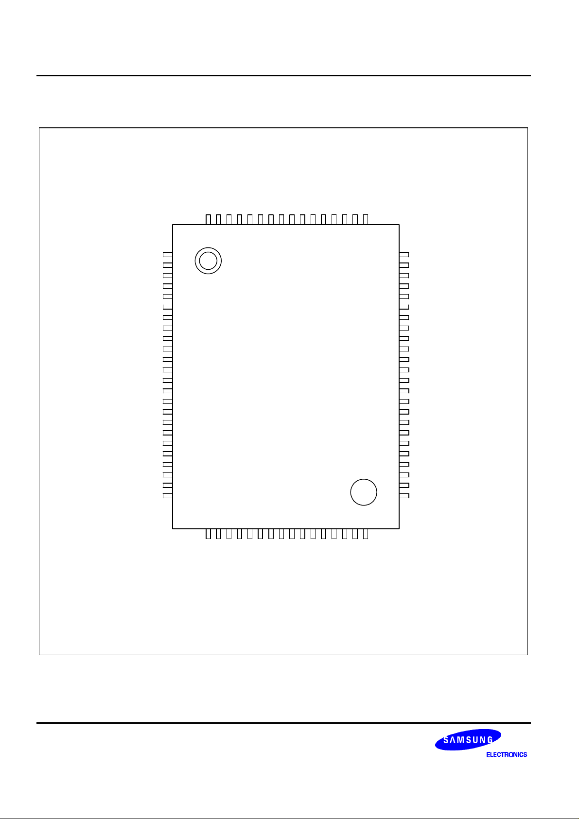
PRODUCT OVERVIEW KS88C2416/P2416/C2432/P2432
P1.2/T1OUT/T1PWM
PIN ASSIGNMENT
SEG25/P5.1
SEG24/P5.0
SEG23/P4.7
SEG22/P4.6
SEG21/P4.5
SEG20/P4.4
SEG19/P4.3
SEG18/P4.2
SEG17/P4.1
SEG16/P4.0
SEG15
SEG14
SEG13
SEG12
SEG11
SEG10
SEG26/P5.2
SEG27/P5.3
SEG28/P5.4
SEG29/P5.5
SEG30/P5.6
SEG31/P5.7
P3.0/TBPWM
P3.1/TAOUT/TAPWM
P3.2/TACLK
P3.3/TACAP/SDAT
P3.4/SCLK
V
DD
V
SS
X
OUT
X
TEST
XT
XT
OUT
RESET
P0.0/INT0
P0.1/INT1
P0.2/INT2
P0.3/INT3
P0.4/INT4
807978777675747372717069686766
1
2
3
4
5
6
7
8
9
10
11
12
13
14
15
IN
KS88C2416/P2416/
C2432/P2432
(80-QFP-1420C)
16
17
IN
18
19
20
21
22
23
24
65
64
63
62
61
60
59
58
57
56
55
54
53
52
51
50
49
48
47
46
45
44
43
42
41
SEG9
SEG8
SEG7
SEG6
SEG5
SEG4
SEG3
SEG2
SEG1
SEG0
COM3
COM2
COM1
COM0
VLC2
VLC1
VLC0
CA
CB
AV
SS
AV
REF
P2.7/ADC7/V
P2.6/ADC6
P2.5/ADC5
VLDREF
1-4
252627282930313233343536373839
40
P1.3
P1.7/SI
P1.5/SO
P1.4/BUZ
P0.5/INT5
P0.6/INT6
P0.7/INT7
P1.0/T1CAP
P1.1/T1CLK
P1.6/SCK
P2.0/ADC0
P2.1/ADC1
P2.2/ADC2
P2.3/ADC3
P2.4/ADC4
Figure 1-2. KS88C2416/2432 Pin Assignment (80-QFP)
KS88C2416/P2416/C2432/P2432 PRODUCT OVERVIEW
PIN DESCRIPTIONS
Table 1-1. KS88C2416/2432 Pin Descriptions
Pin
Names
P0.0–P0.7 I/O I/O port with bit programmable pins;
Pin
Type
Pin
Description
Circuit
Type
Pin
Numbers
(note)
Share
Pins
D–4 20–27 INT0–INT7
Schmitt trigger input or output mode
selected by software; software assignable
pull-up. P0.0–P0.7 can be used as inputs
for external interrupts INT0–INT7
(with noise filter and interrupt control).
P1.0–1.7 I/O I/O port with bit programmable pins; Input
or output mode selected by software;
Open-drain output mode can be selected
by software; software assignable pull-up.
Alternately P1.0–P1.7 can be used as SI,
SO, SCK, BUZ, T1CAP, T1CLK, T1OUT,
E–2 28-35 SI, SO, SCK,
BUZ, T1CAP
T1CLK
T1OUT
T1PWM
T1PWM
P2.0–P2.7 I/O I/O port with bit programmable pins;
normal input and AD input or output mode
selected by software; software assignable
pull-up.
P3.0–P3.4 I/O I/O port with bit programmable pins. Input
or push-pull output with software
assignable pull-up. Alternately P3.0–P3.3
can be used as TACAP, TACLK, TAOUT,
TAPWM, TBPWM
F–10
F–18
36–42,
43
ADC0–ADC6
V
VLDREF
(ADC7)
D–2 7–11 TACAP
TACLK
TAOUT
TAPWM
TBPWM
P4.0–P4.7 I/O I/O port with bit programmable pins.
H–14 71–78 SEG16–SEG23
Push-pull or open drain output and input
with software assignable pull-up.
P4.0–P4.7 can alternately be used as
outputs for LCD SEG
P5.0–P5.7 I/O Have the same characteristic as port 4 H–14 79–6 SEG24–SEG31
1-5

PRODUCT OVERVIEW KS88C2416/P2416/C2432/P2432
Table 1-1. KS88C2416/2432 Pin Descriptions (Continued)
Pin
Names
ADC0–ADC6
ADC7
AV
REF
AV
SS
Pin
Type
I A/D converter analog input channels F–10
Pin
Description
Circuit
Type
F–18
Pin
Numbers
36–42
43
(note)
P2.0–P2.6
– A/D converter reference voltage – 44 –
– A/D converter ground – 45 –
Share
Pins
P2.7
INT0–INT7 I External interrupt input pins D–4 20–27 P0.0–P0.7
RESET
I System reset pin
B 19 –
(pull-up resistor: 250 kΩ)
TEST I 0 V: Normal MCU operating
– 16 –
5 V: Test mode
12 V: for OTP writing
SDAT, SCLK O Serial OTP interface pins; serial data
D–2 10, 11 P3.3, P3.4
and clock
V
DD, VSS
– Power input pins for CPU operation
– 12, 13 –
(internal) and Power input for OTP
Writing
X
OUT, XIN
– Main oscillator pins – 14, 15 –
SCK, SO, SI I/O Serial I/O interface clock signal E–2 33–35 P1.5–P1.7
V
VLDREF
I Voltage detector reference voltage
F–18 43 P2.7
input
TACAP I Timer A Capture input D–2 10 P3.3
TACLK I Timer A External clock input D–2 9 P3.2
TAOUT/TAPWM O Timer A output and PWM output D–2 8 P3.1
TBPWM O Timer B PWM output D–2 7 P3.0
T1CAP I Timer 1 Capture input E–2 28 P1.0
T1CLK I Timer 1 External clock input E–2 29 P1.1
T1OUT/T1PWM O Timer 1 output and PWM output E–2 30 P1.2
COM0–COM3 O LCD common signal output H 51–54 –
SEG0–SEG15 O LCD segment output H 55–70 –
SEG16–SEG23 O LCD segment output H–14 71–78 P4.0–P4.7
SEG24–SEG31 O LCD Segment output H–14 79–6 P5.0–P5.7
V
LC0–VLC2
BUZ O 0.5, 1, 2 or 4 kHz frequency output for
O LCD power supply – 48–50 –
E–2 32 P1.4
buzzer sound with 4.19 MHz main
system clock or 32768 Hz subsystem
clock
CA, CB – Capacitor terminal for voltage booster – 46–47 –
1-6
KS88C2416/P2416/C2432/P2432 PRODUCT OVERVIEW
Disable
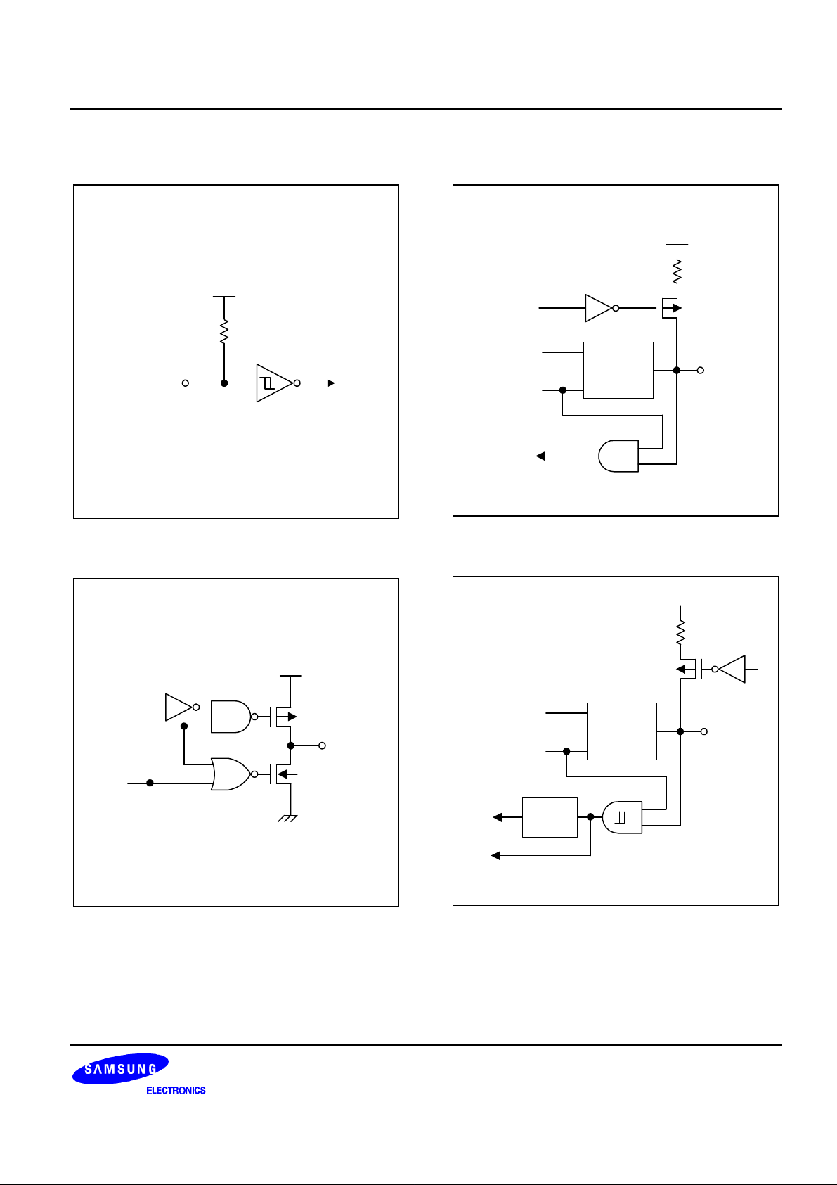
PIN CIRCUITS
DD
V
DD
V
Pull-up
Enable
P-Channel
In
Figure 1-3. Pin Circuit Type B (RESET)
V
DD
Data
Output
P-Channel
Out
N-Channel
Data
Output
Circuit
Type C
Disable
Figure 1-5. Pin Circuit Type D–2 (P3)
DD
V
DD
V
Data
Output
Disable
Pin Circuit
Type C
I/O
Pull-up
Enable
I/O
Figure 1-4. Pin Circuit Type C
Noise
Ext.INT
Filter
Input
Normal
Figure 1-6. Pin Circuit Type D–4 (P0)
1-7

PRODUCT OVERVIEW KS88C2416/P2416/C2432/P2432
V
DD
DD
V
Open drain
Enable
DD
V
Pull-up
Resistor
Pull-up
Enable
Data
Output
Disable
Schmitt Trigger
Figure 1-7. Pin Circuit Type E–2 (P1)
Pull-up
Enable
P-CH
N-CH
Data
Output
I/O
Disable
ADC & VLD
Enable
Data
VLD
REF
To ADC
Figure 1-9. Pin Circuit Type F–18 (P2.7/VLD
V
DD
V
LC0
V
LC1
Circuit
Type C
I/O
REF
)
Data
Output
Circuit
Type H-14
Disable
ADCEN
Data
To ADC
Figure 1-8. Pin Circuit Type F-10 (P2.0–P2.6)
1-8
I/O
SEG/
COM
V
LC2
Figure 1-10. Pin Circuit Type H (SEG/COM)
Out

KS88C2416/P2416/C2432/P2432 PRODUCT OVERVIEW
LC0
V
LC1
V
SEG
Output
Disable
LC2
V
Open Drain EN
Data
Figure 1-11. Pin Circuit Type H–4
V
DD
V
DD
Out
Pull-up
Enable
LCD Out EN
SEG
Output
Disable
Figure 1-12. Pin Circuit Type H–14 (P4, P5)
Circuit
Type H-14
1-9

KS88C2416/P2416/C2432/P2432 ELECTRICAL DATA
19 ELECTRICAL DATA
OVERVIEW
In this chapter, KS88C2416/C2432 electrical characteristics are presented in tables and graphs.
The information is arranged in the following order:
— Absolute maximum ratings
— Input/output capacitance
— D.C. electrical characteristics
— A.C. electrical characteristics
— Oscillation characteristics
— Oscillation stabilization time
— Data retention supply voltage in stop mode
— Serial I/O timing characteristics
— A/D converter electrical characteristics
19-1
 Loading...