

Samsung KS88P0716, KS88C0716 Datasheet

KS88C0716/P0716 PRODUCT OVERVIEW
1 PRODUCT OVERVIEW
SAM8 PRODUCT FAMILY
Samsung's SAM87 family of 8-bit single-chip CMOS microcontrollers offers a fast and efficient CPU, a wide
range of integrated peripherals, and various mask-programmable ROM sizes. Important CPU features include:
— Efficient register-oriented architecture
— Selectable CPU clock sources
— Idle and Stop power-down mode release by interrupt
— Built-in basic timer with watchdog function
A sophisticated interrupt structure recognizes up to eight interrupt levels. Each level can have one or more
interrupt sources and vectors. Fast interrupt processing (within a minimum of six CPU clocks) can be assigned to
specific interrupt levels.
KS88C0716/P0716 MICROCONTROLLERS
KS88C0716/P0716 single-chip 8-bit microcontrollers are based on the powerful SAM87 CPU architecture. The
internal register file is logically expanded to increase the on-chip register space. The KS88C0716 has 16-Kbyte
mask-programmable ROM. The KS88P0716 has 16-Kbyte one-time-programmable EPROM.
Following Samsung's modular design approach, the following peripherals are integrated with the SAM87 core:
— Seven programmable I/O ports (total 56 pins)
— One 8-bit basic timer for oscillation stabilization and watchdog functions
— One synchronous operating mode and three full-duplex asynchronous UART modes
— Two 8-bit timers with interval timer and PWM modes
— Two 16-bit general-purpose timer/counters
OTP
The KS88C0716 microcontroller is also available in OTP (One Time Programmable) version, KS88P0716.
KS88P0716 microcontroller has an on-chip 16-Kbyte one-time-programmable EPROM instead of masked ROM.
The KS88P0716 is comparable to KS88C0716, both in function and in pin configuration.
1-1

PRODUCT OVERVIEW KS88C0716/P0716
FEATURES
CPU
• SAM87 CPU core
Memory
• 272-byte general purpose register area
• 16-Kbyte internal program memory
• ROM-less operating mode
External Interface
• 64-Kbyte external data memory area
• 64-Kbyte external program memory area (ROMless mode)
Instruction Set
• 78instructions
• IDLE and STOP instructions for power-down
mode
Instruction Execution Time
• 500 ns at 12 MHz f
CPU
(Min.)
Interrupts
• 17 interrupt sources
• 17 interrupt vectors
• Eight interrupt levels
• Fast interrupt processing
General I/O
• Four nibble-programmable ports
• One bit-programmable port
• Two bit-programmable ports for external
interrupts
Timers
• Two 8-bit timers with interval timer and PWM
modes
Timer/Counters
• Two 16-bit general-purpose timer/counters
Basic Timer
• One 8-bit basic timer (BT) for oscillation
stabilization control and watch dog timer function.
Serial Port
• One synchronous operating mode and three fullduplex asynchronous UART modes
Operating Temperature Range
• – 40°C to + 85°C
Operating Voltage Range
• 2.7 V to 5.5 V
Package Types
• 64-pin SDIP, 64-pin QFP
1-2
KS88C0716/P0716 PRODUCT OVERVIEW
Table 1-1. Comparison Table
Feature KS88C0116 KS88C0716
Core SAM8 SAM87
ROM 16 K bytes Same
RAM 272 bytes Same
I/O 54 56 (add two pins)
Port 6 Open drain (9 V drive) Normal C-MOS output
I/O option None Same
Timer 8-bit back-up timer None
Timer A, B
— 8-bit
— Interval/PWM mode
Same
(some differ in interval mode,
see manual)
— Timer A match interrupt
Timer C, D
Same
— Gate function
— Timer/counter
Watchdog timer None Watchdog timer (with BT)
SIO UART
Same
— 8-bit/9-bit UART
— SIO
Interrupt
External × 12
Same
— P2.4–P2.7, P4.0–P4.7
Internal × 6
— Timer A, C, D, SI, SO, Back-up
Internal × 5
— Timer A, C, D, SI, SO
Power down Stop/idle Same
Oscillator Crystal, ceramic Same
CPU clock divider 1/2 1/1, 1/2, 1/8, 1/16
Execution time (Min.)
Operating frequency
0.6 µs at 20 MHz (f
Max. 20 MHz (f
CPU
= 10 MHz) 0.5 µs at 12 MHz (f
CPU
= 10 MHz)
Max. 12 MHz (at 4.5 V)
CPU
= 12 MHz)
(2)
Max. 4 MHz (at 2.7 V)
Operating voltage 4.5–5.5 V 2.7–5.5 V at 4 MHz
4.5–5.5 V at 12 MHz
OTP/MTP MTP OTP
Pin assignment – Different
Package 64SDIP/64QFP Same
Start address 0020h 0100h
P5CON, P6CON BANK0 BANK1
Interrupt pending bit clear Write "1" Write "0"
NOTES:
1. The KS88C0716 can replace the KS88C0116. Their functions are mostly the same, but there are some differences.
Table 1-1 shows the comparison of KS88C0716 and KS88C0116.
1-3
PRODUCT OVERVIEW KS88C0716/P0716
2. Operating frequency is maximum CPU clock; the maximum oscillation frequency is 22.1184 MHz.
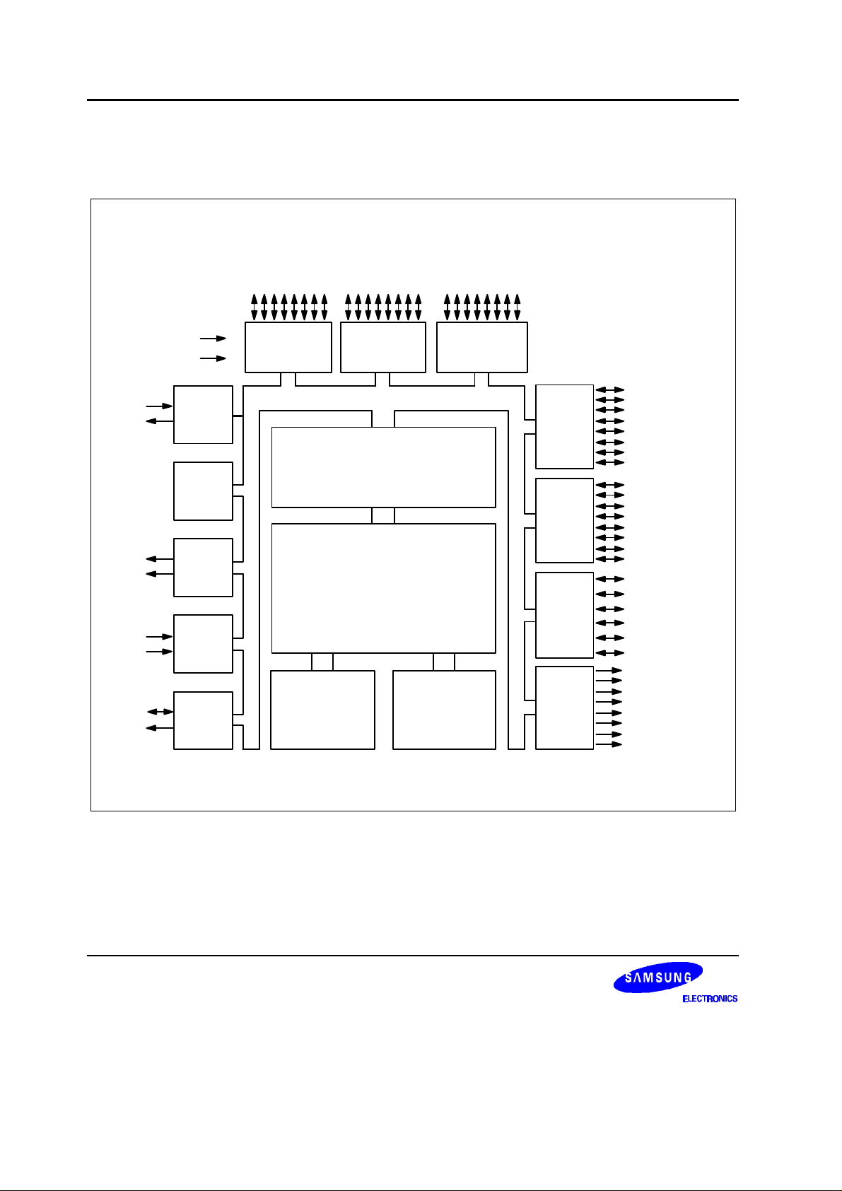
BLOCK DIAGRAM
X
X
OUT
TA
TB
TCCK
TDCK
P0.0–P0.7
(A8–A15)
RESET
EA
IN
MAIN
OSC
BASIC
TIMER
TIMERS
A and B
PORT 0
P1.0–P1.7
(AD0–AD7)
PORT 1
SAM87 BUS
PORT I/O and
INTERRUPT CONTROL
P2.0–P2.3,
P2.4/INT0–P2.7/INT3
PORT 2
PORT 3
PORT 4
P3.0–P3.7
P4.0/INT4 (TCG)
P4.1/INT5 (TDG)
P4.2/INT6–
P4.7/INT11
SAM87 CPU
PORT 5
TIMERS
C and D
P5.0–P5.3
P5.4–P5.7
1-4
RxD
TxD
SERIAL
PORT
16-KB ROM
272-BYTE
REGISTER FILE
Figure 1-1. KS88C0716 Block Diagram
PORT 6
P6.0–P6.7
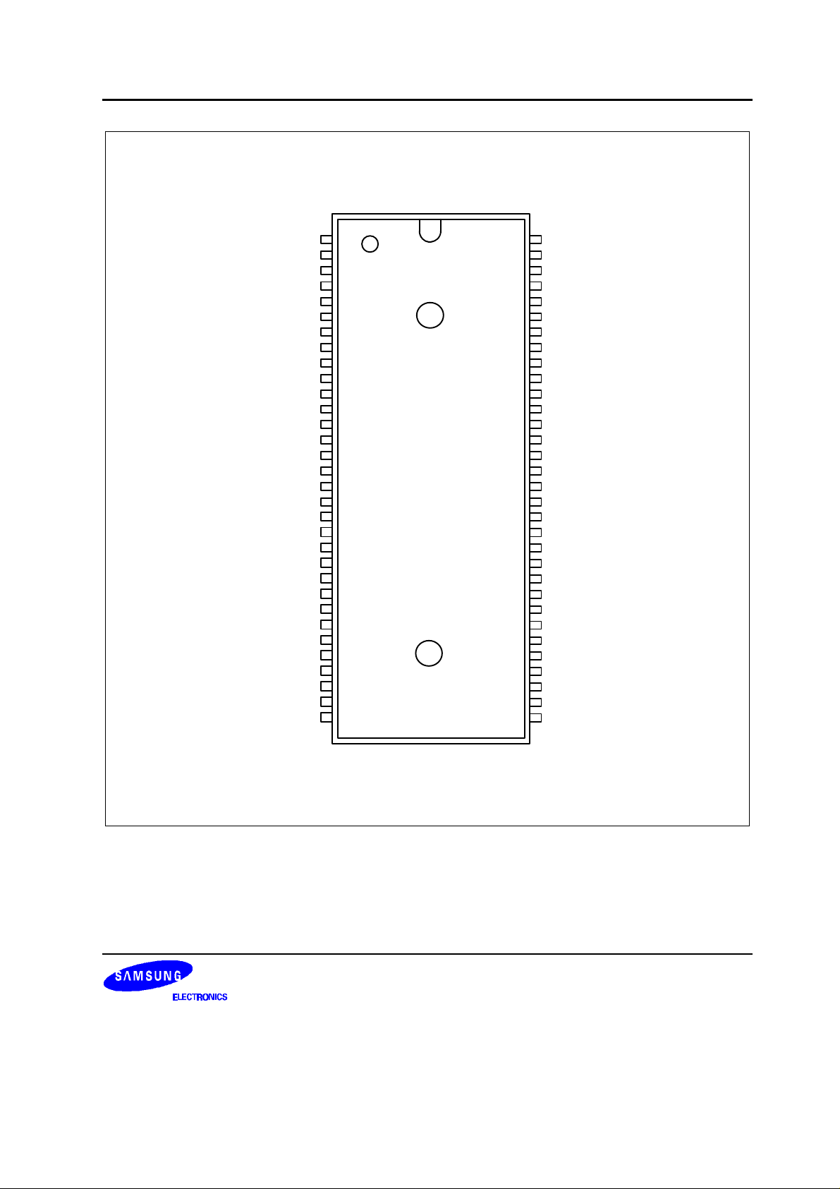
KS88C0716/P0716 PRODUCT OVERVIEW
64
63
62
61
60
59
58
57
56
55
54
53
52
51
50
49
48
47
46
45
44
43
42
41
40
39
38
37
36
35
34
33
P0.7/A15
P1.0/AD0
P1.1/AD1
P1.2/AD2
P1.3/AD3
P1.4/AD4
P1.5/AD5
P1.6/AD6
P1.7/AD7
P5.5
P5.4
P5.3
P5.2
P5.1
P5.0
V
DD2
V
SS2
AS
P2.0/
DS
P2.1/
W
P2.2/R/
DM
P2.3/
P2.4/INT0/
P2.5/INT1
P2.6/INT2
P2.7/INT3
P6.7
P6.6
P6.5
P6.4
P6.3
P6.2
P6.1
WAIT
P0.6/A14
P0.5/A13
P0.4/A12
P0.3/A11
P0.2/A10
P0.1/A9
P0.0/A8
P4.7/INT11
P4.6/INT10
P4.5/INT9
P4.4/INT8
P4.3/INT7
P4.2/INT6
P4.1/INT5/TDG
P4.0/INT4/TCG
V
DD1
V
SS1
X
OUT
X
EA
P5.6
P5.7
RESET
P3.7/RxD
P3.6/TxD
P3.5/TB
P3.4/TA
P3.3
P3.2
P3.1/TDCK
P3.0/TCCK
P6.0
1
2
3
4
5
6
7
8
9
10
11
12
13
14
15
16
17
18
19
IN
KS88C0716
64-SDIP
(Top View)
20
21
22
23
24
25
26
27
28
29
30
31
32
Figure 1-2. KS88C0716 Pin Assignments (64-SDIP)
1-5
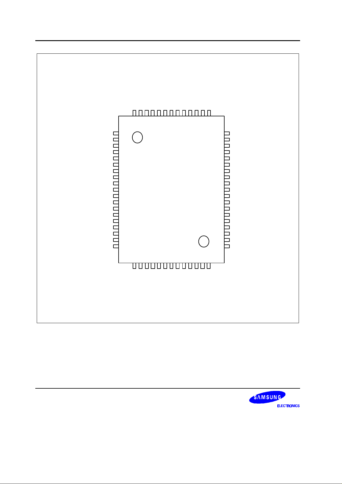
PRODUCT OVERVIEW KS88C0716/P0716
P1.4/AD4
P1.3/AD3
P1.2/AD2
P1.1/AD1
P1.0/AD0
P0.7/A15
P0.6/A14
P0.5/A13
P0.4/A12
P0.3/A11
P0.2/A10
P0.1/A9
P0.0/A8
52
53
54
55
56
57
58
59
60
61
62
63
64
51
50
49
48
47
46
45
44
43
42
41
40
39
38
37
36
35
34
33
P1.5/AD5
P1.6/AD6
P1.7/AD7
P5.5
P5.4
P5.3
P5.2
P5.1
P5.0
V
DD2
V
SS2
P2.0/AS
P2.1/DS
P2.2/R/W
P2.3/DM
P2.4/INT0/
P2.5/INT1
P2.6/INT2
P2.7/INT3
WAIT
P4.7/INT11
P4.6/INT10
P4.5/INT9
P4.4/INT8
P4.3/INT7
P4.2/INT6
P4.1/INT5/TDG
P4.0/INT4/TCG
V
DD1
V
SS1
X
OUT
XIN
EA
P5.6
P5.7
RESET
P3.7/RxD
P3.6/TxD
P3.5/TB
1
2
3
4
5
6
7
8
9
10
11
12
13
14
15
16
17
18
19
20
KS88C0716
23
22
21
64-QFP
(Top View)
28
27
26
25
24
29
30
31
32
1-6
P6.7
P6.6
P6.5
P6.4
P6.3
P6.2
P6.1
P6.0
P3.0/TCCK
P3.1/TDCK
P3.2
P3.3
P3.4/TA
Figure 1-3. KS88C0716 Pin Assignments (64-QFP)
KS88C0716/P0716 PRODUCT OVERVIEW
Table 1-2. KS88C0716 Pin Descriptions (64-SDIP)
Pin
Name
P0.0–P0.7 I/O I/O port with nibble-programmable pins;
Pin
Type
Pin
Description
Circuit
Number
SDIP Pin
Number
E 1–7, 64 A8–A15
Share
Pins
Input or push-pull, open-drain output and
software assignable pull-ups; also
configurable as external interface address
lines A8-A15.
P1.0–P1.7 I/O Same general characteristics as port 0; also
E 56–63 AD0–AD7
configurable as external interface
address/data lines AD0–AD7.
P2.0–P2.3
I/O I/O port with bit-programmable pins; Input
or push-pull output. Lower nibble pins 0–3
D-1 (lower
nibble);
40–47
AS, DS,
DM, R/W
are configurable for external interface
P2.4–P2.7
signals; upper nibble pins 4–7 are bitprogrammable for external interrupts INT0–
INT3. P2.4 can also be used for external
D-1 (upper
nibble; with
noise filter)
INT0–INT3,
WAIT
input.
P3.0–P3.7 I/O I/O port with bit-programmable pins; Input
or push-pull output. Alternate functions
include software-selectable UART transmit
and receive on pins 3.7 and 3.6, timer B
D-1 24– 31 TCCK,
TDCK, TA,
TB, TxD,
RxD
and timer A outputs at pins 3.5 and 3.4, and
timer D and C clock inputs at pins 3.1 and
3.0.
P4.0–P4.7 I/O I/O port with bit-programmable pins; Input
or push-pull output; software-assignable
pull-ups. Alternate functions include
D
(with noise
filter)
8–15 INT4–
INT11,
TCG, TDG
external interrupt inputs INT4-INT11 (with
interrupt enable and pending control) and
timer C and D gate input at P4.0 and P4.1.
P5.0–P5.7 I/O I/O port with nibble-programmable pins;
Input or push-pull, open-drain output;
E 21, 22,
50–55
–
software-assignable pull-ups.
P6.0–P6.7 O Output port with nibble-programmable pins;
E-8 32–39 –
push-pull, open-drain output; softwareassignable pull-ups.
RxD I/O Bi-directional serial data input pin – 24 P3.7
TxD I/O Serial data output pin – 25 P3.6
TA, TB I/O Timer A and B output pins 4 27, 26 P3.4, P3.5
TCCK, TDCK I/O Timer C and D external clock input pins D-1 30, 31 P3.0, P3.1
INT0–INT3 I/O External interrupts. I/O pin 2.4 (share pin
with INT0) is also configurable as a WAIT
signal input pin for the external interface.
D-1
(with noise
filter)
40–43 P2.4–P2.7
1-7
PRODUCT OVERVIEW KS88C0716/P0716
Table 1-2. KS88C0716 Pin Descriptions (Continued)
Pin
Name
Pin
Type
Pin
Description
INT4–INT11 I/O Bit-programmable external interrupt input
pins with interrupt pending and enable
/disable control
XIN, X
RESET
OUT
– System clock input and output pins – 18, 19 –
I System reset pin
(internal pull-up: 280 KΩ)
EA I External access (EA) pin with three modes:
0 V: Normal operation (internal ROM)
5 V: ROM-less operation (external interface)
V
V
DD2
DD1
, V
, V
SS2
SS1
– Power input pins for port output (external) – 49, 48 –
– Power input pins for CPU (internal) – 16, 17 –
Circuit
Number
D
SDIP Pin
Number
8–15 P4.0–P4.7
(with noise
filter)
B 23 –
– 20 –
Share
Pins
1-8
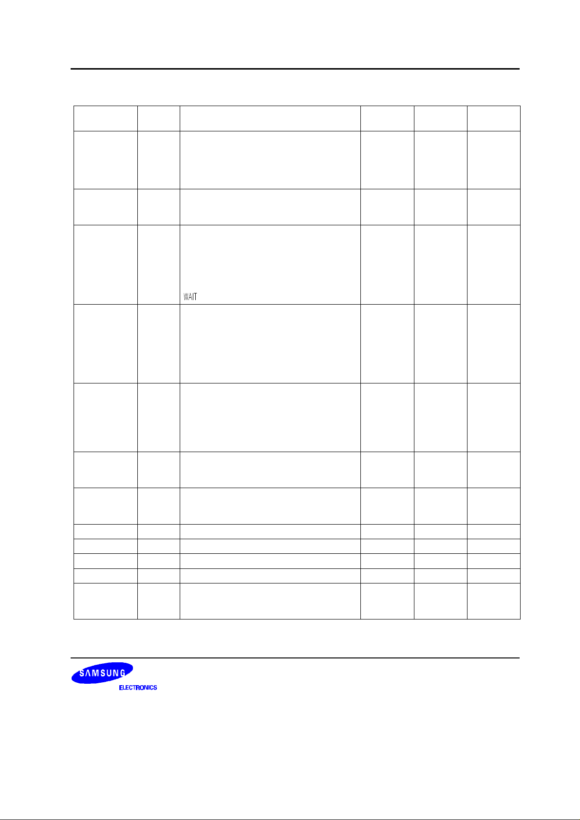
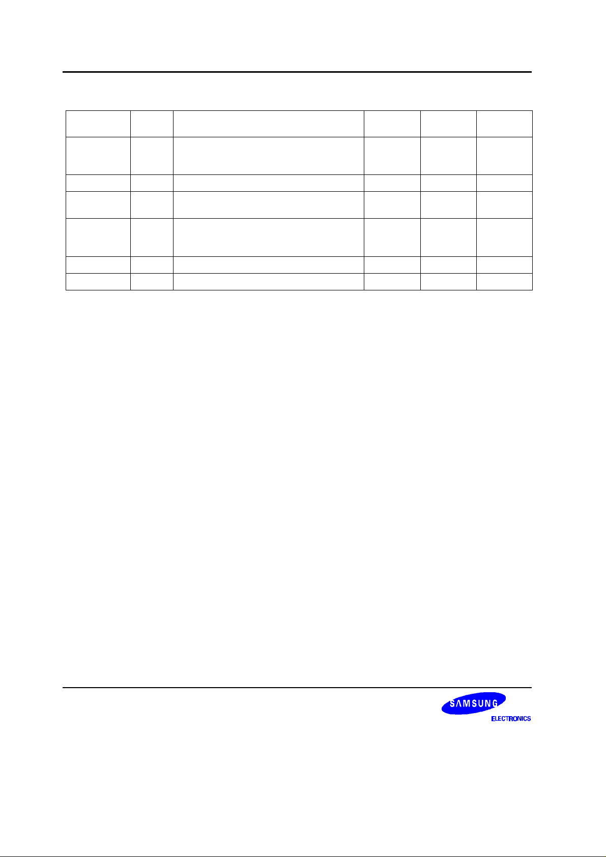
KS88C0716/P0716 PRODUCT OVERVIEW
PIN CIRCUIT
V
DD
Pull-Up Resistor
Pull-Up
Enable
Data
(Typical Value: 47 )
V
DD
K
Ω
Open-Drain
Output Disable
Pull-Up
Enable
Open-Drain
Data
In
Figure 1-4. Pin Circuit Type E (Ports 0, 1, 5)
V
DD
In/Out
V
DD
Pull-Up Resistor
(Typical Value: 47 )K
Ω
V
SS
Figure 1-5. Pin Circuit Type E-8 (Ports 6)
In/Out
1-9
 Loading...