

Samsung KS88C01116, KS88C01104, KS88C01016, KS88C01008, KS88C01004 Datasheet
...
KS88C01016/C01008/C01004/C01116/C01108/C01104 PRODUCT OVERVIEW
1 PRODUCT OVERVIEW
OVERVIEW
Samsung's KS88 series of 8-bit single-chip CMOS microcontrollers offers a fast and efficient CPU, a wide range
of integrated peripherals, and various mask-programmable ROM sizes. Important CPU features include:
— Efficient register-oriented architecture
— Selectable CPU clock sources
— Idle and Stop power-down mode release by interrupt
— Built-in basic timer with watchdog function
A sophisticated interrupt structure recognizes up to eight interrupt levels. Each level can have one or more
interrupt sources and vectors. Fast interrupt processing (within a minimum six CPU clocks) can be assigned to
specific interrupt levels.
KS88C01016/C01008/C01004/C01116/C01108/C01104 MICROCONTROLLER
The KS88C01016/C01008/C01004/C01116/C01108/C01104 single-chip CMOS microcontroller is fabricated
using a highly advanced CMOS process and is based on Samsung's newest CPU architecture.
The KS88C01016/C01008/C01004/C01116/C01108/C01104 is the microcontroller which has maskprogrammable ROM.
The KS88P01016/P01008/P01004/P01116/P01108/P01104 is the microcontroller which has one-timeprogrammable EPROM.
Using a proven modular design approach, Samsung engineers developed the
KS88C01016/C01008/C01004/C01116/C01108/C01104 by integrating the following peripheral modules with the
powerful SAM87 RC core:
— Three programmable I/O ports, including two 8-bit ports and one 3-bit port, for a total of 19 pins.
— Internal LVD circuit and eight bit-programmable pins for external interrupts.
— One 8-bit basic timer for oscillation stabilization and watchdog functions (system reset).
— One 8-bit timer/counter and one 16-bit timer/counter with selectable operating modes.
— One 8-bit counter with auto-reload function and one-shot or repeat control.
The KS88C01016/C01008/C01004/C01116/C01108/C01104 is a versatile general-purpose microcontroller
which is especially suitable for use as remote transmitter controller. It is currently available in a 24-pin SOP and
SDIP package
1-1

PRODUCT OVERVIEW KS88C01016/C01008/C01004/C01116/C01108/C01104
FEATURES
CPU
• SAM87RC CPU core
Memory
• Program memory (ROM)
- KS88C01016/C01116: 15,872-byte
(0000H-3E00H)
- KS88C01008/C01108: 8-Kbyte
(0000H-1FFFH)
- KS88C01004/C01104: 4-Kbyte
(0000H-0FFFH)
• Data memory: 256-byte RAM
Instruction Set
• 78 instructions
• IDLE and STOP instructions added for power-
down modes
Instruction Execution Time
• 500 ns at 8-MHz f
Interrupts
• 13 interrupt sources with 10 vector.
• 5 level, 10 vector interrupt structure
I/O Ports
• Two 8-bit I/O ports (P0-P1) and one 3-bit port
(P2) for a total of 19 bit-programmable pins
• Eight input pins for external interrupts
Carrier Frequency Generator
• One 8-bit counter with auto-reload function and
one-shot or repeat control (Counter A)
(minimum)
OSC
Timers and Timer/Counters
• One programmable 8-bit basic timer (BT) for
oscillation stabilization control or watchdog timer
function
• One 8-bit timer/counter (Timer 0) with two
operating modes; Interval mode and PWM mode.
• One 16-bit timer/counter with one operating
modes; Interval mode
Low Voltage Detect Circuit
• Low voltage detect for reset or Back-up mode.
• Low level detect voltage
– KS88C01016/C01008/C01004 :
2.20V (Typ) ±± 200 mV
– KS88C01116/C01108/C01104:
1.90V (Typ) ±± 200 mV
Auto Reset Function
• Reset occurs when stop mode is released by P0.
• When a falling edge is detected at Port 0 during
Stop mode, system reset occurs.
Operating Temperature Range
• –40°C to + 85°C
Operating Voltage Range
• 1.7 V to 3.6 V at 4 MHz f
• 2.0 V to 3.6 V at 8 MHz f
OSC
OSC
Package Type
• 24-pin SOP/SDIP
Back-up mode
• When V
is lower than V
DD
, the chip enters
LVD
Back-up mode to block oscillation and reduce the
current consumption.
1-2

KS88C01016/C01008/C01004/C01116/C01108/C01104 PRODUCT OVERVIEW
BLOCK DIAGRAM
P0.0-P0.7/INT0-INT4 P1.0-P1.7
LVD
TEST
X
IN
X
OUT
Main
OSC
8-bit
Basic
Port 0(INTR) Port 1
Internal Bus
Port I/O and Interrupt
Control
Port 2
P2.0/T0PWM
P2.1/REM
P2.2
Timer
8-bit
SAM87RI CPU
Timer/
Counter
Carrier
Generator
(Counter A)
256-Byte
Register File
16-bit
15-Kbyte ROM
Timer/
Counter
Figure 1-1. Block Diagram
1-3
PRODUCT OVERVIEW KS88C01016/C01008/C01004/C01116/C01108/C01104
PIN ASSIGNMENTS
V
DD
P2.2
P2.1/REM/
P2.0/T0PWN/T0CK/
SCLK
SDAT
P1.7
P1.6
P1.5
P1.4
P1.3
P1.2
P1.1
P1.0
P0.0/INT0/INTR
P0.1/INT1/INTR
RESET
/P0.2/INT2/INTR
P0.3/INT3/INTR
P0.4/INT4/INTR
P0.5/INT4/INTR
P0.6/INT4/INTR
P0.7/INT4/INTR
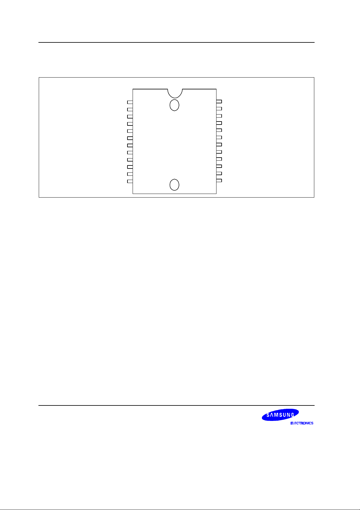
Figure 1-2. Pin Assignment Diagram (24-Pin SOP/SDIP Package)
V
SS
X
IN
X
OUT
TEST
1
2
3
4
KS88C01016/C01008
5
/C01004/C01116
6
/C01108/C01104
7
8
9
10
24-SOP/SDIP
(TOP VIEW)
11
12
24
23
22
21
20
19
18
17
16
15
14
13
1-4
KS88C01016/C01008/C01004/C01116/C01108/C01104 PRODUCT OVERVIEW
PIN DESCRIPTIONS
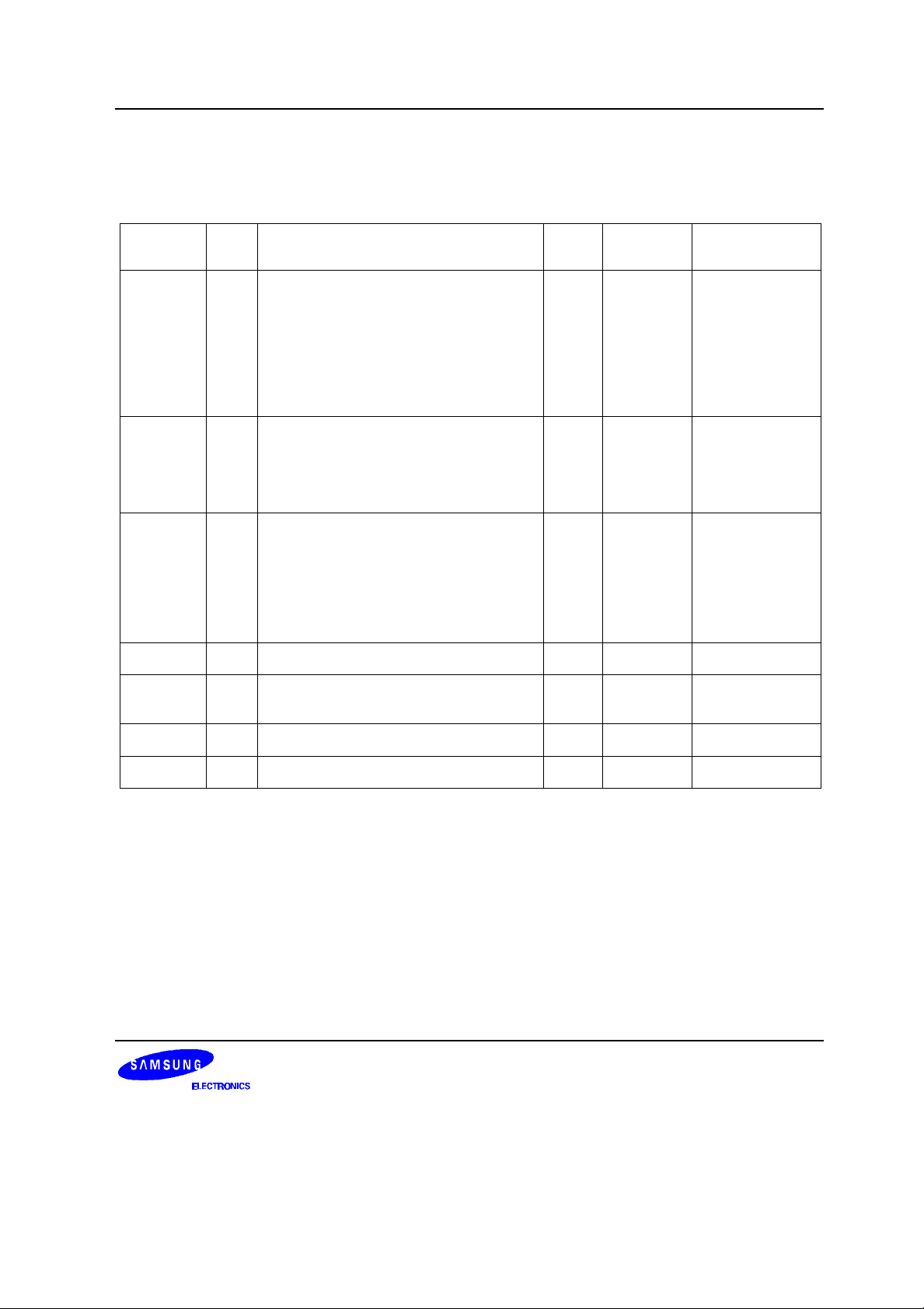
Table 1-1. Pin Descriptions
Pin
Names
Pin
Type
Pin
Description
P0.0-P0.7 I/O I/O port with bit-programmable pins.
Configurable to input or push-pull output
mode. Pull-up resistors are assignable by
software. Pins can be assigned individually
as external interrupt inputs with noise
filters, interrupt enable/ disable, and
interrupt pending control. Interrupt with
Reset(INTR) is assigned to Port 0.
P1.0-P1.7 I/O I/O port with bit-programmable pins.
Configurable to input mode or output
mode. Pin circuits are either push-pull or nchannel open-drain type. Pull-up resistors
are assignable by software.
P2.0
P2.1
P2.2
I/O 3-bit I/O port with bit-programmable pins.
Configurable to input mode, push-pull
output mode, or n-channel open-drain
output mode. Input mode with pull-up
resistors are assignable by software. The
two pins of port2 have high current drive
capability.
XIN, X
OUT
– System clock input and output pins – 2,3 –
Circuit
Type
24- Pin
Number
Shared
Functions
1 5-12 INT0 – INT4/INTR
2 13-20
3
21-23 REM/T0CK
4
5
TEST I Test signal input pin (for factory use only;
must be connected to VSS).
V
DD
V
SS
– Power supply input pin – 24 –
– Ground pin – 1 –
– 4 –
1-5
PRODUCT OVERVIEW KS88C01016/C01008/C01004/C01116/C01108/C01104
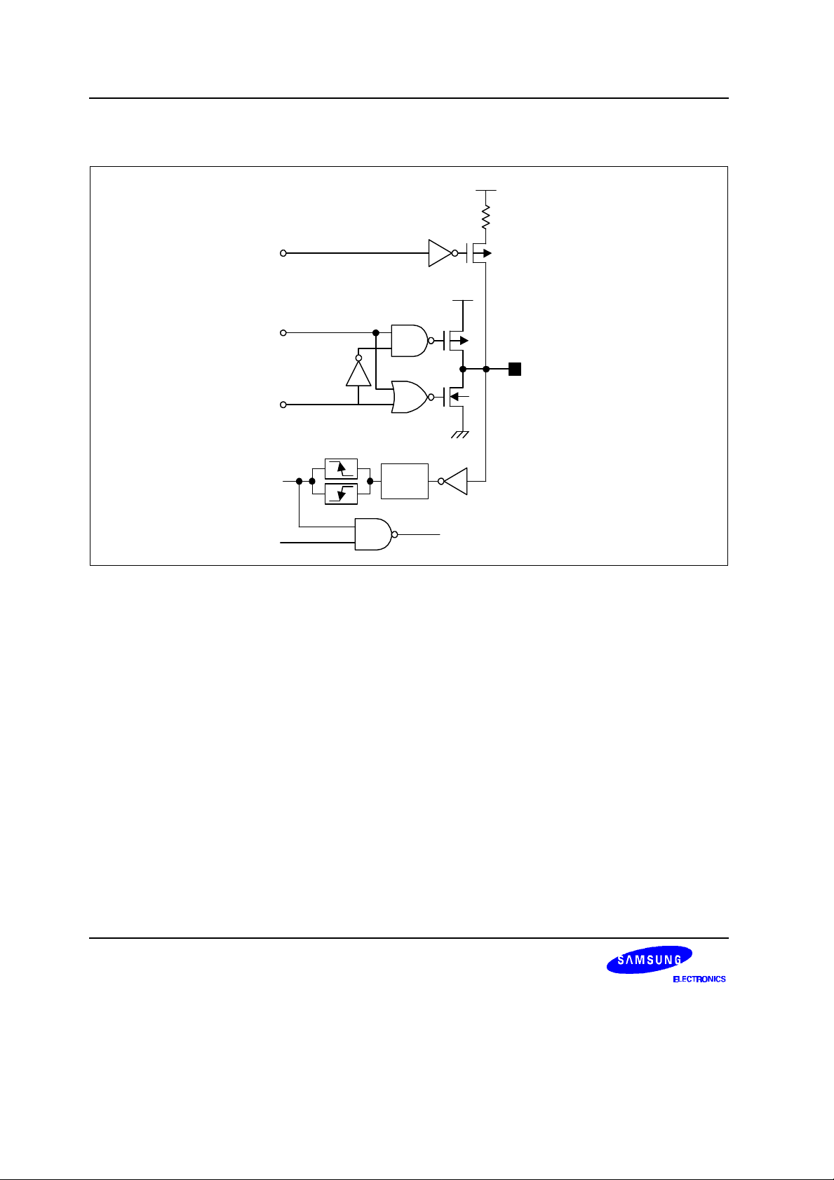
PIN CIRCUITS
V
DD
Pull-up
Resistor
Pull-up
Enable
V
DD
Data
Input/Output
Output
Disable
V
SS
External
Interrupt
Stop
Noise
filter
INTR (Interrupt with
RESET)
Figure 1-3. Pin Circuit Type 1 (Port 0)
NOTE
Interrupt with reset (INTR) is assigned to port 0 of KS88C01016/C01008/C01004/C01116/C01108
/C01104. It is designed to release stop status with reset. When the falling/rising edge is detected at any
pin of Port 0 during stop status, non vectored interrupt INTR signal occurs, after then system reset
occurs automatically. It is designed for a application which are using “stop mode” like remote controller.
If stop mode is not used, INTR do not operates and it can be discarded.
1-6
 Loading...