

Samsung KS8803BD, KS8803B Datasheet
KS8803B 10/15 CH PLL
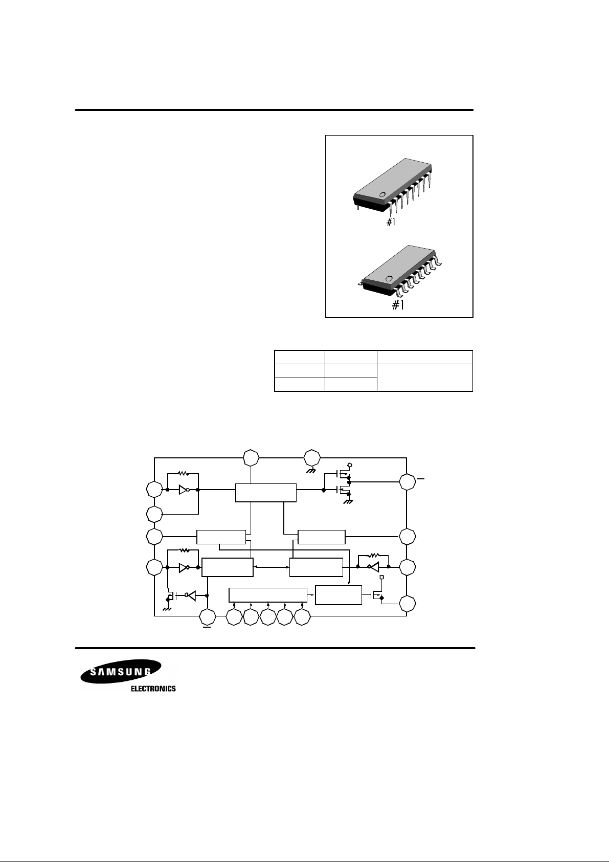
ORDERING INFORMATION
INTRODUCTION
The KS8803B/4B are designed to select 10/15 channels
of cordlss phone of which frequency band is 46/49MHz.
It has reference frequency generator, programmable divider for transmit and receive section and phase detector.
FEATURES
• 10 Channels selectable : KS8803B
(both transmit/receive)
• 15 Channels selectable : KS8804B
(both transmit/receive)
• Include oscillation circuit with external x-tal
(10.24MHz)
• 5KHz output for guard tone
• Unlock detector
(phase difference more than 6.25us)
• Stand-by function for power saving
BLOCK DIAGRAM
16-DIP-300A
16-SOP-225
Device Package Operating Temperature
KS8803B 16-DIP-300A
- 30°C ~ + 75°C
KS8803BD 16-SOP-225
OSC IN
OSC OUT
PDT
TIF
16
11
V
DD
15
REFERENCE
DIVIDER
V
12
SS
V
DD
+
F1
4
1
PHASE
DETECTOR (Tx)
9
PROGRAMMABLE
DIVIDER (Tx)
DECODER
5 6 7 8
SB D0 D1 D2 D3 MODE
PHASE
DETECTOR (Rx)
PROGRAMMABLE
DIVIDER (Rx)
UNLOCK
DETECTOR
23
13
PDR
14
10
RIF
LDT
+
KS8803B 10/15 CH PLL
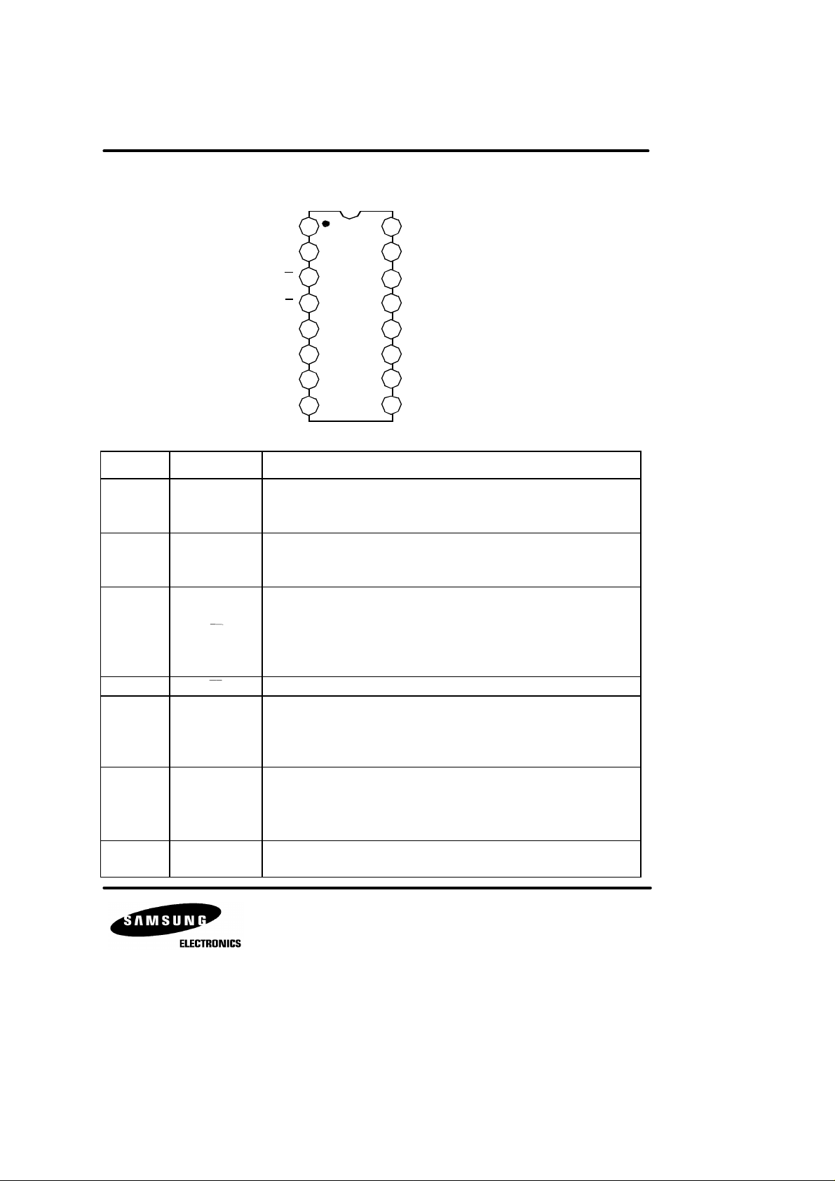
PIN CONFIGURATION
OSC OUT
MODE
1
2
3
SB
4
F1
16
OSC IN
V
15
DD
RIF
14
13
PDR
KS8803B
12
D0
5
D1
6
D2
7
8 9
D3
SS
V
PDT
11
10
LDT
TIF
PIN DESCRIPTION
Pin No Symbol Description
•This output generates reference frequency
1 OSC OUT
2 MODE
3 SB
4 F1
5
6
7
8
D0
D1
D2
D3
9 TIF
10 LDT
when it is connected to Pin 16 with external
OSC of which frequency is 10.24MHz
• Base/Remote Unit Selection Pin
“High” : Base Unit
“Low” : Remote Unit
• Stand-by pin
• This input controls Tx PLL for reducing
the power dissipation
“High” : Normal operation
“Low” : Stand-by
• 5KHz output
• Channel selection pins
• The Combinations of these inputs select
one channel among the 10/15 channels
• Input to programmable divider of Tx
• AC coupling with VCO
• In case of lager signal, It needs DC-coupling
• Min. input voltage is 0.1Vrms
• Unlocked signal out pin
(see output charateristics)

KS8803B 10/15 CH PLL
PIN DESCRIPTION
Pin No Symbol Description
• Phase detector output for Tx
11 PDT
12 V
SS
13 PDR
14 RIF
15 V
DD
16 OSC IN
• PDT detects the phase error from Tx PLL
and its output is connected to external low
pass filter
• This pin is negative supply of the IC.
• It usually grounded
• Phase detector output for Rx
• PDR detects the phase error from Rx PLL
and its output is connected to external low
pass filter
• Input of programmable divider for Rx.
• AC coupling with VCO
• In case of lager signal (standard CMOS
logic), it needs DC coupling
• Min. input voltage is 0.1Vrms
• This pin is positive supply of the IC
• Its reference is VSS, and normally
+ 3.0V ~ + 5.5V more positive than V
SS
• X-TAL osc connection pin
• This input generates the reference frequency
when it is connected to pin 1 with external
osc
 Loading...