

Samsung KS86C4104, KS86P4104, KS86P4004, KS86C4004 Datasheet

KS86C4004/P4004/C4104/P4104 PRODUCT OVERVIEW
1 PRODUCT OVERVIEW
SAM87RI PRODUCT FAMILY
Samsung's SAM87Ri family of 8-bit single-chip CMOS microcontrollers offers a fast and efficient CPU, a wide
range of integrated peripherals, and various mask-programmable ROM sizes.
A address/data bus architecture and a large number of bit-configurable I/O ports provide a flexible programming
environment for applications with varied memory and I/O requirements. Timer/counters with selectable operating
modes are included to support real-time operations.
KS86C4004/C4104 MICROCONTROLLER
The KS86C4004/C4104 single-chip 8-bit microcontroller is fabricated using an advanced CMOS process. It is
built around the powerful SAM87Ri CPU core. The KS86C4004/C4104 is a versatile microcontroller, with its A/D
converter and a zero-crossing detection capability it can be used in a wide range of general purpose applications.
Stop and Idle power-down modes were implemented to reduce power consumption. To increase on-chip register
space, the size of the internal register file was logically expanded. The KS86C4004/C4104 has 4-Kbytes of
program memory on-chip (ROM) and 208-bytes of general purpose register area RAM.
Using the SAM87Ri design approach, the following peripherals were integrated with the SAM87Ri core:
— Four configurable I/O ports (KS86C4004: 22 pins, KS86C4104: 16 pins)
— Six interrupt sources with one vector and one interrupt level
— Two 8-bit timer/counter with various operating modes
— Analog to digital converter (KS86C4004: 8-bit, 8-channel, KS86C4104: 10-bit, 5-channel)
— One zero cross detection module
The KS86C4004/C4104 microcontroller is ideal for use in a wide range of electronic applications requiring simple
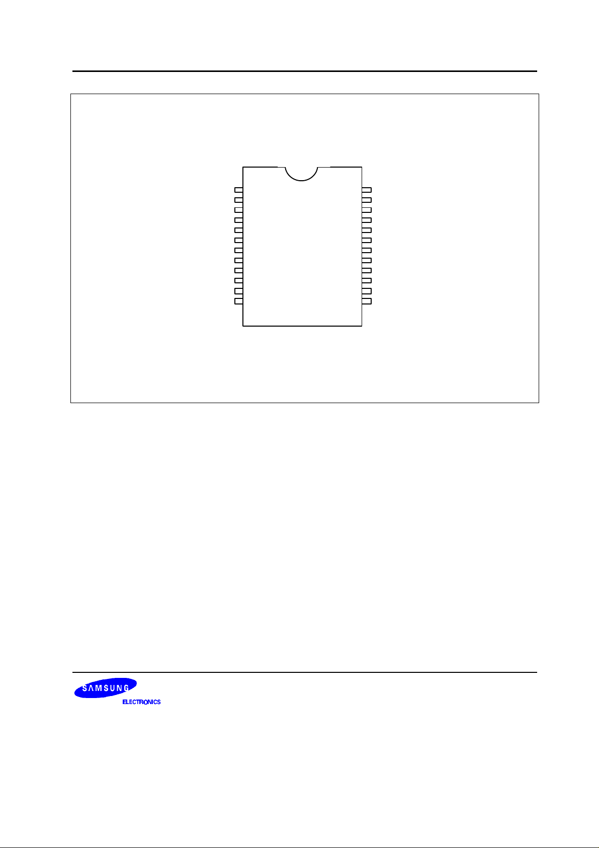
timer/counter, PWM, ADC, ZCD and capture functions. KS86C4004 is available in a 30-pin SDIP and a 32-pin
SOP package. KS86C4104 is available in a 24-pin SDIP and a 24-pin SOP package.
OTP
The KS86P4004/P4104 is an OTP (one time programmable) version of the KS86C4004/C4104 microcontroller.
The KS86P4004/P4104 has on-chip 4-Kbyte one-time programmable EEPROM instead of masked ROM. The
KS86P4004/P4104 is fully compatible with the KS86C4004/C4104, in function, in D.C. electrical characteristics
and in pin configuration.
1-1

PRODUCT OVERVIEW KS86C4004/P4004/C4104/P4104
FEATURES
CPU
• SAM87Ri CPU core
Memory
• 4-Kbyte internal program memory (ROM)
• 208-byte general purpose register area (RAM)
Instruction Set
• 41 instructions
• IDLE and STOP instructions added for
power-down modes.
Instruction Execution Time
• 600 ns at 10 MHz f
OSC
(minimum)
Interrupts
• 6 interrupt sources with one vector and one level
interrupt structure
Oscillation Frequency
• 1 MHz to 10 MHz external crystal oscillator
• Maximum 10 MHz CPU clock
• 4 MHz RC oscillator
General I/O
• Four I/O ports (22 pins for KS86C4004,
16 pins for KS86C4104)
• Bit programmable ports
Timer/Counter
• One 8-bit basic timer for watchdog function
• One 8-bit timer/counter with three operating
modes (10-bit PWM 1ch)
• One 8-bit timer/counter for the zero-crossing
detection circuit
Zero-Crossing Detection Circuit
• Zero-crossing detection circuit that generates a
digital signal in synchronism with an AC signal
input
Buzzer Frequency Range
• 200 Hz to 20 kHz signal can be generated
Operating Temperature Range
• – 40°C to + 85°C
Operating Voltage Range
• 2.7 V to 5.5 V
OTP Interface Protocol Spec
• Serial OTP
Package Types
• 30-pin SDIP, 32-pin SOP for KS86C4004/P4004
• 24-pin SDIP, 24-pin SOP for KS86C4104/P4104
A/D Converter
• Eight analog input pins
• 8-bit conversion resolution (KS86C4004)
• 10-bit conversion resolution (KS86C4104)
1-2
KS86C4004/P4004/C4104/P4104 PRODUCT OVERVIEW
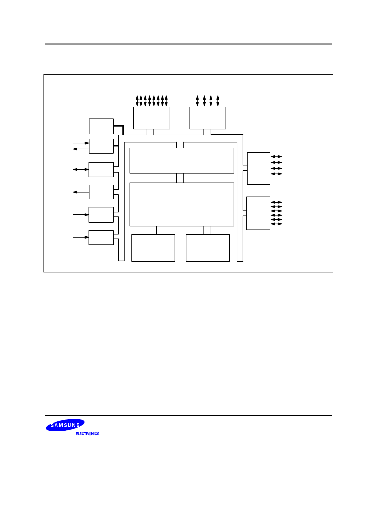
BLOCK DIAGRAM
P1.0-P1.3
P0.0-P0.7
/ZCD,BUZ,T0,CLO
X
X
OUT
T0(PWM)
P1.1/BUZ
ADC0
-ADC7
P1.0/
ZCD
BASIC
PORT 0
PORT 1
TIMER
IN
OSC
TIMER 0
I/O PORT I/O and
INTERRUPT CONTROL
PORT 2
P2.0-P2.3
/INT0-INT1
/ADC6-ADC7
TIMER 1
SAM87RI CPU
ADC
ZCD
4-KB ROM
REGISTER FILE
Figure 1-1. Block Diagram
PORT 3
208-BYTE
P3.0-P3.5
/ADC0-ADC5
1-3
PRODUCT OVERVIEW KS86C4004/P4004/C4104/P4104
PIN ASSIGNMENTS
V
SS
X
X
OUT
TEST
P0.1
P0.0
RESET
P3.5/ADC5
P3.4/ADC4
P3.3/ADC3
P3.2/ADC2
P3.1/ADC1
P3.0/ADC0
AV
SS
AV
ref
IN
1
2
3
4
5
6
7
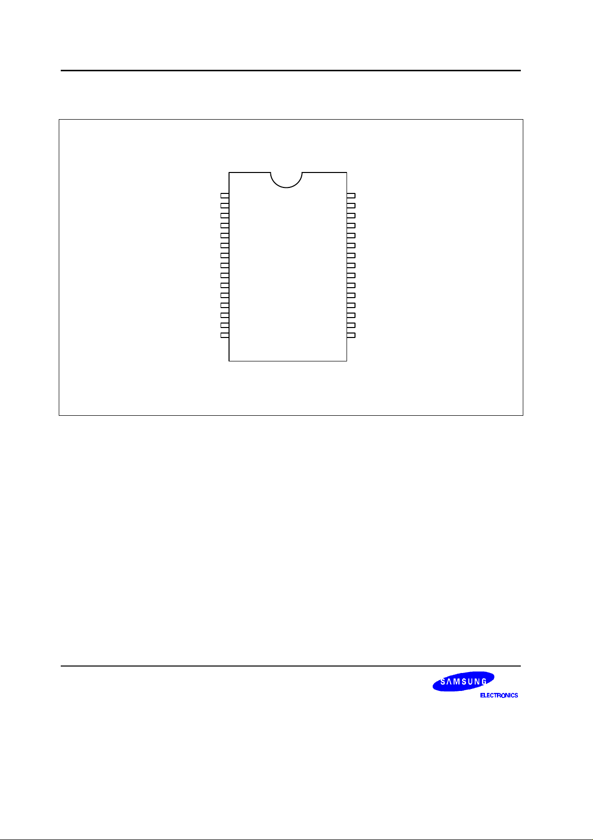
KS86C4004
8
9
10
11
12
13
14
15
30-SDIP
(Top View)
30
29
28
27
26
25
24
23
22
21
20
19
18
17
16
VDD
P0.2
P0.3
P0.4
P0.5
P0.6
P0.7
P1.0 / ZCD
P1.1 / BUZ
P1.2 / T0(PWM)
P1.3 / CLO
P2.0 / INT0
P2.1 / INT1
P2.2 / ADC6
P2.3 / ADC7
Figure 1-2. Pin Assignment Diagram (30-Pin SDIP Package)
1-4
KS86C4004/P4004/C4104/P4104 PRODUCT OVERVIEW
V
SS
X
X
OUT
TEST
P0.1
P0.0
RESET
NC
P3.5/ADC5
P3.4/ADC4
P3.3/ADC3
P3.2/ADC2
P3.1/ADC1
P3.0/ADC0
AV
SS
AV
ref
IN
1
2
3
4
5
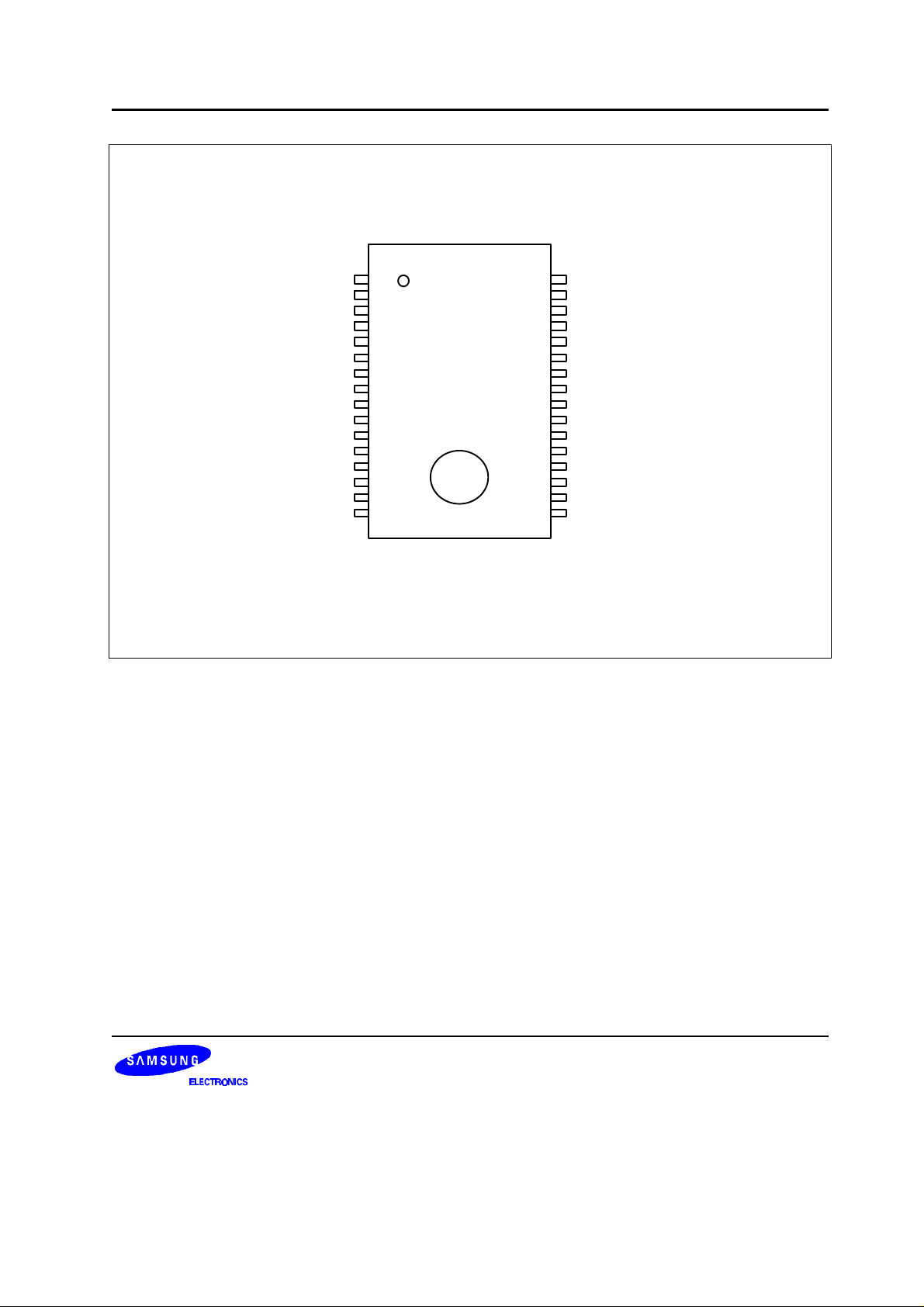
KS86C4004
6
7
8
(Top View)
9
10
11
12
13
14
15
16
32-SOP
32
31
30
29
28
27
26
25
24
23
22
21
20
19
18
17
V
DD
P0.2
P0.3
P0.4
P0.5
P0.6
P0.7
NC
P1.0 / ZCD
P1.1 / BUZ
P1.2 / T0(PWM)
P1.3 / CLO
P2.0 / INT0
P2.1 / INT1
P2.2 / ADC6
P2.3 / ADC7
Figure 1-3. Pin Assignment Diagram (32-Pin SOP Package)
1-5
PRODUCT OVERVIEW KS86C4004/P4004/C4104/P4104
V
SS
X
X
OUT
TEST
P0.1
P0.0
RESET
P3.4/ADC4
P3.3/ADC3
P3.2/ADC2
P3.1/ADC1
P3.0/ADC0
IN
1
2
3
4
5
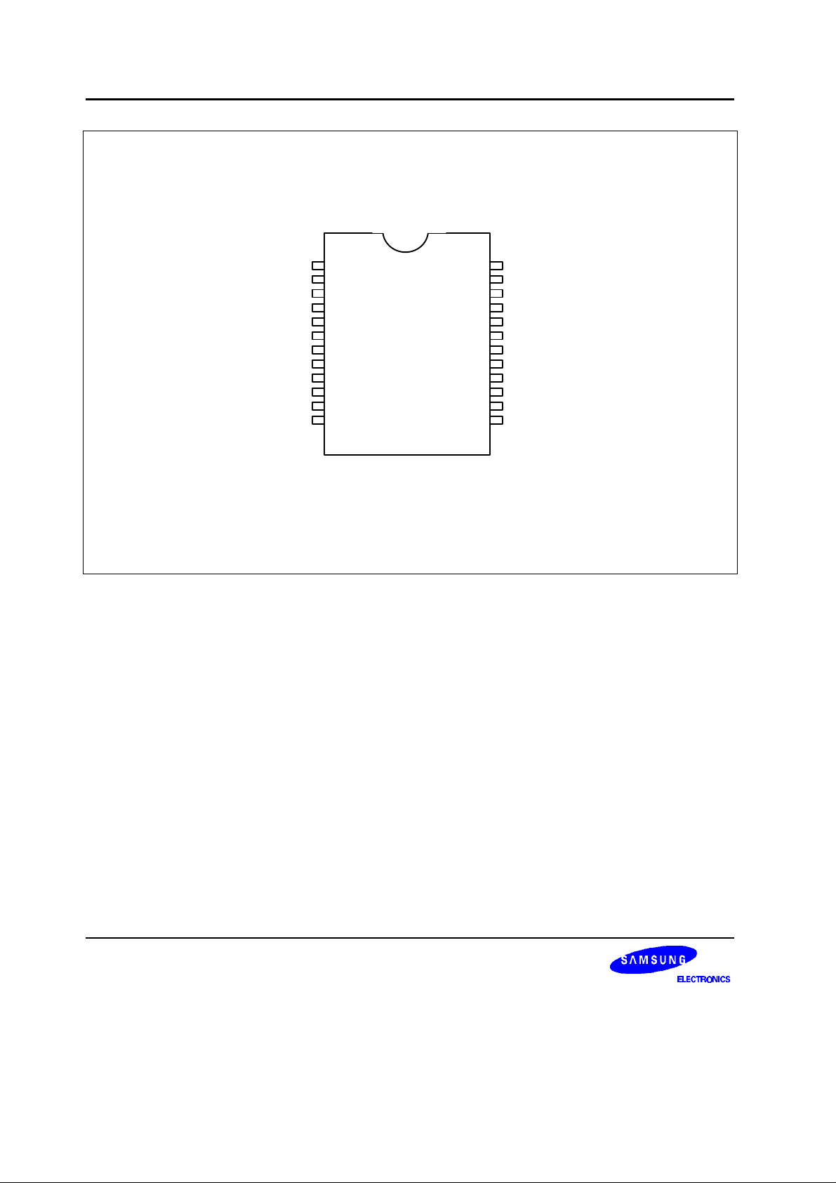
KS86C4104
6
7
8
9
10
11
12
24-SDIP
(Top View)
24
23
22
21
20
19
18
17
16
15
14
13
VDD
P0.2
P0.3
P0.4
P0.5
P0.6
P1.0 / ZCD
P1.1 / BUZ
P1.2 / T0(PWM)
P2.0 / INT0
AV
ref
AV
SS
Figure 1-4. Pin Assignment Diagram (24-Pin SDIP Package)
1-6
KS86C4004/P4004/C4104/P4104 PRODUCT OVERVIEW
V
SS
X
X
OUT
TEST
P0.1
P0.0
RESET
P3.4/ADC4
P3.3/ADC3
P3.2/ADC2
P3.1/ADC1
P3.0/ADC0
IN
1
2
3
4
5
KS86C4104
6
7
(Top View)
8
9
10
11
12
24-SOP
24
23
22
21
20
19
18
17
16
15
14
13
VDD
P0.2
P0.3
P0.4
P0.5
P0.6
P1.0 / ZCD
P1.1 / BUZ
P1.2 / T0(PWM)
P2.0 / INT0
AV
ref
AV
SS
Figure 1-5. Pin Assignment Diagram (24-Pin SOP Package)
1-7
PRODUCT OVERVIEW KS86C4004/P4004/C4104/P4104
PIN DESCRIPTIONS
Table 1-1. KS86C4004/C4104 Pin Descriptions
Pin
Names
P0.0-P0.7 I/O
Pin
Type
Pin
Description
Bit-programmable I/O port for normal input or
Circuit
Type
E-2
Share
Pins
push-pull, open-drain output. Pull-up resistors are
assignable by software.
P1.0-P1.3 I/O Bit-programmable I/O port for Schmitt trigger
input or push-pull output. Pull-up resistors are
assignable by software. Port 1 pins can also be
used as alternative functions.
P2.0-P2.3 I/O Bit-programmable I/O port for Schmitt trigger
input or push-pull, open drain output. Pull up
F
D
D
D
E
E-1
ZCD
BUZ
T0(PWM)
CLO
INT0–INT1
ADC6–ADC7
resistors are assignable by software. Port 2 can
also be used as external interrupt, A/D input.
P3.0-P3.5 I/O Bit-programmable I/O port for Schmitt trigger
F ADC0–ADC5
input or push-pull output. Pull-up resistors are
assignable by software. Port 3 pins can also be
used as A/D converter input.
XIN, X
OUT
–
Crystal/ceramic, or RC oscillator signal for
– –
system clock.
INT0–INT1 I External interrupt input. E P2.0–P2.1
RESET
TEST I Test signal input pin (for factory use only: must be
I System RESET signal input pin. B –
– –
connected to VSS)
V
DD, VSS
AV
REF,
AV
SS
– Voltage input pin and ground – –
– A/D converter reference voltage input and ground – –
ZCD I Zero crossing detector input F P1.0
BUZ O 200 Hz–20 kHz frequency output for buzzer sound D P1.1
T0 I/O Timer 0 capture input or 10-bit PWM output D P1.2
CLO O System clock output port D P1.3
ADC0–ADC7 I A/D converter input F
E-1
P3.0–P3.5
P2.2–P2.3
NOTE: Port 0.7, P1.3, P2.1–P2.3 and P3.5 is not available in KS86C4104/P4104 .
1-8
KS86C4004/P4004/C4104/P4104 PRODUCT OVERVIEW
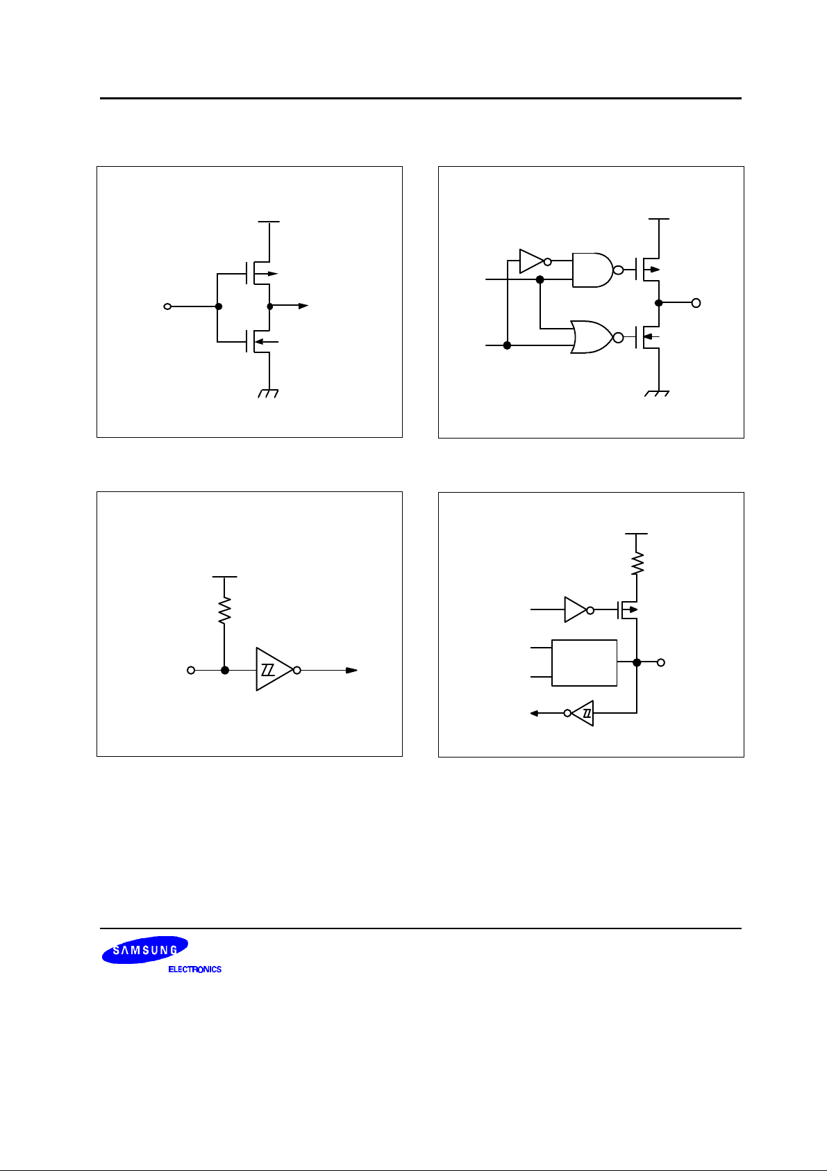
PIN CIRCUITS
V
DD
V
DD
P-CHANNEL
IN
N-CHANNEL
Figure 1-6. Pin Circuit Type A
V
DD
PULL-UP
RESISTOR
IN
DATA
OUTPUT
DISABLE
RESISTOR
ENABLE
OUTPUT
DISABLE
Figure 1-8. Pin Circuit Type C
V
DD
DATA
CIRCUIT
TYPE C
P-CHANNEL
OUT
N-CHANNEL
PULL-UP
RESISTOR
P-CHANNEL
IN/OUT
Figure 1-7. Pin Circuit Type B
DATA
Figure 1-9. Pin Circuit Type D
1-9
PRODUCT OVERVIEW KS86C4004/P4004/C4104/P4104
PNE
DATA
OUTPUT
DISABLE
INPUT
PNE
V
V
DD
DD
P-CH
N-CH
Figure 1-10. Pin Circuit Type E
V
DD
V
DD
PULL-UP
RESISTOR
PULL-UP
RESISTOR
PULL-UP
ENABLE
IN/OUT
PNE
DATA
OUTPUT
DISABLE
INPUT
V
V
DD
DD
PULL-UP
RESISTOR
P-CH
PULL-UP
ENABLE
N-CH
Figure 1-10. Pin Circuit Type E-2
V
DD
PULL-UP
RESISTOR
IN/OUT
DATA
OUTPUT
DISABLE
DIGITAL INPUT
ANALOG INPUT
Figure 1-11. Pin Circuit Type E-1
1-10
P-CH
N-CH
PULL-UP
ENABLE
IN/OUT
PULL-UP
ENABLE
DATA
OUTPUT
DISABLE
DIGITAL
INPUT
ANALOG
INPUT
V
DD
CIRCUIT
TYPE C
Figure 1-12. Pin Circuit Type F
IN/OUT

KS86C4004/P4004/C4104/P4104 ELECTRICAL DATA
13 ELECTRICAL DATA
OVERVIEW
In this section, the following KS86C4004/C4104 electrical characteristics are presented in tables and graphs:
— Absolute maximum ratings
— D.C. electrical characteristics
— A.C. electrical characteristics
— Oscillator characteristics
— Oscillation stabilization time
— Operating Voltage Range
— Schmitt trigger input characteristics
— Data retention supply voltage in Stop mode
— Stop mode release timing when initiated by a RESET
— A/D converter electrical characteristics
— Zero-crossing detector
— Zero Crossing Waveform Diagram
13-1
 Loading...