

Samsung KS86P6408, KS86C6408, KS86C6404 Datasheet

KS86C6404/C6408/P6408 PRODUCT OVERVIEW
1 PRODUCT OVERVIEW
SAM87RI PRODUCT FAMILY
Samsung's SAM87RI family of 8-bit single-chip CMOS microcontrollers offers a fast and efficient CPU, a wide
range of integrated peripherals, and various mask-programmable ROM sizes.
A dual address/data bus architecture and a large number of bit- or nibble-configurable I/O ports provide a flexible
programming environment for applications with varied memory and I/O requirements. Timer/counters with
selectable operating modes are included to support real-time operations. Many SAM87RI microcontrollers have
an external interface that provides access to external memory and other peripheral devices.
KS86C6404/C6408/P6408 MICROCONTROLLER
The KS86C6404/C6408/P6408 single-chip 8-bit microcontroller is fabricated using an advanced CMOS process.
It is built around the powerful SAM87RI CPU core.
Stop and Idle power-down modes were implemented to reduce power consumption. To increase on-chip register
space, the size of the internal register file was logically expanded. The KS86C6404 has 4 K bytes of program
memory on-chip and KS86C6408 has 8 K bytes.
Using the SAM87RI design approach, the following peripherals were integrated with the SAM87RI core:
— Five configurable I/O ports (32 pins)
— 20 bit-programmable pins for external interrupts
— 8-bit timer/counter with three operating modes
— Low speed USB function
The KS86C6404/C6408/P6408 is a versatile microcontroller that can be used in a wide range of low speed USB
support general purpose applications. It is especially suitable for use as a keyboard controller and is available in
a 42-pin SDIP and a 44-pin QFP package.
OTP
The KS86C6404/C6408 microcontroller is also available in OTP (One Time Programmable) version,
KS86P6408. KS86P6408 microcontroller has an on-chip 8-Kbyte one-time-programmable EPROM instead of
masked ROM. The KS86P6408 is comparable to KS86C6404/C6408, both in function and in pin configuration.
1-1

PRODUCT OVERVIEW KS86C6404/C6408/P6408
FEATURES
CPU
• SAM87RI CPU core
Memory
• 4/8-Kbyte internal program memory (ROM)
• 208-byte RAM
Instruction Set
• 41 instructions
• IDLE and STOP instructions added for powerdown modes
Instruction Execution Time
• 1.0 µs at 6 MHz f
OSC
Interrupts
• 25 interrupt sources with one vector, each
source has its pending bit
• One level, one vector interrupt structure
Oscillation Circuit
Timer/Counter
• One 8-bit basic timer for watchdog function and
programmable oscillation stabilization interval
generation function
• One 8-bit timer/counter with Compare/Overflow
USB Serial Bus
• Compatible to USB low speed (1.5 Mbps) device
1.0 specification.
• 1 Control endpoint and 2 Data endpoint
• Serial bus interface engine (SIE)
— Packet decoding/generation
— CRC generation and checking
— NRZI encoding/decoding and bit-stuffing
• 8 bytes each receive/transmit USB buffer
Operating Temperature Range
• – 40 °C to + 85 °C
• 6 MHz crystal/ceramic oscillator
• External clock source (6 MHz)
General I/O
• Bit programmable five I/O ports (34 pins total)
— (D+/PS2, D-/PS2 Included)
Operating Voltage Range
• 4.0 V to 5.25 V
Package Types
• 42-pin SDIP
• 44-pin QFP
1-2
KS86C6404/C6408/P6408 PRODUCT OVERVIEW
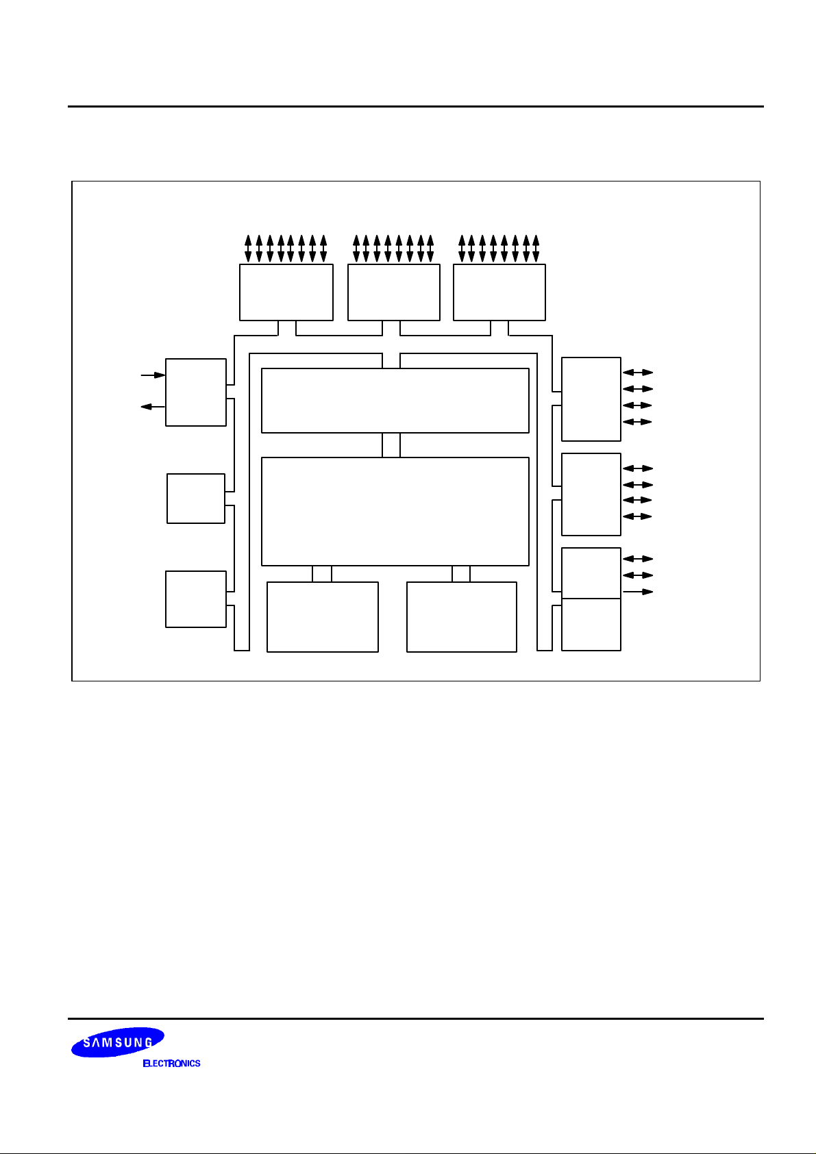
BLOCK DIAGRAM
X
X
OUT
P0.0-P0.7/INT2
Port 0
IN
OSC
Basic
Timer
TIMER 0
4/8-KB ROM
P1.0-P1.7
Port 1 Port 2
SAM87RI BUS
I/O Port And
Interrupt Control
SAM87RI CPU
208-Byte
Register
P2.0-P2.7 / INT0
Port 3
Port 4
USB
16 bytes
USB
Buffer
P3.0
P3.1
P3.2
P3.3/CLO
P4.0 / INT1
P4.1 / INT1
P4.2 / INT1
P4.3 / INT1
D+/PS2
D-/PS2
3.3 V
OUT
Figure 1-1. Block Diagram
1-3
PRODUCT OVERVIEW KS86C6404/C6408/P6408
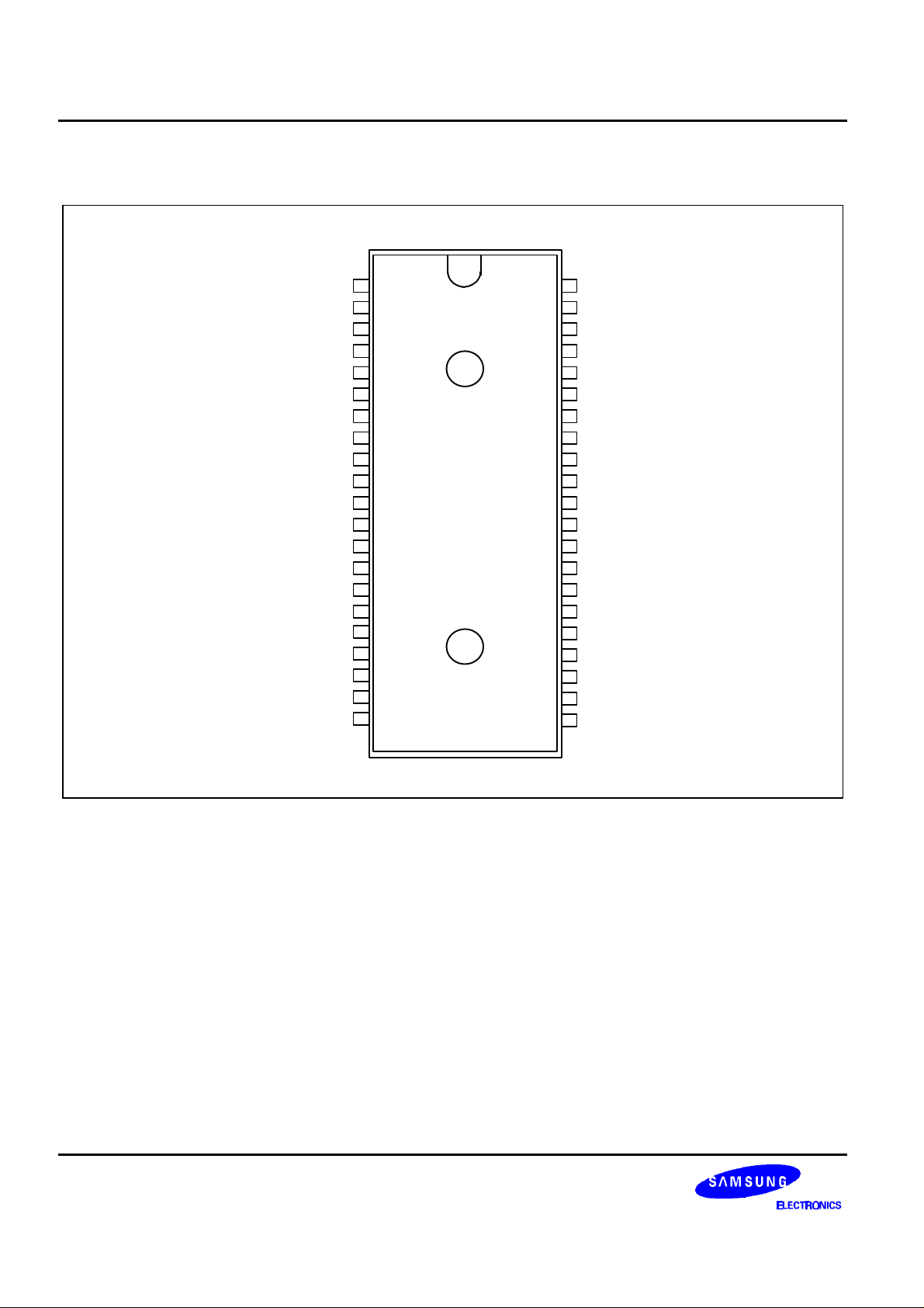
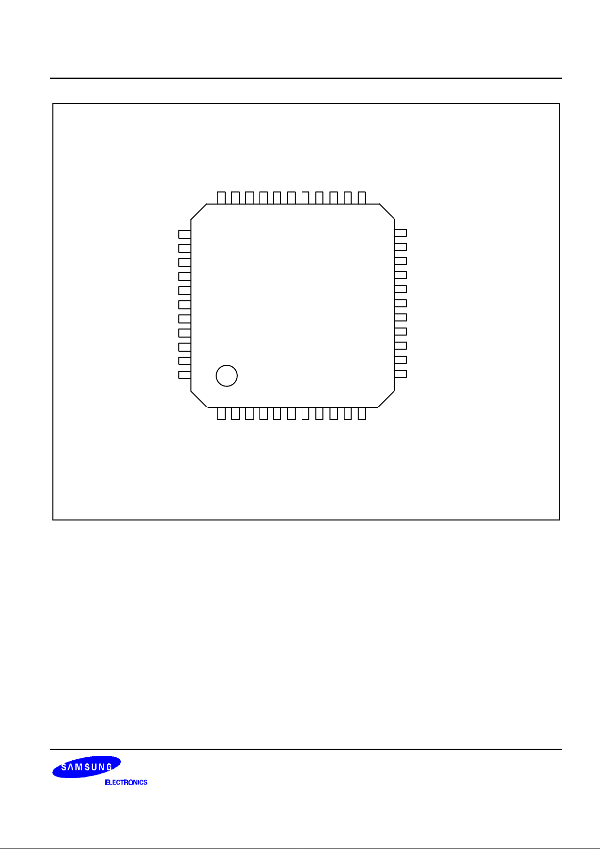
PIN ASSIGNMENTS
P3.1
P3.0
INT0 / P2.0
INT0 / P2.1
INT0 / P2.2
INT0 / P2.3
INT0 / P2.4
INT0 / P2.5
INT0 / P2.6
INT0 / P2.7
V
V
X
OUT
X
TEST
INT1 / P4.0
INT1 / P4.1
RESET
INT1 / P4.2
INT1 / P4.3
P1/7
DD
SS
1
2
3
4
5
6
7
8
9
KS86C6404
10
KS86C6408
11
12
42-SDIP
(Top View)
13
IN
14
15
16
17
18
19
20
21
42
41
40
39
38
37
36
35
34
33
32
31
30
29
28
27
26
25
24
23
22
P3.2
P3.3/CLO
D+/PS2
D-/PS2
3.3 V
OUT
NC
P0.0 / INT
P0.1 / INT
P0.2 / INT
P0.3 / INT
P0.4 / INT
P0.5 / INT
P0.6 / INT
P0.7 / INT
P1.0
P1.1
P1.2
P1.3
P1.4
P1.5
P1.6
1-4
Figure 1-2. Pin Assignment Diagram (42-Pin SDIP Package)
KS86C6404/C6408/P6408 PRODUCT OVERVIEW
INT0 / P2.4
INT0 / P2.5
INT0 / P2.6
INT0 / P2.7
NC
NC
NC
P0.0/INT2
P0.1/INT2
P0.2/INT2
P0.3/INT2
P0.4 /INT2
P0.5/INT2
P0.6/INT2
P0.7/INT2
33
32
31
30
29
28
27
26
25
24
23
3.3 V
OUT
D-/PS2
D+/PS2
P3.3/CLO
P3.2
P3.1
P3.0
P2.0/INT0
P2.1/INT0
P2.2/INT0
P2.3/INT0
34
35
36
37
38
39
40
41
42
43
44
1
KS86C6404
KS86C6408
(Top View)
2
3
4 5 6
7
8
9
10
SS
VDD
XIN
V
XOUT
TEST
22
21
20
19
18
17
16
15
14
13
12
11
P4.0/INT1
P4.1/INT1
P1.0
P1.1
P1.2
P1.3
P1.4
P1.5
P1.6
P1.7
P4.3/INT1
P4.2/INT1
RESET
Figure 1-3. Pin Assignment Diagram (44-Pin QFP Package)
1-5
PRODUCT OVERVIEW KS86C6404/C6408/P6408
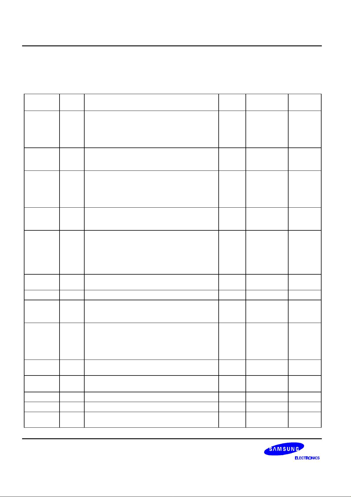
PIN DESCRIPTIONS
Table 1-1. KS86C6404/C6408/P6408 Pin Descriptions
Pin
Names
P0.0-P0.7 I/O Bit-programmable I/O port for Schmitt trigger
Pin
Type
Pin
Description
Circuit
Number
B 36-29
input or open-drain output. Port0 can be
individually configured as external interrupt
inputs. Pull-up resistors are assignable by
software.
P1.0-P1.7 I/O Bit-programmable I/O port for Schmitt trigger
B 28-21
input or open-drain output. Pull-up resistors are
assignable by software.
P2.0-P2.7 I/O Bit-programmable I/O port for Schmitt trigger
B 3-10
input or open-drain output. Port2 can be
individually configured as external interrupt
inputs. Pull-up resistors are assignable by
software.
P3.0-P3.3 I/O Bit-programmable I/O port for Schmitt trigger
C 2, 1, 42, 41
input, open-drain or push-pull output. P3.3 can
be used to system clock output(CLO) pin.
P4.0-P4.3 I/O Bit-programmable I/O port for Schmitt trigger
D 16, 17, 19, 20
input or open-drain output or push-pull output.
Port4 can be individually configured as external
interrupt inputs. In output mode, pull-up resistors
are assignable by software. But in input mode,
pull-up resistors are fixed.
D+/PS2
D-/PS2
3.3 V
XIN, X
OUT
OUT
I/O Programmable port for
– 40-39 (36-35) –
USB interface or PS2 interface.
– 3.3 V output from internal voltage regulator – 38 (34) –
– System clock input and output pin
– 14, 13
(crystal/ceramic oscillator, or external clock
source)
INT0
INT1
I External interrupt for bit-programmable port0,
port2 and port4 pins when set to input mode.
– 3-10, 16,17,
INT2
RESET I RESET signal input pin. Input with internal pull-
A 18 (12) –
up resistor.
TEST I Test signal input pin (for factory use only;
– 15 (9) –
connected to VSS)
V
DD
V
SS
– Power input pin – 11 (5) –
– Ground input pin – 12, (6) –
NC – No connection – 37
Pin
Numbers
(30-23)
(22-15)
(41-44, 1-4)
(40-37)
(10, 11, 13,
14)
(8, 7)
19, 20, 29-36
(30-23, 41-44,
1-4, 10, 11,
13, 14)
(31,32, 33)
Share
Pins
INT2
–
INT0
P3.3/CLO
INT1
–
PORT2/
PORT4/
PORT0
–
NOTE: Pin numbers shown in parenthesis '( )' are for the 44-QFP package; others are for the 42-SDIP package.
1-6
KS86C6404/C6408/P6408 PRODUCT OVERVIEW
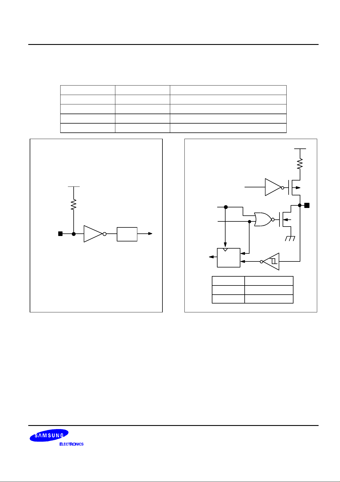
PIN CIRCUITS
Table 1-2. Pin Circuit Assignments for the KS86C6404/C6408/P6408
Circuit Number Circuit Type KS86C6404/C6408/P6408 Assignments
A I RESET signal input
B I/O Ports 0, 1, and 2
C I/O Port 3
D I/O Port 4
V
DD
Pull-Up
Resistor
V
DD
Pull-Up Enable
PULL-UP
RESISTOR
IN
Noise
Filter
Figure 1-4. Pin Circuit Type A (RESET)
Output
Disable
Output
Data
Input
Data
D0
MUX
D1
Mode Input Data
Output D0
Input
D1
V
SS
I/O
Figure 1-5. Pin Circuit Type B (Ports 0, 1 and 2)
1-7
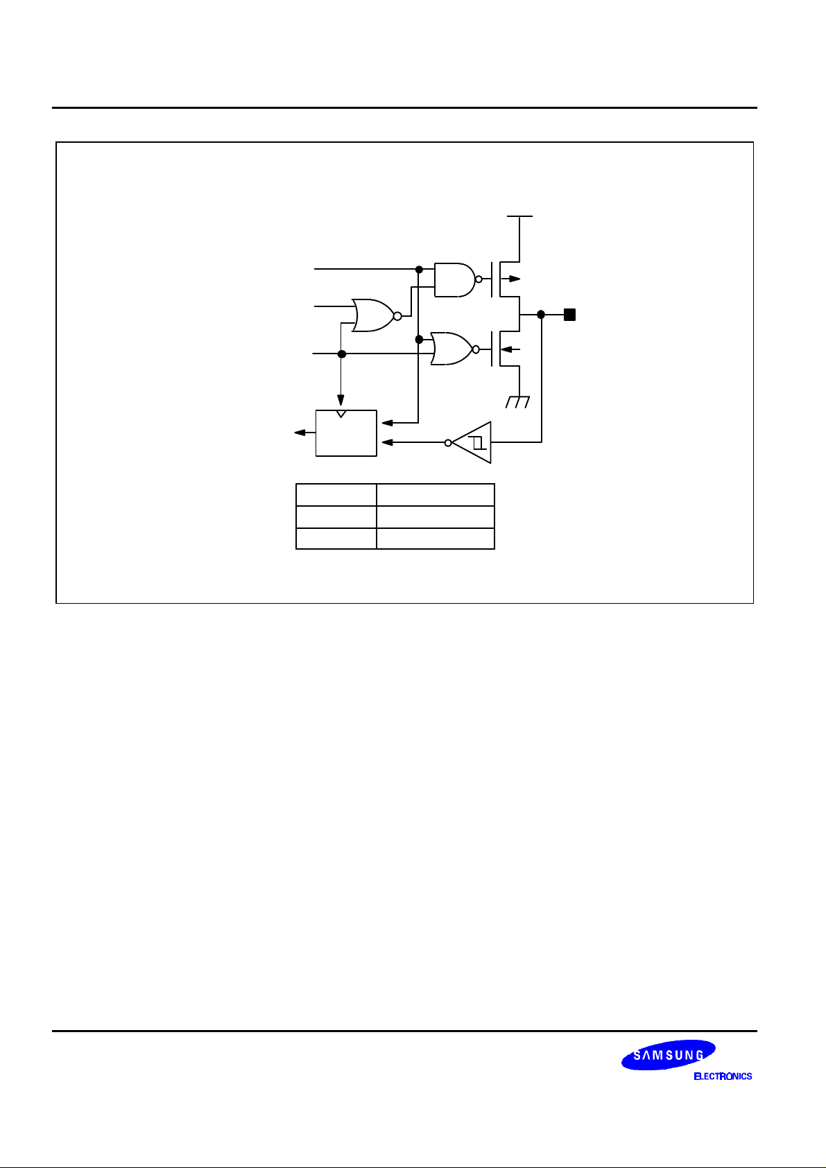
PRODUCT OVERVIEW KS86C6404/C6408/P6408
V
DD
Output
Data
Open
Drain
I/O
Output
Disable
V
SS
Input
Data
MUX
D0
D1
Mode Input Data
Output D0
Input
D1
Figure 1-6. Pin Circuit Type C (Port 3)
1-8
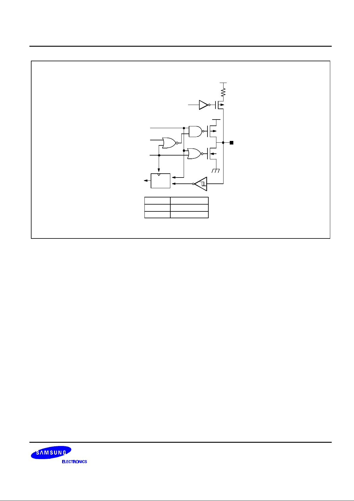
KS86C6404/C6408/P6408 PRODUCT OVERVIEW
DD
V
Pull-Up
Resistor
Pull-Up
Enable
DD
V
Output
Data
Open
Drain
Output
Disable
Input
Data
Output D0
D0
MUX
D1
Mode Input Data
Input
D1
V
SS
I/O
Figure 1-7. Pin Circuit Type D (Port 4)
1-9
 Loading...