

Samsung K4D263238M-QC45, K4D263238M-QC55, K4D263238M-QC50, K4D263238M-QC60 Datasheet

K4D263238M
128M DDR SDRAM
128Mbit DDR SDRAM
1M x 32Bit x 4 Banks
Double Data Rate Synchronous RAM
with Bi-directional Data Strobe and DLL
Revision 1.3
August 2001
Samsung Electronics reserves the right to change products or specification without notice.
- 1 -
Rev. 1.3 (Aug. 2001)

K4D263238M
128M DDR SDRAM
Revision History
Revision 1.3 (August 2, 2001)
• Removed K4D263238M-QC40 with VDD&VDDQ=2.8V
• Changed VDD&VDDQ of K4D263238M-QC45 from 2.8V to 2.5V.
• Changed tCK(max) from 7ns to 10ns.
Revision 1.2 (July 12, 2001)
• Corrected CAS latency of K4D263238M-QC45 from CL3 to CL4
• The specification for the 222MHz/250MHz is preliminary one.
Revision 1.1 (March 5, 2000)
• Added K4D263238M-QC40 with VDD&VDDQ=2.8V
• Changed VDD/VDDQ of K4D263238M-QC45 from 2.5V to 2.8V. Accordingly, DC current characteristics values have been changed.
- Changed CAS latency of K4D263238M-QC45 from CL4 to CL3.
• Changed tWPREH of K4D263238M-QC50 from 0.3tCK to 0.25tCK
- 2 -
Rev. 1.3 (Aug. 2001)
K4D263238M
128M DDR SDRAM
Revision 1.0 (December 13, 2000)
• Defined capacitance values
• Chagned tRCDWR of K4D263238M-QC60 from 1tCK to 2tCK
Revision 0.5 (December 8, 2000)
• Changed AC input level from Vref + 0.31V to Vref + 0.35V
• Changed tRC/tRFC/tRAS/tRP/tRCDRD/tRCDWR from ns unit based from clock unit based.
• Changed VIN /VOUT/VDDQ in absolute maximum ratings from -1.0V ~3.6V to -0.5V ~ 3.6V.
Revision 0.4 (November 29, 2000) - Preliminary
• Removed K4D263238M-QC40
• Several AC parameters of K4D263238M-QC45 have been changed
- Changed tDQSQ from 0.4ns to 0.45ns. Changed tQH from tHP-0.6ns to tHP-0.45ns.
- Changed tDQSCK & tAC from 0.6ns to 0.7ns
- Changed tDQSS from 0.75tCK/1.25tCK to 0.8tCK/1.2tCK. Accordingly, changed tWPREH from 0.25tCK to 0.3tCK.
- Changed tDS/tDH from 0.4ns to 0.45ns. Changed tIS/tIH from 0.9ns to 1.0ns
- Corrected tDAL from 5tCK to 6tCK
• Several AC parameters of K4D263238M-QC50 have been changed
- Changed tQH from tHP-0.6ns to tHP-0.45ns.
- Changed tDQSCK & tAC from 0.6ns to 0.7ns
- Changed tDQSS from 0.75tCK/1.25tCK to 0.8tCK/1.2tCK. Accordingly, changed tWPREH from 0.25tCK to 0.3tCK.
- Corrected tDAL from 5tCK to 6tCK
• Several AC parameters of K4D263238M-QC55 have been changed
- Changed tDQSQ from 0.45ns to 0.5ns. Changed tOH from tHP-0.6ns to tHP-0.5ns.
- Changed tDQSCK & tAC from 0.6ns to 0.75ns
- Changed tDS/tDH from 0.45ns to 0.5ns. Changed tIS/tIH from 1.0ns to 1.1ns
- Changed tRC/tRFC from 60.5ns/71.5ns to 66ns/77ns. Changed tRP from 16.5ns to 22ns.
- Corrected tRCDWR from 5.5ns to 11ns. Corrected tDAL from 5tCK to 6tCK
• Changed tQH of K4D263238M-QC60 from tHP-0.75ns to tHP-0.5ns
• Add DC Characteristics value
• Define VIH(max) / VIL(min) as a note in Power & DC operating Condition table
• Changed refresh cycle time from 16ms to 32ms.Accordingly, tREF has been changed from 3.9us to 7.8us.
• Changed IIL,IOL test condition from 0V< VIN <VDD+0.3V to 0V< VIN <VDD.
Revision 0.3 (June 8, 2000)
• Removed Block Write function
Revision 0.2 (April 10, 2000)
• Separated tRCD into tRCDRD and tRCDWR
- tRCDRD: Row to Column delay for READ
- tRCDWR: Row to Column delay at WRITE
Revision 0.1 (March 16, 2000)
• Define the spec based on Vdd&Vddq=2.5V
• Maximum target frequency upto 250MHz@CL4
• Removed Write Interrupt by Read function
Revision 0.0 (December 27, 1999) - Target Spec
• Defined Target Specification
- 3 -
Rev. 1.3 (Aug. 2001)
K4D263238M
1M x 32Bit x 4 Banks Double Data Rate Synchronous RAM
with Bi-directional Data Strobe and DLL
FEATURES
128M DDR SDRAM
• 2.5V ± 5% power supply
• SSTL_2 compatible inputs/outputs
• 4 banks operation
• MRS cycle with address key programs
-. Read latency 3,4 (clock)
-. Burst length (2, 4, 8 and Full page)
-. Burst type (sequential & interleave)
• Full page burst length for sequential burst type only
• Start address of the full page burst should be even
• All inputs except data & DM are sampled at the positive
going edge of the system clock
• Differential clock input
• No Write Interrupted by Read function
ORDERING INFORMATION
Part NO. Max Freq. Max Data Rate Interface Package
K4D263238M-QC45 222MHz 444Mbps/pin
K4D263238M-QC50 200MHz 400Mbps/pin
K4D263238M-QC55 183MHz 366Mbps/pin
K4D263238M-QC60 166MHz 333Mbps/pin
• Data I/O transactions on both edges of Data strobe
• DLL aligns DQ and DQS transitions with Clock transition
• Edge aligned data & data strobe output
• Center aligned data & data strobe input
• DM for write masking only
• Auto & Self refresh
• 32ms refresh period (4K cycle)
• 100pin TQFP package
• Maximum clock frequency up to 222MHz
• Maximum data rate up to 444Mbps/pin
SSTL_2 100 TQFP
GENERAL DESCRIPTION
FOR 1M x 32Bit x 4 Bank DDR SDRAM
The K4D263238 is 134,217,728 bits of hyper synchronous data rate Dynamic RAM organized as 4 x 1,048,576 words by
32 bits, fabricated with SAMSUNG′s high performance CMOS technology. Synchronous features with Data Strobe allow
extremely high performance up to 1.8GB/s/chip. I/O transactions are possible on both edges of the clock cycle. Range of
operating frequencies, programmable burst length and programmable latencies allow the device to be useful for a variety
of high performance memory system applications.
- 4 -
Rev. 1.3 (Aug. 2001)
K4D263238M
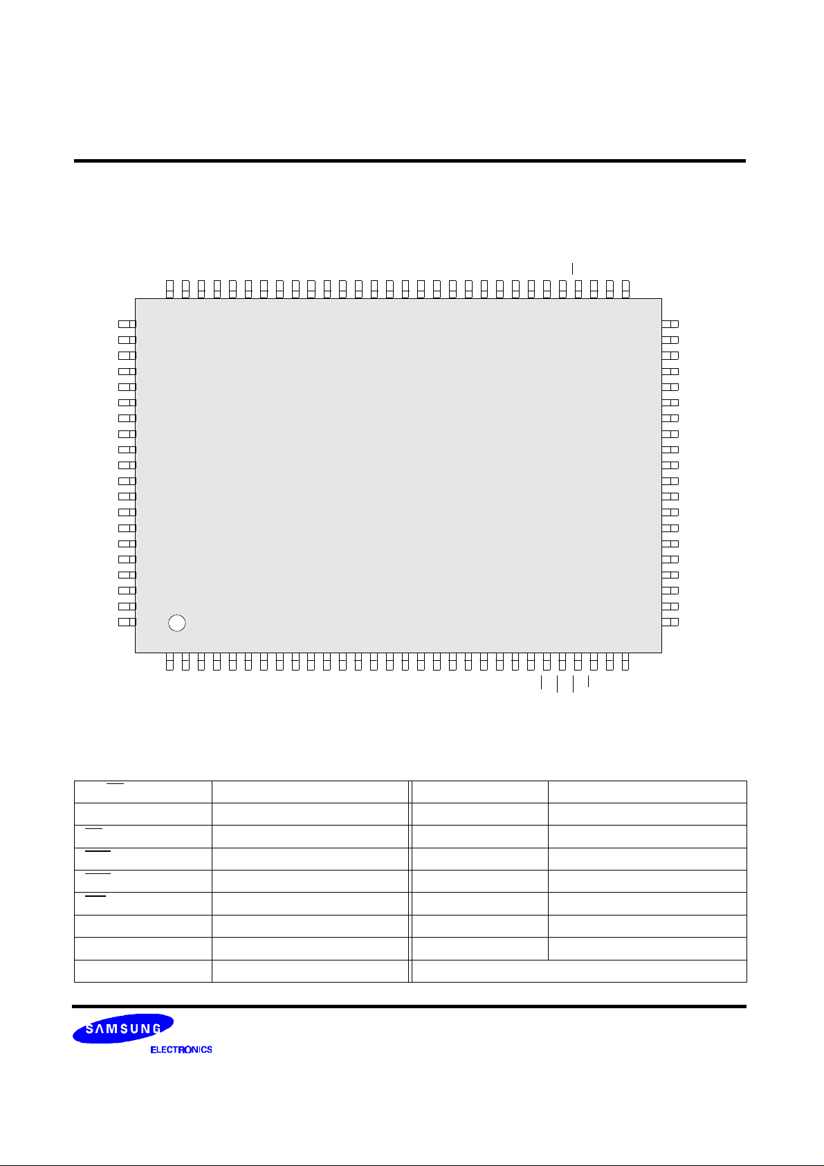
PIN CONFIGURATION (Top View)
DQ28
VDDQ
DQ27
DQ26
VSSQ
DQ25
DQ24
VDDQ
DQ15
DQ14
128M DDR SDRAM
VSSQ
DQ13
DQ12
VDDQ
VSS
VDD
DQ11
DQ10
VSSQ
DQ9
DQ8
VDDQ
VREF
DM3
DM1CKCK
CKE
MCL
A8(AP)
DQ29
VSSQ
DQ30
DQ31
VSS
VDDQ
N.C
N.C
N.C
N.C
N.C
VSSQ
RFU
DQS
VDDQ
VDD
DQ0
DQ1
VSSQ
DQ2
8079787776757473727170696867666564636261605958575655545352
81
82
83
84
85
86
87
88
89
90
91
92
93
94
95
96
97
98
99
100
1234567891011121314151617181920212223242526272829
DQ3
DQ4
DQ5
DQ6
DQ7
VDDQ
VSSQ
DQ16
VDDQ
100 Pin TQFP
20 x 14 mm
0.65mm pin Pitch
DQ17
DQ18
DQ19
VSSQ
VDDQ
2
VSS
VDD
DQ20
DQ21
DQ22
VSSQ
DM0
DQ23
DM2
VDDQ
51
50
A7
49
A6
48
A5
47
A4
46
VSS
45
A9
44
N.C
43
N.C
42
N.C
41
N.C
40
N.C
39
N.C
38
N.C
37
A11
36
A10
35
VDD
34
A3
33
A2
32
A1
31
A0
30
WE
CS
CAS
BA0
RAS
BA1
PIN DESCRIPTION
CK,CK Differential Clock Input BA0, BA1 Bank Select Address
CKE Clock Enable A0 ~A11 Address Input
CS Chip Select DQ0 ~ DQ31 Data Input/Output
RAS Row Address Strobe VDD Power
CAS Column Address Strobe VSS Ground
WE Write Enable VDDQ Power for DQ′s
DQS Data Strobe VSSQ Ground for DQ′s
DMi Data Mask MCL Must Connect Low
RFU Reserved for Future Use
- 5 -
Rev. 1.3 (Aug. 2001)
K4D263238M
128M DDR SDRAM
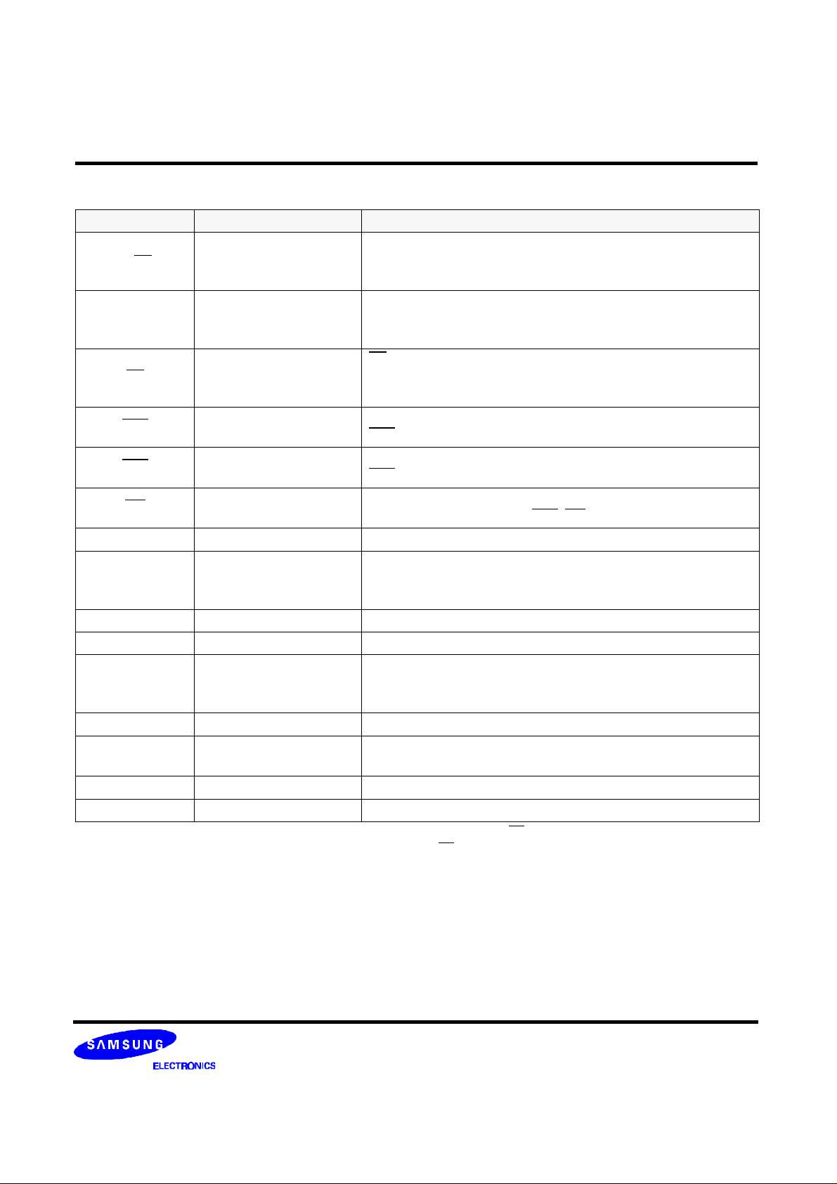
INPUT/OUTPUT FUNCTIONAL DESCRIPTION
Symbol Type Function
The differential system clock Input.
*1
CK, CK
CKE Input
CS Input
RAS Input
CAS Input
WE Input
DQS Input/Output Data input and output are synchronized with both edge of DQS.
DM0 ~ DM3 Input
DQ0 ~ DQ31 Input/Output Data inputs/Outputs are multiplexed on the same pins.
BA0, BA1 Input Selects which bank is to be active.
A0 ~ A11 Input
VDD/VSS Power Supply Power and ground for the input buffers and core logic.
VDDQ/VSSQ Power Supply
VREF Power Supply Reference voltage for inputs, used for SSTL interface.
MCL Must Connect Low Must connect Low
*1 : The timing reference point for the differential clocking is the cross point of CK and CK.
For any applications using the single ended clocking, apply VREF to CK pin.
Input
All of the inputs are sampled on the rising edge of the clock except
DQ′s and DM′s that are sampled on both edges of the DQS.
Activates the CK signal when high and deactivates the CK signal
when low. By deactivating the clock, CKE low indicates the Power
down mode or Self refresh mode.
CS enables the command decoder when low and disabled the command decoder when high. When the command decoder is disabled,
new commands are ignored but previous operations continue.
Latches row addresses on the positive going edge of the CK with
RAS low. Enables row access & precharge.
Latches column addresses on the positive going edge of the CK with
CAS low. Enables column access.
Enables write operation and row precharge.
Latches data in starting from CAS, WE active.
Data In mask. Data In is masked by DM Latency=0 when DM is high
in burst write. DM0 for DQ0 ~ DQ7, DM1 for DQ8 ~ DQ15, DM2 for
DQ16 ~ DQ23, DM3 for DQ24 ~ DQ31.
Row/Column addresses are multiplexed on the same pins.
Row addresses : RA0 ~ RA11, Column addresses : CA0 ~ CA7.
Column address CA8 is used for auto precharge.
Isolated power supply and ground for the output buffers to provide
improved noise immunity.
- 6 -
Rev. 1.3 (Aug. 2001)
 Loading...