

Page 1
7. Flow Chart of Troubleshooting
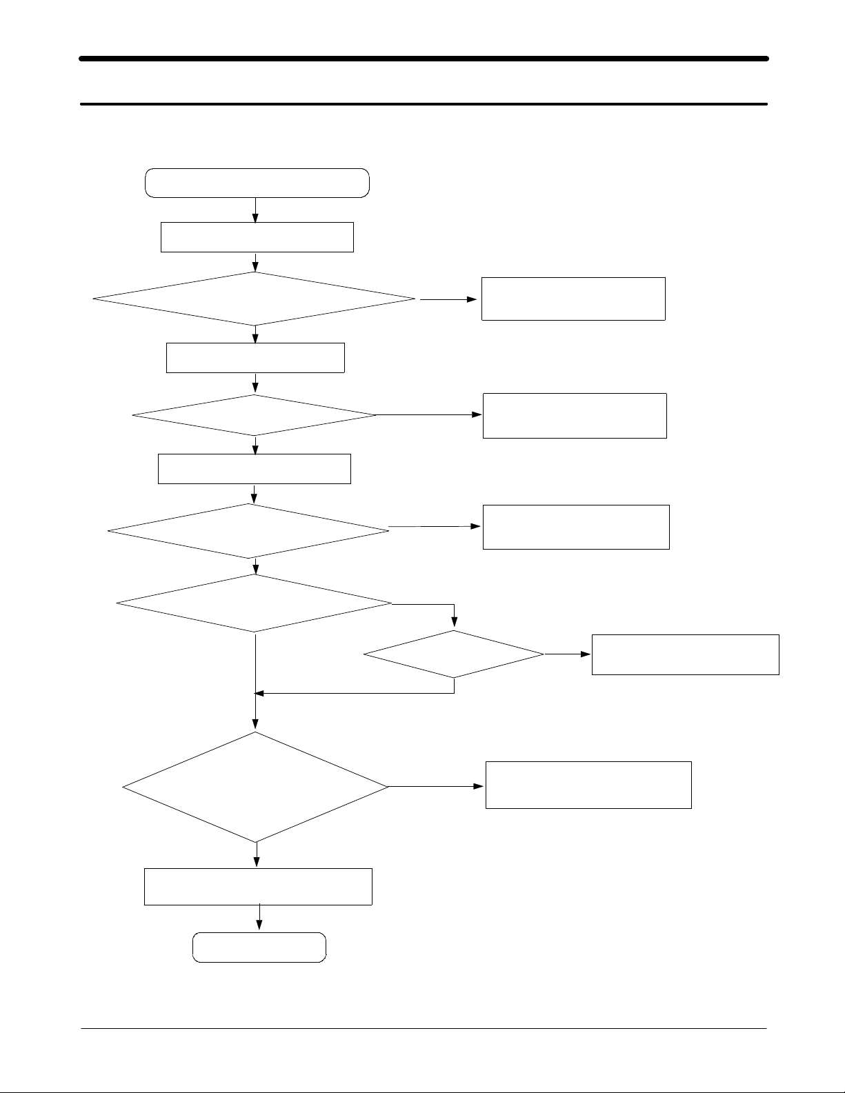
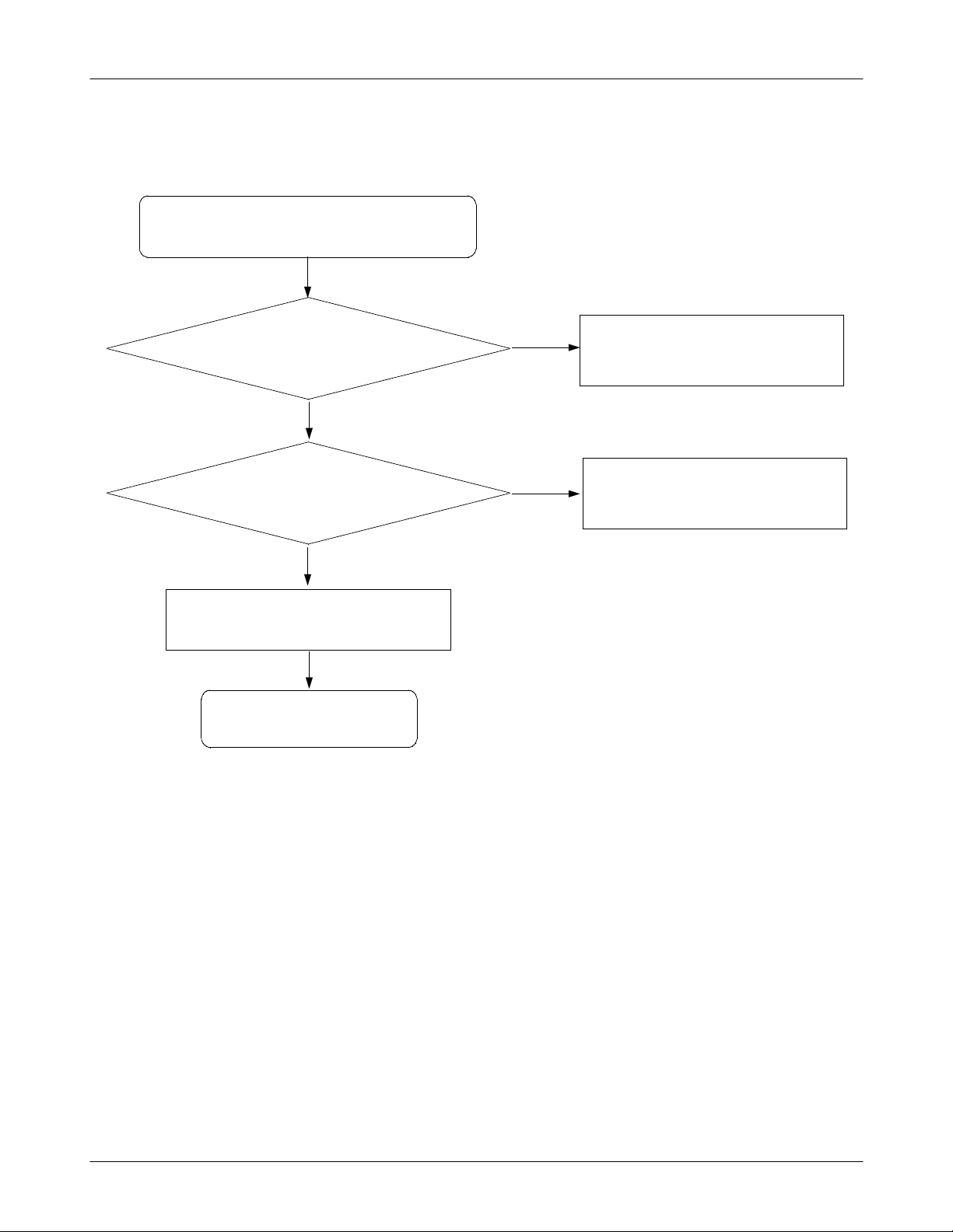
7-1. Power On
The set is not ' Power On '
Check the current consumption
Current consumption
>=100mA
Yes
Check the +VBATT Voltage
Voltage >= 3.3V
Yes
Check the pin of U300
pin#J12 of U300 >= 2.8V
Yes
pin#A13 of U300 = 2.8V
Yes
No
No
No
No
pin#G11 = 1.8V
Download again
Charge the Battery
Check U300 and C314
No
Check U300 and C315
Check the clock signal
at pin#3 of U102
Freq = 26MHz ,
Vrms ≥ 300mV
Yes
Check the initial operation
END
SAMSUNG Proprietary-Contents may change without notice
This Document can not be used without Samsung's authorization
Yes
7-1
No
Check the clock generation circuit
(related to U102)
Page 2
Flow Chart of Troubleshooting
7-2
SAMSUNG Proprietary-Contents may change without notice
This Document can not be used without Samsung's authorization
Page 3
7-2. Initial
Flow Chart of Troubleshooting
Initialization Failure
Yes
The pin#G11 of U300 = 1.8V
the pin#J12 of U300 ≒ 2.825V
Is the pin#K9 of U300
32.768kHz wave forms at
the C216 and C217
The Voltage is "High" at
and
?
Yes
"Low -> High"?
Yes
Yes
the C313
No
No
No
No
(If it has some problem, adjust it.)
(If it has some problem, adjust it.)
Check the U300
Check the U300
Check the U200
Check the U300
Yes
No
LCD display is O.K
Yes
No
Sound is O.K
Yes
END
Check the LCD Part
Check the Audio Part
7-3
SAMSUNG Proprietary-Contents may change without notice
This Document can not be used without Samsung's authorization
Page 4
Flow Chart of Troubleshooting
7-4
SAMSUNG Proprietary-Contents may change without notice
This Document can not be used without Samsung's authorization
Page 5
7-3. SIM Part
"Insert SIM" is displayed on the LCD
Yes
Are there any Signals at
pin#N9, #R10, #P10 of U300?
Yes
Flow Chart of Troubleshooting
No
Check the U200
Are there any Signals at
pin#K12, #K11, #K14, #J11 of
CN100?
Yes
Check the SIM Card
END
No
Check the U300
7-5
SAMSUNG Proprietary-Contents may change without notice
This Document can not be used without Samsung's authorization
Page 6
Flow Chart of Troubleshooting
7-4. Charging Part
Abnormal charging operation
The pin#17, #18 of
CN701 is TA_VEXT ≒
The pin#8 of U301 is 3.2~4.2V ?
The ICHRG = 1.4V(during
charging) and ≒ 180mV(full
5V ?
Yes
Yes
charging) ?
Yes
No
Replace TA or Check CN701
No
Check the U301
No
Solder again or change R310
END
7-6
SAMSUNG Proprietary-Contents may change without notice
This Document can not be used without Samsung's authorization
Page 7
Flow Chart of Troubleshooting
7-7
SAMSUNG Proprietary-Contents may change without notice
This Document can not be used without Samsung's authorization
Page 8

Flow Chart of Troubleshooting
RTX_QN
RTX_QP
RTX_IN
RTX_IP
AOUTAP
AOUTAN
AOUTBP
AOUTBN
MICINP
MICINN
MICOUTP
MICOUTN
AUXINP
AUXINN
AUXOUTP
AUXOUTN
TP305
C322
CLK32K
CLK13M_MC
DSP_INT
JIG_ON
PWR_ON
RST
R309
Q300
2
INTRQ
KEY_ROW(0)
PWR_KEEP
FLASH_RESET
TX_BAND_SEL
TXPOWER
C318
1
SERDAT
SERCLK
AFC
C2
C1
SERCK
SERDA
D9
AFC
E7
TXP
B5
RAREF2
B6
RAREF1
D7
RXTXIP
D6
RXTXIN
C7
RXTXQP
C6
RXTXQN
P11
AOUTAP
N12
AOUTAN
R12
AOUTBP
P12
AOUTBN
N14
MICINP
M14
MICINN
N15
MICOUTP
P15
MICOUTN
M15
AUXINP
L14
AUXINN
K13
AUXOUTP
L13
AUXOUTN
R13
VXVCM
M13
VREGP
R14
VREGN
R4
DAICK
P4
DAIRN
L6
DAIDI
M6
DAIDO
N4
RTC_CLK
D1
XOENAQ
R6
MC
P5
NC7
P3
DINTR
C14
PWR_SW2
C15
PWR_SW1N
L7
PSW1_BUF
K9
RESET_O
N10
MODE
M9
PWR_KEEP
L10
INTRQ
L9
VIB_RNG_EN
RTC_ALMN
CREF
H10
E9
C317
PCS_RX_EN
DSP_RWN
XOENA
SERLE
RF_EN
TX_EN
G6
B1
A2
A4
B3
A3
SERLE1
SERLE2
OCTL5
OCTL6
OCTL7
OCTL4
ADC_AUX1
ADC_AUX2
CH_BDRV
CH_ISEN
CH_RES
VREF
A10
E11
F12
D14
E10
D15
DSP_IO
R302
DSP_AB(0)
DSP_AB(1)
R3
C5
K6
E6
E5
F5
OCTL2
OCTL3
VBAT
VEXT
E14
E13
P1
L2
L3
RWN
RESETN_CSP
OCTL0
OCTL1
I|O
AB0
AB1
SCLK_PSC
SDO_PSC
CSN_PSC
SDI_PSC
VLDO_1
VLDO_2
VACC
G11
F14
N7
L8
M7
K8
DSP_AB(0:8)
DSP_AB(8)
DSP_AB(7)
DSP_AB(6)
DSP_AB(5)
DSP_AB(4)
DSP_AB(3)
DSP_AB(2)
L5
AB2
DSP_DB(1)
DSP_DB(0)
M2
M1
K1
K2
N2
K7
K5
N1
DB0
DB1
AB4
AB5
AB6
AB7
AB8
AB3
DSP_DB(9)
DSP_DB(8)
DSP_DB(7)
DSP_DB(6)
DSP_DB(5)
DSP_DB(4)
DSP_DB(3)
DSP_DB(2)
G3
G4
K3
H5
F4
F1
J5
J6
DB2
DB3
DB4
DB5
DB6
DB7
DB8
DB9
U300
LED1_DRV
LED2_DRV
RING_DRV
VLDO_3
VLDO_4
J12
A13
B12
VIB_DRV
VLDO_5
VLDO_6
VLDO_7
VL5S_A
VL5S_B
VL4S_A
VL4S_B
D10
B10
A12
B11
VRTC
VSIM
H11
C9
K12
A14
C12
F15
F13
G13
G12
3
TP301
DCS_TX_EN
EAR_ADC
KEY_COL(2)
VREF
UP_SDO
UP_SDI
UP_SCLK
GSM_TX_EN
UP_CS
KEY_BL1
DSP_DB(0:15)
DSP_DB(15)
DSP_DB(14)
DSP_DB(13)
DSP_DB(12)
DSP_DB(11)
DSP_DB(10)
D3
D2
E2
E3
F2
F3
DB14
DB15
DB10
DB11
DB12
DB13
2
NC6
1
NC5
K10
GNDS17
J10
GNDS16
J9
GNDS15
J8
GNDS14
J7
GNDS13
H9
GNDS12
H8
GNDS11
H7
GNDS10
H6
GNDS9
G10
GNDS8
G9
GNDS7
G8
GNDS6
G7
GNDS5
F10
GNDS4
F9
GNDS3
F8
GNDS2
F7
GNDS1
D13
AUX_ADC3
B4
SIM_CLK
SIM_RST
K14
K11
GND_OCTL
C4
VDD_OCTL
P13
GNDV
L11
VDDV
F6
GNDB
A6
VDDB
M10
GNDD
N11
VDDD
P6
VSS4
R2
VSS3
K4
VSS2
G5
VSS1
J4
VDD_IO2
N5
VDD_IO1
N6
VDD3
M3
VDD2
J3
VDD1
F11
GND_HCUR
K15
GND_PSC2
B15
GND_PSC1
E8
GNDQ
B13
VDD67
C10
VDD5
UP_CLK
UP_RST
SIM_IO
VDD12
VDD34
UP_IO
P10
R10
J13
C11
J11
N9
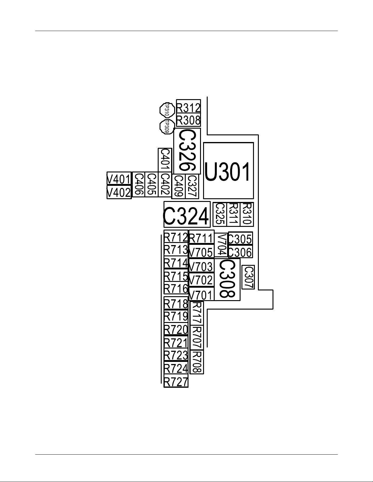
VRF
R300
C301
VCCA
C300
VCCD
C302
VBAT
TP307
TP306
TP308
SIMRST
SIMDATA
SIMCLK
C303
1uF
10V
TA_VEXT
C324 C325
ICHRG CHG_ON
R310
R311
C327
3
2
1
GND
IN 4 ISET
VL
GG
9
10 11
GG
12
_EN
5
C326
U301
_ACOK
_CHG
BATT
6
8
7
TP309
R308
TP310
R312
R303
R304
RTCALARM
VCCD
VCCD
VBAT
C310
VRTC
C316 C313
C311
VBAT
VCCB
VRF
C314
C315 C312
POS
NEG
U303
VCCD VCCA
VCC_1.8A
C309
R301
C304
4 4 5 5 6
6
GG
7
CN300
8
GG
9
10
11
33
2 2
C305
C306
C307
C308
VRTC
CHG_DET
7-8
SAMSUNG Proprietary-Contents may change without notice
This Document can not be used without Samsung's authorization
Page 9

7-5. Microphone Part
Microphone does not work
Is the assembled status of
microphone O.K?
Check the reference voltage on Mic path
Flow Chart of Troubleshooting
Yes
No
Reassemble the microphone
Yes
C410 > 2.5V
Yes
Is microphone ok ?
Yes
END
No
Solder the microphone again or
Replace around Mic Circuit
(C403, C407, R407, R410.....)
No
Check U300
7-9
SAMSUNG Proprietary-Contents may change without notice
This Document can not be used without Samsung's authorization
Page 10

Flow Chart of Troubleshooting
7-10
SAMSUNG Proprietary-Contents may change without notice
This Document can not be used without Samsung's authorization
Page 11

7-6. Speaker Part
There is no sound from Speaker
Flow Chart of Troubleshooting
Yes
The pin#4
of U402 is
No
Is the terminal of Speaker
O.K.?
Yes
Are there any
signals
at the pin#5 and
The type of sound
from the Speaker is
Yes
Melody
No
No
Check U402
No
No
Are there any
signals
at the pin#2 and
YesYes
Replace the Speaker
Yes
The pin#4
of U402 is
No
Check U402
Check U300
END
7-11
SAMSUNG Proprietary-Contents may change without notice
This Document can not be used without Samsung's authorization
Page 12

Flow Chart of Troubleshooting
AOUTBP
R420
VCCD
VBAT
R422
3
1
2
V+
NO1
U402
NO2
COM2
8
9
10
R421
SPK_TP
AOUTBN
RADIO_SHUTDOWN
SPK_TN
EARSPK_R
R424
C420
4
5
11
IN1
G G
NC1
COM1
12 13
G
14
G
NC2
GND
IN2
6
7
R423
EARSPK_L
CN400
2 2
4 4
11
33
55
EARPIECE
C421
R_ANT
SPK_TP
14
GG
12 13
8 8
10
6 6
GG
11
99
77
10
L403
C422
SPK_TN
R425
MIC+
V401
C401
C402
L401
C400
R401
MIC
MIC1
R416
VCCD
V402
C406
C409
C405
R406
L402
R405
C403
C407
R402
C404
R407
VCCA
C408
R403
R408
0
R411
2.7K
R410
R409
C410
C411
C412
R412
VCCD
C415
C414
C413
1
5
4
C417
C416
R415
R419
VCCD
R418
C418
R417
3
2
U401
EAR_SWITCH
C419
V405
V404
V403
JACK_IN
EAR_ADC
R413
R400
MICINP
MICOUTP
R404
MICINN
MICOUTN
AUXINP
AUXOUTP
R414
AUXINN
AUXOUTN
7-12
SAMSUNG Proprietary-Contents may change without notice
This Document can not be used without Samsung's authorization
Page 13

7-8. EGSM Reciever
CONTINUOUS RX ON
RF INPUT : 62CH
AMP : -50dBm
Flow Chart of Troubleshooting
NORMAL CONDITION
catch the channel?
NO
F100 CHECK
pin#9 ≥ -65dBm ?
YES
F100 CHECK
pin#11 ≥ -65dBm ?
YES
U100 CHECK
pin#21,22 ≥ -65dBm ?
YES
U100 CHECK
pin#31 : 26MHz ?
Vp-p : 860mV?
NO
YES
NO
NO
NO
Check soldered status of
C108, L111, L102
CN100
resolder or change
F100, C127, L108
resolder or change
C131,C132,L109
resolder or change
U102 CHECK
26MHz ?
Vp-p : 950mV?
NO
U102 CHECK
clean 3V?
YES
CHECK
U300
7-13
SAMSUNG Proprietary-Contents may change without notice
This Document can not be used without Samsung's authorization
YES
U102
Resolder or
Change?
Page 14

Flow Chart of Troubleshooting
7-9. EGSM transmitter
F100 pin#7 :
about 2~3
dBm?
YES
CN100, C105
check&change
C109 : 3.7 V?
U101 : 1.2V?
NO
YES
Between
R101 &
NO
F100
pin#4 : 3 V?
YES
C106
≒ 4~5dBm?
YES
U101
check & change
NO
BATTERY, U100
check & change
NO
NO
check & change
U300
R101
check &
change
CONTINUS TX ON CONDITION
TX POWER DAC:500 CODE APPLIED
NO
CH:62
RBW : 100KHz
VBW : 100KHz
SPAN : 10MHz
REF LEV. : 10dBm
ATT. : 20dB
U300
check &
NO
U100
change or
resolder
YES
R102 :
≒ -5dBm ?
YES
U101
change
YES
7-14
SAMSUNG Proprietary-Contents may change without notice
This Document can not be used without Samsung's authorization
Page 15

7-10. DCS Receiver
CONTINUOUS RX ON
RF INPUT : 698CH
AMP : -50dBm
Flow Chart of Troubleshooting
NORMAL CONDITION
catch the channel?
NO
F100 CHECK
pin#9 ≥ -65dBm ?
YES
F100 CHECK
pin#1 ≥ -65dBm ?
YES
U100 CHECK
pin#19,20 ≥ -65dBm ?
YES
U100 CHECK
pin#31 : 26MHz ?
Vp-p : 860mV?
NO
YES
NO
NO
NO
Check soldered status of
C108, L111, L102
CN100
resolder or change
F100, C130, L110
resolder or change
C129, C128, L107
resolder or change
U102 CHECK
26MHz ?
Vp-p : 950mV?
NO
U102 CHECK
clean 3V?
YES
CHECK
U300
7-15
SAMSUNG Proprietary-Contents may change without notice
This Document can not be used without Samsung's authorization
YES
U102
Resolder or
Change?
Page 16

Flow Chart of Troubleshooting
7-11. DCS transmitter
F100 pin#5 :
about 2~3
dBm?
YES
CN100, C105
check&change
C109 : 3.7 V?
NO
NO
YES
Between
R101 & U101
: 1.2V?
F100
pin#10 : 3 V?
YES
L101:
≒ 4~5dBm?
YES
U101
check & change
NO
BATTERY, U100
check & change
NO
NO
check & change
U300
R101
check &
change
CONTINUOUS TX ON CONDITION
CH : 698CH(DCS),660CH(PCS)
TX POWER CODE: 350 CODE APPLIED
RBW : 100KHz
VBW : 100KHz
SPAN : 10MHz
REF LEV. : 10dBm
ATT. : 20dB
NO
U300
check
NO
U100
change or
resolder
YES
R100:
≒ -5dBm ?
YES
U101
change or
resolder
YES
7-16
SAMSUNG Proprietary-Contents may change without notice
This Document can not be used without Samsung's authorization
Page 17

7-12. PCS Receiver
CONTINUOUS RX ON
RF INPUT : 698CH
AMP : -50dBm
Flow Chart of Troubleshooting
NORMAL CONDITION
catch the channel?
NO
F100 CHECK
pin#9 ≥ -65dBm ?
YES
F100 CHECK
pin#3 ≥ -65dBm ?
YES
U100 CHECK
pin#17,18 ≥ -65dBm ?
YES
U100 CHECK
pin#31 : 26MHz ?
Vp-p : 860mV?
NO
YES
NO
NO
NO
Check soldered status of
C108, L111, L102
CN100
resolder or change
F100, C125, L106
resolder or change
C126, C124, L105
resolder or change
U102 CHECK
26MHz ?
Vp-p : 950mV?
NO
U102 CHECK
clean 3V?
YES
CHECK
U300
7-17
SAMSUNG Proprietary-Contents may change without notice
This Document can not be used without Samsung's authorization
YES
U102
Resolder or
Change?
Page 18

Flow Chart of Troubleshooting
7-13. PCS transmitter
F100 pin#5 :
about 2~3
dBm?
YES
CN100, C105
check&change
C109 : 3.7 V?
NO
NO
YES
Between
R101 & U101
: 1.2V?
F100
pin#10 : 3 V?
YES
L101:
≒ 4~5dBm?
YES
U101
check & change
NO
BATTERY, U100
check & change
NO
NO
check & change
U300
R101
check &
change
CONTINUOUS TX ON CONDITION
CH : 698CH(DCS),660CH(PCS)
TX POWER CODE: 350 CODE APPLIED
RBW : 100KHz
VBW : 100KHz
SPAN : 10MHz
REF LEV. : 10dBm
ATT. : 20dB
NO
U300
check
NO
U100
change or
resolder
YES
R100:
≒ -5dBm ?
YES
U101
change or
resolder
SAMSUNG Proprietary-Contents may change without notice
YES
7-18
This Document can not be used without Samsung's authorization
Page 19

Flow Chart of Troubleshooting
7-19
SAMSUNG Proprietary-Contents may change without notice
This Document can not be used without Samsung's authorization
Page 20

Flow Chart of Troubleshooting
GSM_PAM_IN
R102
TXPOWER
R101
C110
C113
C114
C115
C116
C117
C109
6
7
4
5
VRAMP
GSM_IN
VBATT
CEXT
VCC2
8
9
G
GSM_OUT
TX_EN
VCC_OUT
G
G
13
12
11
10
TX_BAND_SEL
TX_EN
VBAT
C104
C103
3
2
1
BS
DCS/PCS_IN
19
G
VCC2
DCS/PCS_OUT
18
17
G
16 G 15 G 14
DCS_PAM_IN
R100 0
U101
C111
L103
3.9nH
C112
DCSRX
5
DCS_RX
DCS|PCSTX
14
G G
13
G
12
G
86
G
EGSM_RX
EGSM_TX
11
2 VC3
7
EGSMRX
PCS_RX_EN
C106 C108
L101
C107
PCSRX
3
1
PCS_RX
L112
6
G G
5
CN100
G
ANT
9
VC2 4
F100
10 VC1
DCS_TX_EN
GSM_TX_EN
4
3
C105
A C
2
G
1
C137
L102
TP103
ANT101 ANT100
7-20
SAMSUNG Proprietary-Contents may change without notice
This Document can not be used without Samsung's authorization
Page 21

Flow Chart of Troubleshooting
SERDAT
XOENA
U102
4
1
3
2
C133
C136
R105
SERCLK
NC
35
SCLK 1 SDIO
NC
GND
33 34
XEN
32
XTAL1
31
XTAL2
30
VDD
29
28
VDD
AFC
27
XDIV
26
RFIAN 24
XMODE
25
RTX_QN
SERLE
_SEN
RTX_QP
2
3
4
BQN 5 BQP
U100
RFIDN
RFIAP
RFIEN
RFIEP
23
20
22
21
13MHZ_BB
RTX_IN
RTX_IP
8
6
7
XOUT
BIN
BIP
_PDN
_RESET
VIO
VDD
VDD
GND
RFOL
RFOH
RFIPP
RFIDP
RFIPN
19
18
17
RF_EN
C123
9
10
11
12
13
14
15
16
VCCD
C120
VRF
VRF
AFC
13MHZ_BB
R103
R107
0
R106
R104
C134
C135
CLK13M_YMU
CLK13M_TR
CLK13M_MC
(MURATA)
L109
C132
6
OUT
OUT 7 OUT 8 OUT
F102
IN
DCS
L110
DCSRX
(MURATA)
L107
C129
C131
IN
1
C128
9
10
G G
3 5
G G
2
4
GSM
L108
C130
C127
EGSMRX
(MURATA)
L105
C126
C124
C122
C121
3
4
OUT
OUT
F101
5
G G
2
IN
1
L106
C125
DCS_PAM_IN
PCSRX
GSM_PAM_IN
7-21
SAMSUNG Proprietary-Contents may change without notice
This Document can not be used without Samsung's authorization
Page 22

Flow Chart of Troubleshooting
7-22
SAMSUNG Proprietary-Contents may change without notice
This Document can not be used without Samsung's authorization
 Loading...