


AOD4184A
40V N-Channel MOSFET
General Description
The AOD4184A combines advanced trench MOSFET technology with a low resistance package to provide extremely low RDS(ON). This device is well suited for high current load applications.
Product Summary
VDS |
40V |
ID (at VGS=10V) |
50A |
RDS(ON) (at VGS=10V) |
< 7mΩ |
RDS(ON) (at VGS = 4.5V) |
< 9.5mΩ |
100% UIS Tested |
|
100% Rg Tested |
|
|
|
|
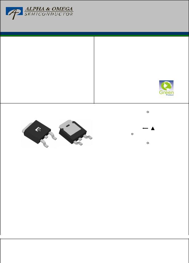
TO252 |
|
|
|
|
|
|
|
|
|
|
|
|
|
|
|
DPAK |
|
|
|
|
|
|
|
D |
||||
|
Top View |
Bottom View |
|
|
|
|
|
|
|
|
|
|
|||
D |
|
|
D |
|
|
|
|
|
|
|
|
|
|
|
|
|
|
|
|
|
|
|
|
|
|
|
|
|
|
||
|
|
|
|
|
|
|
|
|
|
|
|
|
|
|
|
|
|
|
|
|
|
|
|
|
|
|
|
|
|
|
|
|
|
|
|
|
|
|
|
|
|
|
|
|
|
|
|
|
|
|
|
|
|
|
|
|
|
|
|
|
|
|
|
|
|
|
|
|
|
|
|
|
|
|
|
|
|
|
|
|
|
|
|
|
|
|
G |
|
|
|
|
|
|||
|
|
|
|
|
|
|
|
|
|
|
|
||||
|
|
|
S |
|
|
G |
S |
||||||||
|
|
|
G |
|
S |
|
|
|
|
|
|||||
|
|
|
|
|
|
|
|
|
|
|
|
|
|
||
|
|
|
|
|
|
|
|
|
|
|
|
|
|
|
|
|
|
|
|
|
|
|
|
|
|||||||
Absolute Maximum Ratings TA=25°C unless otherwise noted |
|
|
|
|
|
||||||||||
Parameter |
|
|
|
|
Symbol |
|
Maximum |
|
|
|
|
Units |
|||
Drain-Source Voltage |
|
|
VDS |
|
40 |
|
|
|
|
|
|
|
V |
||
Gate-Source Voltage |
|
|
VGS |
|
±20 |
|
|
|
|
|
|
|
V |
||
Continuous Drain |
|
|
TC=25°C |
|
ID |
|
50 |
|
|
|
|
|
|
|
|
Current G |
|
|
TC=100°C |
|
|
40 |
|
|
|
|
|
|
|
A |
|
Pulsed Drain Current C |
|
|
|
IDM |
|
120 |
|
|
|
|
|
|
|
|
|
Continuous Drain |
|
|
TA=25°C |
|
IDSM |
|
13 |
|
|
|
|
|
|
|
A |
Current |
|
|
TA=70°C |
|
|
10 |
|
|
|
|
|
|
|
||
|
|
|
|
|
|
|
|
|
|
|
|
|
|||
Avalanche Current C |
|
|
|
IAS, IAR |
|
35 |
|
|
|
|
|
|
|
A |
|
Avalanche energy L=0.1mH C |
|
EAS, EAR |
|
61 |
|
|
|
|
|
|
|
mJ |
|||
|
B |
|
TC=25°C |
|
PD |
|
50 |
|
|
|
|
|
|
|
W |
Power Dissipation |
|
TC=100°C |
|
|
25 |
|
|
|
|
|
|
|
|||
|
|
|
|
|
|
|
|
|
|
|
|
|
|||
|
A |
|
TA=25°C |
|
PDSM |
|
2.3 |
|
|
|
|
|
|
|
W |
Power Dissipation |
|
TA=70°C |
|
|
1.5 |
|
|
|
|
|
|
|
|||
|
|
|
|
|
|
|
|
|
|
|
|
|
|||
Junction and Storage Temperature Range |
TJ, TSTG |
|
-55 to 175 |
|
|
|
|
°C |
|||||||
Thermal Characteristics
Parameter |
|
Symbol |
Typ |
Max |
Units |
|
Maximum Junction-to-Ambient A |
t ≤ 10s |
RθJA |
18 |
22 |
°C/W |
|
Maximum Junction-to-Ambient A D |
Steady-State |
44 |
55 |
°C/W |
||
|
||||||
Maximum Junction-to-Case |
Steady-State |
RθJC |
2.4 |
3 |
°C/W |
Rev0 : Sep 2009 |
www.aosmd.com |
Page 1 of 6 |
AOD4189
P-Channel Enhancement Mode Field Effect Transistor
General Description |
|
|
|
Features |
|
|
|
|
|
|
|
|
The AOD4189 uses advanced trench technology and |
|
VDS (V) = -40V |
|
|
|
|
|
|
|
|
||
design to provide excellent RDS(ON) with low gate |
|
ID = -40A |
(VGS = -10V) |
|||||||||
charge. With the excellent thermal resistance of the |
|
RDS(ON) < 22mΩ |
(VGS = -10V) |
|||||||||
DPAK package, this device is well suited for high |
|
RDS(ON) < 29mΩ |
(VGS = -4.5V) |
|||||||||
current load applications. |
|
|
|
|||||||||
|
|
|
|
|
|
|
|
|
|
|
|
|
-RoHS Compliant |
|
|
|
100% UIS Tested! |
||||||||
|
|
|
100% Rg Tested! |
|||||||||
-Halogen Free* |
|
|
|
|||||||||
|
|
|
|
|
|
|
|
|
|
|
|
|
|
|
|
|
|
|
|
|
|
|
|
|
|
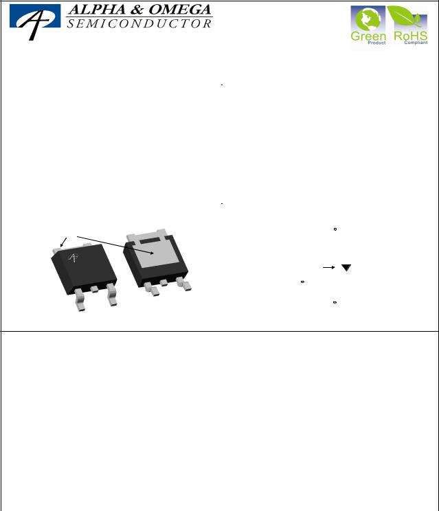
TO-252 |
|
|
|
|
|
|
|
|
|
|
|
|
D-PAK |
Bottom View |
|
|
|
|
|
|
|
|
|
|
|
Top View |
|
|
|
|
|
|
|
|
D |
|||
|
|
|
|
|
|
|
|
|
||||
|
|
|
|
|
|
|
|
|
|
|||
D |
|
|
|
|
|
|
|
|
|
|
|
|
|
S |
G |
|
|
G |
|
|
|
|
|
||
|
|
|
|
|
|
|
|
|
||||
|
|
|
|
|
|
|
|
|
||||
|
|
|
|
|
|
|
|
|||||
|
|
|
|
|
|
|
|
|
||||
|
|
|
|
|
|
|
|
|
||||
|
|
|
|
|
|
|
|
|
||||
|
|
|
|
|
|
|
|
|
||||
|
|
|
|
|
|
|
|
|
||||
|
|
|
|
|
|
|
|
|
|
|
||
|
|
|
|
|
|
|
S |
|||||
|
|
|
|
|
|
|
|
|||||
GS
Absolute Maximum Ratings TC=25°C unless otherwise noted
Parameter |
|
|
|
|
Symbol |
|
Maximum |
|
Units |
Drain-Source Voltage |
|
|
|
|
VDS |
|
-40 |
|
V |
Gate-Source Voltage |
|
|
|
|
VGS |
|
±20 |
|
V |
Continuous Drain |
TC=25°C |
|
|
|
|
-40 |
|
|
|
Current B,H |
TC=100°C |
|
|
ID |
|
-28 |
|
A |
|
Pulsed Drain CurrentC |
|
|
|
|
IDM |
|
-50 |
|
|
|
|
|
|
|
|
|
|||
Avalanche Current C |
|
|
|
|
IAR |
|
-35 |
|
|
Repetitive avalanche energy L=0.1mH C |
|
|
E |
|
61 |
|
mJ |
||
|
|
|
|
|
AR |
|
|
|
|
|
TC=25°C |
|
|
PD |
|
62.5 |
|
|
|
Power Dissipation B |
TC=100°C |
|
|
|
31 |
|
W |
||
|
|
|
|
|
|||||
|
TA=25°C |
|
|
PDSM |
|
2.5 |
|
||
|
|
|
|
|
|
||||
Power Dissipation A |
TA=70°C |
|
|
|
1.6 |
|
|
||
|
|
|
|
|
|
||||
Junction and Storage Temperature Range |
|
TJ, TSTG |
|
-55 to 175 |
|
°C |
|||
|
|
|
|
|
|
|
|
|
|
Thermal Characteristics |
|
|
|
|
|
|
|
||
Parameter |
|
|
|
|
|
Symbol |
Typ |
Max |
Units |
Maximum Junction-to-Ambient A,G |
|
|
t ≤ 10s |
RθJA |
15 |
20 |
°C/W |
||
Maximum Junction-to-Ambient A,G |
|
Steady-State |
41 |
50 |
°C/W |
||||
Maximum Junction-to-Case D,F |
|
Steady-State |
RθJC |
2 |
2.4 |
°C/W |
|||
Alpha & Omega Semiconductor, Ltd. |
www.aosmd.com |
 Loading...