


Off-Line PWM Controllers with Integrated Power MOSFET
STR-W6000S Series
General Descriptions
The STR-W6000S series are power ICs for switching power supplies, incorporating a MOSFET and a current mode PWM controller IC.
The low standby power is accomplished by the automatic switching between the PWM operation in normal operation and the burst-oscillation under light load conditions. The product achieves high cost-performance power supply systems with few external components.
Features
Current Mode Type PWM Control
Brown-In and Brown-Out function
Auto Standby Function
No Load Power Consumption < 30 mW
Operation Mode |
|
Normal Operation |
----------------------------- PWM Mode |
Standby ---------------------------- |
Burst Oscillation Mode |
Random Switching Function
Slope Compensation Function
Leading Edge Blanking Function
Bias Assist Function
Audible Noise Suppression function during Standby mode
Protections
Overcurrent Protection (OCP); Pulse-by-Pulse, built-in compensation circuit to minimize OCP point variation on AC input voltage
Overload Protection (OLP); auto-restartOvervoltage Protection (OVP); auto-restartThermal Shutdown Protection (TSD); auto-restart
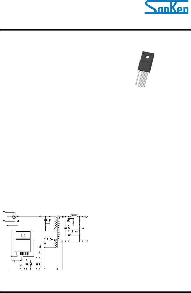
Typical Application Circuit |
|
|
|
|||||||
BR1 |
|
|
|
|
|
|
|
D51 |
L51 |
|
|
|
|
|
|
|
T1 |
|
VOUT(+) |
||
VAC |
|
|
|
|
|
|
|
|
|
|
|
|
|
|
|
|
|
|
|
|
|
|
C1 |
|
|
|
|
C6 |
R1 |
|
|
R54 |
|
|
|
|
|
|
|
|
|||
|
|
|
|
|
|
|
|
|
PC1 |
R51 |
|
|
|
|
|
|
|
|
|
|
|
|
|
|
|
|
|
|
P |
|
|
R55 |
|
|
|
|
|
|
|
|
C51 |
|
|
|
|
|
|
|
|
|
|
|
|
|
|
|
|
|
|
|
D1 |
|
S |
R52 |
C53 |
|
|
|
|
|
|
|
|
|
||
U1 |
|
|
|
|
|
|
|
|
C52 |
R53 |
|
|
|
|
|
|
D2 |
R2 |
|
U51 |
R56 |
|
|
|
|
|
|
|
|
|
|
|
STR-W6000S |
C2 |
D |
|
|
VOUT(-) |
|||||
D/ST |
2 S/OCP |
VCC |
GND FB/OLP BR |
|
|
|
|
|||
RA |
|
|
|
|
||||||
1 |
3 |
4 |
5 |
6 |
7 |
RB |
|
|
|
|
|
|
|
|
|
||||||
C5 |
|
|
|
|
C3 |
C4 |
|
|
|
|
|
|
|
|
|
RC |
|
|
|
|
|
ROCP |
|
|
|
|
|
|
|
|
||
|
|
|
|
PC1 |
|
|
|
|
||
|
|
|
|
|
|
CY |
|
|
|
|
|
|
|
|
|
|
|
|
|
|
|
|
|
|
|
|
|
|
|
|
|
TC_STR-W6000S_1_R1 |
Package
TO220F-6L
Not to Scale
Lineup
Electrical Characteristics
fOSC(AVG) = 67 kHz
|
Products |
|
VDSS |
RDS(ON) |
|
|
(min.) |
(max.) |
|
|
|
|
||
|
STR-W6051S |
|
|
3.95 Ω |
|
|
|
|
|
|
STR-W6052S |
|
650 V |
2.8 Ω |
|
|
|
|
|
|
STR-W6053S |
|
|
1.9 Ω |
|
|
|
|
|
|
STR-W6072S |
|
800 V |
3.6 Ω |
|
|
|
|
|
Output Power, POUT* |
|
|
||
|
Products |
|
POUT (Open frame) |
|
|
|
AC230V |
AC85~265V |
|
|
|
|
||
|
|
|
|
|
|
STR-W6051S |
|
45 W |
30 W |
|
|
|
|
|
|
STR-W6052S |
|
60 W |
40 W |
|
|
|
|
|
|
STR-W6053S |
|
90 W |
60 W |
|
|
|
|
|
|
STR-W6072S |
|
50 W |
32 W |
|
|
|
|
|
*The output power is actual continues power that is measured at 50 °C ambient. The peak output power can be 120 to 140 % of the value stated here. Core size, ON Duty, and thermal design affect the output power. It may be less than the value stated here.
Applications
White goods
Office automation equipment
Industrial equipment
STR-W6000S - DS Rev.2.0 |
SANKEN ELECTRIC CO.,LTD. |
1 |
Aug. 07, 2014 |
http://www.sanken-ele.co.jp/en/ |
|

STR-W6000S Series
|
|
CONTENTS |
|
General Descriptions----------------------------------------------------------------------- |
1 |
||
1. |
Absolute Maximum Ratings--------------------------------------------------------- |
3 |
|
2. |
Electrical Characteristics ------------------------------------------------------------ |
4 |
|
3. |
Performance Curves ------------------------------------------------------------------ |
5 |
|
|
3.1 |
Derating Curves--------------------------------------------------------------- |
5 |
|
3.2 |
Ambient Temperature versus Power Dissipation Curves------------ |
6 |
|
3.3 |
MOSFET Safe Operating Area Curves ---------------------------------- |
7 |
|
3.4 |
Transient Thermal Resistance Curves ----------------------------------- |
8 |
4. |
Functional Block Diagram----------------------------------------------------------- |
9 |
|
5. |
Pin Configuration Definitions------------------------------------------------------- |
9 |
|
6. |
Typical Application Circuit -------------------------------------------------------- |
10 |
|
7. |
Package Outline----------------------------------------------------------------------- |
11 |
|
8. |
Marking Diagram -------------------------------------------------------------------- |
11 |
|
9. |
Operational Description------------------------------------------------------------- |
12 |
|
|
9.1 |
Startup Operation ----------------------------------------------------------- |
12 |
|
9.2 |
Undervoltage Lockout (UVLO)------------------------------------------- |
13 |
|
9.3 |
Bias Assist Function --------------------------------------------------------- |
13 |
|
9.4 |
Constant Output Voltage Control---------------------------------------- |
13 |
|
9.5 |
Leading Edge Blanking Function ---------------------------------------- |
14 |
|
9.6 |
Random Switching Function ---------------------------------------------- |
14 |
|
9.7 |
Automatic Standby Mode Function-------------------------------------- |
14 |
|
9.8 |
Brown-In and Brown-Out Function ------------------------------------- |
15 |
|
9.9 |
Overcurrent Protection Function (OCP) ------------------------------- |
16 |
|
9.10 |
Overload Protection Function (OLP) ----------------------------------- |
17 |
|
9.11 |
Overvoltage Protection (OVP) -------------------------------------------- |
18 |
|
9.12 |
Thermal Shutdown Function (TSD) ------------------------------------- |
18 |
10. |
Design Notes --------------------------------------------------------------------------- |
18 |
|
|
10.1 |
External Components ------------------------------------------------------- |
18 |
|
10.2 |
PCB Trace Layout and Component Placement ----------------------- |
20 |
11. |
Pattern Layout Example ------------------------------------------------------------ |
22 |
|
12. |
Reference Design of Power Supply ----------------------------------------------- |
23 |
|
OPERATING PRECAUTIONS -------------------------------------------------------- |
25 |
||
IMPORTANT NOTES ------------------------------------------------------------------- |
26 |
||
STR-W6000S - DS Rev.2.0 |
SANKEN ELECTRIC CO.,LTD. |
2 |
Aug. 07, 2014 |
|
|

STR-W6000S Series
1.Absolute Maximum Ratings
The polarity value for current specifies a sink as "+," and a source as "−," referencing the IC. |
|
||||||
Unless otherwise specified |
TA = 25 °C |
|
|
|
|
||
Parameter |
|
Symbol |
Test Conditions |
Pins |
Rating |
Units |
Notes |
|
|
|
|
|
|
|
|
|
|
|
|
|
5.0 |
|
STR-W6051S |
|
|
|
|
|
|
|
|
Drain Peak Current(1) |
|
IDPEAK |
Single pulse |
1 – 3 |
7.0 |
A |
STR-W6052S |
|
|
|
|||||
|
7.5 |
STR-W6072S |
|||||
|
|
|
|
|
|
||
|
|
|
|
|
|
|
|
|
|
|
|
|
9.5 |
|
STR-W6053S |
|
|
|
|
|
|
|
|
|
|
|
|
|
5.0 |
|
STR-W6051S |
|
|
|
|
|
|
|
|
Maximum Switching |
|
IDMAX |
Single pulse |
1 – 3 |
7.0 |
A |
STR-W6052S |
|
|
|
|||||
Current(2) |
|
Ta= ‒20 to 125°C |
7.5 |
STR-W6072S |
|||
|
|
|
|
|
|
||
|
|
|
|
|
|
|
|
|
|
|
|
|
9.5 |
|
STR-W6053S |
|
|
|
|
|
|
|
|
|
|
|
ILPEAK=2.0A |
|
47 |
|
STR-W6051S |
|
|
|
|
|
|
|
|
Avalanche Energy(3)(4) |
|
EAS |
ILPEAK=2.3A |
1 – 3 |
60 |
mJ |
STR-W6072S |
|
|
|
|
||||
|
ILPEAK=2.3A |
62 |
STR-W6052S |
||||
|
|
|
|
|
|||
|
|
|
|
|
|
|
|
|
|
|
ILPEAK=2.7A |
|
86 |
|
STR-W6053S |
|
|
|
|
|
|
|
|
S/OCP Pin Voltage |
|
VOCP |
|
3 – 5 |
− 2 to 6 |
V |
|
|
|
|
|
|
|
|
|
VCC Pin Voltage |
|
VCC |
|
4 – 5 |
32 |
V |
|
|
|
|
|
|
|
|
|
FB/OLP Pin Voltage |
|
VFB |
|
6 – 5 |
− 0.3 to 14 |
V |
|
|
|
|
|
|
|
|
|
FB/OLP Pin Sink Current |
|
IFB |
|
6 – 5 |
1.0 |
mA |
|
|
|
|
|
|
|
|
|
BR Pin Voltage |
|
VBR |
|
7 – 5 |
− 0.3 to 7 |
V |
|
|
|
|
|
|
|
|
|
BR Pin Sink Current |
|
IBR |
|
7 – 5 |
1.0 |
mA |
|
|
|
|
|
|
|
|
|
|
|
|
|
|
22.3 |
|
STR-W6051S |
|
|
|
|
|
|
|
|
|
|
|
With infinite |
1 – 3 |
23.6 |
W |
STR-W6052S |
MOSFET Power |
|
|
|
|
|||
|
PD1 |
heatsink |
25.8 |
STR-W6072S |
|||
|
|
|
|||||
Dissipation(5) |
|
|
|
|
|||
|
|
|
|
|
26.5 |
|
STR-W6053S |
|
|
|
|
|
|
|
|
|
|
|
Without heatsink |
1 – 3 |
1.3 |
W |
|
|
|
|
|
|
|
|
|
Control Part Power |
|
PD2 |
VCC×ICC |
4 – 5 |
0.13 |
W |
|
Dissipation |
|
|
|||||
|
|
|
|
|
|
|
|
Internal Frame Temperature |
|
TF |
|
− |
− 20 to 115 |
°C |
|
in Operation |
|
|
|
||||
|
|
|
|
|
|
|
|
Operating Ambient |
|
TOP |
|
− |
− 20 to 115 |
°C |
|
Temperature |
|
|
|
||||
|
|
|
|
|
|
|
|
Storage Temperature |
|
Tstg |
|
− |
− 40 to 125 |
°C |
|
|
|
|
|
|
|
|
|
Junction Temperature |
|
Tch |
|
− |
150 |
°C |
|
|
|
|
|
|
|
|
|
(1)Refer to 3.3 MOSFET Safe Operating Area Curves.
(2)The maximum switching current is the drain current determined by the drive voltage of the IC and threshold voltage (Vth) of the MOSFET.
(3)Refer to Figure 3-2 Avalanche Energy Derating Coefficient Curve.
(4)Single pulse, VDD = 99 V, L = 20 mH
(5)Refer to 3.2 Ta-PD1curves.
STR-W6000S - DS Rev.2.0 |
SANKEN ELECTRIC CO.,LTD. |
3 |
Aug. 07, 2014 |
|
|

STR-W6000S Series
2.Electrical Characteristics
The polarity value for current specifies a sink as "+," and a source as "−," referencing the IC.
Unless otherwise specified, TA = 25 °C, VCC = 18 V
|
Parameter |
Symbol |
Test |
Pins |
Min. |
Typ. |
Max. |
Units |
Notes |
|
|
Conditions |
|||||||||
|
|
|
|
|
|
|
|
|
|
|
|
Power Supply Startup Operation |
|
|
|
|
|
|
|
||
|
|
|
|
|
|
|
|
|
|
|
|
Operation Start Voltage |
VCC(ON) |
|
4 – 5 |
13.8 |
15.3 |
16.8 |
V |
|
|
|
|
|
|
|
|
|
|
|
|
|
|
Operation Stop Voltage(1) |
VCC(OFF) |
|
4 – 5 |
7.3 |
8.1 |
8.9 |
V |
|
|
|
Circuit Current in Operation |
|
ICC(ON) |
VCC = 12 V |
4 – 5 |
− |
− |
2.5 |
mA |
|
|
|
|
|
|
|
|
|
|
|
|
|
Startup Circuit Operation |
VST(ON) |
|
4 – 5 |
− |
40 |
− |
V |
|
|
|
Voltage |
|
|
|||||||
|
|
|
|
|
|
|
|
|
|
|
|
Startup Current |
ISTARTUP |
VCC = 13.5 V |
4 – 5 |
− 3.9 |
− 2.5 |
− 1.1 |
mA |
|
|
|
|
|
|
|
|
|
|
|
|
|
|
Startup Current Biasing |
VCC(BIAS) |
ICC |
4 – 5 |
8.5 |
9.5 |
10.5 |
V |
|
|
|
Threshold Voltage |
= − 100 µA |
|
|||||||
|
|
|
|
|
|
|
|
|
||
|
Normal Operation |
|
|
|
|
|
|
|
|
|
|
|
|
|
|
|
|
|
|
|
|
|
Average Switching |
fOSC(AVG) |
|
1 – 5 |
60 |
67 |
74 |
kHz |
|
|
|
Frequency |
|
|
|||||||
|
|
|
|
|
|
|
|
|
|
|
|
Switching Frequency |
|
f |
|
1 – 5 |
− |
5 |
− |
kHz |
|
|
Modulation Deviation |
|
|
|
||||||
|
|
|
|
|
|
|
|
|
|
|
|
Maximum ON Duty |
|
DMAX |
|
1 – 5 |
63 |
71 |
79 |
% |
|
|
|
|
|
|
|
|
|
|
|
|
|
Protection Function |
|
|
|
|
|
|
|
|
|
|
|
|
|
|
|
|
|
|
|
|
|
Leading Edge Blanking Time |
|
tBW |
|
− |
− |
390 |
− |
ns |
|
|
|
|
|
|
|
|
|
|
|
|
|
OCP Compensation |
|
DPC |
|
− |
− |
18 |
− |
mV/μs |
|
|
Coefficient |
|
|
|
||||||
|
|
|
|
|
|
|
|
|
|
|
|
OCP Compensation ON Duty |
|
DDPC |
|
− |
− |
36 |
− |
% |
|
|
|
|
|
|
|
|
|
|
|
|
|
OCP Threshold Voltage at |
VOCP(L) |
|
3 – 5 |
0.70 |
0.78 |
0.86 |
V |
|
|
|
Zero ON Duty |
|
|
|||||||
|
|
|
|
|
|
|
|
|
|
|
|
OCP Threshold Voltage at |
VOCP(H) |
VCC = 32 V |
3 – 5 |
0.79 |
0.88 |
0.97 |
V |
|
|
|
36% ON Duty |
|
||||||||
|
|
|
|
|
|
|
|
|
|
|
|
Maximum Feedback Current |
IFB(MAX) |
VCC = 12 V |
6 – 5 |
− 340 |
− 230 |
− 150 |
µA |
|
|
|
|
|
|
|
|
|
|
|
|
|
|
Minimum Feedback Current |
IFB(MIN) |
|
6 – 5 |
− 30 |
− 15 |
− 7 |
µA |
|
|
|
|
|
|
|
|
|
|
|
|
|
|
FB/OLP pin Oscillation Stop |
VFB(STB) |
|
6 – 5 |
0.85 |
0.95 |
1.05 |
V |
|
|
|
Threshold Voltage |
|
|
|||||||
|
|
|
|
|
|
|
|
|
|
|
|
OLP Threshold Voltage |
VFB(OLP) |
|
6 – 5 |
7.3 |
8.1 |
8.9 |
V |
|
|
|
|
|
|
|
|
|
|
|
|
|
|
OLP Operation Current |
ICC(OLP) |
VCC = 12 V |
4 – 5 |
− |
300 |
− |
µA |
|
|
|
|
|
|
|
|
|
|
|
|
|
|
OLP Delay Time |
|
tOLP |
|
6 – 5 |
54 |
68 |
82 |
ms |
|
|
|
|
|
|
|
|
|
|
|
|
|
FB/OLP Pin Clamp Voltage |
VFB(CLAMP) |
|
6 – 5 |
11 |
12.8 |
14 |
V |
|
|
|
|
|
|
|
|
|
|
|
|
|
|
Brown-In Threshold Voltage |
VBR(IN) |
VCC = 32 V |
7 – 5 |
5.2 |
5.6 |
6 |
V |
|
|
|
|
|
|
|
|
|
|
|
|
|
|
Brown-Out Threshold |
VBR(OUT) |
VCC = 32 V |
7 – 5 |
4.45 |
4.8 |
5.15 |
V |
|
|
|
Voltage |
|
||||||||
|
|
|
|
|
|
|
|
|
|
|
|
BR Pin Clamp Voltage |
VBR(CLAMP) |
VCC = 32 V |
7 – 5 |
6 |
6.4 |
7 |
V |
|
|
|
|
|
|
|
|
|
|
|
|
|
|
BR Function Disabling |
VBR(DIS) |
VCC = 32 V |
7 – 5 |
0.3 |
0.48 |
0.7 |
V |
|
|
|
Threshold |
|
||||||||
|
|
|
|
|
|
|
|
|
|
|
|
OVP Threshold Voltage |
VCC(OVP) |
|
4 – 5 |
26 |
29 |
32 |
V |
|
|
|
|
|
|
|
|
|
|
|
|
|
|
Thermal Shutdown Operating |
|
Tj(TSD) |
|
− |
130 |
− |
− |
°C |
|
|
Temperature |
|
|
|
||||||
|
|
|
|
|
|
|
|
|
|
|
|
|
|
|
|
|
|
|
|
|
|
(1) VCC(BIAS) > VCC(OFF) always. |
|
|
|
|
|
|
|
|
|
|
STR-W6000S - DS Rev.2.0 |
SANKEN ELECTRIC CO.,LTD. |
4 |
Aug. 07, 2014 |
|
|
STR-W6000S Series
|
Parameter |
Symbol |
Test |
Pins |
Min. |
Typ. |
Max. |
Units |
Notes |
|
|
Conditions |
|||||||||
|
|
|
|
|
|
|
|
|
|
|
|
MOSFET |
|
|
|
|
|
|
|
|
|
|
|
|
|
|
|
|
|
|
|
|
|
Drain-to-Source Breakdown |
|
VDSS |
|
8 – 1 |
650 |
− |
− |
V |
STR-W605×S |
|
|
|
|
|
|
|
||||
|
Voltage |
|
|
800 |
− |
− |
STR-W6072S |
|||
|
|
|
|
|
|
|||||
|
|
|
|
|
|
|
||||
|
|
|
|
|
|
|
|
|
|
|
|
Drain Leakage Current |
|
IDSS |
|
8 – 1 |
− |
− |
300 |
μA |
|
|
|
|
|
|
|
|
|
|
|
|
|
|
|
|
|
|
− |
− |
3.95 |
|
STR-W6051S |
|
|
|
|
|
|
|
|
|
|
|
|
On Resistance |
RDS(ON) |
|
8 – 1 |
− |
− |
3.6 |
Ω |
STR-W6072S |
|
|
|
|
|
|
|
|||||
|
|
− |
− |
2.8 |
STR-W6052S |
|||||
|
|
|
|
|
|
|
||||
|
|
|
|
|
|
|
|
|
|
|
|
|
|
|
|
|
− |
− |
1.9 |
|
STR-W6053S |
|
|
|
|
|
|
|
|
|
|
|
|
Switching Time |
|
tf |
|
8 – 1 |
− |
− |
250 |
ns |
|
|
|
|
|
|
|
|
|
|
|
|
|
Thermal Resistance |
|
|
|
|
|
|
|
|
|
|
|
|
|
|
|
|
|
|
|
|
|
|
|
|
|
|
− |
− |
2.63 |
|
STR-W6051S |
|
|
|
|
|
|
|
|
|
|
|
|
Channel to Frame Thermal |
|
θch-F |
|
− |
− |
− |
2.26 |
°C/W |
STR-W6052S |
|
|
|
|
|
|
|
||||
|
Resistance(2) |
|
|
− |
− |
2.03 |
STR-W6072S |
|||
|
|
|
|
|
|
|
||||
|
|
|
|
|
|
|
|
|
|
|
|
|
|
|
|
|
− |
− |
1.95 |
|
STR-W6053S |
|
|
|
|
|
|
|
|
|
|
|
|
|
|
|
|
|
|
|
|
|
|
(2) The thermal resistance between the channels of the MOSFET and the internal frame.
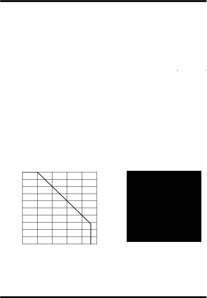
3.Performance Curves
3.1Derating Curves
|
|
100 |
|
|
|
|
|
(%) |
100 |
|
|
|
|
|
|
|
|
|
|
|
|
|
|
|
|
|
|
||
|
|
|
|
|
|
|
|
|
|
|
|
|
|
|
|
(%) |
80 |
|
|
|
|
|
Coefficient |
80 |
|
|
|
|
|
|
|
|
|
|
|
|
|
|
|
|
|
|||
|
|
|
|
|
|
|
|
|
|
|
|
|
||
Safe OperatingArea |
Temperature DeratingCoefficient |
60 |
|
|
|
|
|
Derating |
60 |
|
|
|
|
|
|
|
|
|
|
|
|
|
|
|
|
||||
|
|
|
|
|
|
|
|
|
|
|
|
|||
40 |
|
|
|
|
|
Temperature |
40 |
|
|
|
|
|
||
|
|
|
|
|
|
|
|
|
|
|
||||
20 |
|
|
|
|
|
20 |
|
|
|
|
|
|||
|
|
|
|
|
|
|
|
|
|
|
||||
|
|
|
|
|
|
AS |
|
|
|
|
|
|
||
|
|
|
|
|
|
E |
0 |
|
|
|
|
|
||
|
|
0 |
|
|
|
|
|
|
|
|
|
|
|
|
|
|
|
|
|
|
|
|
25 |
50 |
75 |
100 |
125 |
150 |
|
|
|
0 |
25 |
50 |
75 |
100 |
125 |
|
||||||
|
|
|
|
|
|
|
|
|
Channel Temperature, Tch (°C) |
Channel Temperature, Tch (°C) |
|
|
Figure 3-1 SOA Temperature Derating Coefficient Curve |
Figure 3-2 Avalanche Energy Derating Coefficient Curve |
STR-W6000S - DS Rev.2.0 |
SANKEN ELECTRIC CO.,LTD. |
5 |
Aug. 07, 2014 |
|
|
STR-W6000S Series
3.2Ambient Temperature versus Power Dissipation Curves
STR-W6051S |
|
|
|
|
|
STR-W6052S |
|
|
|
|
|
|||||||
|
30 |
|
|
|
|
|
|
|
|
30 |
|
|
|
|
|
|
|
R1 |
(W) |
25 |
PD1=22.3W |
|
|
|
|
STR-W6051S R1 |
(W) |
25 |
PD1=23.6W |
|
|
|
|
PD1 STR-W6052S |
|||
|
|
|
|
|
|
|
|
|
|
|
|
|
||||||
|
|
|
|
|
|
|
|
|
|
|
|
|
|
|
||||
D1 |
|
|
|
With infinite heatsink |
|
D1 |
|
|
|
|
|
With infinite heatsink |
||||||
Power Dissipation, P |
20 |
|
|
|
PD1 |
Power Dissipation, P |
20 |
|
|
|
|
|
|
|
|
|||
|
|
|
|
|
|
|
|
|
|
|
|
|
|
|||||
15 |
|
|
|
|
|
|
15 |
|
|
|
|
|
|
|
|
|||
10 |
|
|
|
|
|
|
10 |
|
|
|
|
|
|
|
|
|||
|
|
|
|
|
|
|
|
|
|
|
|
|
|
|
|
|||
|
5 |
|
|
Without heatsink |
|
|
|
|
5 |
|
|
Without heatsink |
|
|
|
|||
|
|
PD1=1.3W |
|
|
|
|
|
|
|
P |
D1 |
=1.3W |
|
|
|
|
|
|
|
0 |
|
|
|
|
|
|
|
|
0 |
|
|
|
|
|
|
|
|
|
|
0 |
25 |
50 |
75 |
100 |
125 |
150 |
|
0 |
|
|
25 |
50 |
75 |
100 |
125 |
150 |
|
|
|
Ambient Temperature, TA (°C ) |
|
|
|
|
|
|
Ambient Temperature, TA (°C ) |
|
|||||||
STR-W6053S |
|
|
|
|
|
STR-W6072S |
|
|
|
|
|
|||||||
|
30 |
|
|
|
|
|
|
PD1 STR-W6053S R1 |
|
30 |
|
|
|
|
|
|
|
PD1 STR-W6072S R1 |
|
|
|
|
|
|
|
|
|
|
|
|
|
|
|
|
|||
|
|
|
PD1=26.5W |
|
|
|
|
|
PD1=25.8W |
|
|
|
|
|||||
(W) |
25 |
|
|
With infinite heatsink |
|
(W) |
25 |
|
|
|
With infinite heatsink |
|
||||||
|
|
|
|
|
|
|
|
|||||||||||
|
|
|
|
|
|
|
|
|
|
|
|
|||||||
|
|
|
|
|
|
|
|
|
|
|
|
|
|
|
||||
D1 |
|
|
|
|
|
|
|
20 |
|
|
|
|
|
|
|
|||
P |
20 |
|
|
|
|
|
|
D1 |
|
|
|
|
|
|
|
|||
Power Dissipation, |
|
|
|
|
|
|
|
Power Dissipation, P |
|
|
|
|
|
|
|
|
|
|
15 |
|
|
|
|
|
|
|
15 |
|
|
|
|
|
|
|
|
||
|
|
|
|
|
|
|
|
|
|
|
|
|
|
|
|
|||
10 |
|
|
|
|
|
|
|
10 |
|
|
|
|
|
|
|
|
||
|
|
|
|
|
|
|
|
|
|
|
|
|
|
|
|
|||
5 |
|
|
Without heatsink |
|
|
|
5 |
|
|
|
Without heatsink |
|
|
|
||||
|
|
|
|
|
|
|
|
PD1=1.3W |
|
|
|
|
|
|||||
|
|
|
PD1=1.3W |
|
|
|
|
|
|
|
|
|
|
|
|
|||
|
|
|
|
|
|
|
|
|
|
|
|
|
|
|
|
|
|
|
|
0 |
|
|
|
|
|
|
|
|
0 |
|
|
|
|
|
|
|
|
|
|
|
|
|
|
|
|
|
0 |
|
|
25 |
50 |
75 |
100 |
125 |
150 |
|
|
|
0 |
25 |
50 |
75 |
100 |
125 |
150 |
|
|
|
|||||||
|
|
|
|
|
|
|
|
|
|
|
|
|||||||
|
|
|
Ambient Temperature, TA (°C ) |
|
|
|
|
|
|
Ambient Temperature, TA (°C ) |
|
|||||||
STR-W6000S - DS Rev.2.0 |
SANKEN ELECTRIC CO.,LTD. |
6 |
Aug. 07, 2014 |
|
|
STR-W6000S Series
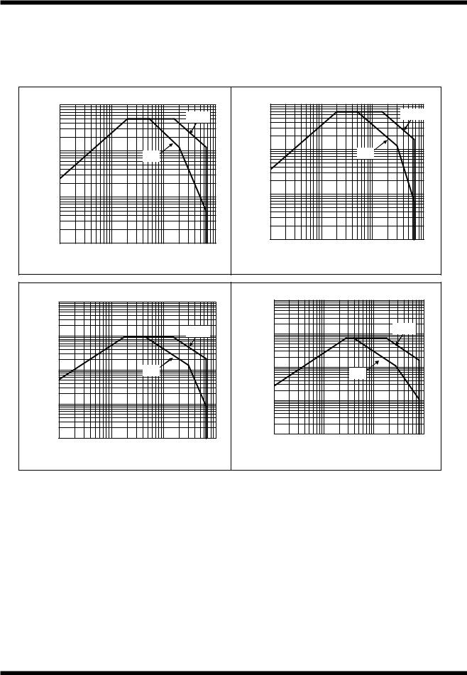
3.3MOSFET Safe Operating Area Curves
When the IC is used, the safe operating area curve should be multiplied by the temperature derating coefficient derived from Figure 3-1.
The broken line in the safe operating area curve is the drain current curve limited by on-resistance.
Unless otherwise specified, TA = 25 °C, Single pulse
Drain Current, ID (A)
STR-W6051S |
|
|
STR-W6052S |
|
|
|||
10 |
|
|
|
|
10 |
|
|
|
|
|
|
0.1ms |
|
|
|
|
0.1ms |
|
|
|
|
|
|
|
SOASTR-W6052SR1 |
|
|
|
|
SOASTRW6051SR1 |
I |
|
|
|
|
1 |
|
1ms |
|
(A) |
1 |
|
1ms |
|
|
|
|
D |
|
|
|
|
|
|
|
|
|
|
|
|
|
|
|
|
|
|
Current, |
0.1 |
|
|
|
0.1 |
|
|
|
Drain |
|
|
|
|
|
|
|
|
|
|
|
||
|
|
|
|
|
|
|
|
|
0.01 |
|
|
|
|
0.01 |
|
|
|
|
|
|
|
1 |
10 |
100 |
1000 |
|
1 |
10 |
100 |
1000 |
|
||||
|
|
|
|
|
||||
|
Drain-to-Source Voltage (V) |
|
|
|
Drain-to-Source Voltage (V) |
|
||
STR-W6053S |
|
|
|
STR-W6072S |
|
|
|
|
100 |
|
|
R1 |
100 |
|
|
|
|
|
0.1ms |
W6053S_ |
|
|
0.1ms |
|
|
|
STR- |
10 |
|
||
|
10 |
|
|
|
|||
|
|
|
|
|
|||
D |
|
|
(A) |
|
|
||
(A) |
|
|
|
SOA_ |
|
|
|
DrainCurrent, I |
|
|
|
D |
|
|
|
0.1 |
|
|
Current,Drain I |
|
|
||
|
1 |
|
1ms |
|
1 |
|
1ms |
|
|
|
|
|
|
|
|
|
|
|
|
|
0.1 |
|
|
|
0.01 |
|
|
|
0.01 |
|
|
|
|
|
|
1 |
10 |
100 |
|
|
1 |
10 |
100 |
1000 |
|||
|
|
|
|
||||
|
|
Drain-to-Source Voltage (V) |
|
|
Drain-to-Source Voltage (V) |
||
SOA_STR-W6072S_R1
1000
STR-W6000S - DS Rev.2.0 |
SANKEN ELECTRIC CO.,LTD. |
7 |
Aug. 07, 2014 |
|
|

STR-W6000S Series
3.4Transient Thermal Resistance Curves
STR-W6051S |
|
|
|
|
|
|
|
10 |
|
|
|
|
TR STR-W6051S R1 |
Transient Thermal Resistance θch-c (°C/W) |
1 |
|
|
|
|
|
0.1 |
|
|
|
|
||
0.01 |
10µ |
100µ |
1m |
10m |
||
|
1µ |
100m |
||||
Time (s)
STR-W6052S |
|
|
|
|
|
|||
|
|
10 |
|
|
|
|
|
TR STR-W6052S R1 |
Transient Thermal Resistance |
θch-c (°C/W) |
1 |
|
|
|
|
|
|
0.1 |
|
|
|
|
|
|||
0.01 |
|
|
|
|
|
|||
|
|
1µ |
10µ |
100µ |
1m |
10m |
100m |
|
Time (s)
STR-W6053S |
|
|
|
|
|
||
|
|
10 |
|
|
|
|
TR STR-W6053S R1 |
Transient Thermal Resistance |
|
1 |
|
|
|
|
|
θch-c (°C/W) |
0.1 |
|
|
|
|
||
0.01 |
|
|
|
|
|||
0.001 |
|
|
|
|
|||
|
|
1µ |
10µ |
100µ |
1m |
10m |
100m |
Time (s)
STR-W6072S |
|
|
|
|
|
||
Transient Thermal Resistance |
|
10 |
|
|
|
|
TR STR-W6072S R1 |
θch-c (°C/W) |
1 |
|
|
|
|
||
0.1 |
|
|
|
|
|||
0.01 |
|
|
|
|
|||
0.001 |
10µ |
100µ |
1m |
10m |
|||
|
|
1µ |
100m |
||||
Time (s)
STR-W6000S - DS Rev.2.0 |
SANKEN ELECTRIC CO.,LTD. |
8 |
Aug. 07, 2014 |
|
|
 Loading...