

Sep. 2 0 0 1 GT-6 (T)
SERVICE N OTES
First Edition
Guitar Effects Processor
TABLE OF CO N TEN TS
TABLE OF CONTENTS ...................................................1
SPECIFICATIONS.............................................................2
LOCATION OF CONTROLS PARTS LIST ...................4
LOCATION OF CONTROLS ..........................................4
EXPLODED VIEW PARTS LIST .....................................6
EXPLODED VIEW ............................................................6
WIRING DIAGRAM.........................................................8
PARTS LIST........................................................................9
IDENTIFYING THE VERSION NUMBER ..................14
TRANSMITTING / RECEIVING DATA
VIA MIDI..........................................................................14
BULK DUMP ...................................................................14
BULK LOAD....................................................................14
Issued by RJA
TEST MODE.....................................................................14
RESTORING THE FACTORY SETTINGS
(FACTORY RESET).........................................................19
HOW TO UPDATE SYSTEM SOFTWARE .................19
BLOCK DIAGRAM.........................................................21
CIRCUIT BOARD (MAIN) ............................................22
CIRCUIT BOARD (MAIN) ............................................24
CIRCUIT DIAGRAM (MAIN 1/2) ...............................26
CIRCUIT DIAGRAM (MAIN 2/2) ...............................28
CIRCUIT BOARD (SW SHEET) ....................................30
CIRCUIT DIAGRAM (SW SHEET) ..............................32
ERROR MESSAGE ..........................................................34
Copyright © 20 0 2 ROLAN D CORPORATIO N
All rights reserved. No part of this publication may be reproduced in any form without the written permission
of ROLAND CORPORATION.
Printed in Japa n (0 8 0 0) (CM)

Sep. 2 0 0 1
SPECIFICATIO N S
GT-6 : Guita r Effects Processor
• AD Conversion
24 bit + AF method
• DA Conversion
24 bit
• Sampling Frequency
44.1 kHz
• Program Memories
340: 140 (User) + 200 (Preset)
• Nominal Input Level
INPUT: -10 dBu
RETURN: -10 dBu
• Input Impedance
INPUT: 1 M ohms
RETURN: 220 k ohms
• Nominal Output Level
OUTPUT: 0 dBu
SEND: -10 dBu
• Output Impedance
OUTPUT: 2 k ohms
SEND: 2 k ohms
• Digital Output
EIAJ CP1201, S/P DIF
• Dynamic Range
100 dB or greater (IHF-A)
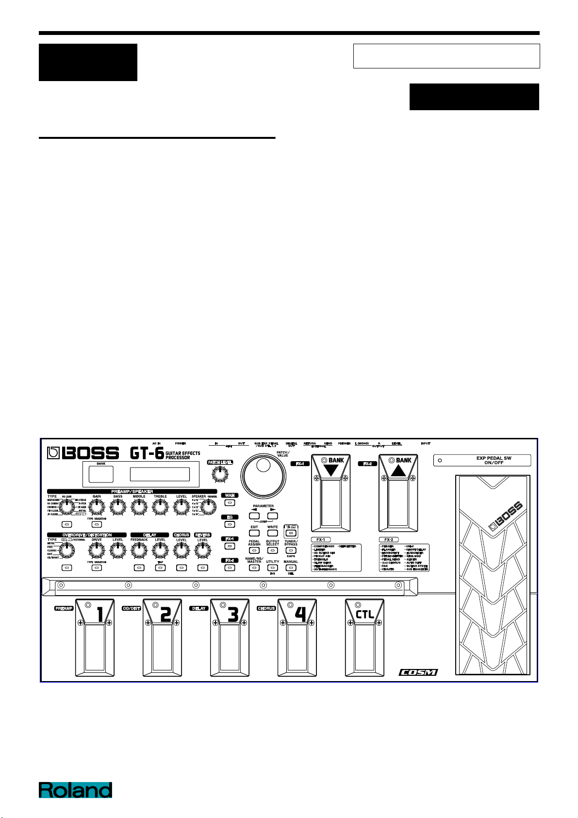
• Controls
< Front Panel >
(PREAMP/SPEAKER)
TYPE knob
GAIN knob
BASS knob
MIDDLE knob
TREBLE knob
LEVEL knob
SPEAKER knob
On/Off button
TYPE VARIATION button
(OVERDRIVE/DISTORTION)
TYPE knob
DRIVE knob
LEVEL knob
On/Off button
TYPE VARIATION button
(DELAY)
FEEDBACK knob
LEVEL knob
On/Off button
TAP button
(CHORUS)
LEVEL knob
On/Off button
(REVERB)
LEVEL knob
On/Off button
(WAH)
On/Off button
(EQ)
On/Off button
(FX-1)
On/Off button
(FX-2)
On/Off button
(MASTER)
PATCH LEVEL knob
PARAMETER buttons L/R
EXIT button
WRITE button
EZ TONE button
PEDAL ASSIGN button
OUTPUT SELECT button
TUNER/BYPASS button
NAME/NS/MASTER button
UTILITY button
MANUAL button
Number pedals1-4
BANK pedals (Up/Down)
CTL pedal
Expression pedal
Expression pedal switch
PATCH/VALUE dial
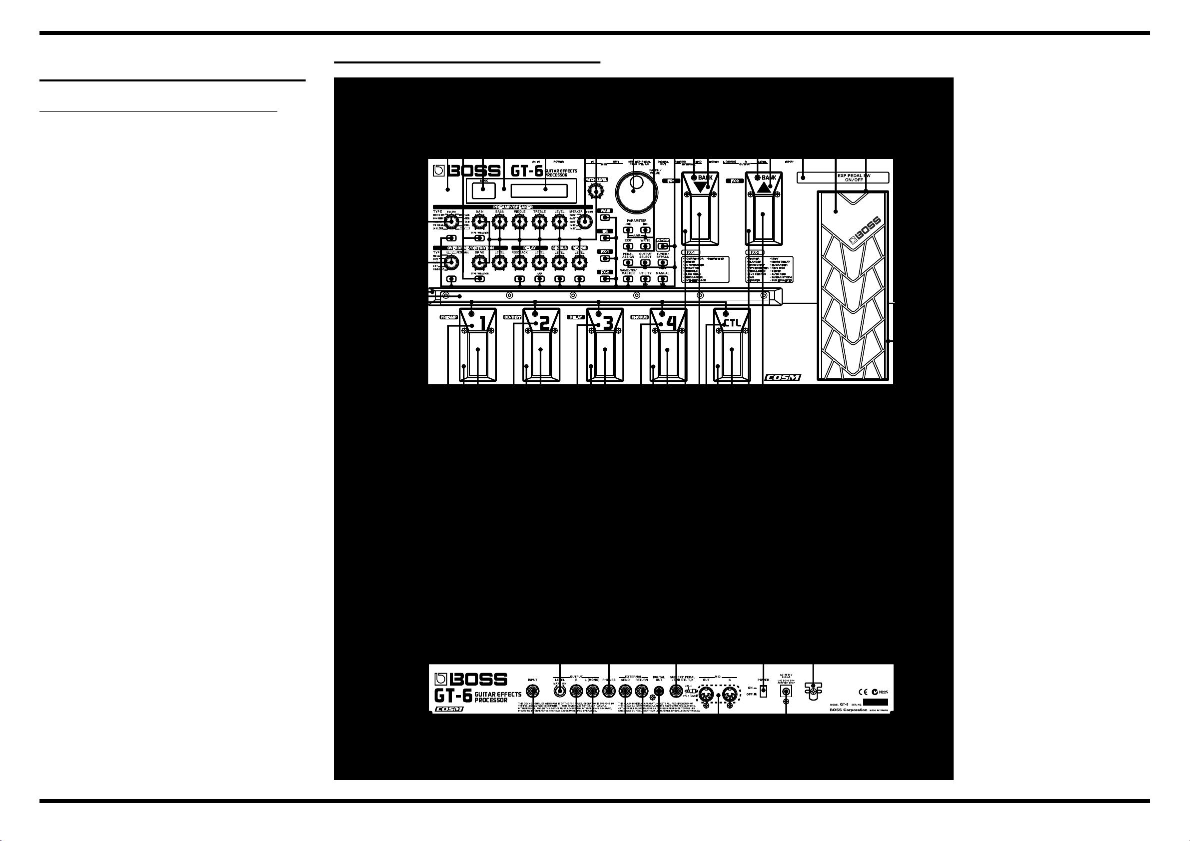
< Rear Panel >
OUTPUT LEVEL knob
POWER switch
Display
16 characters, 2 lines (backlit LCD)
2 characters, 7 segment LED
Connectors
INPUT jack
OUTPUT jacks L (MONO)/R
PHONES jack
SEND jack
RETURN jack
DIGITAL OUT connector (coaxial)
SUB EXP PEDAL/SUB CTL PEDAL1,2 jack
MIDI connectors IN/OUT
AC Adaptor jack
• Power Supply
AC 14 V; Supply AC adaptor (BOSS BRC series)
• Current Draw
800 mA
• Dimensions
515 (W) x 261 (D) x 75 (H) mm
20-5/16 (W) x 10-5/16 (D) x 3 (H) inches
• Weight
4.7 kg/10 lbs 6 oz (excluding AC Adaptor)
• Accessories
Owner’s Manual English (#G6017298)
AC Adaptor BRC-120V (#01786223)
AC Adaptor BRC-230V (#01786234)
AC Adaptor BRC-240V (#01786245)
EURO CONVERTER PLUG ECP01-5A (PLUG for 230V) (#00905234)
• Options
MIDI Implementation English (#17041119)
Foot Switch: FS-5U, FS-5L
Expression Pedal: EV-5 (Roland), FV-300L + PCS-33 (Roland)
Foot Switch Cable: PCS-31 (Roland)
(1/4 inches Phone Plug (stereo) - 1/4 inches Phone Plug (mono) x 2)
* 0 dBu = 0.775 Vrms
* In the interest of product improvement, the specifications and/or appearance of
this unit are subject to change without prior notice.
2

GT-6 (T)
3
54
Sep. 2 0 0 1 GT-6 (T)
LOCATIO N OF CON TROLS PARTS LIST
No. Part Code Part Name Q’ty
1 G2477122 R-KNOB 15
2 F3279803 POTENTIOMETER RD901-40-125F-
B54-11D (11 click)
3 F3279804 POTENTIOMETER RD901-40-125F-
B54-06D (6 click)
4 F3279802 POTENTIOMETER RD901-40-125F-
B54-00D
5 G2237113 GUARD PLATE 1
6 G2237112 GUARD 1
7 G2017152 TOP COVER 1
8 F5029412 LED (RED) A-552SR BW 1
9 F5029405 LMC-SSC2K16DLNY-H01 1
10 G2567119 DISPLAY COVER 1
11 22485303 D R-KNOB L BLK 248-303 1
12 01905467 ROTARY ENCODER EVE GC1 F20
24B
13 G2567118 ESCUTCEON (for PANEL) 1
14 G247751301 KEYTOP S WITHOUT LENS 4
15 G247751001 KEYTOP S BLACK WITH LENS 19
16 F5029111 LED (RED/GREEN) L-3WSRSGW-CC2
17 F5029117 LED (RED) L-312LRD 17
18 1502928100 LED (RED) L-34HDSL 8
19 01780101 TACT SWITCH SKQKAB 23
20 G2217138 PEDAL LABEL(1) 1
21 G2217139 PEDAL LABEL(2) 1
22 G2217140 PEDAL LABEL(3) 1
23 G2217143 PEDAL LABEL(4) 1
24 G2217144 PEDAL LABEL(CTL) 1
25 G2217142 PEDAL LABEL(DOWN) 1
26 G2217141 PEDAL LABEL(UP) 1
27 G2357112 VR PLATE 1
28 G2567121 RUBBER SW ESCUTCHEON 1
29 G2567120 RUBBER SW 1
30 G2187533 VR PEDAL 1
31 G2187904 PEDAL HOLDER 1
32 01016167 11M/M ROTARY POT.
RK11K1140(10K SP B)
33 G2357111 CUSHION R 1
34 G2147117 PIN STAY 1
35 G2147119 BOLT HOLDER 2
36 G2357120 FOOT H=5 5
37 G2147116 SHAFT STAY 1
38 G2227301 PEDAL ESCUTCHEON 7
39 G2187602 SWITCH PEDAL 7
40 G2177103 SUPPORT SPRING 7
41 G2357109 PEDAL FOOT 7
42 13129778 TACT SWITCH SKQKAH 7
43 G2017150 BOTTOM COVER 1
44 13449155MF PHONE JACK (MONO) HTJ-064-12I 5
45 13449150MF PHONE JACK (STEREO) HTJ-064-
12D
46 01340412 P R-KNOB SF-A BLK/LCG 1
47 01676523 9M/M ROTARY POT. RK09K12A0
10KAX2
48 01343723 RCA(PIN) JACK YKC21-3117 1
49 13429825 MIDI CONNECTOR YKF51-5054 1
50 12499175 G S-BUTTON S1H BLK 1
51 01676512 PUSH SWITCH SDKLA1-B 1
52 13449728 ADAPTOR JACK HEC0740-010010 1
53 22360712 CORD HOOK 236-712 1
LOCATIO N OF CON TROLS
fig.panel
14.19.
23.
15.17.19.
25. 26.
24.
50.51.
18.
53.
28.29.
27.
39.40.41.42
38.
30.31.32.33.
34.35.37.
1.2.
5.
15.16.19.
10.
1.3.
11.12.13.
1
2
12
1
1
1.3.
6.
18.
2
1
7.
20.
8.
21.
9.
46.47.
1.4.
22.
45.
36.43.
44.
48.
49.
52.

Sep. 2 0 0 1 GT-6 (T)
EXPLODED VIEW PARTS LIST
[Parts]
No. Part Code Part Name
1 G2017152 TOP COVER
2 G2017150 BOTTOM COVER
3 G2237112 GUARD
4 G2237113 GUARD PLATE
5 G2567120 RUBBER SW
6 G2567121 RUBBER SW ESCUTCHEON
7 G2357120 FOOT H=5
8 G2567119 DISPLAY COVER
9 12499175 G S-BUTTON S1H BLK
10 22485303 D R-KNOB L BLK
11 01340412 P R-KNOB SF-A BLK/LCG
12 22360712 CORD HOOK 236-712
13 G2217138 PEDAL LABEL(1)
14 G2217139 PEDAL LABEL(2)
15 G2217140 PEDAL LABEL(3)
16 G2217143 PEDAL LABEL(4)
17 G2217144 PEDAL LABEL(CTL)
18 G2217141 PEDAL LABEL(UP)
19 G2217142 PEDAL LABEL(DOWN)
20 G247751001 KEYTOP S BLACK WITH LENS
21 G247751301 KEYTOP S WITHOUT LENS
22 G2147116 SHAFT STAY
23 G2477122 R-KNOB
24 G2567118 ESCUTCEON (ABS,for PANEL)
25 G2227301 PEDAL ESCUTCHEON
26 G2187602 SWITCH PEDAL
27 G2177103 SUPPORT SPRING
28 G2357109 PEDAL FOOT
29 G2187904 PEDAL HOLDER
30 G2187533 VR PEDAL
31 G2357111 CUSHION R
32 G2147117 PIN STAY
33 G2357112 VR PLATE
34 F5029405 LCD
35 75D523S000 SW1 BOARD
36 75D523S000 SW2 BOARD
37 75D523S000 SW3 BOARD
38 75D523M000 MAIN BOARD
39 75D523S000 SW4 BOARD
40 75D523S000 SW5 BOARD
41 G2147119 BOLT HOLDER
42 12569249S0 LITHIUM BATTERY CR2032
EXPLODED VIEW
fig.jack
25
28
27
24
20
35
34
g
h
a
8
4
3
26
s
13
37
23
d
14
15
16
17
21
7
10
b
c
33
k
19
18
1
6
5
41
q
r
32
36
29
41
31
p
q
o
30
[Screws]
No. Part Code Part Name
a H5029854 HEX BUTTON BOLT M3x12 FeNi
b ******** M9 NUT (with ENCODER)
c H5039126 M9 WASHER (with ENCODER)
d H5039520 M9 NUT (VR)
e H5039510 NUT M9x11x2 FeNi (for Phone Jack)
f H5039112 WASHER M9 (for Phone Jack)
g 40342701 SCREW 2.3x8 BINDING TAPTITE P ZC
h 40011278 SCREW 3x8 BINDING TAPTITE P ZC
I 40011312 SCREW 3x8 BINDING TAPTITE P BZC
k 40127689 SCREW M3x10 BINDING TAPTITE S BZC
m H5019124 SCREW M3x6 BINDING W/PW+SW ZC
(Small Washer)
n H5019130 SCREW M3x6 BINDING W/PW+SW ZC
(Normal Washer)
o 40015901 E-RING M2.5 SUS
p 40342690 HEX BOLT M6x85 HALF THREAD BZC
q 40016067 PLAIN WASHER 6x13x1 BZC
r 40016001 NUT M6 U BZC
s 40019123 SCREW 3x8 BINDING TAPTITE S BZC
42
h
h
h
n
12
k
s
9
i
11
f
e
38
m
39
s
d
22
c
40
m
2
76
Sep. 2 0 0 1
W IRIN G DIAGRAM
SW2 BOARD ASSY
WIRING 10P
CN2
CN1
WIRING 8P
CN11
SW1
CN7
WIRING 11P
CN7
BOARD
CN3
WIRING 7P
CN8
ASSY
CN6
RIBON 3P
CN5
ENC BOARD
ASSY
CN6
MAIN BOARD ASSY
CN2
RIBON 7P
CN3
SW3 BOARD
ASSY
CN8
CN4
EXP BOARD
ASSY
CN4
SW4 BOARD
ASSY
CN10
WIRING 2P
WIRING 3P
8

PARTS LIST
fig.part1e
IC
GT-6 (T)
SAFETY PRECAUTIONS:
The parts marked have
safety-related characteristics. Use
only listed parts for replacement.
NOTE: The parts marked # are new. (initial parts)
fig.part2e
NOTE: Consider about the natural environment carefully before through the old lithium battery away when you exchange to the new one.
MB -> MAIN BOARD ASSY, SW -> SW SHEET ASSY
CASING Q'ty
# G2017150 BOTTOM COVER 1
# G2357120 FOOT H=5 5
# G2017152 TOP COVER 1
# G2187533 VR PEDAL 1
KNOB, BUTTON
G2227301 PEDAL ESCUTCHEON 7
G2357109 PEDAL FOOT 7
G2187602 SWITCH PEDAL 7
01340412
12499175 G S-BUTTON S1H BLK 249-175 1
22485303 D R-KNOB L BLK 248-303 for ALPHA-DIAL 1
G2477122 R-KNOB 15
G247751001 kEYTOP S BLACK WITH LENS for SW 19
G247751301 KEYTOP S WITHOUT LENS for SW 4
SAFETY PRECAUTIONS:
The parts marked have safety-related characteristics. Use only listed parts for replacement.
Failure to completely fill the above items with correct number and description will result in delayed or even
undelivered replacement.
P R-KNOB SF-A BLK/LCG 1
QTY PART NUMBER DESCRIPTION MODEL NUMBER
Ex. 10 22575241 Sharp Key C-20/50
15 2247017300 Knob (orange) DAC-15D
SWITCH
# G2567120 RUBBER SW 1
JACK, EXT TERMINAL
DISPLAY UNIT
# F5029405 LMC-SSC2K16DLNY-H01 LCD 1
# F5029412 A-552SR BW 7SEG LED LED29 on SW 1
PCB ASSY
# 75D523M000 MAIN BOARD ASSY 1
# 75D523S000 SW SHEET ASSY 1
# 02676190 HD6412312VF IC (CPU) IC21 on MB 1
# 02672378 UPD431000AGW-A10 IC (SRAM) IC22 on MB 1
01676512 SDKLA1-B PUSH SWITCH SW1 on MB 1
01780101 SKQKAB TACT SWITCH SW9,SW10,SW11,SW12,SW13,SW14,SW15,
13129778 SKQKAH TACT SWITCH SW1,SW2,SW3,SW4,SW5,SW6,SW7 on SW 7
13449155MF HTJ-064-12I PHONE JACK (MONO) JK1,JK3,JK4,JK5,JK6 on MB 5
13449150MF HTJ-064-12D PHONE JACK (STEREO) JK2,JK11 on MB 2
01343723 YKC21-3117(ORANGE) RCA(PIN) JACK JK9 on MB 1
13429825 YKF51-5054 2PZ MIDI CONNECTOR JK8 on MB 1
13449728 HEC0740-010010 ADAPTOR JACK JK7 on MB 1
02231767 RA0A-101 (TC223C080AF-101) IC (DSP) IC20 on MB 1
02451434 AK4552VT IC (AD/DA) IC3,IC8 on MB 2
******** LH28F400BVE-BL85 IC (FLASH MEMORY/
BLANK)
01785178 TC9271FS IC (DIF/TRANS MITTER) IC19 on MB 1
02453389 LC32V4265T-25 IC (DRAM) IC24 on MB 1
15289109 M5216FP-600D IC (BIPOLAR OP AMP) IC5 on MB 1
15189261 M5218AFP-600E IC (BIPOLAR OP AMP) IC6,IC4 on MB 2
00346445 NJM2100M(TE3) IC (BIPOLAR OP AMP) IC7,IC2 on MB 2
15259769T0 TC74HC238AF(EL) IC (CMOS) IC29 on MB 1
15169596 TC74HC4051AP IC (CMOS) IC4,IC5 on SW 2
01901623 TC74LVXC3245FS IC (CMOS) IC14 on MB 1
SW16,SW17,SW18,SW19,SW20,SW21,SW22
,SW23,SW24,SW25,SW26,SW27,SW28,SW2
9,SW30,SW31 on SW
IC26 on MB 1
23
9

Sep. 2 0 0 1
IC
# 02678945 BU2090 IC (LED DRIVER) IC2,IC3,IC6 on SW 3
# 02786678 S-81233SGY IC (REGULATOR) IC31 on MB 1
TRANSISTOR
# F5309115 2SA1241-Y TRANSISTOR Q12 on MB 1
# F5309601 2SB1132 TRANSISTOR Q14 on MB 1
# F5309602 2SB1182 TRANSISTOR Q8 on MB 1
# F5319601 2SD1664 TRANSISTOR Q13 on MB 1
# F5319602 2SD1758 TRANSISTOR Q7 on MB 1
DIODE
01670745 TC74VHCT541AF IC (CMOS) IC18 on MB 1
02232834 TC7SH04F(TE85L) IC (CMOS) IC27,IC17 on MB 2
15249121 TC7W04F(TE12L) IC (CMOS) IC16 on MB 1
02340756 TC7WH32FU(TE12L) IC (CMOS) IC28 on MB 1
00458034 TC75S51F TE85R IC (OP AMP) IC25 on MB 1
15289106 M5238AFP-600C IC (JFET OP AMP) IC1 on MB 1
02453056 BU2090F-E2 IC (LED DRIVER) IC1 on SW 1
15289124 PC-400 IC (PHOTO COUPLER) IC13 on MB 1
02012789 BA17805FP-E2 IC (REGULATOR) IC10 on MB 1
02563467 NJM2374AM-TE1 IC (SWITCHING REGULA-
TOR)
15289123 M51953AFP-600C IC (RESET) IC15 on MB 1
15309104 2SA1586-GR(TE85R) TRANSISTOR Q5,Q15 on MB 2
15319107 2SC4116-GR(TE85R) TRANSISTOR Q9 on MB 1
15329501 DTA143EKA T146 DIGITAL TRANSISTOR Q11 on MB 1
02340645 RN1441-A(TE85L) DIGITAL TRANSISTOR Q1,Q2,Q3,Q4,Q6 on MB 5
15129215 RN2207-TPE4 DIGITAL TRANSISTOR Q1,Q2,Q3,Q4 on SW 4
15019126 1SS133 T-77 SWITCHING DIODE D1,D2,D3,D4,D5,D6,D7,D9,D10,D11,D12,D
15339119T0 1SS352(TPH3) SWITCHING DIODE D1,D6,D8,D10,D11,D16,D17 on MB 7
F5019209RT 1N4004 DIODE D2,D4,D5,D12 on MB 4
02783023 RB500V-40 DIODE D9 on MB 1
F5339137 SS14 VF=0.45V DIODE D3 on MB 1
F5339310 RD10ESAB2 ZENER DIODE D13,D14 on MB 2
F5029117 L-312LRD LED (RED) LED9,LED10,LED11,LED12,LED13,LED14,
1502928100 L-34HDSL LED (RED) LED1,LED2,LED3,LED4,LED5,LED6,LED7,
F5029111 L-3WSRSGW-CC LED (RED/GREEN) LED27,LED28 on SW 2
15339120T0 1SS302(TE85R) DIODE ARRAY DA3,DA4 on MB 2
IC9 on MB 1
13,D14,D15,D16,D17,D18,D19,D20,D21,D22
,D23,D24,D25,D26,D27,D28,D29,D30,D31on
SW
LED15,LED16,LED17,LED18,LED19,LED20
,LED21,LED22,LED23,LED24,LED25 on SW
LED8 on SW
30
17
8
RESISTOR
F3829254 47 OHM(2W) CARBON RESISTOR R11,R14 on MB 2
13749775T0 SR25TRE 121 J CARBON RESISTOR R23,R21 on SW 2
13749789T0 SR25TRE 471 J CARBON RESISTOR R31,R32,R33,R34,R35,R36,R37,R38,R39,R40,
R41,R42,R43,R44 on SW
00566867 RPC05T 100 J MTL.FILM RESISTOR R9,R54,R109 on MB 3
00567023 RPC05T 101 J MTL.FILM RESISTOR R69,R108 on MB 2
00567156 RPC05T 102 J MTL.FILM RESISTOR R21,R22,R32,R33,R55,R56,R100,R104,R107,
R113 on MB
00567289 RPC05T 103 J MTL.FILM RESISTOR R2,R6,R12,R13,R16,R19,R24,R27,R30,R35,R
37,R38,R41,R45,R47,R48,R52,R61,R72,R76,R
80,R82,R102,R105,R119,R120,R130,R132,R13
3,R134,R137 on MB
00567412 RPC05T 104 J MTL.FILM RESISTOR R23,R34,R58,R59,R116 on MB 5
00567556 RPC05T 105 J MTL.FILM RESISTOR R39,R7 on MB 2
00567034 RPC05T 121 J MTL.FILM RESISTOR R67 on MB 1
00567167 RPC05T 122 J MTL.FILM RESISTOR R40,R1 on MB 2
00567178 RPC05T 152 J MTL.FILM RESISTOR R65,R142 on MB 2
00567189 RPC05T 182 J MTL.FILM RESISTOR R66 on MB 1
00567312 RPC05T 183 J MTL.FILM RESISTOR R42,R3 on MB 2
00566912 RPC05T 220 J MTL.FILM RESISTOR R77 on MB 1
00567190 RPC05T 222 J MTL.FILM RESISTOR R112,R68 on MB 2
00567456 RPC05T 224 J MTL.FILM RESISTOR R46 on MB 1
00567089 RPC05T 331 J MTL.FILM RESISTOR R25,R36,R74 on MB 3
00567345 RPC05T 333 J MTL.FILM RESISTOR R51,R57 on MB 2
00567112 RPC05T 471 J MTL.FILM RESISTOR R70 on MB 1
00567245 RPC05T 472 J MTL.FILM RESISTOR R85,R91,R94,R103,R106,R110,R111,R114,R1
15 on MB
00567378 RPC05T 473 J MTL.FILM RESISTOR R17,R20,R28,R31,R49,R60,R122,R123,R124
on MB
00567501 RPC05T 474 J MTL.FILM RESISTOR R84 on MB 1
00567001 RPC05T 750 J MTL.FILM RESISTOR R71 on MB 1
00567401 RPC05T 823 J MTL.FILM RESISTOR R26,R15 on MB 2
15399349 RPC10T 100 J 1/10W MTL.FILM RESISTOR R139,R140,R141 on MB 3
01905012 RR0816P-123-D MTL.FILM RESISTOR R4,R8,R43,R50 on MB 4
14
10
31
9
9
1 0

GT-6 (T)
RESISTOR
# F5399911 0.68 (1/2W) RESISTOR R62 on MB 1
# F5399912 1.8K (F-RANK) RESISTOR R64 on MB 1
# F5399919 1M(F-RANK) RESISTOR R81 on MB 1
# F5399917 22 (1/2W) RESISTOR R75 on MB 1
# F5399913 3K (F-RANK) RESISTOR R63 on MB 1
# F5399920 4.7M(F-RANK) RESISTOR R121 on MB 1
# 13749787T0 SR25TRE 391J 1/6W RESISTOR R1,R2,R3,R4,R5,R6,R7,R8,R9,R10,R11,R12,R
POTENTIOMETER
CAPACITOR
# 13639582S0 35MV100HW+T CHEMICAL CAPACITOR C64,C67,C70,C74 on MB 4
# 13639598 35MV220HW+T CHEMICAL CAPACITOR C144 on MB 1
# 13609111 50MVR33HW+T CHEMICAL CAPACITOR C90 on MB 1
01909734 RR0816P-682-D MTL.FILM RESISTOR R10,R53 on MB 2
02122623 RR0816R-104-D MTL.FILM RESISTOR R5,R44 on MB 2
13,R14,R15,R16,R17,R18,R19,R20,R22,R24,R
F5419707 CRN34101J RESISTOR ARRAY RA1,RA2,RA4,RA6,RA12,RA15 on MB 6
F5419705 CRN34103J RESISTOR ARRAY RA11,RA14,RA18,RA19,RA28 on MB 5
F5419706 CRN34104J RESISTOR ARRAY RA5,RA3 on MB 2
F3279802 RD901-40-125F-B54-00D 50KB 9M/M ROTARY POT. W/
CLICK
F3279804 RD901-40-125F-B54-06D 50KB 9M/M ROTARY POT. 6
CLICKS
F3279803 RD901-40-125F-B54-11D 50KB 9M/M ROTARY POT. 11
CLICKS
01676523 RK09K12A0 10KAx2 9M/M ROTARY POT. VR1 on MB 1
01016167 RK11K1140(10K SP B) 10Kx1 11M/M ROTARY POT. VR1 on SW 1
01674167 ECJ1VC1H100D CERAMIC CAPACITOR C3,C6,C16,C25,C38,C41,C42,C145,C146,C15
01674701 ECJ1VF1E104Z 0.1UF/16VK CERAMIC CAPACITOR C7,C9,C12,C14,C44,C48,C50,C53,C58,C59,C
01674356 ECUV1H151JCV CERAMIC CAPACITOR C23,C33,C62 on MB 3
00567823 GRM39B102K50PT CERAMIC CAPACITOR C15,C24,C43,C54,C127 on MB 5
00567945 GRM39B103K50PT CERAMIC CAPACITOR C1,C36,C129,C130 on MB 4
01672412 GRM39CH150J50PT CERAMIC CAPACITOR C121,C119 on MB 2
13639550S0 16MV100HW+T 100UF/16V CHEMICAL CAPACITOR C21,C31,C66,C68,C69,C72,C157 on MB 7
13639546S0 16MV10HW+T CHEMICAL CAPACITOR C4,C8,C10,C11,C17,C18,C19,C20,C26,C27,C
13639549S0 16MV47HW+T CHEMICAL CAPACITOR C13,C45,C76,C81 on MB 4
13639195S0 35MV2200HW(SME35VB2200) CHEMICAL CAPACITOR C56 on MB 1
13639599S0 35MV470HW+T CHEMICAL CAPACITOR C65,C71 on MB 2
13639113S0 6MV470HW CHEMICAL CAPACITOR C61,C35 on MB 2
13519694 RPE132-901F104Z50 MLT.LAY.CERAMIC CAPACI-
TOR
13549279M0 ECQ-M1H104JF3 POLYEST. CAPACITOR C5 on MB 1
01128045 ERZVA7V330 VARISTOR CAPACITOR C55 on MB 1
25,R26,R27,R28,R29 on SW
VR2,VR4,VR6,VR7,VR8,VR9,VR10,VR11,V
R12,VR13,VR15,VR16 on SW
VR3,VR14 on SW 2
VR5 on SW 1
4 on MB
77,C78,C79,C80,C83,C84,C86,C87,C88,C89,
C91,C92,C93,C95,C96,C98,C99,C100,C101,C
102,C103,C105,C106,C107,C108,C109,C110,
C111,C112,C114,C115,C118,C120,C123,C12
4,C125,C128,C131,C132,C134,C135,C136,C1
38,C139,C140,C141,C142,C147,C148,C149,C
159,C160,C162,C163 on MB
28,C29,C30,C34,C39,C40,C46,C47,C49,C51,
C52,C94,C97,C104,C113,C116,C122,C126,C
133,C143,C150,C151,C152,C153 on MB
C1,C2,C3,C4,C5 on SW 5
27
12
10
64
34
INDUCTOR, COIL, FILTER
13529246 DSS310-91D223S-50ATL12-134 EMI FILTER FL1,FL2 on MB 2
12449386 SBT-0180W EMI FILTER L15 on MB 1
# F2449220 TSL1112SRA-471KR72 INDUCTOR L11 on MB 1
CRYSTAL, RESONATOR
# 02672401 SG-8002JC 67.7376MHZ PC CRYSTAL X1 on MB 1
00894023 MA-406 20.000MHZ TE24 CRYSTAL X2 on MB 1
ENCODER
01905467 EVE GC1 F20 24B ROTARY ENCODER EN1 on SW 1
CONNECTOR
# F3439160 53015-0210 CONNECTOR CN8 on MB 1
F3439166 A2001WR2-11P CONNECTOR CN3 on MB 1
# F3439179 A2001WR2-7P CONNECTOR CN6 on MB 1
F3439164 A2001WR2-8P CONNECTOR CN7 on MB 1
F3439165 A2001WV2-10P P=2MM CONNECTOR CN2 on MB 1
# F3439178 A2541WV2-2A16NP CONNECTOR 1
1 1

Sep. 2 0 0 1
CONNECTOR
WIRING, CABLE
#
# G3477156 7P P=2MM L=140MM RIBBON CABLE CN1,CN3 on SW 1
# G3467179 10P P=2MM L=120MM WIRING CN2 on SW 1
# G3467177 11P P=2MM L=65MM WIRING CN7 on SW 1
# G3467174 2P P=2MM L=150MM WIRING CN10 on SW 1
# G3467175 3P P=2MM L=115MM WIRING CN4 on SW 1
# G3467176 7P P=2MM L=115MM WIRING CN8 on SW 1
# G3467178 8P P=2MM L=65MM WIRING CN11 on SW 1
TRANSFORMER
SCREWS
# H5019130 SCREW M3x6 PAN MACHINE W/SW+PW
# H5029854 BOLT M3x12 HEX BUTTON FENI 6
# ******** M9 NUT (for ENCODER) 1
# H5039520 M9 NUT (for VR) 15
# H5039510 NUT M9x12x2 FENI (for Phone Jack) 7
# H5039126 M9 WASHER (for ENCODER) 1
# H5039112 M9 WASHER (for Phone Jack) 7
F3439121 A2541WR2-2A16NP CONNECTOR 16P CN1 on MB 1
F3439123 A2001WR2-3P CONNECTOR 3P CN4 on MB 1
G3467180 16P L=160MM LCD WIRING 1
G3477146 3P L=40X5X5 MM P=2MM RIBBON CABLE CN5,CN6 on SW 1
02563501 PT-10 (2280-T008) PULSE TRANS TR1 on MB 1
40342701 SCREW M2.3x8 BINDING TAP TIGHT P ZC 1
H5019124 SCREW M3x6 PAN MACHINE W/
40011312 SCREW 3x8 BINDING TAPTITE P BZC 3
40011278 SCREW 3x8 BINDING TAPTITE P FE ZC 20
40019123 SCREW 3x8 BINDING TAPTITE S BZC 18
40127689 SCREW M3x10 BINDING TAPTIGHT S TYPE
40342690 HEX BOLT M6x85 HALF THREAD BZC 1
40016001 LOCK NUT M6 U BZC 1
40015901 E-RING M2.5 SUS 1
40016067 PLAIN WASHER 6x13x1 BZC 2
ZC
SW+SMALL PW ZC
FE BZC
5
10
3
PACKING
# G2607214 PACKING CASE 1
# G2237620 PAD L 1
# G2237616 PAD R 1
# G2617273 OUTER PACKING CASE 1
MISCELLANEOUS
G2147118 AC JACK HOLDER on MB 1
G2147119 BOLT HOLDER 2
# G2607215 COLOR SLEEVE 1
22360712 CORD HOOK 236-712 1
G2357111 CUSHION R 1
# G2567119 DISPLAY COVER 1
# G2567118 ESCUTCHEON (ABS,for PANEL) 1
# G2237112 GUARD 1
# G2237113 GUARD PLATE 1
40016523 INSULOK TIE 100M/M T-18R <<1000 PCS ORDERING
PER>>
G2257203 JACK COVER on MB 1
# H2369431 LED SPACER 3-2 for SW 1
12569249S0 LITHIUM BATTERY CR2032 220MAH/3V BT1 for MB 1
12189815 LITHIUM BATTERY HOLDER BH-32 BT1 on MB 1
# G2187904 PEDAL HOLDER 1
# G2217138 PEDAL LABEL(1) 1
# G2217139 PEDAL LABEL(2) 1
# G2217140 PEDAL LABEL(3) 1
# G2217143 PEDAL LABEL(4) 1
# G2217144 PEDAL LABEL(CTL) 1
# G2217142 PEDAL LABEL(DOWN) 1
# G2217141 PEDAL LABEL(UP) 1
G2147117 PIN STAY 1
# G2567121 RUBBER SW ESCUTCHEON 1
G2147116 SHAFT STAY 1
H2369401 SPACER 3X6X10 for SW 7
G2177103 SUPPORT SPRING 7
G2357112 VR PLATE 1
2
1 2

ACCESSORIES (STANDARD)
# G6017297 OWNER’S MANUAL JAPANESE 1
# G6017298 OWNER’S MANUAL ENGLISH 1
01786212 AC ADAPTOR BRC-100T 1
01786223 AC ADAPTOR BRC-120T 1
01786234 AC ADAPTOR BRC-230T 1
01786245 AC ADAPTOR BRC-240AT 1
00905234 EURO CONVERTER PLUG ECP01-5A (PLUG for 230V) 1
# H5279511 READ ME FIRST JAPANESE/ENGLISH 1
40232389 WARRANTY CARD (JAPAN ONLY) 1
GT-6 (T)
1 3

Sep. 2 0 0 1
IDEN TIFYIN G THE VERSION N UM BER
1 . Turn the power off.
2 . While pressing [NAME/NS/MASTER],[UTILITY] and [MANUAL]
button, turn on power.
3 . The version number is displayed.
fig.LCD1
TRAN SMITTIN G / RECEIVIN G DATA VIA M IDI
The GT-6 can use exclusive messages to set another GT-6 to the same settings,
or to transmit its settings to a device such as a sequencer for storage.
The process of transmitting such data is called bulk dump, and the process of
receiving such data is called bulk load.
BULK DUM P
1 . Press [UTILITY] button, then press PARAMETER [<] [>] button so that
“Bulk Dump” is displayed.
fig.Dump-1
2 . Press PARAMETER [<] [>] button to move the cursor, and rotate the
[PATCH/VALUE] dial to select the start and end of the data to be
transmitted.
3 . When the data to be sent has been determined, press [WRITE] button.
The data is transmitted.
fig.Dump-2
When the transmission is completed, the screen prior to transmission
returns to the display.
4 . Press [EXIT] button to return to the Play screen.
BULK LO AD
1 . Press [UTILITY] button, then press PARAMETER [<] [>] button so that
“Bulk Load” is displayed.
fig.Load-1
fig.Load-3
•
•
At this stage, even more data can be received.
3 . Press [EXIT] button to quit Bulk Load.
After you press [EXIT] button, “Checking...” appears in the display,
indicating that the GT-6 is checking the received data.
When the check is completed, the Play screen returns to the display.
TEST M O DE
* Note: When user data is present, always back it up on the sequencer (MC-80,
etc.) before repair.
(Refer to “Saving data” and “Loading data” for the user data storage
procedures).
Individua l inspection items
1.DSP Check
2.Display
3.LCD Contrast
4.Switch
5.VR Check
6.EXP PEDAL
7.Battery
8.MIDI IN/OUT
9.OUTPUT D/A
10.EXT OD/DS
11.INPUT A/D
12.DSP INTO
13.Noise (IN -> OUT)
14.Noise (EXT)
15.Calibrete EXP
16.Factory Load
Required items
• Expression Pedal (Roland EV-5)
• MIDI Cable
• Noise Meter
• Oscilloscope
• Oscillator
• Equipment with digital input
• Empty plug
How to enter test mode:
Starting from “1.DSP Check”.
Turn on the unit while pressing the [DELAY] and [DELAY TAP] buttons
simultaneously.
The ROM version and the checksum will be displayed first.
Proceed to “1.DSP Check” by pressing the [EXIT] button.
fig.LCD1
2 . Transmit the data from the external MIDI device.
The following appears in the display when the GT-6 receives the data.
fig.Load-2
The following appears in the display when the GT-6 finishes receiving
the data.
1 4
Starting from “9.OUTPUT D/A”.
Turn on the unit while pressing the [CHORUS] and [REVERB] buttons
simultaneously.
“1.DSP Check” result is displayed first, then it proceeds to “9.OUTPUT
D/A”.

GT-6 (T)
1 . DSP Check
fig.LCD2
DSP (IC20) and DRAM (IC24) are automatically checked and their results
displayed.
If an error occurs, its contents will be displayed, and if no problems exist,
“OK” is displayed.
After the inspection completes, it will automatically proceed to the next
inspection.
2 . Display
fig.LCD3
All of the LCD and LED segments will be on.
Press the [EXIT] button to proceed to the next inspection.
3 . LCD Contrast
fig.LCD4
Turn the [VALUE] encoder knob in the following order and confirm that the
LCD contrast changes.
1) Turning the knob anti-clockwise dims the contrast.
fig.LCD5
2) Turning the knob clockwise brightens the contrast.
fig.LCD4
[2] The pedal switch group and expression switch inspection
[BANK DOWN] -> [BANK UP] -> [EXP PEDAL SW] -> [CTL PEDAL] ->
[PEDAL 4] -> [PEDAL 3] -> [PEDAL 2] -> [PEDAL 1]
[3] 7 seg LED
Confirm that the 7 seg LED segments go out one by one each time
[WAH] is pressed.
Pressing the [WAH] switch 14 times turns all the segments off .
After the [3] 7seg LED inspection completes, it will automatically proceed to
the next inspection.
5 . VR Check
fig.LCD7
Turn all the VRs anti-clockwise all the way (set to MIN position).
The names of the VRs to be inspected are displayed on the lower part of the
LCD.
Turn the displayed VR.
[PATCH LEVEL]->[SPEAKER]->[PRE LEVEL]->[PRE TREBLE]->[PRE
MIDDLE]->[PRE BASS]->[PRE GAIN]->[PRE TYPE]->[OD/DS TYPE]->[OD/
DS DRIVE]->[OD/DS LEVEL]->[DELAY FEEDBACK]->[DELAY LEVEL]>[CHORUS]->[REVERB]
1) Without click - the 7 seg LED segments come on from the bottom according
to the positions of the VR knobs, except for the “SPEAKER”, “PREAMP/
SPEAKER TYPE” and “OVERDRIVE/DISTORTION TYPE” VRs.
To proceed to the next VR inspection, turn the knob all the way to the right (
[MIN] -> [MAX] ).
2) With click - the numbers are displayed for the 7 seg LED segments
according to the clicked position, except for the “SPEAKER”, “PREAMP/
SPEAKER TYPE” and “OVERDRIVE/DISTORTION TYPE” VRs.
Change the LCD contrast from ‘15 -> 0 -> 15’, and it will automatically proceed
to the next inspection.
4 . Switch
fig.LCD6
The button names to be inspected are displayed on the lower part of the LCD.
Press the displayed button switches.
“Wrong switch!” is displayed when a wrong button is pressed.
Also, for buttons with LEDs confirm that:
1) All the LEDs that are on are red prior to pressing them.
2) The LEDs go out after the buttons are pressed.
However, for [PREAMP/SPEAKER TYPE VARIATION] and [OD/DS
TYPE VARIATION], the color changes from red to green.
Confirm the following two points.
Press the switches in the following order.
[1] Effect select button/Edit button group inspection Press according to the
LCD display.
[PREAMP/SPEAKER] -> [PREAMP/SPEAKER TYPE VARIATION]->[OD/
DS] -> [OD/DS TYPE VARIATION] -> [DELAY] -> [DELAY TAP] >[CHORUS] -> [REVERB] -> [FX-2] -> [FX-1] -> [EQ] -> [WAH] ->
[PARAMETER (<)] -> [EXIT] -> [PEDAL ASSIGN] -> [NAME/NS/MASTER] > [UTILITY] -> [OUTPUT SELECT] -> [WRITE] -> [PARAMETER (<)] -> [EZ
TONE] -> [TUNER/BYPASS] -> [MANUAL]
“SPEAKER” : [1x10] -> [ORIGINAL]
“PREAMP/SPEAKER TYPE” : [JC CLEAN] -> [CUSTOM]
“OVERDRIVE/DISTORTION TYPE” : [OD/BOOST] -> [CUSTOM/
EXTERNAL]
To proceed to the next VR inspection, turn the knob all the way to the right (
[MIN] -> [MAX] ).
After the [REVERB LEVEL] VR inspection completes, it will automatically
proceed to the next inspection.
6 . EXP PEDAL
fig.LCD8
Confirm the changes on the EXP pedal of this unit and the EXP pedal (SUB
EXP PEDAL) connected to the [SUB EXP PEDAL/SUB CTL 1,2] jack.
Connect the EV-5 to the [SUB EXP PEDAL/SUB CTL 1,2] jack.
The EXP pedal of this unit is inspected first, then the SUB EXP PEDAL.
1) Bringing the pedal’s tilt to the center (middle value) will display “***” in the
center display.
fig.LCD9
or
1 5

Sep. 2 0 0 1
fig.LCD13
2) Pressing further (maximum value) displays “***” on the right display.
fig.LCD10
or
fig.LCD14
3) Finally, returning the pedal forward (minimum value) displays “***” on the
left display, and the inspection for that pedal is complete.
fig.LCD11
or
fig.LCD15
Confirm these three points.
A) Using an oscilloscope, observe that a short wave is obtained from OUTPUT
.
B) Since output mute is automatically made ‘On/Off’, make sure that it is on.
C) Confirm that the level changes when the OUTPUT knob is turned.
fig.LCD20
Oscilloscope : 1.0 V/DIV, 0.5 ms/DIV
Mute = Off Mute = On
fig.1
After the EXP PEDAL inspection completes, it will automatically proceed to
the next inspection.
7 . Battery
fig.LCD16
The voltage of the memory backup battery is displayed.
To proceed to the next inspection, press the [EXIT] button.
8 . MIDI IN/OUT
fig.LCD18
Connect the MIDI IN connector and the MIDI OUT connector with a MIDI
cable.
“No Connect” is displayed if the connectors are not connected with a MIDI
cable.
If the connectors are properly connected, “Verify OK !” is displayed.
After the MIDI IN/OUT inspection completes, it will automatically proceed to
the next inspection.
fig.LCD17
fig.2
D) Confirm that a same waveform as that from OUTPUT is obtained from
Phones.
E) Confirm that a short wave is obtained from Send and that mute is effective.
Oscilloscope : 1.0 V/DIV, 0.5 ms/DIV
Mute = Off Mute = On
9 . OUTPUT D/A
Note : Check both L(MONO) and R.
Also, when the OUTPUT jack is used for a single channel, the L and R
signals will be internally mixed, therefore, empty plugs must be inserted
in the R channel for L(MONO) channel measurement and in the
L(MONO) channel for R channel measurement, respectively.
fig.LCD19
1 6

fig.3
fig.4
GT-6 (T)
fig.10ext-2e
DSP D/A SEND
(Signal source)
(Cut off)
DSP A/D RETURN
D/A OUTPUT
(Rectangular waveform)
Note: Check both L(MONO) and R.
Also, when the OUTPUT jack is used for a single channel, the L and R signals
will be internally mixed, therefore, empty plugs must be inserted in the R
channel for L(MONO) channel measurement and in the L(MONO) channel for
R channel measurement, respectively.
OUTPUT Level Control : MAX
Oscilloscope : 1.0 V/DIV, 0.5 ms/DIV
Insert an empty plug in RETURN
To proceed to the next inspection, press the buttons in [EXIT] ->
[PARAMETER (>)] sequence.
1 0 . EXT OD/DS
fig.LCD21
Confirm the following two points.
A) Using an oscilloscope, observe that a short wave is obtained from OUTPUT.
fig.10ext-1e
DSP D/A SEND
(Signal source)
fig.4
fig.2
DSP A/D RETURN
D/A OUTPUT
(Rectangular waveform)
B) Insert an open plug in the RETURN jack and confirm that there is no output.
To proeed to the next inspection, press the [EXIT] button.
1 7

Sep. 2 0 0 1
1 1 . INPUT A/D
fig.LCD22
Input a short wave, and observe the output waveform using an oscilloscope.
Note: Check both L(MONO) and R.
Also, when the OUTPUT jack is used for a single channel, the L and R signals
will be internally mixed, therefore, empty plugs must be inserted in the R
channel for L(MONO) channel measurement and in the L(MONO) channel for
R channel measurement, respectively.
INPUT : Rectangular Waveform, 400 Hz, 40 mVp-p
OUTPUT Level Control : MAX
Oscilloscope : 1.0 V/DIV, 0.5 ms/DIV
fig.5
fig.13noise-e
DSP A/D INPUT
D/A OUTPUT
(Connect noise meter)
To proceed to the next inspection, press the [EXIT] button.
1 4 . Noise (EXT)
fig.LCD25
Note: Check both L(MONO) and R.
Also, when the OUTPUT jack is used for a single channel, the L and R signals
will be internally mixed, therefore an empty plug must be inserted in the R
channel for L(MONO) channel measurement, and an empty plug must be
inserted in the L(MONO) channel for R channel measurement.
OUTPUT Level Control: MAX
Confirm that the residual noise is -64 dBm (JIS-A) or lower.
fig.14noise-e
DSP A/D INPUT
To proceed to the next inspection, press the [EXIT] button.
1 2 . DSP Pitch interruption signal
fig.LCD23
Confirm the pitch interruption signal generated from the DSP’s internal
oscillation.
If an error occurs, its contents will be displayed.
If no error occurs, it will automatically proceed to the next inspection.
1 3 . Noise (IN -> OUT)
fig.LCD24
Note: Check both L(MONO) and R.
Also, when the OUTPUT jack is used for a single channel, the L and R signals
will be internally mixed, therefore, empty plugs must be inserted in the R
channel for L(MONO) channel measurement and in the L(MONO) channel for
R channel measurement, respectively.
OUTPUT Level Control: MAX
Confirm that the residual noise is -74 dBm (JIS-A) or lower.
D/A SEND
DSP A/D RETURN
D/A OUTPUT
(Connect noise meter)
To proceed to the next inspection, press the [EXIT] button.
1 8

GT-6 (T)
1 5 . Calibrate EXP
fig.LCD26
1) The maximum and minimum values of the EXP pedal are set up.
fig.LCD27
fig.arrow
fig.LCD26
2) To set up the minimum value, press the [WRITE] button.
fig.LCD28
fig.arrow
RESTO RIN G THE FACTORY SETTIN GS (FACTO RY RESET)
1 . Turn off the power.
2 . While holding down PREAMP/SPEAKER On/Off button and [TYPE
VARIATION], turn on the power.
The Factory Reset range setting screen appears in the display.
fig.FR-1e
The area of data you wish to factory reset.
* To cancel Factory Reset, press [EXIT] button.
3 . Press PARAMETER [<] [>] button to move the cursor, and rotate the
PATCH/VALUE dial to specify the range of settings you want to restore
to factory settings.
System:
System parameters, Harmonist scales, Auto Riff phrases, and Preamp,
Overdrive/Distortion, and Wah Custom Edit parameter settings
#1-1-#35-4:
Settings for Patch Number 1-1 through 35-4
4 . If you want to proceed with the factory reset, press [ENTER] button.
The specified range of data will be returned, and return to the Play
screen.
fig.LCD26
3) Fully press the EXP pedal and release your hands.
4) To set up the maximum value, press the [WRITE] button.
When the calibration setup is completed, will automatically proceed to the
next inspection.
1 6 . Factory load
fig.LCD29
To overwrite the factory preset data, press the [WRITE] button three times.
fig.LCD30
This ends test mode.
When the following displayed appears, turn off the power.
1 7 . DIGITAL OUT
After the test mode is completed, connect external equipment that has a
DIGITAL IN terminal to DIGITAL OUT, and confirm that the sound is
properly output from DIGITAL OUT of the GT-6.
HO W TO UPDATE SYSTEM SOFTW ARE
Required items
• Sequencer (MC-80, etc.)
• MIDI cable
• Update Disk (#17041087)
* Notes
Do not turn the GT-6 unit’s power off while writing the system software.
The GT-6 will not operate because the system will not be properly
written into the flash ROM.
* Notes
After updating, execute “TEST:15.Calibrate EXP” and “TEST:16.Factory
Load” while in the test mode.
The System Upda te Via SMF
The GT-6 system is supplied in standard MIDI file (SMF) format.
The following SMF data is stored on the disk. Starting with GT6_01.mid,
transfer all data to the GT-6 in the respective order.
GT-6 System Ver.*.** SMF Disk : GT6_01.mid, GT6_02.mid, GT6_03.mid,
GT6_04.mid, GT6_05.mid, GT6_06.mid, GT6_07.mid, GT6_08.mid
Up d a te the GT-6 ’s system in the follow ing
order.
1 . Using a MIDI cable, connect the MIDI OUT connector of the sequencer to
the MIDI IN connector of the GT-6.
2 . Turn the GT-6’s power on while pressing the [FX-2] and [PEDAL
ASSIGN] and [UTILITY] buttons simultaneously.
The unit is in reception standby status if the LCD displays “Flash Update
ALL BLOCK” then displays “Waiting SMF Data [GT6_01.mid]”.
1 9

Sep. 2 0 0 1
3 . The GT6_01.mid SMF data will be sent from the sequencer to the GT-6.
When the GT-6 receives the MIDI signal, the write address and the
checksum will be displayed on the LCD.
When all the GT6_01.mid SMF data has been received, the GT-6 writes
the received data to the flash ROM.
When it finishes writing, the GT-6 displays “Waiting SMF Data
[GT6_02.mid]” on the LCD display.
Next, the GT6_02.mid SMF data is sent from the sequencer.
When the sequencer receives the MIDI signal, the write address and the
checksum will be displayed on the LCD.
Play the SMF data in the manner stated above one by one in the
respective sequence up to GT6_08.mid.
3-1.GT-6 : “Waiting SMF Data [GT6_01.mid]” -> MC-80 : GT6_01.mid play
3-2.GT-6 : “Waiting SMF Data [GT6_02.mid]” -> MC-80 : GT6_02.mid play
3-3.GT-6 : “Waiting SMF Data [GT6_03.mid]” -> MC-80 : GT6_03.mid play
3-4.GT-6 : “Waiting SMF Data [GT6_04.mid]” -> MC-80 : GT6_04.mid play
3-5.GT-6 : “Waiting SMF Data [GT6_05.mid]” -> MC-80 : GT6_05.mid play
3-6.GT-6 : “Waiting SMF Data [GT6_06.mid]” -> MC-80 : GT6_06.mid play
3-7.GT-6 : “Waiting SMF Data [GT6_07.mid]” -> MC-80 : GT6_07.mid play
3-8.GT-6 : “Waiting SMF Data [GT6_08.mid]” -> MC-80 : GT6_08.mid play
4 . After the GT-6 receives all the SMF data, it will display the checksum (4-
digit number) of the system software on the LCD display, so confirm it.
5 . Execute “TEST:15.Calibrate EXP” and “TEST:16.Factory Load” while in
the test mode.
Updating is now completed.
2 0

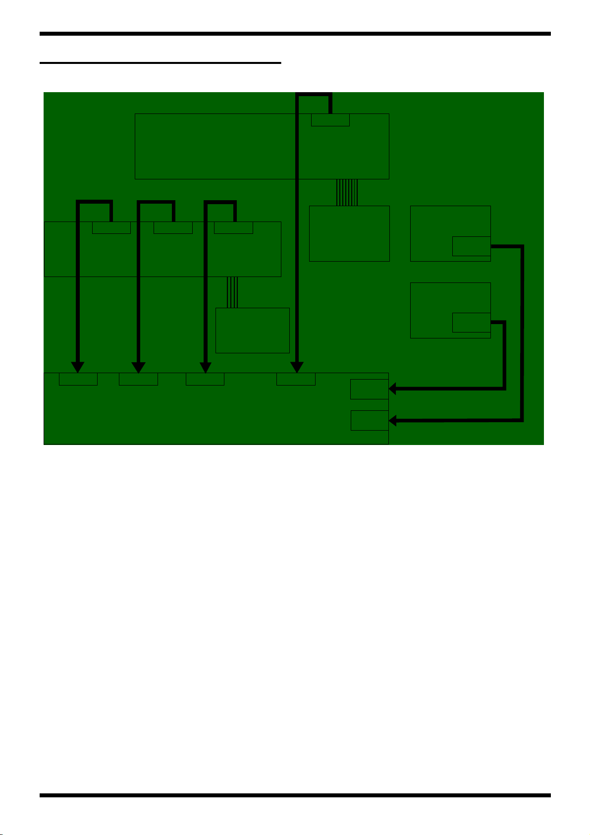
BLOCK DIAGRAM
fig.block
INPUT
SEND
JK11
JK1
JK2
IC5a
JK3
JK4
IC6a IC7a
JK5
JK6
IC6b
R71
VR1b
OUTPUT
VOLUME
TR1
SUB EXP PEDAL
SUB CTL 1,2
PHONES
OUTPUT L
OUTPUT R
EXT OD/DS
RETURN
EXT OD/DS
DIGITAL OUT
IC2bIC1b
IC2a
IC4aVR1a
IC7b
IC17
GT-6 (T)
CN10
CN8
MIDI OUT IN
JK8
CN7
CN6
CN3
IC3
CODEC
AK4552
IC4bIC5b
IC8
CODEC
AK4552
IC19
TC9271FS
IC21 CPU
H8S/2318
IC20 DSP
IC24
DRAM 4M
CN2
CN1
MAIN BOARD ASSY
SW4 BOARD ASSY
CARBON SW
EXP BOARD ASSY
CN4CN4
PEDAL VR
CN11
CN8
CN7
CN2
IC22
SRAM 1M
IC26
Flash 4M
SW 1 BOARD ASSY
PANEL SW,LED
SW 2 BOARD ASSY
PEDAL SW,LED
LCD UNIT
ENC BOARD
ENCODER
CN5
CN6
CN11
CN3
SW 3 BOARD ASSY
PEDAL SW,LED
2 1

Sep. 2 0 0 1 GT-6 (T)
CIRCUIT BOARD (M AIN )
fig.wiring
View from com ponents side
2 322

Sep. 2 0 0 1 GT-6 (T)
CIRCUIT BOARD (M AIN )
fig.sk949-c
View from foil side
2 52 4

SW_SCNA3
SW_DATA7
Contrast
Resister Select
Read/Write
Enable signal
Data Bit 0
Data Bit 1
Data Bit 2
Data Bit 3
Data Bit 4
Data Bit 5
Data Bit 6
Data Bit 7
Sep. 2 0 0 1 GT-6 (T)
CIRCUIT DIAGRAM (M AIN 1 / 2 )
fig.sk961-c
+
IC16D
TC7W04F
D
VCC
GND
IC15
M51953AFP
D3.3
XB
C139
0.1
D
6
RST
+
42
VCC
NC
NC
NC
NC
DLY
67
9
+
D3.3
D3.3
VCC
VSS
R106
4.7K
1
2
3
8
5
84
D
100
VCC
VSS
VSS
20
33
D
C87
0.1
+
5D
R137
10k
1
2
D
+
5D
D8
1SS352
1 2
C90
0.33/50
TC7WH32FU
D
C111 0.1
C112 0.1
C114 0.1
P13/A23/TIOCD0/TCLKB
P12/A22/TIOCC0/TCLKA
PF1/BACK/IRQ1/CS5
PF0/BREQ/IREQ0/CS4
PG1/CS3/IRQ7/CS6
VSS
VSS
VSS
51
70
90
R107
1K
C141
0.1
D
IC28A
TC7WH32FU
7
IC28C
P11/A21/TIOCB0
P10/A20/TIOCA0
D7/PE7
D6/PE6
D5/PE5
D4/PE4
D3/PE3
D2/PE2
D1/PE1
D0/PE0
PF7/PHAI
PF6/AS
PF5/RD
PF4/HWR
PF3/LWR/IRQ3
PF2/WAIT/IRQ2
PG2/CS2
PG3/CS1/CS7
PG4/CS0
HD6412312VF
XA
A19
A18
A17
A16
A15
A14
A13
A12
A11
A10
D15
D14
D13
D12
D11
D10
D9
D8
RES
D3.3
D
A9
A8
A7
A6
A5
A4
A3
A2
A1
A0
+
84
4
3
2
1
55
54
53
52
50
49
48
47
46
45
44
43
41
40
39
38
37
36
35
34
32
31
30
29
28
27
26
25
24
23
22
21
19
18
17
16
71
72
73
74
75
76
64
77
78
96
97
98
99
D3.3
+
D3.3
R129
N.I.U.
C140
0.1
D
1 8
2 7
3 6
4 5
RA7 N.I.U
1 8
2 7
3 6
4 5
RA8 N.I.U
1 8
2 7
3 6
4 5
RA9 N.I.U
1 8
2 7
3 6
4 5
RA10 N.I.U
1 8
2 7
3 6
4 5
RA13 N.I.U
1 8
2 7
3 6
4 5
RA16 N.I.U
1 8
2 7
3 6
4 5
RA17 N.I.U
1 8
2 7
3 6
4 5
RA20 N.I.U
1 8
2 7
3 6
4 5
RA21 N.I.U
R88 N.I.U
R90 N.I.U
+
D3.3
CN5
2.54mm
+
112
2
D3.3
IC27
TC7SH04F
5
6
RA23
N.I.U.
45
36
27
18
45
36
27
18
RA24
N.I.U.
RESET
+
D3.3
RA22
N.I.U.
1 8
2 7
3 6
4 5
RA28 CRN34103J
1 8
2 7
3 6
4 5
R134 10K
R133 10K
R132 10K
AD_C
+
D3.3
R131
N.I.U.
+
+
D3.3
R102
53
10k
2 4
IC28B
TC7WH32FU
3
LCD7
LCD6
LCD5
LCD4
LCD3
LCD2
LCD1
LCD0
LCD_DIR
A19
A18
A17
A16
A15
A14
A19
A18
A17
A16
A15
A14
A13
A12
A11
A10
A9
A8
A7
A6
A5
A4
A3
A2
A1
A0
D
D15
D14
D13
D12
D11
D10
D9
D8
LCD7
LCD6
LCD5
LCD4
LCD3
LCD2
LCD1
LCD0
LCD_DIR
C135
0.1
R130
10K
DIR "H" : A -> B
DIR "L" : A <- B
LCD IF (3.3V <=> 5V)
LCD7
LCD6
LCD5
LCD4
LCD3
LCD2
LCD1
LCD0
D
+
D3.3
0.1
C78
D
10
9
8
7
6
5
4
3
22
2
23
D
TC74VHCT541F
9
8
7
6
D
5
4
3
2
19
1
+
D3.3
R120 10K
A19
IC18
A8
A7
A6
A5
A4
A3
A2
A1
G
DIR
NC
A8
A7
A6
A5
A4
A3
A2
A1
G2
G1
BATT
+
D3.3
+
1
VCCB24VCCA
11
+
20
VCC
10
R119
10K
IC25B
TC75S51F
A18
A17
A16
A15
A14
A13
A12
A11
A10
A9
A8
A7
A6
A5
A4
A3
A2
A1
A0
+
D3.3
D
A19
A18
A17
A16
A15
A14
A13
A12
A11
A10
A9
A8
A7
A6
A5
A4
A3
A2
A1
A0
CS0
RD
CS4
5D
B8
B7
B6
B5
B4
B3
B2
B1
GND
12
D
5D
Y8
Y7
Y6
Y5
Y4
Y3
Y2
Y1
GND
D
A16
A15
A14
A13
A12
A11
A10
A9
A8
A7
A6
A5
A4
A3
A2
A1
A0
D3.3
17
48
1
2
3
4
5
6
7
8
18
19
20
21
22
23
24
25
45
26
11
28
47
14
12
15
1
1
1
1
1
1
1
1
1
1
1
1
1
1
1
1
1
1
1
1
1
1
1
C79 0.1
C91 0.1
+
R80 10k
D3.3
GND13GND
+
52
TA19 Testpin
TA18 Testpin
TA17 Testpin
TA16 Testpin
TA15 Testpin
TA14 Testpin
TA13 Testpin
TA12 Testpin
TA11 Testpin
TA10 Testpin
TA9 Testpin
TA8 Testpin
TA7 Testpin
TA6 Testpin
TA5 Testpin
TA4 Testpin
TA3 Testpin
TA2 Testpin
TA1 Testpin
TA0 Testpin
TCS0 Testpin
TRD Testpin
TCS4 Testpin
D
14
15
16
17
18
19
20
21
IC14
TC74LVXC3245FS
D
11
12
13
14
15
16
17
18
IC22
2
A16
31
A15
3
A14
28
A13
4
A12
25
A11
23
A10
26
A9
27
A8
5
A7
6
A6
7
A5
8
A4
9
A3
10
A2
11
A1
12
A0
30
CE2
22
CE1
29
R/W
24
OE
UPD431000AGW-A10
4
IC25A
TC75S51F
C136
0.1
+
D
IC26
A17
A16
A15
A14
A13
A12
A11
A10
A9
A8
A7
A6
A5
A4
A3
A2
A1
A0
A-1/DQ15
CE
WE
OE
BYTE
WP
RP
RY/BY
LH28F400BVE-BL85
RA26
N.I.U.
RA27
N.I.U.
+
5D
RA1
4 5
3 6
3
1
NC
NC
NC
1 8
2 7
RA3
CRN34104J
4 5
21
D15
20
D14
19
D13
18
D12
17
D11
15
D10
14
D9
13
D8
D15
N.I.U.
1
32
16
R81
1M(F)
R121
4.7M(F)
D
4M Flash
43
41
39
36
34
32
30
44
42
40
38
35
33
31
29
9
10
16
13
37
27
46
TD15Testpin
TD14Testpin
TD13Testpin
TD12Testpin
TD11Testpin
TD10Testpin
TD9Testpin
TD8Testpin
TVCC1Testpin
TVCC2Testpin
TGND1Testpin
TGND2Testpin
CRN34101J
3 6
4 5
1 8
2 7
3 6
4 5
1 8
2 7
3 6
4 5
RA2
CRN34101J
D3.3
13
C118
0.1
D
1 2
CR2032/383-009
D
D15
D14
D13
D12
D11
D10
D9
D8
A19
+
D3.3
C131
0.1
D
1
1
1
1
1
1
1
1
1
1
1
1
1 8
2 7
3 6
4 5
+
12
1 2
R82
10k
BT1
D3.3
1 8
2 7
3 6
+
5D
1 8
2 7
I/O8
I/O7
I/O6
I/O5
I/O4
I/O3
I/O2
I/O1
NC
VDD
VSS
-
+
DQ14
DQ13
DQ12
DQ11
DQ10
DQ9
DQ8
DQ7
DQ6
DQ5
DQ4
DQ3
DQ2
DQ1
DQ0
VPP
VCC
GND
GND
RA4
CRN34101J
D9
RB500V-40
D10
1SS352
+
C126
10/16
D
0.1
C132
D
D15
D14
D13
D12
D11
D10
D9
D8
+
D3.3
D
+
5D
C77
0.1
D
Data Bit 7
Data Bit 6
Data Bit 5
Data Bit 4
Data Bit 3
Data Bit 2
Data Bit 1
Data Bit 0
Enable signal
Read/Write
Resister Select
Contrast
IC20
RA0A-101 (TC223C080AF-101)
+
D3.3
X1
4
VDD
GND2OUT
SG-8002JC(67.7376MHz)
D
C120
0.1
DIF_DATA
DADATB
DADATA
ADDATB
ADDATA
LRCK
BCK
MCK
C133
Q11
10/16
DTA143EKA
D
R101
N.I.U.
C137
N.I.U.
+
5D
C89
0.1
D
OE
1
D
INT0
1
3
R86 N.I.U
R87 N.I.U
R89 N.I.U
R92 N.I.U
R93 N.I.U
R96 N.I.U
R97 N.I.U
R98 N.I.U
+
D3.3
3 2
TO LCD
CN1
A2541WR2-2A16NP
16
16
15
15
14
14
13
13
12
12
11
11
10
10
9
9
8
8
7
7
6
6
5
5
4
4
3
3
2
2
1
1
A13
A12
A11
A10
A9
A8
A7
A6
A5
A4
A3
A2
A1
A0
D15
D14
D13
D12
D11
D10
D9
D8
+
D3.3
R83
N.I.U.
+
D3.3
R105
10K
D
TR1
C81 47/16
C83 0.1
C93 0.1
C96 0.1
C99 0.1
C102 0.1
C105 0.1
C107 0.1
C109 0.1
D
D
PT-10 (13:4)
1020
1
2
3 4
R78
N.I.U
DIF_DATA
D
RES
MUTE
R71
75
6
D
IC17
TC7SH04F
LRCK
BCK
+
D3.3
MCK
IC24
28
A8
27
A7
26
A6
25
A5
24
A4
21
A3
20
A2
19
A1
18
A0
13
NC
14
NC
17
NC
32
NC
16
RAS
30
UCAS
31
LCAS
15
WE
29
OE
D
LC32V4265T-25-TLM
SBT-0180W
+
D3.3
53
D
C97 10/16
I/O16
I/O15
I/O14
I/O13
I/O12
I/O11
I/O10
L15
413
C85
N.I.U.
C86
0.1
24
C101 0.1
D
7
4
6
24
23
22
2
8
25
27
10
5
26
13
14
I/O9
I/O8
I/O7
I/O6
I/O5
I/O4
I/O3
I/O2
I/O1
VCC
VCC
VCC
VSS
VSS
VSS
CONTRAST
C122
10/16
D
81
82
83
84
86
87
88
89
91
92
94
95
96
97
99
100
102
103
104
105
106
107
74
75
77
78
79
65
66
67
68
69
70
71
D
30
118
119
121
122
123
125
126
127
129
130
132
133
134
135
137
138
139
141
76
131
31
+
D3.3
1
6
+
D3.3
R70
Q9
2SC4116GR
R72
10K
C84
0.1
11
26
37
51
73
90
101
109
120
15
22
29
36
44
55
64
72
80
D
470
1
2 3
R74
330
D
D
C92 0.1
C95 0.1
C98 0.1
C100 0.1
C103 0.1
C106 0.1
C108 0.1
C110 0.1
18
59
93
128
140
63
62
61
60
58
57
56
52
53
54
RESET
110
111
112
113
114
115
117
142
143
28
27
25
24
23
21
20
19
17
16
50
49
48
47
46
45
43
42
41
40
39
38
35
ED7
34
ED6
33
ED5
32
ED4
10
ED3
9
ED2
8
ED1
7
ED0
5
4
3
2
12
13
14
85
98
108
116
124
136
144
MAIN BOARD ASSY (Digital)
DIGITAL OUT
JK9A
YKC21-3117
2
1
2
A
10
D
D
+
D3.3
IC19
TC9271FS
30
DATA
LRCK
BCK
CTG3
CTG2
CTG1
UBDA
VLDY
FR32
LBIT
COPY
NC
NC
CKS
XI
43
42
41
40
38
37
36
35
10
9
8
7
5
4
3
2
22
6
1
44
39
23
C123
0.1
VDD
BLOCK
CKA2
CKA1
EMPH
VSS
15
D
RA11
CRN34103J
1 8
2 7
3 6
4 5
1 8
2 7
3 6
4 5
ED7
ED6
ED5
ED4
ED3
ED2
ED1
ED0
+
D3.3
C124
C125
0.1
0.1
DO2
DO1
FS2
FS1
IS2
IS1
M2
M1
LRS
D
JK9B
YKC21-3117
D
17
16
1
12
11
29
28
21
20
19
18
3
9
+
D3.3
RA14
CRN34103J
D3.3
R79
N.I.U
+
D3.3
+
C94
10/16
D
MIDI
JK8
YKF51-5054
14
45
12
INOUT
2
15
24
45
22
2
25
304050
60
D
CN8
53015-0210
1
1
2
2
TO CN10
on SW4 BOARD
CN2
A2001WR2-10P
1
1
2
2
3
3
4
4
5
5
6
6
7
SW_SCAN1
7
8
SW_SCAN0
8
9
9
10
10
TO CN2
on SW2 BOARD
CN7
A2001WR2-8P
1
1
2
2
3
3
4
4
5
5
6
6
7
7
8
8
TO CN11
on SW1 BOARD
CN3
A2001WR2-11P
1
SW_SCAN3
1
2
SW_SCAN2
2
3
SW_SCAN1
3
4
SW_SCAN0
4
5
5
6
SW_DATA5
6
7
SW_DATA4
7
8
SW_DATA3
8
9
SW_DATA2
9
10
SW_DATA1
10
11
SW_DATA0
11
TO CN7
on SW1 BOARD
EXP/CTL 1, 2
JK11
2
3
1
HTJ-064-12D
CN4
A2001WR2-3P
TO CN4
on EXP BOARD
CN6
A2001WR2-7P
TO CN8
on SW1 BOARD
PANEL VR A/D
D
1
1
2
2
3
3
1
1
2
2
3
3
4
4
5
5
6
6
7
7
L17
N.I.U.
D
+
D3.3
LED_DATA3
LED_CLOCK
SW_SCAN3
SW_SCAN2
SW_DATA7
SW_DATA6
+
D3.3
C116
10/16
D
LED_DATA4
LED_DATA2
LED_DATA1
LED_CLOCK
D
+
D3.3
+
D3.3
C75
N.I.U.
C104
10/16
D
R84
470k
R91
4.7k
R111
4.7K
C138
0.1
D
L12
L13
N.I.U
N.I.U
L14
L16
N.I.U
1 2
D11
1SS352
D3.3
R110
4.7K
D3.3
+
D3.3
D
D
N.I.U
ENC_B
ENC_A
+
DA3 1SS302
2 1
+
DA4 1SS302
2 1
D
AD1
AD0
R138 N.I.U.
R75 22 1/2W
R135 N.I.U
SW_DATA7
SW SCAN
RA18
CRN34103J
3
3
R94
4.7K
D3.3
R100
1K
+
1 8
D
D
2 7
R77 22
R136 N.I.U
SW_SCNA3
SW DATA
1 8
2 7
3 6
R85
4.7K
RA25
N.I.U.
3 6
4 5
R67 120
R69
100
Q10
N.I.U.
+
D3.3
2 1
LED DATA
RA5
CRN34104J
IC29
TC74HC238AF
4 5
1 8
2 7
3 6
MUTE
MUTE
C127
0.001
D
C128
0.1
D
C134
0.1
D
AD_C
AD_B
AD_A
D6
1SS352
1 2
+
D3.3
1
3 2
R73
N.I.U.
3
DA5 N.I.U
RA6
CRN34101J
1 8
2 7
3 6
4 5
R108 100
D3.3
7
Y7
9
Y6
10
Y5
11
Y4
12
Y3
13
Y2
14
Y1
15
Y0
RA12 CRN34101J
4 5
3 6
2 7
1 8
1 8
2 7
3 6
4 5
RA15 CRN34101J
RA19
CRN34103J
4 5
D
CONTRAST
BATT
+
D3.3
IC16A
TC7W04F
+
D3.3
1 8
+
16
VCC
GND
8
D
R95
N.I.U
C129
0.01
R99
N.I.U
ENC_B
ENC_A
D3.3
1
3
IC13
PC400
C82
N.I.U.
D7
N.I.U.
1 2
D
17
D
2 7
3 6
4 5
AD_B
C142
0.1
D
3
C
2
B
1
A
5
G2B
4
G2A
6
G1
X2
MA-406 (20MHz)
C121 15P
D
D
C130
0.01
+
6
4
5
R76
10k
35
IC16B
TC7W04F
D3.3
+
D3.3
R117 N.I.U.
C119
15P
D3.3
C143
10/16
D
ENCODER
D
+
D3.3
+
R116
100k
R118 N.I.U.
AD_A
+
+
D3.3
MIDI IN
C80
0.1
1 4
R109 10
C115
0.1
R68
2.2k
INT0
D3.3
D3.3
+
D3.3
+
+
R103
4.7K
C88
0.1
IC16C
TC7W04F
+
15
14
13
12
11
10
8
7
6
5
95
94
93
92
91
61
58
57
56
65
69
68
79
80
88
87
86
85
84
83
82
81
89
D
62
66
63
60
59
D
R104
1K
5D
62
7
4
D
RESET
C113
10/16
D
IC21
IRQ5/SCK1/P35
IRQ4/SCK0/P34
RXD1/P33
RXD0/P32
TXD1/P31
TXD0/P30
P17/TIOCB2/TCLKD
P16/TIOCA2
P15/TIOCB1/TCLKC
P14/TIOCA1
PG0/ADTRG/IRQ6
P27/TIOCB5/TMO1
P26/TIOCA5/TMO0
P25/TIOCB4/TMCI1
P24/TIOCA4/TMRI1
P23/TIOCD3/TMCI0
P22/TIOCC3/TMRI0
P21/TIOCB3
P20/TIOCA3
NMI
EXTAL
XTAL
AVCC
VREF
P47/AN7/DA1
P46/AN6/DA0
P45/AN5
P44/AN4
P43/AN3
P42/AN2
P41/AN1
P40/AN0
AVSS
WDTOVF(FWE*)
STBY
MD2
MD1
MD0
2 726

Sep. 2 0 0 1 GT-6 (T)
CIRCUIT DIAGRAM (M AIN 2 / 2 )
fig.block
12
1
IC1A
M5238FP
1
A
1
A
1
A
1
A
12
R46
220k
A
D2
1N4004
D4
1N4004
D5
1N4004
C2
N.I.U.
R3 18k
C4
7
A+9
84
-
+
A-9
R11
47/2W
R14
47/2W
R22
1k
R33
1k
1
R128
+
N.I.U.
L10 N.I.U.
R141
10 (0805size)
R139
10 (0805size)
10/16
IC1C
M5238FP
C39
10/16
R143
N.I.U.
R62
0.68 (1/2W)
R114
4.7k
R115
4.7k
C158
N.I.U.
A
IC7C
NJM2100M
C57
N.I.U.
D
100/35
100/35
-
+
IC9
NJM2374AM
Q13
2SD1664
C64
C74
2 3
Q14
2SB1132
6
-
5
+
IC1B
M5238FP
R7
1M
A
C37
N.I.U.
R42 18k
2
-
3
+
IC6A
M5218AFP
C56
2200/35
D
C65
470/35
C71
470/35
12
C13
47/16
R24
10K
A
100/16
R35
10K
A
R48
84
10K
R52
10K
A A
7
SI
6
V+
32
1
1
C21
100/16
C31
C14
0.1
8
CD
GND
4
D
100/35
100/35
R5 100K(F)
R10 6.8K(F)
C67
C70
C3 10P
R4 12K(F)
IC2A
1
+
C6 10P
R8 12K(F)
7
+
84
-
IC2C
NJM2100M
+
A
R16
10K
2
-
3
+
R27
10K
6
-
5
+
R44 100K(F)
R53 6.8k(F)
R113
1k
Q12
2SA1241-Y
1
2 3
470uH(TSL1112SRA-471KR72)
D
D3
SS14
1 2
D
R65
1.5k
D13
RD10ESAB2
1 2
D14
RD10ESAB2
1 2
R66
1.8k
NJM2100M
IC2B
NJM2100M
R20
47K
IC5A
M5216F
A
RK09K12A0 (10kAx2)
R31
47K
A
RK09K12A0 (10kAx2)
R43 12K(F)
2
3
R50 12K(F)
6
5
R63 3k(F-rank)
R64
1.8k(F-rank)
D
Q7
2SD1758
32
1
C68
100/16
C69
100/16
1
2 3
Q8
2SB1182
R127
N.I.U.
C157
100/16
A
C18
10/16
VR1A
A
C28
10/16
VR1B
C38 10P
1
+
IC7A NJM2100M
C42 10P
7
+
IC7B NJM2100M
L11
C61
470/6.3
C162
0.1
C163
0.1
+
1
+
D3.3
R15
82K
C16 10P
C19
1
10/16
IC4A
M5218AFP
C29
10/16
220/35
D
D
IC4B
M5218AFP
C144
R26
82K
C25
10P
7
+
C48
0.1
R140
10 (0805size)
13
23
22 12
10
20
A
C152
10/16
C153
10/16
D12
1 2
1N4004
A+9
C66
100/16
A
C72
100/16
A-9
2
3
6
5
R12
10K
R13
10K
A
C15
0.001
R17 47K
C145 10p
1
C23
150P
C24
R25
0.001
330
R28 47K
A
C146 10p
7
C33
IC5B
150P
M5216F
R36
330
A
C44
C45
0.1
47/16
R112
2.2k
1
CS
2
ES
5
IN+
CT
3
C62
150p
D
-
+
-
+
2
3
6
5
L8 N.I.U
C150
10/16
C151
10/16
R18
N.I.U
A
R29
N.I.U
A
R54
10
C49
10/16
A
C58
0.1
C159
0.1
R19
10K
C17
C22
N.I.U.
A
C32
N.I.U.
A
C50
0.1
IC30 N.I.U.
IC31 S-81233SGY
R30
10K
D
C51
10/16
IC10
BA17805FP
IN1OUT
COM
2
DD
IN2OUT
COM
1
D
IN2OUT
COM
1
D
10/16
C26
10/16
2
1
15
16
4
5
3
A
IC8
AK4552VT
LIN
RIN
LOUT
ROUT
VA
VD
VSS
3
3
3
L2
+
N.I.U
R9
MCLK
SDTO
BCLK
LRCK
SDTI
PDN
DEM0
DEM1
VCOM
+
5D
A
D
+
C8
10/16
IC5C
M5216F
C60
N.I.U.
C161
N.I.U.
10
C9
0.1
A+9
84
-
+
A-9
11
8
12
10
9
13
6
7
D
14
C52
10/16
C76
47/16
D
R142
1.5k
A
C7
0.1
C59
0.1
C160
0.1
D
C10
10/16
IC3
AK4552VT
2
LIN
1
RIN
15
LOUT
16
ROUT
4
VA
5
VD
3
VSS
A
C147
0.1
A D
C148
0.1
A D
C149
0.1
A D
C27
10/16
A
C34
10/16
MCK
ADDATB
BCK
LRCK
DADATB
RES
C53
0.1
A
A+9
84
-
+
A-9
IC4C
M5218AFP
R51 33k
R57 33k
IC6C
M5218AFP
MCLK
SDTO
BCLK
LRCK
SDTI
PDN
DEM0
DEM1
VCOM
C154
10p
11
8
12
10
9
13
6
7
D
14
C11
10/16
A+9
84
-
+
A-9
R47
10k
R49 47k
6
5
C54
R60
0.001
47k
R61
10k
A
C12
0.1
A
C41
10P
-
+
C43
0.001
7
IC6B
M5218AFP
D
MCK
ADDATA
BCK
LRCK
DADATA
RES
C35
470/6.3
C46
10/16
+
D3.3
12
D1
1SS352
3 2
Q5
2SA1586GR
R39
1M
A-9
R55
1K
+
D3.3+D3.3
R123
R124
47k
R122
R37
47k
1
23
1
10k
A
Q6
RN1441-A
C47 10/16
R58
100K
A A
3 2
R38
10K
Q15
2SA1586GR
D
R59
100K
47k
1
R56
1K
L9
N.I.U
MUTE
2
4
1
A
JK6
SEND
HTJ-064-12i
MAIN BOARD ASSY (Analog)
GUITAR IN
HEADPHONES
OUT L
(MONO)
OUT R
RETURN
JK1
HTJ-064-12i
JK2
HTJ-064-12D
JK3
HTJ-064-12i
JK4
HTJ-064-12i
JK5
HTJ-064-12i
JK7
2
1
3
HEC0740-010010
2
4
1
2
4
1
L1
N.I.U
2
4
1
A
2
3
1
A
A
A
L7
N.I.U
2
4
1
A
DSS9ND31H223Q91J
DSS9ND31H223Q91J
C1
R1
0.01
1.2K
R2 10K
A
R6
10K
A+9
3
2 1
DA1
N.I.U.
L3
N.I.U
L4
N.I.U
L5
R21
N.I.U
1k
R32
1k
L6
N.I.U
R45
10K
A+9
3
2 1
DA2
N.I.U.
FL1
C55
ERZVA7V330
D
FL2
D
C5
0.1(P)
A-9
C20
10/16
R23
100k
A
C30
10/16
R34
100k
A
A
C40
10/16
A-9
SW1A
SDKLA1-B
1 2
Q1
RN1441-A
Q2
RN1441-A
Q3
RN1441-A
Q4
RN1441-A
C36
0.01
R41 10k
D17
1SS352
D16
1SS352
2
3
A
-
+
2 3
2 3
2 3
2 3
R40 1.2k
1 2
1 2
2 928

Sep. 2 0 0 1 GT-6 (T)
CIRCUIT BOARD (SW SHEET)
fig.block
View from com ponents side
View from com ponents side
3 130

SW_DATA6
SW_DATA7
SW_SCAN0
SW_SCAN1
SW_SCAN2
SW_SCAN3
SW_DATA7
SW_SCAN1
SW_SCAN2
Sep. 2 0 0 1 GT-6 (T)
CIRCUIT DIAGRAM (SW SHEET)
EXP BOARD ASSY (6/6)
CN4
WIRING 3P
1
1
2
2
3
3
TO CN4 ON MAIN BOARD
ENC BOARD ASSY (5/6)
EN1A
EN
EVE GC1 F20 24B
A B
123
3
11223
11223
3
D
+
CN11
WIRING 8P
CN7
WIRING 11P
CN8
WIRING 7P
TO CN6 ON MAIN BOARD TO CN3 ON MAIN BOARD TO CN7 ON MAIN BOARD
D3.3
1
1
2
2
3
4
5
6
7
8
1
2
3
4
5
6
7
8
9
10
11
1
2
3
4
5
6
7
D
3
4
5
6
7
8
1
SW_SCAN3
2
SW_SCAN2
3
SW_SCAN1
4
SW_SCAN0
5
6
SW_DATA5
7
SW_DATA4
8
SW_DATA3
9
SW_DATA2
10
SW_DATA1
11
SW_DATA0
D
FER+3.3
1
2
AD1
3
AD0
4
AD_C
5
AD_B
6
AD_A
7
D
D+3V
VR1A
RK11K1140 (10KSB)
121314
11
DGND
10
EN
A B
EN1B
EVE GC1 F20 24B
CN5
RIBON 3P (1/2)
RIBON CABLE (3P)
CN6
RIBON 3P (1/2)
DGND
BANK
DOWN
+
D3.3
12
LED8
L-34HDSL
R8
390
BANK DOWN BANK UP
SW6
1 2
1 2
1SS133
SKQKAH
MANUAL
NAME/FV/
CHAIN/NS
LED9
L-312LRD
D3.3+D3.3+D3.3+D3.3+D3.3+D3.3+D3.3+D3.3+D3.3+D3.3+D3.3+D3.3
LED10
L-312LRD
+
12
R9
390
PRE/SP
TYPE VARIATION
+
D3.3
3
Q1
2 1
RN2207
R21
120
R31 470
R32 470
R33 470
R34 470
R35 470
R36 470
R37 470
R38 470
R39 470
R40 470
R41 470
R42 470
R43 470
R44 470
12
R10
390
3
D5
SW5
1 2
1SS133
SW14
1 2
SKQKAB
TUNER/
BYPASS
SW20
1 2
SKQKAB
MANUAL
SW26
1 2
SKQKAB
SW_DATA4
PRE/SP
BASS
3
2
1
VR8
RD901-40-125F-B54-00D
PATCH
LEVEL
FER+3.3
3
2
1
VR15
RD901-40-125F-B54-00D
"CTL""4""3""2""1"
+
D3.3
12
LED5
L-34HDSL
R5
390
SW_SCAN3
SW_SCAN2
SW_SCAN1
SW_SCAN0
SW_DATA6
CN2
WIRING 10P
D14
1 2
1SS133
D20
1 2
1SS133
D26
1 2
1SS133
RD901-40-125F-B54-00D
D
SW_DATA7
SW_DATA5
DATA5
PRE/SP
MIDDLE
2
9
10
10
TO CN2 ON
MAIN BOARD
VR9
3
1
CN1
RIBON 7P (1/2)
+
D3.3
+
D3.3
D
11223344556677889
LED_DATA1
LED_DATA2
LED_DATA4
1
1
2
2
3
3
4
4
5
5
6
6
7
7
2
3
2
3
CN3
RIBON 7P (1/2)
RIBON CABLE (7P)
2
DATA
3
CLOCK
D3.3
C2
0.1
D
DATA
CLOCK
D3.3
C5
0.1
D
DATA
CLOCK
1
1
2
2
3
3
4
4
5
5
6
6
7
7
D3.3
C1
0.1
D
16
1
+
IC3
BU2090 (DIP)
16
Q11
Q10
VDD
Q9
Q8
Q7
Q6
Q5
Q4
Q3
Q2
Q1
Q0
VSS
1
D
+
IC6
BU2090 (DIP)
16
Q11
Q10
VDD
Q9
Q8
Q7
Q6
Q5
Q4
Q3
Q2
Q1
Q0
VSS
1
D
+
D3.3
SW_SCAN1
SW_SCAN2
SW_DATA7
SW3 BOARD ASSY (3/6)
+
IC2
BU2090 (DIP)
15
Q11
14
Q10
VDD
13
Q9
12
Q8
11
Q7
10
Q6
9
Q5
8
Q4
7
Q3
6
Q2
5
Q1
4
Q0
VSS
D
15
14
13
12
11
10
9
8
7
6
5
4
11
10
9
6
7
5
4
14
13
12
8
15
+
D3.3
+
D3.3
IC1
BU2090F (SOP)
16
15
Q11
14
Q10
VDD
13
Q9
12
DATA
CLOCK
1 2
1 2
1 2
1 2
1
D9
1SS133
D15
1SS133
D21
1SS133
D27
1SS133
Q8
Q7
Q6
Q5
Q4
Q3
Q2
Q1
Q0
VSS
D
SW1
1 2
SKQKAH
DATA0
11
10
9
8
7
6
5
4
1 2
1 2
1 2
1 2
SW_DATA0
2
3
20
OD/DS
SW9
SCAN3
SW_SCAN3
SCAN2
SW_SCAN2
1 2
SKQKAB
OD/DS
TYPE VARIATION
SW15
1 2
SKQKAB
PRE/SP
SW21
SCAN1
SW_SCAN1
SW_SCAN0
1 2
SKQKAB
PRE/SP
TYPE VARIATION
SW27
1 2
SKQKAB
12
LED1
L-34HDSL
R1
390
LED_DATA3
D1
D10
1 2
1SS133
D16
1 2
1SS133
D22
1 2
1SS133
D28
1 2
1SS133
SW2
1 2
SKQKAH
SW_DATA1
DATA1
1 2
1SS133
DELAY WAH
SW10
SKQKAB
REVERB EQ EXIT WRITE
SW16
SKQKAB
DELAY
TAP
SW22
SKQKAB
CHORUS SFX-2
SW28
SKQKAB
1 2
1SS133
SW11
1 2
SKQKAB
SW17
1 2
SKQKAB
SFX-1
SW23
1 2
SKQKAB
SW29
1 2
SKQKAB
D2
+
D3.3
12
1 2
D11
1 2
1SS133
D17
1 2
1SS133
D23
1 2
1SS133
D29
1 2
1SS133
LED2
L-34HDSL
R2
390
SW3
SKQKAH
SW_DATA2
DATA2
D3
1 2
1SS133
PARAMETER
[<](LEFT)
SW12
1 2
SKQKAB
SW18
1 2
SKQKAB
PEDAL
ASSIGN
SW24
1 2
SKQKAB
NAME/FV/
CHAIN/NS
SW30
1 2
SKQKAB
+
D3.3
12
LED3
L-34HDSL
R3
390
+
D3.3
12
LED4
L-34HDSL
R4
390
SW2 BOARD ASSY (2/6)
"CTL""4""3""2""1"
D4
SW4
1 2
1 2
1 2
SW13
SW19
SW25
SW31
D13
1 2
1SS133
D19
1 2
1SS133
D25
1 2
1SS133
D31
1 2
1SS133
SKQKAH
1SS133
PARAMETER
[>](RIGHT)EZTONE
SKQKAB
SKQKAB
OUTPUT
SELECT
SKQKAB
UTILITY
SKQKAB
DATA4
D12
1 2
1SS133
D18
1 2
1SS133
1 2
1SS133
1 2
1SS133
D24
D30
SKQKAH
SW_DATA3
DATA3
1 2
1 2
1 2
1 2
[6detents] [11detents]
IC4
TC74HC4051AP
3
COM
+
D3.3
16
VCC
C3
0.1
8
GND
7
VEE
D D
IC5
TC74HC4051AP
3
COM
+
D3.3
16
VCC
C4
0.1
8
GND
7
VEE
D
OD/DS
DRIVE
4
7
2
6
5
5
1
4
12
3
15
2
14
1
13
0
9
C
10
B
11
A
6
INH
4
7
2
6
5
5
1
4
12
3
15
2
14
1
13
0
9
C
10
B
11
A
6
INH
D
2
RD901-40-125F-B54-00D
RD901-40-125F-B54-00D
OD/DS
TYPE
RD901-40-125F-B54-06D
FER+3.3 FER+3.3 FER+3.3 FER+3.3 FER+3.3 FER+3.3 FER+3.3 FER+3.3
3
2
1
D D D D D D D D
VR2
VR3
3
1
RD901-40-125F-B54-00D
OD/DS
LEVEL
2
VR4
3
1
PRE/SP
TYPE
VR5
RD901-40-125F-B54-11D
3
2
1
RD901-40-125F-B54-00D
PRE/SP
TREBLE
RD901-40-125F-B54-00D
3
2
1
VR6
PRE/SP
GAIN
VR7
3
2
1
[6detents]
DELAY
LEVEL
2
REVERB
DELAY
LEVEL
FEEDBACK
VR10
RD901-40-125F-B54-00D
FER+3.3 FER+3.3
VR16
FER+3.3
3
1
D
3
2
1
RD901-40-125F-B54-00D
2
CHORUS
LEVEL
RD901-40-125F-B54-00D
FER+3.3 FER+3.3
3
2
1
D
VR11
PRE/SP
LEVEL
VR12
FER+3.3
3
1
RD901-40-125F-B54-00D
3
2
1
DD
VR13
D
PRE/SP
SPEAKER
VR14
RD901-40-125F-B54-06D
3
2
1
D
BANKUPEXP PEDAL FX
D3.3
D6
1 2
SKQKAH
UTILITY EQ SFX-1 SFX-2 CHORUS REVERB
LED11
L-312LRD
12
(RED)(GREEN) (RED)(GREEN)
+
D3.3
3
Q2
RN2207
2 1
R22
390
12
LED27
L-3WSRSGW-CC
D
SW7
+
12
R11
390
D3.3
ON/OFF
LED7
L-34HDSL
R7
390
D7
1 2
1SS133
LED12
L-312LRD
12
R12
390
OD/DS
TYPE VARIATION
D3.3
3
R23
120
LED29 A-552SR BW
+
14
DIG1
D3.3
LED13
L-312LRD
12
+
Q3
2 1
RN2207
A116B1
15
+
12
R13
390
3
LED6
L-34HDSL
R6
390
LED14
L-312LRD
12
D3.3
3
12
LED28
L-3WSRSGW-CC
D
C13D1
2
LED15
L-312LRD
12
R14
R15
390
390
+
WAH EZ TONE TUNER/
Q4
LED21
RN2207
L-312LRD
2 1
D3.3
R24
390
G117DP1
E11F1
4
18
SW SHEET ASSY
CN10
WIRING 2P
1
1
2
2
TO CN8 ON MAIN BOARD
SW4 BOARD ASSY (4/6)
DELAY
DELAY PRE/SP OD/DS
TAP
LED16
LED17
L-312LRD
12
R17
390
C28D2
6
BYPASS
LED18
L-312LRD
12
LED23
L-312LRD
+
D3.3+D3.3
12
R27
390
E25F2
12
L-312LRD
+
12
R25
390
12
R16
390
LED22
L-312LRD
D3.3
A211B2
+
12
R26
390
10
EXP PEDAL FX
ON/OFF
SW8
1 2
CARBON SW
LED19
L-312LRD
12
R18
R19
390
390
PEDAL
ASSIGN
LED24
L-312LRD
12
R28
390
13
DIG2
G2
DP
7
9
F
E
OUTPUT
SELECT
LED25
L-312LRD
+
D3.3
12
+
D3.3
A
G
D
LED20
L-312LRD
12
R20
390
R29
390
B
C
DP
SW1 BOARD ASSY (1/6)
3 332

Sep. 2 0 0 1
ERROR M ESSAGE
N orma l Error M essage
fig.EM-1
The memory backup battery inside the GT-6 has run down. (This message will
appear when the power is turned on.)
Replace the battery as soon as possible. For battery replacement, please contact
a nearby Roland service center or your dealer.
fig.EM-2
There is a problem with the MIDI cable connection.
Check to make sure the cable has not been pulled out or is not shorted.
fig.EM-3
BATTERY check
fig.EM-3
“LOW” is displayed when 2.7 V or lower.
fig.EM-4
“No Battery !!” is displayed when a battery is not inserted.
* Insert a new lithium battery.
If an error message continues to appear when a new lithium battery is
inserted, check the following parts and wiring.
CPU(IC21):pin 84
OP.Amp(IC25):pins 1-5
Resistor(R80, R81, R82, R121)
Diode(D9, D10)
Capacitor(C118, C136)
M IDI Check
fig.EM-5
You’ve attempted to switch patches by rotating the [PATCH/VALUE] dial,
but the Dial function (p. **) is set to “VALUE Only.”
If you want to be able to switch patches using the [PATCH/VALUE] dial, set
the Dial function to “PATCH No.& VALUE.”
fig.EM-4
More MIDI messages were received in a short time than could be processed
correctly.
Error messages in test mode
DSP check
fig.EM-1
Problem : The data written in the DSP (IC8) PROM and the data read do not
match.
* Check the following parts and wiring.
DSP(IC20): pins 77-79, 81-84, 86-89, 91-92, 94-97, 99-100, 102-107
fig.EM-2
Problem : No MIDI cables are connected.
fig.EM-6
Problem : The data sent (MIDI OUT) and the data received (MIDI IN) do not
match.
* Check the following parts and wiring.
• MIDI IN
CPU(IC21):pin 12
Resister(R67-R69)
Capacitor(C80)
Photo Coupler(IC13)
Diode(D6)
• MIDI OUT
CPU(IC21):pins 10
Resister(R76,R77,R138)
Gate IC(IC16)
DSP Pitch inter r uption signa l check
fig.EM-7
Problem : The data written to the DRAM (IC24) via the DSP (IC20) and the
data read do not match.
* Check the following parts and wiring.
DSP(IC20): pins 7-10, 12-14, 16, 17, 19-21, 23-25, 27, 32-35
DRAM(IC24): pins 1-44
3 4
Problem : The interruption signal generated from DSP (IC8) internal oscillation
is not recognized.
* Check the following parts and wiring.
CPU(IC21):pin 8
DSP(IC20):pin 75
 Loading...