

Page 1
MCR01
Resistors
Thick film rectangular
MCR01 (1005 size : 1 / 16W)
zFeatures
1) Extremely small light
Area ratio is 60% smaller than that of chip 1608, while weight ratio has been cut 75%.
2) Highly reliable chip resistor
Ruthenium oxide dielectric offers superior resistance to the elements.
3) Electrodes not corroded by soldering
Thick film makes the electrodes very strong.
4) Flat surface further facilitates mounting
Mounting can also be automated.
5) ROHM resistors have approved ISO–9001 certification.
Design and specifications are subject to change without notice. Carefully check the specification sheet supplied with the
product before using or ordering it.
zRatings
Item Conditions Specifications
Rated power
Rated voltage
Nominal resistance See Table 1.
Operating temperature
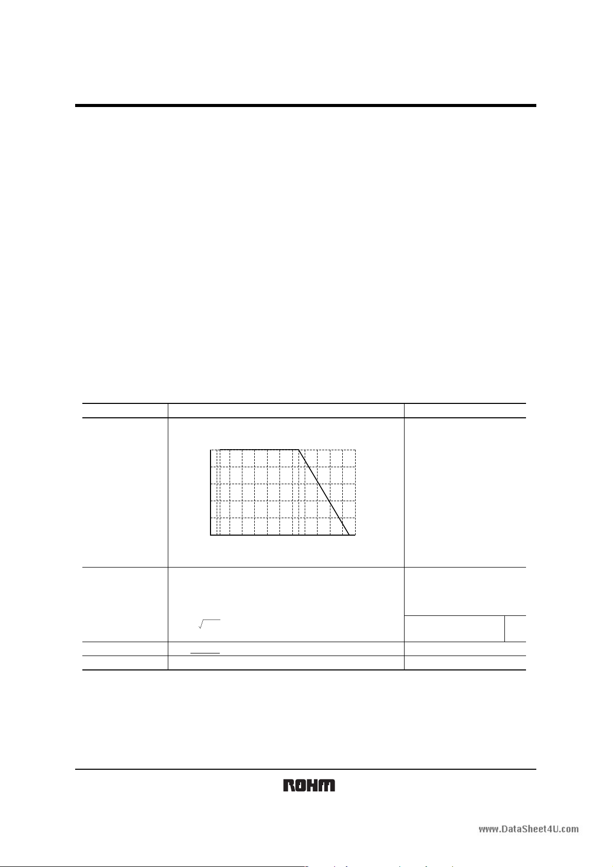
Power must be derated according to the power derating curve in
Figure 1 when ambient temperature exceeds 70°C.
100
80
60
40
POWER LOAD (%)
20
0
The voltage rating is calculated by the following equation.
If the value obtained exceeds the limiting element voltage,
the voltage rating is equal to the maximum operating voltage.
E= P×R
−55 0 70 100 125 155
AMBIENT TEMPERATURE (°C)
Fig.1
E: Rated voltage (V)
P: Rated power (W)
R: Nominal resistance (Ω)
0.063W (1 / 16W)
at 70°C
Limiting element voltage 50V
−55°C to +155°C
Rev.A 1/5
Page 2
MCR01
Resistors
Jumper type
Resistance
Rated current
Operating temperature
zBefore using components in circuits where they will be exposed to transient s such as pulse loads (short–duration, high– level loads), be cert ain to
evaluate the component in the mounted state. In addition, the reliability and performance of this component cannot be guaranteed if it is used with
a steady state voltage that is greater than its rated volt age.
z
Characteristics
Table 1
Max. 50mΩ
1A
−55°C to +155°C
Resistance tolerance
J (±5%)
F (±1%)
D (±0.5%)
Resistance range
(Ω)
1.0≤R<10 +500 / −250
10≤R≤10M
10≤R≤2.2M
10≤R<100
100≤R≤1MΩ
(E24)
(E24)
(E24)
(E24)
(E24)
Resistance temperature coefficient
(ppm / °C)
±200
±100
±100
±50
Item Test conditions (JIS C 5201-1)
Resistance
Variation of resistance
with temperature
Overload
Solderability
Resistance to
soldering heat
Rapid change of
temperature
Damp heat, steady state
Endurance at 70°C
Endurance
Resistance to solvent
Bend strength of
the end face plating
Resistor type
J : ±5%
F : ±1%
D : ±0.5%
± (2.0%+0.1Ω) Max. 50mΩ
A new uniform coating of minimum of
95% of the surface being immersed
and no soldering damage.
± (1.0%+0.05Ω)
No remarkable abnormality on the appearance.
± (1.0%+0.05Ω)
± (3.0%+0.1Ω)
± (3.0%+0.1Ω)
± (3.0%+0.1Ω)
± (1.0%+0.05Ω)
± (1.0%+0.05Ω)
Without mechanical damage such as breaks.
Guaranteed value
Max. 50mΩ
See Table.1
Max. 50mΩ
Max. 50mΩ
Max. 50mΩ
Max. 50mΩ
Max. 50mΩ
Max. 50mΩ
Max. 50mΩ
Jumper type
JIS C 5201-1 4.5
JIS C 5201-1 4.8
Measurement : +25 / +125°C
JIS C 5201-1 4.13
Rated voltage (current) ×2.5, 2s.
Limiting Element Voltage×2 : 100V
JIS C 5201-1 4.17
Rosin·Ethanol (25%WT)
Soldering condition : 235±5
Duration of immersion : 2.0±0.5s.
JIS C 5201-1 4.18
Soldering condition : 260±5
Duration of immersion : 10±1s.
JIS C 5201-1 4.19
Test temp. : −55
JIS C 5201-1 4.24
°C, 93%RH
40
Test time : 1,000h to 1,048h
JIS C 5201-1 4.25.1
Rated voltage (current), 70
1.5h : ON − 0.5h : OFF
Test time : 1,000h to 1,048h
JIS C 5201-1 4.25.3
°C
125
Test time : 1,000h to 1,048h
JIS C 5201-1 4.29
23±5
°C
, Immersion cleaning, 5±0.5min.
Solvent : 2-propanol
JIS C 5201-1 4.33
°C
to +125°C 5cyc
°C
°C
°C
Rev.A 2/5
Page 3

Resistors
zExternal dimensions (Unit : mm)
1
0.2±0.1
+0.05
0.25
−0.1
1.0±0.05
6
2
3
No.
1
4
5
0.35±0.05
0.5±0.05
Thick dielectric glaze of oxide metal (only silver used for jumper)
2
Thick film of silver for electrode
3
Nickel-coated electrode
4
External electrode coated with Sn
5
Alumina substrate
6
Overcoating
z
Packaging
Reel Taping
ABD
0 2
0 4
0 6
0 8
C
ABCD
φ180
0
−1.5
φ60
+1
0
9
+1.0
0
Label
(Unit : mm)
±
0.2
φ13
0 2
0 4
0 6
0 8
EIAJ ET-7200B compliant
Material
P0
P
2
A
0
B
0
P
1
Heat crimp cover/Tape
Thick paper
(Underside paper tape) Chip resistor Square punchout hole
mount
WFEA0B
8.0±0.3 3.5±0.05 1.75±0.1 0.7±0.1 1.2±0.1
D
0
P
0
P
1
φ1.5
+0.1
4.0±0.1 2.0±0.05 2.0±0.05
0
MCR01
φD
0
P
2
F
(Unit : mm)
0
T
2
Max. 1.1
E
W
T
2
Rev.A 3/5
Page 4

Resistors
zPart designation
Part No.
MCR01
3-digit or 4-digit IEC coding system
Nominal resistance
Packaging specifications code
Part No. Code Packaging style
MZPMCR01
zDimensions
1.20
1.15
1.10
1.05
1.00
0.95
LENGTH (mm)
0.90
0.85
0.80
10 100 1k 10k 100k 1M
Fig.2 Dimensions (length)
JIS C 5201-1 4.4.2
SAMPLE SIZE : n=20pcs
MICROMETER
RESISTANCE
z
Electrical characteristics
8.0
6.0
4.0
2.0
0
– 2.0
DC RESISTANCE (%)
– 4.0
– 6.0
– 8.0
10 100 1k 10k 100k 1M
JIS C 5201-1 4.5
SAMPLE SIZE : n=20pcs
20°C 65%RH
RESISTANCE (Ω)
Fig.5 Resistance
(Ω)
Paper tape
Basisic ordering
unit (pcs)
10,000
0.70
0.65
0.60
0.55
0.50
0.45
WIDTH (mm)
0.40
0.35
0.30
10 100 1k 10k 100k 1M
(ppm/°C)
TEMPERATURE COEFFICIENT
Fig.3 Dimensions (width)
800
600
400
200
0
−200
−400
−600
−800
10 100 1k 10k 100k 1M
JIS C 5201-1 4.4.2
SAMPLE SIZE : n=20pcs
MICROMETER
RESISTANCE
JIS C 5201-1 4.8
SAMPLE SIZE : n=10pcs
25°C / 125°C
RESISTANCE
Fig.6 Variation of resistance with
temperature
Resistance tolerance
F ±1% ±5%J ±0.5%D
Specify "J" for jumper also.
THICKNESS (mm)
(Ω)
(%)
∆R/R
−1.0
−2.0
−3.0
−4.0
(Ω)
0.55
0.50
0.45
0.40
0.35
0.30
0.25
0.20
0.15
10 100 1k 10k 100k 1M
JIS C 5201-1 4.4.2
SAMPLE SIZE : n=20pcs
MICROMETER
RESISTANCE
Fig.4 Dimensions (thickness)
4.0
3.0
2.0
1.0
0.0
10 100 1k 10k 100k 1M
JIS C 5201-1 4.13
SAMPLE SIZE : n=10pcs
RATED VOLTAGE × 2.5TIMES : 2s
LIMITING ELEMENT VOLTAGE : 100V
RESISTANCE
(Ω)
Fig.7 Overload
(Ω)
Rev.A 4/5
Page 5

Resistors
2.0
1.5
1.0
0.5
(%)
0.0
∆R/R
−0.5
−1.0
−1.5
−2.0
JIS C 5201-1 4.18
SAMPLE SIZE : n=10pcs
SOLDERING CONDITION
: 260°C 10s
10 100 1k 10k 100k 1M
RESISTANCE
(Ω)
Fig.8 Resistance to soldering heat
4.0
3.0
2.0
1.0
(%)
0
∆R/R
−1.0
−2.0
−3.0
−4.0
10 100 1k 10k 100k 1M
JIS C 5201-1 4.25.1
SAMPLE SIZE : n=10pcs
70°C 1,000h
OVERLOAD : THE RATED VOLTAGE
RESISTANCE
(Ω)
Fig.11 Endurance at 70°C
2.0
1.5
1.0
0.5
(%)
0.0
∆R/R
−0.5
−1.0
−1.5
−2.0
10 100 1k 10k 100k 1M
Fig.14 Bend strength of
JIS C 5201-1 4.33
SAMPLE SIZE : n=10pcs
ENDURANCE WITH 90mm WIDTH
RESISTANCE
(Ω)
the end face plating
MCR01
2.0
1.5
1.0
0.5
(%)
0
∆R/R
−0.5
−1.0
−1.5
−2.0
10 100 1k 10k 100k 1M
JIS C 5201-1 4.19
SAMPLE SIZE : n=10pcs
−55°C / 125°C 5cyc
RESISTANCE
(Ω)
Fig.9 Rapid change of
temperature
4.0
3.0
2.0
1.0
(%)
0.0
∆R/R
−1.0
−2.0
−3.0
−4.0
10 100 1k 10k 100k 1M
JIS C 5201-1 4.25.3
SAMPLE SIZE : n=10pcs
125°C WITH NO LOAD 1,000h
RESISTANCE
(Ω)
Fig.12 Endurance
4.0
3.0
2.0
1.0
(%)
0
∆R/R
−1.0
−2.0
−3.0
−4.0
10 100 1k 10k 100k 1M
JIS C 5201-1 4.24
SAMPLE SIZE : n=10pcs
40°C 93%RH WITH NO LOAD
1000h
RESISTANCE
(Ω)
Fig.10 Damp heat, steady state
2.0
1.5
1.0
0.5
(%)
0
∆R/R
−0.5
−1.0
−1.5
−2.0
10 100 1k 10k 100k 1M
JIS C 5201-1 4.29
SAMPLE SIZE : n=10pcs
IPA, 5min.
RESISTANCE
(Ω)
Fig.13 Resistance to solvents
Rev.A 5/5
Page 6

Appendix
No technical content pages of this document may be reproduced in any form or transmitted by any
means without prior permission of ROHM CO.,LTD.
The contents described herein are subject to change without notice. The specifications for the
product described in this document are for reference only. Upon actual use, therefore, please request
that specifications to be separately delivered.
Application circuit diagrams and circuit constants contained herein are shown as examples of standard
use and operation. Please pay careful attention to the peripheral conditions when designing circuits
and deciding upon circuit constants in the set.
Any data, including, but not limited to application circuit diagrams information, described herein
are intended only as illustrations of such devices and not as the specifications for such devices. ROHM
CO.,LTD. disclaims any warranty that any use of such devices shall be free from infringement of any
third party's intellectual property rights or other proprietary rights, and further, assumes no liability of
whatsoever nature in the event of any such infringement, or arising from or connected with or related
to the use of such devices.
Upon the sale of any such devices, other than for buyer's right to use such devices itself, resell or
otherwise dispose of the same, no express or implied right or license to practice or commercially
exploit any intellectual property rights or other proprietary rights owned or controlled by
ROHM CO., LTD. is granted to any such buyer.
Products listed in this document are no antiradiation design.
Notes
The products listed in this document are designed to be used with ordinary electronic equipment or devices
(such as audio visual equipment, office-automation equipment, communications devices, electrical
appliances and electronic toys).
Should you intend to use these products with equipment or devices which require an extremely high level of
reliability and the malfunction of with would directly endanger human life (such as medical instruments,
transportation equipment, aerospace machinery, nuclear-reactor controllers, fuel controllers and other
safety devices), please be sure to consult with our sales representative in advance.
About Export Control Order in Japan
Products described herein are the objects of controlled goods in Annex 1 (Item 16) of Export Trade Control
Order in Japan.
In case of export from Japan, please confirm if it applies to "objective" criteria or an "informed" (by MITI clause)
on the basis of "catch all controls for Non-Proliferation of Weapons of Mass Destruction.
Appendix1-Rev1.1
 Loading...