

Page 1

Page 2

Reliance is a registered trademark of Reliance Electric and its subsidiaries..
The information in this user's manual is subject to change without notice. ReliĆ
ance Electric Industrial Company assumes no responsibility for errors that may
appear in this user's manual.
WARNING
THIS UNIT AND ITS ASSOCIATED EQUIPMENT MUST BE INSTALLED,
ADJUSTED, AND MAINTAINED BY QUALIFIED PERSONNEL WHO ARE
FAMILIAR WITH THE CONSTRUCTION AND OPERATION OF ALL EQUIPMENT
IN THE SYSTEM AND THE POTENTIAL HAZARDS INVOLVED. FAILURE TO
OBSERVE THESE PRECAUTIONS COULD RESULT IN BODILY INJURY
WARNING
INSERTING OR REMOVING THIS MODULE OR ITS CONNECTING CABLES MAY
RESULT IN UNEXPECTED MACHINE MOVEMENT. TURN OFF POWER TO THE
MACHINE BEFORE INSERTING OR REMOVING THE MODULE OR ITS
CONNECTING CABLES. FAILURE TO OBSERVE THESE PRECAUTIONS COULD
RESULT IN BODILY INJURY.
CAUTION
THIS MODULE CONTAINS STATICĆSENSITIVE COMPONENTS. CARELESS
HANDLING CAN CAUSE SEVERE DAMAGE.
DO NOT TOUCH THE CONNECTORS ON THE BACK OF THE MODULE. WHEN
NOT IN USE, THE MODULE SHOULD BE STORED IN AN ANTIĆSTATIC BAG. THE
PLASTIC COVER SHOULD NOT BE REMOVED. FAILURE TO OBSERVE THIS
PRECAUTION COULD RESULT IN DAMAGE TO OR DESTRUCTION OF THE
EQUIPMENT.
Page 3

Table of Contents
1.0 Introduction 1Ć1...............................................
2.0 Mechanical/Electrical Description 2Ć1...........................
2.1 Mechanical Description 2Ć1...................................
2.2 Electrical Description 2Ć1.....................................
3.0 Installation 3Ć1................................................
3.1 Wiring 3Ć1..................................................
3.2 Initial Installation 3Ć1.........................................
3.3 Module Replacement 3Ć5.....................................
4.0 Programming 4Ć1..............................................
4.1 Register Organization 4Ć1....................................
4.2 Local I/O Definition 4Ć2.......................................
4.2.1 Single Register Reference 4Ć3...........................
4.2.2 Bit Reference 4Ć3......................................
4.2.3 Examples of Local I/O Definitions 4Ć4....................
4.3 Remote I/O Definition 4Ć4.....................................
4.3.1 Single Register Reference 4Ć5...........................
4.3.2 Bit Reference 4Ć6......................................
4.3.3 Examples of Remote I/O Definitions 4Ć6..................
4.4 Reading and Writing Data in Application Tasks 4Ć6...............
4.4.1 BASIC Task Example 4Ć7...............................
4.4.2 Control Block Task Example 4Ć7.........................
4.5 Using Interrupts in Application Tasks 4Ć8.......................
4.5.1 BASIC Task Example 4Ć9...............................
4.5.2 Control Block Task Example 4Ć9.........................
4.6 Using the External Strobe Input 4Ć10............................
4.7 Restrictions 4Ć11.............................................
4.7.1 Writing Data to Registers 4Ć11............................
4.7.2 Interrupts in Remote I/O Racks 4Ć11......................
4.7.3 Feedback Element in a Drive System 4Ć11.................
5.0 Diagnostics and Troubleshooting 5Ć1............................
5.1 Incorrect Data 5Ć1...........................................
5.2 Bus Error 5Ć3...............................................
5.3 Interrupt Problems 5Ć4.......................................
5.3.1 No Interrupts 5Ć5......................................
5.3.2 Hardware Event TimeĆOut 5Ć5...........................
5.3.3 Hardware Event Count Limit Exceeded 5Ć5...............
5.3.4 Illegal Interrupt Detected 5Ć6............................
I
Page 4

Technical Specifications AĆ1......................................
Module Block Diagram BĆ1......................................
Field Connections CĆ1...........................................
Related Components DĆ1........................................
II
Page 5

Figure 2.1 Ć External Strobe Input Circuit 2Ć2............................
Figure 2.2 Ć Low Leakage Requirement for Devices Driving Strobe Input 2Ć2
Figure 2.3 Ć Module Faceplate 2Ć3.....................................
Figure 3.1 Ć Rack Slot Numbers 3Ć1...................................
Figure 3.2 Ć Typical M/N 57C360 Resolver Field Connections 3Ć2..........
Figure 3.3 Ć Typical M/N 57C361 Resolver Field Connections 3Ć3..........
Figure 3.4 Ć Changing the Direction of Rotation 3Ć4......................
Figure 4.1 Ć Resolver Data Registers 4Ć1...............................
Figure 4.2 Ć Interrupt Control Registers 4Ć2.............................
Figure 4.3 Ć Resolver Update Register 4Ć2..............................
Figure 4.4 Ć Module in a Local Rack 4Ć3................................
Figure 4.5 Ć Module in a Remote Rack 4Ć5..............................
III
Page 6

Page 7

The Resolver Input Module is used to input the angular position of a
resolver rotor to the DCS 5000 system. The module provides 12Ćbit
resolution of one revolution and a 2Ćbit revolution counter. The
resolver position may be sampled from 500 microseconds to 32.767
seconds. An external strobe input is provided to permit
synchronization of the DCS 5000 system to an external event. The
module can be programmed to interrupt on every sample.
Typically, this module is used to input rotary shaft position for the
purpose of determining shaft position or velocity.
This manual describes the functions and specifications of the
module. It also includes a detailed overview of installation and
servicing procedures, as well as examples of programming methods.
Related publications that may be of interest:
JĆ2611 DCS 5000 PRODUCT SUMMARY
JĆ3600 DCS 5000 ENHANCED BASIC LANGUAGE
JĆ3601 DCS 5000 CONTROL BLOCK LANGUAGE
JĆ3602 DCS 5000 LADDER LOGIC LANGUAGE
JĆ3629 DCS 5000 REMOTE I/O INSTRUCTION MANUAL
JĆ3630 DCS 5000 PROGRAMMING TERMINAL
JĆ3635 DCS 5000 PROCESSOR MODULE INSTRUCTION
IEEE 518 GUIDE FOR THE INSTALLATION OF ELECTRICAL
INSTRUCTION MANUAL
INSTRUCTION MANUAL
INSTRUCTION MANUAL
INSTRUCTION MANUAL
MANUAL
EQUIPMENT TO MINIMIZE ELECTRICAL NOISE
INPUTS TO CONTROLLERS FROM EXTERNAL
SOURCES
1Ć1
Page 8

Page 9

2.0 Mechanical/Electrical Description
The following is a description of the faceplate LEDs, field termination
connectors, and electrical characteristics of the field connections.
2.1 Mechanical Description
The input module is a printed circuit board assembly that plugs into
the backplane of the DCS 5000 rack. It consists of the printed circuit
board, a faceplate, and a protective enclosure. The faceplate
contains tabs at the top and bottom to simplify removing the module
from the rack. Module dimensions are listed in Appendix A.
The faceplate of the module contains a female connector socket and
5 LED indicators for module status, including one light that indicates
when the board is operational (on) or malfunctioning (off).
Input signals are brought into the module via a multiconductor cable
(M/N 57C373; see Appendix D). One end of this cable attaches to the
faceplate connector, while the other end of the cable has stakeĆon
connectors that attach to a terminal board for easy field wiring. The
faceplate connector socket and cable plug are keyed to prevent the
cable from being plugged into the wrong module.
On the back of the module are two edge connectors that attach to
the system backplane.
2.2 Electrical Description
The input module contains a tracking resolverĆtoĆdigital converter that
produces a 12Ćbit digital number proportional to one electrical
revolution of a resolver. The digital position may be sampled in one of
two ways. The most common method is to specify the sampling
period. The period may range from a low of 500 microseconds to a
high of 32.7675 seconds, in increments of 500 microseconds.
The second method is to sample the position when an external event
occurs. This method is useful when it is necessary to synchronize the
DCS 5000 with the occurrence of a particular event. Using an
external strobe input is a simple method of synchronizing your
application software to the exact position of an object when an
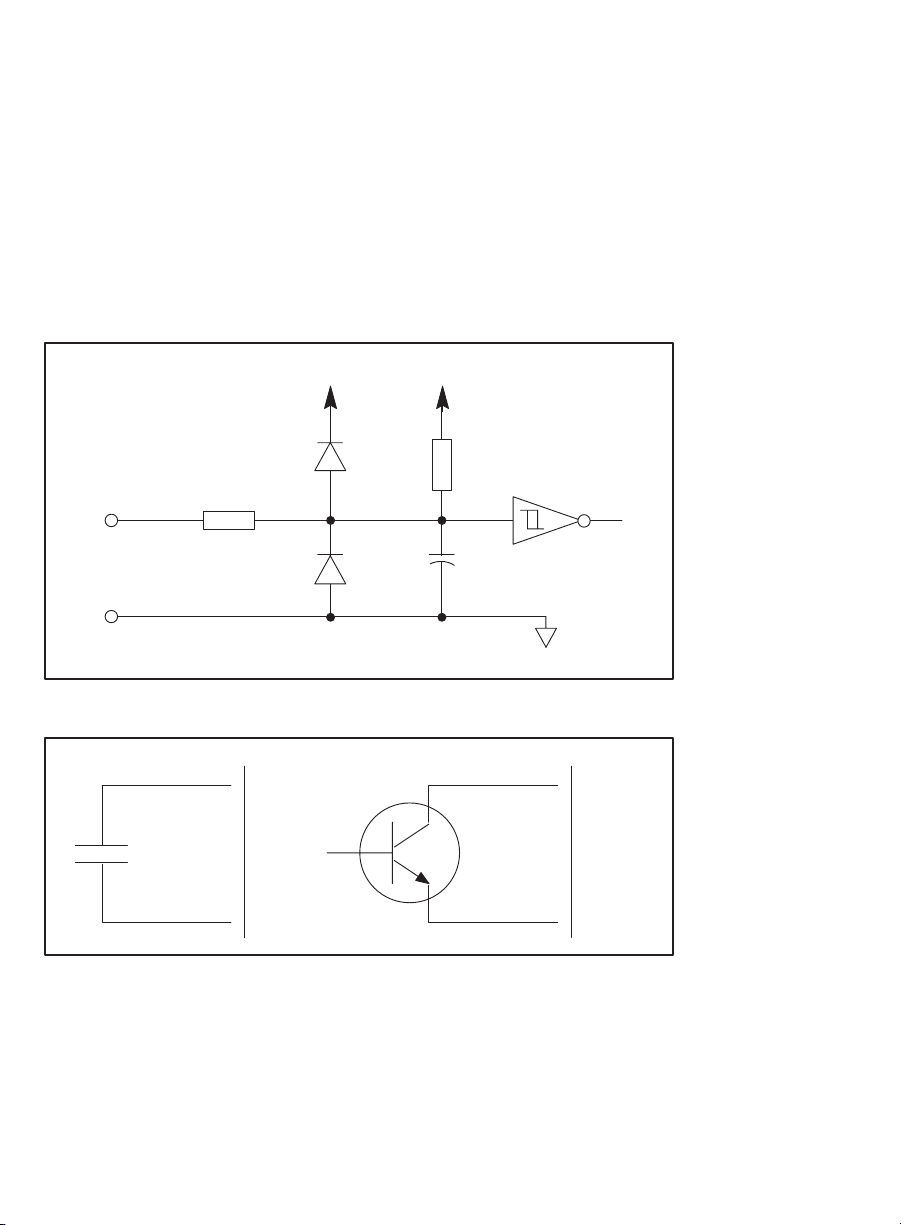
external event occurs. See figure 2.1 for details about the electrical
characteristics of the external strobe input circuit. Because of the high
input impedance of the strobe input, the device driving the input
must have low leakage. See figure 2.2.
The module can be programmed to generate an interrupt whenever it
does a periodic sample. This mode allows you to synchronize task
execution with the conversion of new data. The converted data will
be latched when the interrupt is generated.
The module contains a 2Ćbit electronic counter that can count a total
of 4 electrical resolver revolutions. This 2Ćbit counter is contained in
the most significant two bits of resolver position, registers 0 and 1.
This counter is reset whenever power is turned on to the system or a
board reset command occurs.
2Ć1
Page 10
The module produces a 26 volt rms 2381 Hertz sine wave reference
output signal which is capable of driving a 400 ohm load. This
reference signal is transformerĆisolated and shortĆcircuit protected
through a current limiter. The module also receives 11.8 volt rms sine
and cosine signals from the resolver, as well as the 26 volt rms
reference.
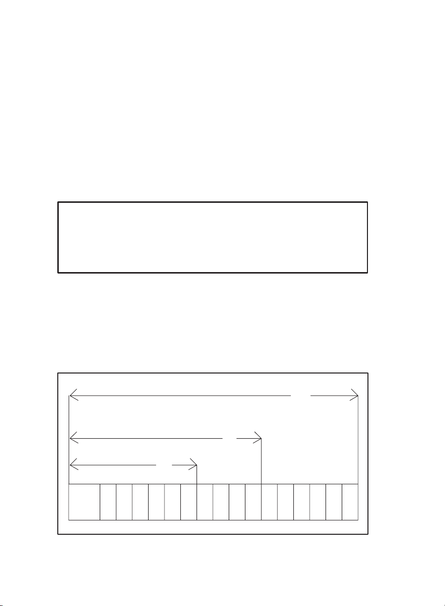
There are 5 LEDs on the faceplate of the module. The top LED,
labeled DIRECTION, indicates the direction of rotation of the resolver.
When it is on, the resolver is rotating clockwise. The next LED,
labeled FDBK OK, indicates that the resolver is connected to the
module. The next LED, labeled CCLK OK, indicates that the common
clock is on. The fourth LED, labeled IPS OK, indicates that the
isolated power supply is working. Finally, the bottom LED, labeled
OK, indicates whether the common clock is on and the isolated
power supply is functional. See figure 2.3.
+12V +12V
1
M
9
10
100k
2200 pf
40106
Figure 2.1 Ć External Strobe Input Circuit
9
10
Figure 2.2 Ć Low Leakage Requirement for Devices Driving Strobe Input
2Ć2
0V
9
10
Page 11
RESOLVER
INPUT
OK
DE
P3
C
B
1
2
3
4
5
6
7
8
9
1
0
3
2
1
F
G
6
7
8
Figure 2.3 Ć Module Faceplate
2Ć3
Page 12

Page 13
3.0 INSTALLATION
3.1 Wiring
The installation of wiring should conform to all applicable codes.
To reduce the possibility of electrical noise interfering with the proper
operation of the control system, exercise care when installing the
wiring from the system to the external devices. For detailed
recommendations, refer to IEEE 518.
You should use twisted pair (2 twists per inch) wiring to/from the
resolver.
3.2 Initial Installation
Use the following procedure to install the module:
WARNING
INSERTING OR REMOVING THIS MODULE OR ITS CONNECTING CABLES MAY
RESULT IN UNEXPECTED MACHINE MOTION. POWER TO THE MACHINE
SHOULD BE TURNED OFF BEFORE INSERTING OR REMOVING THE MODULE
OR ITS CONNECTING CABLES. FAILURE TO OBSERVE THESE PRECAUTIONS
COULD RESULT IN BODILY INJURY.
Step 1. Remove power from the system. Power to the rack as well
Step 2. Take the module out of its shipping container. Take the
Step 3. Insert the module into the desired slot in the rack. Refer to
Typical 16 Slot Rack
Typical 10 Slot Rack
Typical 6 Slot Rack
P/S
0123456789101112131415
as all power to the wiring leading to the module should be
off.
module out of the antiĆstatic bag. Be careful not to touch
the connectors on the back of the module.
figure 3.1. Use a screwdriver to secure the module into the
slot.
16
10
6
Figure 3.1 Ć Rack Slot Numbers
3Ć1
Page 14
Step 4. Mount the terminal strip (from cable assembly M/N
57C373) on a panel. The terminal strip should be mounted
to allow easy access to the screw terminals. Be sure that
the terminal strip is close enough to the rack so that the
cable will reach between the terminal strip and the
module. The cable assembly is approximately 60 inches
long.
Step 5. Attach the resolver but leave the mechanical coupling
between the resolver and the motor unconnected.
Fasten the field wires from the resolver to the terminal
strip. Typical field connections are shown in figures 3.2
and 3.3.
Use twistedĆpair wire, connected as shown, for the cabling
between the resolver and the terminal strip in the control
enclosure. Recommended twistedĆpair wire is Belden
9497 cable or equivalent. Maximum operating cable length
is dependent upon the type of cable you use.
Make certain that all field wires are securely fastened.
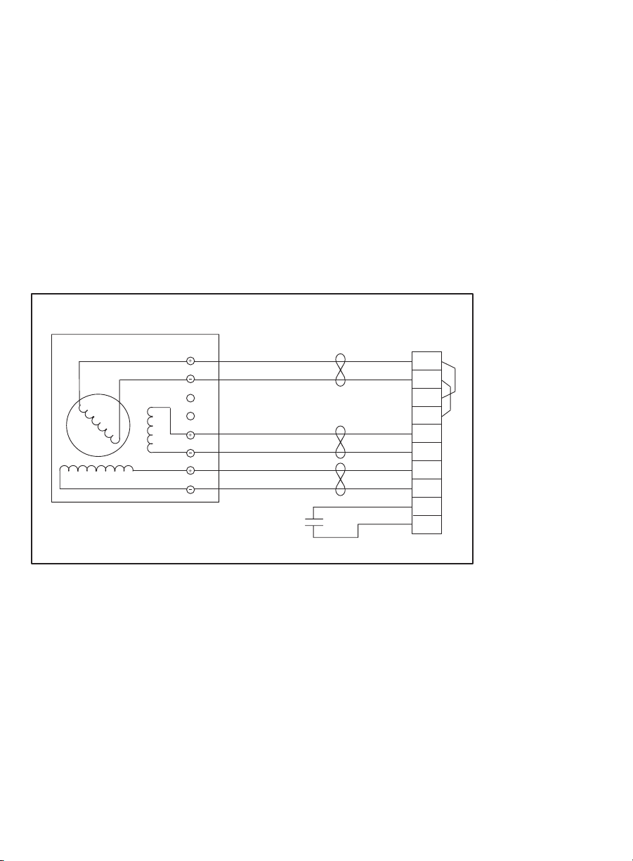
M/N 57C360 RESOLVER
REFERENCE
SINE
COSINE
REFERENCE VOLTAGE: 26 Vrms
SINE VOLTAGE: 11.8 Vrms
COSINE VOLTAGE: 11.8 Vrms
Figure 3.2 Ć Typical M/N 57C360 Resolver Field Connections
Terminal Strip
in Control
R1
FROM MODULE
R2
Enclosure
ă1
ă2
ă3
ă4
S1
TO MODULE
S3
S2
S4
ă5
ă6
ă7
ă8
ă9
10
3Ć2
Page 15

M/N 57C361 RESOLVER
REFERENCE
SINE
COSINE
REFERENCE VOLTAGE: 26 Vrms
SINE VOLTAGE: 11.8 Vrms
COSINE VOLTAGE: 11.8 Vrms
Figure 3.3 Ć Typical M/N 57C361 Resolver Field Connections
Terminal Strip
in Control
A
FROM MODULE
B
Enclosure
ă1
ă2
ă3
ă4
D
TO MODULE
F
G
E
ă5
ă6
ă7
ă8
ă9
10
Step 6. Insert the cable assembly's (M/N 57C373) field terminal
connector into the mating half on the module. Use a
screwdriver to secure the connector to the module.
Note that both the module and the terminal strip connector
are equipped with keys". These keys should be used to
prevent the wrong cable from being connected to the
module in the event that the connector needs to be
removed for any reason and then reattached later.
At the time of installation, rotate the keys on the module
and the connector so that they can be connected together
securely. It is recommended that, for modules so
equipped, the keys on each succeeding module in the
rack be rotated one posistion to the right of the keys on
the preceeding module.
If you use this method, the keys on a particular connector
will be positioned in such a way as to fit together only with
a specific module, and there will be little chance of the
wrong connector being attached to a module.
Step 7. Check the wiring and be sure all connections are tight.
Step 8. With the resolver mechanically disconnected from the
motor, turn on power to the rack. Use an oscilloscope to
test the sine and the cosine signals from the resolver.
These signals, measured at the terminal strip, should be a
sine wave of approximately 33.4 VpĆp (11.8 Vrms +/10%).
Step 9. Verify the installation by using the Programming Executive
Software. Refer to the AutoMax Programming Executive
Manual (JĆ3630 or JĆ3684) for more information.
Use the I/O MONITOR function for local I/O or remote I/O,
depending upon where the module is located. Set register
4 to a value of 1. Read register 2 and verify that bit 10 is
set. If it is not, set register 3 to a value of 64.
3Ć3
Page 16

Monitor register 0. Verify that it contains numbers
proportional to the shaft position of the resolver and that
the numbers increase as the resolver is rotated clockwise.
The direction of rotation can be reversed by switching the
polarity of either the sine or the cosine wires. See figure 3.4.
CLOCKWISE ROTATION = COUNT UP
SIN +
SINE
SIN -
COSINE
COS +
COS -
RESOLVER
57C411
CLOCKWISE ROTATION = COUNT DOWN
SIN +
SINE
COSINE
SIN -
COS +
COS -
RESOLVER
57C411
CLOCKWISE ROTATION = COUNT DOWN
SIN +
SINE
COSINE
SIN -
COS +
COS -
RESOLVER
57C411
NOTE 1: All wires should be twisted pairs.
NOTE 2: Reversing the polarity of the wires as shown will
also change the perceived shift angle by 180 elecĆ
trical degrees.
3Ć4
Figure 3.4 Ć Changing the Direction of Rotation
Step 10. If the external strobe input is being used, the shaft should
be rotated to a fixed position and stopped. The external
strobe input should now be closed. Verify that register 1
contains the same data as register 0.
Step 11. Turn off power to the rack. Connect the mechanical
coupling between the resolver and the motor. Turn on
power to the system.
Page 17

3.3 Module Replacement
WARNING
INSERTING OR REMOVING THIS MODULE OR ITS CONNECTING CABLES MAY
RESULT IN UNEXPECTED MACHINE MOTION. POWER TO THE MACHINE
SHOULD BE TURNED OFF BEFORE INSERTING OR REMOVING THE MODULE
OR ITS CONNECTING CABLES. FAILURE TO OBSERVE THESE PRECAUTIONS
COULD RESULT IN BODILY INJURY.
Use the following procedure to replace a module:
Step 1. Turn off power to the rack and all connections.
Step 2. Use a screwdriver to loosen the screws holding the
Step 3. Loosen the screws that hold the module in the rack.
Step 4. Place the module in the antiĆstatic bag, being careful not
Step 5. Take the new module out of the antiĆstatic bag it came in,
Step 6. Insert the module into the desired slot in the rack. Use a
Step 7. Attach the field terminal connector (M/N 57C373) to the
Step 8. Turn on power to the rack.
connector to the module. Remove the connector from the
module.
Remove the module from the slot in the rack.
to touch the connectors on the back of the module. Place
the module in the cardboard shipping container.
being careful not to touch the connectors on the back of
the module.
screwdriver to secure the module into the slot.
mating half on the module. Make certain that the
connector is the proper one for this module (see step 6 in
3.2 Initial Installation). Use a screwdriver to secure the
connector to the module.
3Ć5
Page 18

Page 19
4.0 PROGRAMMING
This section describes how the data is organized in the module and
provides examples of how the module is accessed by the application
software. For more detailed information refer to the DCS 5000
Enhanced BASIC Language Instruction Manual (JĆ3600).
4.1 Register Organization
The input module contains a total of five 16Ćbit registers. Registers 0
and 1 contain resolver position data. The resolverĆtoĆdigital converter
provides 12 bits of resolution. Register 0 is updated with new position
information at the rate specified in register 4. Register 1 is updated
whenever the EXTERNAL STROBE goes from false to true. These
registers are read only. Refer to figure 4.1.
register 0
register 1
bits
resolver data
resolver external latch data
electronic revolution counter
Figure 4.1 Ć Resolver Data Registers
Registers 2 and 3 are the interrupt status and control registers. Both
registers contain the same information. Register 2 is read only.
Register 3 is read/write. If the module is located in a remote rack, you
must read the status from register 2. With the exception of bit 6 and
bit 12, this register is controlled by the operating system and must
not be manipulated by the user. Refer to figure 4.2.
For this module to operate properly, the common clock signal must
be present on the backplane. The common clock signal isa4mhz
clock that can be connected to all the I/O modules in the rack. It can
be generated from a number of DCS 5000 I/O modules. If this
module is to drive the common clock, bit 6 must be set.
0123456789101112131415
00
00
4Ć1
Page 20

bits
register 2
register 3
0123456789101112131415
R RRRRRRR RR Ć Ć ĆRRR
RW R R RW R R R R RW RW Ć Ć Ć RW RW RW
bits
register 4
ăăă Interrupt allocated
Interrupt line ID
ăăăăInterrupt clock enable
ăăăăInterrupt enabled
Module fault
ăResolver not connectedă
ăăăăăCommon clock off
Isolated power fault
External strobe reset
Position angle increasing
External strobe status
Interrupt flag status
Figure 4.2 Ć Interrupt Control Registers
Register 4 contains the update period for reading the resolver
position. Each count in this register is equivalent to 500
microseconds. The update period may range from 500 microseconds
to 32.7675 seconds. Refer to figure 4.3.
0123456789101112131415
update period
Figure 4.3 Ć Resolver Update Register
4.2 Local I/O Definition
Before any application program can be written, it is necessary to
configure, or set, the definitions of systemĆwide variables, i.e. those
that must be globally accessible to all tasks. This section describes
how to configure the input module when it is located in the same rack
as the processor module that is referencing it. Refer to figure 4.4.
4Ć2
Page 21

Processor Module
POWER
SUPPLY
120V
LINK
GND
275 W
RESOLVER
INPUT
57C411
0
0
POWER ON
P S READY
SYSTEM READY
BLOWN FUSE
NORMAL
DE
F
C
B
G
L2
L1
3
6
2
7
1
8
FUSE
BATTERY
BACKĆUP
57491
OK
REMOTEPROGRAM
1
2
3
4
5
6
7
OK
8
9
10
11
12
13
14
DE
15
F
C
B
G
0
1
2
3
C1
4
5
P3
DE
6
F
C
B
G
7
C2
8
9
10
11
C3
12
13
14
15
C4
6
6
3
3
7
7
2
2
1
8
1
8
0
1
1
2
2
3
3
4
4
5
5
6
6
7
7
8
8
9
9
10
10
11
11
12
12
13
13
14
14
DE
15
C1
C2
10
11
C3
12
13
14
15
C4
DE
15
F
F
C
C
B
G
B
0
1
2
3
4
5
6
7
8
9
G
0
1
2
3
C1
4
5
6
7
C2
8
9
10
11
C3
12
13
14
15
C4
6
6
3
3
7
7
2
2
1
8
1
8
0
0
1
2
3
4
5
6
7
8
9
10
11
12
13
14
DE
15
F
C
B
G
0
1
2
3
C1
4
5
6
7
C2
8
9
10
11
C3
12
13
14
15
C4
6
3
7
2
1
8
0
1
1
2
2
3
3
4
4
5
5
6
6
7
7
8
8
9
9
10
10
11
11
12
12
13
13
14
14
DE
15
C1
C2
10
11
C3
12
13
14
15
C4
DE
15
F
C
B
0
1
2
3
4
5
6
7
8
9
3
2
F
C
G
B
G
0
1
2
3
C1
4
5
6
7
C2
8
9
10
11
C3
12
13
14
15
C4
6
6
3
7
7
2
1
8
1
8
Module
Figure 4.4 Ć Module in a Local Rack
4.2.1 Single Register Reference
Use this method to reference a 16Ćbit register as a single input.
Resolver input data, update period, and interrupt control registers are
typically referenced using this method. The symbolic name of each
register should be as meaningful as possible:
nnnnn IODEF SYMBOLIC_NAME%[ SLOT=s, REGISTER=r]
4.2.2 Bit Reference
Use this method to reference individual inputs on the module.
Common clock status and control bits are typically referenced using
this method. The symbolic name of each bit should be as meaningful
as possible:
nnnnn IODEF SYMBOLIC_NAME@[ SLOT=s, REGISTER=r, BIT=b]
where:
nnnnn Ć BASIC statement number. This number may range from
1Ć32767.
4Ć3
Page 22

SYMBOLIC_NAME% Ć A symbolic name chosen by the user and
ending with (%). This indicates an integer data type and all
references will access register r".
SYMBOLIC_NAME@ Ć A symbolic name chosen by the user and
ending with (@). This indicates a boolean data type and all
references will access bit number b" in register r".
SLOT Ć Slot number that the module is plugged into. This number
may range from 0Ć15.
REGISTER Ć Specifies the register that is being referenced. This
number may range from 0Ć4.
BIT Ć Used with Boolean data types only. Specifies the bit in the
register that is being referenced. This number may range from 0Ć 15.
4.2.3 Examples of Local I/O Definitions
The following statement assigns the symbolic name POSITION% to
register 0 of the input module located in slot 4:
1020ăăIODEF POSITION%[ SLOT=4, REGISTER=0]
The following statement assigns the symbolic name CCLK_ON@ to
bit 6 of register 3 on the input module located in slot 7:
2050ăăIODEF CCLK_ON@[ SLOT=7, REGISTER=3, BIT=6]
4.3 Remote I/O Definition
This section describes how to configure the module when it is
located in a rack that is remote from the processor module
referencing it. Refer to figure 4.5.
4Ć4
Page 23

Drop 0
Remote I/O Master
Processor Module
I/O Module
Master Rack
Remote I/O Slave
Drop 7
Remote I/O Slave
Drop 2
Figure 4.5 Ć Module in a Remote Rack
4.3.1 Single Register Reference
Use this method to reference a 16Ćbit register as a single input.
Resolver input data and update period registers are typically
referenced using this method. The symbolic name of each register
should be as meaningful as possible:
nnnnnăăRIODEF SYMBOLIC_NAME%[ MASTER_SLOT=m,
ăăăăDROP=d, SLOT=s, REGISTER=r]
Remote I/O Slave
Drop 1
4Ć5
Page 24

4.3.2 Bit Reference
Use this method to reference individual inputs on the module.
Common clock status and control bits are typically referenced using
this method. The symbolic name of each bit should be as meaningful
as possible:
nnnnnăăRIODEF SYMBOLIC_NAME@[ MASTER_SLOT=m,
ăăăăDROP=d, SLOT=s, REGISTER=r, BIT=b]
where:
nnnnn Ć BASIC statement number. This number may range from
1Ć32767.
SYMBOLIC_NAME% Ć A symbolic name chosen by the user and
ending with (%). This indicates an integer data type and all
references will access register r".
SYMBOLIC_NAME@ Ć A symbolic name chosen by the user and
ending with (@). This indicates a boolean data type and all
references will access bit number b" in register r".
MASTER_SLOT Ć Slot number that the master remote I/O module is
plugged into. This number may range from 0Ć15.
DROP Ć Drop number of the slave remote I/O module that is in the
same rack as the input module. This number may range from 1Ć7.
SLOT Ć Slot number that the module is plugged into. This number
may range from 0Ć15.
REGISTER Ć Specifies the register that is being referenced. This
number may range from 0Ć4.
BIT Ć Used with boolean data types only. Specifies the bit in the
register that is being referenced. This number may range from 0Ć15.
4.3.3 Examples of Remote I/O Definitions
The following statement assigns the symbolic name SHAFT% to
register 0 on the input module located in slot 4 of remote I/O drop 3.
This remote drop is connected to the remote I/O system whose
master is located in slot 15 in the master rack:
1020ăăRIODEF SHAFT%[ MASTER_SLOT=15, DROP=3,
ăăăSLOT=4, REGISTER=0]
The following statement assigns the symbolic name CLCK_EN@ to
bit 6 of register 3 on the input module located in slot 7 of remote I/O
drop 2. This remote drop is connected to the remote I/O system
whose master is located in slot 6 in the master rack:
2050ăăRIODEF CLCK_EN@[ MASTER_SLOT=6,
ăăăDROP=2, SLOT=7, REGISTER=3, BIT=6]
4.4 Reading and Writing Data in Application Tasks
In order for an input module to be referenced by application
software, it is first necessary to assign symbolic names to the
physical hardware. This is accomplished with either IODEF or
RIODEF statements in the configuration task.
4Ć6
Page 25

Each application program, or task, that wishes to reference the
symbolic names assigned to the input module may do so by
declaring those names COMMON.
The frequency with which tasks read their inputs and write their
outputs depends on the language being used. Control block tasks
read inputs once at the beginning of each scan and write outputs
once at the end of scan. BASIC tasks read an input and write an
output for each reference throughout the scan.
The following is an example of a configuration task for the input
module:
1000 !
1001 ! resolver input
1002 !
1005 IODEF RESOLVER_IN%[SLOT=4, REGISTER=0]
1006 IODEF RESOLVER_IN_EXT%[SLOT=4, REGISTER=1]
1010 !
1011 ! common clock enable
1012 !
1015 IODEF CCLK_EN@[SLOT=4, REGISTER=3, BIT=6]
1020 !
1021 ! A/D update period
1022 !
1025 IODEF UPDATE_TIME%[SLOT=4, REGISTER=4]
1050 !
1051 ! Place any additional configurationăstatements here
1052 !
2000 END
4.4.1 BASIC Task Example
This example will read the resolver input once every second and
store the value in the symbol CURRENT_VALUE". The resolver
position will be sampled every 100 milliseconds.
1000 COMMON RESOLVER_IN% \!Resolver data(periodic)
1010 COMMON CCLK_EN@ \!common clock enable
1020 COMMON UPDATE_TIME% \!Update period for resolver conversion
1400 !
1500 LOCAL CURRENT_VALUE% \!Current value of analog input
1900 !
2000 UPDATE_TIME% = 200 \!0.1 second conversion
2010 CCLK_EN@ = TRUE \!turn on the clock
4000 !
4001 ! Place any additional initialization software here
4002 !
5000 START EVERY 1 SECONDS
5010 CURRENT_VALUE% = RESOLVER_IN%
10000 END
The symbolic names defined as COMMON" reference the inputs
defined in the sample configuration task above. The symbolic name
CURRENT_VALUE% is local to the BASIC task and does not have I/O
associated with it. Refer to the DCS 5000 Enhanced BASIC
Language Instruction Manual (JĆ3600) for more information.
4.4.2 Control Block Task Example
The following example will read the resolver data every 55
milliseconds and store the inverted value in the symbol READING".
The resolver's shaft position will be sampled every 500
microseconds.
1000 COMMON RESOLVER_IN% \!Resolver data (periodic)
1010 COMMON CCLK_EN@ \!Common clock enable
1020 COMMON UPDATE_TIME% \!Update period forĂresolver conv.
1400 !
1500 LOCAL READING% \!Current negative value of input
1600 !
4Ć7
Page 26

2000 UPDATE_TIME% = 1 \!500 microsecond conversion
2010 CCLK_EN@ = TRUE \!Turn on the clock
4000 !
4001 ! Place any additional initialization software here
4002 !
4998 ! Scan every 55 msec.
4999 !
5000 CALL SCAN_LOOP( TICKS=10)
5010 CALL INVERTER( INPUT= RESOLVER_IN%,OUTPUT=READING%)
10000 END
The symbolic names defined as COMMON" reference the inputs
defined in the sample configuration task above. The symbolic name
READING%" is local to the BASIC task and does not have I/O
associated with it. Refer to the DCS 5000 Control Block Language
Instruction Manual (JĆ3601) for more information.
4.5 Using Interrupts in Application Tasks
The input module supports an interrupt on the periodic
resolverĆtoĆdigital conversion. Interrupts are used to synchronize
software tasks with the resolverĆtoĆdigital conversion. Conversion
rates may be specified from 500 microseconds up to a maximum of
32.7675 seconds in increments of 500 microseconds.
In order to use interrupts on the input module, it is necessary to
assign symbolic names to the interrupt control register. This is
accomplished with IODEF statements in the configuration task. Note
that interrupts cannot be used with modules located in remote racks.
Only one task may act as a receiver for a particular hardware
interrupt. That task should declare the symbolic names assigned to
the interrupt control register on the input module as COMMON. Once
this has been done, any reference to those symbolic names within
the task will reference the bits or register defined in the configuration
task.
The following is an example of a configuration task for an input
module using interrupts:
1000 !
1001 ! resolver data
1002 !
1005 IODEF RESOLVER_IN%[SLOT=4, REGISTER=0]
1006 IODEF RESOLVER_IN_EXT%[SLOT=4, REGISTER=1]
1010 !
1011 ! interrupt status and control register (used by the operating system)
1012 !
1014 IODEF STROBE_STATUS@( SLOT=4, REGISTER=2,BIT=14)
1015 IODEF ISCR%[SLOT=4, REGISTER=3]
1016 IODEF STROBE_ACK@( SLOT=4, REGISTER=3,BIT=12)
1020 !
1021 ! common clock enable
1022 !
1025 IODEF CCLK_EN@[SLOT=4, REGISTER=3, BIT=6]
1030 !
1031 ! resolver conversion period
1032 !
1035 IODEF UPDATE_TIME%[SLOT=4, REGISTER=4]
1050 !
1051 ! Place additional configuration statements here
1052 !
2000 END
This configuration defines all of the information most commonly used
on the module. Unused definitions should be deleted by the user.
4Ć8
Page 27

4.5.1 BASIC Task Example
The following is an example of a BASIC task that handles interrupts
from the input module defined in section 4.4.
1000 COMMON RESOLVER_IN% \!Resolver data
1005 COMMON ISCR% \!Interrupt status & control
1010 COMMON CCLK_EN@ \!Common clock enable
1020 COMMON UPDATE_TIME% \!Resolver conversion time
1200 LOCAL RESOLVER_VALUE% \!Resolver value
2000 !
2001 ! Define the conversion parameters
2002 !
2010 UPDATE_TIME% = 1000 \!Convert every .5 seconds
3000 !
3001 ! The following statement connects the name RESOLVER_EVENT to the
3002 ! interrupt defined in ISCR%. The event name chosen should
3003 ! be as meaningful as possible. The watchdog timeout has
3004 ! been set to 120 clock ticks (660 msec). If the time between
3005 ! interrupts exceeds this value, a severe error will be declared
3006 ! and the system will be stopped. For more information refer to the
3007 ! DCS 5000 Enhanced BASIC Language Instruction Manual (JĆ3600).
3008 !
3010 EVENT NAME=RESOLVER_EVENT,
3011 ăăINTERRUPT_STATUS=ISCR%,TIMEOUT=120
4000 !
4001 ! The following statement enables common clock from this module
4002 ! If there is more than one interrupt task in a chassis, the task
4003 ! that enables common clock should always be the lowest priority
4004 ! task.
4005 !
4010 CCLK_EN@ = TRUE \!Common clock enable
5000 !
5001 ! Place additional initialization software here
5002 !
6000 !
6001 ! The next statement synchronizes the task with the external
6002 ! event via the interrupt. Task execution will be suspended
6003 ! until the interrupt occurs. If this task is the highest
6004 ! priority task waiting to execute at the time of the
6005 ! interrupt, it will become active. If it is not the
6006 ! highest priority task, it will remain suspended until
6007 ! all higher priority tasks have executed, at which point
6008 ! it will become active.
6009 !
6010 WAIT ON RESOLVER_EVENT
7000 !
7001 ! The next statements perform the interrupt service routine
7002 !
7010 RESOLVER_VALUE% = RESOLVER_IN%
10000 END
4.5.2 Control Block Task Example
The following is an example of a control block task that handles
interrupts from the input module defined in section 4.4.
1000 COMMON RESOLVER_IN% \!Resolver data
1005 COMMON ISCR% \!Interrupt status & control
1010 COMMON CCLK_EN@ \!Common clock enable
1020 COMMON UPDATE_TIME% \!Resolver conversion time
1200 LOCAL RESOLVER_VALUE% \!Resolver value
2000 !
2001 ! Define the conversion parameters
2002 !
2010 UPDATE_TIME% = 100 \!Convert every 50 milliĆseconds
3000 !
3001 ! The following statement connects the name RESOLVER_EVENT to
3002 ! the interrupt defined in ISCR%. The event name chosen should
3003 ! be as meaningful as possible. The watchdog timeout has
3004 ! been set to 12 clock ticks (66 msec). If the time between
3005 ! interrupts exceeds this value, a severe error will be declared
3006 ! and the system will be stopped. For more information refer to the
3007 ! DCS 5000 Enhanced BASIC Language Instruction Manual (JĆ3600).
3008 !
3010 EVENT NAME=RESOLVER_EVENT, &
3011 ăăINTERRUPT_STATUS=ISCR%, TIMEOUT=12
4Ć9
Page 28

4000 !
4001 ! The following statement enables common clock from this module.
4002 ! If there is more than one interrupt task in a chassis, the task
4003 ! that enables common clock should always be the lowest priority
4004 ! task.
4005 !
4010 CCLK_EN@ = TRUE \!Common clock enable
5000 !
5001 ! Place additional initialization software here
5002 !
6000 !
6001 ! The next statement synchronizes the task with the external
6002 ! event via the interrupt. Task execution will be suspended
6003 ! until the interrupt occurs. If this task is the highest
6004 ! priority task waiting to execute at the time of the
6005 ! interrupt, it will become active. If it is not the
6006 ! highest priority task, it will remain suspended until
6007 ! all higher priority tasks have executed, at which point
6008 ! it will become active.
6009 !
6010 CALL SCAN_LOOP(TICKS=9, EVENT=RESOLVER_EVENT)
7000 !
7001 ! The next statements perform the interrupt service routine
7002 !
7010 CALL PULSE_MULT(INPUT= RESOLVER_IN%, MULTIPLIER=16385, &
10000 END
OUTPUT= RESOLVER_VALUE%)
4.6 Using the External Strobe Input
At the time of the external event, the resolver position is transferred to
register 1, where it will remain until the next event occurs. If your
application software is reading the resolver position at a periodic rate
(register 0), the difference between register 0 and register 1
represents the amount of travel from the time that the event occurred
until the current scan of the application software. A typical application
would be detecting the leading edge of an object moving on a
conveyor.
The data captured by the strobe input will be as accurate as the
external device driving the input. Note that when a strobe input has
occurred, you must reset the input so that another one can occur.
This is accomplished by writing a 1" to bit 12 of register 3.
The following is an example of a control block task that handles the
strobe input from the input module defined in section 4.4.
1000 COMMON RESOLVER_IN% \!Resolver data
1001 COMMON RESOLVER_IN_EXT% \!Strobe resolver data
1005 COMMON ISCR% \!Interrupt statusă& control
1010 COMMON CCLK_EN@ \!Common clock enable
1020 COMMON UPDATE_TIME% \!Resolver conversion time
1030 COMMON STROBE_STATUS@ \!Strobe status
1040 COMMON STROBE_ACK@ \!Strobe acknowledge
1200 LOCAL RESOLVER_VALUE% \!Resolver value
1210 LOCAL STROBE_RESET@ \!Strobe state
1220 LOCAL PERIOD_DISTANCE% \!Resolver travel scan/scan
1230 LOCAL EVENT_DISTANCE% \!Resolver travel from event to scan
2000 !
2001 ! Define the conversion parameters
2002 !
2010 UPDATE_TIME% = 100 \!Convert every 50 milliseconds
3010 EVENT NAME=RESOLVER_EVENT,INTERRUPT_STATUS=ISCR%, &
ąąTIMEOUT=12
4010 CCLK_EN@ = TRUE \!Common clock enable
6008 !
6010 CALL SCAN_LOOP( TICKS=9, EVENT=RESOLVER_EVENT)
7000 !
7001 ! The next statements catch the occurence
7002 ! of the strobe and reset it.
7003 !
7010 CALL TRANSITION ( INPUT= STROBE_STATUS @, &
7020 STROBE_ACK@= NOT STROBE_RESET@
OUTPUT=STROBE_RESET@)
4Ć10
Page 29

7025 !
7026 ! The next statement calculates the distance
7027 ! traveled from the occurrence of the external
7028 ! event until this scan.
7029 !
7030 CALL PULSE_MULT( INPUT=RESOLVER_IN%,ăăăă&
7036 ! The next statement calculates the distance traveled
7037 ! from the last scan until this scan.
7039 !
7040 CALL PULSE_MULT( INPUT=RESOLVER_IN%, &
7046 !
7047 ! The next statement calculates the correction
7048 ! required to synchronize the external event to
7049 ! the program.
7050 !
7060 CALL DIFFERENCE( INPUT1=PERIOD_ DISTANCE%, &
10000 END
RESET=-STROBE_RESET@,ăă&
INITIAL_VALUE =RESOLVER_IN_EXT%, &
MULTIPLIER=16385,ăăăăăăăăă&
OUTPUT=EVENT_DISTANCE%)
MULTIPLIER=16385, &
OUTPUT=PERIOD_DISTANCE%)
INPUT2=EVENT_DISTANCE%, &
OUTPUT=RESOLVER_VALUE%)
4.7 Restrictions
This section describes limitations and restrictions on the use of this
module.
4.7.1 Writing Data to Registers
Registers 0Ć2 are read only and may not be written to by the
application software. Attempts to write to them will cause a bus error
(severe system error). The following are examples from programs
that write to the module and should therefore be avoided:
a. Referencing the module on the left side of an equal sign in a LET
statement in a control block or BASIC task.
b. Referencing a resolver input as an output in a control block
function.
4.7.2 Interrupts in Remote I/O Racks
This module cannot be used in the interrupt mode in a remote rack.
4.7.3 Feedback Element in a Drive System
When this module is used with a resolver in a drive control system,
you must incorporate an independent method of determining that
this module is actually reading proper motor RPM. It is necessary to
determine this because this module is not capable of detecting a loss
of feedback in all situations, such as, for example, a broken coupling
between the motor and resolver.
4Ć11
Page 30

WARNING
LOSS OF, OR OTHERWISE IMPROPER, RESOLVER SIGNAL CAN RESULT IN
UNCONTROLLED MOTOR SPEED. PROVIDE AN INDEPENDENT METHOD OF
SHUTTING DOWNEQUIPMENT IFTHIS SHOULDOCCUR. FAILURE TO OBSERVE
THIS PRECAUTION COULD RESULT IN BODILY INJURY AND IN DAMAGE TO,OR
DESTRUCTION OF, THE EQUIPMENT.
You must also determine the maximum safe operating speed for the
motor, connected machinery, and material being processed. Then,
either verify that the system is incapable of reaching that speed, or
else incorporate the necessary hardware/software to ensure that this
limit will never be exceeded.
WARNING
THE PURCHASER IS RESPONSIBLE FOR ENSURING THAT DRIVEN
MACHINERY, ALL DRIVE TRAIN MECHANISMS, AND THE WORKPIECE IN THE
MACHINE ARE CAPABLE OF SAFE OPERATION ATMAXIMUM SPEEDS. FAILURE
TO OBSERVE THESE PRECAUTIONS COULD RESULT IN BODILY INJURY AND IN
DAMAGE TO, OR DESTRUCTION OF, THE EQUIPMENT.
4Ć12
Page 31

5.0 DIAGNOSTICS AND TROUBLESHOOTING
This section explains how to troubleshoot the module and field
connections.
5.1 Incorrect Data
Problem: The data is either always off, always on, or different than
expected. The possible causes of this error are a module in the
wrong slot, a programming error, or a malfunctioning module. It is
also possible that the input is either not wired or wired to the wrong
device. Use the following procedure to isolate the problem:
Step 1. Verify that the input module is in the correct slot and that
Step 2. Verify that the module can be accessed.
Step 3. Verify that the user application program is correct.
Step 4. Verify that the resolver is wired correctly.
the I/O definitions are correct.
Refer to figure 3.1. Verify that the slot number being
referenced agrees with the slot number defined in the
configuration task. Verify that the register number and the
bit number are correct.
For remote I/O installations, also verify that the master slot
and drop numbers are defined correctly. Refer to the DCS
5000 Remote I/O Instruction Manual (JĆ3629) for more
detailed information on configuring your remote I/O
system.
Connect the programming terminal to the system and run
the ReSource Software. Use the I/O MONITOR function to
display the four registers on the input module. Repeat
steps 7 and 8 in section 3.2.
Review the programming examples in sections 4.4, 4.5,
and 4.6. Make certain that the I/O definitions in your
configuration task are correct and that the task(s) using
this module have declared these variables COMMON.
Verify that an update period has been written to register 4.
Recall that each count is 500 microseconds (.0005
seconds). This value specifies the frequency with which
the resolver position will be converted to digital numbers.
Verify that the common clock has been turned on. The
CCLK OK" LED on the faceplate of the module should be
lit. If the common clock is not present on the backplane,
the module will not convert the resolver position to digital
values. If the common clock is being generated from this
module, remember that bit 6 in register 3 must be set.
Remove power from the system. Disconnect the
mechanical coupling between the resolver and the motor.
Confirm that all the terminal strip connections are tight.
Refer to figures 3.2 and 3.3. Appendix C also lists the
terminal strip connections.
Apply power to the rack only.
5Ć1
Page 32

If everything is working properly but the direction of
rotation is backwards, it may be reversed by switching the
polarity of either the sine or the cosine wires as shown in
figure 3.4.
Step 5. Verify that the input circuit is working properly.
Connect an oscilloscope to the proper points on the
terminal strip and confirm that the voltages are correct.
The resolver reference voltage across TB 1 and 2 should
be a nominal 26 Vrms.
If it is 26 Vrms, check the jumpers on the terminal strip.
One jumper should connect TB 1 and 3. Another jumper
should connect TB 2 and 4. Rotate the resolver's shaft and
measure the sine voltage (TB 5 and 6) and cosine voltage
(TB 7 and 8). Both voltages should range from 0 volts to
approximately 11.8 Vrms.
If the resolver reference (TB 1 and 2) is not a nominal 26
Vrms, measure the DĆC resistance of the resolver.
Disconnect the resolver cable from the terminal strip (TB 1
and 2) and measure the resistance across the
disconnected wires.
The resistance should be in the range of 35 to 125 ohms.
If the resistance is within this range, the input module is
malfunctioning and should be replaced. If the resistance is
not within this range, disconnect the cabling from the
resolver and measure the resistance directly on the
resolver.
If this resistance is reading within the 35 to 100 ohm
range, the resolver is operating properly. Check the
cabling for a possible short. If the resistance is not within
the 35 to 100 ohm range, the resolver is malfunctioning
and should be replaced. If the problem is still present,
check the cable for a possible short.
Reconnect the resolver cable at TB 1 and 2.
Remove power from the rack. Reconnect the mechanical
coupling between the resolver and the motor. Reapply
power to the system.
Step 6. Verify that the hardware is working properly.
WARNING
INSERTING OR REMOVING THIS MODULE OR ITS CONNECTING CABLES
MAY RESULT IN UNEXPECTED MACHINE MOTION. POWER TO THE
MACHINE SHOULD BE TURNED OFF BEFORE INSERTING OR REMOVING
THE MODULE OR ITS CONNECTINGCABLES. FAILURE TO OBSERVE THESE
PRECAUTIONS COULD RESULT IN BODILY INJURY.
If all of the proper signals are present and the values are
still not correct, the problem lies in the hardware. Verify the
hardware functionality by systematically swapping out
modules. After each swap, if the problem is not corrected,
replace the original item before swapping out the next
item.
5Ć2
Page 33

To test local I/O, first replace the input module. Next,
replace the processor module (s). If the problem persists,
take all of the modules except one processor module and
the input module out of the backplane. If the problem is
now corrected, one of the other modules in the rack is
malfunctioning. Reconnect the other modules one at a
time until the problem reappears. If none of these tests
reveals the problem, replace the backplane.
To test remote I/O, first verify that the remote I/O system is
communicating with the drop that contains the input
module being tested. Next, by systematically swapping
out modules, determine whether the input module is the
only module that is not working.
If more than one module is not working correctly, the
problem most likely lies in the remote I/O system. Refer to
the the DCS 5000 Remote I/O Instruction Manual (JĆ3629)
for additional information. If the problem does not lie in the
system, it probably involves the remote rack.
To test the remote rack, first replace the input module. If
the problem persists, take all of the modules out of the
remote backplane except the slave remote I/O module
and the input module. If the problem is now corrected,
one of the other modules in the rack is malfunctioning.
Reconnect the other modules one at a time until the
problem reappears. If the problem proves to be neither in
the remote I/O system nor in the remote rack, try replacing
the backplane.
Problem: A 31" or 16" appears on the processor module's LED.
This error message indicates that there was a bus error when the
system attempted to access the module. The possible causes of this
error are a missing module, a module in the wrong slot, or a
malfunctioning module. It is also possible that the user has attempted
to write to the wrong registers on the module. Use the following
procedure to isolate a bus error:
Step 1. Verify that the input module is in the correct slot and that
Step 2. Verify that the module can be accessed.
the I/O definitions are correct.
Refer to figure 3.2. Verify that the slot number being
referenced agrees with the slot number defined in the
configuration task. Verify that the register number is in the
range of 0Ć4.
For remote I/O installations, also verify that the master slot
and remote drop number are defined correctly.
Refer to the DCS 5000 Remote I/O Instruction Manual
(JĆ3629) for more information on configuring your remote
I/O system.
Connect the programming terminal to the system and run
the ReSource Software. Use the I/O MONITOR function to
display the four registers on the input module. If the
programmer is able to monitor the inputs, the problem lies
in the application software (refer to step 3). If the
5Ć3
Page 34

programmer cannot monitor the inputs, the problem lies in
the hardware (refer to step 4).
Step 3. Verify that the user application program is correct.
Registers 0 through 2 of the input module cannot be
written to. If a BASIC task caused the bus error, the error
log will contain the statement number in the task where
the error occurred. If a control block task caused the error,
you will need to search the task for any instances where
you wrote to an input.
Step 4. Verify that the hardware is working correctly.
Verify the hardware functionality by systematically
swapping out modules. After each swap, if the problem is
not corrected, replace the original item before swapping
out the next item.
To test local I/O, replace the input module, the processor
modules (s), and finally the backplane.
For remote I/O, determine whether the input module is the
only module that is not working. If it is not, the problem
most likely lies in the remote I/O system. Refer to the DCS
5000 Remote I/O Instruction Manual (JĆ3629) for additional
information. If the problem does not lie in the remote I/O
system, it probably involves the remote rack.
To test the remote rack, systematically swap out the input
module, the slave remote I/O module, and finally the
backplane. After each swap, if the problem is not
corrected, replace the original item before going on to the
next swap. If none of these actions correct the problem,
troubleshoot the remote I/O system.
5.3 Interrupt Problems
Problem: No interrupts at all or too many (unexpected) interrupts,
signified by error codes on the screen. Note that this module must be
in the same rack as the processor module that is to receive the
interrupts. Go through the following steps first before going on to the
more specific troubleshooting steps.
Step 1. Verify that the input module is in the correct slot and that
Step 2. Verify that the user application program is correct.
5Ć4
the I/O definitions are correct.
Refer to figure 3.2. Verify that the slot number being
referenced agrees with the slot number defined in the
configuration task.
Verify that the configuration task contains the proper
interrupt control definitions. Refer to the example in
section 4.6.
Verify that the application program that uses the symbolic
names defined in the configuration task has defined those
names as COMMON.
Compare your interrupt task with the examples given in
sections 4.5.1 and 4.5.2. Make certain that the actions
shown in the examples are performed in the same order in
your task.
Page 35

5.3.1 No Interrupts
Problem: The program does not execute, but no error codes are
displayed on the processor module faceplate. If interrupts are never
received by the application program and the timeout parameter in
the event definition was disabled, the task will never execute.
The watchdog timer for this module should never be disabled. Before
you can determine why the program did not execute, you must first
set the timeout parameter in the event definition. Run the program
again and proceed to section 5.3.2.
5.3.2 Hardware Event TimeĆOut
Problem: All tasks in the chassis are stopped and error code 12"
appears on the faceplate of the processor module. The interrupt has
either never occurred or is occurring at a slower frequency than the
value specified in the timeout parameter in the event definition. Use
the following procedure to isolate the problem.
Step 1. Verify that the timeout value is set correctly.
Check the value specified in the timeout parameter in the
event definition. The unit is in ticks. Each tick is equal to
5.5 msec. The timeout value should be at least 2 ticks
greater than the interrupt frequency. It can reasonably
range up to 1.5 times the interrupt frequency.
Step 2. Verify that the user application program is correct.
Review the examples in section 4.5. Make certain that
common clock has been enabled.
Step 3. Verify that the hardware is working correctly.
Systematically swap out the input module, the processor
module (s), and the backplane. After each swap, if the
problem is not corrected, replace the original item before
swapping out the next item.
5.3.3 Hardware Event Count Limit Exceeded
Problem: All tasks in the chassis are stopped and error code 1b"
appears on the faceplate of the processor module. A hardware
interrupt has occurred but no task is waiting. Use the following
procedure to isolate the problem:
Step 1. Verify that the user application program is correct.
Verify that your interrupt response task contains either a
WAIT ON event" or CALL SCAN_LOOP" statement that
will be executed. Check carefully to determine whether a
higher priority task is preventing the interrupt response
task from running. Make certain that the ordering of your
statements agrees with the examples in section 4.5.
Step 2. Verify that the hardware is working correctly.
Verify the hardware functionality by systematically
swapping out the input module, the processor module (s),
and the backplane. After each swap, if the problem is not
corrected, replace the original item before swapping out
the next item.
5Ć5
Page 36

5.3.4 Illegal Interrupt Detected
Problem: All tasks in the chassis are stopped and error code 1F"
appears on the faceplate of the processor module. A hardware
interrupt has occurred but no event has been defined.
Step 1. Verify that the user application program is correct.
Verify that your interrupt response task contains an
EVENT" statement that will be executed. Check carefully
to determine whether a higher priority task is preventing
the interrupt response task from running. Make certain
that the ordering of your statements agrees with the
examples in section 4.5.
Step 2. Verify that the hardware is working correctly.
Verify the hardware functionality by systematically
swapping out the input module, the processor module (s),
and the backplane. After each swap, if the problem is not
corrected, replace the original item before swapping out
the next item.
5Ć6
Page 37

Appendix A
Technical Specifications
Ambient Conditions
D Storage temperature: -40_ CĆ85_ C
D Operating temperature: 0_ CĆ60_ C
D Humidity: 5Ć90% nonĆcondensing
Maximum Module Power Dissipation
D 10 Watts
Dimensions
D Height: 11.75 inches
D Width: 1.25 inches
D Depth: 7.375 inches
System Power Requirements
D 5 Volts: 1700 ma
D +12 Volts: 95 ma
D -12 Volts: 95 ma
Resolver Specifications
D Frequency of operation: 2381 Hz
D Minimum rotor impedance: 400 Ohms
D Transformer ratio: 26/11.8
External Strobe Minimum Trigger Time
D 1 millisecond
AĆ1
Page 38

Page 39

Appendix B
Module Block Diagram
BUS
ADDRESS
ID BUS
ADDRESS
BUS
CONTROL
LINES
CCLK
ADDRESS
DECODER
CONTROL
GATE
DATA BUS
CCLK
TIMER
COUNTER
INTERRUPT
LOGIC
4mHz
OSC
CCLK
TIMER
PRESET
CCLK
INTERRUPT
MULTIBUS
CONTROL
LOGIC
RESOLVER INPUT MODULE (57C411)
I
S
O
REFERENCE
L
A
SINEWAVE
T
GENERATOR
I
2381 Hz
O
N
GATE
STROBE
TIMER
INTERĆ
RUPT
LATCH
EXTERĆ
NAL
TRIGĆ
GER
LATCH
STROBE
ĂI
S
O
RESOLVER
ANALOG
L
A
CONVERTER
T
ĂI
O
N
ISOLATED
+/- 15 VDC
POWER SUPPLY
ISOLATION
AND
DIGITAL
TO
(+)
REF OUT
(-)
(+)
REF IN
(-)
(+)
SINE
(-)
(+)
COSINE
(-)
DIRECTION
IPS OK
1 MEG OHM
(+)
EXT. TRIGGER
(-)
BOARD OK
TB
1
2
3
4
5
6
7
8
BIAS
9
10
Multibus is a Trademark of Intel Corporation.
CCLK ON
BĆ1
Page 40

Page 41

Appendix C
Field Connections
Pin
No.
10
Function
1
2
3
4
5
6
7
8
9
Reference Output (+) Brown
Reference Output (-) White/Brown Stripe
Reference Input (+) Red
Reference Input (-) White/Red Stripe
Sine Input (+) Orange
Sine Input (-) White/Orange Stripe
Cosine Input (+) Yellow
Cosine Input (-) White/Yellow Stripe
External Trigger (+) Green
External Trigger (-) White/Green Stripe
Wire Color
Code
CĆ1
Page 42

Page 43

Appendix D
Related Components
800123ĆR Ć Resolver (X1) (57C360)
800123ĆS Ć Resolver (X2)
800123ĆT Ć Resolver (X5)
800123Ć2R Ć Resolver (X1) (57C361)
800123Ć2S Ć Resolver (X2)
800123Ć2T Ć Resolver (X5)
57C373 Ć Terminal Strip/Cable Assembly
This assembly consists of a terminal strip, cable, and mating connector. It is used
to connect field signals to the faceplate of the input module.
Designed for both footĆmounting and CĆface mounting.
Designed for directĆcoupling.
DĆ1
Page 44

Page 45

Page 46

Publication J-3640-1 - June 1990
Copyright © 2002 Rockwell Automation, Inc.. All rights reser ved. Printed in U.S.A.
 Loading...