

RT8003
600mA, 2MHz, High-Efficiency Synchronous Buck PWM
Converter
General Description
The RT8003 is a high-efficiency synchronous buck PWM
converter with integrated P-Channel and N-Channel power
MOSFET switches. Capable of delivering 600mA output
current over a wide input voltage range of 2.4V to 5.5V,
the RT8003 is ideally suited for portable applications
powered by a single Li-Ion battery or by 3-cell NiMH/NiCd
batteries. The device operates at 2MHz PWM switching
fixed frequency, can use smaller CIN, C
inductor.
The RT8003 integrates two low R
DS(ON)
of high- and low-side switching MOSFETs to reduce board
space, as only resistors and capacitors along with one
inductor are required externally for operation. The RT8003
has adjustable output range down to 0.5V. The other
features include internal soft-start, chip enable, overtemperature and over-current protections. It is available in
a space-saving VDFN-10L 3x3 package.
capacitor and
OUT
230mΩ and 180mΩ
Features
l 2.4V to 5.5V Input Voltage Range
l Adjustable Output from 0.5V to V
l Guaranteed 600mA Output Current
l Accurate Reference : 0.5V (± 1.5%)
l Up to 90% Conversion Efficiency
l Typical Quiescent Current : 200µA
l Integrated Low R
High- and Low-Side Power
DS(ON)
IN
MOSFET Switches : 230mΩ and 180mΩ
l Current Mode PWM Operation
l Fixed Frequency : 2MHz
l 100% Maximum Duty Cycle for Lowest Dropout
l Internal Soft-Start
l No Schottky Diode Required
l Over-Temperature and Over-Current Protection
l Small 10-Lead VDFN 3x3 Package
l RoHS Compliant and 100% Lead (Pb)-Free
Applications
Ordering Information
RT8003
Package Type
QV : VDFN-10L 3x3 (V-Type)
Operating Temperature Range
P : Pb Free with Commercial Standard
G : Green (Halogen Free with Commer cial Standard)
Note :
Richtek Pb-free and Green products are :
} RoHS compliant and compatible with the current require-
ments of IPC/JEDEC J-STD-020.
} Suitable for use in SnPb or Pb-free soldering processes.
} 100% matte tin (Sn) plating.
Marking Information
For marking information, contact our sales representative
directly or through a Richtek distributor located in your
area, otherwise visit our website for detail.
l Battery-Powered Equipments
l Low Power CPU and DSP Supplies
l Digital Cameras and Hard Disks
l Protable Instruments and Notebook Computers
l Celluar Phones, PDAs, and Handheld PCs
l USB-Based DSL Modems and Other Network Interface
Cards
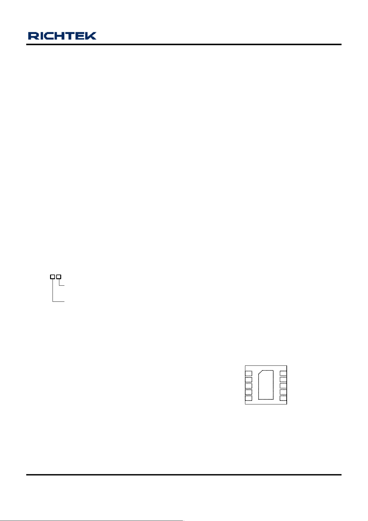
Pin Configurations
(TOP VIEW)
1
LX
2
VDD
3
NC
4
NC
5
EN
VDFN-10L 3x3
GND
10
GND
9
GND
8
GND
7
COMP
9
11
FB
DS8003-06 August 2007 www.richtek.com
1
RT8003
Typical Application Circuit
V
IN
2.4V to 4.2V
Chip Enable
Recommended component selection for Typical Application Circuit.
V
(V) VIN (V) CIN (µF) C
OUT
0.5 2.4 to 3.3
1 1/2.2 2.2/1 10 Open 10
C
1uF
C
COMP
10nF
OUT
IN
5
EN
7
(µF) L
2
VDD
LX
RT8003
FBCOMP
GND
8, 9, 10,
Exposed Pad (11)
(µH) R1 (kΩ) R2 (k Ω) C
OUT
1
6
L
2.2uH
OUT
R1
10k
R2
7.15k
V
OUT
1.2V/600mA
C
OUT
1uF
COMP
(nF)
1 2.4 to 3.6
1.2 2.4 to 4.2
1.8 2.4 to 5.5
2.5 3.3 to 5.5
3.3 4.2 to 5.5
1 1/2.2 2.2/1 10 10 10
1 1/2.2 2.2/1 10 7.15 10
1 1/2.2 2.2/1 10 3.83 10
1 1/2.2 2.2/1 10 2.49 10
1 1/2.2 2.2/1 10 1.78 10
Suggested Inductors
Component
Supplier
ABC SR0302
Sumida CDRH2D14
TDK VLP4612
Series Inductance
(µH)
1
2.2
2.2 94 1000 3.2x3.2x1.55
1
2.5
Suggested Capacitors For CIN and C
Component Supplier
TDK
C1608X5R1A105M 1 0603
Part No. Capacitance (uF) Case Size
C1608X5R1A225M 2.2 0603
Panasonic
ECJ1VB0J105M 1 0603
ECJ1VB0J225M 2.2 0603
TAIYO YUDEN
JMK107BJ105M 1 0603
JMK107BJ225M 2.2 0603
OUT
ESR
(mΩ)
60
90
110
170
Current Rating
(mA)
2100
1650
1500
1100
Dimensions
(mm)
3x2.8x2.5
4.6x3.4x1.2
DS8003-06 August 2007www.richtek.com
2
Functional Pin Description
Power Input Supply. Input voltage which supplies current to the output pin. Connect
Floating this pin is
Switcher Feedback Voltage. This pin is the inverting input of the error amplifier. FB
resistor divider network. FB
Compensation Input. This pin is the output of the internal error amplifier. Connect
and ground plane with
The exposed pad must be
).
t
signal, compensation and
RT8003
Pin No. Pin Name
1 LX Internal Power MOSFET Switches Output. Connect this pin to the inductor.
2 VDD
this pin with a low-ESR capacitor to GND
3, 4 NC No Internal Connection
5 EN
6 FB
Chip Enable (Active High). Logic low shuts down the converter.
forbidden.
senses the switcher output through an external
regulation voltage is 0.5V.
7 COMP
an external capacitor to compensate the regulator controlled loop.
Ties the pin directly to the cathode terminal of CIN and C
the lowest impedance. Signal and Common Ground (
8, 9, 10, 11
(Exposed Pad)
GND
soldered to a large PCB and connected to GND for maximum power dissipation
The GND pad area should be as large as possible and using many vias to conduc
the heat into the buried GND plate of PCB layer. All smallfeedback components should connect to this pin.
Function Block Diagram
Pin Function
OUT
COMP
FB
EN
Shutdown
Control
Oscillator
V
REF
Slope
Compensation
+
Error
Amplifier
-
Current Limit
Detector
-
PWM
Comparator
+
Over
Temperature
Detector
Control
Logic
Zero
Detector
Current
Sense
Driver
VDD
LX
GND
DS8003-06 August 2007 www.richtek.com
3
RT8003
Absolute Maximum Ratings (Note 1)
l Supply Voltage ---------------------------------------------------------------------------------------------------−0.3V to 6V
l LX Voltage---------------------------------------------------------------------------------------------------------−0.3V to (V
l Power Dissipation, P
@ T
D
= 25°C
A
VDFN-10L 3x3----------------------------------------------------------------------------------------------------1.923W
l Package Thermal Resistance (Note 2)
VDFN-10L 3x3, θJA-----------------------------------------------------------------------------------------------52°C/W
l Junction Temperature-------------------------------------------------------------------------------------------150°C
l Lead Temperature (Soldering, 10 sec.)----------------------------------------------------------------------260°C
l Storage Temperature Range-----------------------------------------------------------------------------------−65°C to 150°C
l ESD Susceptibility (Note 3)
HBM (Human Body Mode)-------------------------------------------------------------------------------------2kV
MM (Machine Mode)--------------------------------------------------------------------------------------------200V
Recommended Operating Conditions (Note 4)
l Supply Voltage---------------------------------------------------------------------------------------------------2.4V to 5.5V
l Enable Input Voltage,
l Ambient Temperature Range----------------------------------------------------------------------------------−40°C to 85°C
l Junction Temperature Range----------------------------------------------------------------------------------0°C to 125°C
-------------------------------------------------------------------------------------0V to 5.5V
VEN
DD
+ 0.3V)
Electrical Characteristics
(V
= 3.3V, T
DD
Supply Current
Quiescent Current
Shutdown Current I
Reference
Reference Voltage V
Oscillator
Switching Frequency Range
Maximum Duty Cycle DC
Output Voltage
Line Regulation
Load Regulation 10mA < I
Power Switches
R
DS(ON)
R
DS(ON)
Current Limit
= 25°C, unless otherwise specified)
A
Parameter Symbol
IQ
SHDN
REF
f
OSC
of P-Channel MOSFET R
of N-Channel MOSFET R
P_FET
N_FET
I
LIMIT
V
= 3.3V, V
EN
I
OUT
V
= 0V -- 0.01
EN
0.4925 0.5 0.5075 V
1.7 2.0 2.3 MHz
V
= V
DD
V
= 2.4V to 5.5V, I
DD
V
V
= 3.3V, ILX = 300mA
DD
V
= 3.3V, ILX = −300mA
DD
= 3.3V, V
DD
Test Conditions Min Typ Max Unit
= 0mA
OUT
LOAD
= V
FB
< 600mA -- -- +1.5
+ 0.15V,
REF
LOAD
= 100mA
90 200 400 µA
100 -- -- %
-- -- +1.5
100 230 600 mΩ
100 180 600
FB
= V
REF
- 0.15V
1.6 2 2.4 A
To be continued
1 µA
%
%
mΩ
DS8003-06 August 2007www.richtek.com
4

RT8003
Parameter Symbol
Logic Input
EN Threshold
Protection
Thermal Shutdown Temperature TSD -- 180
Thermal Shutdown Hysteresis ∆TSD -- 20 -- °C
Note 1. Stresses listed as the above "Absolute Maximum Ratings" may cause permanent damage to the device. These are for
Note 2. θJA is measured in the natural convection at TA = 25°C on a high effective thermal conductivity test board of
Note 3. Devices are ESD sensitive. Handling precaution recommended.
Note 4. The device is not guaranteed to function outside its operating conditions.
Logic-Low Voltage VIL VDD = 2.4V to 5.5V, Shutdown -- -- 0.4
Logic-High Voltage VIH VDD = 2.4V to 5.5V, Enable 1.5
stress ratings. Functional operation of the device at these or any other conditions beyond those indicated in the
operational sections of the specifications is not implied. Exposure to absolute maximum rating conditions for extended
periods may remain possibility to affect device reliability.
JEDEC 51-7 thermal measurement standard.
Test Conditions Min Typ Max Unit
V
-- --
-- °C
DS8003-06 August 2007 www.richtek.com
5

RT8003
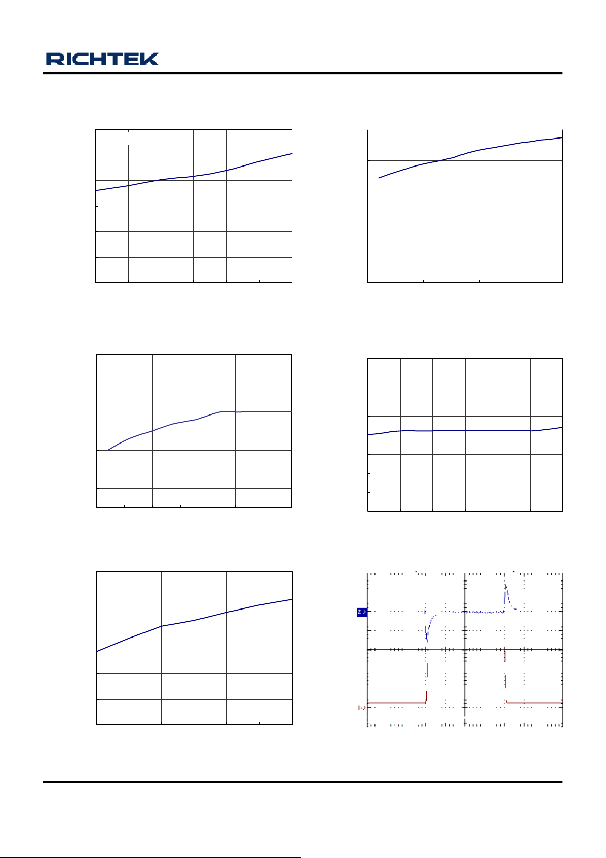
Output Voltage Deviation (%)
Typical Operating Characteristics
Output Voltage Deviation vs. Output Current
0.10%
0.1
0.00%
0
-0.10%
-0.1
-0.20%
-0.2
-0.30%
-0.3
-0.40%
-0.4
-0.50%
-0.5
-0.60%
-0.6
-0.70%
-0.7
0 100 200 300 400 500 600 700 800
Output Current (mA)
Efficiency vs. Output Current
100%
100
Efficiency (%)
VIN = 3.3V, V
90%
90
80%
80
70%
70
60%
60
50%
50
40%
40
30%
30
20%
20
10%
10
0%
0
1 10 100 1000
= 1.2V
OUT
Output Current (mA)
Output Voltage Deviation (%)
Efficiency (%)
Output Voltage Deviation vs. Temperature
0.40%
0.4
0.20%
0.2
0.00%
0
-0.20%
-0.2
-0.40%
-0.4
-0.60%
-0.6
-0.80%
-0.8
-1.00%
-1.0
-1.20%
-1.2
-1.40%
-1.4
-1.60%
-1.6
-1.80%
-1.8
-50 -25 0 25 50 75 100 125 150
Temperature
(°C)
Efficiency vs. Temperature
100%
100
90%
90
80%
80
70%
70
60%
60
50%
50
40%
40
30%
30
20%
20
10%
10
VIN = 3.3V, V
0%
0
-50 -25 0 25 50 75 100 125 150
= 1.2V, I
OUT
Temperature
= 200mA
OUT
(°C)
Frequency vs. Input Voltage
2.15
2.1
2.05
2
1.95
Frequency (MHz)
1.9
1.85
2.5 3 3.5 4 4.5 5 5.5
Input Voltage(V)
2.05
2
1.95
1.9
1.85
Frequency (MHz)
1.8
1.75
-50 -25 0 25 50 75 100 125
Frequency vs.Temperature
Temperature
(°C)
DS8003-06 August 2007www.richtek.com
6
RT8003
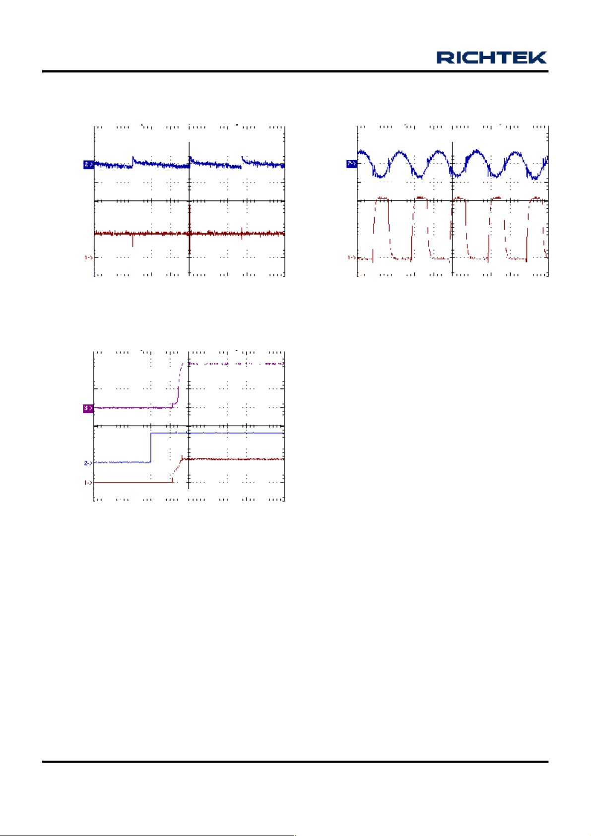
Quiescent Current vs. Input Voltage
300
VFB = 0.65V
250
200
150
100
Quiescent Current (uA)
50
0
2.5 3 3.5 4 4.5 5 5.5
Input Voltage(V)
V
vs. Temperature
0.52
0.515
0.51
0.505
(V)
0.5
REF
V
0.495
0.49
0.485
0.48
-50 -25 0 25 50 75 100 125
REF
Temperature
(°C)
Quiescent Current vs. Temperature
250
VIN = 3.3V, VFB = 0.65V
200
150
100
Quiescent Current (uA)
50
0
-50 -25 0 25 50 75 100 125
Temperature
V
vs. Input Voltage
0.52
0.515
0.51
0.505
(V)
0.5
REF
V
0.495
0.49
0.485
0.48
2.5 3 3.5 4 4.5 5 5.5
REF
Input Voltage (V)
(°C)
Current Limit vs. Input Voltage
3
2.5
Load Transient Response
VIN = 3.3V, V
I
= 50mA to 600mA
OUT
OUT
= 1.2V
Output
2
1.5
1
Current Limit (A)
0.5
0
2.5 3 3.5 4 4.5 5 5.5
Input Voltage (V)
Voltage
Load
Current
(50mV/Div)
(200mA/Div)
Time (250µs/Div)
DS8003-06 August 2007 www.richtek.com
7
RT8003
Output
Voltage
V
Output
Voltage
LX
VIN = 3.3V, V
(10mV/Div)
(1V/Div)
(500mV/Div)
Steady State
= 1.2V, I
OUT
Time (25µs/Div)
= 0mA, C
OUT
Soft Start Function
OUT
= 1uF
Output
Voltage
V
LX
VIN = 3.3V, V
(10mV/Div)
(1V/Div)
Steady State
= 1.2V, I
OUT
Time (250ns/Div)
OUT
= 600mA, C
OUT
= 1uF
V
EN
Input
Current
(2V/Div)
(200mA/Div)
V
= 3.3V, V
IN
= 1.2V, I
OUT
OUT
Time (500µs/Div)
= 600mA
DS8003-06 August 2007www.richtek.com
8

Application Information
RT8003
RT8003 is a pulse-width-modulated (PWM) step-down DCDC converter. Capable of delivering 600mA output current
over a wide input voltage range from 2.4V to 5.5V. The
RT8003 is ideally suited for portable electronic devices
that are powered from 1-cell Li-ion battery or from other
power sources within the range such as cellular phones,
PDAs and handy terminals.
Chip Enable/Disable and Soft Start
Four operational modes are available: PWM, PSM, LowDrop-Out and shut-down modes. Pulling EN pin lower than
0.4V shuts down the RT8003 and reduces its quiescent
current to 1µA. Pulling EN pin higher than 1.5V enables
the RT8003 and initiates the softstart cycle. RT8003 has
internal soft-start that can reduce the Inrush Current during
the rising of Output Voltage.
PWM Operation
During normal operation, the RT8003 regulates output
voltage by switching at a constant frequency transferring
the power to the load in each cycle by PWM. The RT8003
uses a slope-compensated, current-mode PWM controller
capable of achieving 100% duty cycle. At each rising edge
of the internal oscillator, the Control Logic cell sends a
PWM ON signal to the Driver cell to turn on internal PMOSFET. This allows current to ramp up through the
inductor to the load, and stores energy in a magnetic field.
The switch remains on until either the current-limit is
tripped or the PWM comparator signals for the output in
regulation. After the switch is turned off, the inductor
releases the magnetic energy and forces current through
the N-MOSFET synchronous rectifier to the output-filter
capacitor and load. The output-filter capacitor stores charge
when the inductor current is above the average output
current and releases charge when the inductor current is
below the average current to smooth the output voltage
across the load. A Zero Detector monitors inductor current
by sensing voltage drop across the N-MOSFET
synchronous rectifier when it turns on. The N-MOSFET
turns off and allows the converter entering discontinuous
conduction mode when the inductor current decreases to
zero. The zero current detection on threshold is about
80mA.This reduces conduction loss and increase power
conversion efficiency at light load condition.
PSM Operation
Consequently, the converter will enter pulse-skipping mode
(PSM) during extreme light load condition or when
modulation index (V
OUT/VIN
) is extreme low. This could
reduce switching loss and further increase power
conversion efficiency.
Over Current Protection
The RT8003 continuously monitors the inductor current
by sensing the voltage across the P-MOSFET when it
turns on. When the inductor current is higher than current
limit threshold (1.8A typical), OCP activates and forces
the P-MOSFET turning off to limit inductor current cycle
by cycle.But it will shut down when the V
trip the UV
OUT
protection.
Output Voltage Setting and Feedback Network
The output voltage can be set from V
divider as: the internal V
is 0.5V with 1.5% accuracy.
REF
to VIN by a voltage
REF
In practical application, keep R1 = 10kΩ respectively and
choose appropriate R2 according to the required output
voltage.
Inductor Selection
The output inductor is suggested as the table of suggested
inductors for optimal performance. Make sure that the
inductor will not saturate over the operation conditions
including temperature range, input voltage range, and
maximum output current. If possible, choose an inductor
with rated current higher than 2A so that it will not saturate
even under short circuit condition.
Input Capacitor Selection
The input capacitor can filter the input peak current and
noise at input voltage source. The capacitor with low ESR
(effective series resistance) provides the small drop voltage
to stabilize the input voltage during the transient loading.
For input capacitor selection, the ceramic capacitors larger
than 1µF is recommend. The capacitor must conform to
the RMS current requirement. The maximum RMS ripple
current is calculated as :
OUTINOUT
OUT(MAX)RMS
I I =
IN
V
) V- (V V
DS8003-06 August 2007 www.richtek.com
9

RT8003
Output Capacitor Selection
The capacitor’ s ESR determines the output ripple voltage
and the initial voltage drop following a high slew-rate
transient’ s edge. Typically, if the ESR requirement is
satisfied, the capacitance is adequate to filtering. The
output ripple voltage can be calculated as:
Where f
COUT +∆=∆
= operating frequency, C
OSC
(ESR I V
1
)
f x C x 8
OSCOUT
= output
OUT
capacitance and ∆IC = ∆IL = ripple current in the inductor.
The ceramic capacitor with low ESR value provides the
low output ripple and low size profile. Connect a 1µF/2.2µF
ceramic capacitor at output terminal for good performance
and place the input and output capacitors as close as
possible to the device.
Layout Considerations
Follow the PCB layout guidelines for optimal performance
of RT8003.
L1
LX
V
IN
C1
R4
VDD
EN
RT8003
COMP
GND
FB
C2
R1
R2
C3
V
OUT
Figure 1
1. For the main current paths as indicated in bold lines in
Figure 1, keep their traces short and wide.
2. Put the input capacitor as close as possible to the device
pins (VDD and GND).
3. LX node is with high frequency voltage swing and should
be kept small area. Keep analog components away from
LX node to prevent stray capacitive noise pick-up.
4. Connect feedback network behind the output capacitors.
Keep the loop area small. Place the feedback components
near the RT8003.
5.Connect all analog grounds to a command node and
then connect the command node to the power ground
behind the output capacitors.
6. An example of 2-layer PCB layout is shown in Figure 2
to Figure 3 for reference.
Figure 2. Top Layer
Figure 3. Bottom Layer
10
DS8003-06 August 2007www.richtek.com
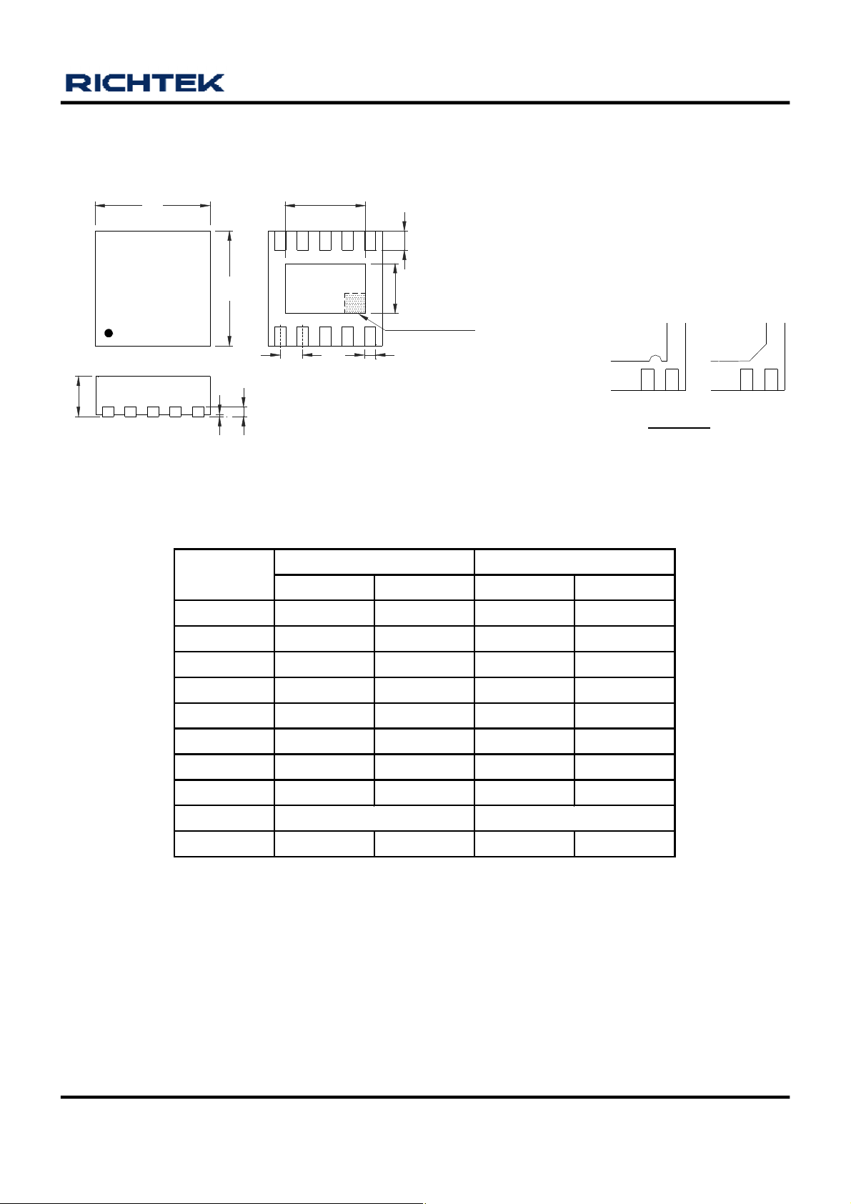
Outline Dimension
RT8003
D
E
A
A3
A1
D2
L
E2
SEE DETAIL A
1
e
b
2
1 1
2
DETAIL A
Pin #1 ID and Tie Bar Mark Options
Note : The configuration of the Pin #1 identifier is optional,
but must be located within the zone indicated.
Dimensions In Millimeters
Dimensions In Inches
Symbol
Min Max Min Max
A 0.800 1.000 0.031 0.039
A1 0.000 0.050 0.000 0.002
A3 0.175 0.250 0.007 0.010
b 0.180 0.300 0.007 0.012
D 2.950 3.050 0.116 0.120
D2 2.300 2.650 0.091 0.104
E 2.950 3.050 0.116 0.120
E2 1.500 1.750 0.059 0.069
e 0.500 0.020
L 0.350 0.450
Richtek Technology Corporation
Headquarter
5F, No. 20, Taiyuen Street, Chupei City
Hsinchu, Taiwan, R.O.C.
Tel: (8863)5526789 Fax: (8863)5526611
0.014 0.018
V-Type 10L DFN 3x3 Package
Richtek Technology Corporation
Taipei Office (Marketing)
8F, No. 137, Lane 235, Paochiao Road, Hsintien City
Taipei County, Taiwan, R.O.C.
Tel: (8862)89191466 Fax: (8862)89191465
Email: marketing@richtek.com
Information that is provided by Richtek Technology Corporation is believed to be accurate and reliable. Richtek reserves the right to make any change in circuit
design, specification or other related things if necessary without notice at any time. No third party intellectual property infringement of the applications should be
guaranteed by users when integrating Richtek products into any application. No legal responsibility for any said applications is assumed by Richtek.
DS8003-06 August 2007 www.richtek.com
11

 Loading...