

RT6211A/B
RT6211A/B
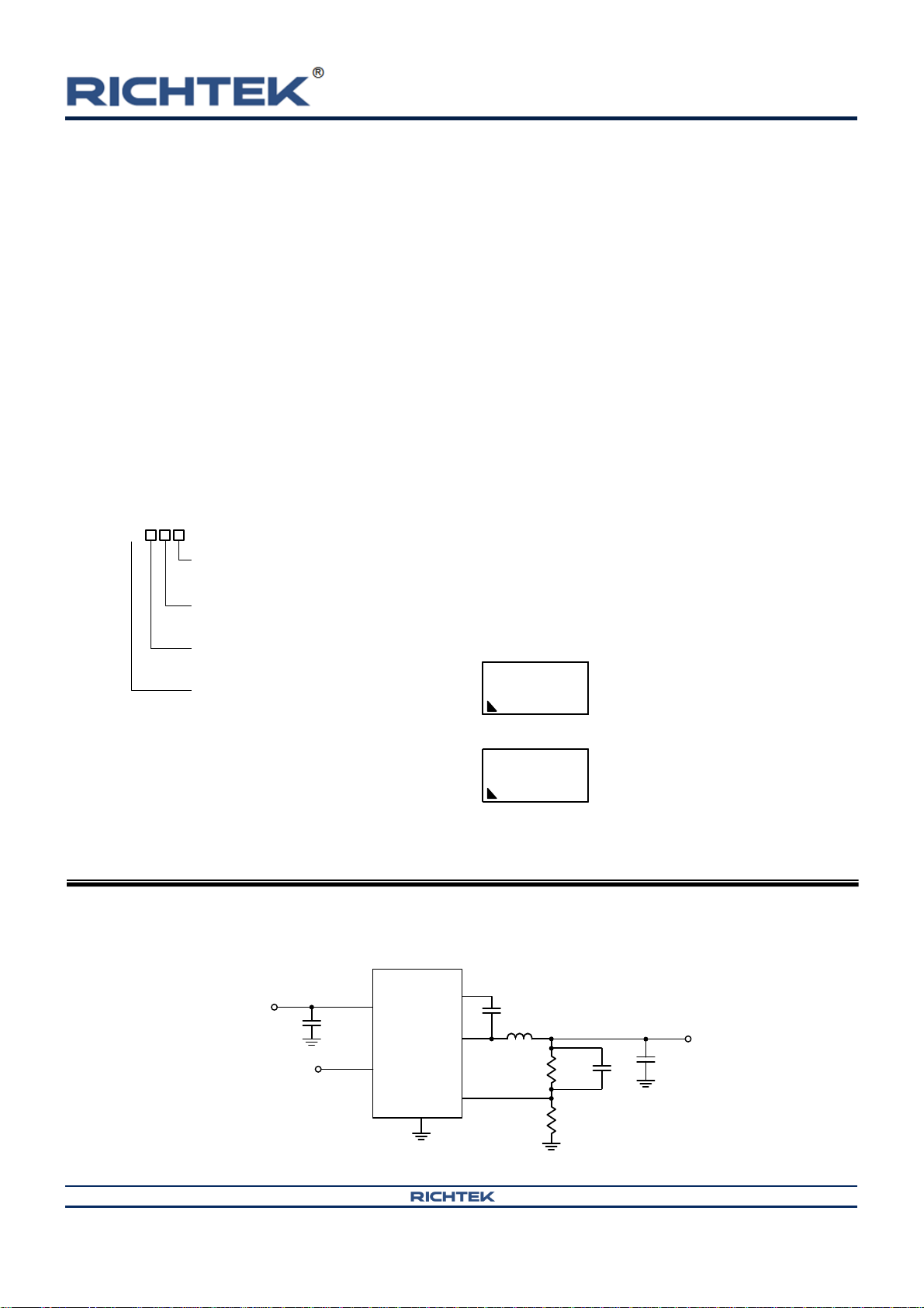
Package Type
E : SOT-23-6
Lead Plating System
G : Green (Halogen Free and Pb Free)
UVP Option
H : Hiccup
A : PSM Mode
B : PWM Mode
3J=DNN
3J= : Product Code
DNN : Date Code
RT6211AHGE
39=DNN
39= : Product Code
DNN : Date Code
RT6211BHGE
EN
RT6211A/B
GND
VIN
V
IN
C
IN
BOOT
L
C
BOOT
LX
Enable
FB
C
OUT
V
OUT
R1
R2
C
FF
1.5A, 18V, 500kHz, ACOTTM Step-Down Converter
General Description
The RT6211A/B is a high-efficiency, monolithic
synchronous step-down DC/DC converter that can
deliver up to 1.5A output current from a 4.5V to 18V
input supply. The RT6211A/B adopts ACOT
architecture to allow the transient response to be
improved and keep in constant frequency.
Cycle-by-cycle current limit provides protection against
shorted outputs and soft-start eliminates input current
surge during start-up. Fault conditions also include
output under voltage protection, output over current
protection, and thermal shutdown.
Ordering Information
Features
Integrated 230m/130m MOSFETs
4.5V to 18V Supply Voltage Range
500kHz Switching Frequency
ACOT Control
0.8V 1.5% Voltage Reference
Internal Start-Up into Pre-biased Outputs
Compact Package : SOT-23-6 pin
High/Low Side Over-Current Protection and
Hiccup
V
Range 0.8V to 6.5V
OUT
Applications
Set-Top Boxes
Portable TVs
Access Point Routers
DSL Modems
LCD TVs
Marking Information
Note :
Richtek products are :
Simplified Application Circuit
Copyright © 2015 Richtek Technology Corporation. All rights reserved. is a registered trademark of Richtek Technology Corporation.
DS6211A/B-01 March 2015 www.richtek.com
RoHS compliant and compatible with the current
requirements of IPC/JEDEC J-STD-020.
Suitable for use in SnPb or Pb-free soldering processes.
1
RT6211A/B
VIN
GND
LX
FB
ENBOOT
4
23
56
Pin No.
Pin Name
Pin Function
1
VIN
Power Input. Supplies the power switches of the device.
2
GND
System Ground. Provides the ground return path for the control circuitry and
low-side power MOSFET.
3
LX
Switch Node. LX is the switching node that supplies power to the output and
connect the output LC filter from LX to the output load.
4
BOOT
Bootstrap Supply for High-Side Gate Driver. Connect a 100nF or greater
capacitor from LX to BOOT to power the high-side switch.
5
EN
Enable Control Input. Floating this pin or connecting this pin to logic high can
enable the device and connecting this pin to GND can disable the device.
6
FB
Feedback Voltage Input. This pin is used to set the desired output voltage via
an external resistive divider. The feedback voltage is 0.8V typically.
UGATE
LGATE
Driver
LX
BOOT
PVCC
Control
On-Time
EN
Comparator
LX
GND
Reg
VIBIAS
VREF
PVCC
+
--
LX
PVCC
Ripple
Gen.
VIN
FB
Minoff
EN
VIN
GND
LX
VIN
UV &OV
OC
Pin Configurations
(TOP VIEW)
Functional Pin Description
Function Block Diagram
SOT-23-6
Copyright © 2015 Richtek Technology Corporation. All rights reserved. is a registered trademark of Richtek Technology Corporation.
www.richtek.com DS6211A/B-01 March 2015
2

RT6211A/B
Detailed Description
The RT6211A/B are high-performance 500kHz 1.5A
step-down regulators with internal power switches and
synchronous rectifiers. They feature an Advanced
Constant On-Time (ACOTTM) control architecture that
provides stable operation with ceramic output
capacitors without complicated external compensation,
among other benefits. The input voltage range is from
4.5V to 18V and the output is adjustable from 0.8V to
6.3V.
The proprietary ACOTTM control scheme improves
upon other constant on-time architectures, achieving
nearly constant switching frequency over line, load, and
output voltage ranges. The RT6211A/B are optimized
for ceramic output capacitors. Since there is no internal
clock, response to transients is nearly instantaneous
and inductor current can ramp quickly to maintain
output regulation without large bulk output capacitance.
Constant On-Time (COT) Control
The heart of any COT architecture is the on-time
one-shot. Each on-time is a pre-determined “fixed”
period that is triggered by a feedback comparator. This
robust arrangement has high noise immunity and is
ideal for low duty cycle applications. After the on-time
one-shot period, there is a minimum off-time period
before any further regulation decisions can be
considered. This arrangement avoids the need to make
any decisions during the noisy time periods just after
switching events, when the switching node (LX) rises or
falls. Because there is no fixed clock, the high-side
switch can turn on almost immediately after load
transients and further switching pulses can ramp the
inductor current higher to meet load requirements with
minimal delays.
Traditional current mode or voltage mode control
schemes typically must monitor the feedback voltage,
current signals (also for current limit), and internal
ramps and compensation signals, to determine when to
turn off the high-side switch and turn on the
synchronous rectifier. Weighing these small signals in a
switching environment is difficult to do just after
switching large currents, making those architectures
problematic at low duty cycles and in less than ideal
board layouts.
Because no switching decisions are made during noisy
time periods, COT architectures are preferable in low
duty cycle and noisy applications. However, traditional
COT control schemes suffer from some disadvantages
that preclude their use in many cases. Many
applications require a known switching frequency
range to avoid interference with other sensitive circuitry.
True constant on-time control, where the on-time is
actually fixed, exhibits variable switching frequency. In
a step-down converter, the duty factor is proportional to
the output voltage and inversely proportional to the
input voltage. Therefore, if the on-time is fixed, the
off-time (and therefore the frequency) must change in
response to changes in input or output voltage.
Modern pseudo-fixed frequency COT architectures
greatly improve COT by making the one-shot on-time
proportional to V
and inversely proportional to VIN.
OUT
In this way, an on-time is chosen as approximately
what it would be for an ideal fixed-frequency PWM in
similar input/output voltage conditions. The result is a
big improvement but the switching frequency still varies
considerably over line and load due to losses in the
switches and inductor and other parasitic effects.
Another problem with many COT architectures is their
dependence on adequate ESR in the output capacitor,
making it difficult to use highly-desirable, small,
low-cost, but low-ESR ceramic capacitors. Most COT
architectures use AC current information from the
output capacitor, generated by the inductor current
passing through the ESR, to function in a way like a
current mode control system. With ceramic capacitors,
the inductor current information is too small to keep the
control loop stable, like a current mode system with no
current information.
ACOTTM Control Architecture
Making the on-time proportional to V
and inversely
OUT
proportional to VIN is not sufficient to achieve good
constant-frequency behavior for several reasons. First,
voltage drops across the MOSFET switches and
inductor cause the effective input voltage to be less
than the measured input voltage and the effective
output voltage to be greater than the measured output
voltage. As the load changes, the switch voltage drops
Copyright © 2015 Richtek Technology Corporation. All rights reserved. is a registered trademark of Richtek Technology Corporation.
DS6211A/B-01 March 2015 www.richtek.com
3

RT6211A/B
change causing a switching frequency variation with
load current. Also, at light loads if the inductor current
goes negative, the switch dead-time between the
synchronous rectifier turn-off and the high-side switch
turn-on allows the switching node to rise to the input
voltage. This increases the effective on-time and
causes the switching frequency to drop noticeably.
One way to reduce these effects is to measure the
actual switching frequency and compare it to the
desired range. This has the added benefit eliminating
the need to sense the actual output voltage, potentially
saving one pin connection. ACOTTM uses this method,
measuring the actual switching frequency (at SW) and
modifying the on-time with a feedback loop to keep the
average switching frequency in the desired range.
To achieve good stability with low-ESR ceramic
capacitors, ACOTTM uses a virtual inductor current
ramp generated inside the IC. This internal ramp signal
replaces the ESR ramp normally provided by the output
capacitor's ESR. The ramp signal and other internal
compensations are optimized for low-ESR ceramic
output capacitors.
ACOTTM One-shot Operation
The RT6211A/B control algorithm is simple to
understand. The feedback voltage, with the virtual
inductor current ramp added, is compared to the
reference voltage. When the combined signal is less
than the reference the on-time one-shot is triggered, as
long as the minimum off-time one-shot is clear and the
measured inductor current (through the synchronous
rectifier) is below the current limit. The on-time
one-shot turns on the high-side switch and the inductor
current ramps up linearly. After the on-time, the
high-side switch is turned off and the synchronous
rectifier is turned on and the inductor current ramps
down linearly. At the same time, the minimum off-time
one-shot is triggered to prevent another immediate
on-time during the noisy switching time and allow the
feedback voltage and current sense signals to settle.
The minimum off-time is kept short (240ns typical) so
that rapidly-repeated on-times can raise the inductor
current quickly when needed.
Copyright © 2015 Richtek Technology Corporation. All rights reserved. is a registered trademark of Richtek Technology Corporation.
www.richtek.com DS6211A/B-01 March 2015
4
Discontinuous Operating Mode (RT6211A Only)
After soft-start, the RT6211B operates in fixed
frequency mode to minimize interference and noise
problems. The RT6211A uses variable-frequency
discontinuous switching at light loads to improve
efficiency. During discontinuous switching, the on-time
is immediately increased to add “hysteresis” to
discourage the IC from switching back to continuous
switching unless the load increases substantially.
The IC returns to continuous switching as soon as an
on-time is generated before the inductor current
reaches zero. The on-time is reduced back to the
length needed for 500kHz switching and encouraging
the circuit to remain in continuous conduction,
preventing repetitive mode transitions between
continuous switching and discontinuous switching.
Current Limit
The RT6211A/B current limit is a cycle-by-cycle “valley”
type, measuring the inductor current through the
synchronous rectifier during the off-time while the
inductor current ramps down. The current is
determined by measuring the voltage between Source
and Drain of the synchronous rectifier, adding
temperature compensation for greater accuracy. If the
current exceeds the current limit, the on-time one-shot
is inhibited until it drops below the current limit level. If
the output current exceeds the available inductor
current (controlled by the current limit mechanism), the
output voltage will drop. If it drops below the output
under-voltage protection level (see next section) the IC
will stop switching to avoid excessive heat.
The RT6211B also includes a negative current limit to
protect the IC against sinking excessive current and
possibly damaging the IC. If the voltage across the
synchronous rectifier indicates the negative current is
too high, the synchronous rectifier turns off until after
the next high-side on-time. The RT6211A does not sink
current and therefore does not need a negative current
limit.
Hiccup Mode
The RT6211AHGE / RT6211BHGE, use hiccup mode
UVP. When the protection function is triggered, the IC
will shut down for a period of time and then attempt to
recover automatically. Hiccup mode allows the circuit to

RT6211A/B
operate safely with low input current and power
dissipation, and then resume normal operation as soon
as the overload or short circuit is removed.
Input Under-Voltage Lockout
To protect the chip from operating at insufficient supply
voltage, the UVLO is needed. When the input voltage
of VIN is lower than the UVLO falling threshold voltage,
the device will be lockout.
Shut-down, Start-up and Enable (EN)
The enable input (EN) has a logic-low level. When VEN
is below this level the IC enters shutdown mode and
supply current drops to less than 6A. When VEN
exceeds its logic-high level the IC is fully operational.
External Bootstrap Capacitor
Connect a 0.1F low ESR ceramic capacitor between
BOOT and SW. This bootstrap capacitor provides the
gate driver supply voltage for the high side N-channel
MOSFET switch.
Over-Temperature Protection
The RT6211A/B includes an over-temperature
protection (OTP) circuitry to prevent overheating due to
excessive power dissipation. The OTP will shut down
switching operation when the junction temperature
exceeds 150C. Once the junction temperature cools
down by approximately 20C the IC will resume normal
operation. For continuous operation, provide adequate
cooling so that the junction temperature does not
exceed 150C.
UVP Protection
The RT6211A/B detects under-voltage conditions by
monitoring the feedback voltage on FB pin. The
function is enabled after approximately 1.7 times the
soft-start time. When the feedback voltage is lower
than 50% of the target voltage, the UVP comparator will
go high to turn off both internal high-side and low-side
MOSFETs.
Copyright © 2015 Richtek Technology Corporation. All rights reserved. is a registered trademark of Richtek Technology Corporation.
DS6211A/B-01 March 2015 www.richtek.com
5
RT6211A/B
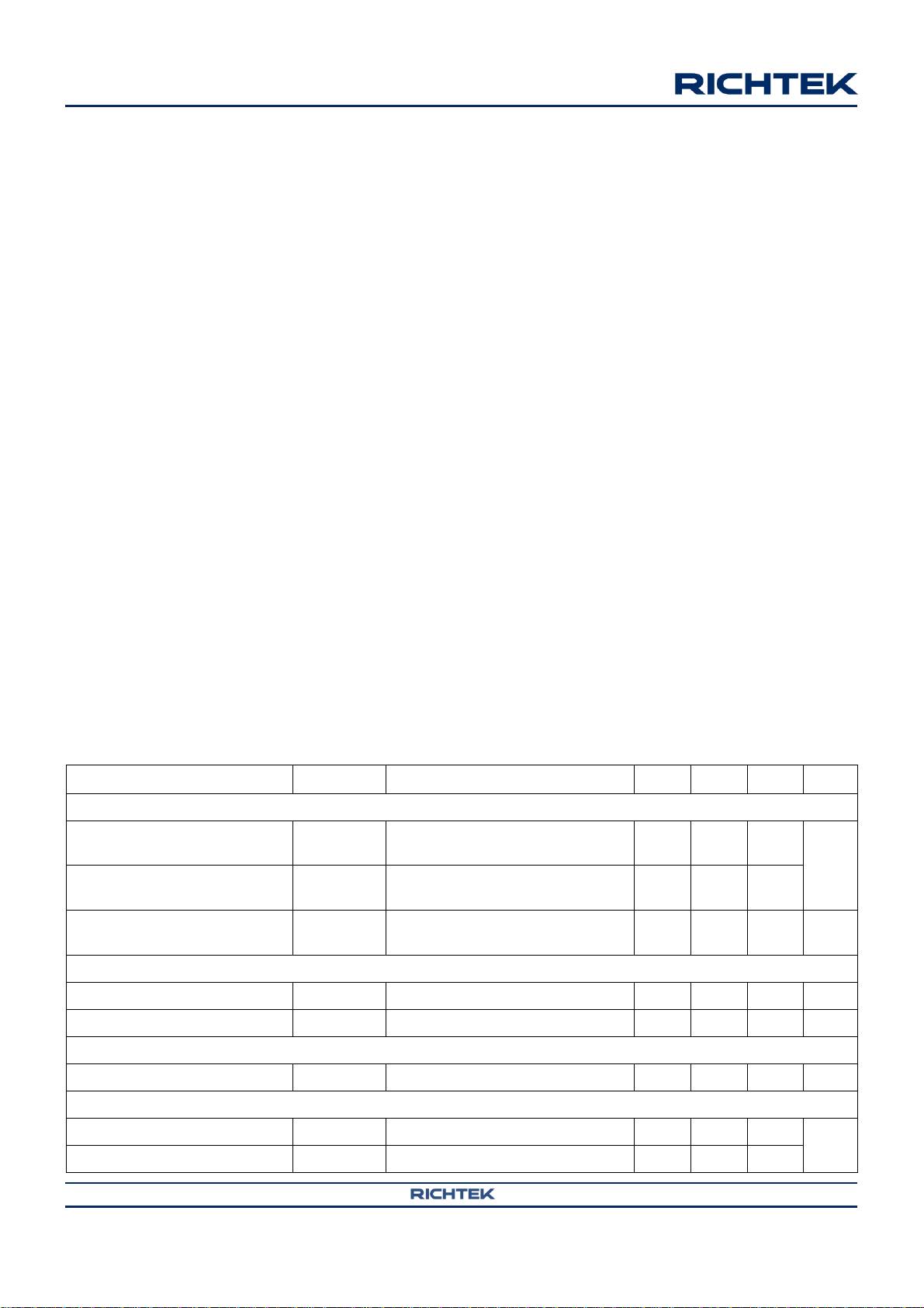
Parameter
Symbol
Test Conditions
Min
Typ
Max
Unit
Supply Voltage
VIN Supply Input Operating
Voltage
VIN 4.5
--
18
V
Under-Voltage Lockout
Threshold
V
UVLO
3.6
3.9
4.2
Under-Voltage Lockout
Threshold Hysteresis
V
UVLO
--
340
--
mV
Supply Current
Supply Current (Shutdown)
I
SHDN
VEN = 0V
--
-- 6 µA
Supply Current (Quiescent)
IQ
VEN = 2V, VFB = 0.85V
--
0.8
--
mA
Soft-Start
Soft-Start Time
--
1000
--
µs
Enable Voltage
EN Rising Threshold
V
EN_Rising
1.38
1.5
1.62
V
EN Falling Threshold
V
EN_Falling
1.16
1.28
1.4
Absolute Maximum Ratings (Note 1)
Supply Input Voltage --------------------------------------------------------------------------------- 0.3V to 20V
Switch Voltage, SW ----------------------------------------------------------------------------------- 0.8V to (V
+ 0.3V)
IN
<10ns ----------------------------------------------------------------------------------------------------- 5V to 25V
Switch Node Voltage, LX ---------------------------------------------------------------------------- 0.3V to (V
BOOT Pin Voltage ------------------------------------------------------------------------------------ (V
Other Pins ----------------------------------------------------------------------------------------------- 0.3V to 6V
Power Dissipation, P
@ TA = 25C
D
– 0.3V) to (VIN + 6.3V)
LX
+ 0.3V)
IN
SOT-23-6 ------------------------------------------------------------------------------------------------ 0.48W
Package Thermal Resistance (Note 2)
SOT-23-6, JA ------------------------------------------------------------------------------------------ 208.2C/W
Lead Temperature (Soldering, 10 sec.) ---------------------------------------------------------- 260C
Junction Temperature -------------------------------------------------------------------------------- 150C
Storage Temperature Range ----------------------------------------------------------------------- 65C to 150C
ESD Susceptibility (Note 3)
HBM (Human Body Model) ------------------------------------------------------------------------- 2kV
Recommended Operating Conditions (Note 4)
Supply Input Voltage --------------------------------------------------------------------------------- 4.5V to 18V
Ambient Temperature Range----------------------------------------------------------------------- 40C to 85C
Junction Temperature Range ---------------------------------------------------------------------- 40C to 125C
Electrical Characteristics
(VIN = 12V, TA = 25C, unless otherwise specified)
Copyright © 2015 Richtek Technology Corporation. All rights reserved. is a registered trademark of Richtek Technology Corporation.
www.richtek.com DS6211A/B-01 March 2015
6

RT6211A/B
Parameter
Symbol
Test Conditions
Min
Typ
Max
Unit
Feedback Threshold Voltage
Feedback Threshold Voltage
V
FB_TH
4.5V ≤ VIN ≤ 18V
0.788
0.8
0.812
V
Internal MOSFET
High-Side On-Resistance
R
DS(ON)_H
V
BOOT
− VLX = 4.8V
--
230
--
mΩ
Low-Side On-Resistance
R
DS(ON)_L
--
130
--
Current Limit
Current Limit
I
LIM
Valley Current
2
2.5
--
A
Switching Frequency
Switching Frequency
f
OSC
420
520
620
kHz
On-Time Timer Control
Maximum Duty Cycle
D
MAX
85
88
--
%
Minimum On Time
t
ON(MIN)
--
60
--
nS
Minimum Off Time
t
OFF(MIN)
--
240
--
Output Under Voltage Protections
UVP Trip Threshold
UVP Detect
45
50
55
%
Hysteresis
--
10
--
Thermal Shutdown
Thermal Shutdown Threshold
TSD --
150
--
°C
Thermal Shutdown Hysteresis
TSD --
20
--
Note 1. Stresses beyond those listed “Absolute Maximum Ratings” may cause permanent damage to the device. These are
stress ratings only, and functional operation of the device at these or any other conditions beyond those indicated in the
operational sections of the specifications is not implied. Exposure to absolute maximum rating conditions may affect
device reliability.
Note 2. JA is measured at TA = 25C on a high effective thermal conductivity four-layer test board per JEDEC 51-7.
Note 3. Devices are ESD sensitive. Handling precaution recommended.
Note 4. The device is not guaranteed to function outside its operating conditions.
Copyright © 2015 Richtek Technology Corporation. All rights reserved. is a registered trademark of Richtek Technology Corporation.
DS6211A/B-01 March 2015 www.richtek.com
7

RT6211A/B
EN
RT6211A/B
FB
GND
VIN
V
IN
22μF
C
IN
BOOT
L
0.1μF
C
BOOT
22μF
C
OUT
LX
V
OUT
R1
R2
1
5
2
3
4
6
Enable
C
FF
2.2μH
12k
24k
Open
1.2V/1.5A
V
OUT
(V)
R1 (k)
R2 (k)
L (H)
C
OUT
(F)
CFF (pF)
1.05
10
32.4 2 22
--
1.2
20.5
41.2 2 22
--
1.8
40.2
32.4
3.3
22
--
2.5
40.2
19.1
4.7
22
22 to 68
3.3
40.2
13
6.5
22
22 to 68
5
40.2
7.68
6.5
22
22 to 68
Typical Application Circuit
Table 1. Suggested Component Values (VIN = 12V)
Copyright © 2015 Richtek Technology Corporation. All rights reserved. is a registered trademark of Richtek Technology Corporation.
www.richtek.com DS6211A/B-01 March 2015
8

RT6211A/B
Efficiency vs. Output Current
0
10
20
30
40
50
60
70
80
90
100
0 0.3 0.6 0.9 1.2 1.5
Output Current (A)
Efficiency(%)
RT6211AH, I
OUT
= 0 to 1.5A
V
OUT
= 1.2V
V
OUT
= 5V
Output Voltage vs. Input Voltage
1.10
1.12
1.14
1.16
1.18
1.20
1.22
1.24
1.26
1.28
1.30
4 6 8 10 12 14 16 18
Input Voltage (V)
Output Voltage (V)
I
OUT
= 0.6A
I
OUT
= 0.9A
I
OUT
= 1.5A
V
OUT
= 1.2V
Output Voltage vs. Output Current
1.00
1.05
1.10
1.15
1.20
1.25
1.30
1.35
1.40
1.45
1.50
0 0.3 0.6 0.9 1.2 1.5
Output Current (A)
Output Voltage (V)
VIN = 12V
VIN = 18V
V
OUT
= 1.2V
Quiescent Current vs. Input Voltage
300
400
500
600
700
800
900
1000
1100
1200
4 6 8 10 12 14 16 18
Input Volatage (V)
Quiescent Current (μA)
1
V
OUT
= 1.2V
Frequency vs. Input Voltage
400
420
440
460
480
500
520
540
560
580
600
4 6 8 10 12 14 16 18
Input Voltage (V)
Frequency (kHz)
1
V
OUT
= 1.2V
Frequency vs. Temperature
400
420
440
460
480
500
520
540
560
580
600
-50 -25 0 25 50 75 100 125
Temperature (°C)
Frequency (kHz)
1
V
OUT
= 1.2V
VIN = 12V
VIN = 18V
Typical Operating Characteristics
Copyright © 2015 Richtek Technology Corporation. All rights reserved. is a registered trademark of Richtek Technology Corporation.
DS6211A/B-01 March 2015 www.richtek.com
9

RT6211A/B
VIN= 12V, V
OUT
= 1.2V,
I
OUT
= 0.75A to 1.5A, L = 2.3H
Load Transient Response
Time (100s/Div)
V
OUT
(50mV/Div)
I
OUT
(1A/Div)
VIN= 12V, V
OUT
= 5V,
I
OUT
= 0.75A to 1.5A, L = 6.8H
Load Transient Response
Time (100s/Div)
V
OUT
(200mV/Div)
I
OUT
(1A/Div)
VIN= 12V, V
OUT
= 1.2V, I
OUT
= 0.5A
Output Ripple Voltage
Time (1s/Div)
V
OUT
(10mV/Div)
I
LX
(500mA/Div)
V
LX
(5V/Div)
VIN= 12V, V
OUT
= 5V, I
OUT
= 1.5A, L = 6.8H
Output Ripple Voltage
Time (1s/Div)
V
LX
(5V/Div)
V
OUT
(10mV/Div)
I
LX
(500mA/Div)
VIN= 12V, V
OUT
= 5V, I
OUT
= 1.5A
Power On from EN
Time (500s/Div)
V
EN
(5V/Div)
V
OUT
(2V/Div)
VIN= 12V, V
OUT
= 1.2V, I
OUT
= 1.5A
Power Off from EN
Time (10s/Div)
V
EN
(5V/Div)
I
LX
(1A/Div)
V
LX
(20V/Div)
V
OUT
(1V/Div)
Copyright © 2015 Richtek Technology Corporation. All rights reserved. is a registered trademark of Richtek Technology Corporation.
www.richtek.com DS6211A/B-01 March 2015
10

RT6211A/B
OUT IN OUT
IN SW L
V V V
L =
V f I
OUT IN OUT
L
L L(PEAK) OUT(MAX)
IN SW
V V V
I
I = and I = I
V f L 2
1.2 12 1.2
L 4.8μH
12 500kHz 0.45A
L
1.2 12 1.2
I = = 0.45A
12 500kHz 4.8μH
L(PEAK)
0.45A
and I = 1.5A = 1.725A
2
OUT
IN
RMS OUT(MAX)
IN OUT
V
V
I = I 1
VV
Application Information
Inductor Selection
Selecting an inductor involves specifying its inductance
and also its required peak current. The exact inductor
value is generally flexible and is ultimately chosen to
obtain the best mix of cost, physical size, and circuit
efficiency. Lower inductor values benefit from reduced
size and cost and they can improve the circuit's
transient response, but they increase the inductor
ripple current and output voltage ripple and reduce the
efficiency due to the resulting higher peak currents.
Conversely, higher inductor values increase efficiency,
but the inductor will either be physically larger or have
higher resistance since more turns of wire are required
and transient response will be slower since more time
is required to change current (up or down) in the
inductor. A good compromise between size, efficiency,
and transient response is to use a ripple current (IL)
about 20% to 50% of the desired full output load
current. Calculate the approximate inductor value by
selecting the input and output voltages, the switching
frequency (fSW), the maximum output current
(I
OUT(MAX)
) and estimating a IL as some percentage of
that current.
meet the desired output current. If needed, reduce the
inductor ripple current (IL) to increase the average
inductor current (and the output current) while ensuring
that I
L(PEAK)
does not exceed the upper current limit
level.
For best efficiency, choose an inductor with a low DC
resistance that meets the cost and size requirements.
For low inductor core losses some type of ferrite core is
usually best and a shielded core type, although
possibly larger or more expensive, will probably give
fewer EMI and other noise problems.
Considering the Typical Operating Circuit for 1.2V
output at 1.5A and an input voltage of 12V, using an
inductor ripple of 0.45A (30%), the calculated
inductance value is :
The ripple current was selected at 0.45A and, as long
as we use the calculated 4.8H inductance, that should
be the actual ripple current amount. The ripple current
and required peak current as below :
Once an inductor value is chosen, the ripple current
(IL) is calculated to determine the required peak
inductor current.
To guarantee the required output current, the inductor
needs a saturation current rating and a thermal rating
that exceeds I
L(PEAK)
. These are minimum requirements.
To maintain control of inductor current in overload and
short circuit conditions, some applications may desire
current ratings up to the current limit value. However,
the IC's output under-voltage shutdown feature make
this unnecessary for most applications.
I
L(PEAK)
should not exceed the minimum value of IC's
upper current limit level or the IC may not be able to
For the 4.8H value, the inductor's saturation and
thermal rating should exceed 1.725A. Since the actual
value used was 4.8H and the ripple current exactly
0.45A, the required peak current is 1.725A.
Input Capacitor Selection
The input filter capacitors are needed to smooth out the
switched current drawn from the input power source
and to reduce voltage ripple on the input. The actual
capacitance value is less important than the RMS
current rating (and voltage rating, of course). The RMS
input ripple current (I
) is a function of the input
RMS
voltage, output voltage, and load current :
Copyright © 2015 Richtek Technology Corporation. All rights reserved. is a registered trademark of Richtek Technology Corporation.
DS6211A/B-01 March 2015 www.richtek.com
11
RT6211A/B
RIPPLE RIPPLE(ESR) RIPPLE(C)
RIPPLE(ESR) L ESR
L
RIPPLE(C)
OUT SW
V = V V
V = I R
I
V =
8 C f
RIPPLE(ESR)
RIPPLE(C)
RIPPLE
V = 0.45A 5m = 2.25mV
0.45A
V = = 2.557mV
8 44μF 500kHz
V = 2.25mV 2.557mV = 4.807mV
11
OUT
IN
3 5.23 10
C
VL
Ceramic capacitors are most often used because of
their low cost, small size, high RMS current ratings, and
robust surge current capabilities. However, take care
when these capacitors are used at the input of circuits
supplied by a wall adapter or other supply connected
through long, thin wires. Current surges through the
inductive wires can induce ringing at the RT6211A/B
input which could potentially cause large, damaging
voltage spikes at VIN. If this phenomenon is observed,
some bulk input capacitance may be required. Ceramic
capacitors (to meet the RMS current requirement) can
be placed in parallel with other types such as tantalum,
electrolytic, or polymer (to reduce ringing and
overshoot).
Choose capacitors rated at higher temperatures than
required. Several ceramic capacitors may be paralleled
to meet the RMS current, size, and height requirements
of the application. The typical operating circuit uses two
10F and one 0.1F low ESR ceramic capacitors on
the input.
Output Capacitor Selection
The RT6211A/B are optimized for ceramic output
capacitors and best performance will be obtained using
them. The total output capacitance value is usually
determined by the desired output voltage ripple level
and transient response requirements for sag
(undershoot on positive load steps) and soar
(overshoot on negative load steps).
Output Ripple
Output ripple at the switching frequency is caused by
the inductor current ripple and its effect on the output
capacitor's ESR and stored charge. These two ripple
components are called ESR ripple and capacitive ripple.
Since ceramic capacitors have extremely low ESR and
relatively little capacitance, both components are
similar in amplitude and both should be considered if
ripple is critical.
For the Typical Operating Circuit for 1.2V output and an
inductor ripple of 0.45A, with 2 x 22F output
capacitance each with about 5m ESR including PCB
trace resistance, the output voltage ripple components
are :
Output Capacitors Stability Criteria
The e RT6211A/B's ACOTTM control architecture uses
an internal virtual inductor current ramp and other
compensation that ensures stability with any
reasonable output capacitor. The internal ramp allows
the IC to operate with very low ESR capacitors and the
IC is stable with very small capacitances. Therefore,
output capacitor selection is nearly always a matter of
meeting output voltage ripple and transient response
requirements, as discussed in the previous sections.
For the sake of the unusual application where ripple
voltage is unimportant and there are few transients
(perhaps battery charging or LED lighting) the stability
criteria are discussed below.
The equations giving the minimum required
capacitance for stable operation include a term that
depends on the output capacitor's ESR. The higher the
ESR, the lower the capacitance can be and still ensure
stability. The equations can be greatly simplified if the
ESR term is removed by setting ESR to zero. The
resulting equation gives the worst-case minimum
required capacitance and it is usually sufficiently small
that there is usually no need for the more exact
equation :
Copyright © 2015 Richtek Technology Corporation. All rights reserved. is a registered trademark of Richtek Technology Corporation.
www.richtek.com DS6211A/B-01 March 2015
12
The worst-case high capacitance requirement is for low
VIN and small inductance, so a 12V to 1.2V converter
is used for an example. Using the inductance equation
in a previous section to determine the required
inductance :

RT6211A/B
1.2 12 1.2
L = = 5.4μH
12 500kHz 0.4A
11
OUT
OUT
3 5.23 10
C
12V 5.4μH
C 2.42μF
RT6211A/B
GND
FB
R1
R2
V
OUT
C
ff
BW
ff
1
C
2 3.1412 R1 BW 0.8
RT6211A/B
EN
GND
V
IN
R
EN
C
EN
EN
RT6211A/B
EN
GND
100k
V
IN
R
EN
Q1
Enable
RT6211A/B
EN
GND
V
IN
R
EN1
R
EN2
Therefore, the required minimum capacitance for the
12V to 1.2V converter is :
Feed-forward Capacitor (Cff)
The RT6211A/B are optimized for ceramic output
capacitors and for low duty cycle applications. However
for high-output voltages, with high feedback attenuation,
the circuit's response becomes over-damped and
transient response can be slowed. In high-output
voltage circuits (V
> 3.3V) transient response is
OUT
improved by adding a small “feed-forward” capacitor
(Cff) across the upper FB divider resistor (Figure 1), to
increase the circuit's Q and reduce damping to speed
up the transient response without affecting the
steady-state stability of the circuit. Choose a suitable
capacitor value that following below step.
Get the BW the quickest method to do transient
response form no load to full load. Confirm the
damping frequency. The damping frequency is BW.
Enable Operation (EN)
For automatic start-up the high-voltage EN pin can be
connected to VIN, through a 100k resistor. Its large
hysteresis band makes EN useful for simple delay and
timing circuits. EN can be externally pulled to VIN by
adding a resistor-capacitor delay (REN and CEN in
Figure 2). Calculate the delay time using EN's internal
threshold where switching operation begins.
An external MOSFET can be added to implement
digital control of EN when no system voltage above 2V
is available (Figure 3). In this case, a 100k pull-up
resistor, REN, is connected between VIN and the EN
pin. MOSFET Q1 will be under logic control to pull
down the EN pin. To prevent enabling circuit when VIN
is smaller than the VOUT target value or some other
desired voltage level, a resistive voltage divider can be
placed between the input voltage and ground and
connected to EN to create an additional input under
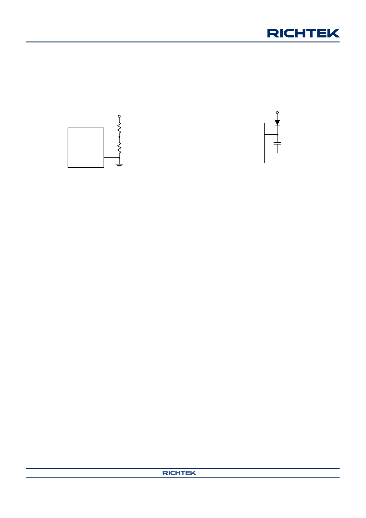
voltage lockout threshold (Figure 4).
Figure 1. Cff Capacitor Setting
C
can be calculated base on below equation :
ff
Copyright © 2015 Richtek Technology Corporation. All rights reserved. is a registered trademark of Richtek Technology Corporation.
DS6211A/B-01 March 2015 www.richtek.com
Figure 2. External Timing Control
Figure 3. Digital Enable Control Circuit
Figure 4. Resistor Divider for Lockout Threshold
Setting
13
RT6211A/B
RT6211A/B
GND
FB
R1
R2
V
OUT
OUT REF
REF
R2 (V V )
R1
V
LX
BOOT
5V
0.1μF
RT6211A/B
Output Voltage Setting
Set the desired output voltage using a resistive divider
from the output to ground with the midpoint connected
to FB. The output voltage is set according to the
following equation :
V
= 0.8V x (1 + R1 / R2)
OUT
Figure 5. Output Voltage Setting
Place the FB resistors within 5mm of the FB pin.
Choose R2 between 10k and 100k to minimize
power consumption without excessive noise pick-up
and calculate R1 as follows :
For output voltage accuracy, use divider resistors with
1% or better tolerance.
External BOOT Bootstrap Diode
When the input voltage is lower than 5.5V it is
recommended to add an external bootstrap diode
between VIN (or VINR) and the BOOT pin to improve
enhancement of the internal MOSFET switch and
improve efficiency. The bootstrap diode can be a low
cost one such as 1N4148 or BAT54.
External BOOT Capacitor Series Resistance
The internal power MOSFET switch gate driver is
optimized to turn the switch on fast enough for low
power loss and good efficiency, but also slow enough
to reduce EMI. Switch turn-on is when most EMI occurs
since VLX rises rapidly. During switch turn-off, LX is
discharged relatively slowly by the inductor current
during the dead time between high-side and low-side
switch on-times. In some cases it is desirable to reduce
EMI further, at the expense of some additional power
dissipation. The switch turn-on can be slowed by
placing a small (<47) resistance between BOOT and
the external bootstrap capacitor. This will slow the
high-side switch turn-on and VLX's rise. To remove the
resistor from the capacitor charging path (avoiding poor
enhancement due to undercharging the BOOT
capacitor), use the external diode shown in Figure 6 to
charge the BOOT capacitor and place the resistance
between BOOT and the capacitor/diode connection.
Figure 6. External Bootstrap Diode
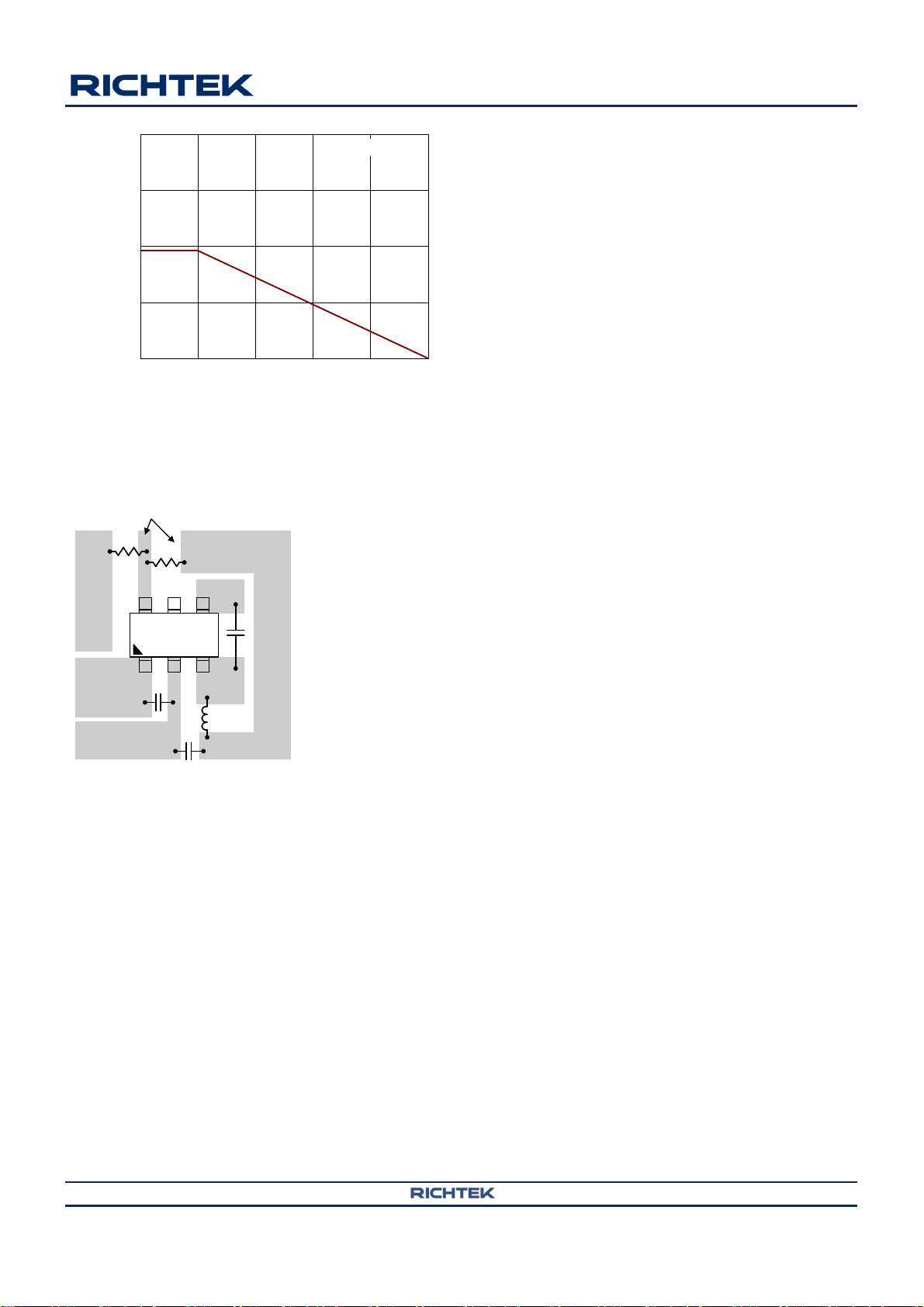
Thermal Considerations
For continuous operation, do not exceed absolute
maximum junction temperature. The maximum power
dissipation depends on the thermal resistance of the IC
package, PCB layout, rate of surrounding airflow, and
difference between junction and ambient temperature.
The maximum power dissipation can be calculated by
the following formula :
P
where T
TA is the ambient temperature, and
D(MAX)
= (T
J(MAX)
TA) / JA
J(MAX)
is the maximum junction temperature,
is the junction to
JA
ambient thermal resistance.
For recommended operating condition specifications,
the maximum junction temperature is 125C. The
junction to ambient thermal resistance, JA, is layout
dependent. For SOT-23-6 package, the thermal
resistance, JA, is 208.2C/W on a standard four-layer
thermal test board. The maximum power dissipation at
TA = 25C can be calculated by the following formula :
P
= (125C 25C) / (208.2C/W) = 0.48W for
D(MAX)
SOT-23-6 package
The maximum power dissipation depends on the
operating ambient temperature for fixed T
J(MAX)
and
thermal resistance, JA. The derating curve in Figure 7
allows the designer to see the effect of rising ambient
temperature on the maximum power dissipation.
Copyright © 2015 Richtek Technology Corporation. All rights reserved. is a registered trademark of Richtek Technology Corporation.
www.richtek.com DS6211A/B-01 March 2015
14
RT6211A/B
V
OUT
GND
VIN
GND
LX
FB
EN BOOT
4
2 3
56
Place the feedback as close
to the IC as possible.
R1
R2
C
BOOT
L
V
OUT
GND
V
IN
C
IN
C
OUT
Place the input and output capacitors
as close to the IC as possible.
LX should be connected
to inductor by wide and
short trace, and keep
sensitive components
away from this trace.
0.00
0.25
0.50
0.75
1.00
0 25 50 75 100 125
Ambient Temperature (°C)
Maximum Power Dissipation (W)
1
Four-Layer PCB
Figure 7. Derating Curve of Maximum Power
Dissipation
Figure 8. PCB Layout Guide
Copyright © 2015 Richtek Technology Corporation. All rights reserved. is a registered trademark of Richtek Technology Corporation.
DS6211A/B-01 March 2015 www.richtek.com
15

RT6211A/B
Symbol
Dimensions In Millimeters
Dimensions In Inches
Min
Max
Min
Max
A
0.889
1.295
0.031
0.051
A1
0.000
0.152
0.000
0.006
B
1.397
1.803
0.055
0.071
b
0.250
0.560
0.010
0.022
C
2.591
2.997
0.102
0.118
D
2.692
3.099
0.106
0.122
e
0.838
1.041
0.033
0.041
H
0.080
0.254
0.003
0.010
L
0.300
0.610
0.012
0.024
Outline Dimension
SOT-23-6 Surface Mount Package
Richtek Technology Corporation
14F, No. 8, Tai Yuen 1st Street, Chupei City
Hsinchu, Taiwan, R.O.C.
Tel: (8863)5526789
Richtek products are sold by description only. Richtek reserves the right to change the circuitry and/or specifications without notice at any time. Customers should
obtain the latest relevant information and data sheets before placing orders and should verify that such information is current and complete. Richtek cannot assume
responsibility for use of any circuitry other than circuitry entirely embodied in a Richtek product. Information furnished by Richtek is believed to be accurate and
reliable. However, no responsibility is assumed by Richtek or its subsidiaries for its use; nor for any infringements of patents or other rights of third parties which may
result from its use. No license is granted by implication or otherwise under any patent or patent rights of Richtek or its subsidiaries.
Copyright © 2015 Richtek Technology Corporation. All rights reserved. is a registered trademark of Richtek Technology Corporation.
www.richtek.com DS6211A/B-01 March 2015
16

 Loading...