

Page 1
E2 Emulator, E2 Emulator Lite
Supported Devices:
Rev.1.00 Mar 2020
All information contained in these materials, including products and product specifications,
Corporation. website (http://www.renesas.com).
RA Family
Additional Document for User’s Manual
(Notes on Connection of RA Devices)
represents information on the product at the time of publication and is subject to change by
Renesas Electronics Corporation. without notice. Please review the latest information published
by Renesas Electronics Corporation. through various means, including the Renesas Electronics
Page 2

Corporate Headquarters
Contact information
Trademarks
Notice
1. Descriptions of circuits, software and other related information in this document are provided only to illustrate the operation of semiconductor products
and application examples. You are fully responsible for the incorporation or any other use of the circuits, software, and information in the design of your
product or system. Renesas Electronics disclaims any and all liability for any losses and damages incurred by you or third parties arising from the use
of these circuits, software, or information.
2. Renesas Electronics hereby expressly disclaims any warranties against and liability for infringement or any other claims involving patents, copyrights,
or other intellectual property rights of third parties, by or arising from the use of Renesas Electronics products or technical information described in this
document, including but not limited to, the product data, drawings, charts, programs, algorithms, and application examples.
3. No license, express, implied or otherwise, is granted hereby under any patents, copyrights or other intellectual property rights of Renesas Electronics
or others.
4. You shall not alter, modify, copy, or reverse engineer any Renesas Electronics product, whether in whole or in part. Renesas Electronics disclaims any
and all liability for any losses or damages incurred by you or third parties arising from such alteration, modification, copying or reverse engineering.
5. Renesas Electronics products are classified according to the following two quality grades: “Standard” and “High Quality”. The intended applications for
each Renesas Electronics product depends on the product’s quality grade, as indicated below.
"Standard": Computers; office equipment; communications equipment; test and measurement equipment; audio and visual equipment; home
"High Quality": Transportation equipment (automobiles, trains, ships, etc.); traffic control (traffic lights); large-scale communication equipment; key
Unless expressly designated as a high reliability product or a product for harsh environments in a Renesas Electronics data sheet or other Renesas
Electronics document, Renesas Electronics products are not intended or authorized for use in products or systems that may pose a direct threat to
human life or bodily injury (artificial life support devices or systems; surgical implantations; etc.), or may cause serious property damage (space
system; undersea repeaters; nuclear power control systems; aircraft control systems; key plant systems; military equipment; etc.). Renesas Electronics
disclaims any and all liability for any damages or losses incurred by you or any third parties arising from the use of any Renesas Electronics product
that is inconsistent with any Renesas Electronics data sheet, user’s manual or other Renesas Electronics document.
6. When using Renesas Electronics products, refer to the latest product information (data sheets, user’s manuals, application notes, “General Notes for
Handling and Using Semiconductor Devices” in the reliability handbook, etc.), and ensure that usage conditions are within the ranges specified by
Renesas Electronics with respect to maximum ratings, operating power supply voltage range, heat dissipation characteristics, installation, etc. Renesas
Electronics disclaims any and all liability for any malfunctions, failure or accident arising out of the use of Renesas Electronics products outside of such
specified ranges.
7. Although Renesas Electronics endeavors to improve the quality and reliability of Renesas Electronics products, semiconductor products have specific
characteristics, such as the occurrence of failure at a certain rate and malfunctions under certain use conditions. Unless designated as a high reliability
product or a product for harsh environments in a Renesas Electronics data sheet or other Renesas Electronics document, Renesas Electronics
products are not subject to radiation resistance design. You are responsible for implementing safety measures to guard against the possibility of bodily
injury, injury or damage caused by fire, and/or danger to the public in the event of a failure or malfunction of Renesas Electronics products, such as
safety design for hardware and software, including but not limited to redundancy, fire control and malfunction prevention, appropriate treatment for
aging degradation or any other appropriate measures. Because the evaluation of microcomputer software alone is very difficult and impractical, you are
responsible for evaluating the safety of the final products or systems manufactured by you.
8. Please contact a Renesas Electronics sales office for details as to environmental matters such as the environmental compatibility of each Renesas
Electronics product. You are responsible for carefully and sufficiently investigating applicable laws and regulations that regulate the inclusion or use of
controlled substances, including without limitation, the EU RoHS Directive, and using Renesas Electronics products in compliance with all these
applicable laws and regulations. Renesas Electronics disclaims any and all liability for damages or losses occurring as a result of your noncompliance
with applicable laws and regulations.
9. Renesas Electronics products and technologies shall not be used for or incorporated into any products or systems whose manufacture, use, or sale is
prohibited under any applicable domestic or foreign laws or regulations. You shall comply with any applicable export control laws and regulations
promulgated and administered by the governments of any countries asserting jurisdiction over the parties or transactions.
10. It is the responsibility of the buyer or distributor of Renesas Electronics products, or any other party who distributes, disposes of, or otherwise sells or
transfers the product to a third party, to notify such third party in advance of the contents and conditions set forth in this document.
11. This document shall not be reprinted, reproduced or duplicated in any form, in whole or in part, without prior written consent of Renesas Electronics.
12. Please contact a Renesas Electronics sales office if you have any questions regarding the information contained in this document or Renesas
Electronics products.
(Note1) “Renesas Electronics” as used in this document means Renesas Electronics Corporation and also includes its directly or indirectly controlled
(Note2) “Renesas Electronics product(s)” means any product developed or manufactured by or for Renesas Electronics.
subsidiaries.
electronic appliances; machine tools; personal electronic equipment; industrial robots; etc.
financial terminal systems; safety control equipment; etc.
(Rev.4.0-1 November 2017)
TOYOSU FORESIA, 3-2-24 Toyosu,
Koto-ku, Tokyo 135-0061, Japan
www.renesas.com
Renesas and the Renesas logo are trademarks of Renesas
Electronics Corporation. All trademarks and registered trademarks
are the property of their respective owners.
For further information on a product, technology, the most up-to-date
version of a document, or your nearest sales office, please visit:
www.renesas.com/contact/
.
Page 3

Table of Contents
1. Overview .......................................................................................................................... 5
1.1 Overview of E2 Emulator and E2 Emulator Lite ...................................................................................... 5
1.2 Configuration of E2/E2 Lite Manuals ....................................................................................................... 5
1.3 Preparation .............................................................................................................................................. 6
1.4 Supported Devices ................................................................................................................................... 6
2. Designing the User System ............................................................................................. 7
2.1 Connecting the Emulator with the User System ...................................................................................... 7
2.2 Installing the Connector on the User System .......................................................................................... 7
2.2.1 Connecting the User System Interface Cable to the 20-Pin Connector ........................................ 8
2.3 Pin Assignments of the Connector on the User System .......................................................................... 9
2.3.1 20-Pin and 10-Pin Connector Specifications ................................................................................. 9
2.4 Recommended Circuit between the Connector and the MCU............................................................... 12
2.4.1 SWD Interface Connection ........................................................................................................... 13
2.4.2 JTAG Interface Connection .......................................................................................................... 14
2.5 Notes on Connection ............................................................................................................................. 15
2.5.1 RES Pin ........................................................................................................................................ 15
2.5.2 MD Pin .......................................................................................................................................... 16
2.5.3 GND ............................................................................................................................................. 17
2.5.4 VCC .............................................................................................................................................. 17
2.5.5 RxD9 and TxD9 Pins (Flash Programming via an SCI) ............................................................... 17
2.6 Internal Circuits of the Emulator ............................................................................................................ 18
2.6.1 Internal Circuits of the E2 ............................................................................................................. 18
2.6.2 Internal Circuits of the E2 Lite ...................................................................................................... 19
3. Notes on Usage ............................................................................................................. 20
3.1 Turning the Power On/Off ...................................................................................................................... 20
3.1.1 When a Separate Power Supply is Used for the User System .................................................... 20
3.1.2 When Power is Supplied to the User System from the Emulator ................................................ 21
3.2 Power Supply Function of the E2/E2 Lite .............................................................................................. 21
3.3 Notes on Using the Emulator Debugger ................................................................................................ 22
3.3.1 Notes on Connecting the Emulator Debugger ............................................................................. 23
3.3.2 Notes on a Debugging Operation that Involves Reprogramming of Flash Memory .................... 24
3.3.3 Note on Using Software Breaks in the On-Chip SRAM ............................................................... 26
3.3.4 Notes on Using Software Breaks (Common to the On-Chip SRAM and Flash Memory) ............ 27
3.3.5 Note on Peripheral I/O Registers Occupied by the Debugger ..................................................... 27
3.3.6 Note on Using the Trace Function ............................................................................................... 27
3.3.7 Notes on Low-Power Modes ........................................................................................................ 28
3.3.8 Current Drawn during Debugging ................................................................................................ 28
3.3.9 Note on the Memory Protection Units (MPUs) ............................................................................. 29
3.4 MCUs that are Used in Debugging ........................................................................................................ 29
3.5 Final Evaluation of the User Program .................................................................................................... 29
Page 4

Terminology
Some specific words used in this user's manual are defined below.
Host machine
This means a personal computer used to control the emulator.
User system
This means a user's application system in which the MCU to be debugged is used.
User program
This means the program to be debugged.
Programming Software
In this document, this indicates the Renesas Flash Programmer that can be used with the E2 or E2 Lite.
Emulator
In this document, this refers to the E2 or E2 Lite.
Page 5

E2/E2 Lite Overview
1. Overview
1.1 Overview of E2 Emulator and E2 Emulator Lite
In this document, we describe ‘E2 Emulator’ as ‘E2’ and ‘E2 Emulator Lite’ as ‘E2 Lite’.
The E2 and E2 Lite are on-chip debugging emulators for Renesas' mainstream MCUs.
The E2 Lite is highly affordable development tools providing basic debugging functions. The E2 handles highspeed downloading at up to twice the rate of the E2 Lite. In addition, the E2 can supply power that is
adjustable from 1.8 V to 5.0 V at 0.1-V intervals. As a development tool, the E2 allows more advanced
debugging than the E2 Lite. The E2 and E2 Lite can also serve as a Flash Programmer.
1.2 Configuration of E2/E2 Lite Manuals
The E2/E2 Lite manual consists of the following.
• E2 Emulator User’s Manual
• E2 Emulator Lite User’s Manual
• E2 Emulator, E2 Emulator Lite Additional Document for User’s Manual
Be sure to read each user’s manual before using the E2 or E2 Lite.
(1) E2 emulator user’s manual
The E2 emulator user’s manual has the following contents:
Components of the E2
E2 hardware specification
Connection to the E2 and the host machine and user system
(2) E2 Emulator Lite user’s manual
The E2 Emulator Lite user’s manual has the following contents:
Components of the E2 Lite
E2 Lite hardware specification
Connection to the E2 Lite and the host machine and user system
(3) E2 Emulator, E2 Emulator Lite Additional Documents for User's Manual (Notes on Connection of RA
Devices) (this document)
The E2 Emulator, E2 Emulator Lite Additional Documents for User's Manual (Notes on Connection of RA
Devices) describes information necessary for hardware design such as connection examples and interface
circuits.
(4) Renesas Flash Programmer Flash memory programming software User’s Manual
The Renesas Flash Programmer Flash memory programming software User’s Manual describes the
specifications of the software and the method of operation for the Renesas Flash Programmer.
• For the features and the method of operation of the E2 or E2 Lite emulator debugger, refer to the help
system for the e
2
studio.
R20UT4686EJ0100 Rev.1.00 Page 5 of 32
Mar.16.20
Page 6
E2/E2 Lite Overview
E2
E2 Lite
SWD I/F
JTAG I/F
SCI I/F
SWD I/F
JTAG I/F
SCI I/F
*
DBG: Can be used for debugging, PRG: Can be used for flash programming
1.3 Preparation
Obtain an integrated development environment (IDE) and other required software from links at the following
URL and install them on the host machine.
https://www.renesas.com/development-tools
1.4 Supported Devices
Table 1.1 Supported Device List
Supported Device
RA2 series DBG PRG DBG PRG
RA4 series DBG DBG PRG DBG PRG
RA6 series DBG DBG PRG DBG PRG
R20UT4686EJ0100 Rev.1.00 Page 6 of 32
Mar.16.20
Page 7
E2/E2 Lite Designing the User System
Connector
Type Number
Manufacturer
Specifications
20-pin (1.27-mm pin
FTSH-110-01-L-DV-K
Samtec
20-pin surface-mount technology
10-pin (1.27-mm pin
FTSH-105-01-L-DV*
Samtec
10-pin SMT straight type
Cable Type
Type Number
E2
E2 Lite
20-pin to 10-pin cable
RTE0T00020KCAC1000J
Separately sold
Separately sold
2. Designing the User System
2.1 Connecting the Emulator with the User System
To connect the emulator, a connector for the user system interface cable must be mounted on the user
system.
When designing the user system, read this section of this manual and the hardware manual for the MCUs.
2.2 Installing the Connector on the User System
Table 2.1 and Table 2.2 list the recommended connectors and user system interface cables for the emulator,
respectively.
Table 2.1 Recommended Connectors
pitch) connector
10-pin (1.27-mm pin
pitch) connector
pitch) connector
Note: When using a connector without a guide marking (keying-shroud type), take care with regard to the direction for
insertion of the cable.
FTSH-105-01-L-DV-K Samtec 10-pin SMT straight type
(without a marking for
matching the position
of the connector;
keying shroud)
(SMT) straight type
Table 2.2 User System Interface Cables
20-pin to 20-pin cable*
(for the 20-pin (1.27-mm
pin pitch) connector)
(for the 20-pin (1.27-mm
pin pitch) connector)
Note: The 20-pin to 20-pin cable can be connected to the guideless 10-pin (1.27-mm pin pitch) connector; when doing
so, however, check the pin assignments and take care with regard to the direction for insertion of the cable.
RTE0T00020KCAC0000J Comes with the product Separately sold
Only connect the emulator after confirming that there are no mismatches of alignment on the user system
port connector. Incorrect connection will result in the host machine, the emulator, and the user system
emitting smoke or catching fire.
R20UT4686EJ0100 Rev.1.00 Page 7 of 32
Mar.16.20
Page 8
E2/E2 Lite Designing the User System
User system
Connector:
20-pin (1.27-mm pin pitch) connector
Samtec type number: FTSH-110-01-L-DV-K
Pin 1
Pin 2
User system interface cable with the 20-pin
(1.27-mm pin pitch) connector
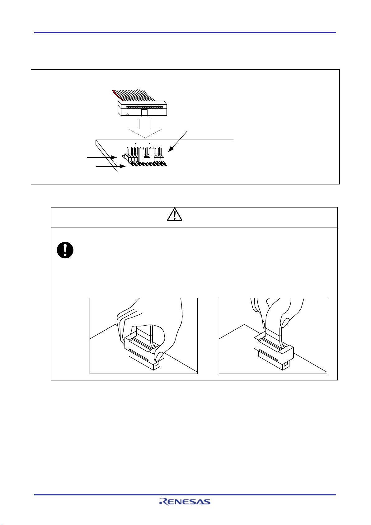
Notes on connector insertion and removal:
When connecting or disconnecting the user-system interface cable and the emulator or user system,
2.2.1 Connecting the User System Interface Cable to the 20-Pin Connector
Figure 2.1 shows how to connect the user system interface cable to the 20-pin connector.
Figure 2.1 Connecting the User System Interface Cable to the 20-Pin Connector
CAUTION
grasp the connector cover at the end of the cable. Pulling the cable itself will damage the wiring.
Also, be aware that the user-system interface cable has the direction in which it must be inserted. If
the cable is connected in the wrong direction, it may be damaged.
Correct example Incorrect example
R20UT4686EJ0100 Rev.1.00 Page 8 of 32
Mar.16.20
Page 9
E2/E2 Lite Designing the User System
Pin 2
Pin 1
FTSH-110-01-L-DV-K
Pin 2
Pin 1
FTSH-105-01-L-DV-K
Pin 2
Pin 1
FTSH-105-01-L-DV
Unit: mm
5.56 5.56
3.43 3.43
12.70
6.35
6.35
5.56
3.43
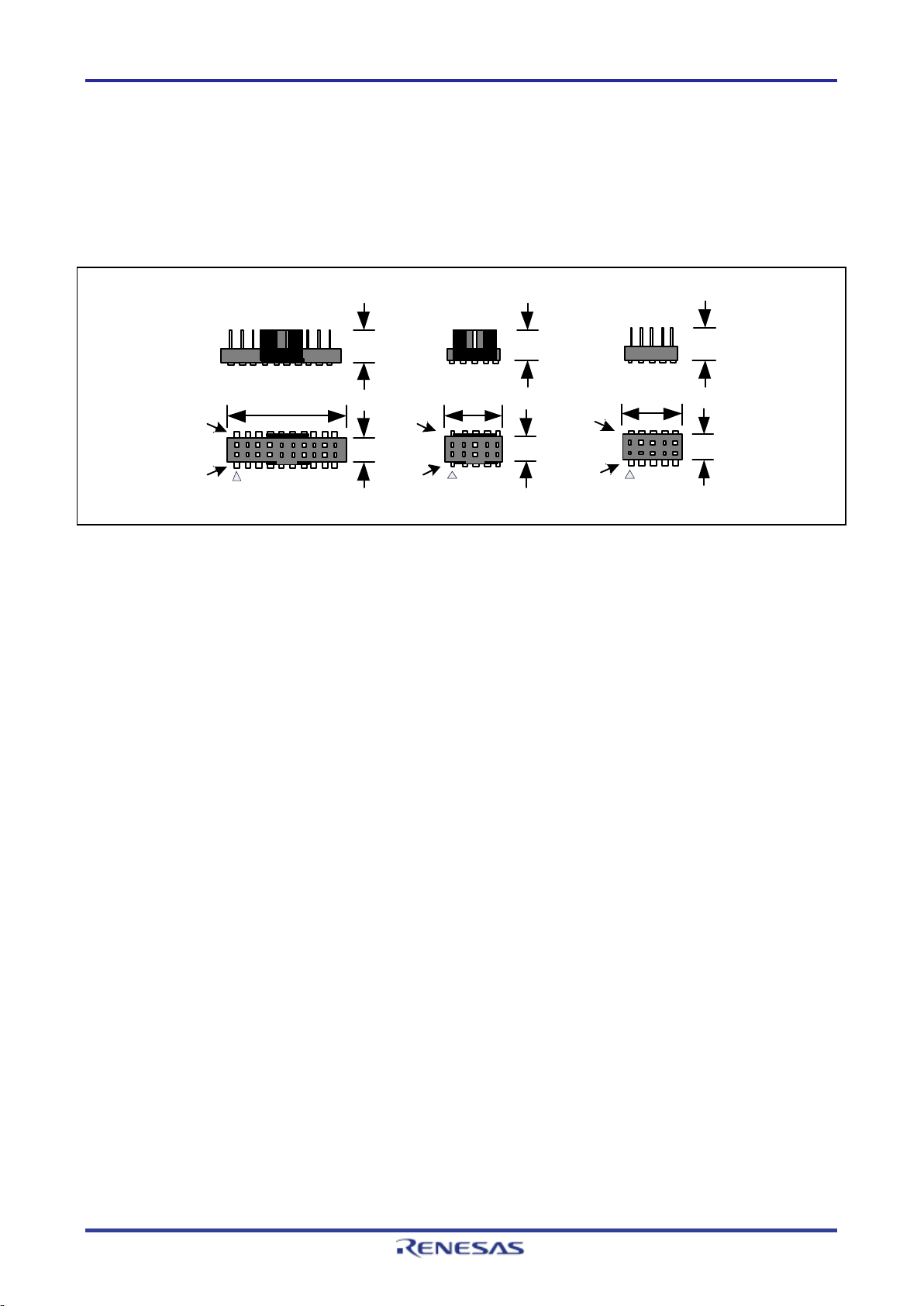
2.3 Pin Assignments of the Connector on the User System
2.3.1 20-Pin and 10-Pin Connector Specifications
Figure 2.2 shows the specifications of the 20-pin and 10-pin (1.27-mm pitch) connectors.
Table 2.3 and Table 2.4 show the pin assignments for the SWD and JTAG interface connections,
respectively.
Figure 2.2 20-Pin and 10-Pin Connector Specifications
R20UT4686EJ0100 Rev.1.00 Page 9 of 32
Mar.16.20
Page 10
E2/E2 Lite Designing the User System
Pin
1
VCC
–
Power supply
3
GND
–
MD
For setting the operating mode
6
TxD9
Output
For programming flash memory
8
RxD9
Input
For programming flash memory
10
RES#
I/O
User system reset
12*2
NC –
14*2
NC –
16*2
NC –
18*2
NC –
20*2
NC –
Table 2.3 Pin Assignments for SWD Interface Connection
No.
2 SWDIO I/O For debugging communications
4 SWCLK Input Clock for debugging communications
5 GND –
7 NC –
9 UCON – Connect this signal to ground on the user system.
11*2 NC –
13*2 NC –
15*2 GND –
Signal Direction*1 Note
It is used to confirm the connection between the
emulator and user system.
17*2 GND –
19*2 GND –
Notes: 1. Input to or output from the user system.
“Input” refers to input from the emulator to the user system and “output” refers to output
from the user system to the emulator.
2. If a 10-pin connector is mounted on the user system, pins 11 to 20 are not used.
R20UT4686EJ0100 Rev.1.00 Page 10 of 32
Mar.16.20
Page 11

E2/E2 Lite Designing the User System
Pin
1
VCC
–
Power supply
3
GND
–
MD
For setting the operating mode
6
TDO/TxD9
Output
For debugging communications and programming flash
8
TDI/RxD9
Input
For debugging communications and programming flash
10
RES
I/O
User system reset
12*2
NC –
14*2
NC –
16*2
NC –
18*2
NC –
20*2
NC –
Table 2.4 Pin Assignments for JTAG Interface Connection
No.
2 TMS Input For debugging communications
4 TCK Input Clock for debugging communications
5 GND –
7 NC –
9 UCON – Connect this signal to ground on the user system.
11*2 NC –
13*2 NC –
Signal Direction*1 Note
memory
memory
It is used to confirm the connection between the
emulator and user system.
15*2 GND –
17*2 GND –
19*2 GND –
Notes: 1. Input to or output from the user system.
“Input” refers to input from the emulator to the user system and “output” refers to output from
the user system to the emulator.
2. If a 10-pin connector is mounted on the user system, pins 11 to 20 are not used.
R20UT4686EJ0100 Rev.1.00 Page 11 of 32
Mar.16.20
Page 12

E2/E2 Lite Designing the User System
2.4 Recommended Circuit between the Connector and the MCU
This section shows recommended circuits for connection between the connector and the MCU. For details
on the handling of signals, refer to section 2.5, Notes on Connection.
R20UT4686EJ0100 Rev.1.00 Page 12 of 32
Mar.16.20
Page 13

E2/E2 Lite Designing the User System
SWCLK
SWDIO
VCC
VCC
SWCLK/MD
SWDIO
RES
GND
15, 17, 19
10
4
1
RES
VCC
Not
connected
11, 13
MCU
VCC
VCC
2
SWO/TxD9
SWO/RxD
6
RxD9
TxD
8
MD
TCLK
TDATA[0]
TDATA[1]
TDATA[2]
TDATA[3]
TCLK
12
TDATA[0]
14
TDATA[1]
16
TDATA[2]
18
TDATA[3]
20
GND
3, 5
9
UCON
7
20-pin and 10-pin
1.27-mm pitch
connector
Pull up at
4.7 kΩ to 10 kΩ
Open-collector
buffer
Reset
circuit
Not
connected
*3
*3
*1
*2
2.4.1 SWD Interface Connection
Figure 2.3 shows a recommended circuit for connection through the SWD interfaces.
Notes: 1. The MD pin can operate even if it is not connected to the emulator.
Figure 2.3 Example of Connection through the SWD Interfaces
When the MD pin is not connected to the emulator, a special circuit for the pin must be
configured on the user system. For details on handling of the MD pin, refer to section 2.5,
Notes on Connection.
2. If a 10-pin connector is mounted on the user system, pins 11 to 20 are not used.
3. The emulator does not support a trace output facility.
R20UT4686EJ0100 Rev.1.00 Page 13 of 32
Mar.16.20
Page 14

E2/E2 Lite Designing the User System
TCK
TMS
VCC
VCC
TCK/MD
TMS
RES
10
4
1
RES
VCC
VCC
VCC
2
TDO/TxD9
TDI/RxD
6
TDI/RxD9
TDO/TxD
8
MD
GND
15, 17, 19
11, 13
TCLK
TDATA[0]
TDATA[1]
TDATA[2]
TDATA[3]
TCLK
12
TDATA[0]
14
TDATA[1]
16
TDATA[2]
18
TDATA[3]
20
GND
3, 5
9
UCON
7
MCU
20-pin and 10-pin
1.27-mm pitch
connector
Pull up at
4.7 kΩ to 10 kΩ
Open-collector
buffer
Reset
circuit
Not
connected
Not
connected
*3
*1
*2
Notes:
1.
The MD pin can operate even if it is not connected to the E2 emulator.
2.
If a 10-pin connector is mounted on the user system, pins 11 to 20 are not used.
3.
The E2 emulator does not support a trace output facility.
2.4.2 JTAG Interface Connection
Figure 2.4 shows a recommended circuit for connection through the JTAG interfaces. The E2 Lite does not
support JTAG interface connection.
Figure 2.4 Example of Connection through the JTAG Interfaces
When the MD pin is not connected to the E2 emulator, a special circuit for the pin must be
configured on the user system. For details on handling of the MD pin, refer to section 2.5,
Notes on Connection.
R20UT4686EJ0100 Rev.1.00 Page 14 of 32
Mar.16.20
Page 15

E2/E2 Lite Designing the User System
- When a reset circuit is included
- When a reset circuit is not included
VCC
4.7 kΩ to 10 kΩ
RES
Connector
RES
Connector
MCU
RES
MCU
RES
4.7 kΩ to 10 kΩ
Reset
circuit
Open-collector
buffer
VCC
Do not install capacitors, series resistors, or filters on signal lines; if this is attempted, correct communication
2.5 Notes on Connection
Wiring patterns between the connector and the MCU must be as short as possible (within 50 mm is
recommended). Do not connect the signal lines between the connector and MCU to other signal lines on the
board.
For the handling of pins while the emulator is not in use, refer to the hardware manual for the MCU.
2.5.1 RES Pin
The emulator uses the RES pin.
If the user system includes a user logic reset circuit, the output signal from the reset circuit must be
connected to the RES pin of the connector via an open-collector buffer as shown below. If there is no reset
circuit, the RES pin from the connector must be directly connected to the RES pin of the MCU.
may not be established.
Figure 2.5 Connection of the RES Pin
R20UT4686EJ0100 Rev.1.00 Page 15 of 32
Mar.16.20
Page 16

E2/E2 Lite Designing the User System
MD
MD
MD
-
When an emulator is in use
Connector
MCU
- When an emulator is not in use
MCU
1.5 kΩ
Open-circuit: Single-chip mode
Short-circuit
: SCI or USB boot mode
2.5.2 MD Pin
The emulator uses the MD pin. The circuit for the MD pin of the MCU includes a pull-up resistor.
When the MD pin is to be used in SCI or USB boot mode without use of the emulator, the MD pin must be
handled so that it is switched to the low level.
Figure 2.6 Connection of the MD Pin
R20UT4686EJ0100 Rev.1.00 Page 16 of 32
Mar.16.20
Page 17
E2/E2 Lite Designing the User System
Power supply from the E2/E2 Lite depends on the quality of the USB power supply of the host machine, and as
When the MCU is changed to low power mode, the internal debugging circuit continues to run. This leads to the
WARNING
2.5.3 GND
The pins of the connector marked "GND" must be at the same ground level as the VSS pin of the MCU.
2.5.4 VCC
Connect the VCC of the connector to the VCC (power supply) of the user system.
Use the emulator within the power supply voltage of 1.8 V to 5.5 V and within the operating voltage range of
the MCU.
When power is supplied to the user system from other than the emulator, the E2/E2 Lite consumes the
power supply for the last output and first input buffers of the emulator.
• E2: 3.3 V: approximately 20 mA, 5.0 V: approximately 40 mA
• E2 Lite: 3.3 V: approximately 20 mA, 5.0 V: approximately 40 mA
The E2/E2 Lite can supply power to a simple evaluation system.
• E2: Can supply power of 1.8 V to 5.0 V, up to 200 mA.
• E2 Lite: Can supply power of 3.3 V, up to 200 mA.
When using the power supply function of the E2 or E2 Lite, check the voltage that is actually being supplied
to the user system since this depends on the environment.
such, precision is not guaranteed. When writing a program that requires reliability, do not use the power supply
function of the E2/E2 Lite. Use a stable, separate power supply for the user system. As the software when
writing a program in a mass-production process, use the Renesas Flash Programmer.
For details on the programming software, refer to the following:
Renesas Flash Programmer: https://www.renesas.com/RFP
MCU drawing more electric current than is listed in the DC characteristics of the target MCU.
Warning for Turning the Power On/Off:
When supplying power, ensure that there are no shorts between Vcc and GND. Only connect the
E2/E2 Lite after confirming that there are no mismatches of alignment on the user system port
connector. Incorrect connection will result in the host machine, the E2/E2 Lite, and the user system
emitting smoke or catching fire.
2.5.5 RxD9 and TxD9 Pins (Flash Programming via an SCI)
When flash memory is programmed via an SCI, the RxD9 and TxD9 pins must be connected to the emulator.
For MCUs in which the RxD9 and TxD9 pins can be allocated to multiple pins, check the hardware manual of
the MCU to confirm which of the pins is used in boot mode.
R20UT4686EJ0100 Rev.1.00 Page 17 of 32
Mar.16.20
Page 18
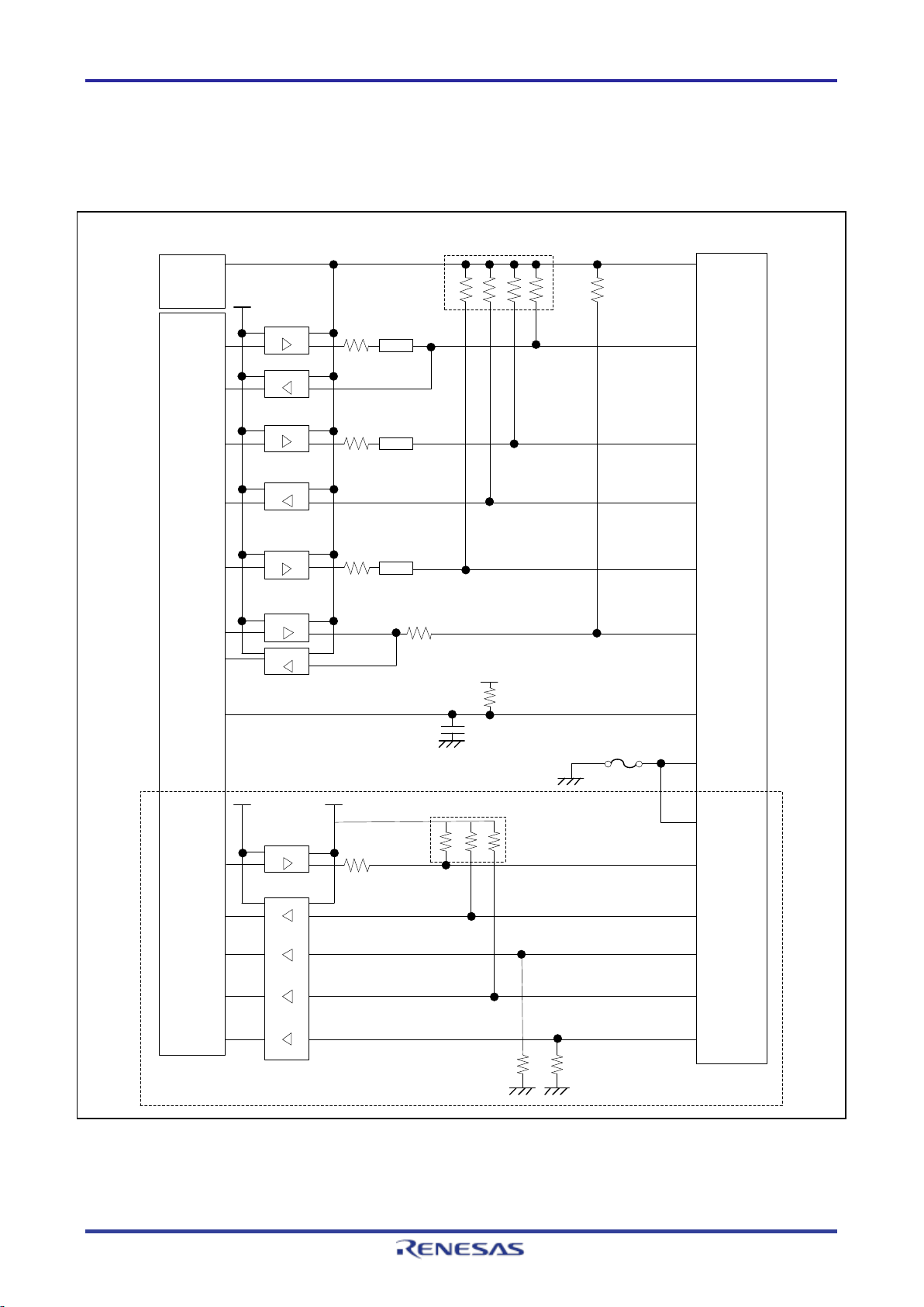
74
LVC
1T45
74LVC1T45
74LVC8T245
Emulator
control
circuit
NFL21SP
VCC
SWCLK/TCK/MD
1
4
2
SWDIO/TMS
9
10
3, 5
GND
UCON
RES
3.3 V
74LVC1T45
74LVC1T45
0.1 uF
NFL21SP
74LVC8T245
TDO/TxD
8
6
SWO/TDI/RxD
74LVC1T45
NFL21SP
GND 15, 17, 19
3.3 V
VCC
1 MΩ
74LVC1T45
12
TCLK
74LVC8T245
14
TDATA[0]
16
TDATA[1]
18
TDATA[2]
20
TDATA[3]
3 MΩ
*1
3.3 V
47 Ω
Noise filter
1 MΩ x 4
Power-supply
circuit
(only for use in
the mode to
supply power to
the user system)
User-side
connector
100 kΩ
47 Ω
Noise filter
47 Ω
Noise filter
47 Ω
47 Ω
100 kΩ
1 MΩ x 3
Self-recovering
fuse
E2/E2 Lite Designing the User System
2.6 Internal Circuits of the Emulator
2.6.1 Internal Circuits of the E2
Figure 2.7 shows the internal circuits of the E2.
Figure 2.7 Internal Circuits of the E2
Note 1: If a 10-pin connector is mounted on the user system, pins 11 to 20 are not used.
R20UT4686EJ0100 Rev.1.00 Page 18 of 32
Mar.16.20
Page 19

E2/E2 Lite Designing the User System
74LVC125
74LVC8T245
74LVC125
3.3 V
Emulator
control
circuit
74LVC8T245
3.3 V
VCC
1
2
4
9
10
3, 5,
15, 17,
19
GND
100 kΩ
SWCLK/MD
UCON
RES
SWDIO
74LVC125
6
SWO/RxD
74LVC125
8
TxD
74LVC8T245
47 Ω
100 kΩ x 5
Power-supply
circuit
(only for use in
the mode to
supply power to
the user system)
User-side
connector
47 Ω
47 Ω
47 Ω
47 Ω
47 Ω
Self-recovering
fuse
2.6.2 Internal Circuits of the E2 Lite
Figure 2.8 shows the internal circuits of the E2 Lite.
Figure 2.8 Internal Circuits of the E2 Lite
R20UT4686EJ0100 Rev.1.00 Page 19 of 32
Mar.16.20
Page 20

E2/E2 Lite Notes on Usage
CAUTION
3. Notes on Usage
3.1 Turning the Power On/Off
Turn the power of the emulator and the user system following the procedure below.
3.1.1 When a Separate Power Supply is Used for the User System
<When using the emulator>
(1) Check that the power is off.
(2) Connect the user system.
Connect the emulator and the user system with a user-system interface cable.
(3) Connect the host machine and turn on the emulator.
Connect the emulator and the host machine with a USB interface cable. The E2/E2 Lite is turned on by
connecting the USB interface cable.
(4) Launch the emulator debugger or programming software.
Launch the emulator debugger or programming software.
(5) Turn on the user system.
Turn on the user system.
(6) Connect the emulator debugger or programming software to the emulator.
Connections may vary depending on software.
<When finished using the emulator>
(1) Disconnect the emulator from the emulator debugger or programming software.
Disconnections may vary depending on software.
(2) Turn off the user system.
Turn off the user system.
(3) Close the emulator debugger or programming software.
Close the emulator debugger or programming software.
(4) Turn off the emulator and disconnect the emulator.
Disconnect the USB interface cable from the emulator. The E2/E2 Lite is turned off by disconnecting from
the USB interface cable.
(5) Disconnect the user system.
Disconnect the user-system interface cable from the user system.
Notes on the User System Power Supply:
While the power of the user system is on, do not turn off the host machine or unplug the USB
interface cable.
The user system may be damaged due to leakages current.
R20UT4686EJ0100 Rev.1.00 Page 20 of 32
Mar.16.20
Page 21

E2/E2 Lite Notes on Usage
3.1.2 When Power is Supplied to the User System from the Emulator
<When using the emulator>
(1) Connect the user system.
Connect the emulator and the user system with a user-system interface cable.
(2) Connect the host machine and turn on the emulator.
Connect the emulator and the host machine with a USB interface cable, then turn on the emulator.
(3) Launch the emulator debugger.
Launch the emulator debugger and select the setting of power supply to the user system.
Under [Power] on the [Connection Settings] tabbed page, select [Yes] for [Power Target From The
Emulator (MAX 200mA)]. Refer to section 3.3, Notes on Using the Emulator Debugger, for how to open
the [Debug Configurations] window.
Figure 3.1 Setting for Supplying Power
(4) Connect the emulator debugger or programming software to the emulator.
Connections may vary depending on software.
<When finished using the emulator>
(1) Disconnect the emulator from the emulator debugger or programming software.
Disconnections may vary depending on software.
(2) Close the emulator debugger or programming software.
Close the emulator debugger or programming software.
(3) Turn off the emulator and disconnect the emulator.
Disconnect the USB interface cable from the emulator, then turn off the emulator.
(4) Disconnect the user system.
Disconnect the user-system interface cable from the user system.
3.2 Power Supply Function of the E2/E2 Lite
The E2/E2 Lite can supply power to a simple evaluation system.
• E2: Can supply power of 1.8 V to 5.0 V, up to 200 mA.
• E2 Lite: Can supply power of 3.3 V, up to 200 mA.
When using the power supply function of the E2 or E2 Lite, check the voltage that is actually being supplied
to the user system since this depends on the environment.
R20UT4686EJ0100 Rev.1.00 Page 21 of 32
Mar.16.20
Page 22

E2/E2 Lite Notes on Usage
3.3 Notes on Using the Emulator Debugger
This section describes how to set the [Debug Configurations] window of the e2 studio. To open the [Debug
Configurations] window, click on [Run] → [Debug Configurations…] or the downward-pointing arrow next to
the icon→ [Debug Configurations…].
Figure 3.2 Opening the [Debug Configurations] Window
Figure 3.3 [Debug Configurations] Window
R20UT4686EJ0100 Rev.1.00 Page 22 of 32
Mar.16.20
Page 23

E2/E2 Lite Notes on Usage
For example, when the following values have been secured, enter 00112233445566778899aabbccddeeff.
const unsigned long __OSISreg[4] = {
0x33221100,
0x77665544,
0xbbaa9988,
0xffeeddcc
};
3.3.1 Notes on Connecting the Emulator Debugger
(1) Reset state
Under [Connection] on the [Connection Settings] tabbed page, be sure to select [Yes] for [Hold reset
during connect].
When [Yes] is selected, during connection to the emulator debugger, the emulator maintains the low-level
output on the RES# pin of the MCU and places the MCU in the OCD mode. However, to start the
operation of the built-in debugging circuits of the MCU, the emulator releases the reset for about 50 msec
while it is connected, and the user program automatically runs during that period.
Figure 3.4 Setting of [Hold reset during connect]
(2) Startup mode
When the emulator debugger is connected, handle the pins on the user system so that the startup mode
of the MCU is single-chip mode.
In single-chip mode, the MD pin is at the high level. Correct connection of the emulator debugger is not
possible in SCI/USB boot mode.
(3) Debugging after rewriting ID code
If the ID code (OSIS register) has been rewritten, enter the new ID code.
Here, the ID code to be entered means the value to be entered in [ID Code (Bytes)] under [Connection]
on the [Connection Settings] tabbed page.
Figure 3.5 Setting of [ID Code (Bytes)]
R20UT4686EJ0100 Rev.1.00 Page 23 of 32
Mar.16.20
Page 24

E2/E2 Lite Notes on Usage
(4) Entering the ALeRASE command for ID code
If an ALeRASE command is entered in [ID Code (Bytes)] under [Connection] on the [Connection Settings]
tabbed page, the code flash memory and option-setting memory will be erased when the emulator
debugger is connected.
For the conditions under which the ALeRASE command is usable, refer to the hardware manual for the
MCU you are using. If the ALeRASE command is entered then the emulator debugger is connected while
the command is not usable on the MCU, an error message “Failed to erase all flash memory by the ID for
erasing all flash memory.” is displayed and the connection process is suspended.
3.3.2 Notes on a Debugging Operation that Involves Reprogramming of Flash Memory
A “debugging operation that involves reprogramming of flash memory” refers to the following operations of
the emulator debugger.
• Downloading data to flash memory
• Using software break functions in flash memory
(a) Setting and canceling breakpoints
(b) Executing or step-executing programs from a breakpoint
(c) Using the “Run to Line” function from the state where a break was set
(1) Program for reprogramming flash memory
Since the emulator debugger enables a debugging operation that involves reprogramming of flash
memory, the emulator writes the program for reprogramming flash memory to the on-chip SRAM and
executes the program to reprogram the flash memory. After the flash memory has been reprogrammed,
the emulator debugger restores the on-chip SRAM to its initial state.
(2) Destination for allocation of the program for reprogramming flash memory
By default, the program for reprogramming the flash memory is allocated to the 5-Kbyte space from the
address where the SRAM0 area starts (or the address where the SRAMHS area starts for devices that do
not include an SRAM0 area). If the default allocation destination is not available due to the security
settings or DMAC/DTC transfer*, enter the start address of an available space in the on-chip RAM in units
of 1000h bytes against [Work RAM Start Address] under [Flash] on the [Debug Tool Settings] tabbed
page for the emulator debugger.
Note: The DMAC or DTC will continue to operate even during a break. Take care that a transfer source or
destination for the DMAC or DTC is not within the address range of the working RAM where the
program is to be allocated.
Figure 3.6 Setting of [Work RAM Start Address]
R20UT4686EJ0100 Rev.1.00 Page 24 of 32
Mar.16.20
Page 25

E2/E2 Lite Notes on Usage
(3) Interrupts and resets during execution of the program for reprogramming flash memory
Interrupts other than non-maskable interrupts are to be masked while the program for reprogramming
flash memory is being executed. Also, so that the program for reprogramming flash memory is correctly
executed, all interrupt source flags which have been set before executing the program are cleared.
If a non-maskable interrupt occurs, the emulator continues running the program for reprogramming flash
memory. If a reset occurs while the program for reprogramming flash memory is being executed, the
emulator shows an error message and stops processing. Since doing so may damage the contents of
flash memory, do not apply a reset while the program is running.
(4) Conditions for downloading data to flash memory being available
When the MCU satisfies all the following conditions, the downloading of data to flash memory can
proceed.
(a) The code flash memory of the MCU is in read mode.
(b) The frequency of the system clock (ICLK) of the MCU is 1 MHz or higher.*
Note: For [Clock] in the [Connection Settings] tabbed page of the emulator debugger, when [Yes] is
selected for [Permit Clock Source change on writing on-chip Flash Memory], condition (b) can be
excluded.
Figure 3.7 Setting of [Permit Clock Source change on writing on-chip Flash Memory]
If data are downloaded to flash memory while any condition is not satisfied, the emulator shows an error
message and stops processing. In such a case, restart downloading of data to flash memory after the CPU
has been reset or reconnect the emulator debugger after reviewing its settings.
(5) Downloading data to a secure area
When downloading data to a secure area which has been specified for the security MPU, for [Flash] in the
[Debug Tool Settings] tabbed page of the emulator debugger, select [Yes] for [Erase on-chip program
flash before download].
Figure 3.8 Setting of [Erase on-chip program flash before download]
(6) Access window function
When the access window function of the MCU is to be used, only reprogram the flash memory in the area
specified for access.
R20UT4686EJ0100 Rev.1.00 Page 25 of 32
Mar.16.20
Page 26

E2/E2 Lite Notes on Usage
(7) Conditions for using software breaks in flash memory
When the MCU satisfies all the following conditions, the software break function for flash memory is
enabled.
(a) The code flash memory of the MCU is in read mode.
(b) The frequency of the system clock (ICLK) of the MCU is 1 MHz or higher.*
(c) For [Break] in the [Debug Tool Settings] tabbed page, [Yes] is selected for [Use Flash Breakpoints].
Figure 3.9 Setting of [Use Flash Breakpoints]
Note: For [Clock] in the [Connection Settings] tabbed page of the emulator debugger, when [Yes] is
selected for [Permit Clock Source change on writing on-chip Flash Memory], condition (b) can be
excluded.
Figure 3.10 Setting of [Permit Clock Source change on writing on-chip Flash Memory]
If the software break function is used with any condition not satisfied, the emulator shows an error message.
In such a case, use the hardware break or confirm that conditions (a) to (c) above are satisfied.
(8) Flash memory I/O register
After a debugging operation that involves reprogramming of flash memory, the value of the flash memory
I/O register is rewritten by the emulator debugger.
3.3.3 Note on Using Software Breaks in the On-Chip SRAM
(1) Overwriting of software breakpoints by user programs
If a software breakpoint is overwritten by a user program, the program will not stop even if it runs through
the address. In such a case, set the software breakpoint after the target on-chip SRAM has been
rewritten by the program.
R20UT4686EJ0100 Rev.1.00 Page 26 of 32
Mar.16.20
Page 27

E2/E2 Lite Notes on Usage
3.3.4 Notes on Using Software Breaks (Common to the On-Chip SRAM and Flash Memory)
(1) Setting software breakpoints in a secure area
Do not set software breakpoints in a secure area which has been specified by the security MPU. If this is
attempted, an instruction code may be restored as incorrect data on release of the break.
(2) Reading an address where a software breakpoint has been set
Do not read an address where a user program has set a software breakpoint. Doing so may cause the
program to operate in a different way from in the normal state.
(3) Viewing memory in the [Memory] view
During execution of the user program, if a range of memory in which a software breakpoint has been set
is displayed in the [Memory] view of the emulator debugger, the value (BKPT instruction code) that is
shown is different from that in the actual program data.
(4) Removal of software breakpoints when the emulator debugger is to be disconnected
When the emulator debugger is to be disconnected, remove all software breakpoints that have been set.
At this time, reset the CPU since the emulator debugger is certain to reprogram the flash memory.
3.3.5 Note on Peripheral I/O Registers Occupied by the Debugger
(1) Peripheral I/O registers occupied by the debugger
The emulator debugger occupies the following peripheral I/O registers during debugging. Do not change
the values of these registers, since continued debugging might not be possible after having done so.
Debug stop control register (DBGSTOPCR)
Micro trace buffer (MTB) (SFR area)
System control OCD control register (SYOCDCR)
3.3.6 Note on Using the Trace Function
(1) MTB tracing
When the MTB trace function is in use, the trace recording area is the size of recorded tracing that has
been selected for the emulator debugger from the address where the on-chip SRAM starts. When the onchip SRAM is in use by a user program, do not use the trace recording area. For details on the address
where the on-chip SRAM starts, refer to the hardware manual for the given MCU.
If the size of the trace recording area for the emulator debugger is changed, the startup routine must also
be changed.
R20UT4686EJ0100 Rev.1.00 Page 27 of 32
Mar.16.20
Page 28
E2/E2 Lite Notes on Usage
3.3.7 Notes on Low-Power Modes
(1) Debugging in SSTBY or SNOOZE mode
In SSTBY or SNOOZE mode, the emulator debugger does not have access to the system bus of the
MCU. While the user program is being executed or during mode transitions of the MCU, setting and
viewing of the memory or peripheral I/O registers and setting and changing breakpoints are not possible.
(2) Forcedly stopping a program in SSTBY or SNOOZE mode
When a program is forcedly stopped in SSTBY or SNOOZE mode, proceed with one of the following
operations. Each operation leads to release from SSTBY or SNOOZE mode.
Using [Reset ] of the emulator debugger makes the MCU stop the user program and go to the
position indicated by the reset vector.
Using [Suspend ] of the emulator debugger stops the MCU at the next instruction after the WFE
instruction which led to the mode transition. When [Suspend ] is to be used, for [Connection] on
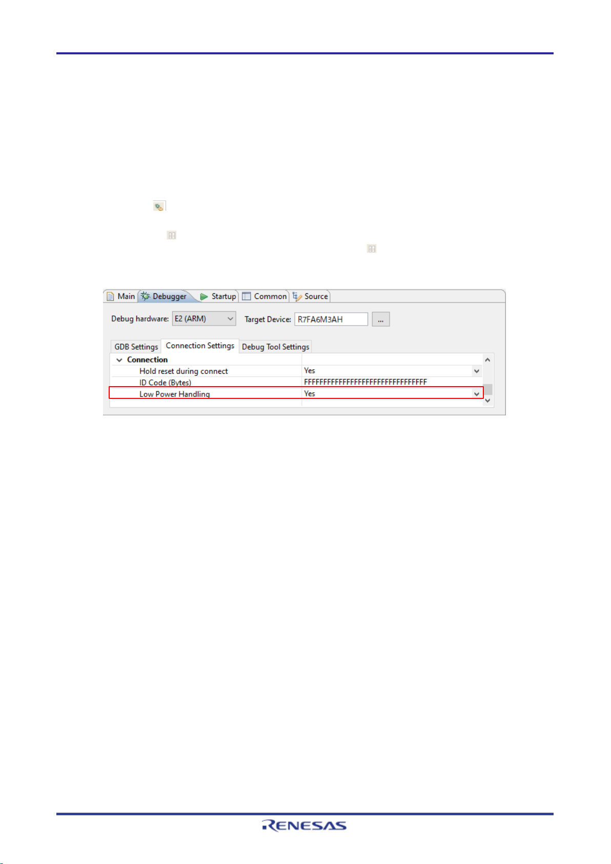
the [Connection Settings] tabbed page of the emulator debugger, select [Yes] for [Low Power
Handling].
Figure 3.11 Setting of [Low Power Handling]
(3) Debugging in DSTBY mode
Debugging a program that has entered DSTBY is not supported.
3.3.8 Current Drawn during Debugging
Since the debugging circuits within the MCU are always active during connection of the emulator debugger,
the MCU draws more current than in the actual user system. Take care on this point when attempting to
measure the current drawn in the user system.
R20UT4686EJ0100 Rev.1.00 Page 28 of 32
Mar.16.20
Page 29

E2/E2 Lite Notes on Usage
Arm MPU
Accessible
Slave MPU
Accessible
3.3.9 Note on the Memory Protection Units (MPUs)
(1) Access to protected areas
Table 3.1 shows the operation of the emulator debugger in response to attempted access to areas
protected by each of the MPUs.
Table 3.1 Access to MPU-Protected Areas
Protected Area Operation of the Emulator Debugger
Bus master MPU The protected area is not accessible.
Security MPU On-chip SRAM/peripheral I/O registers
• Reading: A dummy value (0x00) is read.
• Writing: Writing is ignored.
Flash memory
• Reading: A dummy value (0x00) is read.
• Writing: Writing is possible if data are downloaded and written.
3.4 MCUs that are Used in Debugging
After debugging with the emulator, if the MCU is disconnected from the emulator and run on its own, correct
operation cannot be guaranteed. To operate the MCU on its own, use the programming software to reprogram the MCU.
MCUs that are connected to the emulator and used in debugging are placed under stress by repeated
programming of flash memory during emulation. Do not use MCUs that were used in debugging in massproduction for end users.
3.5 Final Evaluation of the User Program
Before entering the mass-production phase, be sure to perform a final evaluation of the program which has
been written to the flash ROM by the programming software, without the emulator connected.
R20UT4686EJ0100 Rev.1.00 Page 29 of 32
Mar.16.20
Page 30

Rev.
Date
Description
Page
Summary
1.00
Mar.16.20
E2 Emulator, E2 Emulator Lite
Revision History
Additional Document for User's Manual
(Notes on Connection of RA Devices)
Page 31

Published by: Renesas Electronics Corporation
E2 Emulator, E2 Emulator Lite
Additional Document for User's Manual
(Notes on Connection of RA Devices)
Publication Date: Rev.1.00 Mar.16.20
Page 32

00
E2 Emulator, E2 Emulator Lite
Additional Document for User's Manual
(Notes on Connection of RA Devices)
R20UT4686EJ01
 Loading...