

Page 1
Cover
E1/E20 Emulator, E2 Emulator
Rev.3.00 Oct 2020
Supported Devices:
RH850 Family RH850/E1x Series
All information contained in these materials, including products and product specifications,
website (http://www.renesas.com).
Additional Document for User’s Manual
(Notes on Connection of RH850/E1M-S2)
represents information on the product at the time of publication and is subject to change by
Renesas Electronics Corp. without notice. Please review the latest information published by
Renesas Electronics Corp. through various means, including the Renesas Electronics Corp.
Page 2

Notice
on of
1. Descriptions of circuits, software and other related information in this document are provided only to illustrate the operati
semiconductor products and application examples. You are fully responsible for the incorporation or any other use of the circuits,
software, and i nformation i n the desi gn of your produc t or syste m. Renesa s Electr onics discla ims any and al l liabilit y for any loss es and
damages incurred by you or third parties arising from the us e of these circuits, software, or information.
2. Renesas Elec tronics hereby expressly disclaims any warranties against and li ability for infr ingement or any other claims involving patents,
copyrights, or other intellectual prop erty rights of third part ies, by or arising from the use of Renesas Electronics pr oducts or technical
information described in this document, including but not limited to, the product data, drawings, charts, programs, algorithms, and
application examples.
3. No license, expr ess, impli ed or otherwi se, is gra nted hereb y under an y patents , copyright s or other intell ectual prop erty rights of Renesas
Electronics or others.
4. You shall not alter , modify, copy, or revers e engineer any Renes as Electr onics product , whether in whole or in part. Renesas Electronics
disclaims any and all liability for any losses or damages incurred by you or third parties arising from such alteration, modification,
copying or reverse engineering.
5. Renesas Electroni cs products are cla ssified accordi ng to the following two qua lity grades: “Sta ndard” and “High Quali ty”. The intended
applications for each Renesas E lectronics product depends on the product’s quality grade, as indicated below.
“Standard”: Computers; office equipment; c ommunications equipment; test and measurement equipment; audio and visual equipment;
home electronic appliances; mac hine tools; personal electronic equipment; industrial robots; etc .
“High Quality”: Transportation equipment (automobiles, trains, ships, etc.); traffic control (traffic lights); large-scale communication
equipment; key financial terminal systems; safety control equipment; etc.
Unless expressl y designated a s a high reli abilit y product or a product for ha rsh environ ments in a Renes as Elec tronics data sheet or ot her
Renesas Electr onic s docum ent, Ren esa s El ectr onic s pr oduc ts a re not i ntended or a uthor i z ed for us e in produc t s or systems tha t may pose a
direct threat to huma n life or bodily injury (ar tificial life supp ort devices or systems; s urgical implantations ; etc.), or may cause ser ious
property damage (s pace system; unders ea repeaters ; nuclear power cont rol systems; a ircraft control systems; key pla nt systems; milit ary
equipment; etc. ). Renesa s El ectroni cs dis claims a ny and al l liab ilit y for any damages or los ses i ncurred b y you or any thi rd parties arising
from the use of any Renes as Electronics product that is inconsistent with any Renesa s Electronics data sheet, us er’s manual or other
Renesas Electronics document.
6. When using Renesas Elect roni cs product s, r efer to t he lates t product informa tion ( data sheet s, user ’s manu als, applica tion not es, “Genera l
Notes for Handling a nd Using Semic onductor Devices ” in the relia bility handbook, etc.), and ens ure that usage c onditions are w ithin the
ranges specified by Renesas Electronics with respect to maximum ratings, operating power supply voltage range, heat dissipation
characterist ics, insta llation, etc. Renesa s Electr onics dis claims any and a ll liabi lity for any ma lfunct ions, fa ilure or acc ident aris ing out of
the use of Renesas Electronics products outside of such specified ranges.
7. Although Renesa s Electroni cs endeavors to imp rove the qual ity and relia bility of Renes as Electroni cs products, semiconductor products
have specific cha racteristics, such as the occurrenc e of failure at a certain rate and malf unctions under certain use conditi ons. Unless
designated as a high reliability product or a product for harsh environments in a Renesas Electronics data sheet or other Renesas
Electronics document, Renesa s Elect ronics produc ts are not s ubject t o radiation res istance des ign. You are r esponsib le for implement ing
safety measures to gua rd aga ins t the pos sibi lity of b odil y injur y, injur y or da mage c aus ed by fir e, a nd/or d anger t o the p ublic in the e vent
of a failure or malf unction of Renesas Elec tronics pr oducts, s uch as safety design for hardware a nd software, including b ut not limit ed to
redundancy, fire control and malfunction prevention, appropriate treatment for aging degradation or any other appropriate measures.
Because the e valuat ion of mic roc omputer s oft ware a lone is very dif fi cult and imp ract ical, you are res pons ibl e for eval uat ing the s afet y of
the final products or systems manufactured by you.
8. Please contact a Renesas El ectronics sa les office f or details as to environmenta l matters such as the en vironmental compatibility of each
Renesas Elec tronic s produc t. Y ou are r esp onsibl e for c aref ully and s uff icient ly inves ti gati ng appl icab le laws and r egulat ions that regula te
the inclusion or use of controlled substances, including without limitation, the EU RoHS Directive, and using Renesas Electronics
products in compl iance with all these applicab le laws and regul ations. Renesa s Electr onics disclai ms any and all liab ility for damages or
losses occurring as a result of your nonc ompliance with applicable laws and regulations.
9. Renesas Electr oni cs pr oduc ts and t echnol ogi es s ha ll not be us ed f or or incorp or ated i nt o any pr oduc ts or s ystems whos e manuf act ur e, us e,
or sale is pr ohibited under a ny applica ble domestic or foreign laws or regulati ons. You shall comply with an y applicabl e export contr ol
laws and regulations promulgated and administered by the governments of any countries asserting jurisdiction over the parties or
transactions.
10. It is the respons ibility of the buyer or distributor of Renesas Electronics products, or any other party who dist ributes, disposes of, or
otherwise sell s or tr ansf er s the p r oduct to a thi rd pa r ty, t o noti f y such t hir d p ar ty in a dvanc e of the c ont ent s a nd condi t ions s et f orth i n t his
document.
11. This document sha ll not be repri nted, rep roduced or dup licated i n any form, in whole or in part, wit hout prior wr itten consent of Renesa s
Electronics.
12. Please contact a Renesas Electronics sales of fice if you have any q uestions regarding the information contained in this document or
Renesas Electronics products .
(Note 1) “Renesas Electronics” as used in this doc ument means Re nesas Electr onics Corpora tion and als o includes it s directly or indi rectly
controlled subsidiaries.
(Note 2) “Renesas Electronics product(s)” means any product developed or manufactured by or for Renesas Electronics.
(Rev.4.0-1 November 2017)
Page 3

E1/E20/E2 Emulator Contents
Contents
Table of contents
1. Outline .................................................................................................................................................................................................. 4
1.1 Features of an E1, E20 or E2 emulator ........................................................................................................................................ 4
1.2 Caution on using the E20 emulator .............................................................................................................................................. 4
1.3 Configuration of manuals .............................................................................................................................................................. 4
2. Connecting the Emulator and User System ......................................................................................................................................... 5
2.1 Connector mounted on the user system ....................................................................................................................................... 5
2.2 Pin assignments of the connector ................................................................................................................................................ 7
2.3 Connection interface and modes .................................................................................................................................................. 8
2.4 Examples of recommended connections between the connector and MCU ................................................................................ 9
2.4.1 Example of recommended connections ................................................................................................................................. 9
2.4.2 Connecting the RESET pin .................................................................................................................................................. 12
2.4.3 Connecting the TVDD pin .................................................................................................................................................... 13
2.4.4 Hot plug-in adapter for the E1 emulator ............................................................................................................................... 14
2.4.5 Isolator for the E1 emulator .................................................................................................................................................. 14
2.4.6 Small connector conversion adapter for the E1 emulator .................................................................................................... 14
3. Specifications ..................................................................................................................................................................................... 15
3.1 Overview of specifications specific to the E2 emulator............................................................................................................... 20
3.1.1 Software tracing (LPD output) .............................................................................................................................................. 20
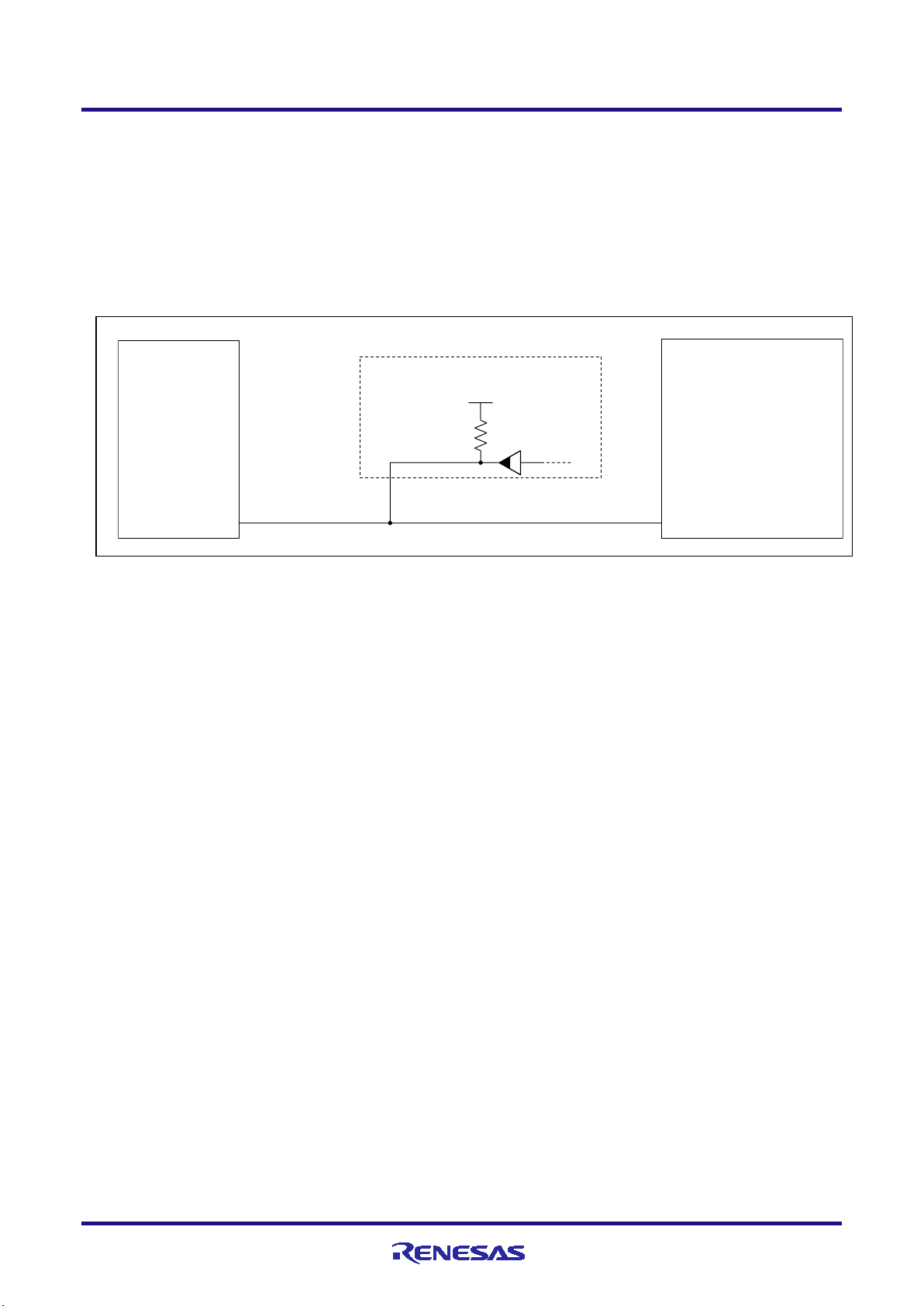
3.1.2 External trigger input and output .......................................................................................................................................... 21
4. Notes on Usage ................................................................................................................................................................................. 22
4.1 Notes on differences in operation between the actual device and the E1, E20 or E2 emulator ................................................. 22
4.2 Cautionary notes on debugging .................................................................................................................................................. 24
5. Internal Circuits of the Emulator ......................................................................................................................................................... 36
6. Troubleshooting ................................................................................................................................................................................. 38
6.1 Problems when the emulator is connected ................................................................................................................................. 38
6.2 Problems after the emulator is connected .................................................................................................................................. 40
R20UT3433EJ0300 Rev.3.00 Page 3 of 44
Oct.09.20
Page 4

E1/E20/E2 Emulator 1. Outline
1. Outline
1.1 Features of an E1, E20 or E2 emulator
An E1, E20 or E2 emulator is an on-chip debugging emulator that includes a flash programming function, which is used
for debugging and programming programs to be embedded in microcontrollers that have on-chip flash memory. That is,
either product can debug a program while the target microcontroller is connected to the user system, and can write
programs to the on-chip flash memory of microcontrollers.
1.2 Caution on using the E20 emulator
The functions used for debugging of the RH850 family by using the E20 emulator are the same as in the E1 emulator.
Large trace function, characteristic function of the E20 emulator, cannot be used.
1.3 Configuration of manuals
When using the E1, E20 or E2 emulator in debugging with an RH850 family product, be sure to read the manuals (1) and
(2) below. Also read the application note (3) if required.
(1) E1 or E20 emulator user’s manual, E2 emulator user’s manual
The E1/E20 Emulator User’s Manual, E2 Emulator User’s Manual describes hardware specifications including the
following items:
• Components of the emulators
• Emulator hardware specifications
• Connecting the emulator to a host computer and user system
(2) E1 or E20 emulator, E2 emulator additional document for user’s manual
An E1 or E20 Emulator, E2 Emulator Additional Document for User’s Manual describes functions of a debugger,
and its contents depend on the given set of MCUs. In general, an additional document has notes on items including
the following:
• For use in hardware design, an example of connection and the interface circuits required to connect the
emulator.
• Notes on using the emulator
(3) E2 emulator application note
The E2 Emulator Application Note includes an explanation, descriptions of usage, and notes on the extended
functions of the E2 emulator.
R20UT3433EJ0300 Rev.3.00 Page 4 of 44
Oct.09.20
Page 5
E1/E20/E2 Emulator 2. Connecting the Emulator and User System
Type
Manufacturer
Specification
2514-6002
3M Limited
14-pin straight type (other countries)
12
11 13
14
910785
6
341
2
5 mm
5 mm
5 mm 5 mm
Top View
Area where restriction applies to mounted components
(components must have heights no greater than 10 mm)
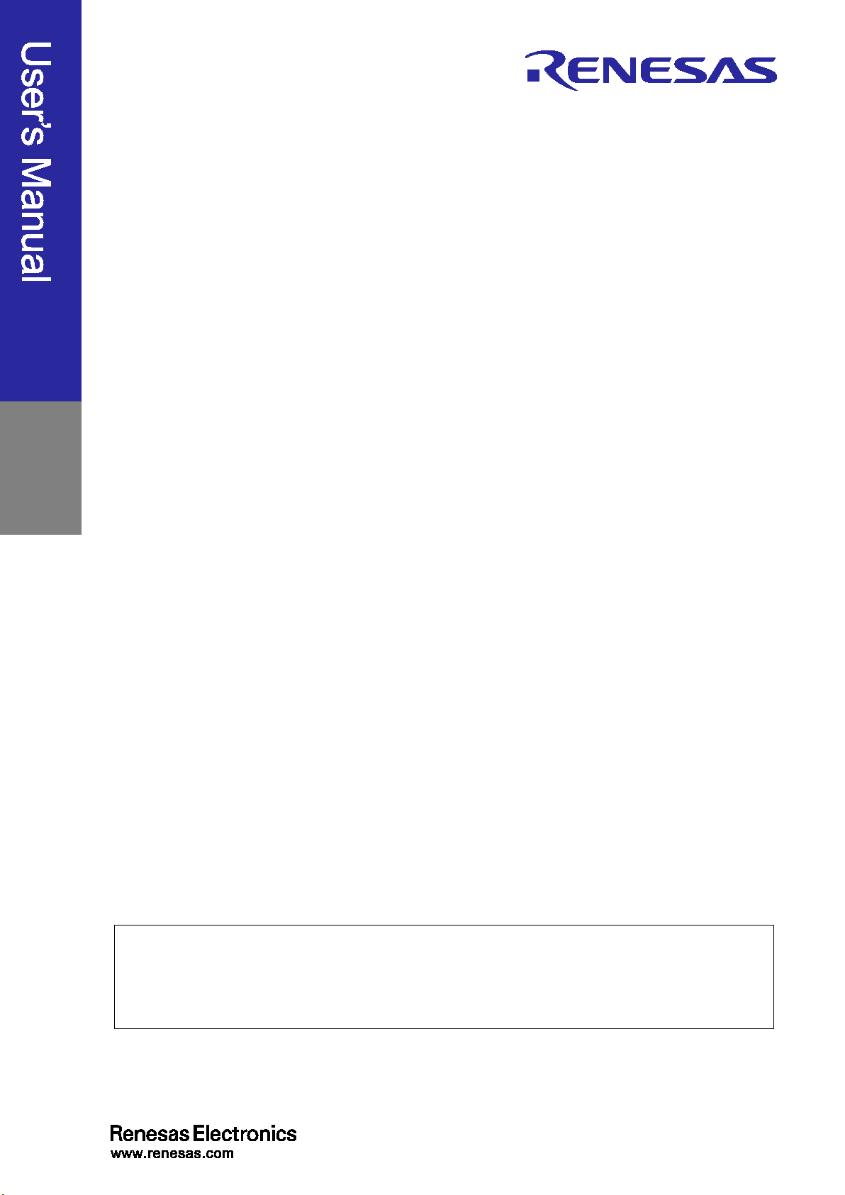
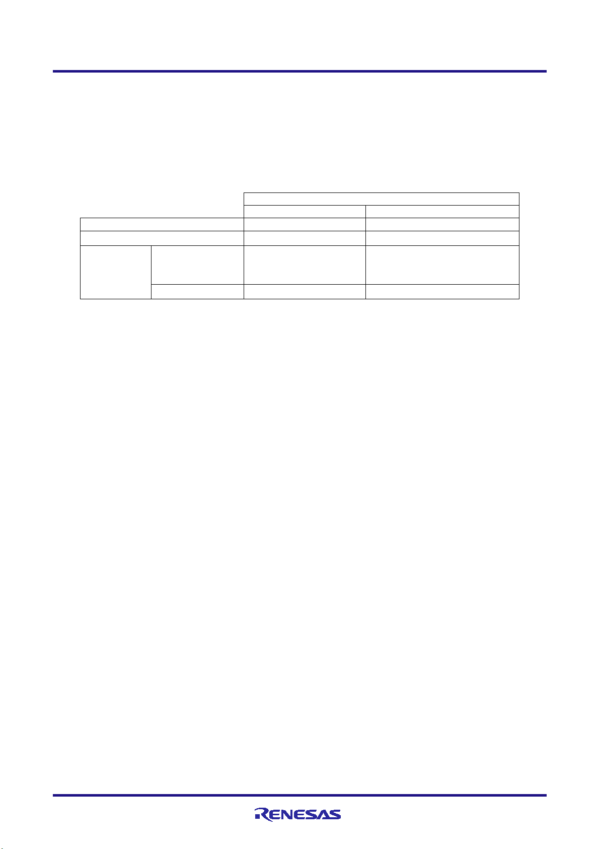
2. Connecting the Emulator and User System
To connect the E1, E20 or E2 emulator, a connector for the user system interface cable must be mounted on the user
system. When designing the user system, read this chapter of this manual and the hardware manual for the MCUs to be
used.
2.1 Connector mounted on the user system
Table 2-1 shows the recommended connectors for connection of the E1, E20 or E2 emulator. If you intend to use the 14-
pin connector, do not mount components with heights exceeding 10 mm within 5 mm of the connector on the user system
as shown in Figure 2-1.
Table 2-1 Recommended Connectors
Number
14-pin
connector
7614-6002 3M Japan Limited 14-pin straight type (Japan)
Figure 2-1 Area where Restriction Applies to Mounted Components
• For the connection of an E1 emulator
Figure 2-2 shows an example of the connection of the user system interface cable of an E1 emulator to a 14-pin connector.
Figure 2-2 Connecting the User System Interface Cable to the 14-pin Connector in the E1 Emulator
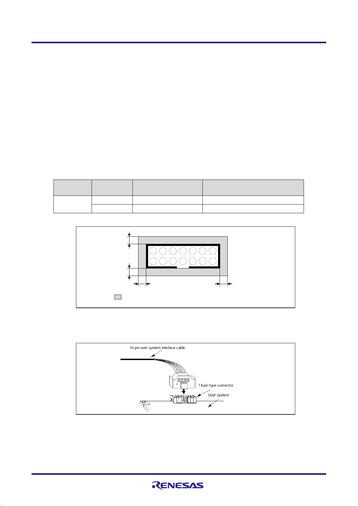
• For the connection of an E20 emulator
To use an E20 emulator with a 14-pin connector, use the 38-pin/14-pin connector conversion adapter
[R0E000200CKA00] that comes with the E20.
R20UT3433EJ0300 Rev.3.00 Page 5 of 44
Oct.09.20
Page 6
E1/E20/E2 Emulator 2. Connecting the Emulator and User System
20
-pin (1.27-mm pitch) connector
user-system interface cable
13 mm
10.5 mm
User system
Connector for the emulator:
14-pin (2.54-mm pitch)
connector
7614-6002 or 2514-6002
20-pin (1.27-mm pitch)
to 14-pin (2.54-mm
pitch) connector
conversion adapter
10.5 mm
20-pin (1.27-mm pitch) to 14-pin (2.54-mm
pitch) connector conversion adapter (top
view)
29
.0 mm
1
3
Set the switch on the “1” side
when the target device is an
RH850 and on the “3” side when
the target device is an RL78.
Setting
Description
1
The target device is an RH850 microcontroller (default setting).
CAUTION
Note on connector insertion and removal (1):
damage the wiring.
CAUTION
Note on connector insertion and removal (2):
Be aware that the user-system interface cable or the connector conversion adapter must be inserted with the correct
the wrong
orientation may cause damage.
• For the connection of an E2 emulator
To use an E2 emulator with a 14-pin connector, use the connector conversion adapter that comes with the E2. Figure 2-3
shows an example of the connection.
The connector conversion adapter is provided with a switch. Setting for the switch must be on the “1” side for the
RH850. Operation is not guaranteed if the switch is on the “3” side. For setting the switch, refer to Table 2-2.
Figure 2-3 Connecting the User System Interface Cable to the 14-pin Connector in the E2 Emulator
Table 2-2 Setting of Switches (SW1)
3 The target device is an RL78 microcontroller.
When connecting or disconnecting the user-system interface cable and the user system, grasp the connector cover
at the end of the cable or both sides of the board of the connector conversion adapter. Pulling the cable itself will
orientation. Connecting the user-system interface cable or the connector conversion adapter with
R20UT3433EJ0300 Rev.3.00 Page 6 of 44
Oct.09.20
Page 7
E1/E20/E2 Emulator 2. Connecting the Emulator and User System
Signal name (#: active low, -: unused)
Debugging
Programming
4-pin LPD
2-wire UART
1
LPDCLK
Input
2 (*1)
GND
GND
3
TRST#
Input
4
FPMD0
FPMD0
Input
5
LPDO
FPDT
Output
6
FPMD1
Input
7
LPDIO
FPDR
I/O
8
TVDD
TVDD
9
10
11
LPDCLKO
Output
12 (*1)
GND
GND
13 (*2)
RESET#
RESET#
Input
14 (*1)
GND
GND
CAUTION
Unused pins:
2.2 Pin assignments of the connector
Table 2-3 shows the pin assignments of the 14-pin connector.
Table 2-3 Pin Assignments of the 14-pin Connector
Pin No.
I/O (*3)
Notes 1. Securely connect pins 2, 12, and 14 of the connector to GND of the user system. These pins are used for
electrical GND and to monitor connection with the user system by the E1, E20 or E2 emulator.
2. Be particularly sure to connect pin 13 before using the emulator.
3. Input and output are defined from the perspective of the user system.
Do not apply signals from the user system to unused pins. Doing so may damage the pins.
R20UT3433EJ0300 Rev.3.00 Page 7 of 44
Oct.09.20
Page 8
E1/E20/E2 Emulator 2. Connecting the Emulator and User System
Mode and Connection Interface
User Boot Mode
Serial Programming Mode
Tool to be Used
Connection Interface
Connection Interface
Flash Programmer (e.g. RFP)
-
2-wire UART
When OPJTAG is
-
2-wire UART
During debugging
4-pin LPD
-
2.3 Connection interface and modes
The operating mode and the connection interface of an E1, E20 or E2 emulator is switched in the ways shown in Table
2-4 according to whether it is in use for debugging (when a debugger is in use) or programming (when the Flash
Programmer is in use). The serial programming mode may still be used even if the debugger is in use. When flash
memory is programmed by the downloading function of the debugger, the flash self-programming function is used.
Table 2-4 Modes and Connection Interfaces
Debugger
(e.g. CS+)
automatically set
(connected)*
(*)OPJTAG automatic setting function: When a device is debugged, the OPJTAG bit in the option byte register
determines the type of connection interface. Debugging will not start if the interface selected by the OPJTAG bit does not
match that selected by the debugger. If the OPJTAG automatic setting function is enabled, the emulator makes a
transition to the serial programming mode without fail and reads the OPJTAG bit. If the interface differs from that
selected by the debugger, the OPJTAG bit is rewritten, the mode is switched to the normal operating mode, and
debugging will start.
When this function is enabled to start debugging, since the mode is switched to the serial programming mode, some
emulation may be impossible since the initial values in memory and of ECC errors after a reset are undefined. Therefore,
only use the OPJTAG automatic setting function when the OPJTAG bit in the option byte register is to be modified. For
details on setting this function, refer to the user’s manual for the debugger you are using.
With CS+, select “Yes” as the [Set OPJTAG in LPD connection before connecting] property on the [Connect Settings]
tabbed page to enable the OPJTAG automatic setting function.
Oct.09.20
R20UT3433EJ0300 Rev.3.00 Page 8 of 44
Page 9
E1/E20/E2 Emulator 2. Connecting the Emulator and User System
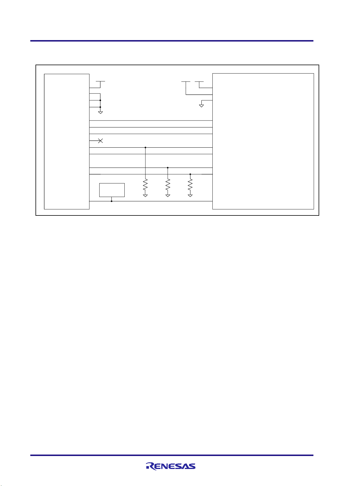
2.4 Examples of recommended connections between the connector and MCU
This section describes examples of recommended connections between the target MCU and interface circuit.
2.4.1 Example of recommended connections
Multiple recommended examples for connection are given in accord with the purposes for which the emulator is to be
used. Select the appropriate circuit with reference to the table shown below. Be sure to take the specifications of the
target device as well as measures to prevent noise into consideration when designing your circuit.
Both debugging (4-pin LPD) and programming (2-wire UART)
Only programming (2-wire UART)
Purpose
Figure
Figure 2-4
Figure 2-5
R20UT3433EJ0300 Rev.3.00 Page 9 of 44
Oct.09.20
Page 10
E1/E20/E2 Emulator 2. Connecting the Emulator and User System
14-pi n connector
8
2
12
14
7
5
1
9
3
11
4
6
13
Target device
SYSVCC
VCC
VSS
LPDI / FPDR(FLSCI3R X)
LPDO / FPDT(FLSCI3TX)
LPDCLK I / FPCK(FLSCI3SCK)
LPDRS T
LPDCLK O
MD0
FLMODE
RES
TVD D
GND
GND
GND
LPDIO / FPDR
LPDO / FPDT
LPDCLK / FP CK
TRS T
LPDCLK OUT
FPM D0
FPM D1
RESET
RESET
circuit
1K to
10K
1K to
10K
VCC SYSVCC
VCC
1K to
10K
(1) Connection which allows Both debugging (4-pin LPD) and programming (2-wire UART)
Figure 2-4 Example of Connection
Refer to section 2.4.2, Connecting the RESET pin, for more information on the reset circuit.
For details on TVDD, refer to section 2.4.3, Connecting the TVDD pin.
Make wiring runs between the 14-pin connector and target device as short as possible (within 50 mm is
recommended). Do not connect the signal lines between the connector and MCU to other signal lines.
Use GND to apply a guard ring for the wiring which runs between the 14-pin connector and target device. Do
not route high-speed signal lines parallel to each other or allow them to cross each other.
Pin names may vary among target devices. Refer to the user’s manual for the target device you are using for the
actual pin names.
Proceed with appropriate processing for pins of target devices which do not require connection to the emulator
in accord with the descriptions in “Handling of Unused Pins” in the user’s manual for the target device.
R20UT3433EJ0300 Rev.3.00 Page 10 of 44
Oct.09.20
Page 11
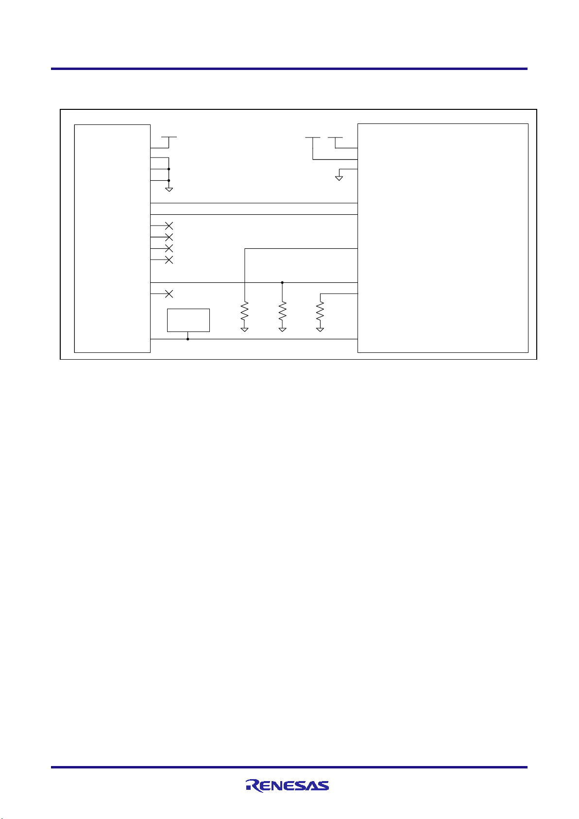
E1/E20/E2 Emulator 2. Connecting the Emulator and User System
8
2
12
14
7
5
1
9
3
11
4
6
13
Target device
SYSVCC
VCC
VSS
FPDR(F LSCI3R X)
FPDT(FLSCI3TX)
LPDRS T
MD0
FLMODE
RES
TVD D
GND
GND
GND
FPDR
FPDT
FPM D0
FPM D1
RESET
RESET
circuit
1K to
10K
1K to
10K
VCC SYSVCC
VCC
1K to
10K
14-pi n connector
(2) Connection which allows Only programming (2-wire UART)
Figure 2-5 Example of Connection
Refer to section 2.4.2, Connecting the RESET pin, for more information on the reset circuit.
For details on TVDD, refer to section 2.4.3, Connecting the TVDD pin.
Make wiring runs between the 14-pin connector and target device as short as possible (within 50 mm is
recommended). Do not connect the signal lines between the connector and MCU to other signal lines.
Use GND to apply a guard ring for the wiring which runs between the 14-pin connector and target device. Do
not route high-speed signal lines parallel to each other or allow them to cross each other.
Pin names may vary among target devices. Refer to the user’s manual for the target device you are using for the
actual pin names.
Proceed with appropriate processing for pins of target devices which do not require connection to the emulator
in accord with the descriptions in “Handling of Unused Pins” in the user’s manual for the target device.
R20UT3433EJ0300 Rev.3.00 Page 11 of 44
Oct.09.20
Page 12
E1/E20/E2 Emulator 2. Connecting the Emulator and User System
RES
RESET
13
Example
SYSVCC
14-pin connector
Target device
2.4.2 Connecting the RESET pin
While you are using the E1, E20 or E2 emulator, pin 13 (RESET pin) of the 14-pin connector must be connected to the
reset pin of the target device. An example is shown in the figure below.
The E1, E20 or E2 emulator fixes the RESET pin to the low level before the debugger is activated. After the debugger is
activated, the emulator either keeps the pin at the low level or places it in the high-impedance state in accord with the
operation of the debugger.
Figure 2-6 Example of Connecting a Reset Circuit
Output of the reset circuit should be either n-channel open drain or be a signal generated solely by a resistor and
capacitor (and possible other components).
For the target device in this user’s manual, pull the RESET signal (RES) up to the SYSVCC voltage.
Pin 13 (RESET) of the E1, E20 or E2 emulator is pulled up (by a 100-kΩ resistor) within the emulator (refer to
section 5, Internal Circuits of the Emulator).
The RESET pin of the target device may be pulled up or down within the device. On this point, refer to the
user’s manual for the target device.
The maximum sink current accepted by the RESET pin of the E1, E20 or E2 emulator is 2 mA. Select an
appropriate pull-up resistance which does not surpass this value.
Adjust the time constant of the reset circuit so that the time elapsing before the signal reaches 80% of the high
level from the low level is within 900 µs.
When you use hot plug-in, consider installation of a capacitor between the reset signal and GND in order to
suppress a noise. In this case, however, the specifications of the time described above must be satisfied.
R20UT3433EJ0300 Rev.3.00 Page 12 of 44
Oct.09.20
Page 13
E1/E20/E2 Emulator 2. Connecting the Emulator and User System
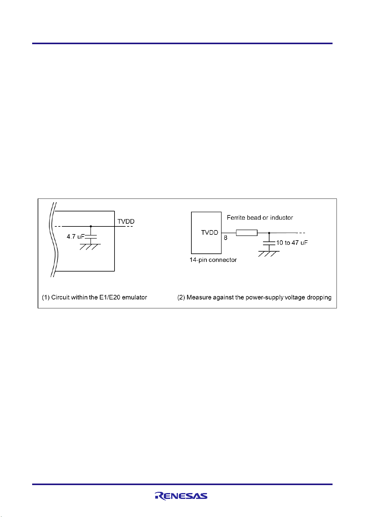
2.4.3 Connecting the TVDD pin
(1) Power source monitoring function
Connect the power source on the user system to pin 8 (TVDD pin) of the 14-pin connector. For the target device in
this user’s manual, this will be the source of the VCC voltage.
The power source connected to the TVDD pin provides power to the final stage output buffer and first stage input
buffer on the E1/E20/E2 emulator circuit. When the E1, E20 or E2 emulator is connected, it will draw current as
described below in addition to the current drawn by the user system.
E1/E2 emulator: Approx. 20 mA when TVDD is 3.3 V, and approx. 40 mA when TVDD is 5.0 V
E20 emulator: Approx. 40 mA when TVDD is 3.3V, and approx. 100 mA when TVDD is 5.0 V
If there is a possibility you will be using hot plug-in connection, you will need to configure the circuit as shown
below. Pin 8 of the E1 emulator is connected to a 4.7-uF capacitor as shown in (1) in Figure 2-7, so hot plug-in
connection of the emulator may lead to a momentary drop in the power-supply voltage on the user system. This
might cause the MCU to be reset. As shown in (2) in Figure 2-7, this effect can be reduced by placing a ferrite bead
(or inductor) and relatively large capacitor with low equivalent series resistance near the TVDD line of the
connector for connection of the emulator. Note that this measure will not completely eliminate the voltage drop.
Note that hot plug-in connection is only for use during debugging, and a separately sold hot plug-in adapter is
necessary to use this function otherwise.
Figure 2-7 Circuit Configuration for Hot Plug-in
(2) Power supply function (applies only to the E1 or E2 emulator)
The E1 or E2 emulator can also supply power at 3.3 V or 5.0 V from the TVDD pin to the user system (at a current
of up to 200 mA). When using this function, take care of the following points.
Do not use this function if power is being separately supplied to the user system. Attempting to do so
might break the E1 or E2 emulator.
Do not use this function for a user system which draws a current of 200 mA or more. The E1 or E2
emulator or USB interface of the host machine might be broken.
Make sure that the supplied voltage is within the voltage range required by the user system.
E1 emulator : The 5.0-V supply depending on the environment of the host machine in use, the voltage
might be lower than 5.0 V by 0.5 V or more.
E2 emulator : The 5.0-V supply depending on the environment of the host machine in use, the voltage
might be lower than 5.0 V by 0.3 V or more.
R20UT3433EJ0300 Rev.3.00 Page 13 of 44
Oct.09.20
Page 14
E1/E20/E2 Emulator 2. Connecting the Emulator and User System
Power supply from the E1 or E2 emulator depends on the quality of the USB power supply of the host machine, and as such,
processes, use the Renesas Flash Programmer.
WARNING
Warning for Turning the Power On/Off:
When supplying power, ensure that there are no shorts between the user system and power circuit. Only connect
fire.
precision is not guaranteed. When writing a program that requires reliability, do not use the power supply function of the E1
or E2 emulator. Use a stable, separate power supply for the user system. When writing a program for mass production
the E1, E20 or E2 after confirming that there are no mismatches of alignment on the user system port connector.
Incorrect connection will result in the host machine, the emulator, and the user system emitting smoke or catching
2.4.4 Hot plug-in adapter for the E1 emulator
For hot plug-in connection to the E1 emulator, use the hot plug-in adapter for the E1 emulator (R0E000010ACB00)
that is separately available from Renesas.
2.4.5 Isolator for the E1 emulator
For a debugging environment where there is a difference in potential between the GND of the user system and that of
the host PC, use the isolator for the E1 emulator (R0E000010ACB20) which is separately available from Renesas.
2.4.6 Small connector conversion adapter for the E1 emulator
A small connector conversion adapter for the E1 emulator (R0E000010CKZ11) is separately available from Renesas
for user system boards which are too small to mount the 14-pin connector that is the standard connector for the E1
emulator. By using the adapter, you can reduce the area taken up by the connector mounted on your system.
However, when you use the small connector conversion adapter for the E1 emulator, be aware that the pin assignments
of the connector differ from those of the standard interface connector for the E1 emulator.
R20UT3433EJ0300 Rev.3.00 Page 14 of 44
Oct.09.20
Page 15

E1/E20/E2 Emulator 3. Specifications
Broad Category
Medium Category
Narrow Category
Specification
Hardware in general
Corresponding host machine
Computer equipped with a USB port,
OS depends on the debugger
User system interface
14-pin connector
Host machine interface
USB 2.0 (full speed or high speed)
interface cable
Power supply function (only when the
3.3 V or 5.0 V (with current up to 200 mA)
system (make settings with the debugger)
through the USB)
Debugging-related
Break
Software break
In ROM and RAM areas combined: 2000
points
conditions)
Event break
Available
Forced break
Available
Trace-full break
Available (internal trace memory and E2
storage)
break
Event
Number of events that
8 points for execution, 8 points for CPU
points for GRAM access
Available function
Break, trace, performance measurement
Combination of events
OR, sequential
Destination for storage
Internal trace memory
Size
Branch only: 2,000 branches
instructions
software trace
Conditions to start and
stop recording of data
Stopping of program execution, event
condition settings
Data-trace conditions
Event conditions
Priority of trace
Real-time trace mode (priority given to
data)
3. Specifications
Table 3-1 shows specifications common to the E1, E20, and E2 emulators.
Table 3-2 shows specifications specific to the E2 emulator.
Support for some debugging-related functions also depends on the debugger. Refer to the user’s manual, etc. for the
debugger you are using.
Table 3-1 Specifications Common to the E1, E20, and E2 Emulators
Connection to the user system Connection by the provided user system
items
emulator is an E1 or E2)
Power supply for the emulator No need (the host computer supplies power
Hardware break 12 points including those used for both
External trigger input
can be set
Tracing
(only for devices
including an
internal trace RAM)
can be supplied from TVDD to the user
execution and CPU access conditions (8
points only for execution conditions, and 4
points for either execution or access
Available (E2 emulator only)
access, 4 points for DMA access, and 4
Data trace only: 2,000 cycles of access
Software trace only: 2,000 to 4,000
R20UT3433EJ0300 Rev.3.00 Page 15 of 44
Oct.09.20
Traced data Branches, cycles of data access, cycles of
DMA access, cycles of GRAM access, and
acquisition
speed)
Non-real-time trace mode (priority given to
Page 16

E1/E20/E2 Emulator 3. Specifications
Broad Category
Medium Category
Narrow Category
Specification
Recording of trace
Ring mode (overwriting mode)
trigger (E2 emulator only)
Perfor-
Time (1)
Measurement section
From run to break
Item measured
Execution time*4
Performance
32-bit counters
Time (2)
Measurement section
From run to break, or between two event
points
Items measured
Execution time, total execution time, pass
execution time*4
Performance
32-bit counters (for three sections)
Other
Items measured
Number of instructions executed (all or
cache
Measurement section
From run to break, or between two event
points
Items measured
Maximum value, minimum value, latest
value, total value, pass count
Performance
32-bit counters (for four sections)
Pseudo real-time RAM monitoring
Available (occupies a bus (steals cycles))*1
Direct memory modification
Available (occupies a bus (steals cycles))*1
Debugging console
Not available
Downloading of the external flash memory
Not possible
Hot plug-in
Possible (To use with the E1 emulator,
adapter)
Peripheral breaks
Available*2
Emulator detection by user programs
Available*3
FE60 2078H (PCU)
Security
16-byte ID code authentication
Security ID settings
Not available
Security flag settings
Not available
Activating the settings of the Intelligent
Cryptographic Unit (Slave type) (ICUS)
Not possible
Connection interface
4-pin LPD 5.5 MHz /11 MHz /16.5 MHz /
33MHz(E2)
Programming-related
Security ID settings
Available
Security flag settings
Available
Activating the settings of the Intelligent
Cryptographic Unit (Slave type) (ICUS)
Possible
Connection interface
2-wire UART
mance
measurement
than
time
memory
Trace-full stop mode
Trace-full break mode
Halting tracing due to the input of an external
count, maximum execution time, minimum
branches only), number of interrupts
accepted (EI level or FE level), number of
exceptions accepted (instruction
asynchronous or instruction synchronous),
clock cycles (all, while interrupts are
inhibited, or other than for the processing of
interrupts), number of instruction fetches
requested, number of hits on the instruction
items
R20UT3433EJ0300 Rev.3.00 Page 16 of 44
Oct.09.20
requires a separately sold hot plug-in
Debugging startup register
Initial value: 0000 0000
Address: FA00 2078
H
(CPU1)
H
Page 17

E1/E20/E2 Emulator 3. Specifications
Note 1: Only available for the general local RAM and global RAM areas.
Note 2: The function to stop peripheral I/O operation in a break is called the peripheral break function.
Whether peripheral emulation functions are set or not is determined by the debugger.
Refer to the manual for the debugger you are using for how to set them.
Refer to the manual for the MCU you are using to check whether peripheral emulation functions are set.
Note 3: For this function, any 32-bit value which is debugging information from the debugger is specified and held in the
debugging startup register while the emulator is connected. This function can be used to determine the state of the
emulator being connected or not from within user programs (refer to cautionary note No.41 of section 4.2).
Note 4: The resolution of the measured times depends on the interface used for the connection (e.g., 90.9-nsec resolution
for a 4-pin LPD connection running at 11 MHz).
R20UT3433EJ0300 Rev.3.00 Page 17 of 44
Oct.09.20
Page 18

E1/E20/E2 Emulator 3. Specifications
Broad Category
Medium Category
Narrow Category
Specification
the synchronous debugging mode).
Destination for
storage
“E2 storage”: memory for storage in the E2
emulator
Internal buffer
Eight stages*4
Traced data
Software trace data + timestamps (given by the
Resolution: 8.333 ns, maximum 27 days
data
Priority of trace
CPU1:
Real-time trace mode (priority given to speed)
Trace-full break mode
External trigger
Input signal channels
E2 expansion interface: 2
ch. 0: pin 11, ch. 1: pin 12
channels
ch. 0: pin 9, ch. 1: pin 10
Interface voltage
When the emulator is not supplying power to
Voltage being supplied to the user system
inputs
Operation when a
When software tracing (LPD output) is in use:
memory
outputs
Operation when a
trigger is output
Output of a low or high pulse (for from 1 µsec to
65535 µsec) can be specified.
Table 3-2 Specifications Specific to the E2 Emulator
Debugging-related
items
Software tracing
(LPD output)*
1
Target CPU Selection of a single CPU.
For multiple-core devices:
When the debugger is connected to the
emulator, a single target CPU is selected. If the
target CPU is changed, the debugger must be
re-connected to the emulator (only available in
E2 emulator)*2
Conditions to start
and stop recording of
acquisition
Recording of trace
memory
Starting and stopping of program execution
(breaks)
Real-time trace mode (priority given to speed)
Non-real-time trace mode (priority given to
data)
PCU:
Ring mode (overwriting mode)
Trace-full stop mode
input/output*1
Output signal
Conditions for
detection of trigger
trigger is input
Condition for
detection of trigger
E2 expansion interface: 2
the user system:
TVDD voltage
Any voltage between 1.8 V to 5.0 V
When the emulator is supplying power to the
user system:
Edge detection (rising, falling, or both edges)
Level detection (low or high)
Break
When software tracing (LPD output) is not in
use:
Break or stopping of recording in internal trace
Break detection*3
Note 1: When the software tracing (LPD output), external trigger input, or external trigger output functions are in use,
access to memory during the execution of a program, changes to event conditions, the reading of internal trace
memory, and the display of state indicators such as STOP are disabled.
R20UT3433EJ0300 Rev.3.00 Page 18 of 44
Oct.09.20
Page 19

E1/E20/E2 Emulator 3. Specifications
Note 2: A timestamp indicates the time that the E2 emulator acquires the software tracing data, not the time the
instruction in the software being debugged was executed. The E2 emulator requires execution of the program by
the MCU to start only after it has started counting its timestamp values. Since the start of counting of timestamp
values cannot be precisely synchronized with the start of program execution, the timestamps which have been
added to the software tracing data stored from the head of the E2 storage may include some errors.
When the software tracing (LPD output) function is not in use, breaks are not detectable during the 10-µsec
Note 3:
period after a program has started to run.
Note 4: The output of the combination of a PC value and the corresponding immediate or register value uses one stage of
the internal buffer. When software tracing data have been stored up to the seventh stage of the internal buffer, an
overflow message is stored in the eighth stage.
R20UT3433EJ0300 Rev.3.00 Page 19 of 44
Oct.09.20
Page 20

E1/E20/E2 Emulator 3. Specifications
4-pin LPD (33 MHz)
DBTAG imm10
Outputs a 10-bit immediate (imm10)
3.1 Overview of specifications specific to the E2 emulator
3.1.1 Software tracing (LPD output)
Devices of the RH850 family support debugging instructions for the output of software trace data. Software trace data are
stored in the internal trace memory of the device and output to the emulator via the LPD pins, which is the debugging-
connection interface. Unlike conventional tracing, the software tracing function does not cater for the setting of events or
conditions so that trace data are output when the settings match the results of program execution; instead, this function
helps the user to embed debugging instructions in the program to be executed as checkpoints or for the purpose of the
output of specific information or register values and output of the history execution to the emulator side as trace data.
Make use of this function as a new way of debugging. The debugger of CS+ provides useful functionality for applying
this software tracing function (via the LPD interface). For details, refer to the user’s manual and application note for
CS+.
For details of the debugging instructions, refer to the RH850 G3M/G3MH/G3K/G3KH User’s Manual: Debugging
Instructions. Table 3-3 gives an overview of these instructions.
When the emulator is not connected and the debugging instructions embedded in a program are executed, Software trace
data are not output from the LPD interface.
Table 3-3 Debugging Instructions for Software Tracing
Debugging Instruction Function Interval between Execution of the
Embedded Instruction and the LPD
Output (*)
DBCP Outputs the current PC value as software
trace data.
value as software trace data.
Output of the PC value is also selectable.
DBPUSH rh-rt
(General-purpose
registers are specified as
rh ≤ rt (in ascending
order).)
Outputs the register numbers and values
of general-purpose registers from rh to rt
as software trace data.
Output of the PC value is also selectable.
1.727 usec
0.576 usec
(without the PC value)
1.727 usec
(Output one register without the PC value)
(*) This item indicates the time required for the LPD output of software trace data generated by executing a debugging
instruction. When this interval follows the execution of a debugging instruction, overflows (losses) of software trace data
can be avoided. Even if the debugging instruction is executed with a short interval, the device has an internal buffer for
tracing and an overflow (a loss of data) will not occur immediately; however, note that an overflow occurs if the internal
buffer becomes full. For DBPUSH instruction,
set the total number of the registers to less than 5 to avoid an overflow.
R20UT3433EJ0300 Rev.3.00 Page 20 of 44
Oct.09.20
Page 21

E1/E20/E2 Emulator 3. Specifications
3.1.2 External trigger input and output
Using the expansion interface of the E2 emulator (the connector for the interface can be found by removing the cover on
which SELF CHECK is printed) enables the input and output of external triggers. For details on the function, refer to
Table 3-2. For details on the expansion interface, refer to the E2 Emulator User’s Manual.
Figure 3-1 Expansion Interface of the E2 Emulator
R20UT3433EJ0300 Rev.3.00 Page 21 of 44
Oct.09.20
Page 22

E1/E20/E2 Emulator 4. Notes on Usage
4. Notes on Usage
Cautionary notes on using the E1, E20 or E2 emulator are given below.
4.1 Notes on differences in operation between the actual device and the E1, E20 or E2 emulator
No.1 DBTRAP instruction
The DBTRAP instruction is used for software break functions and thus cannot be used in programs with the emulator.
No.2 AUDR function
When an emulator is connected, the advanced user debugger RAM monitoring (AUDR) function, which supports
debugging of a program while mounted on a system, cannot be used.
No.3 Serial programming function
The serial programming function cannot be used with the emulator during debugging.
No.4 HALT mode (skipped number)
The information that was previously under this number has been integrated into section 4.2 No.17.
No.5 Power off standby mode
The emulator does not support emulation in the power off standby mode. Confirm operation on power off standby
mode in a state where an emulator is not connected.
No.6 Current drawn
More current is drawn when an emulator is connected than when it is not connected. That is, the target device consumes
more power during debugging than in normal operation since the debugging functions are operating.
R20UT3433EJ0300 Rev.3.00 Page 22 of 44
Oct.09.20
Page 23

E1/E20/E2 Emulator 4. Notes on Usage
No.7 Initialization of RAM areas
When an emulator is connected, local RAM, global RAM, and FCU-RAM areas are initialized to 0000 0000
. This
H
leads to the following differences from the actual device.
- The initial values in the RAM area after starting an emulator are different from the initial values (undefined
values).
- ECC errors due to non-initialization of RAM are not detected with the emulator. If the emulator is not connected
and the operation is incorrect, check that RAM areas have been initialized.
To emulate ECC errors, set the following options.
- The RAM area is not initialized when the emulator is started.
- OPJTAG is not set for an LPD connection before the emulator is connected.
However, if a RAM area is not initialized, the following functions are not available.
- Downloading to on-chip flash memory
- Changes to on-chip flash memory by using the [Memory] panel or the [Disassemble] panel
- Setting of software breaks
No.8 OTP flag
Do not set the one-time programming (OTP) flag in self-programming with the emulator. Note that setting of the flag
makes downloading from the debugger to flash memory impossible.
No.9 Operation in response to resets and interrupts when an emulator is in use (skipped number)
The information that was previously under this number has been integrated into section 4.2 No.15 and No.16.
No.10 Option byte register
The debugger cannot write new values to the bits of the option byte register indicated below since they are used by the
emulator. Also, do not attempt self-programming to write new values to these bits.
• OPJTAG1 and OPJTAG0 bits (bits 30 and 29 of the OPBT2 register)
The value of the OPJTAG1 and OPJTAG0 bits is always "01B" while an emulator is connected.
• STMSEL1 bit (bit 1 of the OPBT0 register)
The value of the STMSEL1 bit is always 0 while an emulator is connected.
R20UT3433EJ0300 Rev.3.00 Page 23 of 44
Oct.09.20
Page 24

E1/E20/E2 Emulator 4. Notes on Usage
4.2 Cautionary notes on debugging
No.1 Handling of devices which were used for debugging
Do not use devices that were used for debugging in mass-production. This is because writing to the flash memory of
such devices has already proceeded during debugging, so we cannot guarantee the number of times rewriting of the
flash memory can proceed. Debugger errors occur when programming of the flash memory is no longer possible.
Replace the device in such situations.
No.2 Power to the target system while debugging
Do not turn the power to the target system off during debugging. Doing so will require reconnection of the debugger.
No.3 Hardware break (access) function (the timing of a break occurring)
When the hardware break (access) function is in use for CPU1, a break in response to the reading or writing of
specified data will occur after the instruction. Other hardware breaks (access) occur before the instruction.
When the hardware break (access) function is in use for the PCU, a break in response to the reading or writing of
specified data by a read–modify–write instruction will occur after the instruction. Other hardware breaks (access) occur
before the instruction.
No.4 Hardware break (access) function (64-bit data comparison)
When the hardware break (access) function is in use and a data comparison break is set for 64 bits of data, the break
will occur even if the data do not match. A 64-bit hardware break (access) function must not be used with data
comparison enabled.
No.5 Hardware break (access) function (SYSCALL instruction)
For the PCU, hardware breaks are not generated by a read access of the SYSCALL instruction.
No.6 Hardware break (access) function (EIINT table)
Do not set the address of the EIINT table as a hardware break condition. If a break occurs, it will not be possible, in
some cases, to return from the interrupt processing even if EIRET is executed.
R20UT3433EJ0300 Rev.3.00 Page 24 of 44
Oct.09.20
Page 25

E1/E20/E2 Emulator 4. Notes on Usage
No.7 Debugging interface
The E1, E20 and E2 emulators support only 4-pin LPD interface.
Operation is as follows if the setting of the OPJTAG1 and OPJTAG0 bits of the option byte 2 register is "11B" (JTAG:
the JTAG interface is selected in the case of a blank chip).
a. When starting (connecting) the E1, E20 or E2 emulator
Settings of the option byte 2 register are changed from the setting for JTAG to that for 4-pin LPD by
the debugger on connection to an emulator.
Therefore, the OPJTAG1 and OPJTAG0 bits of the option byte 2 register are "01B" (4-pin LPD) during
emulator operation.
b. When exiting from a session with (disconnecting) the E1, E20 or E2 emulator
Settings of the option byte 2 register can be changed by the debugger.
- The value of the OPJTAG1 and OPJTAG0 bits of the option byte 2 register can be changed to "11B"
(for JTAG), which requires rewriting of the flash memory.
- The setting of the OPJTAG1 and OPJTAG0 bits of the option byte 2 register can be left as "01B" (4-
pin LPD).
When 4-pin LPD interface is also used the next time the emulator is connected, we recommend exit
from the program without changing the settings from that for the LPD interface.
If power to the target system is turned off because of an abnormal end to the emulator session, OPJTAG1 and
OPJTAG0 bits of the option byte 2 register are not rewritten and so retain the value "01B" (for 4-pin LPD). If you wish
to change the OPJTAG1 and OPJTAG0 bits of the option byte 2 register to "11B" (for JTAG), please do so at the end
of the E1, E20 or E2 emulator session.
No.8 Initialization of RAM areas
All RAM areas for use by a program must be initialized when an emulator is in use. Before the emulator is used, if any
setting is made to initialize the RAM area when the emulator is started, ECC errors are not generated since the
debugger initializes the RAM area. However, when the actual device is operated with a program which does not
initialize the RAM area, ECC errors will be generated, preventing normal program operation.
ROMization is also required because any data downloaded from the emulator to the RAM area before program
execution will also be initialized. For details, refer to the user’s manual for the compiler you are using.
No.9 Reset of pins (skipped number)
The information that was previously under this number has been integrated into section
4.2 No.15.
R20UT3433EJ0300 Rev.3.00 Page 25 of 44
Oct.09.20
Page 26

E1/E20/E2 Emulator 4. Notes on Usage
No.10 Trace function (when a device with a trace function is in use)
The following restrictions apply to the trace function.
- In the case of section trace, for example, the instruction immediately before the fetched instruction that actually
caused tracing to start might be included in trace data.
- In some cases, acquired trace information will be lost. This depends on the program being executed. The lost
information cannot be restored, but the fact of the loss is indicated (displayed). Information is lost when access to
data by the CPU is continuous and frequent.
- When priority in tracing is given to non-realtime operation, the functions to stop tracing when the trace memory
becomes full (trace-full stop function) and when a specified number of trace messages have been acquired
following an event (trace delay-stop function) are not available. To use these functions, give priority to realtime
operation.
- When data-qualified tracing (point tracing), i.e. tracing only of data in access to a specific address, is specified,
tracing proceeds with any data conditions ignored, even if read or write access conditions are set. Tracing is still
governed by conditions other than data conditions.
- If the program to be traced includes an LD.DW or ST.DW instruction (i.e. an instruction for access to 64 bits of
data), the results for tracing of data access may not be correctly displayed. Only use branch tracing with such
programs or use data-access tracing with programs which do not include LD.DW and ST.DW instructions.
No.11 Quality of flash programming
To improve the quality, follow the guidelines below.
• Circuits are designed as described in the user's manuals for the MCU and E1, E20 or E2 emulator.
• The MCU, E1, E20 or E2 emulator, and the software are used as described in respective user's manuals.
• The supply of power to the user system is stable.
No.12 Turing the power on/off
Turn the power of the E1, E20 or E2 emulator and the user system following the procedure below.
When a separate power supply is used for the user system
<When using the emulator>
(1) Check the power is off.
Check that the user system is turned off. When using the E20 emulator, check its power switch is off.
(2) Connect the user system.
Connect the emulator and the user system with a user-system interface cable.
(3) Connect the host machine and turn on the emulator.
Connect the emulator and the host machine with a USB interface cable. The E1 or E2 emulator is turned on
by connecting the USB interface cable. When using the E20 emulator, turn on its power switch.
(4) Turn on the user system.
Turn on the user system.
(5) Launch the debugger.
Launch the debugger.
R20UT3433EJ0300 Rev.3.00 Page 26 of 44
Oct.09.20
Page 27

E1/E20/E2 Emulator 4. Notes on Usage
CAUTION
Notes on the User System Power Supply:
The user system may be damaged due to leakage current.
<When finished using the emulator>
(1) Close the debugger.
Close the debugger.
(2) Turn off the user system.
Turn off the user system.
(3) Turn off the emulator and disconnect the emulator.
When using the E20 emulator, turn off its power switch. Disconnect the USB interface cable from the E1,
E20 or E2 emulator. The E1 or E2 emulator is turned off by disconnecting from the USB interface cable.
(4) Disconnecting the user system.
Disconnect the user-system interface cable from the user system.
While the power of the user system is on, do not turn off the host machine, unplug the USB interface cable, or
turn off the power switch of the E20 emulator.
When power is supplied to the user system from the emulator (E1 or E2 emulator)
<When using the emulator>
(1) Check the power is off.
Check that the user system is turned off.
(2) Connect the user system.
Connect the emulator and user system with a user-system interface cable.
(3) Connect the host machine and turn on the emulator.
Connect the emulator and host machine with a USB interface cable, then turn on the emulator.
(4) Launch the debugger.
Launch the debugger and select the setting of power supply to the user system.
<When finished using the emulator>
(1) Close the debugger.
Close the debugger.
(2) Turn off the emulator and disconnect the emulator.
Disconnect the USB interface cable from the emulator, then turn off the emulator.
(3) Disconnecting the user system.
Disconnect the user-system interface cable from the user system.
No.13 STMSEL (option byte 0 register)
When the E1, E20 or E2 emulator is connected, starting the emulator causes the value of the STMSEL1 bit to change
from 1 to 0 since the initial value in the option byte 0 register in the device as shipped is for the serial programming
mode (STMSEL1 = 1).
The user mat is in use when the device immediately after shipment is started for the first time. Thus, if you wish to use
the user boot mat, use the function for rewriting the value of option bytes on the flash option settings tabbed page to
change the mat to the user boot mat by changing the value of the STMSEL0 bit of the option byte 0 register.
R20UT3433EJ0300 Rev.3.00 Page 27 of 44
Oct.09.20
Page 28

E1/E20/E2 Emulator 4. Notes on Usage
State of the device
During a
Single
Executing the
Stepping at C-source
Reset mask
Not masked
Masked*
Not masked
Depends on the debugger
Masked
Masked*
No.14 GRG and PBG
When you are using an emulator, leave both the DEB bit of the MGDGRPROTn register in GRG and PROTDEB bit of
the FSGDxxDPROTn register in PBG with the setting 1 (which allows access by a debug master). Changing either bit
to a value other than its initial value may lead to normal access to memory becoming impossible.
No.15 Resets when an emulator is in use
Table 4-1 shows the states of the device when an emulator is in use and the operation in response to a reset (i.e. a user-
system reset) issued by the user system or the user program. During single-stepped execution, the emulator masks the
user-system reset so that it can continue to emulate the source code of the program line-by-line rather than in realtime.
For C-source-level stepped execution, the reset is masked in different ways depending on the debugger; single-stepped
execution is used or the user program is executed by setting temporary breakpoints. Accordingly, this user’s manual
cannot define whether a reset is masked by the emulator or not, so refer to the user’s manual for the debugger you are
using.
Table 4-1 State of the Device and Masking of User-system Resets by the Emulator
break
specification of
the debugger
stepping
user program
level
- When a reset is issued by the debugger (by using a reset button of the debugger, etc.), the CPU is always reset
regardless of whether the masking of resets is currently enabled or disabled. After a reset from the debugger,
breaks are generated in all CPUs.
- Resets generated in the states marked (*) in table 4-1 are held pending. For example, when a setting for software-
reset processing is made during single-stepped execution or a software reset by setting a register is applied by the
debugger during a break, the reset is held pending and performed after the reset mask is removed.
- Do not allow the generation of a reset in the form of a pin reset from the target system other than while a program
is in execution regardless of the presence of masking as described above. A reset generated while the program is
running may cause the debugger to hang.
No.16 Interrupts when an emulator is in use
Table 4-2 shows the states of the device when an emulator is in use and the operation in response to an interrupt.
During single-stepped execution, the emulator masks interrupts so that it can continue to emulate the source code of the
program line-by-line rather than in realtime. For stepped execution of interrupt processing, set a breakpoint at the start
of the interrupt service routine, then generate an interrupt during the execution of a user program so that the break at the
start of the interrupt service routine is applied. For C-source-level stepped execution, interrupts are masked in different
ways depending on the debugger; single-stepped execution is used or the user program is executed by setting temporary
breakpoints. Accordingly, this user’s manual cannot define whether interrupts are masked by the emulator or not, so
R20UT3433EJ0300 Rev.3.00 Page 28 of 44
Oct.09.20
Page 29

E1/E20/E2 Emulator 4. Notes on Usage
State of the device
During a
Single stepping
Executing the user program
Stepping at C-source level
Interrupts masked*
Interrupts not masked (operation is
Depends on the debugger
refer to the user’s manual for the debugger you are using.
Table 4-2 State of the Device and Masking of Interrupts by the Emulator
break
according to the settings of the user system)
- Interrupts (EIINT, FEINT, and FPI) which have been generated in the state marked (*) in Table 4-2 are held
pending and interrupt processing is performed after the interrupt mask is removed.
No.17 HALT mode and stepped execution of the HALT instruction
If a break occurs, the device is released from HALT mode.
When a HALT instruction is encountered during single-stepped execution (execution in units of assembly instruction),
a break is set at the next instruction following the HALT instruction, and the mode does not change to the HALT mode.
When a HALT instruction is encountered during C-source-level stepped execution, whether or not the transition to the
HALT mode proceeds depends on the facilities of the debugger.
No.18 Cautionary note on connecting an emulator (pin reset)
The reset signal continuing to be asserted while communications between the emulator and MCU are being prepared
when the emulator is connected causes the possibility of incorrect communications. Thus, ensure that the reset signal
does not remain asserted when the emulator is connected.
No.19 Cautionary note on connecting an emulator (time required for preparing to communicate)
When an emulator is connected, a program which was written to the MCU is executed from the reset vector before the
emulator and MCU become able to communicate. Take care on this point.
When debugging of a program written to the MCU creates a problem, eliminate the problem by inserting a waiting time
of at least 5 ms* before executing the program following release from the reset state.
Note: Time required for preparing communications depends on the host PC environment of the E1, E20 or E2 emulator
and the operating frequency of the MCU.
R20UT3433EJ0300 Rev.3.00 Page 29 of 44
Oct.09.20
Page 30

E1/E20/E2 Emulator 4. Notes on Usage
No.20 Cautionary note on connecting an emulator (internal reset)
When the stored program generates an internal reset (software reset or reset caused by the watchdog timer overflowing)
immediately after a release from the initial reset state, the internal reset may be generated before communications
between the emulator and MCU have been established after the emulator is connected, causing the possibility of
incorrect communications.
Accordingly, insert a waiting time of at least 5 ms* before applying an internal reset after a release from the initial reset
state when debugging a program which includes an internal reset immediately after a release from the initial reset state.
Note: Time required for preparing communications depends on the host PC environment of the E1, E20 or E2 emulator
and the operating frequency of the MCU.
No.21 Access to I/O resources in the MCU
Access to I/O resources (registers and RAM) in the MCU by the debugger (i.e. access through the memory or I/O
register window) proceeds in the same way as access from a user program.
Examples (for the actual operation of I/O resources, refer to the manual of the MCU you are using)
- Access to DTS-RAM resources
Normal access will not proceed unless a master (i.e. the CPU or PCU) is allocated to use the channel. When access
is attempted while a master has not been allocated, an error will be detected on the ECM side.
- Access to FCU-RAM resources
Normal access will not proceed unless the FCU-RAM enable bit is set.
- Access to the PBG area
Attempted access to the PBG area will not proceed while the guard is enabled. Also, this is within the scope of
error detection.
R20UT3433EJ0300 Rev.3.00 Page 30 of 44
Oct.09.20
Page 31

E1/E20/E2 Emulator 4. Notes on Usage
No.22 Cautionary point regarding hot plug-in connection
When the OPJTAG [1:0] bits of the option byte register are not set for the LPD operation mode at the time of
hot plug-in connection, a connection error occurs. Thus, before proceeding with hot plug-in connection, set
the OPJTAG [1:0] bits for the LPD operation mode.
Allowing hot plug-in connection prevents usage of the optional isolator for the E1 emulator (the isolator is
only for use with the RH850 and RL78 groups).
Allowing hot plug-in connection prevents the supply of power to the user system by the E1 or E2 emulator.
If hot plug-in connection is not to be used, the RAM area will be initialized* when the emulator is started.
Allowing hot plug-in connection prevents this initialization and makes the masking of pins impossible. Thus,
when the emulator is started without initializing the RAM area to be used by a program, ECC errors occur.
Therefore, make sure to initialize the RAM area to be used by a program before setting up the system for hot
plug-in connection.
After completing hot plug-in connection, the user program will be running. At this time, only the emulator
functions listed below are available.
Read or write access to the internal RAM area
Forced break
CPU reset
Apply a forced break if you wish to return to using all functions supported by the emulator. After the forced
break, functions equivalent to those that can be used after normal starting of a program become available.
Note: The RAM area is only initialized if the setting is made to initialize the RAM area when the emulator is started.
No.23 Cases where hot plug-in connection is not possible
Hot plug-in connection cannot be used when the microcontroller is in any of states listed below.
Reset input state
Power shutoff standby mode
No.24 Cautionary note on asynchronous debugging mode (peripheral break function)
In the asynchronous debugging mode, peripheral break functions cannot be used. Even if peripheral break functions are
enabled, peripheral functions are not stopped.
No.25 Cautionary note on asynchronous debugging mode (reset)
In the asynchronous debugging mode, when any of CPUs is in the break state, no resets are acceptable.
No.26 Cautionary note on asynchronous debugging mode (watchdog timer)
In the asynchronous debugging mode, when any of CPUs is in the break state, counters are stopped in WDTA0 and
WDTA1.
R20UT3433EJ0300 Rev.3.00 Page 31 of 44
Oct.09.20
Page 32

E1/E20/E2 Emulator 4. Notes on Usage
No.27 Cautionary note on asynchronous debugging mode (ECC error)
During execution of a user program, there may be a case that the ECC error function does not normally operate for
flash memory.
Example: When any CPU accesses flash memory during execution of a user program causing an ECC error and another
CPU which is in the break state accesses the same resources in the memory window at the same timing, the debugger
temporarily controls the ECC error and no ECC error occurs in any CPU.
No.28 Cautionary note on asynchronous debugging mode (specific sequence)
During execution of a user program, there may be a case that the specific sequence is not satisfied.
Example: When any CPU accesses the specific I/O register during execution of a user program and another CPU which
is in the break state accesses the same peripheral function in the I/O register window at the same timing, the specific
sequence from any CPU is not satisfied and normal accessing is disabled.
No.29 Performance measurement
In the case of measuring a specific section, if the intervals between the start and the end of one measurement, and
between the end of that measurement and the start of the next is short, the measurement is not possible. To obtain
correct measurements, the interval* should be long enough.
*: The required detection interval depends on the operating frequency and the LPD communications frequency of the
MCU.
No.30 Global RAM error log in non-realtime trace mode (when a device with a trace function is in use)
In non-realtime trace mode, if an error (e.g. parity error) occurs during continuous access to the global RAM, the
details of the error may be incorrect.
No.31 Reset (when a device with a trace function is in use)
If a CPU reset occurs during execution of a user program, debugging functions (breaks, events, traces, timers, etc.) and
operation of the microcontrollers may become unstable.
R20UT3433EJ0300 Rev.3.00 Page 32 of 44
Oct.09.20
Page 33

E1/E20/E2 Emulator 4. Notes on Usage
No.32 Rewriting of on-chip flash memory (Working RAM)
When the debugger performs any operation that involves programming of the flash memory* during a break, part of
the internal RAM area is used as a working RAM area. The 4-KB area (for the E2 emulator) or the 9-KB area (for the
E1 or E20 emulator) from the last address of the local RAM area of CPU1 are initially set as the working RAM area. If
a device has no local RAM area, the retention RAM area is used.
The debugger can change the working RAM area. After the debugger has saved the values from the working RAM area
and rewrites the flash memory, it restores the saved values to the working RAM area. To guarantee the values, it is
required to set an area to which there will be no access by the DMAC or any external master to the working RAM area
so that operation may continue even if the device enters the break state.
Note: Rewriting of flash memory proceeds in response to any of the operations below.
• Downloading to on-chip flash memory
• Changes to on-chip flash memory by using the [Memory] panel or the [Disassemble] panel
• Setting or cancellation of software breaks
• Re-execution after a software break is encountered (including stepped execution)
No.33 Rewriting of on-chip flash memory (clock monitor)
The debugger changes the PLL settings when the flash memory is rewritten*. Thus, rewriting the flash memory raises a
possibility of the frequency becoming higher than that currently in use. If the frequency surpasses the upper limit which
was set by the clock monitor (CLMA), this prevents rewriting of the flash memory. If the change in the clock frequency
due to the debugger is a problem, set [Change the clock to flash writing] in the [Property] panel to [No].
[Changing the PLL setting]
PLL0 is set for no frequency division.
Note: Rewriting of flash memory proceeds in response to any of the operations below.
• Downloading to on-chip flash memory
• Changes to on-chip flash memory by using the [Memory] panel or the [Disassemble] panel
• Setting or cancellation of software breaks
• Re-execution after a software break is encountered (including stepped execution)
No.34 Breaks during execution of code for making clock settings
The flash memory cannot be programmed if a break occurs while the MCU is running code written to memory for
making clock settings (setting of the main oscillator or PLL frequency divider and so on).
If you wish either of the following types of operation to proceed when a break has occurred during clock settings, set
[Change the clock to flash writing] in the [Property] panel to [No].
a. Any operation that involves programming of the flash memory (e.g. re-downloading)
b. Setting or deleting software breakpoints
Also, do not set software breakpoints within code for making clock settings.
R20UT3433EJ0300 Rev.3.00 Page 33 of 44
Oct.09.20
Page 34

E1/E20/E2 Emulator 4. Notes on Usage
No.35 Event functions (64-bit access)
Do not set any access events with the condition in 64-bit units. The emulator may detect access in a unit other than 64
bits as satisfying such conditions or other events may not operate normally.
No.36 Event functions (in the order of event detection)
In the following cases, since the orders of instructions and event detection may not operate as set, to measure the time
or performance in sequential events, section tracing, and desired sections may not be possible.
• For CPU1, an event is set for consecutive instructions but the two instructions are executed at the same time.
• An access event detects adjacent read and write instructions, since the timing of event detection differs in write and
read access and the timing may be detected in the order of reading then writing, even though the instructions are
executed in the order of writing then reading.
• Access events may be detected at the same time since bank A and bank B of the global RAM can be accessed
simultaneously and up to two access events are detectable.
No.37 Event functions (bit-manipulation instructions)
When a read or write access condition is set for an event in CPU1, the writing cycle of read-modify-write generated by
a bit-manipulation instruction is not detected as an event. This condition cannot be used as a trigger for a break, trace
acquisition, or performance measurement in the case of such instructions. Such events can only be detected by
modifying them not to include the data condition.
No.38 Event functions (memory-access detection not possible)
In CPU1, no event will be detected for a load or store instruction* which is subsequent to execution of a bit
manipulation instruction (SET1, CLR1, NOT1, or TST1) or a cache manipulation instruction (CACHE, PREF, or
CLL). An event including such a condition may not correctly act a trigger for a break, or for control of trace acquisition
or performance measurement.
Note: This note applies not only to LD and ST instructions but also to other instructions with memory access
(PREPARE, DISPOSE, PUSHSP, POPSP, SWITCH, CALLT, and SYSCALL), and to table reference in response to
EIINT interrupts.
No.39 Satisfaction of two break conditions before a single break
If another read-access event is detected immediately before a transition to the break state due to a forced break or an
event break, a further break occurs immediately after execution of the program is resumed because the break request
was accepted as a read-access event at the time of resumption.
No.40 Software break functions (RAM areas)
The software break function is implemented by replacing instructions. Thus, note that no break will occur if the value
at an address where a software break has been set is rewritten by a user program which is running.
R20UT3433EJ0300 Rev.3.00 Page 34 of 44
Oct.09.20
Page 35

E1/E20/E2 Emulator 4. Notes on Usage
No.41 Emulator detection by user programs
Even if debugging information is specified, note that the value will be initialized to 0000 0000H if a reset is generated.
Debugging information is specified again when a break occurs in all CPUs and when the user program is re-executed
after a reset.
No.42 Cautionary point regarding trace data acquired by software tracing (LPD output) (only for the E2
emulator)
When a break is generated as a forced break, a trace-full break from the E2 storage, or a break due to the input of an
external trigger, information from a debugging instruction that was executed immediately before the break will not be
stored in the E2 storage.
When a debugging instruction is executed during single-stepped execution and a software break or hardware break is
specified and executed by the debugging instruction, software trace data are not output through the LPD interface.
When trace acquisition is stopped due to a break generated by a software break, hardware break, event break, or trace-
full break from internal trace memory, the history of execution from a DBCP instruction executed in the debugging
area is stored as the final trace data in the E2 storage and internal trace memory after the break in execution.
No.43 Breakpoints in the code flash P/E mode or data flash P/E mode
During debugging of a user program which makes the target device enter the code flash P/E mode or data flash P/E
mode, we recommend using hardware breakpoints rather than software breakpoints.
Since flash memory cannot be programmed while the target device is in the code flash P/E mode or data flash P/E
mode, software breakpoints can neither be added to nor deleted from the code flash memory. Accordingly, actually
adding or deleting them on the target device is not possible. Only add or delete software breakpoints in the code flash
memory after the target device is in a mode other than the code flash P/E mode or data flash P/E mode.
If a break is generated at a software breakpoint in the code flash memory while the target device is in the code flash
P/E mode or data flash P/E mode, the break will be generated at the current address (that of the software breakpoint),
so attempting to execute the user program will again lead to a break and the program will not run beyond the current
address. In such cases, apply a reset.
R20UT3433EJ0300 Rev.3.00 Page 35 of 44
Oct.09.20
Page 36
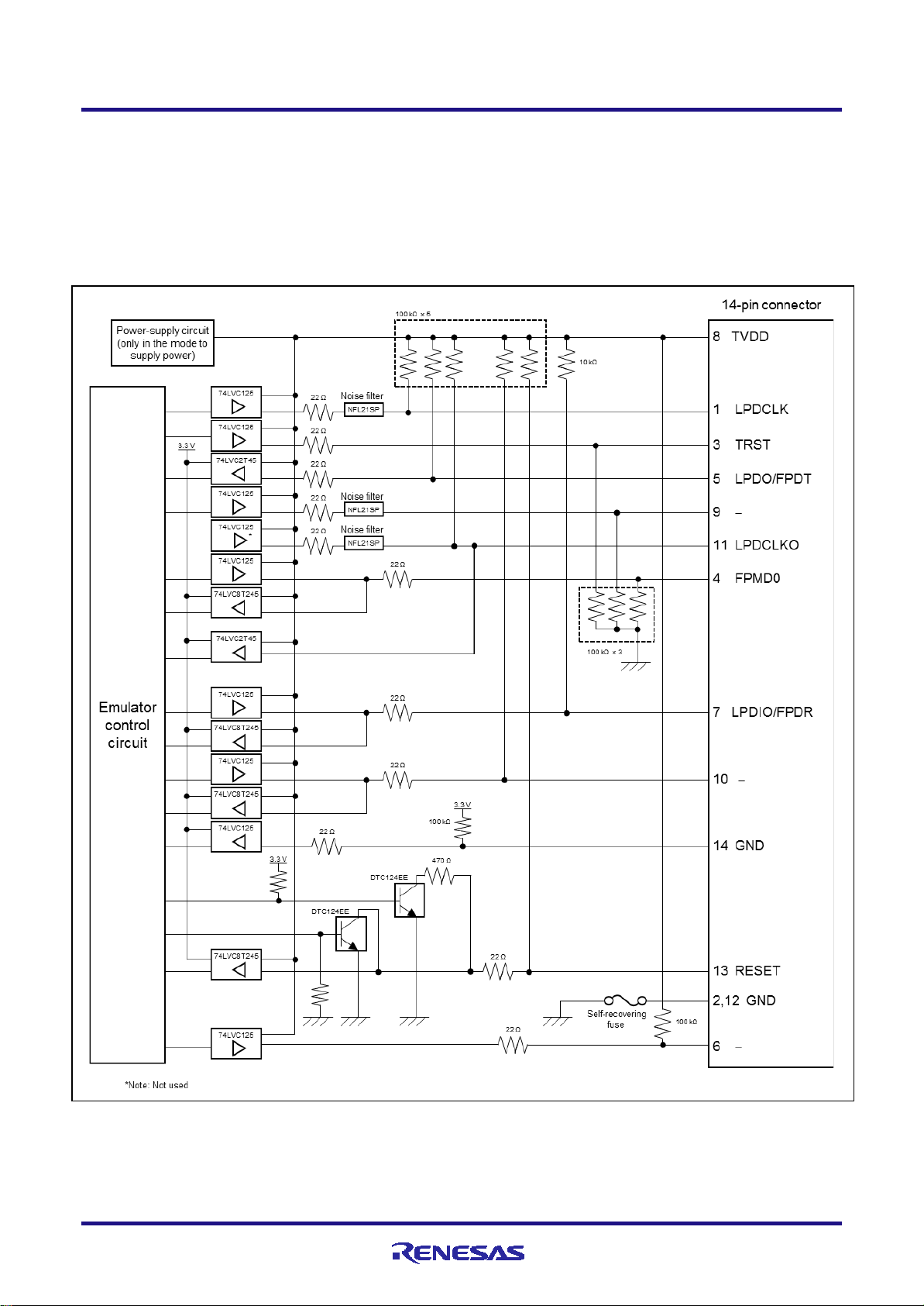
E1/E20/E2 Emulator 5. Internal Circuits of the Emulator
5. Internal Circuits of the Emulator
The internal interface circuits related to the communications interface between the E1 or E20 emulator, the E2 emulator
and user system are shown in figures A and B below. Please refer to the figure when determining parameters in board
design.
Figure A Interface Circuits in the E1 or E20 Emulator (4-Pin LPD, 2-Wire UART)
R20UT3433EJ0300 Rev.3.00 Page 36 of 44
Oct.09.20
Page 37
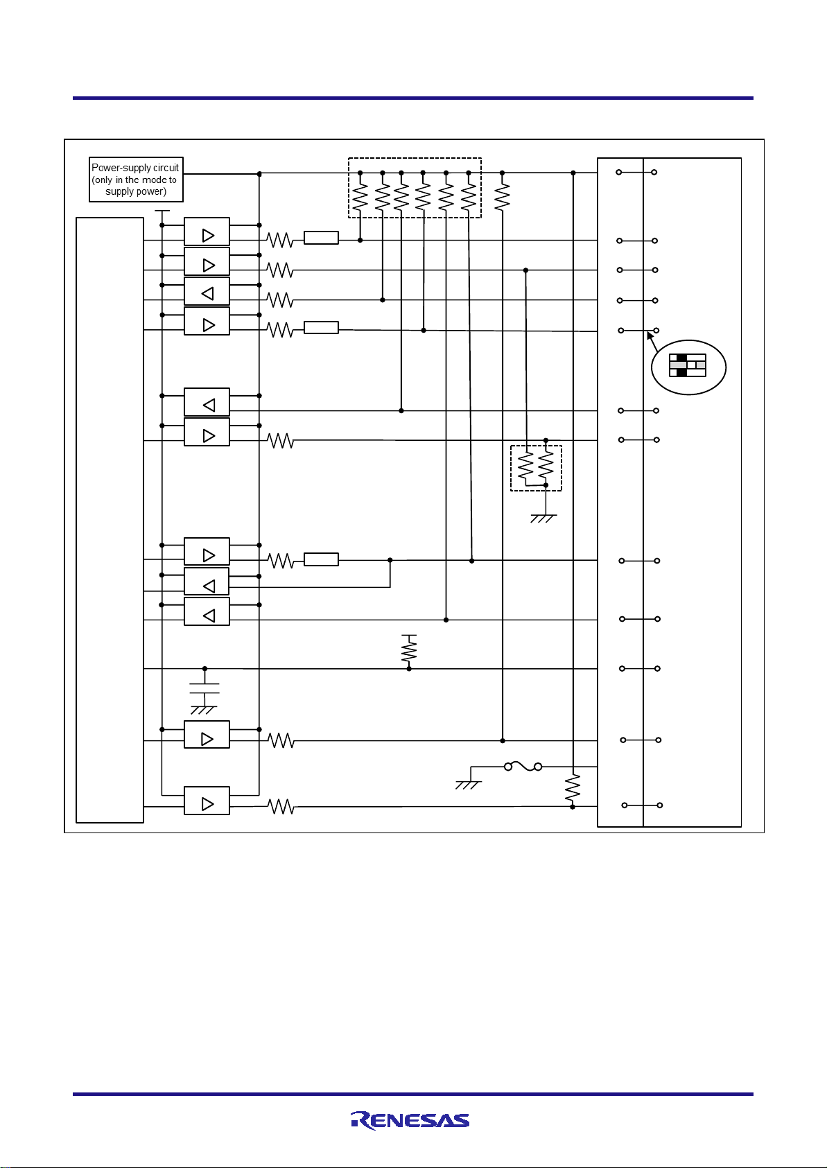
E1/E20/E2 Emulator 5. Internal Circuits of the Emulator
Emulator
control
circuit
74LVC1T45
74LVC1T45
74LVC1T45
74LVC1T45
74LVC8T245
74LVC1T45
74LVC1T45
74LVC8T245
74LVC1T45
NFL21SP
Noise filter
47Ω
1MΩ x6
3.3V
47Ω
47Ω
47Ω
47Ω
NFL21SP
Noise filter
47Ω
3.3V
100kΩ
Self-recovering
fuse
8 TVDD
1 LPDCLK
5 LPDO
3 TRST
9 -
11 LPDCLKO
4 FPMD0
7 LPDI/FPDR
10 -
14 GND
13 RESET
2,12 GND
6 -
74LVC8T245
47Ω
1MΩ
14-pin connector
47Ω
NFL21SP
Noise filter
100kΩ
0.1μF
74LVC1T45
20-pin connector
1
4
16
6
2
12
18
8
20
9
10
14
3,5,15,
17,19
3
1
SW is on 1 side
3MΩ x2
Figure B Interface Circuits in the E2 Emulator (4-Pin LPD, 2-Wire UART)
R20UT3433EJ0300 Rev.3.00 Page 37 of 44
Oct.09.20
Page 38

E1/E20/E2 Emulator 6. Troubleshooting
Problem
Remedy
Error Code in
Inability to connect
When OPJTAG automatic setting is enabled for the setting of the
E1203237
The value set for MainOSC may be wrong. Check whether the
E1203275
• The connection between the emulator and the target device
E1203276
6. Troubleshooting
This chapter gives examples of problems that may arise while the E1, E20 or E2 emulator is being used in combination
with a debugger and of remedies for these problems. Also read the sections of the E1 or E20 emulator user’s manual, E2
emulator user’s manual on the Renesas homepage, and in user’s manuals for debuggers which include FAQs or
information on troubleshooting. The error codes for CS+ are also listed below. If you are using a debugger other than that
of CS+, refer to the user’s manual for the given debugger.
6.1 Problems when the emulator is connected
Table 6-1 Problems when the Emulator is Connected (1/2)
CS+
with the debugging
tool (emulator)
This error may occur
in the serial
programming mode.
debugger, switch the device to the serial programming mode when it
is connected and check and change the value of the OPJTAG bit in
the option byte (see section
shown at right will appear. Check the following items.
• Control of pin resets for the transition to the serial programming
mode may be wrong. When an emulator is connected, do not input a
reset signal to the pin on the circuit other than from the emulator.
Check the notes (e.g. the time the signal takes to reach the high level
from the low level) given in section 2.4.2 or whether the electrical
characteristics requirements of the reset pin of the device are
satisfied.
• The connection between the emulator and the target device may be
wrong. Refer to section 2.4.1, Example of recommended connections,
and check the circuit between the emulator and the target device.
• Check that mode pins such as MD1, which are not controlled by the
emulator, are being handled in ways that allow transitions to the serial
programming mode.
•
frequency of MainOSC on the board matches the value set for
connecting the debugger.
2.3). If this fails, the error message
(particularly that of the FLMD0 pin) may be wrong. Refer to section
2.4.1, Example of recommended connections, and check the circuit
between the emulator and the target device.
R20UT3433EJ0300 Rev.3.00 Page 38 of 44
Oct.09.20
Page 39

E1/E20/E2 Emulator 6. Troubleshooting
Problem
Remedy
Error Code in
Inability to connect
• The OPJTAG bit in the option byte may not be specifying the correct
E1203240
The RESET pin of the target device may be active. Make sure that
E1203274
Inability to connect
• ID authentication may fail when the debugger is connected. Check
C0602202
Table 6-2 Problems when the Emulator is Connected (2/2)
CS+
with the debugging
tool (emulator)
Error in LPD
connection
connection interface (LPD). Enable OPJTAG automatic setting as the
setting for the debugger to allow rewriting of the option byte when the
emulator is started or use a flash programmer (e.g. the RFP) to
change the value of OPJTAG before connecting the debugger.
• The condition in cautionary note No.20 section 4.2 on the time
required for preparing communications before the emulator is
connected to the target device may not be being satisfied. Use a flash
programmer (e.g. the RFP) to erase the code flash memory and
check whether this makes the emulator connectable to the target
device.
• When the emulator is connected other than with a hot plug-in
connection, although the emulator controls the pin reset, this may fail.
Check the notes (e.g. the time the signal takes to reach the high level
from the low level) given in section 2.4.2 or whether the electrical
characteristics requirements of the reset pin of the device are
satisfied.
• The connection between the emulator and the target device may be
wrong. Refer to section 2.4.1, Example of recommended connections,
and check the circuit between the emulator and the target device.
• The specifications for communications may not be being satisfied
due to the state of the target board. Set the LPD transfer rate to a low
rate and check whether the emulator can then be re-connected.
• The value of the option byte may not be correct. Check that the
value of the option byte has been specified with suitable settings
according to the hardware manual for the MCU in use by using a
Flash Programmer (RFP, etc.).
•
the RESET pin is at the inactive level during connection of the
emulator.
with the debugging
tool (emulator)
Non-matching of
security IDs
that the entered ID code is correct.
R20UT3433EJ0300 Rev.3.00 Page 39 of 44
Oct.09.20
Page 40

E1/E20/E2 Emulator 6. Troubleshooting
Problem
Remedy
Error Code in
Inability to generate
• The reset signal may have been at the active level for a long time. If
E1200674
6.2 Problems after the emulator is connected
Table 6-3 Problems after the Emulator is Connected
CS+
breaks
a reset is input for more than 8 seconds, forced breaks will be
disabled. Wait for the end of the reset input or change the setting for
masking resets.
R20UT3433EJ0300 Rev.3.00 Page 40 of 44
Oct.09.20
Page 41

Page
Summary
1.00
Jan. 20, 2017
First Edition issued
15
Table 3-1 was updated.
22-35
Section 4.1 No.4, No.9 and section 4.2 No.9 were skipped.
Correct mistakes in Interface Circuits in the E2 Emulator (74LVC8T45 →
15
Table 3-1 was updated.
“Top cover” was changed to “the connector for the interface can be found by removing
19
Note 4 was added to table 3-2.
38
Remedies for two types of error (E1203275 and E1203276) were added to table 6-1.
Revision History
E1/E20 Emulator, E2 Emulator Additional Document for User's Manual
(Notes on Connection of RH850/E1M-S2)
Revision History
Rev. Date Description
2.00 Jul. 01, 2017 4 Section 1.3 (3) was newly added.
8 Descriptions were added to section 2.3.
18 Table 3-2 was newly added.
20 Section 3.1 was newly added.
Section 4.1 No.8 was modified.
The title of section 4.2 No.3 was changed.
The titles were changed and the descriptions were added in section 4.2 No.15, No.16
and No.17.
Section 4.2 No.42 was newly added.
37
74LVC8T245)
2.10 Jan. 15, 2018 5-6 Descriptions were added in section 2.1.
21
the cover”.
33 Descriptions were added to item No. 32 in section 4.2.
3.00 Oct. 09, 2020 17 Note 4 was added to table 3-1.
31 Descriptions were added to item No. 22 in section 4.2.
35 Section 4.2 No.43 was newly added.
39 A remedy for one type of error (E1203274) was added to table 6-2.
Page 42

Jan. 20, 2017
Jul. 01, 2017
Jan. 15, 2018
Oct. 09, 2020
Rev.1.00
Rev.2.00
Rev.2.10
Rev.3.00
Renesas Electronics Corporation
Colophon
E1/E20 Emulator, E2 Emulator
Additional Document for User's Manual (Notes on Connection of RH850/E1M-S2)
Publication Date:
Published by:
Page 43

SALES OFFICES
Refer to "http://www.renesas.com/" for the latest and detailed information.
Renesas Electronics Corporation
TOYOSU FORESIA, 3-2-24 Toyosu, Koto-ku, Tokyo 135-0061, Japan
Renesas Electronics America Inc. Milpitas Campus
1001 Murphy Ranch Road, Milpitas, CA 95035, U.S.A.
Tel: +1-408-432-8888, Fax: +1-408-434-5351
Renesas Electronics America Inc. San Jose Campus
6024 Silver Creek Valley Road, San Jose, CA 95138, USA
Tel: +1-408-284-8200, Fax: +1-408-284-2775
Renesas Electronics Canada Limited
9251 Yonge Street, Suite 8309 Richmond Hill, Ontario Canada L4C 9T3
Tel: +1-905-237-2004
Renesas Electronics Europe GmbH
Arcadiastrasse 10, 40472 Düsseldorf, Germany
Tel: +49-211-6503-0, Fax: +49-211-6503-1327
Renesas Electronics (China) Co., Ltd.
Room 101-T01, Floor 1, Building 7, Yard No. 7, 8th Street, Shangdi, Haidian District, Beijing 100085, China
Tel: +86-10-8235-1155, Fax: +86-10-8235-7679
Renesas Electronics (Shanghai) Co., Ltd.
Unit 301, Tower A, Central Towers, 555 Langao Road, Putuo District, Shanghai 200333, China
Tel: +86-21-2226-0888, Fax: +86-21-2226-0999
Renesas Electronics Hong Kong Limited
Unit 1601-1611, 16/F., Tower 2, Grand Century Place, 193 Prince Edward Road West, Mongkok, Kowloon, Hong Kong
Tel: +852-2265-6688, Fax: +852 2886-9022
Renesas Electronics Taiwan Co., Ltd.
13F, No. 363, Fu Shing North Road, Taipei 10543, Taiwan
Tel: +886-2-8175-9600, Fax: +886 2-8175-9670
Renesas Electronics Singapore Pte. Ltd.
80 Bendemeer Road, #06-02 Singapore 339949
Tel: +65-6213-0200, Fax: +65-6213-0300
Renesas Electronics Malaysia Sdn.Bhd.
Unit No 3A-1 Level 3A Tower 8 UOA Business Park, No 1 Jalan Pengaturcara U1/51A, Seksyen U1, 40150 Shah Alam, Selangor, Malaysia
Tel: +60-3-5022-1288, Fax: +60-3-5022-1290
Renesas Electronics India Pvt. Ltd.
No.777C, 100 Feet Road, HAL 2nd Stage, Indiranagar, Bangalore 560 038, India
Tel: +91-80-67208700
Renesas Electronics Korea Co., Ltd.
17F, KAMCO Yangjae Tower, 262, Gangnam-daero, Gangnam-gu, Seoul, 06265 Korea
Tel: +82-2-558-3737, Fax: +82-2-558-5338
© 2020 Renesas Electronics Corporation. All rights reserved.
http://www.renesas.com
Colophon 7.0
Page 44

Back Cover
R20UT3433EJ0300
E1/E20 Emulator, E2 Emulator
(Notes on Connection of RH850/E1M-S2)
Additional Document for User’s Manual
 Loading...