

Page 1

·-
•
erv1ce
TRS-BO
Color
Catalog
Computer
Number
26-3026/7
®
2
CUSTOM MANUFACTURED
IN
U.S.A. BY RADIO SHACK, A DIVISION OF TANDY CORPORATION
Page 2

-----------TRS-80
®
-----------
TRS-80®
Color
Computer
2
Service
Manual
Copyright~
1983
Tandy
Corporation
All
Rights
Reserved
Reproduction
or
use,
without
express
written
permission
from
Tandy
Corporation,
of
any
portion
of
this
manual
is
prohibited.
While
reasonable
efforts
have
been
taken
in
the
preparation
of
this
manual
to
assure
its
accuracy,
Tandy
Corporation
assumes
no
liability
resulting
from
any
errors
or
omissions
in
this
manual,
or
from
the
use
of
the
information
contained
herein.
----------ltad1elllaell----------
Page 3

Color
Computer
2
TRS-BO
®
Service
Manual
1/
General
1.1
1.
1.
2/
2.1
2.2
2.3
3/
3.1
3.2
3.3
4/
Introduction
2
System
3
Memory
Specifications
Physical..
Power
Technical.
Disassembly/Assembly
Disassembly
Assembly .....•...........
64K
Theory
Description
Map .
.....
Upgrade
Of
Operation
TABLE
•......
......
.............
.........
Instructions.
OF
CONTENTS
1
.
.
.
1
6
13
13
13
15
16
18
4.1
4.2
4.3
4.4
4.5
4.6
4.7
4.8
4.9
4.10
4.11
4.12
4.13
4.14
4.15
4.16
MC6809E
Reset
Memory
Video
Artifacting
PIAs
ROM •
Keyboard
DAC
SALT
Cassette
RS232
Cartridge
Power
Joysticks
TV
Schematic
Component
Circuit
Circuit
Parts
Circuit
.......
Generation
....•
•••••
Circuitry
Circuitry
Switch
List,
CPU
...
..
.
............
Interface
.....
.•........•.••.
Tape
Connector
Transformer
......
8000191,
Layout
Trace,
Trace,
Format
Connector
Box
.•.
PCB
PCB
PCB
8857636
Circuitry.
..
.
(J3)
(J6).
.........
.
Color
1700235,
8857636,
8857636,
ltadle
.
Information
.
Computer.
Main
Component
Solder
................
..
Logic
Board
Side
Side
..
.
lhaell----------
8857636.
.......
. • ..
19
26
27
31
34
36
39
39
41
44
48
49
51
55
55
56
57
61
.
63
65
67
i
Page 4

Color
Computer
-----------TRS-BO
5/
Troubleshooting
5
.1
Introduction
5.
2
Video
5.2.1
5 . 2 . 2 No
5.2.3
5.2.4
5.2.5
5.2.6
5.2.7
5.
3
Keyboard ...........................................
5.3.1
5.3.2
5.
3.
3
5.
4
Processing
5.4.l
5.4.2
5.5
Cassette
5.5.l
5.5.2
5.5.3
5.6
RS
5.6.1
5.6.2
5.7
5.8
5.9
5.10
Sound
Joystick
Cartridge
Power
Problems
No
Display
Sync
"Garbage"
Clear
No
Color .........................................
Wrong
No
Artifacting
No
Keyboard
Some
Keys
Wrong
General
Symptoms
Motor
Write
Read
2 3 2
Problems
Problems .....................................
Output
Input
Problems .....................................
Supply .......................................
2
®
.
......................................
..
...................................
.......................................
..........•..................•..•.......•..
on
Screen
Screen,
Colors .....................................
No
Or
Entry
Inoperative~
Character
Problems ................................
..........................................
.........................................
Problems ..................................
Control
Problems
Problems
..
..
Missing
Problems ...................................
Problems
Problems .................................
..............................
Signon
Improper
..................•••......
Artifacting
..............................•..
...........................
for
Key
Pressed
.........•....•....•........
.................................
..................................
or
Incorrect
..................................
......................
Service
...........
...............•...
Manual
.
71
.
72
.
72
73
.
73
74
.
74
.
75
75
.
76
.
76
.
76
76
77
.
77
.
77
.
.
80
80
80
.
81
.
81
.
.
81
.
82
.
82
.
82
.
83
.
83
6/
Exploded
Exploded
Parts
Appendices
MC6809E
SN74LS783
MC6847
MC6821
MC6822
----------
Data
Data
Data
Data
View/Parts
View
List
Sheet
Data
Sheet
Sheet
Sheet
List
.......................................
..........................................
Sheet
(Motorola
(Motorola
(Motorola
(Motorola
(Motorola
DS9846-Rl)
ADI-595)
DS9823)
DS9435-R2)
ADI-938)
llad1elhaell----------
98
99
ii
Page 5

Color
Computer
-----------TRS-BO
2
®
-----------
Service
Manual
Fig.
1-1
1-2
1-3
3-1
3-2
3-3
4-1
4-2
4-3
4-4
4-5
4-6
4-7
4-8
4-9
4-10
4-11
4-12
4-13
4-14
4-15
4-16
4-17
LIST
Description
Color
Color
Color
Color
Color
Color
Color
Shield
Power
64K
MC6809E
MC6809E
MC6809E
MC6883
DRAM
DRAM
Color
Color
PIA
Color
DAC
SALT
Color
I/O
RS-232C
Joystick
Antenna
Computer
Computer
Computer
Computer
Computer
Computer
Computer
Clip
Cord
Upgrade.
2
Installation....................
2
Block
2
Memory
Memory
2
2
Memory
2
Memory
2
Memory
Location
Strain
. . . . . . . . . . . . • . . . . . . . . . . . . . . . . . . . . . . . .
Relief
Programming
Pin
Assignments
Read/Write
Reset
Block
Timing......................................
Circuitry
Diagram
Computer
Computer
Block
Diagram................................
Computer
Block
Block
Diagram................................
Diagram
Computer
Circuitry....................................
Connector
Timing
...............................
2
Address
2
Artifacting
2
Keyboard
...............................
2
Power
Pin-Out
Schematic...............................
Switch
Box
Schematic
OF
FIGURES
Diagram...................
Map
Map
Map
Map
(Page
(Page
(Page
(Page
Map C Page
.............................
.........................
Model
........................
..•.......................
at
0.895
...........................
Decoding
Circuitry
Array
Supply
..................
....................
........•....•..........
.....................
1).
. . . . . . . . . . . . 6
2).............
3).............
4)
.............
5).
. . . . . . . . . . . .
MHz
...........
................
...........
Page
No.
2
4
7
8
10
11
16
17
18
20
23
25
26
28
29
31
35
37
40
42
45
46
47
49
55
56
,..
.·
5-1
5-2
5-3
5-4
5-5
5-6
5-7
5-8
5-9
5-10
5-11
5-12
5-13
5-14
Normal
Power
Defective
High
E
VDG
Y
Phase
Phase
Phase
Frequency
and
Q
Clock
and
Phase
Band
Band
Band
Artifacting
Artifacting
Artifacting
Address
Data
Lines
Clocks.
Lines
----------
Supply.
Power
and
Modulator
B...
Phase
Phase
Phase
Supply
Component
. . . . . . . . . . . . . . . . . . . . . . . . . . . . . . . . . .
. . . . . . . . . . . . . . . . . . . . . . . . . . . . . 8 8
...........................
of
Clock
. . . . . . . . . . . . . . . . . . . . . . . . . . . . . . . . .
A
Relationships,
A
Relationships,
A
Relationships,
Signals..............................
Signals..............................
Signals..............................
(Typical)
(Typical)
..........................
.............................
ltadtelhaell----------
iii
+5V
Source
....................
Green
Blue
Red
...........
Screen
Screen
Screen
...
....
..
88
89
90
90
91
92
92
92
93
93
93
94
94
Page 6

Color
Computer
-----------TRS-80
2
®
-----------
Service
Manual
Fig.
5-15
5-16
5-17
5-18
6-1
1
2
3
Description
RAS*
Data
Sound
and
IN
and
Cassette
Color
Line
Computer
Printer
Alternate
Cartridge
CAS*
and
Data
Cassette
Zero
Line
Connector
LIST
...................................
variables
OF
OUT
Output
Crossing
2
Exploded
LIST
Printer
FIGURES
........••••.................
.......................
Detector
View
OF
TABLES
...................•.......
Variable
Signals......................
(con't)
.................
...................
Values
.......•...
Page
.
.
.
No.
95
95
96
96
98
51
52
53
--------------------ladtelhaell-------------------
iv
Page 7

Color
Computer
-----------TRS-BO
1/
General
2
®
Service
Manual
1.1
The
popular
reliable
latest
monitor,
versatility
typical
Interconnecting
control
remember
to
device
The
ROM
program
receptacle
Multipak
be
module
by
peripheral
added
and
Introduction
Color
Color
operation
in
printout
installation
transfer
to
installing
or
Color
which
modules/cartridges
Interface
installed
active
a
switch
to
the
retrieval.
Computer
electronic
the
Computer
is
Computer.
of
the
cables
remove
any
Color
accessed
at
the
at
the
at
on
the
devices,
Color
2
is
as
its
technology.
device,
Color
of
between
all
peripheral
Computer
2
contains
when
right
module
same
any
one
Multipak
such
Computer
a
refined
It
is
predecessor,
or
Computer
the
Color
are
noted
the
power
the
may
side
allows
time
time
Interface
as
an
2
designed
modem
which
major
from
device
2.
an
internal
unit
be
of
the
up
with
selected
external
for
version
Interconnection
provides
2.
Computer
components.
the
to
is
inserted
unit.
to
selection
additional
of
to
provide
but
incorporates
Figure
2.
provide
Color
prevent
BASIC
powered
into
An
four
either
module.
disk
maximum
Computer
program
Radio
to
1-1
shows
signal
Always
damage
program
up.
the
optional
of
the
by
software
Additional
drive,
memory
Shack's
the
same
a
video
a
and
2
prior
to
Other
paks
specific
may
storage
the
the
in
to
or
be
All
must
inputs
exception
the
rear
inputs
connector,
recessed
on
the
1.2
The
by
Random
These
SAM,
RAM,
operate
allow
System
primary
five
five
VDG,
ROM,
communication
be
panel
(right
channel
TV)
40-pin
Access
and
added.
-----------
to
or
of
the
of
and
Power
is
also
Description
functions
Large
Memory
chips
and
two
and
a
provide
outputs
program
the
left),
ON/OFF
switch
located
are
PIAs.
power
a
with
from
module/cartridges,
unit.
Serial
switch,
(for
of
the
Scale
CRAM)
labeled
With
supply,
composite
the
the
Color
These
I/O,
and
selecting
on
the
rear
Color
Integration
and
Read
on
the
only
the
Color
video
outside
Computer
include
Cass
RESET
either
panel
Computer
(LSI)
Only
Block
these
Memory
five
Computer
output.
world,
I/O,
switch.
Diagram
ltadtelhaeli----------
are
the
of
2
chips
I/O
2,
contained
joystick
TV
output
A
channel
the
are
performed
plus
CROM).
as
chips
2
will
However,
interfaces
with
3
unit.
CPU,
plus
or
to
the
on
4
- 1 -
Page 8

Color c ornputer
COLOR
MONITOR
2
TRS-BO
--------~S~e=r~v~i:c:e_~~~~~
®
-
anual
LEFT JOYSTICK
Figure
1-1.
RIGHT JOYSTICK
Color c ornputer
ltad1e lhaell
- 2 -
Installat'
2
----
ion
Page 9

__ c_o_1_o_
The
Processor
provide
this
limited
data
r_ c_o_m_p_u_t_e_r_ 2
main
.
or
data.
set
component
Unit
request
In
of
____
of
any
(CPU,
addition,
mathematical
U23).
data
TRS-BO
computer
It
is
and
select
the
CPU
and
®
system
the
the
is
capable
logical
is
function
proper
operations
Service
the
of
address
of
performing
Central
the
on
Manual
CPU
to
for
a
the
ROM
providing
Without
instructions.
start
and
programmable
residing
RAM
data
eight
1
generate
observed
BASIC
of
A
(Ul2
then
(Ul4
res
instructions).
the
display
programs
central
Synchronous
provides
also
+
ROM,
address
performs
thru
currently
res
(MC6665)
interpreter
provides
the
in
are
the
because
component
refresh
Ul3
in
CPU
the
In
in
devices.
ROM
U21)
being
16K
as
video
will
located
Address
all
Extended
with
CPU
normal
ROM
the
is
x 1 (MCM4517)
an
In
the
use
located
and
of
a
pre-defined
would
operation,
after
reset
Following
in
control
provides
executed.
option
addition,
display.
program
another.
in
RAM.
in
the
Multiplexer
address
the
system
Basic)
run
wild
the
reset
program
of
storage
(see
this
Normally,
will use
Duri
in
ROM
Color
multiplexing
has
set
and
the
switch
to
this,
the
CPU.
for
In
the
but
may
Paragraph
same
ng
will
Computer
(SAM,
timing
the
function
of
randomly
CPU
set
the
the
standard
be
RAM
no
conflict
one
portion
normal
cont
rol
2
U22).
for
and
instructions.
execute
jumps
has
up
BASIC
programs
upgraded
3.3
is
usage,
is
This
device
been
all
interpreter
unit,
for
used
the
the
the
to
of
of
execution
of
the
pressed
the
and/or
these
to
64K x
to
will
chip
RAM.
selection.
be
RAM
the
It
and
The
video
entire
alphanumeric
the
VDG
Adapters
With
composite
circuitry.
this
display
video
is
controlled
(PIAs,
information
video
interface
and
graphic
U2
and
----------1tad1elhae
generator
on
by
and
U7)
and
color
(VDG, U8)
one
chip
modes.
one
of
used
RAM
data
information
- 3 -
The
two
in
,
provides
and
allows
mode
Peripheral
the
the
ll
-
of
Color Computer
VDG
for
the
---------
virtually
several
operation
Interface
generates
modulator
the
of
2.
Page 10

'"Zj
.....
'°
c
t'1
CD
t-'
I
N
.
(')
0
.....
rl
0
t'1
&a.
(')
0
I
9
"O
~
I
c
rt"
(1)
t'1
...
@
N
to
t-'
0
()
;io\"'
0
.....
Pl
'°
t'1
Pl
9
U1
POWER
SUPPLY
I
•5V
-
5V
U23
CPU
MC6809E
CONT
SIGN
AOL
ALS
.
-
us
-
BUF
FER
-
74LS
244
'------
-
,____
IF
-
:
•
~
'
r
CARTRIDGE
CONNECTOR
-
U5
DATA
OUT
-
LATCH
DISPLAY
DATA
74LS
273
~
11
DYNAMIC
RAM
MCM4517
U14
-21
(64K
x
8)
MC6665
~
DEVICE
U22
1---
SELECl
SAM
DYNAMIC
-
U10
RAM
CONTROLLER
74LS02
~
74LS138
MC6883
DATA
ADDRESS
'
t
'
U12
(U13}
SK
OR
16K
x 8
ROM
MC68A364
TV
t
U9
SOUND
MODULATOR
MC1372
I
VIDEO
r------ --------
I
:
SOUND
ua
I
I
VOG
I
GENERATOR
I
MC6847
I
I
U3
I
I
•
..
I r I
I
I 1
I
I I I
I
I
U3
-t
I
U2
~-
~£~~l!f~
--
PIA
r=+
==.i
MC6821
INTERFACE
U1
i-.-
I
l
~
Ul
-
.___
.._
RS
232
INTERFACE
f-4--
"'----
-----------
~
j
l
U7
U3
PIA
--
JOYSTICK
MC6822
INT
ERFACE
T
i
i
KEYBOAR
D
-,
I
I
I
_J
oRcoiii'TiloL:
1
----------
JOYSTICKS
(')
0
t-'
0
t'1
(')
0
9
"O
c
rt"
(1)
t'1
N
~
:D
UJ
I
m
0
@
(/)
(1)
t'1
<:
.....
()
(1)
:s::
Pl
::J
c
Pl
t-'
Page 11

Color
Computer
-----------TRS-BO
The
remaining
to
Input/Output
part
operator
provided
output,
of
this
to
to
and
circuitry
enter
allow
RS-232
2
circuitry
(I/0)
information.
joystick
input
in
the
Color
communication.
is
the
keyboard
Other
inputs,
and
output.
®
Computer
The
which
I/O
cassette
Service
2
most
allows
circuits
input
is
devoted
important
the
are
and
Manual
1.3
The
breakdown
Computer
which
locates
0400
The
for
locations
locations
registers
memory
data
direction
direction
to
clearing
location
as
register
an
Memory
first
may
to
next
the
I/O
allow
an
input
input.
locations.
Map
page
of
2.
be
the
05FF.
two
PIAs.
are
are
determines
register
register
register
configuration
bit
one
sets
of
the
One
located
video
pages
In
the
the
2
and
address
or
an
the
the
Memory
large
variable
anywhere
display
of
the
general,
I/O
registers
control
what
If
this
is
addressed.
is
addressed.
is
addressed
writing
below,
output.
bit
as
blocks
in
at
Memory
registers.
is
of
the
an
Map
of
this
in
the
the
even
addressed
bit
is
data
to
the
each
A 1
in
output
(Figure
memory
block
the
memory.
hexidecimal
Map
explain
numbered
and
the
Bit
set
high
If
it
Normally,
only
even
bit
the
during
inputs
of
data
and
1-3)
in
the
is
the
addresses
the
memory
odd
numbered
two
at
the
(logic
is
set
the
initialization
and
numbered
the
PIA
direction
a 0
sets
shows
Color
video
BASIC
addressing
of
the
even
low,
outputs.
numbered
1),
the
data
memory
may
the
the
display
normally
from
memory
control
the
data
By
be
set
bit
as
----------1tad1elhaell----------
- 5 -
Page 12

Color
Computer
2
-----------TRS-80
®
FF00
C000
A000
4000
2000
1000
0000
HEX
ADDRESS
CARTRIDGE
ROM
t
":;~
t EXPANSION
I
ROM
COLOR COMPUTER
USAGE
16K RAM
Service
Manual
64K
RAM
(ALTERNATE
OPERATING MODE)
0600
ANORMAL
VIDEO
0400 I
DISPLAY
Figure
1-3.
Color
Computer
Memory Map
(page
1)
----------1tad1e/haell----------
- 6 -
Page 13

Color
Computer
2
Service
Manual
-----------TRS-BO
®
-----------
FF00 - FF03
PIA U7
BIT
0 =
KEYBOARD
ROW 1 and
right joystick switch
BIT 1 =KEYBOARD
ROW 2 and
left
joystick switch
BIT 2 =KEYBOARD
ROW
3
FF00
BIT 3 =KEYBOARD
ROW
4
BIT 4 =KEYBOARD
ROW
5
BIT 5 =KEYBOARD
ROW
6
BIT 6 =KEYBOARD
ROW
7
BIT 7 =JOYSTICK
COMPARISON INPUT
Control
of
the Horizontal
0=1RO*to
CPU
Disabled
1=1RQ*
to
CPU
Enabled
sync clock (63.5 microseconds)
0=Flag
set
on
the falling
edge
of
HS
Interrupt Input
BIT 2 =Normally
1:
BIT3=SEL1
:
1=Flag
set
on the rising
edge
of
HS
0=Changes
F F00
to
the data direction register
LSB
of
the
two
analog
MUX
select lines
FF01
BIT
4 = 1 Always
BIT
5 = 1 Always
FF02
FF03
BIT
6 Not
Used
BIT
7 = Horizontal sync interrupt flag
BIT
0=
KEYBOARD
COLUMN 1
BIT
1=
KEYBOARD
COLUMN 2
BIT
2=
KEYBOARD
COLUMN 3
BIT
3=
KEYBOARD
COLUMN 4
BIT
4=
KEYBOARD
COLUMN 5
BIT
5=
KEYBOARD
COLUMN 6
BIT 6=
KEYBOARD
COLUMN
7/RAM
SIZE OUTPUT
BIT
7=
KEYBOARD
COLUMN 8
BIT
0 l .
Control
of
the field sync clock
BIT
1
16.667
Ms
Interrupt Input
l
0=1
RO*
to
CPU
Disabled
1=1RQ*
to
CPU
Enabled
0=
sets
flag on falling
edge
FS
1 =
sets
flag on rising
edge
FS
BIT 2 =
NORMALLY
1:
BIT3=SEL2
:
0=
changes
F F02
to
the data direction register
MSB
of
the
two
analog
MUX
select lines
BIT
4 = 1 Always
BIT
5 = 1 Always
BIT
6
Not
Used
BIT
7 = Field sync interrupt flag
Figure
1-3.
Color
Computer
Memory
Map
(page
2)
-----------
llad1elhaell----------
- 7 -
Page 14
Color
Computer
-----------TRS-BO
2
®
Service
Manual
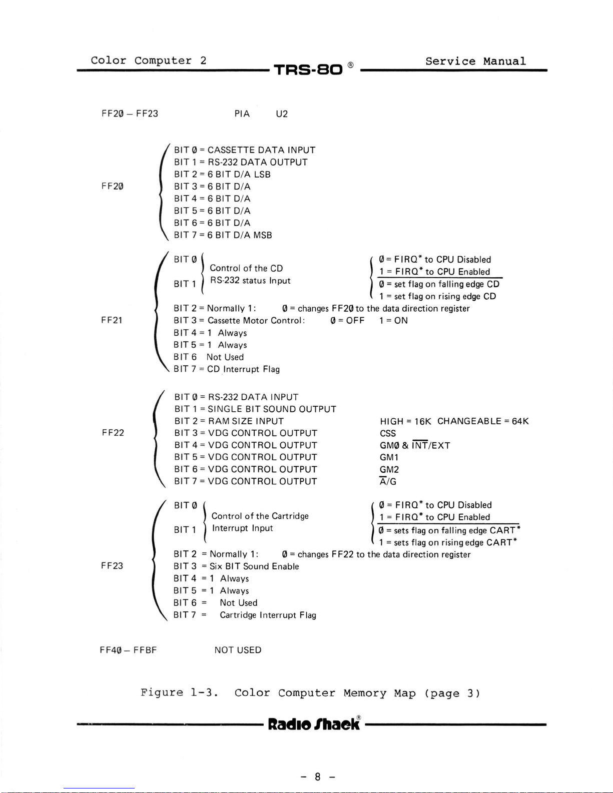
FF20 - FF23
FF20
FF21
FF22
PIA
BIT
0 =CASSETTE
BIT
1 = RS-232
BIT
2 = 6
BIT
BIT3=6BITD
BIT
4 = 6
BIT
BIT
5 = 6
BIT
BIT6=6BITD
BIT
7 = 6
BIT
BIT
0 l
Control
BIT
BIT 2 =Norm
BIT
BIT4
BIT
BIT
BIT 7 =
BIT
BIT
BIT
BIT
BIT
BIT
BIT
BIT
RS-232 status
1
3 =
Cassette
= 1 Always
5 = 1 Always
6 Not
0 = RS-232
1 = SINGLE
2 = RAM SIZE INPUT
3 = VDG CONTROL OUTPUT
4 = VDG CONTROL OUTPUT
5 = VDG CONTROL OUTPUT
6 = VDG CONTROL OUTPUT
7 = VDG CONTROL OUTPUT
CD
Used
Interrupt
DATA
DATA
OUTPUT
D/A
LSB
/A
D/A
DIA
/A
D/A
MSB
of
the
CD
Input
ally 1: 0 =changes
Motor
Control : 0
Flag
DATA
INPUT
BIT
SOUND OUTPUT
U2
INPUT
FF20to
=OFF
0 = FI RO*
1 =
0
=set
l
1 =
the data direction register
1
=ON
HIGH=
to
FIRO*to
flag
on
set
flag on rising
16K
CPU
Disabled
CPU
Enabled
falling
edge
CHANGEABLE=
css
GM0 & I
GM1
GM2
A/G
NT /EXT
edge
CD
CD
64K
BIT
01
BIT
1 Interrupt Input
BIT 2 =Normall
FF23
FF40-
FFBF NOT USED
Figure
BIT
3 = Six
BIT
4 = 1 Always
BIT
5 = 1 Always
BIT
6 =
BIT
7 = Cartridge
1-3.
----------1tad1e
Control
BIT
Not
Color
of
the Cartri
y 1: 0 =chan
Sound Enable
Used
Interrupt
dge
Flag
Computer
- 8 -
0 =
FIRQ*
to
1 =
FIRO*
to
0 =sets flag on falling
l
1 =
sets
flag on rising
ges
FF22
to
the data direction register
Memory Map
(page
lhaell----------
CPU
CPU
Disabled
Enabled
edge
edge
3)
CART*
CART
*
Page 15

Color
Computer
-----------TRS·BO
The
addresses
for
the
SAM
address
data
used
to
and
set
mode.
control
VDG
lines
to
an
even
writing
the
chip
to
control
numbered
register.
To
select
registers
must
any
2
from
the
each
data
all
FFCO
multiplexer
SAM
register.
memory
to
Addresses
a
certain
(V0-V2)
be
set
to
chip;
an
FFDF
therefore,
location
odd
display
and
to
the
®
are
numbered
FFC0-FFC5
the
the
chip
In
general,
will
mode,
PIA
proper
control
(U22).
two
clear
memory
control
the
(U2)
mode.
Service
registers
There
addresses
writing
the
location
the
display
controlling
Manual
are
no
are
any
register
display
mode
the
data
will
Addresses
If
all
at
0000.
display
allows
Register
Color
times.
Addresses
The
Therefore,
Addresses
SAM
Color
only
may
FFDE
cleared,
with
this
of)
available
this
must
Computer
Color
chip.
Computer
by
erase
to
the
bit
the
bit.
not
FFC6
of
the
Normally,
to
the
Pl
FFD6
Computer
FFDA
the
the
FFDF,
the
lower
is
map
for
return
to
registers
start
display
controls
2.
to
registers
to
These
2.
reset
contents
controls
ROMs
32K
set,
and
all
RAM.
The
control
to
FFD3
at
FFD9
FFDD
addresses
routine
occupy
the
control
register
0400.
to
be
a
feature
Therefore,
control
2
is
RO
control
This
of
the
of
address
ROMs
64K
Caution
program
ROM
for
are
cleared,
F2
This
paged
designed
and
Rl
select
memory
in
BASIC.
RAM.
map
the
upper
"disappear"
(less
must
obvious
the
will
feature
through
which
is
should
the
to
should
the
16K
size
Register
type.
space
the
be
must
display
the
be
is
clock
operate
be
memory
or
option
Changes
If
32K
available
from
top
256)
exercised
be
reasons.
display
set
of
all
not
be
speed
cleared.
64K
TY,
this
of
the
in
low
starting
causing
the
SAM
of
the
used
cleared
of
at
0.89
size
setup
of
should
at
at
bit
Memory Map
for
(are
locations
in
memory
address.
will
in
RAM
other
addresses
switched
setting
the
chip
RAM.
the
at
the
MHz.
of
in
be
changed
is
RAM.
are
and
begin
all
CPU.
times
the
the
If
out
The
final
the
interrupt
a
reset
indicated
This
mapped
instance,
contents
dual
or
into
of
series
and
interrupt,
location
set
of
the
if
the
BFFF.
top
----------nad1e111aell----------
of
addresses
reset
it
and
begin
addresses
of
the
CPU
reads
vectors.
will
execution
is
BASIC
FFFF
- 9 -
in
the
load
listed
ROM
it
Color
Whenever
the
address
at
because
(BFF2-BFFF).
will
actually
Computer
the
CPU
at
the
new
the
2
receives
the
location.
vectors
For
read
are
are
the
Page 16

FFDF
FFDE
FFDD
FFDC
FFDB
FFDA
FFD9
FFD8
FFD7
FFD6
FFD5
FFD4
FFD3
FFD2
FFDl
FFD0
FFCF
FFCE
FFCD
FFCC
FFCB
FFCA
FFC9
FFC8
FFC7
FFC6
FFC5
FFC4
FFC3
FFC2
FF
Cl
FFC0
---
Color
Computer
--------T
s
c TYPE
s
c
s
c
s
c
s
c
s
c
TY
M1
M0
Rl
R0
Pl
s F6
c
s
c
s
c OFFSET
s
c
s
c
s
c
s
c
s
c
s
c
s
c
F5
F4
F3
F2
Fl
F0
V2
Vl
V0
2
MAP
MEMORY
SIZE
CPU
RATE
PAGE
#1
DISPLAY
(BINARY)
DISPLAY
MODE
CONTROL
RS-80
(=0)
(=
0)
'I
I
Address
Display Element
N.
U.-
®
-----------
NU
..
-
~32/64K
_
16K
-4K
1
, I
0 0
1
of
1
·0
Upper-Left-Most
- RG6,
0
= 0000 + (%K Offset)
CG6
-RG3
-CG3
I
1 1
1
1
1
1
0
1
0
0
0
1
}
-N.U
1 1
1
-RG2
0
1
1
Service
Dynamic R
.
_N.U.
-0
0 0
1
0
..
-
CG2
I
0
0
1
0
0 1
A
Ms
.9/1
.8 MHz
0.9 MHz
I
0
RGl
C~
,
Al,
0
0
0
Manual
only
AE,
S4
~
Transparent
Refresh
Figure
----
------
1-3.
Color
Computer
ltadte
-
Memory
Map
(page
lhaell----------
10
-
4)
Page 17

Color
Computer
2
-----------TRS-80
®
FFFF
OR
BFFF
RESET VECTOR LSB
FFFE
OR
BFFE
RESET
VECTOR
MSB
FFFD
OR
BFFD
NMI
VECTOR
LSB
FFFC
OR BFFC
NMI
VECTOR
MSB
FFFB OR BFFB SWl1 VECTOR LSB
FFFA
OR
BFFA
SWI
1 VECTOR MSB
FFF9
OR
BFF9
I RO VECTOR LSB
FFF8
OR
BFF8
IRO
VECTOR MSB
FFF7
OR
BFF7
FIRO
VECTOR
LSB
FFF6
OR
BFF6
Fl
RO
VECTOR
MSB
FFF5
OR
BFF5
SWl2
VECTOR
LSB
FFF4
OR
BFF4
SWl2
VECTOR
MSB
FFF3
OR BFF3
SWl3
VECTOR
LSB
FFF2
OR BFF2
SWl3
VECTOR
MSB
FFF1 OR BFF1 RESERVED
FFFO OR BFFO RESERVED
FFEF -
FFEIJ
NOT
USED
Service
Manual
Figure
1-3.
Color
Computer
Memory Map
(page
5)
----------1tad1elhaell----------
-
11
-
Page 18

Color
Computer
-----------TRS·BO
2
®
-----------
Service
Manual
--------------------nad1elhaell---------------
-
12
-
Page 19

Color
Computer
-----------TRS-80
2/
Specifications
2
®
Service
Manual
2.1
2.2
2.3
Physical
Size:
1.
2.
Weight:
Power:
Technical
1.
Microprocessor:
2.
Memory:
Width
Depth
Height
4.75
110
vac
RAM:
ROM:
-
-
lbs
14.
10.35"
3 •
-
(2.15
60
75"
55
Hz,
(37.5
(
26.
II
(9.0
kg)
0.2
Type -Motorola
Clock
16K
Expandable
BK
Standard
BK
Extended
total
Up
to
cartridge)
cm)
cm)
3
cm)
Amps
Speed
of
16K
additional
RMS
-
Basic
Basic
16K
typical
MC6B09E
O.B96
to
64K
(26-3026
(26-3027
Basic
MHz
ROM
ROM
)
) ,
(in
3.
4.
5.
6.
7.
Keyboard:
Video:
Sound:
cassette:
RS232C:
Sources:
53-key
matrix
RF
Modulated
or
4
characters
32
Up
to
Graphic
192
Six-bit
Single
Input
Input
1500
3-wire
Baud
control
microprocessor
output,
by
B
colors
resolution
pixels
DAC
bit
from
from
cassette
cartridge
Frequency
interface
16
rows
up
recorde
Shift
under
scanned
channel
to
256
r
connector
Keying
software
3
x
-----------
llad1e/haell----------
-
13
-
Page 20

Color
Computer
2
Service
Manual
-----------TRS-80
®
-----------
2.3
Technical
Ccon't)
8.
Joystick:
9.
Expansion:
2
connectors,
2
axes
each,
DC
voltage
input
of
0.25
to
4.75
volts
in
64
steps
40-pin
cartridge
connector
con-
taining
all
major
CPU
signals
necessary
for
interface.
----------
lladtelhaell----------
-
14
-
Page 21

Color
Computer
-----------TRS-BO
3/
Disassembly/Assembly
2
®
Service
Manual
3.1
Disassembly
using
pliers.
housing
disassemble
1.
2.
3.
4.
5.
Disassembly
only
are
Disconnect
unit.
Remove
Turn
to
prevent
Loosen
the
come
Turn
cover
care
keyboard
of
the
a
Phillips
Mounting
accessible
the
cartridge
the
unit
and
base
out
the
from
to
to
until
unit
prevent
assembly
Color
screwdriver
screws
computer,
power
damage
remove
the
the
and
from
over
top
the
rightside
bottom
damage
Computer
for
from
follow
remove
slot
and
to
the
the
six
cover.
unit
cover
and
printed
attaching
the
underside
the
signal
(if
place
keyboard
mounting
These
is
turned
up.
and
to
the
2
is
easily
and
a
pair
the
steps
cables
applicable).
it
on a soft
or
screws
screws
over.
Carefully
set
flat
circuit
cable
two
of
noted
top
it
board.
accomplished
of
long-nose
halves
the
unit.
below.
from
surface
cover.
which
may
lift
aside.
not
the
between
of
the
To
the
attach
easily
top
Exercise
the
6.
7.
8.
9.
Disconnect
the
keyboard.
Tag
the
the
left
printed
of
long-nose
Remove
case
from
attach
Remove
two
assembly
rating
three
cover.
the
it
the
attaching
fuse.
from
three
rear
circuit
PCB,
to
transformer
should
the
wires
of
the
board.
pliers.
screws
If
it
do
so
the
PCB.
screws.
be
PCB
the
cable
from
which
is
by
accomplished
the
unit
which
Remove
attach
necessary
removing
from
Replacement
the
which
transformer
are
attached
the
wires
the
to
remove
the
eight
unit
of
using
is
PCB
by
removing
the
the
assembly
using
to
-----------1tad1elhaeli-----------
attached
to
the
the
shield
clips
pigtail
same
at
the
a
pair
bottom
which
the
fuse
type
to
and
-
15
-
Page 22

Color
Computer
-----------TRS-BO
2
®
-----------
Service
Manual
3.2
Assembly
Assemble
disassembly.
metal
There
the
proper
clips.
are
keyboard.
RFI
the
Color
three
shielding.
The
Five
clips
These
Computer
PCB
shield
clips
which
shields
See
2
is
ground
provide
must
Figure
RFI
in
the
reverse
attached
the
shield
RFI
be
in
3-1
SHIELD CLIPS
for
to
to
shield
place
clip
order
the
the
to
of
PCB
with
PCB.
ground
provide
location.
for
RFI
SHIELD
CLIP
When
ensure
plastic
will
reattaching
that
shield
prevent
reconnecting
of
screws
case
parts.
are
Figure
the
between
any
the
used
Ensure
the
wires
damage
top
to
3-1.
wires
are
and
mount
that
Shield
installed
the
to
bottom
the
Clip
from
the
transformer
the
wires
covers.
the
PCB
correct
Location
transformer
in
the
slots
and
the
or
insulation
Two
and
the
type
is
to
PCB.
different
top
and
used
the
of
when
when
PCB,
the
This
types
bottom
reassembling.
The
strain
around
that
relief
the
the
power
to
relief
plastic
the
on
the
bosses
cord
is
transformer
power
at
properly
connections
the
cord
rear
routed
consists
of
the
to
(see
of
unit.
afford
Figure
a
wrap
strain
3-2).
Ensure
-------------------nad1elhaell------------
-
16
-
Page 23

Color
Computer
-----------TRS·BO
MOUNTING
SCREWS
(2) FUSE
2
®
-----------
Service
Manual
Figure
E2
/
3-2.
a_----
Power
TRANSFORMER
PLASTIC SHIELD
ON BASE
Cord
Strain
Relief
TOP
VIEW
----------lladlOlllaell----------
-
17
-
Page 24

__
c_o_1_o_r_c_o_m_p_u_t_e_r_2
____
TRS-BO
®
Service
Manual
3.3
To
following
1.
2.
3.
4.
64K
upgrade
Disassemble
access
eight
Install
8040665
in
noted
Solder
schematic,
Run
operation
in
Upgrade
a
procedure
to
ICs
Ul4
through
with
a
app~opriate
the
reverse
16K
the
from
the
--
total
notch
jumper
LH
of
Instructions
Memory
must
the
RAM
the
64K x 1
U21.
side,
the
order
Unit
be
unit
wire
diagnostic
res,
PCB.
of
in
new
as
ICs
8
ICs)
Ensure
the
at
above
memory
of
to
a 64K Memory
followed:
noted
Ul4
CMC6665,
proper
terminal
disassembly.
in
through
in
place
that
U2).
program
chips.
Paragraph
U21.
Radio
of
chips
location.
Wl
(see
to
Assemble
Unit,
Remove
Shack
the
are
Sheet
verify
the
3.1
to
these
Part
ones
installed
removed
2
proper
the
allow
No.
as
of
unit
00
C3 2 !
C4
(.) (.)
Qo
U14
~
cso -c::>-
U15
~
-c:J-
C51
C52
-c::>-
Figure
~I
U9
-g-~
U20
U17
U18
c:::Jcsg
16
U19
~ ~ ~ ~
C53
-c:J-
Replace
3-3.
these
64K
chips
Upgrade
I
..
Cl
....
..
a:
U21
~~~
-t::>-
C57
-----------
llad1elhaell----------
-
18
-
Page 25

Color
Computer
2
Service
Manual
-----------TRS-BO
®
-----------
4/
Theory
Of
Operation
4.1
MC6809E
CPU
(U23)
The
heart
of
any
computer
system
is
the
Central
Processing
Unit,
or
CPU.
In
the
Color
Computer
2,
as
well
as
most
modern
microcomputers,
the
CPU
is
a
single
Large
Scale
Integrated
Circuit
(LSI).
The
CPU
gathers
instructions
and
data
from
memory,
interprets
and
executes
the
instructions,
and
stores
the
results
of
the
data
operations
into
memory.
Additionally,
the
CPU
stores
data
to
and
retrieves
data
from
various
input/output
CI/0)
devices.
The
Motorola
MC6809E
Microprocessor
is
perhaps
the
most
powerful
8-bit
microprocessor
available
today.
There
are
several
ways
to
determine
the
"size"
of
a
microprocessor
<whether
it
is
8-bit,
16-bit,
32-bit,
or
whatever).
One
way
involves
the
number
of
data
interconnecting
lines
the
processor
possesses.
Another
is
the
size
of
the
internal
registers
and
the
size
of
the
mathematical
and
logical
operations
supported
by
the
processor.
Although
the
MC6809E
has
an
8-bit
data
bus,
internally
it
contains
four
16-bit
registers
and
two
additional
8-bit
registers
which
may
be
linked
together
to
form
another
16-bit
register.
The
MC6809E
also
supports
some
16-bit
mathematical
and
logical
operations.
Therefore,
although
it
is
technically
an
8-bit
processor,
it
has
some
of
the
power
of
the
16-bit
machines.
Figure
4-1
is
a
"programmer's
model"
of
the
MC6809E CPU.
Following
is
a
brief
description
of
the
registers
and
their
respective
functions.
Additional
information
may
be
obtained
from
the
MC6809E
data
sheet.
The
Program
Counter
CPC)
register
is
a
16-bit
register.
It
is
the
job
of
the
program
counter
to
keep
track
of
which
instruction
is
next.
Instructions
for
the
MC6809E
processor
are
from
one
to
five
bytes
in
length.
As
each
instruction
is
fetched,
its
specific
bit
pattern
allows
internal
logic
in
the
CPU
to
determine
the
length
for
that
instruction.
'!'he
PC
is
then
immediately
updated,
even
before
the
remainder
of
a
multi-byte
instruction
is
executed.
The
Hardware
Stack
Pointer
(S)
is
another
16-bit
register.
Its
job
is
to
"point"
to
a
specific
area
of
memory
that
is
set
aside
by
the
systems
programmer
for
the
specific
use
of
the
CPU.
From
time
to
time,
the
CPU
finds
it
necessary
to
"remember"
more
than
it
has
internal
capacity
to
store.
In
these
cases,
it
"pushes
the
data
onto
the
stack".
Later,
when
----------llad1elhaell----------
-
19
-
Page 26

Color
Computer
-----------TRS·BO
2
®
-----------
Service
Manual
15
___
A____,l_I
0
PC
s
- PROGRAM COUNTER
- HARDWARE STACK POINTER
u - USER STACK POINTER
x
y
B-------'
- INDEX REGISTER
- INDEX REGISTER
- ACCUMULATORS
-----------
D
DP
CC - CONDITION CODE REGISTER
Figure
- DIRECT PAGE REGISTER
4-1.
MC6809E
Programming
llad1elllaell----------
Model
-
20
-
Page 27

__
c_o_1_o_r_c_o_m_p_u_t_e_r_2
it
is
ready
from
execution
has
next
instruction
after
to
storing
altering
program
(RTS)
the
already
instruction.
the
return
instruction.
to
stack".
of
updated
will
execution
to
the
return
of
the
flow
____
retrieve
One
a
subroutine.
alter
the
next
PC,
upon
encountering
example
itself
The
Branch
the
of
the
instruction
address
the
TRS-BO
the
information,
of
Recall
to
contain
to
contents
subroutine,
on
the
CPU
is
®
the
that
Subroutine
of
following
stack
able
the
to
Return
use
the
it
of
the
address
the
the
prior
return
from
Service
"pulls
the
program
(BSR)
PC.
CPU
is
the
to
to
Subroutine
Manual
the
data
stack
However,
BSR. By
the
the
is
counter
of
the
required
main
the
The
temporary
Pointer
as
programmer,
hardware-related
Two
registers.
points
much
beginning
book.
table
The
B.
CPU,
mathematical
MC6809E,
double
S
register
instructions.
called
the
S
additional
in
the
Data
by
MC6809E
The
accumulators
and
(D)
storage
as
memory,
same
of
reference
are
the
accumulator,
is
also
of
In
addition,
the
far
as
but
is
storage
16-bit
These
way a book
the
can
CPU
the
and
two
registers
such
Logarithmic
then
(U23)
registers
logical
accumulators
data
U
register.
the
not
registers
be
to
the
contains
are
available
via
the
there
pushing
used
as
which
by
requirements.
can
the
beginning
mark
retrieved
the
operations
can
Tables
pointer
main
upon
can
is
to
Push
is
This
and
the
are
be
mark
from
used.
two
workhorse
which
be
then
the
and
a
dedicated
register
pulling
CPU
for
the
used
the
in
the
(or
8-bit
most
are
combined
a
programmer
Pull
acts
of
data
any
of
X
and
Y
index
to
mark
of
a
page
back
stored
accumulators,
of
performed.
16-bit
specific
data
that
of
registers
the
to
register.
for
user
the
by
its
table,
a
into)
form
Stack
the
is
math
of
In
one
same
the
the
A
and
a
the
----------llad1elhaell----------
-
21
-
Page 28

Color
Computer
-----------TRS-80
2
®
Service
Manual
Another
When
significant
DP
register.
The
individual
individual
processor
programmer
conditions.
8-bit
memory
Condition
C -
V -
Z -
register
is
accessed
eight
Code
bits,
bits
operations.
to
the
an
register
the
set
of
notation.
the
an
rather
are
mask
The
bits
carry
operation
overflow
when
the
register
zero
operation
bits
Register
set
out
are:
bit.
to
store
the
bit.
is
the
in
of
the
than
or
The
two
This
is
greater
bit.
result
to
This
is
equal
Direct
the
Direct
address
CCC)
an
cleared
other
of
the
bit
it.
Similar
is
store
bit
is
8-bit
as
two
three
is
than
greater
it
is
to
zero.
Page
Mode,
will
best
group.
the
bits
set
to
in
set
(DP)
be
thought
result
are
possible
when
the
capacity
the
than
"two's
when
register.
the
most
taken
Six
used
the
C
bit,
the
complement"
the
from
of
as
of
these
of
internal
by
the
interrupt
result
of
but
capacity
result
the
eight
of
the
it
of
is
N -
I -
H -
F -
E -
the
negative
the
most
operation
the
IRQ
mask
programmer
interrupts.
the
half-carry
processor
the
FIRQ
it
is
desired
the
"Entire"
interrupts,
preserved.
indicating
bit.
significant
is
set.
bit.
when
in
mask
that
it
bit.
decimal
bit.
to
flag.
indicating
It
is
only
The
bit
The
is
This
arithmetic
Is
ignore
This
cleared
PC
negative
(sign
IRQ
desired
bit
set
FIRQ
bit
that
by
and
bit)
mask
to
is
by
the
interrupts.
is
all
FIRQ
CC
were
bit
is
set
of
an
bit
is
set
ignore
used
operations.
set
registers
by
programmer
by
NMI
interrupts,
preserved.
IRQ
the
were
when
by
the
when
and
IRQ
----------
nat11elhaell----------
- 22 -
Page 29

Color
Computer
2
-----------TRS-80
®
Service
Manual
Figure
4-2
shows
the
pinouts
of
U23,
the
MC6809E CPU.
Note
that
there
are
sixteen
address
lines
(AO
through
Al5).
These
address
lines
are
output
from
the
CPU
and
are
used
to
select
one
of
65,536
different
memory
locations.
The
memory
and
I/O
devices
must
be
wired
to
accept
the
correct
combination
of
highs
and
lows
on
the
address
lines.
The
order
of
the
devices
and
how
they
respond
to
the
different
lines
is
called
the
memory
map.
PIN
ASSIGNMENTS
V
ss
1 e
-1
0
HALT
NMI
2
39
TSe
TRO
3
38
Lie
FiRO
4
37
RTI"Ei
BS
5
36
AVMA
BA
6
Vee
7
AO
8
33 BUSY
A1
9
32
R/W
A2
10
A3
11
30
01
A4
12
29
02
A5
13
28
03
A6
14
'L
l
04
A7
15
26
05
AB
16
25
06
A9
17
24
07
A10
18
23
A15
A11
19
22
A14
A12
20
Figure
4-2.
MC6809E
Pin
Assignments
----------llad1elhaell----------
-
23
-
Page 30

Color
Computer
-----------TRS-BO
The
CPU
has
eight
bidirectional
data
The
functions,
course,
the
signal.
These
In
SAM
0.89
signal
The
specific
Computer
to
and
remaining
the
GND
line
clock
the
Color
chip
MHz.
which
CPU
contains
retrieve
both
Vee
The E and
signals
and
As
sequences
2
are:
2
data
and
are
lines
input
pin
is
the
Q
Computer
are
50%
shown
leads
E
a
number
of
lines
used
data
on
the
control
is
the
return
lines
must
2,
duty
in
Figure
by
events.
by
from
CPU
power
reference
are
be
these
cycle
90
degrees.
of
(D0-D7).
the
memory
are
and
the
present
signals
clocks
4-3,
inputs
The
®
-----------
processor
or
used
output
input
for
clock
for
Q
is
which
ones
These
I/O
for
control.
line
both
inputs
the
are
provided
at
a
a
quadrature
serve
used
Service
data
to
lines
both
devices.
control
to
the
power
to
CPU
to
frequency
to
by
the
Manual
are
route
Of
CPU
and
and
the
CPU.
function.
by
the
of
clock
initiate
Color
RESET* HALT*
NMI*
IRQ* -
FIRQ* -
Upon
<if
receipt
enabled),
address
1 -
System
registers
receipt
-
-
of
from
the
Description).
are
of
the
Used
Stops
of
on
the
current
power
continue
Non-Maskable
CPU
to
"interrupt"
and
execute
routine.
Interrupt
masked
CC
register.
Fast
masked
doesn't
other
the
the
CPU
(defeated)
Interrupt
by
preserve
interrupts).
RESET
will
Vector
preserved
RTI
(Return
up
program
instruction.
after
Interrupt.
a
special
Request.
the
F
signal,
get
Table
For
on
the
from
and
flow
HALT
is
its
Similar
by
Request.
bit.
all
or
the
appropriate
(see
the
the
interrupt
Stack
Interrupt)
to
reinitialize
after
Execution
removed.
Always
normal
"Interrupt
setting
Similar
It
is
registers
any
of
map
to
be
the
completion
will
causes
program
Handler"
to
NMI
but
the
I
bit
to
faster
the
because
(as
do
interrupts
subroutine
in
the
Section
routines,
restored
instruction.
the
flow
may
IRQ,
the
upon
the
in
CPU.
be
the
but
it
-----------llad1elhaell-----------
-
24
-
Page 31

Color
Computer
-----------TRS-BO
E
Q
2
Service
Manua
l
®
111
7ns
629n
2.
4V
O.SV
279n
s
o.sv
s
4V
2.
2.
4V
488ns
o.sv
RfW•
ADDA
DA
TA
~~~
E
Q
Rtw•
2.
4V
o.sv
NOT
--------
o.sv
VALID
O.SV
2.4V
o.sv
READ
2.
4V
DATA
1117ns
TIM
-----------
o
.s
v
ING
2.
2.
4V
4V
o.sv
2.
4V
0.SV
2.4V
BA
,BS 0.SV
DATA
~~
Figure
4-3.
----------1tad1elhaell----------
NOTVALID
MC6809E
WRITE
DATA
TIMING
Read/Write
-
25
-
Timing
at
0.895
MHz
Page 32

Color
Computer
------------TRS-80
2
®
-----------
Service
Manual
Other
(Three-state
TSC
DMA
go
Computer
permanently
CPU
data
read).
Figure
is
presented
presents
fast.
4.2
The
CRll,
different
provide
used
also
output
circuitry.
control
line
environment
into
modified
a
to
inform
transfer
Standard
4-4.
Reset
reset
and
a
to
used
signal
reset
lines
Control)
is
an
input
three-state
2
does
grounded.
the
is
However,
by
the
to
the
no
problem
Circuit
circuit
CR12.
time
pulse
as
durations
the
an
from
used
and
intended
and
will
condition
not
require
external
from
MC6809E
memory
This
of
output,
the
in
SAM
as
is
comprised
circuit
approximately
SAM
chip
pin
in
the
the
cause
multiprocessing,
The
R/W
memory
CPU
Read/Write
the
chip
long
7
only
for
so
of
so
as
(U22).
diode
U22
Color
R/W
Color
during
provides
power-up
(Read/Write)
for
use
the
if
line
and
(a
write)
that
the
of
R20,
10
CRlO
from
Address
high.
memory
Computer
in
a
Since
is
an
output
devices
or
timing
Computer
the
addresses
the
active
is
R22,
pulses
or
reset.
milliseconds
The
reset
is
used
the
rest
2
are
TSC
line.
multiprocessor
and
Data
the
this
whether
to
the
is
shown
2,
this
E
sufficiently
C48,
of
input
to
of
lines
Color
line
used
CPU
in
timing
are
time.
C58,
two
R22
which
to
isolate
the
and
reset
The
is
by
the
the
(a
This
CRlO,
C58
is
U22
the
or
to
is
+
sv
R22
100
MANUAL
SYSTEM
RESET
SWITCH
Kn
i_y
-
-
Figure
CR12
CR11
C58
I 0.1µF
-
- -
VCLK SAM CLK VDG
4-4.
MC6883
CR10
3.58 mHz
U22
MC6883
Reset
----------llad1elhaell----------
us
MC6847
Circuitry
+
sv
R20
100
C48
11.0µF
-
RESETMPU
Kn
U23
MC6809E
-
26
-
Page 33

__
c_o_1o_r_c_o_m_p_u_t_e_r_2
The
second
This
and
milliseconds.
CR12
discharge
discharge
(R20
is
R20
becomes
and
reset
provided
provide
capacitors
slowly
R22).
____
pulse
to
this
CRll
forward
through
is
the
master
is
used
biased
C48
TRS-BO
the
master
CPU
and
reset
to
upon
and
C58,
their
®
both
pulse
isolate
power
rather
normal
system
PIA's
of
the
down
than
charging
Service
reset
CU2
approximately
two
and
signal.
and
R/C
is
them
resistors
U7).
circuits.
used
having
Manual
C48
100
to
to
4.3
The
(DRAMs,
storing
at
bits
array
Computer
In
lines
16
called
row
this
strobe)
After
addresses
presented,
cycle,
retrieved
output
access
WE
time.
DRAM.
Memory
Color
any
at
is
order
are
pins,
address
is
the
signal
Computer
Ul4
16,384
given
a
time,
said
2
operate
to
required.
the
row
the
and
DRAM
(the
WE*
from
pin
time
are
Figure
thru
bits
time.
to
address
addresses
address
is
presented
row
the
has
row
along
(Write
the
some
of
the
active
4-6
2
U21).
(16K),
Since
eight
be
16K x 8.
from
16K
and
address
absence
latched
addresses),
with
Enable)
appropriate
time
DRAM.
shows
uses
However,
later.
prior
Dynamic
Each
the
DRAMs
a
single
locations
are
column
first,
by
of
CAS*.
is
During
the
any
multiplexed
the
CAS*
the
to
memory
one
CPU
are
used.
The
since
address.
and
presence
least
the
If
the
held
cell
The
CAS
read
Random
chip
of
needs
DRAMs
+5
volt
in
each
the
the
(column
significant
column
present
high,
and
actual
a
write
and
and
write
Access
is
which
Therefore,
into
are
may
to
access
in
the
supply.
chip,
DRAM
See
DRAM
of
RAS* Crow
address
addresses
and
presented
time
cycle,
latched
timing
Memories
capable
be
Color
14
package
two
groups
Figure
is
informed
strobe).
cycle
the
data
depends
the
of
accessed
eight
the
address
4-5.
seven
are
is
at
data
in
cycles
data
memory
has
only
of
The
that
address
a
read
is
the
on
the
and
at
CAS
for
7,
Dynamic
refreshing
Refresh
signal
through
(If
milliseconds
memories.)
you
memory
at
is
accomplished
and
an
all
128
don't
periodic
address
remind
it
-----------1tad1elhaell-----------
is
called
count.
possibilities
the
will
forget,
dynamic
intervals
by
providing
DRAM
The
in
of
which
-
27
because
in
order
the
address
2
milliseconds
what
it
is
not
-
it
requires
to
remember.
DRAMs
count
knew
very
with
must
or
every
good
the
toggle
less.
2
for
RAS
Page 34

Color
Computer
-----------TRS-80
2
®
-----------
Service
Manual
A
0---+
1
A
A
2__.
A
3__.
A
4__.
A
s--.
A
s--.
A
7__.
__.
-
Cf)
::::>
m
Cf)
Cf)
w
a:
c
c
ct
7 BIT
LATCH
(ROW)
.
,.
'
,.
.......__
I-
1r
,.
.......__
IJ
COLUMN
-
SENSE
-
+
64 x 128 CELL
MEMORY
ARRAY
..
~
,.
1of128
DECODER
64 x 128
MEMORY
ARRAY
ROW
CELL
z
~
:::::>a:
...Jw
Oc
UQ
00
CJ
NW
....
c
0
-
....
~
f-+
(COLUMN)
7BIT
LATCH
AMP
J I
OUTPUT
BUFFER
'J
'.
VDD
vss
r+
RAS
RAS
~
GE~~~;~OR
CAS------~
w
~------------~
D
~---------------------'
---H
o - CLOCK D - ENABLE
~
CAS
GENERATOR
Figure
-WRITE
_.,
BUFFER
4-5.
DRAM Block
-----------llad1elhaell-----------
_,.
DATA
INPUT -
BUFFER
Diagr am
- 28 -
Page 35

Color
Computer
-----------TRS-BO
2
®
Service
Manual
Addresses
w
OIDataOu
tl
V1H-
V1L
V1
H-
VIL -
~-
Vol
-
-
----------
READ CYCLE
Column
Address
H
ighZ
----------<1
WRITE CYCLE TI
TIMING
MING
~
bata
"""11::..........;;.;;...;.__~
Addresses
w
D !Data
0 !Data Outl
V1H-
V1L
-
V1HV1L-
V1H-
hi
V1L
-
~~"-l~.W...¥-fM-..M.....,...M
VoH
-
VoL-
------------------
Figure
it.--...,;;.;.;,;.
4-6.
lladle
__
..;J'!r"..Jiil~;..,i;~"'-l'-J~ll'..:-.K....K....¥-~.K..K....111.~
High z
DRAM
Timing
lhaell----------
-
29
Page 36

__
c_o_1_o_r_c_o_m_p_u_t_e_r_2
By
now,
fairly
the
In
addition
WE
timing
other
frequency
(Yl).
3.579545
Generator
(U9).
the
processor
The
granting
and
each
provide
well
Note
required
VDG
access
it
complex
MC6883
tasks.
The
MHz
This
0.89
SAM
access
accesses.
MHz E and
chip
access
access,
appropriately
as
the
that
by
DRAMs.
should
Synchronous
to
control,
of
Master
(VDG, U8)
signal
(U23).
to
whether
corresponding
the
the
____
task.
address
It
which
color
(U22)
to
the
DRAM
CPU
The
be
apparent
In
and
contains
is
controlled
Oscillator
reference
chip
is
then
Q
signals
also
the
VDG
chip
by
synchronized
access
alone
Color
TRS-BO
that
the
Color
Address
multiplexing,
refresh
the
and
controls
processor
the
address
time
in
Computer
Multiplexer
generation,
Master
is
signal
to
divided
which
during
CPU
must
order
divided
or
®
controlling
Computer
RAS
and
Oscillator,
by a 14.31818
by
to
the
the
chroma/RF
by
four
are
required
access
during
the
the
RAS
signals,
to
2
low
be
be
uses
to
the
VDG,
and
twice
able
200
Service
2,
(SAM,
CAS
the
four
Video
modulator
again
the
high
time
the
CAS
to
the
as
to
nanosecond
DRAMs
it
is
U22)
generation,
SAM
performs
the
MHz
crystal
to
give
Display
to
produce
by
the
memory,
time
of
E.
SAM
must
signals,
DRAMs.
fast
respond
Manual
is
a
done
chip.
a
of
During
as
as
that
by
E
to
In
order
addresses
to
the
high
DRAMs
must
VDG.
on
the
duplicated
FS*
from
of
DAO.
display
out
right.
programmable
The
final
and
device
the
SO,
order
ROM
selection,
selection
order
only
accomplished
SAM.
order
along
also
In
SAM,
mode
Sl,
to
to
during
for
order
the
It
provide
prevent
the
to
the
It
addresses
with
"know"
to
the
in
the
VDG
is
necessary
of
For
registers
function
selection
and
PIA
signals.
the
by
SAM
chip
DRAMs,
then
dividing
the
this
S2
E
the
multiplexes
(ZO
RAS
and
the
current
accomplish
SAM.
and
appropriate
data
is
VDG
reason,
of
the
for
lines
selection,
Due
bus
portion
74LS02
to
all
16
through
CAS.
chain
The
count
advanced
for
in
order
(see
the
SAM
the
are
to
the
contention,
of
NOR
provide
CPU
address
these
Z7)
During
display
this
the
the
computer.
connected
signals
a
internal
by
SAM
for
SAM
Memory
is
to
and
nature
read
gate,
with
is
various
the
appropriate
lines
into
which
a
address
reset
subsequent
to
the
contains
provide
to
of
the
cycle.
UlO.
it
VDG
a
minimum
to
the
upon
duplicate
addresses
Map,
Figure
to
Ull,
enable
cartridge
the
ROMs
low
order
sends
access,
put
VDG
receipt
occurrences
some
Section
address
4-7
a
RAM
ROMs
are
This
are
input
and
to
the
the
out
by
pin
count
is
the
exact
to
come
I).
decoding
shows
74LS138,
reading,
and
in
enabled
is
SAM
the
of
how
in
-----------1tad1elllaell----------
-
30
-
Page 37

____
c_o_1_o_r
__
c_o_m_p
SLENB*
R/W
__
u_t_e_r
__ 2 _________
E
-------4
-----11-
T"~Si-l3CJ
74LS02
....
®
+5V
___________
s_e
__
r_v_i_c_e
__
M_a_n_u
__
a_1
___
Figure
Additional
referring
4.4
A
user
the
CU9)
Video
computer
would
main
which
standard
or
4.
to
method
color
However,
computer-like
The
portion
the
computer-like
Display
Generator,
S2
S1
so
U22
SAM
4-7.
details
the
MC6883
Generation
without
not
be
of
provides
(or
most
signals
of
the
Color
of
the
Circuitry
some
of
much
providing
a
composite
black
of
into
Color
video
or
VDG
Computer
SAM
data
sheet.
method
value.
output
and
white)
the
modulator's
signals
Computer
signals
chip.
chip
(U8)
of
chroma
is
E
-
E
E
c
B
A
U11
74LS138
2
Address
may
be
providing
In
the
is
via
signal
television
job
the
television
2
that
U8,
the
MEMRD*
ROMA*
ROMB*
CTS*
PIAO*
PIA1*
SCS*
NC
Decoding
obtained
output
Color
the
into
is
actually
MC6847
by
to
Computer
RF
modulator
a
on
channel
to
translate
can
generates
Video
the
2,
3
use.
-----------------------------
ltad1e lhaell ---------------------------
- 31 -
Page 38

_ _ c_o_
A
beam
right,
electron
screen,
reduced,
increased,
actually
blue,
different
The
the
which
pulses
frame
chip
screen
signals,
picture.
1_o_r_c_o_m_p_u_t_e_r_2
television
across
and
beam
causing
the
coated
and
green)
colors
VDG
chip
intensity
also
to
ensure
at
the
which
are
the
____
set
displays
the
face
somewhat
strikes
it
screen
the
screen
with
and,
are
produces
of
the
contains
that
correct
serve
Phase
to
A,
television
T R
of
the
more
the
to
glow.
is
less
glows
three
by
produced.
the
sweeping
vertical
the
time.
determine
Phase
would
S-B
images
slowly
phosphorescent
different
combining
signal
television
B,
O ®
by
screen
from
If
the
bright.
brighter.
which
beam.
and
horizontal
Additional
the
color
and
CHB.
produce
sweeping
very
top
intensity
If
The
color
the
intensities
eventually
This
begins
signals
displayed
Without
only
an
rapidly
to
bottom.
surface
the
intensity
screen
phosphors
is
the
synchronizing
each
a
black
Service
electron
from
on
of
the
is
controls
"Y"
line
from
on
these
the
of
the
and
Manual
left
The
beam
is
(red,
each,
signal
or
VDG
the
three
white
to
is
As
stated
the
light
desired
at
the
desired
for
the
character
sweep
character
sweeps
second
well
eye
In
successive
somewhere.
stored
The
duplicated
memory
cell)
the
puts
The
edge
stable
its
receive
from
as
to
order
VDG
of
CPU
the
data
of
next
an
before
perceive
in
the
at
before,
produced
character,
first
the
for
has
the
is
address
is
the
memory
the
time
in
the
left
in
the
entire
beginning
persistency
the
frames,
In
the
DRAM.
an
in
the
data
screen.
not
then
RAS*
the
VDG
data.
the
by
the
times.
in
first
to
right,
row
frame
the
Y
signal
it
the
Color
address
SAM)
is
stored
using
for
latched
signal.
data
access
Y
signal
the
Y
As
each
row
is
displayed,
of
over.
of
screen
must
generation
that
During
the
the
inputs,
by
determines
television.
signal
the
beam
frame,
is
displayed.
the
second
192
lines
The
the
phosphor,
display
to
produce
get
the
Computer
enables
for
a
the
bus,
next
into
This
the
so
character
US, a
ensures
even
time
must
particular
turn
sweeps
the
portion
and
in
high
as
the
information
2
the
scheme
it
low
portion
the
VDG
74LS273,
if
the
the
In
order
the
from
top
portion
During
so
on.
one
sixtieth
repetition
causes
a
whole.
same
information
(which
to
determine
area
(actually
on
the
that
the
CPU
VDG
is
intensity
beam
left
of
The
screen
from
of
address
by
the
has
ready
to
produce
on
only
to
of
each
the
next
each
beam
of
rate,
the
human
on
is
is
where
(character
the
E
cycle,
the
the
rising
data
will
started
to
of
a
right
a
as
in
SAM)
bus.
be
-----------
ltadle
-
lllaell----------
32
-
Page 39

__
c_o_1_o_r_c_o_m_p_u_t_e_r_2
In
the
alphanumeric
by
the
VDG
is
data
along
of
data
clocked
clock.
vertical
In
the
used
to
signal
other
The
determine
by
refer
output
and
The
as
addition,
VDG,
and
DRAMS.
is
then
with
internally,
is
loaded
on
The
and
the
graphics
VDG
the
one
another
contains
to
generate
Y
signal.
and
anomalies.
GMO,
is
FS*
allowing
GMl,
of
to
the
of
used
output
disabling
the
alternate
outputs
is
the
the
US,
as
possible
the
____
in
the
used
horizontal
memory
the
by
"line
to
decide
into
modes
actual
the
The
used
GM2,
display
output
the
MC6847,
one
occurs
FS*
output
the
SAM
to
A/S,
possible
address
TRS-BO
mode,
form
the
VDG's
count"
which
two
internal
polarities
of
these
sync
of
operation,
pixel
Phase
CHB
compensate
A/G,
mode
ports
map
and
during
C60
Hz)
is
chip
the
data
of
ASCII
internal
information,
dots
of
shift
signals,
and
A
and
signal
INT,
of
the
on
PIA
the
VDG
occurs
source
vertical
interrupt
tied
bus
after
to
supply
®
retrieved
character
to
shift
the
registers,
the
color
Phase
is
a
for
and
VDG.
U2.
data
during
of
to
the
refreshing
codes.
character
which
display.
registers
incoming
become
data
information,
B
signals
chroma
temperature
CSS
lines
These
For
more
sheet.
horizontal
interrupt
sync
source
the
MS*
active
time,
input
Service
from
the
retrieved
reference
to
the
generator,
is
kept
The
which
3.58
along
Y
signal.
in
drift
are
are
controlled
information,
The
sync
to
PIA
and
PIA
of
display
for
the
Manual
DRAMs
This
track
dot
are
MHz
with
by
and
addition
and
used
HS*
time
U7.
is
used
U7.
the
time
the
is
to
In
The
Y,
well
sent
is
(except
them.
MHz
This
chroma
The
defective,
repair
as
to
the
sound
modulated
modulator
Phase
the
the
MC1372
for
The
information,
the
A,
Phase
Sound
RF
Modulator
integrated
the
sound)
sound
carrier
sound
should
replaced
modulator.
B,
signal
input
oscillator
signal
thus
be
as
and
and
(U9).
circuit
and
modulates
is
used
then
modulating
considered
a
unit.
CHB
signals
the
3.58
The
which
to
frequency
contained
enters
a
No
attempt
heart
an
the
sealed
-----------lladtelllaeli----------
MHz
takes
RF
in
the
RF
from
chroma
of
carrier
modulate
the
MC1372
carrier.
unit
should
the
VDG,
clock,
the
modulator
these
modulator.
inputs
with
with
and,
be
as
are
a
4.5
if
made
the
to
-
33
-
Page 40

__
c_o_1_o_r_c_o_m_p_u_t_e_r_2
____
TRS-BO
®
Service
Manual
4.5
Artifacting
The
Motorola
MC6847/MC1372
component
combination
is
designed
to
produce
several
modes
of
graphics
operation.
The
highest
resolution
mode
(192
by
256
pixels)
is
designed
to
be
a
black
and
white
mode.
In
this
mode,
the
MC6847/MC1372
component
combination
does
not
produce
the
color
burst
signal
necessary
to
make
the
television
"see"
color.
Artifacting
is
a
phenomenon
whereby
a
color
television
set
can
reproduce
color
from
essentially
a
black
and
white
signal,
if
the
period
of
the
signal
is
less
than
that
of
the
color
oscillator
signal.
However,
for
the
television
set
to
do
this,
it
must
receive
the
color
burst
signal.
The
artifacting
circuit
in
the
Color
Computer
2
forces
the
Motorola
MC1372
(09)
to
generate
the
burst
signal
in
the
high
resolution
mode,
contrary
to
the
original
design
of
the
component.
In
addition,
the
phase
of
burst
generated
is
controlled
to
a
limited
degree
in
order
to
produce
a
desired
set
of
hues,
or
tints,
from
the
black
and
white
signal
which
is
now
being
interpreted
as
color.
The
Color
Burst
signal
is
approximately
eight
cycles
of
3.58
MHz
riding
on
the
back
porch
of
the
horizontal
sync
pedestal.
In
the
television,
this
signal
is
used
to
synchronize
the
set's
internal
chroma
oscillator
in
both
frequency
and
phase
to
the
transmitted
signal,
so
that
the
proper
colors
are
demodulated.
The
phase
of
the
chroma
signals
with
reference
to
this
signal
determines
the
tints
of
the
colors
on
the
screen.
Additionally,
the
absence
of
this
burst
signal
triggers
a
"color
killer"
circuit
in
the
TV
set,
which
shuts
off
the
chroma
bandpass
amplifiers
in
the
set.
The
purpose
of
this
is
so
that
old
black
and
white
programs
will
be
seen
without
colored
"snow",
which
is
random
noise
amplified
by
the
chroma
bandpass
amplifiers.
With
no
burst
received
by
the
TV,
the
color
killer
should
insure
that
the
set
produces
a
black
and
white
picture.
The
colors
produced
in
the
artifacting
mode
depend
upon
the
phase
of
the
signal
that
is
being
interpreted
by
the
TV
as
burst.
It
is
possible
to
force
the
MC6847
(08)
into
one
of
the
color
modes
during
horizontal
sync
time
and
thereby
cause
it
to
send
the
signal
to
the
MC1372
which
makes
it
generate
burst,
returning
to
the
correct
mode
before
the
display
is
active.
However,
if
this
approach
is
used,
the
burst
generated
by
the
MC1372
will
cause
the
TV
to
reproduce
the
"free
colors"
as
magenta
and
green,
which
is
not
acceptable.
----------llad1elllaell----------
-
34
-
Page 41

t'%j
......
l.Q
c
Ii
CD
.i:..
I
CX)
.
()
0
.....
0
Ii
.
l
()
0
GMO
a
tO
I
c
rT
I.
CD
Ii
w
U1
N
HS
::t>'
Ii
rT
......
H'I
~
()
rT
......
::J
IQ
()
......
Ii
(l
c
......
rT
Ii
"<
+5V
C24~
..LC26
.1µFI
R10
9.1K!1
I .001µF
-
-
Vee
a
-
THRESHOLD
RESET
7
DISCHARGE
U4
555
I
R6
raUTPUT
4.7K!1
TR~
GND 1
~
C27
.02µF
-
-
CR13
1KF20-4
Css
02
2N3904
-
-
R9
1K!1
",..........,.,
TO
PHASE A
()
0
.....
0
Ii
()
0
i6
c
rT
CD
Ii
N
-I
JJ
UJ
I
m
0
®
t/)
CD
Ii
<
......
(l
CD
3::
~
::J
c
~
.....
Page 42

____
c_o_1_o_r
The
apparent
to
produce
red
and
Phase
balanced
Bias
a
phase
by
about
Phase
composite
MC1347
in
a
unbalancing
desired
It
is
accomplished
signal
before
Figure
horizontal
This
microseconds,
(which
conducts,
in
the
Note
any
in
the
off,
connected
__
c_o_m_p_u_t_e_r
blue.
A
and
signal.
of
A
and
to
negative
colors.
important
be
the
4-8
turns
it
negative
that
change
high
its
___ 2 ______
problem
a
phase
Phase
modulators,
the
100
degrees.
Phase
chroma
generate
Phase
during
allowed
active
accomplishes
sync
on
will
it
will
both
in
res
leakage
to
nothing.
of
The
MC1372
B.
The
other
3.58
B
output.
burst
direction
A
that
to
video
pulse
the
transistor
provided
be
if
unbalance
direction,
GMO
and
the
input
mode.
is
~"TFISi-EICl
at
this
the
Essentially,
each
input
MHz
clock,
This
inputs
during
in
a
the
back
return
time
this.
is
the
CSS
CSS
signal
At
negligible,
point
burst
has
of
to
The
is
negative
unbalancing
porch
allowed
diode
is
causing
must
all
signal
two
which
to
with
allows
determine
way
by
unbalancing
back
time
to
it's
for
If
(Q2)
high).
the
Phase
be
to
other
and
®
___________
is
"color
these
is
each
Phase
amplitude
the
porch
direction
of
and
normal
the
scan.
GMO
to
trigger
for
(CR13)
When
it
high
Phase
times,
hence
how
to
which
phase"
are
referenced
balanced
A
lagging
the
tint
MC6847
the
time.
produces
this
that
(steady)
The
is
high,
the
a
duration
is
reverse
the
A
input
to
generate
in
order
A.
This
the
R9
s_e_r_v_1_·c_e
get
will
inputs
modulator
changes
causes
Phase
signal
the
then
transistor
to
transistor
is
__ M __
the
produce
inputs,
to
to
a
Phase
of
the
the
However,
be
Phase
level
circuit
the
one-shot.
of
about
biased
the
burst.
to
force
occurs
essentially
a_n_u_a_1
MC1372
Chroma
is
B
on
B
input
the
A
in
10
MC1372
when
__
is
4.6
The
(PIAs).
MC6809E CPU.
Color
The
CPU
lines
each
one
diagram
PIAs
Color
Computer
functional
during
may
of
of
(U2
Computer
These
be
four
several
of
and
devices
They
2.
configuration
the
reset
programmed
control/interrupt
control
a
PIA.
-----------------------------nad1elllaell---------------------
U7)
2
uses
support
routine.
two
provide
all
to
act
modes.
Peripheral
a
universal
of
the
of
the
Each
as
an
lines
Figure
-
36
-
PIA
of
input
may
4-9
I/O
is
the
Interface
interface
functions
programmed
peripheral
or
output,
be
programmed
shows
a
block
Adapters
to
the
in
the
by
data
and
for
the
Page 43

__
c_o_1_o_r_c_o_m_p_u_t_e_r_2
____
TRS·BO
®
Service
Manual
IRQA•
38
Interrupt
Status
40
CA1
Control A
Control
39
CA2
Register A
Of
33
(CRA)
01
32
Data Direction
02
31
Register A
03
30
Data Bus
(DORA)
Buffers
04
29
(DBB)
Output
Bus
05
28
06
27
2
PAf
07
26
Output
3 PA1
Register A
4
PA2
(ORA)
Peripheral
Interface
5 PA3
A
6
PA4
Bus
Input
...
7 PAS
~
8 PA6
Register
a:i
..
(BIR)
~
9 PA7
a.
c:
Vee=
Pin
20
10
PBf
Vss
=Pin
1
Output
11
PB1
Register B
12
PB2
(ORB)
Peripheral
cse
22
Interface
13
PB3
CS1
24
B
14
PB4
cs2•
23
15
PBS
Chip Select
RSI
36
and
R/W
16
PB6
RS1
35
Control
17
PB7
R/W 21
Enable
25
Reset•
34
Data Direction
Control
Register B
Register B
(DDRB)
(CRB)
Interrupt
Status
18
CB1
IRQB*
37
Control
B
19
CB2
Fi
gure
4-9.
PIA
Block
niagram
----------ltad1e/haell----------
-
37
-
Page 44
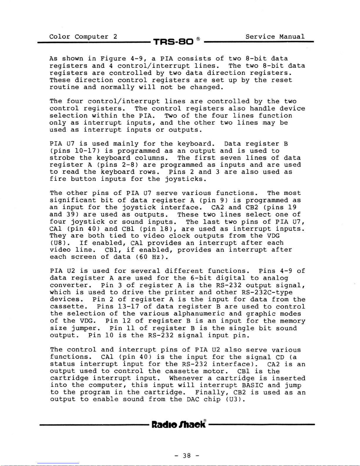
__
c_o_1_o_r_c_o_m_p_u_t_e_r_2
As
shown
registers
registers
These
routine
The
four
control
selection
only
used
PIA
U7
(pins
strobe
register
to
read
fire
The
other
significant
an
input
and
39)
four
CAl
They
video
each
(pin
(08).
in
Figure
and
are
direction
and
normally
control/interrupt
registers.
within
as
interrupt
as
interrupt
is
used
10-17)
the
keyboard
A
(pins
the
keyboard
button
are
joystick
are
If
line.
screen
inputs
pins
bit
for
used
40)
both
enabled,
of
____
4-9,
4
control/interrupt
controlled
control
will
The
the
PIA.
inputs,
inputs
mainly
is
programmed
columns.
2-8)
rows.
for
of
PIA
of
data
the
and
CBl,
or
tied
data
joystick
as
outputs.
sound
CBl
to
CAl
if
enabled,
(60
TRS-BO
a
by
registers
control
or
for
are
the
U7
serve
registe
inputs.
(pin
video
provides
Hz).
PIA
consists
lines.
two
data
are
not
be
changed.
lines
Two
and
outputs.
the
as
programmed
Pins
joysticks.
interface.
18),
clock
are
registers
of
the
the
other
keyboard.
an
output
The
These
first
2
various
-r A
The
are
outputs
an
provides
®
of
direction
set
controlled
four
as
and
3
functions.
(pin
CA2
two
last
used
interrupt
an
two
The
up
also
lines
two
Data
and
seven
inputs
are
9)
is
and
lines
two
as
interrupt
from
interrupt
Service
8-bit
two
8-bit
registers.
by
the
by
handle
function
lines
is
also
pins
after
may
register
used
lines
and
used
programmed
CB2
select
(pins
of
the
data
reset
the
to
of
are
The
one
PIA
inputs.
VDG
each
after
Manual
data
two
device
be
B
data
used
as
most
as
19
of
U7,
PIA
02
is
data
converter.
which
devices.
cassette.
the
of
size
output.
The
functions.
status
output
cartridge
into
to
output
register
is
selection
the
jumper.
control
the
the
used
used
Pin
VDG.
Pin
interrupt
used
interrupt
computer,
program
to
enable
Pin
Pins
Pin
10
and
CAl
to
for
A
are
3
to
drive
2
of
13-17
of
the
12
Pin
is
interrupt
(pin
input
control
in
sound
several
used
of
register
register
various
of
11
of
the
40)
input.
this
the
different
for
the
printer
A
of
data
register
register
RS-232
pins
is
for
the
the
cassette
Whenever
input
cartridge.
from
the
6-bit
A
is
the
and
is
the
register
alphanumeric
B
is
B
is
signal
of
PIA
the
input
RS-232
motor.
will
the
Finally,
DAC
interrupt
chip
functions.
digital
RS-232
other
input
B
an
the
input
02
for
interface).
a
cartridge
-----------llad1elhaell-----------
for
are
and
input
single
pin.
also
the
CB2
(03).
Pins
to
analog
output
RS-232C-type
data
used
graphic
for
serve
signal
CBl
BASIC
is
is
to
the
bit
is
used
from
various
CA2
the
inserted
and
4-9
signal,
the
control
modes
memory
sound
CD
(a
is
jump
as
of
an
an
- 38 -
Page 45

Color
Computer
-----------TRS-80
2
®
Service
Manual
4.7
ROM
that
power
fetch
were
the
haywire.
ROMs,
Color
programmed
and
component
installed,
all
paralleled
independent
is
4.8
PIA
Interface
outputs,
matrix.
connects
an
resistors
PIA
resistance
in
ROM
stands
retains
is
a
vector
no
ROM,
data
depending
Basic.
functions.
address
provided
Keyboard
U7
is
open-collector
compensates
a
highly
(Ul2
applied
bus,
and
The
to
and
for
its
the
attempt
The
Color
Each
to
provide
for
the
even
and
to
the
for
by
Interface
the
only
circuit.
connects
A
the
contained
due
reliable
Ul3)
Read
data
to
and
CPU
upon
Ul2
Extended
in
data
two
each
Ull,
side
row
device
for
to
prolonged
Only
when
the
CPU,
begin
would
to
Computer
whether
ROM
contains
the
contains
the
Extended
lines,
ROMs.
ROM
the
active
The
to
of
U7
lines
in
RPl.
a
possible
keyboard
74LS138,
CU7)
B
Memory,
power
it
executing
read
execute
2
contains
it
user
is
component
side
the
is
of
and
with
Standard
Basic
as
well
The
the
of
column
configured
the
as
The
increase
use,
interface.
which
is
immediately
random
this,
is
8K
ROM.
Basic
only
CE
as
this
keyboard
such
use
and
is
removed
instructions.
floating
and
either
Standard
bytes
certain
Basic,
Ul2
machine.
as
Vee
line
or
chip
appropriate.
in
the
PIA
lines
as
requires
of
an
in
therefore
a
type
from
attempts
promptly
or
which
Basic
must
and
that
enable
Keyboard
is
of
inputs,
matrix.
open-collector
key
of
states
one
Extended
are
and
always
Note
ground,
is
configured
the
the
contact
should
memory
it.
Ul3
keyboard
When
to
If
there
on
go
or
two
commands
is
be
that
are
line
pullup
and
PIA
which
U7
result
the
•
as
is
To
read
a
zero
writing
pressed
zero
low.
keys
in
and
By
may
the
keyboard,
the
ones
in
that
the
scanning
be
checked.
in
key
-----------ltadle
bit
all
column,
location
that
the
each
only
Figure
one
corresponds
other
one
of
will
column
4-10
-
column
bits.
the
correspond
in
the
to
If
input
keyboard,
shows
is
that
a
the
enabled
column
key
lines
to
the
keyboard
is
will
all
by
writing
and
being
be
bit
of
lhaell----------
39
-
by
a
that
the
matrix.
is
Page 46

Color
Computer
2
Service
Manual
-----------TRS-80
®
-----------
J5
I
I
I
I
I
5
,_____ _ ____,
61---~
71---~
81-------<
I
iQ}---NC
I
L
__
Figure
4-10.
Color
Computer
2
Keyboard
Array
-----------1tad1elhaell----------
- 40 -
Page 47

Color
Computer
------------TRS-BO
2
®
-----------
Service
Manual
4.9
'l'wo
Computer
including
RS-232
production/selection.
custom
2.
Converter.
the
controllers
block
The
Six
discrete
sound
reference
of
attenuated
data
There
B.
compared
coupled
table:
DAC
special
serial
linear
As
its
circuitry
diagram
DAC
bits
inputs
the
four
storage.
are
These
Circuitry
analog
2
to
power
name
This
to
itself
of
control
internal
for
joystick
and
two
determine
against
to
the
to
(03)
integrated
implement
supply
interface,
integrated
implies,
chip
necessary
the
microprocessor.
of
the
performs
are
analog
the
sound
a
comparator,
used
select
sound
as
which
the
a
multitude
regulation,
the
The
circuits
it
also
to
DAC
chip.
most
used
level.
multiplexer.
inputs.
the
inputs
DAC,
output
as
circuits
joystick
DAC
contains
contains
interface
of
by
the
Finally,
cassette
to
of
the
well
pin
of
cassette
chip
used
the
the
This
other
the
DAC
joystick
as
according
are
analog
interface,
(03)
a
Figure
functions
DAC
recording
in
a
Digital
sound
the
to
level
It
input
the
chip:
which
is
the
joystick
used
functions
operation,
one
Color
to
multiplexer
4-11
of
specify
is
one
is
also
of
which
DAC
signal
signal
Sel
inputs
sound
to
the
in
the
and
of
the
Computer
Analog
shows
this
a
of
used
A
and
is
to
source
following
Color
the
sound
and
a
chip.
the
as
is
one
is
for
Sel
be
is
a
Sel
0
0 1
1
1
The
Digital
transistor
over
position
technique
microprocessor
means
the
of
entire
of
the
B
to
as
the
called
select
Sel
A
0
0
1
Analog
a
current
voltage
joystick,
"Successive
first
Joystick
Converter
range.
selects
pins
Joy
Joy
Joy
Joy
sourc~
the
(which
which
microprocessor
Approximation".
the
Input
0
1
2
3
employs
In
order
desired
are
connected
gives
----------llad1elhaell----------
a
64-collector
good
to
determine
uses
joystick
Sound
linearity
The
to
PIA
Source
DAC
cassette
Cartridge
(no
sound)
the
a
input
07).
by
-
41
-
Page 48

Color
Computer
2
Service
Manual
-----------TRS-80
®
-----------
Vee®
ANALOG
INPUTS
@0------1
@0------1
@0------1
@~-
@
@
ANALOG
SELECT
WEIGHTED
CURRENT
SOURCES
DO
@
D1
@)
CURRENT
SWITCH
D2
®
AND
D3
®
1/V
CONVERTER
D4
-
DS
(j)
-
®
BUFFER
@
CASSO
UT
COMPARATOR
SELECT
ANALOG
CD
LOGIC
SWITCH
SOUND-OUT
fl
SND
SND
SND
ENABLE
I
II
@
®
@)
@
Figure
4-11.
DAC
Block
Diagram
-----------nad1elhaell-----------
-
42
-
Page 49

Color
Computer
-----------TRS-BO
2
®
-----------
Service
Manual
Next,
range,
input
the
(comparator
higher,
was
between
pin
between
value,
value
found.
DAC
one
DAC
controllers.
The
the
Sel
the
microprocessor
six
waveshape.
attenuated
the
volume.
from
This
which
volume
the
Similarly,
pin
AC-coupled,
input
is
in
a
value
32
via
joystick
the
low,
0
was
high,
the
the
of
Since
settings
axis
chip
sound
above
A
and
sound
bits
level
the
level
point
control
level
8
of
at
3.9
volts
clipping
decimal
PIA
the
and
the
of
correspond
multiplexing
table,
Sel
output.
of
required
If
cassette
which
the
the
equivalent
for
U2.
voltage,
output)
HI/LO
next
the
the
last
microprocessor
preceding
the
are
the
B
the
The
to
provide
the
follows
it
the
cartridge
since
midpoint
p-p.
(distortion)
If
is
pin
value
last
microprocessor
value
DAC
required
joystick.
to
different
inputs,
If
simply
DAC
output
clips
on
provides
cartridge
in
by
cassette
recorder
the
the
the
the
Any
to
the
example,
the
DAC
the
HI/LO
low.
is
high
the
value,
and
either
difference,
uses
to
two
section
and
the
DAC
feeds
order
of
the
approximately
the
modulator
is
input
input
cassette
3.9
may
connector).
SND
of
input
the
greater
of
is
output
However,
(logic
microprocessor
or
64,
or
six
binary
determine
The
four
axes
is
sound
the
is
a
succession
to
DAC
the
is
routed
level
waveform.
should
volts
supply
allowable
signal
the
midpoint
sent
voltage
pin
of
one).
16
decimal.
tries
48
decimal.
adds
until
joystick
for
each
very
sources
selected
used
produce
is
then
3.9
to
selected
to
up
p-p
the
This
to
the
sound
of
the
to
the
the
DAC
if
the
DAC
If
tries
a
value
or
subtracts
the
digits,
the
"position"
of
two
simple.
are
input
as
a
sound
of
values
the
desired
buffered
volts
produce
input,
the
sound
to
3.9
Therefore,
not
be
to
the
sound
signal
DAC
chip
voltage
amplitude
waveform.
voltage
DAC's
is
lower
chip
voltage
the
is
If
the
half-way
For
final
exactly
inputs
joystick
According
selected
is
routed
source,
p-p,
maximum
then
output.
volts
set
higher
DAC
chip.
source
may
biases
swing,
will
six-bit
than
HI/LO
half-way
HI/LO
each
half
value
six
along
to
the
by
to
the
and
which
sound
p-p,
the
(from
be
the
which
result
is
pin
the
is
to
the
to
the
is
at
than
In
addition
by
bringing
by
PIA
single
U2.
bit
to
SNDEN
If
sound)
-----------1tad1e
the
this
Select
to
pin
is
inputs,
a
high
is
disabled.
level.
at
a
the
low
sound
This
level,
must
input
all
lhaell----------
-
43
-
be
is
controlled
sound
enabled
(except
Page 50

____
c_o_1_o_r
The
signal
simply,
produce
Therefore,
necessary
software.
__
c_o_m_p_u_t_e_r
final
function
for
recording
a
buffered
approximately
it
FSK
___ 2 _________
of
the
of
output
1
is
up
to
signals
through
"TFl!3-E3Cl
DAC
chip
cassette
of
the
volt
the
p-p
microprocessor
the
®
is
data.
DAC
into
DAC
___________
to
provide
This
which
a
2K
to
and
the
s_e_r_v_1_·c
is,
is
attenuated
ohm
load.
produce
proper
__ e __
the
quite
M_a_n_u_a_1
output
the
__
to
4.10
The
responsible
translation,
cassette
4-12.
Figure
voltage
through
provides
Color
this
and
wave
is
voltage
is
output
else
CR3
positive
C2.
pass
16.
to
current
through
by
keep
capacitors
power
SALT
SALT
4-13
Computer
AC
to
the
center-tapped
filtered
internally
drivers.
in
and
This
transistor
The
+5
VDC
pin
3
the
supply.
Circuitry
chip
for
relay,
shows
is
brought
fuse
17.2
voltage
anodes
by
is
then
the
computer.
CR4
form
output
positive
SALT
and
for
the
resistor
of
the
voltage
CS
Ul
(Supply
supply
cassette
as
the
Fl.
The
VAC,
2
circuit
is
of
electrolytic
applied
regulated
The
a
which
Ql
chip
provides
computer
R2.
SALT
at
and
Cll
(Ul)
and
regulation,
read
is
shown
complete
into
secondary
center-tapped,
applied
CR3
rectifier
negative
full
is
voltage
and
internally
The
chip
a
steady
are
the
board.
and
to
to
wave
filtered
is
the
is
used
voltage
and
used
operations,
in
primary
to
capacitor
pin
-5
is
base
drawn
Level
the
CR4.
with
VDC
voltage
center-tapped
applied
regulates
the
+5 voe,
the
power
of
at
If
cathodes
a
15
of
and
by
to
power
drive
from
at
base
to
prevent
Translator)
RS-232
block
supply
of
the
1.8
switch
CRl
negative
the
electrolytic
this
+/-
interface
and
driving
diagram
circuit.
transformer
power
amps
Sl
of
and
CR2
Cl.
used
is
to
current
SALT
not
the
the
the
the
point
drive
5%.
oscillation
This
for
rectifier
SALT
positive
emitter
is
level
the
in
Figure
Tl
transformer
RMS
CRl
output.
used
collector
adjusted
to
is
closed,
and
form
chip,
the
for
Electrolytic
a
negative
where
RS-232
anywhere
capacitor
chip
Ql.
of
is
monitored
AC
the
CR2,
full
This
with
of
at
pin
voltage
The
Ql
to
of
the
it
a
---------------------nat11elhaell---------------------
-
44
-
Page 51

Color
Computer
2
-----------TRS-BO
®
UNREGULATED
+ V INPUT
Service
Manual
+ S VOLT
~1--..{>
PASS TRANSISTOR BASE DRIVE
REGULATOR
2
PASS TRANSISTOR CURRENT SENSE
DRIVER
L
____
_J;;..
3
---<
CURRENT LIMIT
8
UNREGULATED
-V
INPUT
15
REGULATED - 5 VOLTS
- 5 VOLT
~---C>
REG (INTERNAL TO SALT ONLY)
8
TIL
INPUT
[>
12
FOR RS-232C
)>--------
6
-t
>------C>
RS-232C OUTPUT
OUTPUT
~----~14[>~-----4~~
~
/ >
~
RS-232C
TIL
OUTPUTS
INPUTS
I
"'
>
13[>
5
t>
CASSETIE
DATA
..__
______
11-t[>..__
_____
1__,.._
TIL
OUTPUT
(ZERO
CROSSING>-
·
.-
_..
INPUT)
_______
9
___,C>
RELAY DRIVE OUTPUT
10~
TIL
INPUT
)>--------1~
-
Figure
4-12.
SALT
Block
Diagram
----------1tad1elhaell----------
-
45
-
Page 52

__
c_o_1_o_r_c_o_m_p_u_t_e_r_2
____
TRS-BO
®
01
Service
R2
.1 1/2W
Manual
F1
3/10 A S.B.
The
SALT
from
as
will
reducing
the
in
the
"fold
T1
Figure
chip
supply
case
back"
the
51
cgd:
.02
4-13.
senses,
through
of
base
T .02
_+:J
a
short
the
drive
C1
:jT'220
..J_ 16V
C7
Color
at
pin
Rl.
voltage
current,
µF
Computer
2,
If
or
component
output
the
amount
excessive
of
thus
protecting
1
U1
SALT
IC
2
Power
failure,
the
2
3
Supply
of
current
current
supply
R1
51
the
the
is
by
drawn
drawn,
SALT
supply.
+ cs,
100µF
I
11
16V
Ferrite
ClO,
might
There
SALT
level
from
approximately
This
the
current
SALT
shorted
may
serve
be
are
chip
converter
PIA
output
output
chip
be
present
beads
to
present
two
for
U2,
connector.
drawn
if
to
an
FBl
decouple
types
use
inverts
+5
is
coupled
from
the
external
on
takes
VDC
-----------
and
on
the
of
with
this
output
some
FB2,
as
it,
for
as
and
prevent
DC
supply
Level
the
RS-232
its
and
a
space
through
R3
serves
output
Cat
voltage
RS-232
well
from
Translators
interface.
input
uses
the
it
and
a
270
to
and
connector)
(such
connectors).
as
capacitors
any
digital
entering
a
standard
to
-5
ohm
limit
prevent
as
contained
drive
VDC
+/-
for
resistor,
the
damage
is
12
ltadtelhaell----------
-
46
-
C7
through
"noise"
the
AC
in
the
The
output
TTL
signal
the
output
a
mark.
R3,
amount
inadvertently
VDC,
to
of
the
which
which
line.
to
to
Page 53

__
c_o_1o_r_c_o_m_p_u_t_e_r_2
____
TRS-BO
®
Service
Manual
The
input
incoming
These
voltages
negative
positive
task
4-14
and
for
(resistor/zener
CR6
voltages
incoming
less
than
greater
or
mark
compatible
The
cassette
composed
input
R23,
from
then
resistor,
output
and
damage
characteristic
R4
limits
to
voltage
Shack's
circuitry
p-p.
The
changes
level
RS232
voltage
voltage
the
SALT
(as
shown
and
prevent
signals
that,
than
is
that,
then
level,
loading
of
a
zero-crossing
the
coupled
R4.
the
the
SALT
is
fed
CCR-81
is
protected
zero-crossing
state
each
converters
voltage
are
defined
between
between
chip,
in
are
they
they
output
and
cassette
into
R23
serves
current
chip
into
does
the
not
time
have
levels
as
-3
+3
either
diode
the
them
combination)
PCB
from
compared
are
considered
are
from
is
coupled
circuitry
being
the
SALT
to
of
most
of
if
an
cassette
produce
from
detector
the
the
to
standard
follows:
and
-25
and
+25
the
schematic)
reaching
to
a
considered
the
SALT
into
internal
detector.
loaded
chip
load
the
portable
the
incoming
excessively
input.
more
voltages
internal
incoming
task
VDC;
VDC.
circuit
reference
to
of
a
a
To
or
clamp
the
be
a
a
space.
chip
PIA
to
Figure
by
a
through
converting
TTL
signals.
"mark"
"space"
simplify
shown
series
the
SALT
of
mark.
at
an
U2.
the
4-14
220
ohm
a
capacitively-coupled
cassette
signal
large
Although
than
as
signal
6
high
to
volts
as
the
passes
is
a
is
a
the
in
Figure
diodes
negative
chip.
2.0
VDC.
If
The
space
LS
TTL
SALT
chip
shows
resistor,
510
ohm
recorders,
to
prevent
peak-to-peak
Radio
p-p,
18
volts
SALT
through
CR5
The
If
is
the
the
TO PIA U2-2
TO PIA U2-10
TO PIA U2-40
FROM
PIA
U2-3
-----------
R4
1K
510
-
-=-
I/O
3.9V
ZENER
3.9V
ZENER
Circuitry
RS-232C
DATA
INPUT
RS-232C
CD INPUT
-=-
Figure
11
14
13
12
1K
R3
270
4-14.
7
4
U1
SALT
5
6
l.C.
CASSETTE DAT A
(ZERO CROSSING)
INPUT
R23
220 1/2W
RS-232C
DATA OUT
aM11elhaell-----------
- 47 -
Page 54

Color
Computer
-----------TRS-BO
2
®
Service
Manual
zero
which
of
crossing
coupled
The
relay.
chip
Darlington
The
to
relay
the
cassette
When
There
of
relay
collapsing
damaging
4.11
volts.
provides
the
zero-crossing
final
where
collector
one
end
connects
transistor
the
is
the
relay,
coil
Cassette
detector
into
function
A TTL
it
transistor,
of
relay
incoming
no
ground
is
magnetic
the
There
noise
is
PIA
U2.
signal
is
connected
exits
the
cassette
to
+SV.
becomes
to
ground,
signal
so
it
to
prevent
transistor
Tape
is
a
immunity
detector.
an
of
the
from
the
the
saturated
return
is
de-energized.
field
Format
small
LS TTL
SALT
PIA
to
emitter
SALT
When
in
chip
relay.
the
causing
is
low,
for
the
counter-emf
(when
the
Information
amount
and
prevents
The
output
compatible
chip
U2
the
the
SALT.
is
enters
base
of
at
The
incoming
and
the
the
+S
the
relay
of
hysteresis
of
level
to
drive
pin
of
an
which
pin
9,
other
signal
connects
relay
transistor
volts
The
diode
caused
de-energizes)
false
the
10
internal
is
and
end
its
to
at
the
built
triggering
zero-
and
is
the
cassette
of
the
grounded.
is
connected
of
the
goes
end
energize.
is
cut
other
across
by
the
SALT
high,
of
off.
end
the
from
in
the
The
standard
following
1.
2.
3.
4.
S.
6.
The
block
of
File
1.
2.
3.
4.
S.
6.
7.
items:
A
A
A
second
the
A
One
An
format
block
One
One
One
One
Data
One
plus
One
TRS-80
leader
Namefile
blank
second
End
section
in
Namef
or
more
of
for
is
as
leader
sync
block
OlH =
FFH = End
OOH = Namef
block
--
0
checksum
block
trailer
Color
consisting
block
length
ile
leader
Data
File
follows:
byte
type
length
to
block
Data
byte
-byte:
Data
of
2SS
byte
type
byte
Computer
of
of
tape
to
allow
of
128
blocks
blocks,
--
SSH
3CH
block
File
ile
block
byte
bytes
and
--
--
--
the
block
SSH
2
tape
128
bytes
equal
BASIC
bytes
Namefile
block
OOH
sum
length
is
of
to
approximately
time
of
SSH
blocks,
to
FFH
of
all
bytes
composed
SSH
to
evaluate
or
the
data
of
an
bytes
the
1/2
End
-----------
ltad1elllaell----------
- 48 -
Page 55

__
c_o_1_o_r_c_o_m_p_u_t_e_r_2
The
End
of
File
0.
The
Namefile
bytes
BASIC
(OFH).
and
are
____
block
block
The
15
employed
is
TRS-BO
is
a
a
standard
bytes
as
standard
of
data
described
®
block
block
provide
below:
with
with
Service
a
length
a
length
information
Manual
of
of
15
to
1.
2.
3.
4.
5.
6.
4.12
The
RS-232C
interface
with
capable
signals
printers,
1.
2.
3.
4.
Eight
One
One
One
Two
language
Two
language
RS-232
allows
of
used
CD
RS232IN
GROUND
RS2320UT
bytes
file
OOH
OlH =
02H =
ASCII
Gap
flag
bytes
bytes
Connector
interface
the
modems,
interfacing
by
the
for
type
= BASIC
program
program
byte:
Data
Machine
flag
for
for
interface
byte
byte
the
the
(J3)
utilizes
computer
other
with
a
serial
zero
serial
the
program
Program
File
Code
--
-start
load
to
computers,
RS-232C
are:
status
voltage
Program
OOH=
OlH =
address
address
a
4-pin
have
line
data
data
name
Binary,
continuous,
of
of
DIN
serial
or
signals.
input
reference
out
FFH
=
FFH =
a
machine
a
machine
connector.
communications
any
device
The
four
ASCII
gaps
This
The
the
pinout
computer)
for
Figure
----------
is
the
shown
RS232
DIN
connector
in
Figure
OUT~
v-
4-15.
RS-232C
lladtelllaell----------
-
(viewed
4-15.
CD
RS2321N
Connector
49
-
from
Pinout
the
rear
of
Page 56

Color
Computer
-----------TRS-BO
The
RS232C
capable
with
possible
signals
be
correct
In
Basic
the
the
the
accomplished
software,
ROM
pin
above
interface
of
communicating
minimum
that
may
be
high
is
assignment
description:
2
three-signal
devices
used
by
or
low
the
only
a
serial
hardware
with
which
with
connecting
level.
of
the
RS-232C
printer.
the
connector
in
any
interface.
use
a
Color
unused
device
For
®
the
Color
device
larger
Computer
device
supported
use
differs
Computer
which
It
set
with
Service
will
is
also
of
RS-232C
2.
This
inputs
by
the
slightly
2
operate
would
to
the
printer,
from
Manual
is
the
8K
1.
2.
3.
4.
If
your
must
This
time.
In
order
assumptions
Some
modified.
variables
printer
be
connected
tells
1.
2.
3.
4.
5.
printers
No
Connection
Connected
the
printer
Ground
Connected
the
computer
to
operate,
about
The
printer
The
printer
The
printer
The
printer
at
the
feed
The
two
or
at
data
stop
will
This
by a special
does
to
the
end
this
may
to
the
to
the
not
a
positive
that
the
printer.
operates
width
generates
will
of
the
time.
format
bits,
require
be
accomplished
BUSY
Serial
provide
software
automatically
is
and
that
driver
the
is
line.
one
no
output
voltage
These
at
132
a
parity.
these
Data
a
status
printer
must
600
columns.
BUSY
It
start
by
routine.
(or
status
Input
of
make
assumptions
Baud.
when
will
bit,
assumptions
changing
line,
+3
is
ready
several
it
return
also
eight
of
line)
the
then
to
+12
all
are:
is
not
the
do a line
data
be
RAM
of
printer
pin
2
volts.
of
the
ready.
carriage
bits,
-----------1tad1elllaell-----------
- 50 -
Page 57

Color
Computer
------------TRS-80
A
list
Also,
variables.
equal
comma
of
Table
to
the
field
all
2
The
width
2
the
lists
last
width
printer
some
comma
value
will
variables
alternate
field
minus
normally
variable
the
stay
®
-----------
is
values
comma
at
given
for
should
field
16.
Service
in
Table
these
width.
be
Manual
1.
set
The
4.13
The
expanding
All
Cartridge
40-pin
of
the
cartridge
the
important
connector.
signals
VARIABLE
BAUD RATE
BAUD
LINE
LINE
COMMA
LAST COMMA
LINE PRINTER WIDTH
is
RATE
DELAY
DELAY
FIELD
provided
MSB
LSB
MSB
LSB
WIDTH 0099
FIELD
TRS-80
A
complete
Connector
connector
Color
CPU
in
HEXIDECIMAL
ADDRESS ADDRESS DECIMAL
0095
0096
0097
0098
000A
0098
(J6)
bus
list
Table
provides
Computer
signals
and
brief
3.
DECIMAL
149
150
151
152
153
154
155 84 132
the
2
in
almost
are
tied
description
possibility
HEXI-
any
manner.
to
this
of
these
INITIAL
00 0
57
00 0
01
10 16
70
VALUE
DECIMAL
87
112
of
1
----------lladlOlhaell----------
Table
1.
Line
Printer
-
51
variables
-
Page 58

Color
Computer
-----------TRS-80
2
®
Service
Manual
BAUD
300 BAUD
600 BAUD
2400 BAUD
.288 SECONDS
.576 SECONDS
WIDTH:
32
64 CHARACTERS/LINE
255 CHARACTERS/LINE
RATE:
120 BAUD
1200 BAUD
LINE
DELAY:
1.15SECONDS
16
CHARACTERS/ LINE 16
CHARACTERS/ LINE
DECIMAL
MSB
DECIMAL
MSB
128
255
DECIMAL
VALUE
LSB
1 202
0
0
0
0
64
180
87
41
18
VALUE
LSB
0
0
255
VALUE
32
64
255
HEXIDECIMAL
MSB
01
00
00
00
00
HEXIDECIMAL
MSB
40
80
FF
HEXIDECIMAL
10
20
40
FF
VALUE
LSB
CA
BE
57
29
12
VALUE
LSB
00
00
FF
VALUE
Table
2.
Alternate
-----------
Line
Printer
variable
Values
llad1elhaell----------
-
52
-
Page 59

__
c_o_1_o_r_c_o_m_p;..u_t_e_r_2
____
TRS-BO
®
Service
Manual
PIN
#
SIGNAL
NAME
DESCRIPTION
1 N/C
2
N/C
3
HALT*
Halt
Input
to
the
CPU
4
NMI*
Non-Maskable Interrupt
to
the CPU*
5 RESET*
Main
Reset
And Power-Up Clear Signal
To The System
6 E
Main
CPU
Clock (0.89 MHz)
7
Q
Quadrative
Clock Signal Which
Leads
E
8
CART*
Interrupt Input For Cartridge
Detection
9
+5V
+5 Volts (300 MA)
10
D0
CPU
Data
Bit
0
11
Dl
CPU
Data
Bit
1
12
D2
CPU
Data
Bit
2
13
D3
CPU
Data Bit 3
14
D4
CPU
Data
Bit
4
15
D5
CPU
Data
Bit
5
16
D6
CPU
Data
Bit
6
17
D7
CPU
Data
Bit
7
18
R/W*
CPU
Read
- Write Signal
19
A0
CPU
Address
Bit
0
20
Al
CPU
Address Bit 1
21
A2
CPU
Address
Bit
2
22
A3
CPU
Address Bit 3
23
A4
CPU
Address
Bit
4
24
A5
CPU
Address
Bit
5
25
A6
CPU
Address Bit 6
26
A7
CPU
Address Bit 7
27
AS
CPU
Address
Bit
8
28
A9
CPU
Address
Bit
9
29
A10
CPU
Address
Bit
10
30
Al
1
CPU
Address
Bit
11
31
A12
CPU
Address
Bit
12
32
CTS*
Cartridge Select Signal
33 GND
Signal Ground
34
GND
Signal Ground
35
SND
Sound
lnout
36
scs*
Spare
Select Signal
37
A13
CPU
Address
Bit
13
38 A14
CPU
Address
Bit
14
39
A15
CPU
Address
Bit
15
40
SLENB*
Input
To
Disable Device Selection
Table
3.
Cartridge
Connector
Signals
----------1tad1elhaell----------
-
53
-
Page 60

Color
Computer
-----------TRS-80
The
most
ROM
cartridge.
connected
interrupt
computer
In
addition
several
the
Cartridge
common
to
anytime
to
DO
APPLIED
control
2
use
For
the
cartridge
jump
to
to
NOT
TO
DAMAGE
the
and
connector.
of
the
Cartridge
the
cartridge
the
program
PLUG
A CARTRIDGE IN
THE
COLOR
TO
·rHE UNI'r AND/OR
CARTRIDGE
expected
special
cartridge
detection,
interrupt
is
in
CAUTION
COMPUTER 2 AS
MAY
RESULT.
data,
purpose
They
address,
are
®
connector
pin,
plugged
ROM.
WITH
signals
as
follows:
the
which
in
POWER
SERIOUS
THE
and
are
Service
is
Q
clock
generates
and
R/W
available
with
is
forces
lines,
Manual
the
an
the
on
HALT*
HALT
current
processor
mode,
and
any
NMI*
RESET*
signal.
E,
CART*
to
CTS*
when
Hex,
not
SND
of
signals
should
--
state
making
ROM.
loss
--
Q
--
detect
-the
as
active
--
the
This
immediately
instruction.
address
The
of
This
--
This
These
--
This
the
This
processor
long
during
This
DAC
chip,
to
be
be
AC
active
it
possible
processor
internal
is
the
is
are
is
an
presence
is
the
as
the
signal
fed
coupled,
low
following
While
and
data
data.
non-maskable
the
master
the
two
interrupt
of
Cartridge
reads
SAM
a
write
is
connected
and
allows
through
and
signal
for
may
clock
a
any
is
to
the
should
lines
in
places
the
in
the
are
external
be
HALTed
interrupt
system
signals
input
cartridge.
Select
location
Map
these
directly
cartridge-generated
TV
sound
not
the
execution
HALTed
in
devices
indefinitely
reset
into
Signal.
from
Type
0.
locations.
system.
exceed
processor
state,
the
input
and
for
PIA
COOO
Note
to
of
the
the
high
the
the
3.9
impedance
to
access
without
to
power-up
MC6809E CPU.
U2.
It
It
is
Hex
that
sound
sound
The
volts
in
the
clear
is
valid
to
FEFF
it
input
signal
p-p.
a
RAM
CPU.
used
is
-----------
llad1e
-
lhaell----------
54
-
Page 61
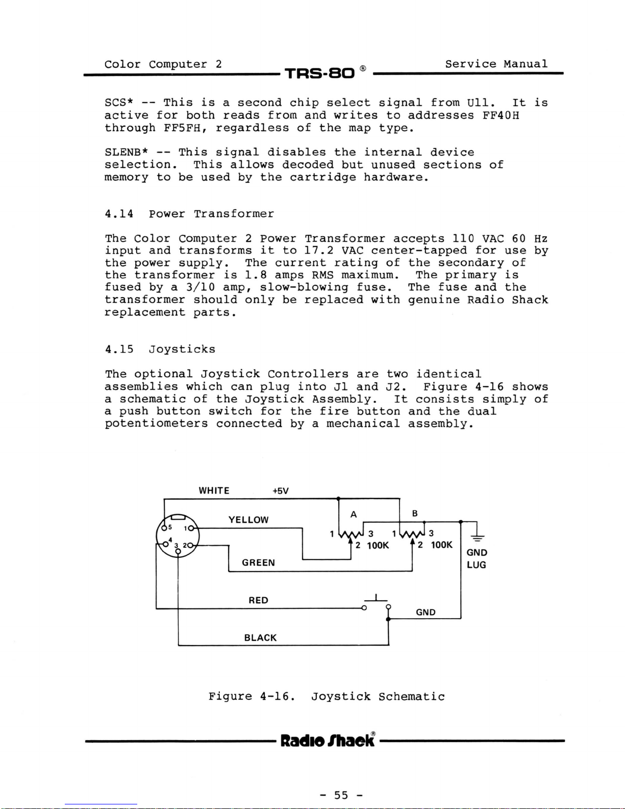
Color
Computer
-----------TRS-80
2
®
Service
Manual
SCS*
active
through
SLENB*
--
This
for
FF5FH,
--
selection.
memory
4.14
The
input
the
the
fused
to
Power
Color
and
power
transformer
by
a
transformer
replacement
4.15
The
Joysticks
optional
assemblies
a
schematic
a
push
button
potentiometers
is
a
both
reads
regardless
This
be
This
used
signal
allows
Transformer
Computer
transforms
supply.
is
3/10
amp,
should
parts.
Joystick
which
of
the
switch
connected
second
from
disables
by
the
2
Power
it
The
1.8
slow-blowing
only
Controllers
can
plug
Joystick
for
chip
of
and
select
writes
the
map
the
decoded
but
cartridge
Transformer
to
17.2
current
amps
be
replaced
into
RMS
Jl
VAC
rating
maximum.
Assembly.
the
fire
by a mechanical
signal
to
addresses
type.
internal
unused
hardware.
accepts
center-tapped
of
the
fuse.
with
are
and
The
genuine
two
J2.
It
button
and
assembly.
from
device
sections
110
secondary
The
primary
fuse
identical
Figure
consists
the
Ull.
FF40H
of
VAC
for
and
Radio
4-16
simply
dual
It
60
use
of
is
the
Shack
shows
is
Hz
by
of
WHITE +5V
YELLOW
Figure
GREEN
RED
BLACK
4-16.
Joystick
A
3 1
100K
Schematic
-----------1tad1elhaell----------
B
GND
3
100K
GND
LUG
-
55
-
Page 62

Color
computer
-----------TRS-80
The
mechanical
changed
two-dimensional
so
that
variable
This
the
a
momentary
at
a 5
allows
handle
the
resistor,
is
2
assembly
same
control.
volt
the
center
moved.
ground
time.
reference
and
ground
wiper
The
contact
allows
This
The
potentiometers
is
applied
is
to
push-button
for
®
both
gives
connected
vary
an
input
Service
potentiometers
the
effect
are
to
one
side
to
the
from
0
switch
signal.
to
merely
to
of
connected
of
other.
5
volts
Manual
be
a
the
as
provides
4.16
The
with
TV
the
TV
computer
the
schematic
TV
antenna
connectors
antenna,
customer's
antenna
phone
INPUT
COMPUTER
Switch
is
output
plug
of
FROM
Box
switch
and
attached
the
box
provided
the
TV
through
is
connected
input
antenna
home TV.
on
,----
1
I
I
I
I I
L
_______
BALUN
consists
for
the
directly
the
switch
switch
of
attachment
The
switch
300
ohm
to
through
box.
j
a
switch
twin-lead
the
a
box.
60 dB
SWITCH
I I
to
the
box
switch
75
ohm
Figure
I
and
computer,
is
box.
coax
a
balun,
connected
output.
The
cable
4-17
shows
TWIN LEAD OUTPUT
TO
THE
the
to
The
to
a
TV
ATTENNA
300
INPUT
ohm
>>-,_-------------'V"'
----~~~~~~~~-r-u~'
>
Figure
From
switch
inpedance
signal
specially
required
the
box
is
computer,
which
to
then
designed
between
-----------ltadle
4-17.
matches
a
TV's
connected
the
the
signal
300
to
provide
computer
Antenna
the
modulator's
ohm
antenna
to
the
-
J
~-'-~~o
Switch
is
connected
switch.
the
60
and
the
lhaell----------
56
-
Box
input
dB
TV
Schematic
to
75
ohm
impedance.
The
switch
of
isolation
antenna.
a
balun
output
is
in
This
the
Page 63

Page 64

Page 65

Page 66

Page 67

Page 68

Color
Computer
-----------TRS-BO
2 ®
"
-----------
Service
Manual
Main
Logic
PCB
#8857625
(8857636*),
Color
Computer
2
=======================================================
Item
Ref
Description
Part
Number
=======================================================
1 1
2
3
4
5 2
6
7
8 1
9 1
10
11
CAPACI'rORS
1
9
3
5
1
2
1
Cl
C2
C3
C4
cs
CG
C7
ca
C9
ClO
Cll
Cl2
Cl3
Cl4
Cl5
Cl6
Cl7
Cl8
Cl9
C20
C21
C22
C23
C24
C25
C26
C27
PCB,
Lug,
Socket,
Socket,
Socket,
Socket,
Switchcap
Bracket,
Heats
Nut,
Label,
220
4700
0.1
0.1
100
0.1
0.02
0.02
0.02
0.02
100
N.A.
0.02
0.02
0.1
0.02
0.02
0.1
0.1
10
0.1
0.02
0.02
0.1
0.1
0.001
0.02
Main
Fast-On
U22,23)
ink,
#6 KEPS
mfd,
mfd,
mfd,
mfd,
mfd,
mfd,
mfd,
mfd,
mfd,
mfd,
mfd,
mfd,
mfd,
mfd,
mfd,
mfd,
mfd,
mfd,
mfd,
mfd,
mfd,
mfd,
mfd,
mfd,
mfd,
mfd,
Logic
16-Pin
20-Pin
24-Pin
40-Pin
(Reset)
Switch
6015-PBSEl
PCB
Serial
16V
16V
50V
50V
16V
50V
50V
50V
50V
50V
16V
50V
50V
50V
50V
50V
50V
50V
25V
Elec
50V
50V
50V
50V
50V
50V
50V
DIP(Ul,14-21)
DIP(U3,5,6)
DIP(Ul2,13)
DIP(U2,7,8,
(Reset)
Elec
Mono
Mono
Elec
Mono
Elec
Mono
Mono
Mono
Mono
Mono
Mono
Elec
Cer
Cer
Cer
Cer
Cer
Cer
Cer
Cer
Cer
Cer
Poly
Cer
Rad
Rad
Axial
Axial
Rad
Axial
Disk
Disk
Disk
Disk
Rad
Disk
Disk
Axial
Disk
Disk
Axial
Axial
Rd
Axial
Disk
Disk
Axial
Axial
Disk
NP
(Ql)
8709416
8529016
8509003
8509009
8509001
8509002
8489066
8729223
8549016
8579004
8789963
8327221
8328471
8374104
8374104
8327101
8374104
8303223
8303223
8303223
8303223
8327101
8303223
8303223
8374104
8303223
8303223
8374104
8374104
8396101
8374104
8303223
8303223
8374104
8374104
8352104
8303223
*Extended
Basic
-----------lladtelhaell----------
PCB
Number
-
67
-
Page 69

__
c_o_1o_r_c_o_m_p_u_t_e_r_2
____
TRS-BO
®
______
s_e_r_v_i_c_e_M_a_n_u_a_l_
Main
Logic
PCB
#8857625
(8857636*),
Color
Computer
2
=======================================================
Item
Ref
Description
Part
Number
=======================================================
CAPACITORS
C28
C29
C30
C31
C32
C33
C34
C35
C36
C37
C38
C39
C40
C41
C42
C43
C44
C45
C46
C47
C48 1
C49
cso
CSl
C52
C53
C54
C55
C56
C57
C58
C59
C60
C61
C62
(cont'd)
mfd,
0.1
0.1
mfd,
mfd,
0.1
N.A.
mfd,
0.1
mfd,
0.1
0.1
mfd,
mfd,
0.1
0.1
mfd,
pfd,
~3
pfd,
56
pfd,
56
0.1
mfd,
N.A.
N.A.
9-35
39
pfd,
0.1
mfd,
10
mfd,
0.1
mfd,
mfd,
N.A.
mfd,
0.1
mfd,
0.1
mfd,
0.1
mfd,
0.1
mfd,
0.1
mfd,
0.1
mfd,
0.1
mfd,
0.1
mfd,
0.1
pfd,
150
pfd,
33
150
pfd,
10
mfd,
pfd
sov
sov
sov
50V
50V
50V
sov
SOV
SOV
50V
SOV
SOV
Trimmer
SOV
SOV
25V
50V
SOV
sov
sov
sov
sov
sov
sov
sov
50V
sov
SOV
SOV
SOV
25V
Mono
Mono
Mono
Mono
Mono
Mono
Mono
Mono
Cer
Cer
Cer
Mono
Cer
Mono
Elec
Mono
Elec
Mono
Mono
Mono
Mono
Mono
Mono
Mono
Mono
Mono
Cer
Cer
Cer
Elec
Axial
Axial
Axial
Axial
Axial
Axial
Axial
Axial
Disk
Disk
Disk
Axial
Disk
Axial
Rad
Axial
Rad
Axial
Axial
Axial
Axial
Axial
Axial
Axial
Axial
Axial
Disk
Disk
Disk
Rad
8374104
8374104
8374104
8374104
8374104
8374104
8374104
8374104
8300334
8300564
8300564
8374104
8360356
8300394
8374104
8326102
8374104
8325104
8374104
8374104
8374104
8374104
8374104
8374104
8374104
8374104
8374104
8301154
8300334
8301154
8326102
CONNECTORS
J3
J4
Jl
J2
JS
JG
4-Pin
5-Pin
6-Pin
6-Pin
Keyboard
40-Pin
DIN
DIN
DIN
DIN
Right
Angle
lladle lhaell
-
68
-
8519094
8519085
8519095
8519095
8519176
8519139
Page 70

__
c_o_1_o_r_c_o_m
....
p._u_t_e_r_2
____
TRS-BO
®
_____
s_e_r_v_i_c_e_M_a_n_u_a_l_
Main
=====================================================~==
Item
Logic
Ref
PCB
#8857625
Description
(8857636*),
Color
Computer
Part
Number
2
========================================================
DIODES
CRl
CR2
CR3
CR4
CRS
CR6
CR7
CR8
CR9
CRlO
CRll
CR12
CR13
FBl
FB2
FB4
FB7
1N4002,
1N4002,
1N5401,
1N5401,
1N4148
1N4148
1KF20-04
1KF20-04
1N4148
1N4148
1N4148
1N4148
1KF20-04
Ferrite
Ferrite
Ferrite
Ferrite
sov,
sov,
lOOV,
lOOV,
Bead
Bead
Bead
Bead
lA
lA
3A
3A
8150002
8150002
8160401
8160401
8150148
8150148
8160020
8160020
8150148
8150148
8150148
8150148
8160020
8419013
8419013
8419013
8419013
Kl
TRANSISTORS
Ql
Q2
RESISTORS
Rl
R2
R3
R4
RS
R6
R7
R8
R9
RlO
Rl l
Rl2
Rl3
Rl4
Rl5
Rl6
Rl7
Relay
SJ5812
MPS3904
51
ohm,
0.1
ohm,
270
ohm,
510
ohm,
4.7
kohm,
4.7
kohm,
10
kohm,
10
kohm,
1
kohm,
9.1
kohm,
1
00
ohm,
4.7
koh
10
ko
hm,
4.7
kohm,
1.5
ko
10
koh
m,
4.7
kohm,
1/
l/4W
m,
hm,
4W
5 %
l/2W
l /
l /
l/4W
l /
l /
l/
l/4W5%
4W
4W
l/4W
l/4W
4W
l /
4W
2W
l/4W
4W
l/
4W
l/4W
l/4W
5%
5%
5%
5%
5%
5%
5%
5%
5%
5%
5%
5%
5%
5%
5%
8429107
8110569
8110904
8207051
8247002
8207127
8207151
8207247
8207247
8207310
8207310
8207210
8207291
8217110
8207247
8207310
8207247
8207215
8207310
8207247
----------1tad1elhaeli----------
-
69
-
Page 71

Color
Computer
-----------TRS-80
2
®
-----------
Service
Manual
Main
Logic
PCB
#8857625
(8857636*),
Color
Computer
2
========================================================
Item
Ref
Description
Part
Number
========================================================
RPl
Sl
S2
Ul
U2
U3
U4
us
U6
U7
u0
U9
UlO
Ull
Ul2
Ul4
thru
21
U22
U23
(cont'd)
4.7
kohm,
100
ohm,
100
kohm,
4.7
kohm,
100
kohm,
220
ohm,
ohm,
150
ohm,
100
ohm,
Res
Pack,
DPDT,
SPST,
CIRCUITS
Custom
MC6821,
Custom
NE555
74LS273,
74LS244,
MC6822,
MC6847,
RF
Modulator
74LS02,
74LS138,
MC68A364,
MC68A364,
MCM4517,
MC6883,
MC6809E,
l /
4W
l/4W
l /
4W
l/4W
l /
4W
l/2W
1 I 4 w s %
l/4W
l/4W
4.7
Push
Momentary
SALT
PIA
DAC
Octal
Buffer
PIA
VDG
Quad
Decoder
ROM
ROM
RAM
SAM
CPU
ON/OFF
NOR
5%
5%
5%
5%
5%
5%
5%
5%
kohm,
Latch
10
Pin
8207247
8207110
8207410
8207247
8207410
8217122
8207110
8207115
8207110
8294247
8489062
8489065
8050527
8040821
8050526
8040055
8020273
8020244
8040822
8040847
8429500
8020002
8020138
8040364B
8042364A
8040517
8040278
8040809
RESISTORS
Rl8
Rl9
R20
R21
R22
R23
R24 1 o o
R25
R26
SWITCHES
INTEGRATED
*Ul3
*Used
Yl
on
Crystal,
#8857636
-----------1tad1elhaell----------
14.31818
Extended
Basic
- 70 -
PCB
8409008
only
Page 72

__
c_o_1_o_r_c_o_m_p_u_t_e_r_2
5/
Troubleshooting
____
TRS-BO
®
Service
Manual
This
diagnostic
Computer
waveform
5.1
The
technicians.
computers
dual-trace
computer,
problem
because
desired
fault.
thoroughly
2,
available
technician
Standard
Identify,
consists
this
save
cable
problem.
exist,
observing
defective
equipment,
section
INTRODUCTION
Color
as
well
step
hours
was
Localizing
of
the
routines,
2.
Scope
diagrams.
Computer
Throughout
will
it
and
a
particular
by
It
from
troubleshooting
Localize,
largely
it
bad,
After
the
component
be
oscilloscope.
is
important
a
software
the
user,
is
therefore
familiar
as
the
Radio
in
the
of
is
wise
of
troubleshooting
or
identifying
symptoms.
and
sometimes,
manual
and
settings
2
should
assumed,
problem.
program
the
with
Theory
Shack
servicing
and
making
to
that
can
it
usually
will
contains
scope
this
As
to
hardware
recommended
the
of
techniques
Isolate.
check
was
Isolating
often
part
waveforms
are
noted
be
serviced
guide
as
will
is
true
distinguish
does
operation
Operation.
National
of
the
sure
that
the
time
some
that
be
involve
substitution.
Stated
a
accomplished
troubleshooting
for
on
the
only
a
basic
the
ability
when
not
is
not
that
Parts
Color
include
The
a
obvious.
only
other
problem
a
problem
servicing
between
another
yield
necessarily
the
of
the
Diagnostic
to
Computer
first
problem
to
relatively
the
the
Color
individual
by
qualified
knowledge
to
a
way,
the
results
technician
Color
assist
the
steps
step,
exists.
Doing
find
really
use
out
by
down
of
merely
hints,
of
use
a
any
hardware
just
at
Computer
aids
the
2.
Identify,
so
can
that
minor
does
to
the
test
be
are
In
a
Following
might
Video
Keyboard
Processing
cassette
RS-232
Sound
Joystick
cartridge
be
identified
is
a
problems
problems
----------ltad1elhaell----------
list
of
on
virtually
the
Color
-
71
all
of
Computer
-
the
problems
2:
that
Page 73

__
c_o_1_o_r_c_o_m
...
p._u_t_e_r_2
____
TRS-BO
®
Service
Manual
If
a
problem
exists
in
more
than
one
area,
the
first
course
of
action
should
be
to
look
for
a common
cause.
Although
it
is
possible
to
have
two
or
more
independent
problems,
it
is
more
likely
that
a
single
failure
can
cause
a
multitude
of
symptoms.
It
is
apparent,
for
example,
that
if
the
power
supply
is
dead,
that
all
of
the
above
areas
will
have
problems.
Once
a
problem
has
been
identified
in
one
of
the
above
areas,
it
can
be
localized
by
observing
the
specific
symptom.
For
example,
if
a
Cassette
problem
exists,
is
it
a
Read
problem,
a
Write
problem,
or
a
Motor
Control
problem?
After
the
problem
is
localized,
isolating
it
to
a
specific
component
is
usually
not
very
difficult.
Included
in
this
section
is
a
flowchart
for
verifying
proper
operation
of
the
power
supply,
oscilloscope
pictures
of
various
signals
under
proper
operation,
and
a
textual
description
of
symptoms
one
might
expect
along
with
probable
causes.
5.2
Video
Problems
5.2.1
No
Display
One
of
the
first
indications
that
the
Color
Computer
2
is
working
is
the
display
on
the
T.V.
If
upon
powerup
the
T.V.
continues
to
display
"snow",
indicating
that
it
is
not
receiving
a
signal
from
the
computer,
the
first
thing
that
should
be
done
is
to
check
the
obvious.
Is
the
proper
channel
selected
on
the
T.V.
and
the
computer?
Is
the
coaxial
cable
connected
from
the
computer
to
the
T.V.
switchbox?
Is
the
switchbox
connected
to
the
VHF
inputs
of
the
T.V.?
Is
the
switchbox
in
the
"computer"
position?
On
sets
requiring
it,
is
the
75
ohm
VHF
link
connected
to
enable
the
300
ohm
inputs?
If
the
answer
to
each
of
the
above
questions
is
yes,
then
either
the
power
supply
or
the
modulator
is
dead.
In
this
case,
a
quick
check
for
the
presence
of
+5
volts
at
the
left
side
of
C32
should
suffice
to
determine
whether
the
power
supply
or
the
modulator
is
at
fault.
If
the
+5
volts
is
there,
then
the
modulator
should
be
replaced.
If
the
voltage
is
incorrect
or
missing,
proceed
to
the
section
on
checking
the
power
supply.
-----------1tad1elhaell----------
-
72
-
Page 74

__
c_o_1_o_r_c_o_m_p_u_t_e_r_2
It
is
also
screen
this
computer,
the
possibility
fault.
"gotcha"
both
contrast
these
the
Figure
is
then
the
shorts
case,
power
the
Y
the
US
power
are
signal
possible
remaining
the
which
supply
that
There
--
check
T.V.
of
the
O.K.,
at
5-6.
most
is
or
If
likely
probably
supply
opens
____
snowy,
T.V.
indicates
and
one
is
also
that
and
the
T.V.
then
pin
the
(do
associated
to
have
it
is
at
modulator.
or
the
the
the
computer,
are
get
2S
of
Y
signal
suspect.
at
fault.
a
complete
TRS-BO
no
video,
is
completely
least
at
least
other
possibility
proper
set
at
out
the
US. A
is
If
Other
with
®
but
receiving
partial
However,
of
these
of
channel
and
that
an
appropriate
oscilloscope
normal
present,
the
Y
signal
possibilities
check)
US
and
and
the
instead
black
a
signal
functioning
there
components
some
is
selected
the
brightness
Y
signal
then
circuit
modulator.
Service
or
is
obvious
level.
and
is
the
is
missing,
Manual
of
the
blank.
from
still
check
modulator
include
board
the
of
is
on
and
If
for
shown
In
the
at
in
5.2.2
If
is
suspect
there
and
out
signal
proper
in
(US)
also
If
frequency,
5.2.3
In
indicates
this
require
example,
executed
also
should
function,
the
rolling
is
the
the
must
Figure
is
remotely
the
many
is
start
No
frequency
clock
stop
Sync
image
is
computer
3.5S
bad,
"Garbage"
cases,
the
screen
on
vertically
US
one
obvious
MHz
be
5-5.
or
signal
proceed
a
processing
case,
"SOUND
directly
the
at
proceed
the
or
the
set
clock
at
the
C3.5S
If
the
the
possible
to
on
a
screenful
try
output
60,20"
if
cassette
the
end.
to
screen
or
clock
thing
to
the
signal
proper
MHz).
clock
Y
signal
that
is
missing,
the
Screen
problem.
some
to
or
one
and,
the
is
not
diagonally),
signal
to
check
same
going
amplitude
A
normal
is
o.
is
loaded
the
modulator
or
section
of
"garbage"
simple
prove
some
types
If
section
they
similar
carefully.
if
tests
a
synchronized
then
going
channel?
K.,
the
on
To
commands
short
like
on
to
first
into
(TTL
clock
then
by a PC
wrong
checking
(random
verify
are
working.
sound
program
these
Processing
the
US.
-If
pin
level)
either
is
whether
that
"CLOAD"
properly
most
Of
course,
are
amplitude
command
do
the
so,
33
of
signal
short.
bad.
the
characters)
do
is
not
Problems.
then
US.
and
the
clock.
or
not
For
should
loaded,
likely
T.V.
scope
the
is
shown
VDG
It
or
not
may
Cit
This
is
be
-----------1tad1elhaell-----------
- 73 -
Page 75

Color
Computer
2 ®
Service
Manual
-----------TRS-BO
R
-----------
If
the
above
tests
indicate
that
the
processor
is
functioning
normally,
then
the
problem
is
likely
caused
by
either
bad
RAMs,
(Ul4
-
21),
a
bad
latch
(U5),
or
a
bad
VDG
(U8).
Substitution
with
known
good
RAMs
should
be
used
to
isolate
a
RAM
problem.
For
the
other
two
possibilities,
an
oscilloscope
should
be
used
to
check
all
signals
for
valid
TTL
levels.
The
latch
should
be
clocked
by
the
RAS*
signal,
which
also
appears
at
pin
4
of
the
RAM
chips.
If
a
bad
logic
level
is
found,
then
the
chip
producing
the
logic
level
is
suspect.
If
no
problem
is
found
with
the
RAMs
or
the
latch,
the
VDG
should
be
checked
by
substitution
(again,
with
a
known
good
IC).
5.2.4
Clear
Screen,
No
Signon
When
the
Color
Computer
2
is
first
powered
up,
it
clears
screen
and
prints
the
appropriate
BASIC
signon
message.
the
If
the
screen
clears,
but
the
signon
fails
to
appear,
there
is
most
likely
a
processing
problem.
Particularly
suspect
would
be
an
active
FIRQ*
without
a
cartridge
present.
Proceed
to
the
section
on
Processing
problems.
5.2.5
No
Color
Before
attempting
to
fix
a
no-color
problem
in
the
computer,
ensure
that
the
T.V.
is
properly
adjusted.
The
color
level
control
must
be
set
to
an
appropriate
level
and
the
tint
control
should
be
approximately
centered.
The
fine
tuning
control,
if
present,
must
be
properly
adjusted,
or
no
color
will
appear.
It
is
a
good
idea
to
try
the
computer
on
both
channels
(3
and
4)
to
determine
if
it
is
merely
an
adjustment
problem.
Also
note
that
the
computer
will
not
generate
color
on
a
T.V.
that
depends
on
the
vertical
Interval
Reference
(VIR)
signal
to
be
present.
Some
T.V.s
that
use
the
VIR
signal
to
automatically
adjust
the
color
have
a
switch
to
defeat
this
feature;
others
do
not.
If
the
VIR
option
cannot
be
defeated,
then
color
will
not
be
produced
on
this
T.V.
as
the
computer
does
not
generate
the
VIR
signal.
If
color
is
produced
on
one
channel
and
not
on
another,
it
should
be
determined
whether
the
computer
or
the
T.V.
is
at
fault.
This
may
be
done
by
trying
several
computers
on
the
T.V.,
or
by
trying
the
computer
on
several
T.V.s.
If
the
computer
is
determined
to
be
at
fault,
the
modulator
should
be
replaced.
-----------
lladle
lhaell----------
-
74
-
Page 76

__
c_o_1_o_r_c_o_m
If
the
possibilities
presence
A
scope
missing,
will
this
leaking,
which
even
...
p,_u_t_e_r_2
computer
of
picture
or
produce
include
or
is
the
produce
exist.
the
less
a
Rl3
the
SAM
a
____
does
3.58
is
shown
than
black
open
modulator
chip,
black
TRS-BO
not
The
MHz
100
and
or
is
and
generate
first
clock
in
Figure
mV
p-p
white
increased
itself.
not
working
white
®
color
thing
into
picture.
picture.)
the
5-5.
amplitude,
in
(If
on
to
check
modulator
If
Probable
value,
the
the
system
Service
any
the
the
C61
clock
T.V.,
is
the
(pin
clock
modulator
causes
shorted
source,
will
Manual
several
A).
is
for
or
not
After
thing
VDG.
greater
about
10,
Figures
levels
(photographs
green).
levels,
cure
shorts
5.2.6
The
the
properly
control,
VDG.
caused
resistors,
determining
that
The
than
3/4
respectively,)
5-6
of
the
the
or
Wrong
procedure
same
Note
by
should
Ch B
0
to
1
thru
Phase
are
If
any
VDG
problem,
again,
Colors
for
as
that
adjusted,
and
then
that
the
Artifacting
capacitors,
the
clock
be
checked
output
volts
volt.
5-9.
A
and
given
of
is
possibly
for
check
an
(pin
and
The
outputs
Phase
the
suspect.
then
troubleshooting
no
paying
irregularity
9)
probably
Phase
should
Note
for
screen
signals
the
signals
a
color.
particular
the
circuit
and
diodes).
signal
is
the
should
A
that
B
bad
chroma
the
determines
are
If
replacing
modulator.
Insure
of
to
be
Chroma
be
less
and
Phase
display
relationship
colors
missing
are
wrong
attention
signals
the
(04,
O.K.,
outputs
some
than
waveforms
the
of
or
the
loaded
colors
that
coming
Phase
Q2,
and
the
next
of
steady
2
volts--usually
B
(pins
of
color
red,
the
blue,
at
improper
VDG
by
either
is
T.V.
to
A
signal
associated
does
basically
the
out
the
DC
value
11
and
shown
the
and
not
is
tint
of
may
in
DC
PC
the
be
5.2.7
The
responsible
mode,
of
the
wrong
a
different
is
(04)
No
artifacting
so
the
artifacting
following
color
obtained
is
not
Artifacting
for
that
this
symptoms:
all
color
in
operating,
-----------1tad1e
circuit
generating
mode
circuit
the
time,
from
the
high-res
Or
in
will
no
the
or
Improper
the
Color
burst
be
could
color
or
left
rest
mode,
the
transistor
lhaell-----------
-
Artifacting
in
the
displayed
result
in
part
of
the
then
75
-
Computer
high-resolution
in
in
one
the
high-res
of
the
screen.
either
(Q2)
2
is
color.
or
screen
If
the
is
Failure
more
mode,
shaded
no
one-shot
not
of
color
Page 77

__
c_o_1_o_r_c_o_m
... p ...
u_t_e_r_2
____
TRS-BO
®
Service
Manual
coupling
theory
circuit
circuit
symptom
a
different
indicates
causing
portion
defective
or
by
increase
5.3
5.3.1
No
These
main
resistor
of
particular,
button
problem.
Keyboard
keyboard
include:
PCB,
the
this
of
operation
works.)
are
shown
is
that
color
that
the
level
of
the
U4,
No
Keyboard
entry
defective
pack
keyboard
note
leads
signal
Oscilloscope
in
of
from
the
of
video
by
leakage
in
value
may
broken
RPl,
row
that
CC15
and
onto
for
a
Figures
the
left
the
one-shot
Phase
display.
of
Entry
be
flex
PIA
U7,
defective
inputs,
the
Cl8)
Phase
detailed
pictures
5-10
side
rest
is
A
to
or
improper
resistor
caused
cable
+5
RPl,
or
capacitors
might
A.
of
taking
be
This
by a variety
volt
a
(Consult
description
of
thru
of
the
the
too
shifted
may
value
RlO.
which
connection
a
short
defective
on
short
5-12.
screen.
and
the
the
screen
long
during
be
caused
of
of
connects
to
ground
keyboard.
the
joystick
cause
earlier
of
how
artifacting
One
strange
being
This
to
time
the
by
capacitor
factors.
keyboard
to
pullup
on
this
this
shaded
out,
active
a
C26,
to
any
In
fire
5.3.2
The
most
do
is
an
in
the
isolated
on
the
of
keys
schematic
Other
RPl.
5.3.3
If
that
most
keyboard
the
One
section,
possible
a
different
should
likely
aforementioned
additional
Some
connecting
keyboard
Wrong
Keys Inoperative
common
open
key
does
itself,
particularly
somewhere
does
not
diagram),
Character
be
a
short.
cause
flex
not
itself.
work
then
causes
character
displayed
in
the
possibilities
possibility
of
some
--
cable,
work,
However,
(see
any
are
a
for
is
for
Again,
connector,
on
the
keys
either
or
the
problem
the
keyboard
of
the
defective
Key
Pressed
displayed
a
given
the
is
a
defect
data
not
on
the
on
the
if
a
above
key,
short
or
should
bus.
working
keyboard
PC
is
whole
matrix
is
PIA
other
the
could
on
the
also
in
the
board.
almost
row
a
CU7)
than
be
PCB.
be
when
on
possibility.
and
problem
processing
others
itself,
If
certainly
or
column
the
defective
the
one
on
the
All
checked.
or
an
is
of
-----------1tad1e
lhaell----------
- 76 -
Page 78

___ c __
o_1_o_r
__
c_o_m_p_u_t_e_r
___ 2 ______
__,,.Fl!S-EiCJ ®
___________
s_e_r_v_1_·c_e
__ M __
a_n_u_a_1
___
5.4
5.4.1
Processing
is
valuable
is
determine
that
half-level
case
outputs,
Observe
5-16.
trace)
to
In
the
it
appropriate
absolutely
the
going
exactly
sync
time
the
previous
to
is
the
Processing
General
because
the
oscilloscope.
the
of
Note
goes
a
valid
addition
signal
sometimes
picture
blip
pedestal
is
blip
generate
Figure
E
and
problems
there
tools
whether
high
tri-state
when
the
the
measured
is
discussion
and
almost
not
scope
that
to
logic
to
is
happening
gets
combination
necessary.
of
of
same
of
exactly
color
5-4,
Q
signals.
Problems
are
for
there
low
always
outputs.
tri-stated,
picture
although
a
half-level
0
showing
rather
Y
and
the
Phase
time
Y
on
burst.)
which
are
the
so
many
locating
In
is
levels
and
up
valid
at
of
As
Phase
B
as
(top
the
under
that
shows
trace).
horizontal
most
possibilities.
the
cause
many
indicates
complicated
the
this
cases,
activity
are
Even
should
of
the
the
data
at
to
a
levels,
the
signals,
an
example,
B.
signal
back
the
back
is
Another
the
memory
times,
valid
appropriate
Note
quadrature
difficult
of
it
on a given
valid
a
problem,
a
signal
go
output
that
logic
a
to
this
observe
that
(bottom
porch
This
where
is
axis
porch.
example
to
processing
is
sufficient
TTL
levels.
with
to
valid
signals,
line
it
1
scope
time.
trigger
is
possible
the
trace)
of
the
evident
of
the
(Recall
this
that
relationship
isolate.
One
line,
except
tri-state
(bottom
also
at
can
Figure
small
horizontal
scope,
blip
of
the
problems
and
A
in
TTL
levels.
Figure
goes
other
tell
Although
off
the
if
5-6,
negative-
happens
because
from
needs
shows
This
most
to
the
down
times.
you
at
and
the
to
timing
of
if
be
5.4.2
There
problems:
nothing),
instructions
it
correctly,
caused
items,
processing
problem.
is
Symptoms
are
several
the
it
supposed
but
by
the
instead
check
processor
may
and
to
not
same
of
-----------------------------~nad1elhaell------------------------------
common
"go
wild"
appear
be
doing),
quite.
type
being
list
symptoms
may
to
of
listed
for
"lock
(randomly
be
doing
or
Any
of
defect.
by
any
type
-
77
of
up"
something,
it
may
these
Therefore,
symptom,
of
-
processor-type
(appear
execute
function
symptoms
comprise
processor-related
to
garbage
but
the
do
not
"almost"
may
be
following
a
what
Page 79

____
c_o_1_o_r
__
c_o_m_p_u_t_e_r
___ 2 _________
"TFl!S-EICJ
®
___________
s_e_r_v_i_·c_e
___
M_a_n_u_a_l
___
5.4.2.1
E
and
Q
Check
for
the
presence
of
E
and
Q.
These
signals
should
look
like
the
ones
in
Figure
5-4.
If
either
clock
is
missing,
the
CPU
will
not
operate.
Also
make
sure
that
the
clocks
have
good
logic
levels.
The
E
clock
is
more
demanding
than
the
Q
clock,
and
requires
a
high
logic
level
of
at
least
4
volts.
These
clocks
are
produced
by
the
SAM
chip
(U22).
Eis
sent
to
both
PIAs
(U2
and
U7),
the
CPU
(U23),
the
NOR
gate
CU10)
and
the
edge
connector.
The
Q
clock
goes
only
to
the
processor
and
the
edge
connector.
Both
clocks
have
small
value
capacitors
on
them
to
prevent
harmonic
radiation.
If
any
of
these
components
connected
to
these
clock
lines
become
shorted,
it
is
likely
to
reduce
the
amplitude
of
the
clock
signal.
5.4.2.2
Interrupt/Halt/Reset
After
power
up,
without
a
cartridge
installed
and
without
executing
any
program,
the
NMI*
line
(pin
2),
the
FIRQ*
line
(pin
4),
the
HALT*
line
(pin
40),
and
the
RESET*
line
(pin
34)
of
the
processor
should
all
be
high.
In
addition,
the
IRQ*
line
(pin
3)
should
have
a
60
Hz
pulse
on
it
Cit
should
have
a
short
low-going
pulse
about
every
16
msec).
If
any
of
these
lines
are
stuck
low,
you
have
found
the
problem.
Replace
the
processor.
If
the
condition
still
exists,
find
out
what
is
pulling
the
line
low,
and
repair
it.
If
the
IRQ
line
is
low,
the
PIA
U7
could
be
bad,
or
a
problem
could
exist
in
the
address
decoding
section.
(Once
the
PIA
generates
an
interrupt,
the
processor
must
access
the
PIA
to
clear
the
interrupt.)
5.4.2.3
Address/Data
Lines
It
is
rather
difficult
to
define
exact
patterns
of
address
and
data
lines
on
the
CPU
as
these
are
dependent
upon
which
address
is
being
accessed,
and
the
data
to
be
read
or
written.
All
address
and
data
lines
should
be
capable
of
activity,
however,
and
the
output
levels
should
be
valid
TTL.
Figures
5-13
and
5-14
show
typical
address
and
data
patterns.
Note
that
some
of
the
address
lines
may
not
show
activity
when
the
processor
is
in
a
loop.
However,
by
depressing
the
RESET
button
while
scoping
the
address
lines,
at
least
momentary
activity
should
be
displayed.
Another
clue
is
that
typically
(although
certainly
not
always)
the
address
lines
should
act
more
or
less
like
a
frequency
divider
--
that
is,
the
frequency
of
activity
on
Al
should
------------------------------~ad1elhaell-------------------
-
78
-
Page 80

Color
Computer
-----------TRS-BO
be
half
frequency
accesses
is
altered.
If
any
generating
is
indicated.
(U23),
probably
the
frequency
of
instructions
of
the
either
then
a
shorted,
2
A2,
address
If
device
and
a
the
or
of
activity
so
on.
sequentially
or
data
valid
which
there
logic
fault
This
lines
persists
is
on
is
a
of
is
1
or
the
PCB
®
-----------
AO
because
until
seem
valid
after
appropriate
short.
and
twice
the
the
program
incapable
logic
replacing
Service
the
processor
0,
bus
counter
of
a
the
is
Manual
fault
CPU
5.4.2.4
If
the
CPU
correct
PIA,
evident.
accepting
accessing
Keyboard
enable
the
signals
the
should
through
Ull
inputs
is
output
5.4.2.5
If
signals
does
or
substitution
could
problems,
execution,
committed,
two
or
typical
shown
etc.)
line
PIA
3-to-8
be
can
and
that
signals
the
ROM
clear
RAM
problem
also
cases
command
in
Address
is
functioning
addresses,
is
not
During
keyboard
the
ROM
PIA
chip
is
S2
be
the
Memory
are
RAM
(U7,
(Ul2,
enable
absent,
decoder
checked
lines
easily
outputs,
ROM
is
good,
but
with
be
such
the
and
require
before
waveforms
Figures
being
responsible
Decoding
but
selected,
the
entry),
(Ul2,
looking
pin
(U7,
likely
(Ull)
by
(pins
checked
as
(Ul2)
of
Ull,
Problems
enabled
but
the
signon
is
indicated.
known
as
intermittent
display
incorrect
careful
assuming
5-15
Section
normally,
the
appropriate
a
"idle"
20)
substitution,
25,
can
and
or
the
of
(RAS, CAS,
and
the
to
obtain
for
should
pin
suspects
or
26
with
Ul2.
the
that
screen
does
good
for
error
results
analysis
a
5-16.
mode
23).
the
frequently
devices.
ROM
outputting
processing
(after
CPU
should
instructions)
keyboard
show
If
are
NOR
gate
or
and
27)
an
oscilloscope
A
PIA
These
other
(U7)
PCB
never
not
lock-up,
messages
of
or
DATA
final
faults
appear,
should
processing
computations.
of
RAM
device
problem
power
be
entry).
activity,
either
the
SAM
(UlO).
by
observing
on
the
remote
are
loading
exist.
and
all
clears
then
be
ROM
and
random
when
the
attempted
problem.
IN,
and
all
of
(ROM,
up
alternately
of
chip
oscilloscope.
for
other
or
checked
RAM
type
(garbage)
no
DATA
RAM,
will
but
before
and
the
The
ROM
as
should
these
CU22),
The
SAM
the
proper
possibility
the
CPU
the
screen
either
faults
error
The
program
Some
OUT)
the
be
SO
a
by
was
last
chip
ROM
are
-----------
llad1elhaell----------
-
79
-
Page 81

__
c_o_1_o_r_c_o_m
...
p_u_t_e_r_2
____
TRS-BO
®
Service
Manual
5.5
5.5.1
Of
motor
course,
bad
can
depressing
continuity
pins)
is
heard,
relay
following
components:
After
a
then
the
If
suspect
fault
Cassette
Motor
all
possible
control
the
cable
be
tested
of
bad
or
then
itself
10
POKE
20
POKE
30
GOTO
this
squarewave
change
same
it
is
component
is
Problems
Control
problems
is
probably
obvious
or
bad
cassette
by
listening
the
Reset
does
the
the
simple
program
squarewave.
there,
indicated.
not
cassette
PCB
possible
Copen
program
65313,60
65312,52
10
of
approximately
U2.
then
or
coil),
is
If
does
Problems
in
should
button.
appear
connector,
connector
bad
components
will
keyed
it
is
If
it
change
not
the
the
easiest
not
be
recorder.
for
the
If
at
pins
is
as
well
allow
in
and
40
present,
is
not
the
correct
Color
overlooked,
Actuation
relay
the
click
1
and
J4,
relay.
open.
as
run,
Hz.
then
there,
the
then
are
PCB
checking
Computer
to
isolate.
click
is
3
(the
either
If
the
U2,
Ul,
faults.
scope
If
it
is
scope
then
If
replacing
problem,
2,
which
of
while
heard,
of
U2
not
Ul
change
lack
the
two
the
click
and
The
these
pin
pin
then
of
Of
includes
relay
but
outside
relay
is
the
39
present,
9
for
Ul.
the
a PCB
not
for
5.5.2
Cassette
repair.
the
a
cassette
following
Now
top
directly
not
indicated.
pin
re-run
Write
write
Again,
cassette
program:
10
SOUND
look
waveform
at
17
the
is
the
for
at
not
Problems
problems
don't
recorder
write
the
connector,
If
program.
problem
200,255:GOTO
the
waveforms
is
there,
chip
it
shorted
is
are
forget
and
but
(U3
a PCB
not
to
If
the
also
to
cable.
exists,
10
as
the
pin
17).
fault
present
ground.
waveform
very
verify
key
shown
bottom
at
If
you
in
in
If
or
connector
the
If
not,
is
simple
one
it
-----------1tad1elhaell----------
the
obvious,
are
and
Figure
isn't,
is
chip,
replace
still
to
isolate
convinced
execute
5-17.
look
at
the
fault
insure
not
such
the
If
for
chip,
is
that
U3
and
present,
and
as
that
the
it
but
-
80
-
Page 82

__
c_o_1_o_r_c_o_m_p_u_t_e_r_2
____
TRS-BO
®
Service
Manual
then
cassette
2
5.5.3
Isolating
difficult.
some
signal
microfarad,
as
bottom
Ul),
as
but
CUl).
faults
Remember,
should
valid
volts
above
the
not
replace
Read
kind.
coupled
waveform
then
PCB
If
or
be
TTL
PIA
output
p-p.
Problems
a
cassette
However,
A
non-polarized
and
look
check
and
the
output
the
PIA
the
at
least
levels.
U7
and
amplitude
sufficient
back
connector.
output
U2
input
to
for
is
not
input
waveform,
to
be
must
100
repeat
should
read
to
is
problem
do
so
signal
the
cassette
capacitor.
the
waveforms
present
components
If
still
loading
go
mv
p-p.
the
requires
the
then
not
the
both
be
can
(the
C23,
above
Also,
test.
somewhere
is
not
an
be
the
input
Run
in
Figure
input
R23,
input
replace
present,
output
and
the
Remember
between
much
waveform
more
input
cassette
through
the
same
5-18.
to
the
and
the
SALT
then
waveform.
below
output
signal
SALT
R4,
is
look
ground,
should
that
1
output
a
10
program
If
chip,
as
well
present,
chip
for
the
and
of
the
PCB
and
be
5.6
5.6.1
RS-232
The
short
4:
A
square
3
directly
change
change
Ul
current-limiting
possible
negative-going
computer
supply.
pin
RS-232
output
program,
10
20
30
square
volts
pin
15.
Output
problems
POKE
POKE
GOTO
wave
wave
positive.
at
Ul
and
PIA
12
but
to
that
Check
If
Problems
Missing
are
may
be
running
65312,2
65312,0
10
of
should
the
chip
try
U2
or
not
have
portion,
utilizes
for
it
is
or
Incorrect
just
checked
approximately
go
If
again.
look
at
resistor
a
positive-going
negative
not
it,
at
the
(Ul
for
the
the
there,
about
by
least
output
pin
If
PCB
edge
R3,
as
as
entering
and
scoping
40
3
12).
the
faults.
connector,
or
this
negative
is
voltage
proceed
easy
Hz
volts
is
not
If
output
look
output,
the
portion
C-7.5
as
in
the
the
should
negative
there,
it
is
If
check
for
only
to
the
cassette
following
output
appear.
is
still
still
the
PCB
but
circuit
of
or
better)
Power
and
look
not
output
faults.
not
the
problems.
at
J3
The
at
least
for
not
there,
there,
is
It
the
in
the
power
at
Supply
pin
it
at
is
Ul
----------llad1elllaell----------
-
81
-
Page 83

__
c_o_1o_r_c_o_m
... p ...
u_t_e_r_2
____
TRS-BO
®
Service
Manual
flowchart.
portion
likely
5.6.2
RS-232
Ground
connect
goes
any
still
5.7
Almost
traced
modulator.
and
modulator,
low.
of
exist,
Sound
look
10
at
Input
input
pin
the
any
to
If
to
the
fault.
1
pin
1
Repeat
conditions
Problems
sound
U3.
As a
for
pin
SOUND
it
is
there,
RS-232
Problems
problems
of
J3
of
J3
then
problem
Other
quick
the
waveform
F:
200,255:GOTO
output
can
and
to
the
test
are
change
possibilities
be
insure
+5
volts
not
PIA
in
check,
shown
but
there
waveshape,
checked
that
and
with
10
U2
the
J3
met,
or
Color
key
in
in
Ul
insure
pin
replace
check
include
in
the
Figure
is
no
negative
then
a
static
pin
5
goes
that
2
and
Ul.
for
Computer
PIA
following
5-17
Ul
Ul
PCB
2
U2
at
is
most
condition.
high.
Ul
pin
pin
If
problems
faults.
can
and
program
the
4.
be
Then
5
If
the
If
the
the
modulator
the
T.V.
then
exists,
5.8
As
associated
joystick
problems.
a
joysticks
change
Joystick
with
problem.
5 CLS
10
20
30
40
50
60
70 PRINT @
80
waveform
was
check
sound
with
pots,
Of
and
A=JOYSTK(O)
B=JOYSTK(l)
C=JOYSTKC2)
D=JOYSTK(3)
E=(PEEKC65280)AND1)
F=(PEEK(65280)AND2)/2
GOTO
is
(did
turned
U3
or
U2
for
PCB
Problems
problems,
U3.
and
course,
To
test
key
in
O,A,B,C,D,F,E
10
present
you
check
up?).
as
faults.
Additional
U7,
CR7,
PCB
the
and
necessary.
joystick
joysticks,
but
to
If
and
and
execute
no
sound
see
if
the
waveform
If
problems
possibilities
CR8
for
connector
connect
the
is
heard,
the
volume
is
the
problem
are
fire
faults
two
following
not
almost
include
button
could
KNOWN
program:
replace
control
present,
still
always
U2
also
GOOD
on
for
be
----------1tad1elllaell----------
-
82
-
Page 84

__
c_o_1_o_r_c_o_m_p_u_t_e_r_2
The
top
two
numbers
joystick.
get
each
numbers
joystick,
bottom
be
1
when
fire
button
If
results,
if
Shack
are
button
any
it
special
is
replacement
By
number
in
between.
which
two
numbers
the
and
the
of
the
replace
necessary
is
diodes
____
rotating
to
change
should
represent
fire
above
button
depressed.
right
the
to
diodes
with
TRS-BO
on
the
the
from
The
next
be
tested
is
number
testing
components
replace
of
a
low
®
screen
joystick,
the
not
(The
is
does
the
represent
0
to
two
numbers
in
two
depressed
left
the
not
discussed
CR7
or
proper
forward-voltage
you
63
the
fire
number
right
yield
CR8,
should
and
same
fire
part
Service
the
include
represent
manner.
buttons,
and
0
is
the
button.)
the
desired
above.
use
exact
number
drop.
right
be
able
all
the
and
when
left
Remember,
Radio
as
Manual
to
left
The
will
the
fire
these
5.9
In
cartridge,
using
causes
the
the
oscilloscope,
probe
should,
possibility
addressing"
device
caused
(U22)
If
should
5.10
The
the
testing
checked
defective
addition
power
frequency
flowchart
supply
cartridge
checking
a
known
the
most
edge
at
of
at
by
and
the
cartridge
be
Power
Color
unit
of
without
supply should
is
Problems
any
the
obvious
good
computer
likely
connector.
and
the
processor
course,
that
type
a
time
the
address
UlO
checked
to
to
and
Supply
Computer
work.
the
power
external
tight
noise.
for
information
"almost"
kind
cartridge.
to
cause
check
see
could
of
problem,
to
be
Ull.
does
for
2
Following
any
I/O
load
(+/-
be
Refer
functioning
of
symptom
first
lock
would
To
check
each
and
identical
cause
activated.
decoding
not
auto
opens· to
power
supply.
devices
could
5%)
relatively
to
on
dealing
step
If
up
or
be
open
this,
address
the
other
signals.
this
which
circuit
start,
the
supply
is
a
The
or
confuse
regulation
Figure
AC
content.
correctly,
is
to
a
known
execute
address
use
and
at
symptom
would
This
consisting
the
connector.
must
flow
power
cartridges
free
5-3
function
chart
the
of
of
as
with
be
a
the
would
supply should
an
sure
good
random
or
dual
data
connector.
One
would
allow
lines
for
findings.
the
DC
AC
ripple
well
If
the
but
external
that
cartridge
garbage,
data
trace
line,
other
be
more
most
of
Q
and
properly
complete
attached,
voltage,
as
the
power
not
quite,
you
lines
with
a
"dual
than
likely
SAM
CART*
be
In
or
are
one
You
one
for
as
the
high
the
to
be
a
-----------1tad1elhaell-----------
-
83
-
Page 85

____
c_o_1_o_r
__
c_o_m_p_u_t_e
__ r __ 2 ________
T"FISi-E3CJ
®
__
.....................
s.e.r_v_i_·c......,e_.M_a_n_u_a_l_
symptoms
could
intermittent.
Of
particular
acting
in a half-wave
configuration
twice
amount
the
of
Therefore,
in
cartridge,
A
half-wave
get
hotter
interest
(compare
AC
ripple
current
the
but
supply
than
be
quite
to
that
computer
not
would
normal,
bizarre,
is
the
case
configuration
Figures
be
on
can
might
function
also
and
the
be
could
5-1
drawn
work
at
cause
as
well
where
rather
and
supply,
from
"normally"
all
with
the
cause
as
highly
the
power
than
5-2).
and
reduces
the
supply.
a
heavier
pass
transistor
premature
supply
a
full-wave
This
causes
without
failure.
the
a
plug
load.
is
to
-----------llad1elhaell----------
-
84
-
Page 86

__
c_o_1_o_r_c_o_m_p_u_t_e_r_2
____
TRS·BO
®
Service
Manual
Check
for
at
(End
Scope
at
Set Scope
+5VDC
Right
End
closest
+5V
right
end
mV/Div
100
Check negative
voltage at
pin
15
of
to U 1)
Source
of
for
50-
.
U1,
R2
R2.
No
No
POWER
SUPPLY
CHECK
Preliminary:
Unplug
the
probe
top
ground
the
case.
Computer
coax
output
cable
to
switchbox.
ohm
twin
switchbox
Channel
both
Plug
T.V.
3
T.V.
in
computer.
and
Computer.
Connect
lead
ground.
from
modulator
TV/Computer
Connect
lead
to
or
and
T.V.
output
4
as
modulator.
Computer.
Remove
scope
to
Connect
the
from
Select
desired
Turn
75
on
on
No
Supply
O.K
.
-----------lladlOlhaeli----------
-
85
-
Page 87

__
c_o_1_o_r_c_o_m....;p;..u_t_e_r_2
____
TRS-BO
®
Service
Manual
Check DC Voltage
at
collector
Measure
across
of
01
DCV
R2
Check
at anodes
CR3 & CR4
POWER
AC
Voltage
of
SUPPLY
Check AC Voltage
of
CHECK
at outside
transformer
(continued)
lugs
sec
.
Replace These
Diodes
Check capacitors
PCB
for
REPAIR
shorts.
as
Recheck supply.
required
Measure
Recheck supply
at U1-1
Replace
DCV
01
Replace
Recheck supply
U1
Check AC voltage
Xfmr pri
at
Replace cord
Recheck supply
as
required
mary
or
fuse
Replace switch
Recheck
Replace
Recheck supply
supply
Xfmr
Recheck
Supply
ltadle
-
lhaeli----------
86
-
Page 88

Color
Computer
2
TRS-BO
®
Service
Manual
POWER
SUPPLY
CHECK
(continued)
Measure voltage at
collector
of
a 1
(case)
Replace
U1
Recheck supply
Check.cathodes
of
CR1
&CR2
for
AC
voltage
Replace
01
Recheck supply
With
'scope
determine
frequency
of
AC
component
Check Vee
pin
of
each IC
to
determine
if
IC excessively noisy
Use
'scope
'.
Check
AC
voltage
at anodes
of
CR3 &
CR4
Replace C2
Recheck supply
Replace
CS, C11,
or U1. Recheck
supply
Replace despike
capaci
tor
for
that
chip
Replace
chip
Recheck
supply
Replace chip
Recheck
supply
ltad1elhaell---------
- 87
Page 89

__
.....
c_o_1_o_r__.c.o_m~p-u•t-e_r
__
.2
________
"T~!S-~CJ
®
----------~s-e.r.v.1.·c.e-.....M.a.n.u.a.1..._
Ch. A -
Cathodes
of
CR3, 4
.5
V/Division
AC
Coupled
Ch.
B -
Anodes
of
CRl,
2
.2
V/Division
AC
Coupled
Horizontal
- 5
mSec/Div
Trigger
-
Internal,
Ch.
A
Slope
Positive
Figure
5-1.
Normal
Power
Supply
(120
Hz
Ripple)
All
settings
same
as
above.
One
transformer
lead
pulled
loose
to
simulate
open
diode.
Note
that
ripple
frequency
has
changed
from
120
Hz
to
60 Hz,
and
that
ripple
has
increased
from
approximately
1 V
p-p
to
2 v
p-p.
Although
this
computer
might
appear
to
function,
the
regula-
tor
transistor
gets
excessively
hot
and
erratic
operation
would
likely
follow.
Figure
5-2.
Power
Supply
(60
Hz
Ripple)
---------------------~ad.Olhae~-------------------
-
88
-
Page 90

____
c_o_1_o_r
__
c_o_m_p_u_t_e_r
___ 2 ________
"T~!3-EICl
®
___________
s_e_r_v_1_·c_e
__
M_a
__
n_u_a_1
__
Ch.
A - +5V
Source
CU21-8)
50
mV/Division
AC
Coupled
Horizontal
-
.5µSec/Division
Trigger
-
Internal,
Ch.
A
Figure
5-3.
High
Frequency
Component
of
+5V
Source
---------------------~ad1elhae~-------------------
-
89
-
Page 91

____
c_o_1_o_r
__
c_o_m~p-u_t_e_r
___ 2 ________
T'~Si-~C>
® ----------•s•e•r-v•1-·c.e.-....M-a.n.u.a.1--.
Figure
5-4.
Ch. A - E
Ch. B - Q
Horizontal
Trigger
E
and Q Clocks
Clock
(top
2V/Division
DC
Coupled
Clock
(top
2V/Division
DC
Coupled
-
.2µSec/Div.
-
Internal,
Slope
Negative
R26)
R24)
Ch.
A
Figure
5-5.
VDG
Clock
(top)
Ch.
A -
Ch. B -
Horizontal
Trigger
and
Modulator
08
pin
33
lV/Division
DC
Coupled
Modulator,
50
mV/Division
AC
Coupled
-
.2µSec/Division
-
Internal,
Slope
Negative
Clock
pin
"A"
Ch.
A
(bottom)
---------------------nad1elhaeli---------------------
-
90
-
Page 92

Color
Computer
-----------TRS-BO
2
®
-----------
Service
Manual
Note
porch
the
the
This
Ch.
A - Y
Ch.
B -
Horizontal
Trigger
the
dip
time.
1372
3.58
chip
MHz
picture
CU8
pin
.2V/Division
AC
Coupled
Phase
B (U8
lV/Division
DC
Coupled
-
lOµSec/Division
-
Internal,
Slope
in
This
the
Positive
Phase
unbalances
(inside
Burst
was
Signal
taken
Figure
28)
pin
Ch.
B
the
Modulator),
for
with
5-6.
10)
A
signal
the
the
a
standard
Y
LEFT
MARGIN~
that
balanced
causing
T.V.
and
Phase
:
occurs
Modulator
green
B
BACK
PORCH
FRONT
I
~VIDEO~
PORCH
ACTIVE
during
it
to
screen.
SYNC
...
r---
1
SYNC
PEDESTAL
back
inside
generate
TIP
RIGHT
"-MARG
1
I
I
I
IN
-------------------nad1elhaell------------------
- 91 -
Page 93

Color
Computer
-----------TRS-80
2
®
-----------
Ch.
A -
Ch.
B -
Horizontal
Trigger
Service
Phase
B,
.5V/Division
DC
Coupled
Phase
.
5V/Division
DC
-
A,
Coupled
-
lOµSec/Division
Internal,
Slope
Positive
Manual
U8-10
U8-ll
Ch.
A
Figure
Figu
re
5- 7 .
5-8.
Phase
Phas
Band
e B
and
A
A
Phase
Phase
Green
Screen
10
20
Relationships,
Settings
Blue
Screen
10
20
Relationships,
CLS
GOTO
same
CLS
GOTO
20
as
6
20
Green
Figure
Blue
Screen
5-7
Screen
Figure
5-9.
Phase
B
and
A Ph
ase
- 92 -
Settings
Red
Screen
10
20
Relationships,
same
CLS
GOTO
as
4
Figure
20
Red
5-7
Screen
Page 94

Color
Computer
-----------TRS-BO
ARTIFACTING SIGNALS
To
check,
accomplish
to
garbage
the
this,
on
2
computer
run
the
screen):
must
the
be
in
following
®
-----------
the
High-Res
program
(pay
Service
mode.
no
attention
Manual
To
Figure
5-10.
Artifacting
Signals
10
20
Ch.
Ch.
POKE
GOTO
A - Y
B -
Horizontal
Trigger
Ch.
A - Y (U8
Ch.
B -
Horizontal
Trigger
65314,
20
CU8
pin
.2V/Division
AC
Coupled
U4
pin
6
2V/Division
DC
Coupled
-
lOµSec/Division
-
Internal,
Slope
Positive
pin
.2V/Division
AC
Coupled
U4
pin
5
2V/Division
DC
Coupled
-
lOµSec/Division
-
Internal,
Slope
Positive
24
28)
28)
Ch.
Ch.
A
A
Figure
Figure
5-11.
5-12.
Artifacting
Artifacting
-----------nad1el'haell-----------
Signals
Signals
-
93
-
Ch.
A - Y (U8
Ch.
B -
Horizontal
Trigger
pin
.2V/Division
AC
Coupled
Phase
A
CU8-ll)
lV/Division
DC
Coupled
-
lOµSec/Division
-
Internal,
Slope
Positive
28)
Ch.
A
Page 95

__
c_o_1_o_r_c_o_m.-p_u_t_e_r_2
____
TRS·BO
®
_____
...
s
...
e_r
...
v_.i_.c.e.....,M-.a_n_,u_a_l_
Figure
5-13.
Address
Ch. A -
Ch.
B -
Horizontal
Trigger
Lines
A9
CU23,
2V/Division
DC
Coupled
A7
CU23,
2V/Division
DC
Coupled
-
.2µSec/Div.
-
Internal,
Slope
(typical)
Positive
pin
pin
17)
15)
Ch.
A
Figure
5-14.
Data
Ch.
A -
Ch.
B -
Horizontal
Trigger
Lines
(typical)
D2
CU23,
2V/Division
DC
Coupled
D3
(U23,
2V/Division
DC
Coupled
-
.2µSec/Division
-
Internal,
Slope
Positive
pin
pin
29)
28)
Ch.
A
-----------1tad1e
lhaell----------
-
94
-
Page 96

__
c_o_1_o_r_c_o_m..;p•u-t_e_r
__ 2 ____
TRS-BO
®
_____
.;s;..;e;..;r•v•i•c•e-...M-.-a
...
n.-u.-a.1.__
Memory
Signals
Ch.
A -
RAS*
(021,
pin
4)
2V/Division
DC
Coupled
Ch.
B -
CAS*
(021,
pin
15)
2V/Division
DC
Coupled
Horizontal
-
.lµSec/Div.
Trigger
-
Internal,
Ch.
A
Slope
Negative
Figure
5-15.
RAS*
and
CAS*
Ch. A -
Data
In
(021,pin
2)
2V/Division
DC
Coupled
Ch.
B -
Data
Out
(021,
pin
14)
2V/Division
DC
Coupled
Horizontal
-
.2µSec/Division
Trigger
-
Internal,
Ch.
A
Figure
5-16.
Data
In
and
Data
Out
----------1tad1elhaeli----------
-
95
-
Page 97

_.....,c_.o
... 1 ...
o_r_..c._o;..m_.p._u;;.t.;.e_r...-2
____
TRS·BO
®
_____
..
s.,.e.,.r
...
v._1
.. · c,;;;,;;;;;e.....,.M_a.n.u
.. a ..
1..__
Figure
5-17.
Sound
Ch. A -
Ch.
B -
Horizontal
Trigger
10
and
SOUND
cassette
Sound
CU3,
Out
pin
2V/Division
DC
Coupled
Cassette
CJ4,
pin
2V/Division
DC
Coupled
-
.5µSec/Div.
-
Internal,
Slope
200,
Positive
255:GOTO
Output
Out
1)
5)
Ch.
A
10
Figure
5-18.
cassette
Ch.
A -
Ch. B -
Horizontal
Trigger
Note:
nal
CJ4-5)
the
Cassette
through
capacitor.
above
zero
Crossing
Cassette
Detector
2V/Division
DC
Coupled
cassette
.5V/Division
DC
Coupled
-
-
Internal,
Slope
The
Cassette
is
a
10
The
must
be
Zero
Crossing
CUl,
Input(J4
.5µSec/Division
Ch.
B
Positive
Output
coupled
Input
µF
non-polarized
same
back
signal
program
executed.
Detector
pin
pin
sig-
to
CJ4-4)
7)
4)
as
--------------------nat11elhaell--------------------
- 96 -
Page 98

Color
Computer
2 ®
Service
Manual
-----------TRS-BO
R
-----------
6/
Exploded
View/Parts
List
Contained
in
this
section
of
the
manual
is
the
exploded
view
and
parts
list
for
the
Color
Computer
2.
The
standard
BASIC
unit
is
catalog
Number
26-3026
and
does
not
contain
IC
Ul3.
Ul3
is
used
only
for
the
Extended
BASIC
version
of
the
Color
Computer
2.
The
parts
listing
for
the
main
PCB
reflects
this
difference.
Be
sure
to
specify
the
correct
board
number
if
ordering
a
complete
board
assembly.
-----------1tad1elhaell----------
-
97
-
Page 99

Exploded
---------lladlOlhaell---------
View,
Color
Computer
- 98 -
2,
26-3026/7
Page 100

C
olor
Computer
2 ®
Service
Manual
-----------TRS-BO
R
-----------
Parts
List,
Color
Computer
2,
#26-3026
(Standard
Basic)
or
#26-3027
(Extended
Basic)
=======================================================
Item
Qty
Description
Part
Number
=======================================================
1
2
3
4
5
6
7
8
9
10
11
12
13
14
15
16
17
18
19
20
21
22
23
1
1
4
1
1
1
1
1
3
1
6
3
2
1
2
3
6
1
1
1
1
1
1
Case,
Bottom
case,
Top
Feet,
Rubber
Door,
Cartridge
Spring,
Cartridge
Cord,
Power
Transformer,
Power
(Tl)
Fuse,
300
mA,
Slo-Blo
(Fl)
Jumper
Wire
Shield,
Bottom
RFI
Clip,
RFI
Shield
Clip,
Keyboard
Clip,
RFI
40-Pin
Connector
Keyboard
Assembly
Screw,
#6-19
x
1-1/2"
CXfmr)
Screw,
#4-19
x
5/8"
(PCB)
Screw,
#6-19
x
3/4"
(Case)
Logo,
Radio
Shack
CC2
Label,
Serial/UL
Label,
Tamper
Label,
FCC
ID
Con
26-3027
Model
only)
Label,
UL
Double
Insulated
Logic
Board
Assembly
Con
26-3027
Model
only)
8719311
8719312
8719123
8719284
8739012
8709423
8790052
8479020
8432019
8539037
8729238
8729239
8729078
8790529
8569086
8569193
8569185
8719324
8789964
8789090
8789961
or
8789100
8857625
or
8857636
----------ltadlOlhaell----------
-
99
-
 Loading...