

Page 1
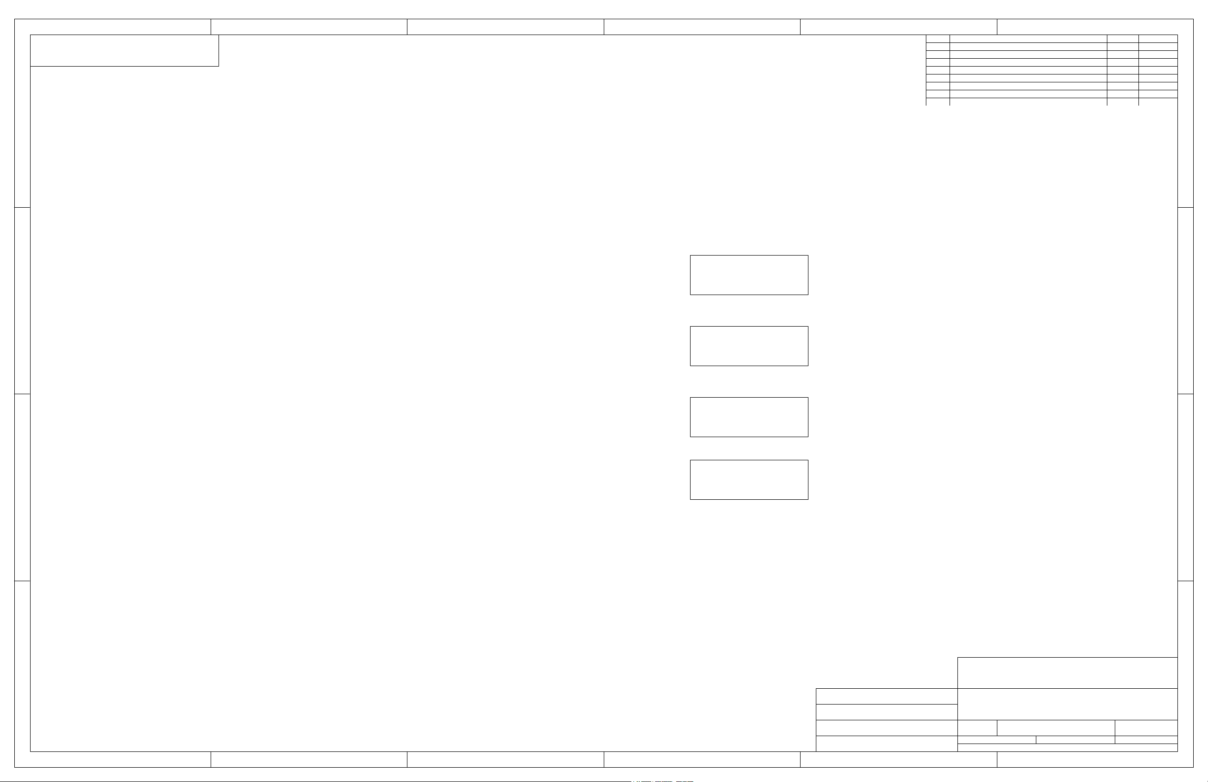
P
This document and the data disclosed herein or herewith is not
to be reproduced, used, or disclosed in whole or in part to
anyone without the written permission of THAT Corporation.
54321
A PRODUCTION RELEASE PER ECO 5344 6-28-02
6
Date ApprovedDescriptionRev
D
D
UNLESS OTHERWISE NOTED:
1.0 All resistor values are expressed in Ohms.
305-0200 305-0200.SCH
1.1 All resistors are 1/4 Watt types with their tolerance and material coded into their
value.
VALUE 1%, Metal Film 5%, Carbon Film
C
0 Ohm to 0.99 Ohms 0R to 0R976 0R to 0R91
1 Ohm to 99 Ohms 1R00 to 97R6 1R0 to 91R
100 Ohms to 999 Ohms 100R0 to 976R0 100R to 910R
1k Ohm to 9k9 Ohms 1k00 to 9k76 1k0 to 9k1
305-0300 305-0300.SCH
C
10k Ohms to 99k Ohms 10k0 to 97k6 10k to 91k
100k Ohms to 999k Ohms 100k0 to 976k0 100k to 910k
1M Ohm to 99M Ohms 1M00 to 97M6 1M0 to 91M
2. All resistor networks are 2%, 1/8 Watt types with their values expressed in Ohms.
3.0 All capacitor values are expressed in Farads
305-0400 305-0400.SCH
3.1 All 100n bypass capacitors are 20%, 50 Volt, Z5U, Ceramic Monolythic types.
3.2 All non-electrolytic capacitors are 10%, 50 Volt, X7R, Ceramic Monolythic types.
3.3 All NPO capacitors are 5%, 50 Volt, Ceramic Monolythic types.
3.4 All MY capacitors are 5%, 50 Volt, Metalized Polyester types.
3.5 All PP capacitors are 5%, 50 Volt, Metalized Polypropylene types.
3.6 All PC capacitors are 5%, 50 Volt, Metalized Polycarbonate types.
3.7 All electrolytic capacitors are 20%, 16 Volt (or higher), Aluminum Electrolyte types.
305-0500 305-0500.SCH
3.8 All TA capacitors are 20%, 16 Volt (or higher), Tantalum Electrolyte types.
B
4. For complete information on any component please see the associated bill of
materials.
B
5. All net names preceded by a / are active low signals.
45 Sumner Street
A
Checked: Date:
Proj. Eng.:
Chf. Eng.:
Production:
1 2 3 4 56
Date:
Date:
Date:
THAT Corporation
Title:
Size:
Date:
File:
QSC Digital Cinema Monitor
DCM Front Panel & Power Amp (For 1, 2 & 3)
Drawing Number:
B
28-Jun-2002 1 5
F:\DM\SH\SH000092\DEV_WORK\SH0092rA.DDB - Documents\SH0092rA.
PC-000092-00 A
A. ARANDA
Milford, MA
508-478-9200
Revision:
Sheet ofDrawn by:
A
Page 2
C
This document and the data disclosed herein or herewith is not
to be reproduced, used, or disclosed in whole or in part to
anyone without the written permission of THAT Corporation.
54321
6
Date ApprovedDescriptionRev
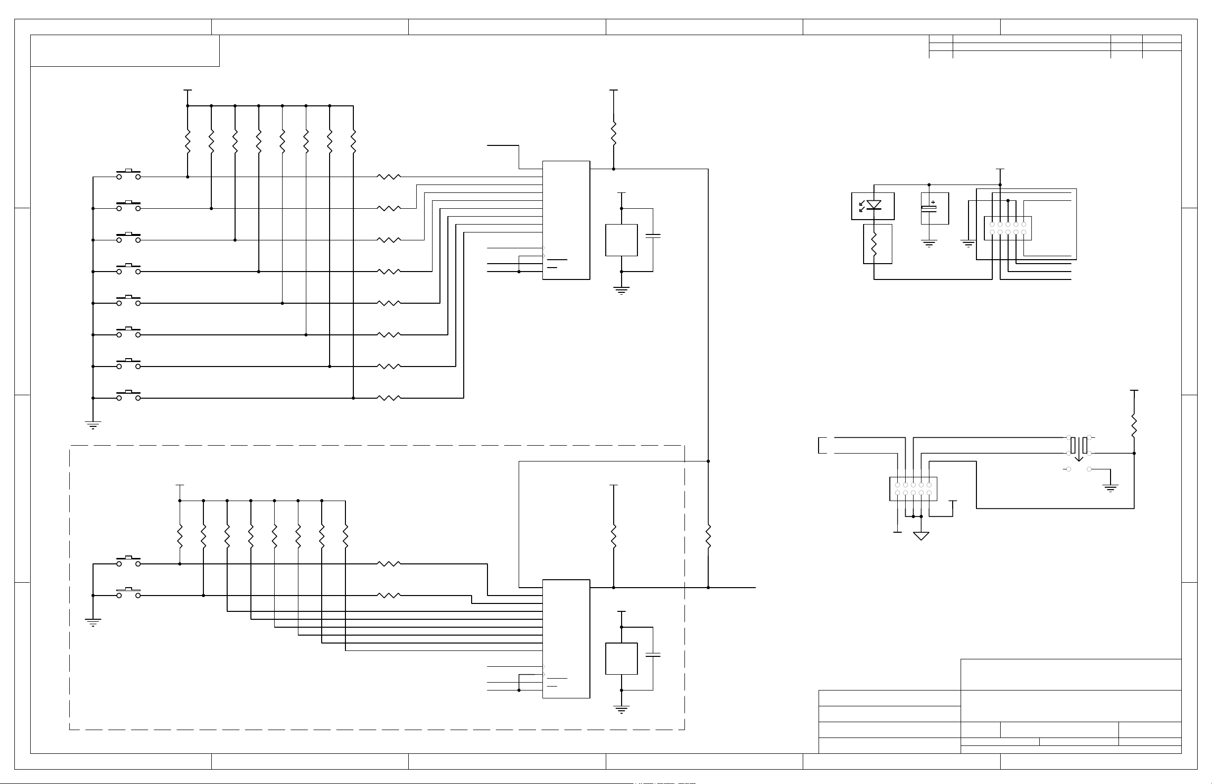
VCC
12
VCC
13
13
RN1B
10k
RN10B
10k
12
RN10A
10k
RN1A
10k
14
D
MODE
SW1 SPST NO
LEFT
SW2 SPST NO
CENT
SPST NO
SW3
RITE
SPST NO
SW4
C
SW5
SW6
SW7
SW8
B
SW9 SPST NO
SW10 SPST NO
A
SURL
SPST NO
SURR
SPST NO
SUBW
SPST NO
DIAG
SPST NO
LCNT
RCNT
Parts in dashed area are used only in the DCM-2 & 3
1 2 3 4 56
15
RN1D
10k
RN10C
10k
14
15
RN10D
10k
RN1C
10k
17
16
RN10E
10k
RN1F
10k
16
17
RN10F
10k
RN1E
10k
19
18
RN10G
10k
RN1H
10k
110
19
RN10H
10k
RN1I
10k
RN2A
470R
RN3A
470R
RN2B
470R
RN3B
470R
RN2C
470R
RN3C
470R
RN2D
470R
RN3D
470R
R38
470R
R39
470R
From LED Logic
12
12
34
34
56
56
78
78
SW8
SW9
SW10
SW11
SW12
SW13
SW14
SW15
SERLED
SW0
SW1
SW2
SW3
SW4
SW5
SW6
SW7
SCK FP
SSKEYA
SSKEYB
SCK FP
SSKEYA
SSKEYB
15
1
2
3
4
5
6
7
11
12
13
10
15
1
2
3
4
5
6
7
11
12
13
10
U1A
SDI14SDO
D0
D1
D2
D3
D4
D5
D6
D7
SCLK
RCLK
LOAD
OE
74HC589B
U7A
SDI14SDO
D0
D1
D2
D3
D4
D5
D6
D7
SCLK
RCLK
LOAD
OE
74HC589B
VCC
18
RN1G
10k
9
VCC
168
VCC
U1B
74HC589B
GND
VCC
110
RN10I
10k
9
VCC
168
VCC
U7B
74HC589B
GND
C901
100n
C15
100n
PH1
LINK
PH1 used only
in DCM-1
MISO FP
To
Compressor
D33
RED
R1
470R
From Rear Panel Bypass Mode Switch
MONOUT
MONMUTE
P2
HDR 5X2
1 2
3 4
V-
Checked: Date:
Proj. Eng.:
Chf. Eng.:
Production:
Date:
Date:
Date:
D
From Rear Panel
VCC
SSLED
C7
10u
1 2
3 4
5 6
/CLIP
STDBY
STDBYC
V+
5 6
7 8
9 10
/BYPASS
THAT Corporation
Title:
SSKEYB
P1
HDR 5X2
SSKEYA
7 8
9 10
MISO FP
SCK FP
MOSI FP
C
VCC
DPDT-S
4
5
6SW11
Normal
1
2
3
Bypass
R3
4k7
45 Sumner Street
Milford, MA
508-478-9200
B
A
DCM FRONT PANEL
I/O Interface & Button Logic
Size:
Date:
File:
Drawing Number:
B
28-Jun-2002 2 5
F:\DM\SH\SH000092\DEV_WORK\SH0092rA.DDB - Documents\305-0200.S
PC-000092-00 A
A. ARANDA
Revision:
Sheet ofDrawn by:
Page 3
C
This document and the data disclosed herein or herewith is not
to be reproduced, used, or disclosed in whole or in part to
anyone without the written permission of THAT Corporation.
54321
6
Date ApprovedDescriptionRev
D
C
B
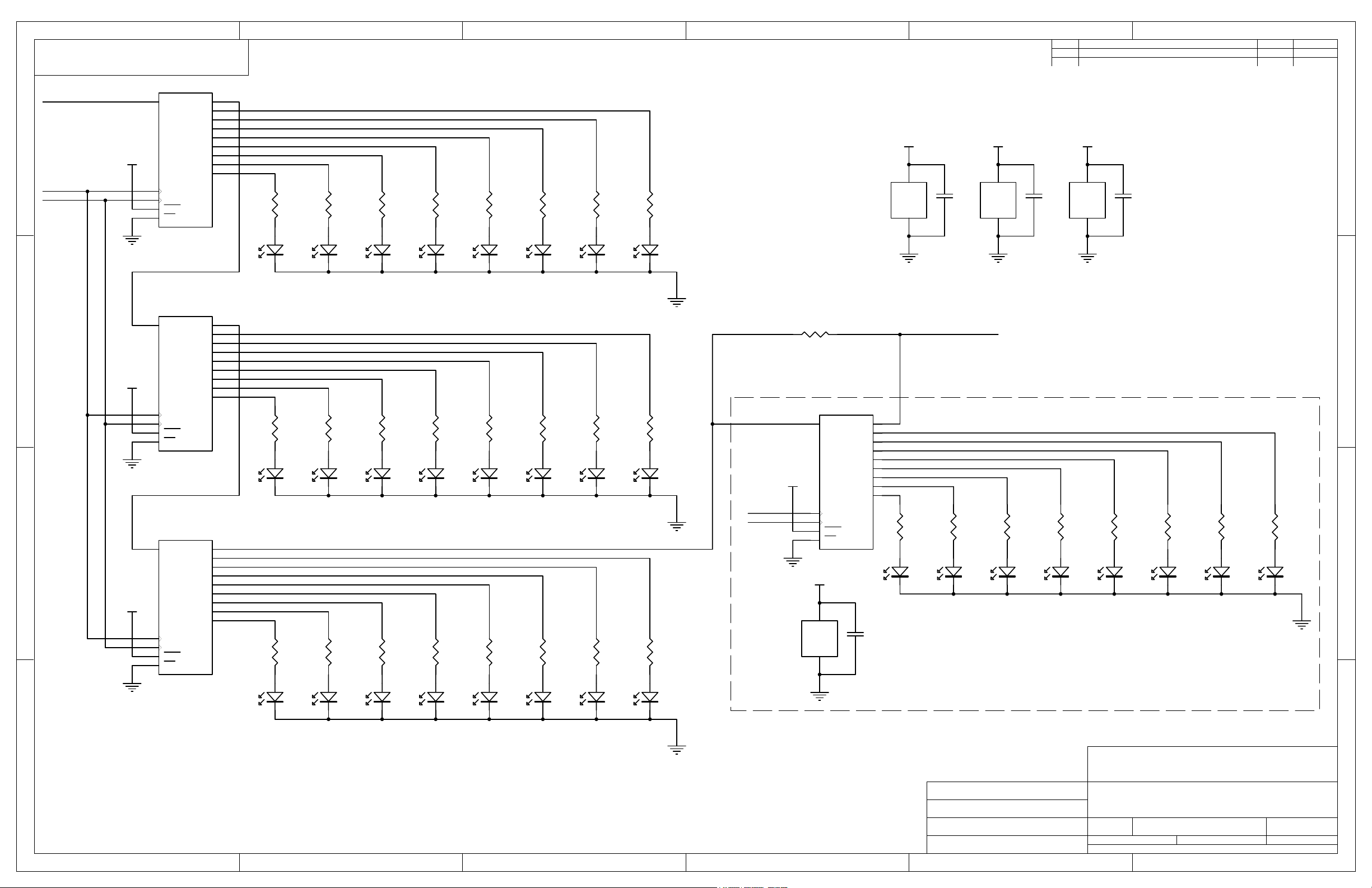
MOSI FP
SCK FP
SSLED
VCC
VCC
VCC
11
12
10
13
11
12
10
13
11
12
10
13
U2A
SDI14SDO
SCLK
RCLK
CLR
OE
74HC595B
U3A
SDI14SDO
SCLK
RCLK
CLR
OE
74HC595B
U4A
SDI14SDO
SCLK
RCLK
CLR
OE
74HC595B
Q0
Q1
Q2
Q3
Q4
Q5
Q6
Q7
Q0
Q1
Q2
Q3
Q4
Q5
Q6
Q7
Q0
Q1
Q2
Q3
Q4
Q5
Q6
Q7
9
15
1
2
3
4
5
6
7
78
RN4D
470R
D19
GRN
POWER FAULT AMP
9
15
1
2
3
4
5
6
7
RN7D
470R
7 8
D5
GRN
PROC PROC PROC
SL SR SUB
9
15
1
2
3
4
5
6
7
78
RN9D
470R
D24
YEL
RN4C
470R
5 6
RN6D
470R
7 8
RN8D
470R
7 8
D18
RED
D7
GRN
D23
YEL
L2
34
RN4B
470R
RN7C
470R
5 6
RN9C
470R
5 6
D17
YEL
D6
GRN
D22
YEL
78
RN4A
470R
1 2
D14
YEL
MODE MODE
RN6C
470R
5 6
D13
YEL
AMP AMP
L1 C1
RN8C
470R
5 6
D21
YEL
PROCAMP
RN5D
470R
RN7B
470R
3 4
RN9B
470R
3 4
D4
GRN
D12
YEL
D20
YEL
56
RN5C
470R
D3
GRN
PROC PROC PROC
LCR
RN6B
470R
3 4
D11
YEL
AMP AMP AMP
R1 SL1
RN8B
470R
3 4
D8
YEL
12
RN5A
470R
RN7A
470R
1 2
RN9A
470R
1 2
D2
GRN
D10
YEL
D16
YEL
SR1
34
RN5B
470R
RN6A
470R
1 2
RN8A
470R
1 2
D1
GRN
D9
YEL
D15
YEL
SCK FP
SSLED
PH2 used only
in DCM-1
PH2
LINK
U8A
VCC
11
12
10
13
74HC595B
VCC
168
VCC
U8B
74HC595B
GND
SDI14SDO
Q0
Q1
Q2
Q3
Q4
Q5
Q6
Q7
SCLK
RCLK
CLR
OE
VCC VCC VCC
168
VCC
U2B
74HC595B
GND
9
15
1
2
3
4
5
6
7
RN12D
470R
7 8
D28
YEL
AMP AMP AMP
C2 R2 LC2
C17
100n
C903
100n
5 6
Parts in dashed area are used only in the DCM-2 & 3
SERLED
RN12C
470R
D27
YEL
168
VCC
U3B
74HC595B
GND
To Button Logic
3 4
RN12B
470R
D26
YEL
C904
100n
1 2
AMP
RC2
VCC
U4B
74HC595B
GND
RN12A
470R
D25
YEL
168
C905
100n
56
RN11C
470R
D30
GRN
PROC PROC AMP
LC RC LC1
34
RN11B
470R
D31
GRN
RN11A
470R
1 2
D32
YEL
7 8
AMP
RC1
RN11D
470R
D29
YEL
D
C
B
AMP AMP AMP
SL2 SL3
A
1 2 3 4 56
SR2
AMP AMP
SR3 SUB1
AMP AMP AMP
SUB2 SUB3 SUB4
Checked: Date:
Proj. Eng.:
Chf. Eng.:
Production:
Date:
Date:
Date:
45 Sumner Street
THAT Corporation
Title:
DCM FRONT PANEL
Milford, MA
508-478-9200
LED Driver Logic
Size:
Date:
File:
Drawing Number:
B
28-Jun-2002 3 5
F:\DM\SH\SH000092\DEV_WORK\SH0092rA.DDB - Documents\305-0300.S
PC000092-00 A
A. ARANDA
Revision:
Sheet ofDrawn by:
A
Page 4
C
This document and the data disclosed herein or herewith is not
to be reproduced, used, or disclosed in whole or in part to
anyone without the written permission of THAT Corporation.
V+
D
C
MONOUT
Maximum
Input level
+10 dBV
B
C22
100n
MY
D34
1N4148
D35
1N4148
V-
Low Frequency Peak
R11
3k3
C19
100n
MY
R18
100k
54321
R20
51R
C24
100p NPO
C29
100p NPO
R21
51R
BUFFOUT VCAIN
6
OA2
8
U5C
4301P
J1
TP
Optional
Symmetry
Trim
Front Panel
Test points
J2
TP
C26
10u
7
0 dB-50 dB
R26
2k4
C27
10u
RMS
R13
330k
R25
10k
VOL IN1
R2
10M
4301P
CT
4
5
IN
IT
OUT
RMS
C25
10u
R24
10k
V-
Monitor
Volume
Control
1
2
R4
2M0
VR1
10k POT
U5B
VR2
50k TRIM
V-
R8
20k
C23
560p
R19
33k
High Frequency Boost
NI1
R6
330k
R5
51R
19
20
R9
3k6
V+
C11
100n
17
C9
EC
100n
Z5U
R10
10k
OA1
U5D
4301P
Compression
Ratio = 1.4 : 1
IN
18
15
16
EC+
EC-
C28
10u
14
SYM
GND
9
V+
11
10
C10
100n
V+
V-
OUT
C8
IN3
100p NPO
R7
13
20k
U5A
4301P
MONMUTE
12
R29
10k
R37
10k
OA3
V-
+7 dBV
Max Output
CMPOUT
V+
Q1
2SC1815
R23
47K
R22
100k
C18
100n
Z5U
Q2
J174
R32
10k
R36
1k0
AMPIN
6
Date ApprovedDescriptionRev
Attenuation
-20 dB
P5
1
2
3
HDR 3X1
To Power Amp
-18 dBV Max Input
D
C
B
V-
45 Sumner Street
A
Checked: Date:
Proj. Eng.:
Chf. Eng.:
Production:
1 2 3 4 56
Date:
Date:
Date:
THAT Corporation
Title:
Size:
Date:
File:
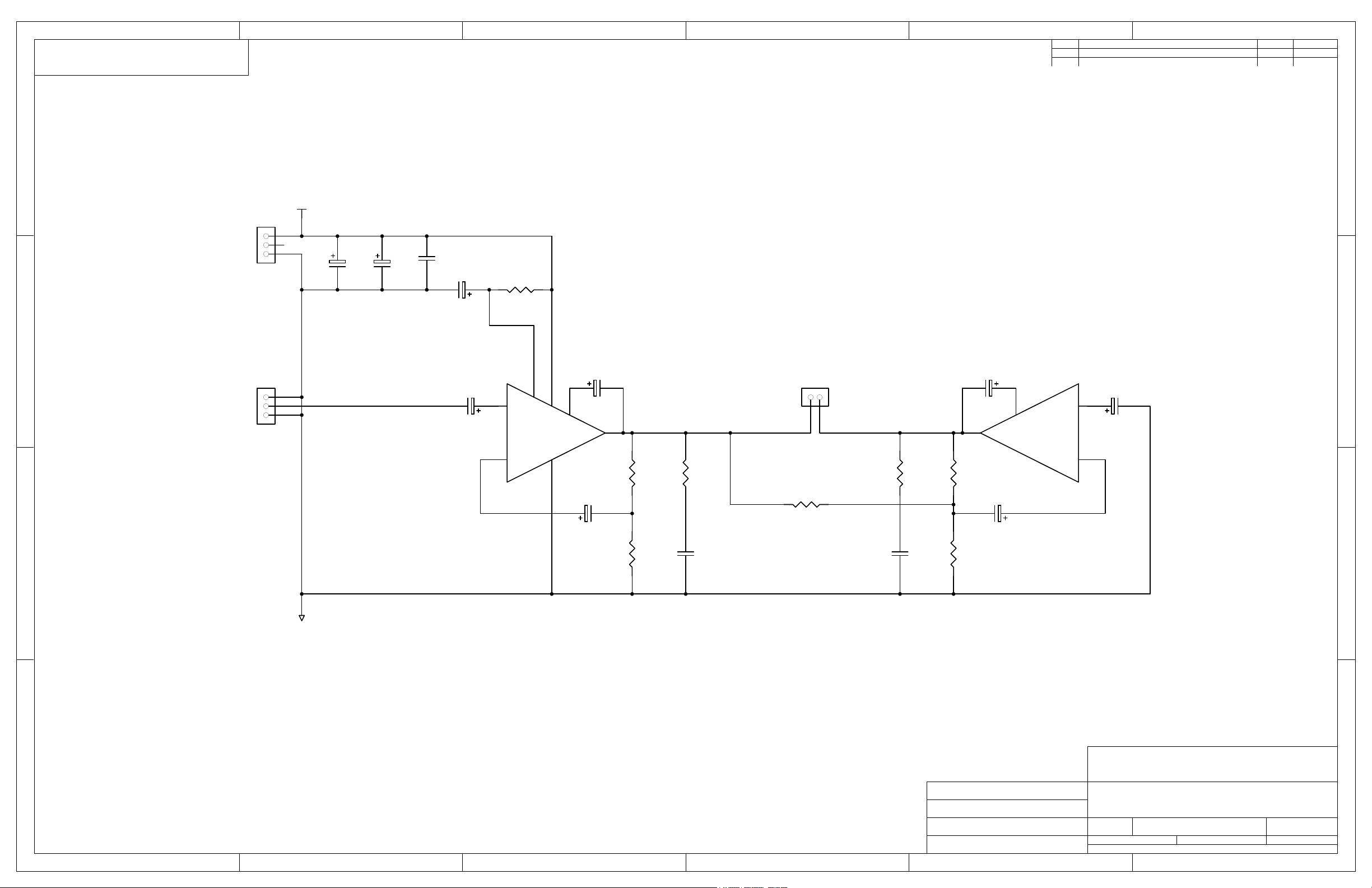
DCM FRONT PANEL
Buffer / Compressor
Drawing Number:
B
28-Jun-2002 4 5
F:\DM\SH\SH000092\DEV_WORK\SH0092rA.DDB - Documents\305-0400.S
PC-000092-00 A
A. ARANDA
Milford, MA
508-478-9200
Revision:
Sheet ofDrawn by:
A
Page 5
C
This document and the data disclosed herein or herewith is not
to be reproduced, used, or disclosed in whole or in part to
anyone without the written permission of THAT Corporation.
54321
6
Date ApprovedDescriptionRev
D
VPA+
From
Power
Supply
C
From
Front
Panel
P8
HDR 3X1
P7
HDR 3X1
3
2
1
1
2
3
C20
100u
C21
100u
PWRAMP
C14
100n
C6
10u
C12
1u
R35
120k
VCC
GND
11
BSTR
OUT
C4
100u
U6A
TDA2005M
10
R17
1k0
3
9
1
IN+
SVRR
2
IN-
6
Amp Gain = 34 dB
Maximum Power = 10.4 Watts at clipping
Maximum Input = -18 dBV (output clips)
To 4 Ohm
Speaker
1
2
R16
1R0
SPKR+
P3
HDR 2X1
SPKR-
R34
1R0
R14
1k0
8
C3
100u
U6B
TDA2005M
OUT
7
BSTR
IN+
IN-
C5
5
1u
4
D
C
C2
470u
10V
B
PAGND
A
1 2 3 4 56
R12
36R
C13
100n
Z5U
R15
1k0
C16
100n
Z5U
Checked: Date:
Proj. Eng.:
Chf. Eng.:
Production:
R33
36R
C1
470u
10V
Date:
Date:
Date:
45 Sumner Street
THAT Corporation
Title:
DCM FRONT PANEL
Milford, MA
508-478-9200
Power Amplifier Module
Size:
Date:
File:
Drawing Number:
B
28-Jun-2002 5 5
F:\DM\SH\SH000092\DEV_WORK\SH0092rA.DDB - Documents\305-0500.S
PC-000092-00 A
A. ARANDA
Revision:
Sheet ofDrawn by:
B
A
Page 6
This document and the data disclosed herein or herewith is not
to be reproduced, used, or disclosed in whole or in part to
anyone without the written permission of THAT Corporation.
54321
A PRODUCTION RELEASE PER ECO 5344 6-28-02
6
Date ApprovedDescriptionRev
D
304-0204 304-0204.SCH
304-0304 304-0304.SCH
304-1004 304-1004.SCH
304-1104 304-1104.SCH
D
UNLESS OTHERWISE NOTED:
1.0 All resistor values are expressed in Ohms.
304-0404 304-0404.SCH
304-1204 304-1204.SCH
1.1 All resistors are 1/8 Watt SMT types with their tolerance and material coded into their value.
VALUE 1%, Metal Film 5%, Carbon Film
0 Ohm to 0.99 Ohms 0R to 0R976 0R to 0R91
C
1 Ohm to 99 Ohms 1R00 to 97R6 1R0 to 91R
100 Ohms to 999 Ohms 100R0 to 976R0 100R to 910R
C
1k Ohm to 9k9 Ohms 1k00 to 9k76 1k0 to 9k1
10k Ohms to 99k Ohms 10k0 to 97k6 10k to 91k
304-0504 304-0504.SCH
304-1304 304-1304.SCH
100k Ohms to 999k Ohms 100k0 to 976k0 100k to 910k
1M Ohm to 99M Ohms 1M00 to 97M6 1M0 to 91M
2. All resistor networks are 2%, 1/8 Watt types with their values expressed in Ohms.
3.0 All capacitor values are expressed in Farads
3.1 All 100n bypass capacitors are 10%, 50 Volt, X7R, Ceramic Monolythic types.
304-0604 304-0604.SCH
304-1404 304-1404.SCH
3.2 All 100p RF capacitors are 5%, 50 Volt, NP0, Ceramic Monolythic types.
3.3 All NPO capacitors are 5%, 50 Volt, Ceramic Monolythic types.
3.4 All MY capacitors are 5%, 50 Volt, Metalized Polyester types.
3.5 All PP capacitors are 5%, 50 Volt, Metalized Polypropylene types.
3.6 All PC capacitors are 5%, 50 Volt, Metalized Polycarbonate types.
3.7 All electrolytic capacitors are 20%, 16 Volt (or higher), Aluminum Electrolyte types.
3.8 All TA capacitors are 20%, 16 Volt (or higher), Tantalum Electrolyte types.
304-0704 304-0704.SCH
304-1504 304-1504.SCH
4. For complete information on any component please see the associated bill of materials.
5. All net names preceded by a / are active low signals.
B
B
6. V+ = +12 Vdc, V- = -12 Vdc, VCC = +5 Vdc
304-0804 304-0804.SCH
304-0904 304-0904.SCH
A
1 2 3 4 56
304-1604 304-1604.SCH
304-1704 304-1704.SCH
Checked: Date:
Proj. Eng.:
Chf. Eng.:
Production:
Date:
Date:
Date:
45 Sumner Street
THAT Corporation
Title:
QSC Digital Cinema Monitor
Milford, MA
508-478-9200
DCM-1 Rear Panel PCB
Size:
Date:
File:
Drawing Number:
B
28-Jun-2002 1 17
C:\AA\PC0093rA\SH0093rA.DDB - Documents\SH0093rA.PRJ
PC-000093-00 A
A. ARANDA
Revision:
Sheet ofDrawn by:
A
Page 7
This document and the data disclosed herein or herewith is not
to be reproduced, used, or disclosed in whole or in part to
anyone without the written permission of THAT Corporation.
54321
6
Date ApprovedDescriptionRev
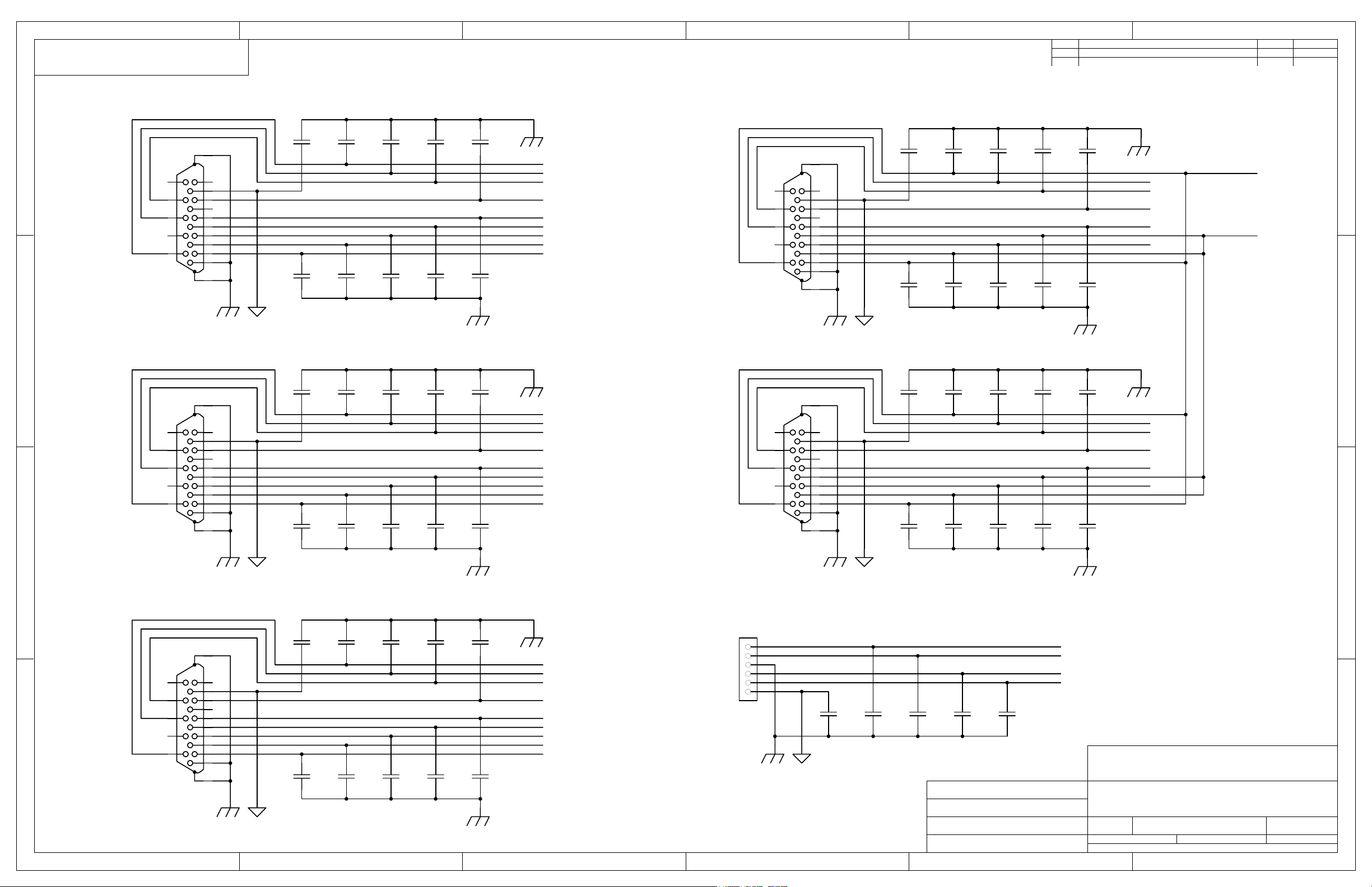
LEFT CHANNEL
D
M2
15
14
13
12
11
J1
DB15HD
C
5
10
4
9
3
8
2
7
1
6
M1
C317
100p
C1
100p
C6
100p
C2
100p
C7
100p
C3
100p
C8
100p
C4
100p
C9
100p
A2- OUT
A2 VMON
A2 IMON
A1 IMON
A1 VMON
A2+ OUT
STDa
A1+ OUT
A1- OUT
C5
100p
J7
DB15HD
CENTER CHANNEL
15
14
13
12
11
J2
DB15HD
M2
5
10
4
9
3
8
2
7
1
6
M1
C318
100p
C10
100p
C15
100p
C11
100p
C16
100p
C12
100p
C17
100p
C13
100p
C18
100p
B2- OUT
B2 VMON
B2 IMON
B1 IMON
B1 VMON
B2+ OUT
STDb
B1+ OUT
B1- OUT
C14
100p
J8
DB15HD
SUBS 1 & 2
15
14
13
12
11
SUBS 3 & 4
15
14
13
12
11
M2
5
10
4
9
3
8
2
7
1
6
M1
M2
5
10
4
9
3
8
2
7
1
6
M1
C320
100p
C209
100p
C321
100p
C28
100p
C214
100p
C210
100p
C96
100p
C39
100p
C215
100p
C211
100p
C119
100p
C91
100p
C216
100p
C212
100p
C136
100p
C92
100p
C217
100p
D2 VMON
D2 IMON
D1 IMON
D1 VMON
STDd
C213
100p
C139
100p
E2 VMON
E2 IMON
E1 IMON
E1 VMON
STDe
C95
100p
D
SW- OUT
SW+ OUT
C
B
B
RIGHT CHANNEL
C319
M2
15
14
13
12
11
A
J3
DB15HD
1 2 3 4 56
5
10
4
9
3
8
2
7
1
6
M1
100p
C19
100p
C24
100p
C20
100p
C25
100p
C21
100p
C26
100p
C22
100p
C27
100p
C23
100p
C2- OUT
C2 VMON
C2 IMON
C1 IMON
C1 VMON
C2+ OUT
STDc
C1+ OUT
C1- OUT
P1
TRM BLK
From Remote Powered
Subwoofer Output Driver
From Hard of Hearing
Output Driver
THAT Corporation
Title:
Size:
B
28-Jun-2002 3 17
Date:
C:\AA\PC0093rA\SH0093rA.DDB - Documents\304-0304.SCH
File:
DCM-1 Rear Panel PCB
Screen & Subwoofer Dataports, Aux Outputs
Drawing Number:
45 Sumner Street
Milford, MA
508-478-9200
PC-000093-00 A
A. ARANDA
Revision:
Sheet ofDrawn by:
A
C278
100p
Date:
Date:
Date:
PSW+
PSW-
HOH+
HOH-
1
2
3
4
5
6
C328
100p
C288
100p
C285
100p
Checked: Date:
Proj. Eng.:
Chf. Eng.:
Production:
C283
100p
Page 8

This document and the data disclosed herein or herewith is not
to be reproduced, used, or disclosed in whole or in part to
anyone without the written permission of THAT Corporation.
54321
6
Date ApprovedDescriptionRev
C181
PROCESSOR
INPUTS
D
C
J9
DB25S
M1
1
14
2
15
3
16
4
17
5
18
6
19
7
20
8
21
9
22
10
23
11
24
12
25
13
M2
C88
100p
C99
100p
C90
100p
C100
100p
C93
100p
C101
100p
C94
100p
C102
100p
C98
100p
C103
100p
C97
100p
LL+
CC+
RR+
SLSL+
SRSR+
SWSW+
C104
100p
Link With
Ribbon Cable
To Input
Buffer
To Input Buffer
& Passive Crossover
To Input
Buffer
123
4
P16
HDR 4X1
P17
HDR 4X1
123
4
To Processor
Monitor
To Input Buffer
To IMON Select
Mode Switch
Surround
SR12
F2 VMON
F2 IMON
F1 IMON
F1 VMON
STDf
G2 VMON
G2 IMON
G1 IMON
G1 VMON
STDg
100p
C199
100p
C183
100p
C201
100p
C182
100p
C200
100p
C179
100p
C197
100p
C323
100p
C324
100p
C178
100p
C196
100p
C322
100p
C325
100p
C177
100p
C195
100p
C175
100p
C193
100p
C176
100p
C194
100p
M2
M1
M2
M1
5
10
4
9
3
8
2
7
1
6
5
10
4
9
3
8
2
7
1
6
J4
DB15HD
J6
DB15HD
15
14
13
12
11
SURROUND
DATAPORT 1
15
14
13
12
11
SURROUND
DATPORT 2
D
C
SW1A
4PDT
B
PH5
SURROUND
INSERT
M2
5
9
4
8
3
7
2
6
1
P3
DB9P2
A
M1
1 2 3 4 56
LINK
PH4
LINK
C180
100p
C189
100p
C198
100p
C313
100p
C314
100p
C315
100p
C316
100p
SR-B
SB-R
SL-B
SB-L
SLINSLIN+
SRINSRIN+
SL12
SW1B
4PDT
SR3
SW1C
4PDT
SL3
SW1D
4PDT
H2 VMON
H2 IMON
H1 IMON
H1 VMON
STDh
C190
100p
C192
100p
Checked: Date:
Proj. Eng.:
Chf. Eng.:
Production:
C191
100p
C188
100p
Date:
Date:
Date:
C326
100p
C187
100p
C327
100p
C186
100p
C184
100p
C185
100p
THAT Corporation
Title:
DCM-1 Rear Panel PCB
M2
M1
5
10
4
9
3
8
2
7
1
6
15
14
13
12
11
SURROUND
DATAPORT 3
J5
DB15HD
45 Sumner Street
Milford, MA
508-478-9200
Surround Dataports & Insert, Processor Input
Size:
Date:
File:
Drawing Number:
B
28-Jun-2002 4 17
C:\AA\PC0093rA\SH0093rA.DDB - Documents\304-0404.SCH
PC-000093-00 A
A. ARANDA
Revision:
Sheet ofDrawn by:
B
A
Page 9

This document and the data disclosed herein or herewith is not
to be reproduced, used, or disclosed in whole or in part to
anyone without the written permission of THAT Corporation.
D
C
B
A
L-
From Left
Processor Input
L+
C-
From Center
Processor Input
C+
R-
Right
Processor Input
R+ MCLK
SW-
From Subwoofer
Processor Input
SW+
RN5B
22k
RN5C
22k
RN6B
2 7
22k
RN6C
3 6
22k
RN7B
2 7
22k
RN7C
3 6
22k
RN23B
22k
RN23C
22k
1 2 3 4 56
1 8
27
6
5
36
4 5
2
3
2
3
1 8
27
6
5
36
4 5
C37
33p NPO
RN5A
22k
RN5D
22k
C105
33p NPO
C106
33p NPO
RN6A
22k
RN6D
22k
C107
33p NPO
C108
33p NPO
RN7A
22k
RN7D
22k
C109
33p NPO
C110
33p NPO
RN23A
22k
RN23D
22k
C111
33p NPO
7
U2B
4570B
18
1
U2A
4570B
45
18
1
U3A
4570B
45
7
U3B
4570B
LIN
CIN
RIN
SWIN
To Processor
Monitor Mix
C281
10u
To Processor
Monitor Mix
C282
10u
To Processor
Monitor Mix
C287
10u
To Processor
Monitor Mix
R183
4k99
R182
20k0
-12 dB Attenuation
(4 Vrms to 1 Vrms)
R189
20k0
R198
20k0
2
3
VREF0 VREF0
R190
4k99
2
3
VREF0 VREF0
R199
4k99
2
3
VREF1 VREF1
U4A
4570B
U5A
4570B
U6A
4570B
1
1
1
2.2VDC
R184
3k32
2.2VDC
R191
3k32
R200
3k32
TP12
TP13
6
5
6
5
6
5
R185
3k32
1
VREF0
R192
3k32
R201
3k32
1
VREF1
U4B
4570B
U5B
4570B
U6B
4570B
7
7
7
C284
1u
TA
C290
1u
TA
R197
1k0
R212
1k0
R187
150R
R188
150R
R193
150R
R194
150R
R203
150R
R204
150R
VA+
VA+
LIN+
LIN-
NPO
CIN+
CIN-
RIN+
RIN-
NPO
C132
1u
TA
C131
2n2
C138
1u
TA
C137
2n2
C127
100n
NPO
NPO
C133
100n
NPO
NPO
C129
2n2
C130
2n2
C135
2n2
C289
2n2
3
17
16
15
13
14
4
3
17
16
15
13
14
4
R186
2R0
U9
VA+
AINL+
AINL-
CMOUT
AINR+
AINR-
AGND
CS5360-KS
R202
2R0
U10
VA+
AINL+
AINL-
CMOUT
AINR+
AINR-
AGND
CS5360-KS
+5VD0
VD+
MCLK
LRCLK
SCLK
SDATA
OVFL
PU
FRAME
DIF0
DIF1
HPDEF
RESET
DGND
+5VD1
VD+
MCLK
LRCLK
SCLK
SDATA
OVFL
PU
FRAME
DIF0
DIF1
HPDEF
RESET
DGND
84
V-
84
V-
84
V-
84
V-
84
V-
A. ARANDA
6
C142
100n
C141
100n
C146
100n
C145
100n
C144
100n
C143
100n
C114
100n
C113
100n
C116
100n
C115
100n
Date ApprovedDescriptionRev
45 Sumner Street
Milford, MA
508-478-9200
Revision:
Sheet ofDrawn by:
D
C
B
A
54321
V+
C286
1u
TA
6
7
12
8
9
SD0
2
11
10
20
19
1
18
5
C292
1u
TA
6
7
12
8
9
SD1
2
11
10
20
19
1
18
5
C128
100n
From System clock
R6
75R
R7
75R
R196
75R
R5
47k
C134
100n
MCLK
LRCK
SCLK
SDI0
OF0
PKUO
FRAME
/RST
From System Clock
LRCK
SCLK
R211
75R
R195
4k7
Checked: Date:
Proj. Eng.:
Chf. Eng.:
Production:
SDI1
OF1
PKUO
/RST
From uC
From Glue
To DSP
To/From Glue
From uC
From Glue
To DSP
To/From Glue
Date:
Date:
Date:
V+
U2C
4570B
V-
V+
V+
U3C
4570B
V-
V+
V+
U4C
4570B
V-
V+
V+
U5C
4570B
V-
V+
V+
U6C
4570B
V-
THAT Corporation
Title:
Size:
Date:
File:
DCM-1 Rear Panel PCB
Input Buffers & A/D Converters
Drawing Number:
B
28-Jun-2002 5 17
C:\AA\PC0093rA\SH0093rA.DDB - Documents\304-0504.SCH
PC-000093-00 A
Page 10

This document and the data disclosed herein or herewith is not
N
N
r
to be reproduced, used, or disclosed in whole or in part to
anyone without the written permission of THAT Corporation.
D
+5VD2
C208
1u
TA
C40
100n
From Sys Clock
From
Glue
From DSP
C
From Glue
B
MCLK DAC
LRCK DAC
SCLK DAC
SDAT0 DAC
/MUTE
10
16
15
11
20
19
12
ote: In order to maintain
noninverting phase
throughout the DCM-1, the
polarity is reversed for the L
C & R lopass filter inputs.
R47
2R0
U11 CS4390-KS
6
VD+
8
MCLK
7
LRCLK
9
SCLK
SDATA
1
DEM0
2
DEM1
MUTEL
MUTER
AMUTE
DIF0
DIF1
DIF2
5
DGND
VA+
AOUTL-
AOUTL+
AOUTR-
AOUTR+
AGND
54321
+12 dB (+6 dB overall)
+6 dB (0 dB overall)
Output
VA+
+6 dB gain in low pass filter
R58
13k7
C45
220p NPO
C46
220p NPO
C49
220p NPO
C50
220p NPO
U13A
4570B
U13B
4570B
1
7
LPF0
LPF1
C43
1n0
NPO
C44
1n0
NPO
C47
1n0
NPO
C48
1n0
NPO
R51
3k32
2
3
R52
3k32
R61
13k7
R63
13k7
R108
3k32
6
5
R109
3k32
R66
13k7
C218
1u
TA
3
DAC0-
17
DAC0+
18
13
DAC1-
14
DAC1+
4
C54
100n
ote: all DAC low pass filte
capacitors have 1%
tolerances.
R59
13k7
R60
13k7
R64
13k7
R65
13k7
Attenuator
R54
2k49
R53
4k99
R28
10k0
R23
20k0
R57
2k49
R56
4k99
R55
10k0
R120
20k0
0 dB (-6 dB overall)
-6 dB (-12 dB overall)
U15C
7
L5
8
L6
U15E NJU7313M2
10
L7
11
L8
U15D NJU7313M2
24
R5
23
R6
U15F NJU7313M2
21
R7
20
R8
NJU7313M2
L-COM2
L-COM3
R-COM2
R-COM3
C55
100p NPO
2
3
100p NPO
6
5
R71
10k0
R62
10k0
C53
U14A
5532B
U14B
5532B
U8A
NJU201A
1
7
2 3
1
15 14
U8B
NJU201A
16
U8C
NJU201A
10 11
9
7 6
U8D
NJU201A
8
9
ATN0
12
22
ATN1
19
V-
V-
V-
V+
D21
1N4148
V+
D23
1N4148
V+
D26
1N4148
V+
D27
1N4148
6
D22
1N4148
RN12A
1 8
51R
D24
1N4148
RN12B
2 7
51R
D25
1N4148
RN12D
4 5
51R
D28
1N4148
RN12C
3 6
51R
Date ApprovedDescriptionRev
To Left
Dataport
A1+ OUT
A1- OUT
A2+ OUT
A2- OUT
D
C
B
From Output
V+
C42
84
100n
V+
U13C
4570B
V-
C41
100n
V-
A
1 2 3 4 56
V+
84
V+
U14C
5532B
V-
V-
C51
100n
C52
100n
U8E
NJU201A
VM+
134
VDD
GND
VSS
VM-
C302
100n
5
C303
100n
Mute Driver
Checked: Date:
Proj. Eng.:
Chf. Eng.:
Production:
OUTMUTE
Date:
Date:
Date:
V-
45 Sumner Street
THAT Corporation
Title:
DCM-1 Rear Panel PCB
Milford, MA
508-478-9200
Left Channel D/A Converter
Size:
Date:
File:
Drawing Number:
B
28-Jun-2002 6 17
C:\AA\PC0093rA\SH0093rA.DDB - Documents\304-0604.SCH
PC-000093-00 A
A. ARANDA
Revision:
Sheet ofDrawn by:
A
Page 11

This document and the data disclosed herein or herewith is not
N
r
to be reproduced, used, or disclosed in whole or in part to
anyone without the written permission of THAT Corporation.
54321
6
Date ApprovedDescriptionRev
D
C
B
A
From Sys Clock
From
Glue
From DSP
From Glue
VC+
K2A
DPDTFS
K2B
DPDTFS
C71
U19A
5532B
C69
U19B
5532B
3
5
10
8
1
7
Checked: Date:
Proj. Eng.:
Chf. Eng.:
Production:
84
V+
U18C
4570B
V-
VC-
VA+
+5VD3
C219
1u
TA
MCLK DAC
LRCK DAC
SCLK DAC
SDAT1 DAC
/MUTE
C56
100n
6
8
7
9
10
1
2
16
15
11
20
19
12
5
1 2 3 4 56
R74
2R0
U16 CS4390-KS
VD+
MCLK
LRCLK
SCLK
SDATA
DEM0
DEM1
MUTEL
MUTER
AMUTE
DIF0
DIF1
DIF2
DGND
VA+
AOUTL-
AOUTL+
AOUTR-
AOUTR+
AGND
3
DAC2-
17
18
DAC2+
13
DAC3-
14
DAC3+
4
C220
1u
TA
C70
100n
R76
13k7
R77
13k7
R80
13k7
R81
13k7
R110
3k32
C59
1n0
NPO
C60
1n0
R111
NPO
3k32
R112
3k32
C63
1n0
NPO
C64
1n0
R113
NPO
3k32
ote: all DAC low pass filte
capacitors have 1%
tolerances.
R75
13k7
R78
13k7
R79
13k7
R82
13k7
C58
100n
C57
100n
2
3
220p NPO
6
5
220p NPO
C61
220p NPO
C62
C65
220p NPO
C66
U18A
4570B
U18B
4570B
U19C
5532B
1
7
V+
V-
84
LPF2
LPF3
C67
100n
C68
100n
R67
2k49
R68
4k99
R69
10k0
R122
20k0
R70
2k49
R72
4k99
R73
10k0
R123
20k0
U15A NJU7313M2
2
L1
3
L2
4
L3
5
L4
U15B NJU7313M2
29
R1
28
R2
27
R3
26
R4
From
Processor
Input
L-COM1
R-COM1
C+
C-
ATN2
6
25
ATN3
4
9
100p NPO
R98
10k0
2
3
100p NPO
R89
10k0
6
5
Thru-hole for customization
R353
1k00
1/4 W
R354
1k00
1/4 W
C247
82n
MY
R356
100R
RN17C
51R
RN17D
51R
RN17B
51R
RN17A
51R
-6 dB
-26 dB
Date:
Date:
Date:
VR2
1k Trim
36
45
27
18
C140
330n
MY
R358
100R
-6 dB
-26 dB
CLO
B1+
CHI
B2+
10
1k Hz Passive
Crossover
Network
3
5
K3A
DPDTFS
8
K3B
DPDTFS
4
9
B1+ OUT
B1- OUT
B2+ OUT
B2- OUT
VR1
1k Trim
THAT Corporation
Title:
Size:
B
28-Jun-2002 7 17
Date:
C:\AA\PC0093rA\SH0093rA.DDB - Documents\304-0704.SCH
File:
DCM-1 Rear Panel PCB
Center D/A Converter With Bypass Xover
Drawing Number:
PC-000093-00 A
A. ARANDA
To Center
Dataport
45 Sumner Street
Milford, MA
508-478-9200
Revision:
Sheet ofDrawn by:
D
C
B
A
Page 12

This document and the data disclosed herein or herewith is not
N
r
to be reproduced, used, or disclosed in whole or in part to
anyone without the written permission of THAT Corporation.
54321
6
Date ApprovedDescriptionRev
D
VA+
VD+
MCLK
LRCLK
SCLK
SDATA
DEM0
DEM1
MUTEL
MUTER
AMUTE
DIF0
DIF1
DIF2
DGND
R101
2R0
VA+
AOUTL-
AOUTL+
AOUTR-
AOUTR+
AGND
C222
1u
TA
3
DAC4-
17
DAC4+
18
DAC5-
13
DAC5+
14
4
ote: all DAC low pass filte
capacitors have 1%
tolerances.
C86
100n
V+
84
V+
U22C
4570B
V-
V-
R91
13k7
R92
13k7
R95
13k7
R96
13k7
C74
100n
C73
100n
C75
1n0
NPO
C76
1n0
NPO
C79
1n0
NPO
C80
1n0
NPO
R114
3k32
R115
3k32
R117
3k32
R118
3k32
V+
84
V+
U23C
5532B
V-
V-
R90
13k7
R93
13k7
R94
13k7
R97
13k7
C83
100n
C84
100n
2
3
220p NPO
6
5
220p NPO
C77
220p NPO
U22A
4570B
C78
C81
220p NPO
U22B
4570B
C82
U12E
NJU201A
C87
R85
2k49
R84
4k99
R83
10k0
R124
20k0
R88
2k49
R87
4k99
R86
10k0
R126
20k0
5
VM+
134
VDD
GND
VSS
LPF4
LPF5
C304
100n
C305
1
7
U24A NJU7313M2
2
L1
3
L2
4
L3
5
L4
U24B NJU7313M2
29
R1
28
R2
27
R3
26
R4
L-COM1
R-COM1
ATN4
6
ATN5
25
From Output
Mute Driver
100p NPO
2
3
100p NPO
6
5
R125
10k0
C85
R116
10k0
OUTMUTE
U23B
5532B
1
U23A
5532B
7
U12A
NJU201A
2 3
1
15 14
U12B
NJU201A
16
U12C
NJU201A
10 11
9
7 6
U12D
NJU201A
8
THAT Corporation
VM-
100n
Checked: Date:
Proj. Eng.:
Chf. Eng.:
Production:
Date:
Date:
Date:
Title:
DCM-1 Rear Panel PCB
Right Channel D/A Converter
Size:
Date:
File:
Drawing Number:
B
28-Jun-2002 8 17
C:\AA\PC0093rA\SH0093rA.DDB - Documents\304-0804.SCH
V+
D32
1N4148
RN22A
1 8
51R
D31
1N4148
V+V-
D29
1N4148
RN22B
2 7
51R
D30
1N4148
V+
V-
D33
1N4148
RN22D
4 5
51R
D35
1N4148
V+V-
D34
1N4148
RN22C
3 6
51R
D36
1N4148
V-
PC-000093-00 A
A. ARANDA
C1+ OUT
C1- OUT
To Right
Dataport
C2+ OUT
C2- OUT
45 Sumner Street
Milford, MA
508-478-9200
Revision:
Sheet ofDrawn by:
+5VD4
C221
1u
TA
C72
100n
U20 CS4390-KS
6
From Sys Clock
From
Glue
C
From DSP
From Glue
B
A
MCLK DAC
LRCK DAC
SCLK DAC
SDAT2 DAC
/MUTE
1 2 3 4 56
8
7
9
10
1
2
16
15
11
20
19
12
5
D
C
B
A
Page 13

This document and the data disclosed herein or herewith is not
to be reproduced, used, or disclosed in whole or in part to
anyone without the written permission of THAT Corporation.
From
Processor
D
C
B
A
Input Buffer
U42D NJU7313M2
22
R-COM2
U42F NJU7313M2
21
R7
20
R8
U42E NJU7313M2
10
L7
11
L8
1 2 3 4 56
SWIN
R-COM3
L-COM3
R5
R6
Q = 0.707
24
23
Q = 2.000
19
12
R100
2k00
R38
15k0
R39
3k32
V+
84
V+
U26C
LF353B
V-
V-
C238
100n
C237
100n
54321
20.0 Hz
22.1 Hz
U28D
R5
R6
U28F
R7
R8
24.5 Hz
29.5 Hz
40.0 Hz
NJU7313M2
R-COM2
NJU7313M2
R-COM3
R159
16k9
22
19
C172
470n
MY
6
5
INT1 INT2
7
U26B
LF353B
R25
16k9
R29
75k0
R26
35k7
R30
165k
U28C
7
L5
8
L6
U28E
10
L7
11
L8
NJU7313M2
L-COM2
NJU7313M2
L-COM3
R160
16k9
9
12
C168
470n
MY
2
3
U26A
LF353B
1
Frequency Control
R102
2k00
R24
16k9
R103
2k00
6
5
R104
16k9
U27B
5532B
7
SWOUT
C280
22u
R32
75k0
R33
35k7
R31
165k
24
23
21
20
Output Attenuator
C167
1n0 NPO
R40
4k99
1
U27A
5532B
OUTMUTE
U17A
NJU201A
2 3
1
U17B
NJU201A
15 14
16
U17C
NJU201A
10 11
9
U17D
NJU201A
7 6
8
Checked: Date:
Proj. Eng.:
Chf. Eng.:
Production:
Date:
Date:
Date:
V-
V-
V-
V-
D37
1N4148
D40
1N4148
D42
1N4148
D43
1N4148
V+
D38
V+
V+
V+
1N4148
D39
1N4148
D41
1N4148
D44
1N4148
RN1B
2 7
51R
RN1A
1 8
51R
RN1D
4 5
51R
RN1C
3 6
51R
THAT Corporation
Title:
Size:
B
28-Jun-2002 9 17
Date:
C:\AA\PC0093rA\SH0093rA.DDB - Documents\304-0904.SCH
File:
DCM-1 Rear Panel PCB
Subwoofer Processing
Drawing Number:
PC-000093-00 A
V+
84
V+
U27C
5532B
V-
V-
C124
100n
C123
100n
+3 dB
0 dB
-3 dB
-6 dB
-9 dB
-12 dB
-15 dB
-18 dB
U17E
NJU201A
SUBATT
R17
4k99
R35
10k0
R16
20k0
R22
40k2
VM+
134
VDD
GND
VSS
VM-
C306
100n
C307
100n
R37
3k48
R34
6k98
R36
14k0
R41
28k0
5
U28A NJU7313M2
2
L1
3
L2
4
L3
5
L4
U28B NJU7313M2
29
R1
28
R2
27
R3
26
R4
L-COM1
R-COM1
6
25
2
3
From Output
Mute Driver
6
SW+ OUT
SW- OUT
PSW+
PSW-
A. ARANDA
Date ApprovedDescriptionRev
To Subwoofer
Dataports
To Powered
Subwoofer
Output
45 Sumner Street
Milford, MA
508-478-9200
Revision:
Sheet ofDrawn by:
D
C
B
A
Page 14

This document and the data disclosed herein or herewith is not
to be reproduced, used, or disclosed in whole or in part to
anyone without the written permission of THAT Corporation.
54321
6
Date ApprovedDescriptionRev
B1 VMON
D
From Dataport
Voltage Inputs
C
B2 VMON
F1 VMON
F2 VMON
G1 VMON
G2 VMON
H1 VMON
H2 VMON
C223 1u
C224 1u
C225 1u
C226 1u
C229 1u
C230 1u
C231 1u
C232 1u
18
RN32A
100k
18
RN30A
100k
27
27
RN32B
100k
RN30B
100k
36
RN32C
100k
36
RN30C
100k
45
45
RN32D
100k
RN30D
100k
18
RN33A
100k
18
RN31A
100k
27
27
RN33B
100k
RN31B
100k
36
RN33C
100k
36
RN31C
100k
45
RN28A
1 8
1k
RN28B
2 7
1k
RN28C
3 6
1k
RN28D
4 5
1k
RN29A
1 8
1k
RN29B
2 7
1k
RN29C
3 6
1k
RN29D
4 5
1k
45
RN31D
100k
RN33D
100k
B1 MIX
B2 MIX
F1 MIX
F2 MIX
G1 MIX
G2 MIX
H1 MIX
H2 MIX
2
3
4
5
7
8
10
11
To Amplifier
Monitor Mix
U30A NJU7313M2
L1
L2
L3
L4
U30C NJU7313M2
L5
L6
U30E NJU7313M2
L7
L8
L-COM1
L-COM2
L-COM3
V+
D
6
9
12
VMON
To Monitor
Select
R146
1M5
C297
1u
R227
28k0
1
R228
549k
C299
10u
4
SYM
IN
2
R226
1k0
8
VCC VEE
RMS
GNDBIAS
3
C150
100n
56
OUT
CAP
V-
R225
1M5
V+
7
U36
2252
R224
V-
R223
2k00
Voff
C298
10u
25k5
6
5
U33B
4570B
VMONAD
7
To uC
C
0.169 VDC
TP5
1
R221
75k0
A1 MIX
A2 MIX
C1 MIX
C2 MIX
RN26A
1k
RN26B
1k
RN26C
1k
RN26D
1k
RN27A
1k
RN27B
1k
RN27C
1k
RN27D
1k
D1 MIX
D2 MIX
E1 MIX
E2 MIX
18
27
36
45
18
27
36
45
U30B NJU7313M2
29
R1
28
R2
27
R3
26
R4
U30D NJU7313M2
24
R5
23
R6
U30F NJU7313M2
21
R7
20
R8
R-COM1
R-COM2
R-COM3
25
22
19
B
A1 VMON
A2 VMON
C1 VMON
C2 VMON
D1 VMON
D2 VMON
A
E1 VMON
E2 VMON
1 2 3 4 56
C233 1u
C234 1u
C256 1u
C257 1u
C258 1u
C259 1u
C260 1u
C261 1u
Voff
+10.75
...
0.25 dB steps
-53.0 5.0
time constant = 35mS
C296
R215
1u
1k00
TA
Output (V)Input (dBV)
0.02
...
20 mV steps
Checked: Date:
Proj. Eng.:
Chf. Eng.:
Production:
Date:
Date:
Date:
45 Sumner Street
THAT Corporation
Title:
DCM-1 Rear Panel PCB
Milford, MA
508-478-9200
Amp Voltage Monitor
Size:
Date:
File:
Drawing Number:
B
28-Jun-2002 10 17
C:\AA\PC0093rA\SH0093rA.DDB - Documents\304-1004.SCH
PC-000093-00 A
A. ARANDA
Revision:
Sheet ofDrawn by:
B
A
Page 15

This document and the data disclosed herein or herewith is not
to be reproduced, used, or disclosed in whole or in part to
anyone without the written permission of THAT Corporation.
54321
6
Date ApprovedDescriptionRev
B1 IMON
D
From Dataport
Current Inputs
C
B2 IMON
F1 IMON
F2 IMON
G1 IMON
G2 IMON
H1 IMON
H2 IMON
C263 1u
C264 1u
C265 1u
C266 1u
C267 1u
C268 1u
C269 1u
C270 1u
18
45
RN40D
100k
RN38A
100k
36
27
RN38B
100k
RN40C
100k
36
27
RN40B
100k
RN38C
100k
18
45
RN38D
100k
RN40A
100k
18
45
RN41D
100k
RN39A
100k
36
27
RN39B
100k
RN41C
100k
36
27
RN41B
100k
RN39C
100k
RN34A
1 8
1k
RN34B
2 7
1k
RN34C
3 6
1k
RN34D
4 5
1k
RN35A
1 8
1k
RN35B
2 7
1k
RN35C
3 6
1k
RN35D
4 5
1k
45
RN39D
100k
18
RN41A
100k
U34A NJU7313M2
2
L1
3
L2
4
L3
5
L4
U34C NJU7313M2
7
L5
8
L6
U34E NJU7313M2
10
L7
11
L8
L-COM1
L-COM2
L-COM3
6
9
12
IMON
To Monitor
Select
R46
1M5
C262
1u
R218
28k0
1
R219
549k
IN
C295
10u
4
SYM
2
V+
R217
1k0
8
VCC VEE
RMS
GNDBIAS
3
C148
100n
56
OUT
CAP
V-
R216
1M5
7
U32
2252
D
R214
V-
R213
2k00
Voff
C294
10u
25k5
2
3
U33A
4570B
1
IMONAD
To uC
C
A1 IMON
A2 IMON
C1 IMON
C2 IMON
B
A
1 2 3 4 56
D1 IMON
D2 IMON
E1 IMON
E2 IMON
SLIN+
SRIN+
SWIN
C271 1u
C272 1u
C273 1u
C274 1u
C275 1u
C276 1u
C277 1u
C293 1u
RN36A
1k
RN36B
1k
RN36C
1k
RN36D
1k
RN37A
1k
RN37B
1k
RN37C
1k
RN37D
1k
RN11A
1 8
1k
RN11B
2 7
1k
RN11C
3 6
1k
RN11D
4 5
1k
18
27
36
45
18
27
36
45
U34B NJU7313M2
29
R1
28
R2
27
R3
26
R4
U34D NJU7313M2
24
R5
23
R6
U34F NJU7313M2
21
R7
20
R8
U24C NJU7313M2
7
L5
8
L6
U24E NJU7313M2
10
L7
11
L8
R-COM1
R-COM2
R-COM3
L-COM2
L-COM3
25
22
19
9
12
V+
C152
84
100n
V+
U33C
4570B
V-
C151
100n
V-
Checked: Date:
Proj. Eng.:
Chf. Eng.:
Production:
Date:
Date:
Date:
45 Sumner Street
THAT Corporation
Title:
DCM-1 Rear Panel PCB
Milford, MA
508-478-9200
Amp Current Monitor
Size:
Date:
File:
Drawing Number:
B
28-Jun-2002 11 17
C:\AA\PC0093rA\SH0093rA.DDB - Documents\304-1104.SCH
PC-000093-00 A
A. ARANDA
Revision:
Sheet ofDrawn by:
B
A
Page 16

This document and the data disclosed herein or herewith is not
to be reproduced, used, or disclosed in whole or in part to
anyone without the written permission of THAT Corporation.
54321
3
6
Date ApprovedDescriptionRev
G2
1
HIBUSS
G3
AD8403
17
LOBUSS
G1
AD8403
21
SRBUSS
4
U41B
AD8403
2 7
18
U41C
4 5
22
U41A
1 8
RN46B
10k
RN46D
10k
RN46A
10k
AMPSUM
C312
10u
V+ PREF
R144
75k0
R145
20k0
VCC
C38
100n
C333
10u
U41E
16
VDD
13
SDO
9
DGND
AD8403
R129
470R
D
From VMON
Inputs (Highs)
From VMON
C
B
Inputs (Lows)
From VMON
Inputs (Surrounds)
B2 MIX
A2 MIX
C2 MIX
B1 MIX
A1 MIX
C1 MIX
F1 MIX
F2 MIX
G1 MIX
G2 MIX
H1 MIX
H2 MIX
RN42A
1 8
22k
RN42B
2 7
22k
RN42C
3 6
22k
RN42D
4 5
22k
RN43A
22k
RN43B
22k
RN43C
22k
RN43D
22k
RN44A
1 8
22k
RN44B
2 7
22k
RN44C
3 6
22k
RN44D
4 5
22k
R20
22k
R19
22k
U37A
2
L1
3
L2
4
L3
5
L4
18
27
36
45
U37B
29
R1
28
R2
27
R3
26
R4
U37C
7
L5
8
L6
U37E NJU7313M2
10
L7
11
L8
U37F NJU7313M2
21
R7
20
R8
NJU7313M2
L-COM1
NJU7313M2
R-COM1
NJU7313M2
L-COM2
L-COM3
R-COM3
C147
R18
1M5
R15
1M5
R14
1M5
C329
10u
PREF
C330
10u
PREF
C331
10u
PREF
6
25
9
12
19
6
5
R130
470R
6
5
R131
470R
2
3
33p NPO
C149
33p NPO
C279
33p NPO
U40B
4570B
U39B
4570B
U39A
4570B
2
7
19
20
7
23
24
1
6
5
2
3
C202
100p NPO
R133
21k0
SDI
CLK
SHDN
RS
CS
U25B
4570B
U25A
4570B
12
14
10
15
11
D
To Monitor
Selector
7
AMPMON
+2.5 VDC
TP16
1
1
MISO AUX
MOSI AUX
SCK AUX
/MUTE
/RST
SSDPOT
To / From Glue
From uC
V+
V+
U25C
4570B
V-
V-
V+
V+
U39C
4570B
V-
V-
V+
V+
U40C
4570B
V-
V-
C334
84
100n
C335
100n
C35
84
100n
C36
100n
C204
84
100n
C205
100n
C
B
7
NJU7313M2
R-COM2
Checked: Date:
Proj. Eng.:
Chf. Eng.:
Production:
22
Date:
Date:
Date:
45 Sumner Street
THAT Corporation
Title:
DCM-1 Rear Panel PCB
Milford, MA
508-478-9200
Amp Monitor Select & Submix
Size:
Date:
File:
Drawing Number:
B
28-Jun-2002 12 17
C:\AA\PC0093rA\SH0093rA.DDB - Documents\304-1204.SCH
PC-000093-00 A
A. ARANDA
Revision:
Sheet ofDrawn by:
A
G4
U41D
AD8403
5
SWBUSS
8
RN46C
3 6
10k
R132
2
3
PREF
470R
C120
33p NPO
U40A
4570B
6
1
D1 MIX
From VMON
Inputs (Subs)
A
1 2 3 4 56
D2 MIX
E1 MIX
E2 MIX
RN45A
1k
RN45B
1k
RN45C
1k
RN45D
1k
18
27
36
45
U24D NJU7313M2
24
R5
23
R6
U24F NJU7313M2
21
R7
20
R8
R-COM2
R-COM3
22
R135
R13
1M5
21k0
19
C332
10u
U37D
24
R5
23
R6
Page 17

This document and the data disclosed herein or herewith is not
to be reproduced, used, or disclosed in whole or in part to
anyone without the written permission of THAT Corporation.
54321
6
Date ApprovedDescriptionRev
D
LIN
CIN
From
Processor
Inputs
C
RIN
SWIN
SL+
SR+
R42
4k99
R43
4k99
R44
4k99
R45
4k99
R48
4k99
R49
4k99
Processor Input Select
U42A NJU7313M2
2
L1
3
L2
4
L3
5
L4
U42C NJU7313M2
7
L5
8
L6
L-COM1
L-COM2
6
C203
100p NPO
R181
4k99
PROCSUM
9
R21
1M5
6
5
U43B
5532B
7
From Amp Submixer
From Voltage RMS
From Current RMS
PROCMON
AMPMON
VMON
IMON
Processor / Amp
Monitor Select
U42B NJU7313M2
29
R1
28
R2
27
R3
26
R4
R-COM1
25
R121
1M5
R180
49R9
MONOUT
To Front Panel
Interface
D
C
R176
4k99
R50
10k0
RN47A
1 8
B
Center -2.1 dB Attenuation
L & R -8.1 dB Attenuation
A
1 2 3 4 56
10k
RN47B
2 7
10k
RN47C
3 6
10k
RN47D
4 5
10k
Not Used
HOHSUM
100p NPO
2
3
C117
R164
3k92
U43A
5532B
B
Nominal Output
Level = -14 dBV
1
R8
49R9
R9
49R9
HOH+
HOH-
To Hearing
Impaired
Output
V+
84
V+
U43C
5532B
V-
V-
C122
100n
C121
100n
Checked: Date:
Proj. Eng.:
Chf. Eng.:
Production:
Date:
Date:
Date:
45 Sumner Street
THAT Corporation
Title:
DCM-1 Rear Panel PCB
Milford, MA
508-478-9200
Processor Monitor Select & Hearing Impaired Mixer
Size:
Date:
File:
Drawing Number:
B
28-Jun-2002 13 17
C:\AA\PC0093rA\SH0093rA.DDB - Documents\304-1304.SCH
PC-000093-00 A
A. ARANDA
Revision:
Sheet ofDrawn by:
A
Page 18

This document and the data disclosed herein or herewith is not
to be reproduced, used, or disclosed in whole or in part to
anyone without the written permission of THAT Corporation.
From Glue
D
From uC
C
B
A
MOSI AUX
SCK AUX
SSSW0
SSSW1
SSSW2
SSSW3
SSSW4
SSSW5
SSSW6
1 2 3 4 56
R151
470R
R152
470R
R153
470R
R154
470R
R155
470R
R156
470R
R157
470R
R99
4k7
17
16
14
17
16
14
17
16
14
17
16
14
17
16
14
17
16
14
17
16
14
U15G
VDD
DATA
CK
ST
NJU7313M2
U24G
VDD
DATA
CK
ST
NJU7313M2
U28G
VDD
DATA
CK
ST
NJU7313M2
U30G
VDD
DATA
CK
ST
NJU7313M2
U34G
VDD
DATA
CK
ST
NJU7313M2
U37G
VDD
DATA
CK
ST
NJU7313M2
U42G
VDD
DATA
CK
ST
NJU7313M2
VEE
VSS
VEE
VSS
VEE
VSS
VEE
VSS
VEE
VSS
VEE
VSS
VEE
VSS
54321
VC+
C34
30
1
15
30
1
15
30
1
15
30
1
15
30
1
15
30
1
15
30
1
15
VC-
V+
V-
V+
V-
V+
V-
V+
V-
V+
V-
V+
V-
100n
C33
100n
C30
100n
C29
100n
C32
100n
C31
100n
C207
100n
C206
100n
C228
100n
C227
100n
C241
100n
C240
100n
C125
100n
C126
100n
From Glue
/MUTE
R107
10k
V+
V-
V+
V-
Q1
VC+
C291
47u
C301
47u
VC-
C310
47u
C311
47u
VM+
VM+
VM-
R105
47k
1
1
1
1
D11
1N4148
D12
1N4148
D9
1N4148
D10
1N4148
2SC4116
R106
4k7
Checked: Date:
Proj. Eng.:
Chf. Eng.:
Production:
11.4VDC
TP4
TP14
-11.4VDC
+11.4VDC
TP6
TP7
-11.4VDC
0V = Unmute
5.4V = Mute
TP3
1
R140
47k
Date:
Date:
Date:
Props up
Center Channel
During Power Down
Props Up
Output Mutes
During Power Down
OUTMUTE
To Output
Mute Switches
THAT Corporation
Title:
Analog Switch Control & Supply Prop-ups
Size:
B
28-Jun-2002 14 17
Date:
C:\AA\PC0093rA\SH0093rA.DDB - Documents\304-1404.SCH
File:
DCM-1 Rear Panel PCB
Drawing Number:
PC-000093-00 A
6
A. ARANDA
Date ApprovedDescriptionRev
45 Sumner Street
Milford, MA
508-478-9200
Revision:
Sheet ofDrawn by:
D
C
B
A
Page 19

This document and the data disclosed herein or herewith is not
to be reproduced, used, or disclosed in whole or in part to
anyone without the written permission of THAT Corporation.
BDM Interface
VCC
R134
4k7
VCC
R232
4k7
MISO
MOSI
SCK
SSAUX
/RAM
/CS0
/MR
VCC
BKGD
D
R234
4k7
C
MODA
B
R233
4k7
RXD1 TXD1
PT1
/ROM
/WR
/RD
R/W
ECLK
V+
TP9
1
+1.4VDC
A
P5
1 2
3 4
5 6
HDR 3X2
VCC
P6
1
2
3
HDR 3X1
VCC
P7
1 2
3 4
5 6
HDR 3X2
VCC
P8
1 2
3 4
5 6
7 8
9 10
HDR 5X2
P9
1 2
3 4
5 6
7 8
9 10
HDR 5X2
R10
75k0
PFI
/MR
R11
10k0
Manual
Reset
1 2 3 4 56
/RESET
MODB
Digital I/O
Test Points
Reset and power fail detect
C159
100n
U45 ADM706
2
VCC
4
6
RESET
PFI
PFO
WDO
WDI
MR1GND
VMONAD
From
Level
Detectors
IMONAD
7
5
8
3
R237
4k7
R229
1k0
R220
1k0
R239
49k9
R240
75k0
D3
1N4148
D4
1N4148
D1
1N4148
D2
1N4148
V+
V-
/RESET
/PFO
VCC
VCC
VCC
D5
1N4148
VAMON
D6
1N4148
1
TP1
TP2
1
1
TP8
+2.4VDC
R238
1k07
C300
1u
TA
VCC
C163
100n
VCC
VSSA
R142
1k0
R231
4k7
VRH
PKUI
PT1
RXD
TXD
RXD1
TXD1
MISO
MOSI
SCK
SSAUX
SSCTL
SSSW6
SSCLIP
SSLED
SSKEY
/SSKEY
RTS
CTS
SSSW0
SSSW1
SSSW2
SSSW3
SSSW4
SSSW5
SPI FP
SPI AUX
BKGD
/RESET
/XIRQ
/PFO
R/W
ECLK
MODA
MODB
L2
EMI FILTER
U47 68HC812A4
43
VDDpll
95
VDDa
85
VRH
87
AN0/PAD0
88
AN1/PAD1
89
AN2/PAD2
90
AN3/PAD3
91
AN4/PAD4
92
AN5/PAD5
93
AN6/PAD6
94
AN7/PAD7
105
IOC0/PT0
106
IOC1/PT1
107
IOC2/PT2
108
IOC3/PT3
109
IOC4/PT4
110
IOC5/PT5
111
IOC6/PT6
112
IOC7/PT7
97
RXD0/PS0
98
TXD0/PS1
99
RXD1/PS2
100
TXD1/PS3
101
MISO/PS4
102
MOSI/PS5
103
SCK/PS6
104
SS/PS7
75
KWH0/PH0
76
KWH1/PH1
77
KWH2/PH2
78
KWH3/PH3
81
KWH4/PH4
82
KWH5/PH5
83
KWH6/PH6
84
KWH7/PH7
3
KWJ0/PJ0
4
KWJ1/PJ1
5
KWJ2/PJ2
6
KWJ3/PJ3
7
KWJ4/PJ4
8
KWJ5/PJ5
9
KWJ6/PJ6
10
KWJ7/PJ7
19
BKGD
40
RESET
36
XIRQ/PE0
37
IRQ/PE1
38
R/W/PE2
39
LSTRB/PE3
48
ECLK/PE4
49
MODA/PE5
50
MODB/PE6
51
ARST/PE7
44
XFC
86
VRL
96
VSSa
45
VSSpll
L1
EMI FILTER
VDD
VDD
VDD
VDD
A00/PB0
A01/PB1
A02/PB2
A03/PB3
A04/PB4
A05/PB5
A06/PB6
A07/PB7
A08/PA0
A09/PA1
A10/PA2
A11/PA3
A12/PA4
A13/PA5
A14/PA6
A15/PA7
A16/PG0
A17/PG1
A18/PG2
A19/PG3
A20/PG4
A21/PG5
D08/PC0
D09/PC1
D10/PC2
D11/PC3
D12/PC4
D13/PC5
D14/PC6
D15/PC7
D00/PD0
D01/PD1
D02/PD2
D03/PD3
D04/PD4
D05/PD5
D06/PD6
D07/PD7
CS0/PF0
CS1/PF1
CS2/PF2
CS3/PF3
CSD/PF4
CSP0/PF5
CSP1/PF6
XTAL
EXTAL
VSS
VSS
VSS
VSS
VCC
79
42
14
2
52
53
54
55
56
57
58
59
60
61
62
63
64
65
66
67
11
12
13
16
17
18
28
29
30
31
32
33
34
35
20
21
22
23
24
25
26
27
68
69
70
71
72
73
74
47
46
80
41
15
1
C153
100n
A0
A1
A2
A3
A4
A5
A6
A7
A8
A9
A10
A11
A12
A13
A14
A15
A16
D8
D9
D10
D11
D12
D13
D14
D15
SSDSP
MONMUTE
BPSTAT
DSPCTL0
DSPCTL1
SSDPOT
/RST
/CS0
/RAM
/ROM
CPUCLK
C160
100n
VCC
D7
1N4148
C161
100n
A0
A1
A2
A3
A4
A5
A6
A7
A8
A9
A10
A11
A12
A13
A14
A15
A16
/ROM
/RD
/WR
D8
1N4148
R12
1k0
Checked: Date:
Proj. Eng.:
Chf. Eng.:
Production:
C162
100n
U48A 29C257
12
A0
11
A1
10
A2
9
A3
8
A4
7
A5
6
A6
5
A7
27
A8
26
A9
23
A10
25
A11
4
A12
28
A13
29
A14
3
A15
2
A16
22
CE
24
OE
31
WE
/BYPASS
From Front Panel
Bypass Switch
54321
Date:
Date:
Date:
D0
D1
D2
D3
D4
D5
D6
D7
VCC
168
VCC
U46B
74VHC138
GND
13
14
15
17
18
19
20
21
/WR
/RD
6
U49A 61C256
9
7
/RAM
/RD
/WR
10
A0
9
A1
8
A2
7
A3
A4
6
A5
5
A6
4
A7
3
A8
25
A9
24
21
A10
23
A11
2
A12
26
A13
1
A14
20
22
27
U46A
Y0
Y1
Y2
Y3
Y4
Y5
Y6
Y7
74VHC138
C166
100n
G2A
G2B
G1
A0
A1
A2
A3
A4
A5
A6
A7
A8
A9
A10
A11
A12
A13
A14
CE
OE
WE
A
B
C
1
2
3
4
5
6
VCC
VCC
U49B
61C256
GND
14 28
D0
D1
D2
D3
D4
D5
D6
D7
D8
D9
D10
D11
D12
D13
D14
D15
C164
100n
15
14
13
12
11
10
VCC
VCC
U48B
29C256
GND
16 32
THAT Corporation
Title:
Size:
B
28-Jun-2002 15 17
Date:
C:\AA\PC0093rA\SH0093rA.DDB - Documents\304-1504.SCH
File:
DCM-1 Rear Panel PCB
Microcontroller & Peripherals
Drawing Number:
PC-000093-00 A
A. ARANDA
Date ApprovedDescriptionRev
11
D8
12
D9
13
D10
15
D11
D12
16
D13
17
D14
18
D15
19
R/W
ECLK
C165
100n
45 Sumner Street
Milford, MA
508-478-9200
Revision:
Sheet ofDrawn by:
D
C
B
A
Page 20

This document and the data disclosed herein or herewith is not
to be reproduced, used, or disclosed in whole or in part to
anyone without the written permission of THAT Corporation.
D
C
To Front
Panel Interface
To Analog Switch
& Digipot Control
ISP
Download
Port
(Cut Pin 5)
VCC
C174
100n
U50 ispLSI2032
VCC
MOSI FP
SCK FP
MOSI AUX
MISO AUX SPI FP
SCK AUX DSPCLK
1
2
3
4
5
6
7
8
VCC
P11
HDR 8X1
R260
75R
R261
75R
R245
470R
R246
470R
R243
10k0
R244
10k0
C169
100p
From uC
To/From uC
From A/D
MOSI
MISO
SCKMISO FP
SPI AUX
CPUCLK
/PFO
SSCLIP
SSCTL
/RESET
ISPSDI ISPSDO
ISPSCLK
ISPMODE
/ISPEN
FRAME
10
11
12
13
14
15
16
19
20
21
22
23
24
25
26
29
27
40
30
9
8
5
7
IO0
IO1
IO2
IO3
IO4
IO5
IO6
IO7
IO8
IO9
IO10
IO11
IO12
IO13
IO14
IO15
SDI/IN0
Y0
RESET/Y1
SCLK/Y2
GOE0
MODE
ispEN
VCC
IO16
IO17
IO18
IO19
IO20
IO21
IO22
IO23
IO24
IO25
IO26
IO27
IO28
IO29
IO30
IO31
SDO/IN1
GND
GND
6
28
OF0
31
32
OF1
33
SCLK
34
LRCK
35
36
PKUI
PKUO
37
/CLIP
38
41
42
43
DSPCK
44
1
LR DAC
2
LR DSP
3
SCK DAC
4
SCK DSP
18
17
39
C173
100n
To/From A/Ds
From uC
To Front Panel
R252
75R
R257
75R
R259
75R
R256
75R
R258
75R
LRCK DSP
SCLK DSP
LRCK DAC
SCLK DAC
TP11
1
TP10
1
To DSP
To D/As
54321
/STDBY
/MUTE
To Standby Relay Driver
To D/As & Output
Mute Driver
6
Date ApprovedDescriptionRev
D
C
C154
100n
C156
100n
C244
100p
VCC
C158
100n
C245
100p
C246
100p
C255
100p
XTXD
XCTS
XRXD
XRTS
PH3
LINK
M1
1
6
2
7
3
8
4
9
5
M2
R3
150R
J10
DB9S
VCC
147
VCC
U7G
74HCU04B
GND
C170
100n
Y1
12M288
R2
1M5
1 2
U7A
74HCU04B
C171
22p
NPO
3 4
U7B
74HCU04B
C235
22p
NPO
Checked: Date:
Proj. Eng.:
Chf. Eng.:
Production:
5 6
Date:
Date:
Date:
1213
U7F
74HCU04B
1011
U7E
74HCU04B
89
U7D
74HCU04B
Not Used
U7C
74HCU04B
R263
75R
R158
75R
R1
75R
MCLK
MCLK DAC
CPUCLK
THAT Corporation
Title:
DCM-1 Rear Panel PCB
To A/Ds
To D/As
To uC
45 Sumner Street
Milford, MA
508-478-9200
"Glue" Logic, RS-232 Driver & System Clock Oscillator
Size:
Date:
File:
Drawing Number:
B
28-Jun-2002 16 17
C:\AA\PC0093rA\SH0093rA.DDB - Documents\304-1604.SCH
PC-000093-00 A
A. ARANDA
Revision:
Sheet ofDrawn by:
B
A
U51
1
C157
100n
B
TXD
From uC
A
RTS
RXD
CTS
1 2 3 4 56
3
4
C155
100n
5
11
10
12
9
C1+
C1C2+
C2-
TD1
TD2
RD1
RD2
ADM202E
VCC
GND
RX1
RX2
V+
TX1
TX2
16
2
6
V-
15
14
7
13
8
Page 21

This document and the data disclosed herein or herewith is not
to be reproduced, used, or disclosed in whole or in part to
anyone without the written permission of THAT Corporation.
54321
6
Date ApprovedDescriptionRev
D
SCK
MISO
From uC
C
From A/D
From Glue
To D/As
From uC
B
MOSI
SSDSP
DSPCTL1
DSPCTL0
SDI0
SDI1
LRCK DSP
SCLK DSP
SDAT0 DAC
SDAT1 DAC
SDAT2 DAC
DSPCLK
/RST
DSP Development
Test Ports
P4
1 2
3 4
5 6
HDR 3X2
P15
1 2
3 4
5 6
HDR 3X2
OnCE Port
C254
100n
P10
HDR 5X2
VCC
C248
100n
12
DSI
34
DSO
56
DSCK
78
/DR
910
VCC
C249
100n
R361
10k
C250
100n
C253
22n X7R
R362
10k
R363
10k
C251
100n
26
35
41
42
43
57
56
55
51
47
46
45
50
49
27
36
37
38
39
33
32
30
31
59
58
60
61
28
17
VCC9VCC
VCC6VCC
SCK/SCL
MISO/SDA
MOSI/HA0
SS/HA2
HREQ
SDI0
SDI1
WSR
SCKR
SDO0
SDO1
SDO2
WST
SCKT
EXTAL
RESET
MODA/IRQA
MODB/IRQB
MODC/NMI
PVCC
PCAP
PINIT
PGND
DSI/OS0
DSO
DSCK/OS1
DR
1
DSP56004FJ66
MA16/MCS2/MCAS
MA17/MCS1/MRAS
GND10GND29GND
GND8GND15GND
GND
21
U21
53
48
52
VCC
MD0
MD1
MD2
MD3
MD4
MD5
MD6
MD7
MA0
MA1
MA2
MA3
MA4
MA5
MA6
MA7
MA8
MA9
MA10
MA11
MA12
MA13
MA14
MCS0
MRD
MWR
GPIO0
GPIO1
GPIO2
GPIO3
GND66GND
54
VCC40VCC
MA15/MCS3
GND34GND44GND
70
VCC
72
71
69
68
67
65
64
63
62
25
24
23
22
20
19
18
16
14
13
12
11
7
5
4
3
80
79
2
77
78
76
75
74
73
D0 DSP
D1 DSP
D2 DSP
D3 DSP
D4 DSP
D5 DSP
D6 DSP
D7 DSP
A0 DSP
A1 DSP
A2 DSP
A3 DSP
A4 DSP
A5 DSP
A6 DSP
A7 DSP
A8 DSP
A9 DSP
A10 DSP
A11 DSP
A12 DSP
A13 DSP
A14 DSP
A15 DSP
A16 DSP
/CS DSP
/RD DSP
/WR DSP
DSPCTL0
DSPTST
1
TP15
From uC
A14 DSP
A13 DSP
A12 DSP
A11 DSP
A10 DSP
A8 DSP
A6 DSP
A4 DSP
A3 DSP
A5 DSP
A9 DSP
A7 DSP
A2 DSP
A1 DSP
A0 DSP
A15 DSP
A16 DSP
U55 628128
12
A0
11
A1
10
A2
9
A3
8
A4
7
A5
6
A6
5
A7
27
A8
26
A9
23
A10
25
A11
4
A12
28
A13
3
A14
31
A15
2
A16
22
CE
24
OE
29
WE
VCC
32
16
VCC
GND
C252
100n
D0
D1
D2
D3
D4
D5
D6
D7
CE2
13
D0 DSP
14
D1 DSP
15
D2 DSP
17
D3 DSP
18
D4 DSP
19
D5 DSP
20
D6 DSP
21
D7 DSP
Delay SRAM
Also optioned for 61C256
VCC
30
D
C
B
45 Sumner Street
A
Checked: Date:
Proj. Eng.:
Chf. Eng.:
Production:
1 2 3 4 56
Date:
Date:
Date:
THAT Corporation
Title:
Size:
B
28-Jun-2002 17 17
Date:
C:\AA\PC0093rA\SH0093rA.DDB - Documents\304-1704.SCH
File:
DCM-1 Rear Panel PCB
Digital Signal Processor
Drawing Number:
PC-000093-00 A
A. ARANDA
Milford, MA
508-478-9200
Revision:
Sheet ofDrawn by:
A
 Loading...