

Page 1
CX Series
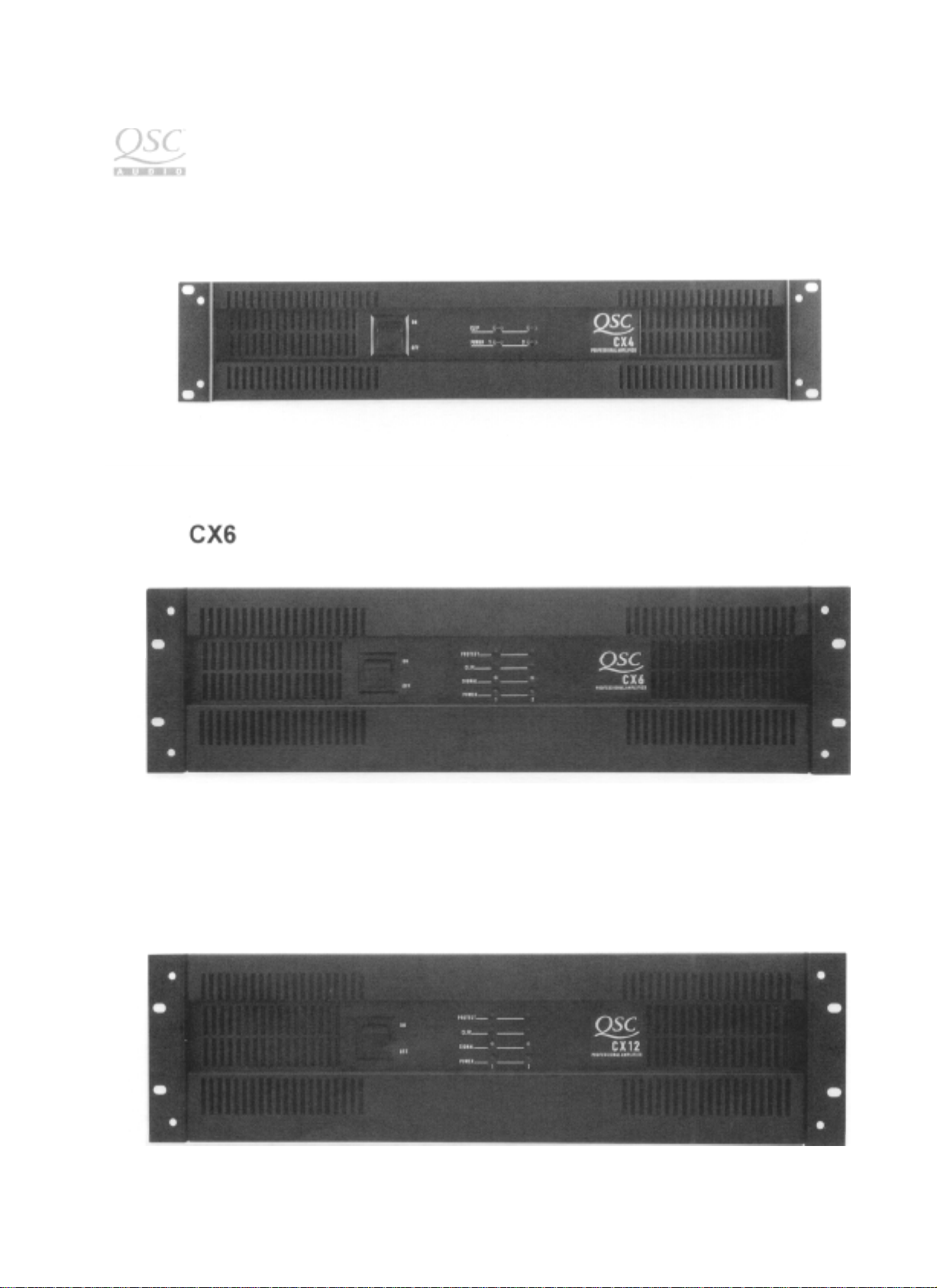
CX4
CX12
Page 2
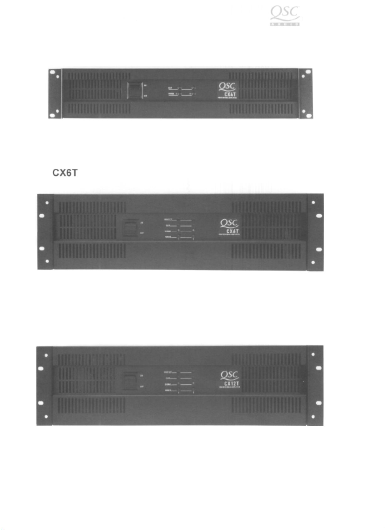
CX4T
CX Series
CX1
2T
Page 3

CX SERIES AMPLIFIER
SERVICE MANUAL
CX4 CX6 -
CX12 -
QSC Technical Services
Wats:
Local: 1-714-957-7150
Fax: 1-714-754-6173
QSC Online!
Online Computer Information System
1-800-856-6003
I-71 4-668-7567
QSC Audio Products, Inc.
1675 MacArthur Blvd.
Costa Mesa, CA 92626
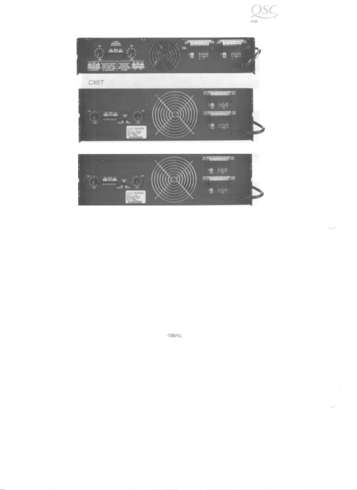
CX4T
CX6T
CX12T
1-800-772-2834
http://www.qscaudio.com
Page 4

Page 5

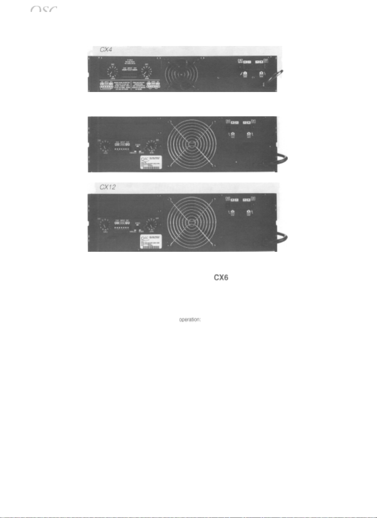
CX Series Chassis Drawings
CX4
Chassis Assembly
CX4T
Chassis Assembly
CX6 &
CX6T &
CX 4 / 4T
CX 6T &
CX4 /4T
CX6
CX12
CX12
Chassis
CX12T
Series Main Amplifier Board
/6T
Series Main Amplifier Board
/12T
Chassis
Display Board Schematic
12T
Display Board Schematic
Series Main Amplifier Board
CX Series Wiring Diagrams
CX4
Wiring Diagram
CX4
Wiring Diagram
CX4
Wiring Diagram
CX4T
Wiring Diagram
....................................................................
..................................................................
Assemblyy........................................................
Assemblyy
(120v))
(100v))
(230v))
(120v))
..............................................................
..............................................................
..............................................................
....................................................
..................................................
.............................................
.................................................
................................................
..............................................
............................................................
42
45
48
48
39
39
40
41
42
56
57
58
59
CX4T
Wiring Diagram
CX4T
Wiring Diagram
CX6 Wiring Diagram
CX6 Wiring Diagram
CX6 Wiring Diagram
CX6T
Wiring Diagram
CX6T
Wiring Diagram
CX6T
Wiring Diagram
CX12
Wiring Diagram
CX12 Wiring
CX12 Wiring Diagram
CX12T
CX12T
CX12T
Diagram
Wiring Diagram
Wiring Diagram
Wiring Diagram
(100v))
(230v))
(120v))
(100v))
(230v)
(120v))
(100v)
(230v)
(120v)
(100v))
(230v))
(120v)
(100v))
(230v))
............................................................
............................................................
..............................................................
..............................................................
..............................................................
.............................................................
.............................................................
.............................................................
.............................................................
..............................................................
.............................................................
...........................................................
...........................................................
...........................................................
60
61
62
63
64
65
66
67
68
69
70
71
72
73
Page 6
Page 7
.e
*-“-”
.a’-
-ww.,_- ~
*“arT‘
-2
CX Series
CX Series Product Specifications
CX6
cx4
Output Power (per channel):
Continuous Average Output Power both channels driven:
8
ohms,
20Hz
-
20kHz,
0.1%
THD
4
ohms,
20Hz
-
20kHz,
0.1%
THD
2
ohms,
1kHz,
1%
THD*
Continuous Average Output Power bridged mono
8 ohms,
4 ohms, 1
Voltage Gain
Sensitivity (for rated power
Distortion:
SMPTE-IM
Frequency Response:
Damping Factor
Noise:
Input Impedance
Dimensions
Faceplate
Faceplate
Chassis Depth
Weight
Shipping,
Net,
20Hz
Lbs/kg
-
20kHz,
kHz,
1% THD*
(@
direct outputs):
Width
Height
Lbs/kg
0.1% THD
@
(@
direct outputs):
8 ohms):
150
watts
225
watts
350
watts
oDeration:
450 watts
700 watts
35x (31
dB)
0.96 V rms
Less than 0.05%
20Hz
to
200
1
00dB
below rated output (20 Hz to 20
10k
unbalanced, 20k balanced
Standard
3.5” (13.3 cm)
17.9” (45.5 cm)
36/16.4
30/13.6
200
300
4500
600 watts
400 watts
40x
1
.02
20kHz, +/-0.2dB
19”
Rack Mounting
5.25” (13.3 cm)
17.9” (45.5 cm)
53/24
44/20
CX12
watts 400watts
watts
watts
(32
dB)
Vrms
650
watts
650
watts
1200 watts
1800 watts
56.5 (35
1
.00
Vrms
kHz)
5.25” (13.3 cm)
17.9” (45.5 cm)
58/26.3
50122.7
dB)
Page 8
CX4 T
CX12T
CX Series Product Specifications
CX Series
CX4T
Output Power (per channel):
Direct Output, watts per channel, both channels driven:
8 ohms, 45H.z
4 ohms,
2 ohms, 1
Isolated outputs, watts per channel, both channels driven:
70V or
70V or 100V,
25V, 45Hz-16kHz,
25V,
1
Direct Outputs, bridged mono:
8
ohms, 45
4 ohms,
Voltage Gain
Sensitivity (for rated power @ 8 ohms)
Distortion:
SMPTE-IM
Frequency Response:
Damping Factor:
Noise:
Input Impedance
Dimensions
Faceplate Width
Faceplate Height
Chassis Depth
Weight
Shipping,
Net,
Lbs/kg
-
20kHz,
0.1% THD
45Hz
-
20kHz,
0.1% THD
kHz,
1%
THD*
100V,
45Hz-16kHz,
1
kHz,
0.25% THD
kHz,
0.1% THD
Hz-20kHz,
1kHz,
1% THD
(dB):
Lbs/kg
0.25% THD
0.1% THD
0.1% THD
150 watts
225 watts
350 watts
175 watts
150 watts
450 watts
700 watts
35x (31
dB)
0.98 V rms
Less than 0.05%
-3dB @
45Hz*,
45Hz* -16kHz, +0,
*Low Frequency is limited by 18 dB/octave 45 Hz high pass filter
200 (@ direct outputs)
1
00dB
below rated output (20 Hz to 20
10k ohms unbalanced and 20k balanced
Standard
3.5” (13.3 cm)
17.9” (45.5 cm)
46/21
40/18.2
CX6T
200 watts
300 watts
450 watts
250 watts
250 watts
600 watts
900 watts
40x
1.02 Vrms
-0.2dB
@ 20kHz ; direct outputs
3dB ; isolated outputs
19”
Rack Mounting
5.25”
17.9”
62/28
55/25
(32
dB)
(13.3 cm)
(45.5 cm)
CX12T
400 watts
600 watts
900 watts
500 watts
500 watts
1200 watts
1800 watts
56.5x
(35
dB)
1 .00 Vrms
kHz)
5.25” (13.3 cm)
17.9”
(45.5 cm)
75/34
67/30.4
Page 9

CX Series
I
n t r
This manual is prepared to assist service personnel with the repair and calibration of the
CX Series power amplifiers The procedures described in this manual require advanced
technical experience and sophisticated audio test equipment.
o
d u c t i o n
A
CAUTION: To reduce the risk of electric shock, do not remove the cover. No
serviceable parts inside. Refer servicing to qualified service personnel.
WARNING: To prevent fire or electric shock, do not expose this equipment to rain
or moisture.
Documentation
This manual contains schematics, printed circuit board (PCB) drawings, parts lists, and
mechanical assembly drawings. This information should be used in conjunction with the test and
troubleshooting guide.
The electrical and electronic components are identified by circuit identification numbers on the
schematics and the parts list, The test & troubleshooting sections refer to designations shown in
the schematics.
Equivalent Parts
Although many of the electronic components used in this product may be available from
electronic suppliers, some components are specially tested and approved by
repaired with non-QSC supplied components may not meet factory specifications.
performed using non-QSC parts may void the product warranty, When in doubt, you may contact
QSC
Technical Services for assistance.
A
user-
QSC.
A product
Repairs
Parts orders to
part number (from the parts list in this manual). Parts will be shipped via UPS,
California, Shipping, handling and COD charges may be added to the cost of the parts.
Factory Repair
It may become necessary to return a product to the factory for repair. Call QSC Technical
Services for return instructions. You must obtain a Return Authorization number from QSC before
returning a product to the factory.
QSC
should include the product model number, the part description, and the QSC
F.O.B.
Costa Mesa,
QSC
Technical Services may be reached at (800) 772-2834.
3
Page 10

Test Equipment
For testing, as outlined in this manual, the following equipment will be needed.
CX Series
REQUIRED TEST EQUIPMENT
-
Distortion Analyzer capable of 0.05% THD+N
-
High Power Load Bank (8, 4, & 2 ohms) for CX
-
High Power Load Bank
-
Function Generator
-
20MHz Oscilloscope
-
Digital
Multimeter
-
Variac
(0-l 40
VAC, 20-30A)
(40,20,
& 10 ohms) for CX T
Audio Precision test and procedures files are made available, free of charge, from
Services by either sending a self addressed stamped envelope and a 3
logging on to
QSC
Online and downloading the appropriate files.
SUGGESTED TEST EQUIPMENT
*
Audio Precision System One
-
Thermocouple probe
QSC
Technical
1/2”
disk to
QSC,
or by
Test Point Schedule
The following test points are described for testing and troubleshooting references. These test
points are universal among all models. Actual voltages and current readings will vary.
AMPLIFIER SECTION
J502
Bed of Nails
Pin 1 Negative
Pin
2
Positive
Pin 3 No
Pin
Less than
Pin
Pin 6 Positive Switched Bus
Pin
Pin
Connection
4 Second Stage
1
00mVDC
5 No
Connection
Test
signal superimposed
7 No Connection.
8 Negative Switched Bus
Test
signal
(J602
is for channel 2):
15VDC IC
15VDC IC
superimposed on DC voltages.
Supply,
Supply.
OpAmp.
offset.
Rail.
on DC voltages.
Rail.
Page 11

T e s t
&
Calibration
NOTE: This test procedure will refer to the amplifier’s channels as Ch 1 (Channel
(Channel 2).
CX4 /
l SET-UP
2.
3.
4.
5.
6.
7.
l POWER UP
2.
Component designation
CX4T
1.
Connect a test load to the output terminals of the amplifier.
Make sure the Stereo / Bridge switch is set to the Stereo position.
Connect a distortion analyzer with a resolution of
terminals of the amplifier. Enable the 80kHz low pass filter.
Connect a
Set amp gain pots fully clockwise and turn on power switch.
Connect the output of the signal generator to the input terminals of the amplifier and select
an output of 0.96 (0.98 for
Plug the amplifier in to a variac and set up an AC line current monitor.
1.
Slowly raise the variac voltage and watch for excessive current draw (Line current greater
than 0.5A
European) for three seconds until the mute / protect circuit disengages. Continue to
(240V European).
Turn the power switch off and on a few times to verify the 1 - 3 second power-up muting
delay. Check both channels.
Test Procedure
dual-channel
Ch1
-
a
10X
(vertical sensitivity Ch2 - a 1X scope probe (vertical sensitivity output.
&
MUTE DELAY TEST
a.c.
at 60 Volts). This is
will
have the prefix “5” for Ch 1 and “6” for Ch2.
0.05%,
20-20kHz (or better) to the output
oscilloscope to the following test points:
CX4T) VRMS,
slightly less
2V/cm)
1 KHz sine wave.
scope probe to the channel speaker output.
0.1V/cm)
for 240V. Pause at
to the distortion analyzer
90VAC (200VAC
1)
& Ch2
120VAC
l CHANNEL OUTPUT
1.
Look for amplified signal on the scope for channel
channel 2 and repeat output test. Check for noisy
general instability on the distortion waveform while adjusting the gain control levels.
2.
Select an 8 ohm load and confirm with the gain controls that this amplifier is producing a
minimum of 170 watts at 1
channels.
l BIAS ADJUSTMENT
1. Let the amplifier cool down to room temperature.
2. With an input amplitude of
signal 20dB (80%) from full output. For the first channel to be calibrated, adjust the crossover
trimpot R512
the oscilloscope. It will be necessary to have the oscilloscope measure unfiltered distortion
for about a
kHz
just beyond the point of clipping (1 .0%
1Vrms
400mVpk-pk
1.
Switch the input signal and scope to
/
contaminated gain pots by observing
THD+N).
increase the input frequency to
crossover spike protruding from the noise trace on
15kHz.
Check both
Reduce the input
Page 12

from the amplifier in order to see the crossover spike. It is necessary to disable the 80kHz
lowpass
that
troubleshooting section of
3.
If a distortion analyzer is
filter on the analyzer for this test. Further trim
channel is at about 0.1% THD+N. If bias is
this
manual,
not
available, a less accurate crossover
not
adjustable, see the bias description and
can be made by monitoring the driver transistor (Q503 &
amplifier at room temperature, and with no input signal plugged
DC voltage across the emitter resistors of
obtain about 80mV
4.
With no signal plugged
d.c.
current from the AC service is no more than 1 .O amps
5.
Let the amplifier cool down and check / adjust channel
l SHORT CIRCUIT CURRENT
1. Select a 4 ohm load and apply a
across one of these resistors.
into the
amplifier and with an 8 ohm load, verify that the AC idle
1Vrms sinewave
0502
or Q504 (R516,
(1
kHz)
a.c.
amplifier. Ensure that power is on and that the gain controls are fully up.
2. While the amplifier is producing power into the loads, apply a short to
of each channel. In other words, apply a jumper between the red and black binding posts of
each channel. Once
should be no greater than
this
is done, the combined AC line current draw for both channels
7.5A
ac.
This is with a 120
volt
may be lower as AC line voltage is lower. As the amplifer heats up, current draw may increase
to about 9 amperes until thermal protect shutdown.
3.
While the amplifier is driving a short, observe the main supply rail voltages. Ideally, they will be
no more than 3 volts from each
4. Remove
The output should
the
short from each channel and verify that the channels recover in to 4 ohm loads.
not
experience any hang up and a full
other.
it was before a short was applied for this test.
5.
If the amplifier does
3, and 4 above pass, continue to the next
not
pass any of
the
above steps, follow the proceeding
test
FREQUENCY RESPONSE.
R512
so that the total distortion for
distortion
0504)
bias current. With the
into
R517).
and bias adjustment
the amplifier, measure the
Adjust
R512
to
2.
input signal to both channels of the
the
output binding posts
AC service to the amplifier. Current
sinewave
should be present
steps.
If steps 2,
just
as
CX Series
Setting Short Circuit Current
a.
Select a 4 ohm load and apply a
channels of the amplifier. Ensure that power is on and that the gain controls are
fully up.
b.
Turn gain controls on CH2 fully down.
4 ohm load.
c.
While
CH1
is delivering power into the load, apply a
binding posts.
d.
Observe that the
and R515 to
get
this current reading if your initial reading is off. R514 is the
positive current limit adjust and
both channels
the
adjust evenly to achieve a balanced setting.
e.
Once the correct AC current draw is
this is done,
not,
the current limits are set too low.
f,
Once the
output
the output
output
sinewave
recovers
adjust the current limit for that polarity (I + or I
same time.
Limits
1.2Vrms sinewave
CH1
A.C.
current draw is between 2.5 to 3.5 amps
R515
is the negative current limit adjust Adjust
(1
kHz)
input signal to
both
should be producing max power in the
short
across channel
A.C..
1’s
Adjust
R514
same for a change in current limiting. Both wipers need to
set,
remove the short from
the output
When
power should spring back into the 4 ohm load. If it does
into
the 4 ohm load, verify that
both
polarities of the
are clipping at the same time. If one polarity clips before the other,
-
) until
both
polarities clip at the
Page 13

g.
After the short circuit current is set and even clipping is achieved, re-apply the short
to the output to reconfirm AC line current. If the current draw is not within the
range specified, again balance the current limit
trimpots
until even clipping and the
correct AC current draw is met.
h.
Remove the input signal from CH1 and calibrate
CH2.
It is important to calibrate
only one channel at a time.
l FREQUENCY RESPONSE
CX
1. Set load to 8 ohms and scale the input generator to gain 1 watt of power from the amplifier on
each channel. Gain controls on the amplifier should be fully up.
2.
Check frequency response from
20Hz
to 20kHz (+/- 0.2dB) by sweeping random frequencies
between these extremes. This is done by verifying the same voltage amplitude at each of
the frequencies selected (within
20Hz
to 20kH.z). Check both channels,
CXT
1. Set load to 8 ohms and scale the input generator to gain 1 watt of power from the amplifier on
each channel. Gain controls on the amplifier should be fully up.
2. Check frequency response from 45Hz to
between these extremes. This is done by verifying the same voltage amplitude at each of
the frequencies selected (within 45Hz to
l POWER vs. DISTORTION TEST
CX
1. Check to ensure that both channels will produce rated power at
an 8 ohm load.
2.
While verifying rated power, check that at all frequencies the distortion measurement is less
than or equal to 0.1%. To obtain this measurement, check to ensure that the 80kHz low pass
filter is engaged on the analyzer.
CXT
1.
Check to ensure that both channels will produce rated power at
an 8 ohm load.
2.
While verifying rated power, check that at all frequencies the distortion measurement is less
than or equal to 0.1%. To obtain this measurement, check to ensure that the 80kHz low pass
filter is engaged on the analyzer. Check distributed lines
or 10 ohm loads to ensure that both channels will produce rated power at
16kHz.
16kHz (+/-
16kHz).
Check both channels.
0.2dB) by sweeping random frequencies
20Hz,
2KHz,
and
45Hz, 2KHz
(70V,
100V) with 40 ohm, 20 ohm,
and
45Hz, 2kHz,
20kHz.
16kHz.
and
into
into
l THERMAL TEST
1. Set input frequency to 1 KHz and short both channels while they are producing power into a
load.
2. AC line current draw should be about 7.0 - 8.0 amps for both channels. As the amplifier gets
hot, there will be some current drift upwards. This is not a problem as long as the case
temperature on the output transistors does not exceed 105 degrees
3.
Verify that the PTC circuit causes thermal shutdown after an extended period of time.
C.
4. While the amplifier is progressing towards thermal shutdown, look for the fan to cut in to high
speed.
5.
When thermal shutdown occurs on both channels, verify AC idle current of less than 2.5
amperes.
6.
Remove short to verify thermal protect recovery.
l OUTPUT NOISE
1. Set the amplifier gain controls all the way up, with a
1
kHz 1.00Vrms
sinewave
input signal.
Note the output level.
7
Page 14

2. Remove the input signal connector from the amplifier and measure the residual noise level
produced into the load by the amplifier. The noise signal should be 100 dB down from the
full output power point measured. A signal to noise ratio should be better than or equal to
100dB.
Check both channels.
l FINAL CHECK
This completes the amplifier test procedure for this model.Inspect the amplifier for mechanical
defects. Inspect the solder connections. Reassemble the amplifier and verify the amplifier’s
operation before returning the product to service.
CX Series
CX6 /
l SET-UP
l POWER UP
CX6T
1. Connect a test load to the output terminals of the amplifier.
2. Make sure the Stereo / Bridge switch is set to the Stereo position.
3. Connect a distortion analyzer with a resolution of
terminals of the amplifier. Enable the 80kHz low pass filter.
4. Connect a dualchannel oscilloscope to the following test points:
5.
Set amp gain pots fully clockwise and turn on power switch.
6.
Connect the output of the signal generator to the input terminals of the amplifier and select
an output of 1.15
7. Plug the amplifier in to a variac and set up an AC line current monitor.
1.
Slowly raise the variac voltage and watch for excessive current draw (Line current greater
than 0.5A
European) for three seconds until the mute
(240V European).
2.
Turn the power switch off and on a few times to verify the 1 - 3 second power-up muting
delay. Check both channels.
Test Procedure
Ch1
-
a
10X
(vertical sensitivity Ch2 - a 1X scope probe (vertical sensitivity output.
VRMS,
1 KHz sine wave.
&
MUTE DELAY TEST
a.c.
at 60 Volts). This is slightly
2V/cm)
scope probe to the channel speaker output.
less
for
/
protect circuit disengages, Continue to
0.05%,
0.1V/cm)
240V.
20-20kHz (or better) to the output
to the distortion analyzer
Pause at
90VAC (200VAC
120VAC
l CHANNEL OUTPUT
1. Look for amplified signal on the scope for channel 1.
channel 2 and repeat output test. Check for noisy
general instability on the distortion waveform while adjusting the gain control levels,
2. Select an 8 ohm load and confirm with the gain controls that this amplifier is producing a
minimum of 220 watts at 1
channels.
l BRIDGE MODE
1.
Turn the power switch off and the gain controls down.
2.
Move the bridge switch on the amp from the Stereo to Bridge position.
3. Set an 8 ohm load to both red output binding posts
4.
Apply a
0.1% THD+N and verify that the output does not collapse. The position of
does not affect the output level.
1VRMS,
1
kHz sinewave
kHz
just beyond the point of clipping (1.0%
input to channel 1 of the amplifier. Check for 600 watts at
Switch the input signal and scope to
.
/
contaminated gain pots by looking for
THD+N).
(CH1
positive and CH2 negative).
CH2’s
Check both
gain control
Page 15

CX Series
5
Turn power off and place the amplifier under test back into the Stereo mode with output loads
connected to each channel. Reinsert CH2 input plug and turn both gain controls fully up.
l BIAS ADJUSTMENT
1. Let the amplifier cool down to room temperature,
2. With an input amplitude of
signal 20dB (80%) from full output. At this point, a couple of watts of output power should be
observed at the output.
VR501 for about a
400mVpk-pk
oscilloscope. It will be necessary to have the oscilloscope measure unfiltered distortion from
the amplifier in order to see the crossover spike.It is necessary to disable the 80kHz
filter on the analyzer for this test.
channel is at about 0.1% THD+N. If bias is not settable, see the bias description and
troubleshooting section of this manual.
3.
If a distortion analyzer is not available, a less accurate crossover distortion and bias adjustment
can be made by monitoring the driver transistor
amplifier at room temperature, and with no input signal plugged into the amplifier, measure the
DC voltage across the emitter resistors of
obtain about 80mV
d.c.
4. With no signal plugged into the amplifier and with an 8 ohm load, verify that the AC idle
current from the AC service is no more than 1 .O amps
5.
Let the amplifier cool down and check/adjust channel 2.
1Vrms,
increase the input frequency to 20kHz. Reduce the input
For the first channel to be calibrated, adjust the crossover
crossover spike protruding from the noise trace on the
Further trim
VR501
(Q501 & Q502)
Q501
and
so that the total distortion for that
bias current. With the
Q502
(R501,
R502).
across one of these resistors.
a.c.
Adjust
trimpot
lowpass
VR501
to
l SHORT CIRCUIT CURRENT
1.
Select a 4 ohm load and apply a
1Vrms sinewave
(1
kHz)
input signal to both channels of the
amplifier. Ensure that power is on and that the gain controls are fully up.
2. While the amplifier is producing power into the loads, apply a short to the output binding posts
of each channel. In other words, apply a jumper between the red and black binding posts of
each channel. Once this is done, the combined AC line current draw for both channels
should be no greater than
8.0A ac.
This is with a
120VAC
service. Current may be lower as
AC line voltage is lower. As the amplifier heats up, current draw may increase to about 9A until
thermal protect shutdown.
3.
While the amplifier is driving a short, observe the main supply rail voltages. Ideally, they will be
no more than 3 volts from each other.
4. Remove the short from each channel and verify that the channels recover in to 4 ohm loads,
The output should not experience any hang up and a full
sinewave
should be present just as
it was before a short was applied for this test.
5. If the amplifier does not pass any of the above steps, follow the proceeding steps.
3, and 4 above pass, continue to the next test “Frequency Response.
”
Setting Short Circuit Current Limits
a. Select a 4 ohm load and apply a 1
.2Vrms sinewave
(1
kHz)
input signal to both
channels of the amplifier. Ensure that power is on and that the gain controls are
fully up.
b.
Turn gain controls on CH2 fully down.
CH1
should be producing max power in the
4 ohm load.
c. While
CH1
is delivering power into the load, apply a short across channel 1’s
binding posts.
d. Observe that the
VR503 to get this current reading if your initial reading is off.
A.C.
current draw is 3.0 - 4.0 amps
A.C..
Adjust
VR503
VR502
is the positive
current limit adjust and VR502 is the negative current limit adjust. Adjust both
channels the same for a change in current limiting. Both wipers need to adjust
evenly to achieve a balanced setting.
If steps 2,
and
9
Page 16

e.
Once the correct AC current draw is set, remove the short on the output, When this
is done, the output power should spring back into the 4 ohm load. If it does not,
the current limits are set too low.
f. Once the output recovers into the 4 ohm load, verify that both polarities of the
output
sinewave
adjust the current limit for that polarity (1
same time.
g.
After the short circuit current is set and even clipping is achieved,
to the output to reconfirm AC line current. If the current draw is not within the
range specified, again balance the current limit
correct AC current draw is met.
h. Remove the input signal from
only one channel at a time.
l FREQUENCY RESPONSE
1.
Set load to 8 ohms and scale the input generator to gain 1 watt of power from the amplifier on
each channel. Gain controls on the amplifier should be fully up.
2. Check frequency response from 20Hz to
between these extremes, This is done by verifying the same voltage amplitude at each of
the frequencies selected (within
outputs is between 45Hz and
CX Series
are clipping at the same time. If one polarity clips before the other,
+
or I
-
) until both polarities clip at the
trimpots
CH1
and calibrate
20kHz
(+/- 0.2dB)
20Hz
to 20kHz). The frequency extremes for the
16kHz (-3dB @
45Hz,
-0.2dB @ 20
by sweeping random frequencies
until even clipping and the
CH2.
It is important to calibrate
kHz).
re-apply
Check both channels.
the short
CX6Tdirect
l POWER vs. DISTORTION TEST
1.
Check to ensure that both channels will produce rated power at
an 8 ohm load. For the
20kHz (-3dB @
2.
While verifying rated power, check that at all frequencies the distortion measurement is less
45Hz,
CX6T
under test, check power levels between
-0.2dB @ 16
kHz).
20Hz,
2KHz,
and 20kHz. into
200Hz,
than or equal to 0.1%. To obtain this measurement, check to ensure that the 80kHz low pass
filter is engaged on the analyzer. Check distributed lines
or 10 ohm loads to ensure that both channels will produce rated power at
(70V,
100V) with 40 ohm, 20 ohm,
45Hz,
16kHz.
l THERMAL TEST
1. Set input frequency to
1
KHz and short both channels while they are producing power into a
load.
2. AC line current draw should be about 7.0 - 8.0 amps for both channels. As the amplifier gets
hot, there will be some current drift upwards. This is not a problem as long as the case
temperature on the output transistors does not exceed
105
degrees
C.
3. Verify that the PTC circuit causes thermal shutdown after an extended period of time.
4. While the amplifier is progressing towards thermal shutdown, look for the fan to cut in to high
speed.
5. When thermal shutdown occurs on both channels, verify AC idle current of less than 2.5
amperes.
6.
Remove short to verify thermal protect recovery.
l OUTPUT NOISE
1.
Set the amplifier gain controls all the way up, with a 1
kHz
1
.00Vrms
sinewave
input signal.
Note the output level.
2. Remove the input signal connector from the amplifier and measure the residual noise level
produced into the load by the amplifier. The noise signal should be 100 dB down from the
full output power point measured. A signal to noise ratio should be better than or equal to
1OOdB.
Check both channels.
2kHz,
2kHz,
and
and
Page 17

CX Series
l FINAL CHECK
This completes the amplifier test procedure for this model.Inspect the amplifier for mechanical
defects. Inspect the solder connections. Reassemble the amplifier and verify the amplifier’s
operation before returning the product to service.
CX12
l SET-UP
l POWER UP
/
CX12T
1.
Connect a test load to the output terminals of the amplifier.
2.
Make sure the Stereo / Bridge switch is set to the Stereo position.
3.
Connect a distortion analyzer with a resolution of
terminals of the amplifier. Enable the
4.
Connect a dualchannel oscilloscope to the following test points:
Set amp gain pots fully clockwise and turn on power switch.
5.
Connect the output of the signal generator to the input terminals of the amplifier and select
6.
an output of 1 .00
7.
Plug the amplifier in to a variac and set up an AC line current monitor.
&
1.
Slowly raise the variac voltage and watch for excessive current draw (Line current greater
than 0.5A a.c. at 60 Volts).
European) for three seconds until the mute / protect circuit disengages, Continue to
(240V European).
2. Turn the power switch off and on a few times to verify the 1
delay. Check both channels.
Test Procedure
80kHz
low pass filter.
Ch1
-
a 1 OX (vertical sensitivity -
Ch2 - a 1 X scope probe (vertical sensitivity - 0.
output.
VRMS,
1 KHz sine wave.
MUTE DELAY TEST
This
is slightly
2V/cm)
less
0.05%, 20-20kHz
scope probe to the channel speaker output.
1V/cm)
for 240V Pause at
(or better) to the output
to the distortion analyzer
90VAC (200VAC
-
3 second power-up muting
120VAC
l CHANNEL OUTPUT
1. Look for amplified signal on the scope for channel
channel 2 and repeat output test. Check for noisy / contaminated gain pots by looking for
general instability on the distortion waveform while adjusting the gain control levels.
2.
Select an 8 ohm load and confirm with the gain controls that this amplifier is producing a
minimum of 430 watts at 1
channels.
l BRIDGE MODE
1. Turn the power switch off and the gain controls down.
2,
Move the bridge switch on the amp from the Stereo to Bridge position.
3.
Set an 8 ohm load to both red output binding posts
the input connector from channel 2.
4. Apply a
0.1% THD+N and verify that the output does not collapse. The position of
does not affect the output level.
5,
Turn power off and place the amplifier under test back into the Stereo mode with output loads
connected to each channel. Reinsert CH2 input plug and turn both gain controls fully up.
1VRMS,
1
kHz sinewave
kHz
just beyond the point of clipping (1 .0% THD+N). Check both
input to channel 1 of the amplifier. Check for 1200 watts at
Switch the input signal and scope to
1.
(CH1
positive and CH2 negative). Remove
CH2’s
gain control
11
Page 18

l BIAS ADJUSTMENT
1. Let the amplifier cool down to room temperature.
2. With an input amplitude of
1Vrms,
increase the input frequency to 20kHz. Reduce the input
signal 20dB (80%) from full output. At this point, a couple of watts of output power should be
observed at the output.For the first channel to be calibrated, adjust the crossover
VR501
for about a
4OOmVpk-pk
crossover spike protruding from the noise trace on the
oscilloscope. It will be necessary to have the oscilloscope measure unfiltered distortion from
the amplifier in order to see the crossover spike.It is necessary to disable the 80kHz
filter on the analyzer for this test. Further trim
VR501
so that the total distortion for that
channel is at about 0.1% THD+N. If bias is not settable, see the bias description and
troubleshooting section of this manual.
3. If a distortion analyzer is not available, a less accurate crossover distortion and bias adjustment
can be made by monitoring the driver transistor
(Q501 & Q502)
bias current. With the
amplifier at room temperature, and with no input signal plugged into the amplifier, measure the
DC voltage across the emitter resistors of
obtain about 80mV
d.c.
across one of these resistors.
Q501
and
Q502 (R501, R502).
Adjust
4. With no signal plugged into the amplifier and with an 8 ohm load, verify that the AC idle
current from the AC service is no more than 1 .O amps
5.
Let the amplifier cool down and check/adjust channel
a.c.
2.
trimpot
lowpass
VR501
CX Series
to
l SHORT CIRCUIT CURRENT
1.
Select a 4 ohm load and apply a 1 Vrms
sinewave
(1
kHz)
input signal to both channels of the
amplifier. Ensure that power is on and that the gain controls are fully up.
2. While the amplifier is producing power into the loads, apply a short to the output binding posts
of each channel. In other words, apply a jumper between the red and black binding posts of
each channel. Once this is done, the combined AC line current draw for both channels
should be no greater than
8.0A
ac. This is with a
120VAC
service. Current may be lower as
AC line voltage is lower. As the amplifier heats up, current draw may increase to about 9A until
thermal protect shutdown.
3.
While the amplifier is driving a short, observe the main supply rail voltages. Ideally, they will be
no more than 3 volts from each other.
4. Remove the short from each channel and verify that the channels recover in to 4 ohm loads.
The output should not experience any hang up and a full
sinewave
should be present just as
it was before a short was applied for this test.
5. If the amplifier does not pass any of the above steps, follow the proceeding steps. If steps 2,
3, and 4 above pass, continue to the next test “Frequency Response.
”
Setting Short Circuit Current Limits
a,
Select a 4 ohm load and apply a
channels of the amplifier. Ensure that power is on and that the gain controls are
fully up.
b.
Turn gain controls on CH2 fully down.
4 ohm load.
c.
While
CH1
is delivering power into the load, apply a short across channel l’s
binding posts.
d.
Observe that the
VR503 to get this current reading if your initial reading is off.
current limit adjust and
A.C.
current draw is 5.0 - 6.0 amps
VR502
1.2Vrms sinewave
CH1
should be producing max power in the
(1
kHz)
input signal to both
A.C..
Adjust
VR502
VR503
is the positive
is the negative current limit adjust. Adjust both
and
12
Page 19

channels the same for a change in current limiting. Both wipers need to adjust
evenly to achieve a balanced setting.
e. Once the correct AC current draw is set, remove the short on the output. When this
is done, the output power should spring back into the 4 ohm load. If it does not,
the current limits are set too low.
f.
Once the output recovers into the 4 ohm load, verify that both polarities of the
output
sinewave
adjust the current limit for that polarity (1
same time.
g.
After the short circuit current is set and even clipping is achieved, reapply the short
to the output to reconfirm AC line current.If the current draw is not within the
range specified, again balance the current limit
correct AC current draw is met.
h.
Remove the input signal from
only one channel at a time.
l FREQUENCY RESPONSE
1.
Set load to 8 ohms and scale the input generator to gain 1 watt of power from the amplifier on
each channel. Gain controls on the amplifier should be fully up.
2. Check frequency response from
between these extremes. This is done by verifying the same voltage amplitude at each of
the frequencies selected (within
outputs is between
are clipping at the same time.If one polarity clips before the other,
+
or I
-
) until both polarities clip at the
45Hz
and
200Hz
200Hz
16kHz
trimpots
CH1
and calibrate
to 20kHz
(+/-
0.2dB) by sweeping random frequencies
to 20kHz). The frequency extremes for the
(-3dB @
45Hz,
-0.2dB @ 20
until even clipping and the
CH2.
It is important to calibrate
kHz).
Check both channels.
CX6Tdirect
l POWER vs. DISTORTION TEST
1.
Check to ensure that both channels will produce rated power at
an 8 ohm load. For the CX6T under test, check power levels between
20kHz
2,
While verifying rated power, check that at all frequencies the distortion measurement is less
(-3dB @ 45Hz,
-0.2dB @ 16
kHz).
200Hz,
2KHz,
200Hz,
than or equal to 0.1%. To obtain this measurement, check to ensure that the 80kHz low pass
filter is engaged on the analyzer. Check distributed lines
or 10 ohm loads to ensure that both channels will produce rated power at
(70V, 100V)
with 40 ohm, 20 ohm,
45Hz, 2kHz,
16kHz.
l THERMAL TEST
1.
Set input frequency to 1 KHz and short both channels while they are producing power into a
load.
2. AC line current draw should be about 7.0 - 8.0 amps for both channels. As the amplifier gets
hot, there will be some current drift upwards. This is not a problem as long as the case
temperature on the output transistors does not exceed 105 degrees
C.
3. Verify that the PTC circuit causes thermal shutdown after an extended period of time.
4. While the amplifier is progressing towards thermal shutdown, look for the fan to cut into high
speed.
5.
When thermal shutdown occurs on both channels, verify AC idle current of less than
amperes.
6. Remove short to verify thermal protect
recovev.
and
2kHz,
20kHz.
and
and
2.5
into
13
Page 20

l OUTPUT NOISE
1.
Set the amplifier gain controls all the way up, with a 1
kHz
1
.00Vrms
sinewave
input signal,
Note the output level.
2. Remove the input signal connector from the amplifier and measure the residual noise level
produced into the load by the amplifier. The noise signal should be 100 dB down from the
full output power point measured. A signal to noise ratio should be better than or equal to
1
00dB.
Check both channels.
l FINAL CHECK
This completes the amplifier test procedure for this model.Inspect the amplifier for mechanical
defects. Inspect the solder connections. Reassemble the amplifier and verify the amplifier’s
operation before returning the product to service.
CX Series
Page 21

.s ,.
.
CX Series
Troubleshooting
Current Draw
(Circuit breakers and fuses blow.Burning smell or smoke)
Symptoms:
-
Excessive current without signal present
l- Fast current draw
-
Medium current draw
. Slow current draw
-
Runaway current draw
Possible Causes:
-EXCESSIVE CURRENT WITHOUT SIGNAL PRESENT (Above 2A and less than 4A)
1.
The amplifier draws high current when the AC supply voltage is first applied. This symptom
may mean that there is a short in the power stages of the circuit.
2.
This could also be a misadjusted bias setting. See calibration procedures in this manual for
setting bias, Check for VR511,
diodes
D505, D506, D605,
D606
VR61
(CX6/T,
1
(CX6/T,
CX1
CX12/T),
R512, VR612 (CX4/T)
2/T), D504, D505, D604,
D605
or open
(CX4/T).
l
FAST CURRENT DRAW (increases rapidly at only a few volts AC):
1.
Reversed or shorted main bridge rectifier
BR601, BR602
(CX12/T).
Check the bridge rectifier by setting DMV to diode mode. To verify
a good bridge rectifier, connect the negative lead to
0.4 to
0.6v
at both AC terminals. Connect positive lead to
BR501, BR601 (CX4/T, CX6/T), BR501, BR502,
BR+
(BR = bridge rectifier) and check for
BR-
and check for 0.4 to
0.6v
at
both AC terminal.
2. Both supply clamping diodes shorted or reversed
D510, D512
3. Shorted or reversed C509, C510, C511,
C512, C611,
l
MEDIUM CURRENT DRAW (increases slowly, can go to 30 VAC before current becomes excessive.):
1.
Single polarity driver or output short.
2.
Open or missing bias diodes
l
SLOW CURRENT DRAW (above 60 volts AC before current begins to increase, amp may pass signal):
1.
Severely misadjusted bias circuit or defective
(CX4/T).
C612
(CX6/T),
C511,
D505,
C512, C609, C610, C611,
C512, C513, C514, C611, C612,
D506
(CX6/T,
D512, D513, D612,
CX12/T),
D504,
D505-506 (CX6/T,
D613
C612
C613,
D505
CX12/T),
(CX6/T,
CX12/T),
(CX12/T),C511,
C614 (CX4/T).
(CX4/T).
R512, R612, D504,
D505 (CX4/T).
2.
Severe oscillation causing current drain. Check all feedback components and high frequency
snubber circuit
l RUNAWAY CURRENT DRAW
1.
A reversed filter capacitor: caution, may vent explosively.
(30-40V
AC before current begins to increase or runaway):
15
Page 22

Protection, Standby, and Power Up.
(The amplifier locks up or does not startup and shut off correctly)
CX Series
Model
CX4/4
T
Symptoms:
l Amplifier does not come out of protect
-
Model
Amplifier
-
Muting delay
-
Pilot LED not working
-
Fan doesn’t work
CX6/6T &
will
not thermally protect
CX12/12T
Symptoms:
-
Amplifier does not come out of protect
*
Relay won’t turn on with normal operating amplifier
-
No RED “PROTECT” LED
-
No muting delay
l No thermal shutdown
l No DC protect
-
Shut off under signal
-
DC faults without current draw
l Fan doesn’t work
CX4/4
T Possible Causes:
l AMPLIFIER DOES NOT COME OUT OF PROTECT
1.
Q50 or Q51 shorted
2.
Voltage on Z5 should be
D51,
or open
3. Check for open LD50 and
base-collector
R51/R54.
junction or collectoremitter junction.
14v
-
1.5v.
If this voltage is low, check for leaky
PTCs R56, R57.
C51, C52,
defective
l AMPLIFIER WILL NOT THERMALLY PROTECT (If “Muting” circuit is OK)
1.
Check for shorted LD50 and
l MUTING DELAY
1. Excess muting delay (rest works OK): Check timing capacitor
but circuit is slow to turn on, check
2. No muting delay (rest works OK):
l PILOT LED NOT WORKING
1,
Check for shorted or open pilot LD2
l FAN DOESN’T WORK
1.
Always operate at high speed: check open PTC
2. Always operate at low speed: check shorted PTC
base, emitter
3.
Doesn’t operate: missing
cold and 24V at
junction.
hot.
If voltage is OK, replace defective fan
PTCs R56, R57,
incorrect
R55, R53,
C51
D51.
R51/R51
R63
or high. Check voltage across fan terminal, should be 1 OV at
low ( fast charge
(CH1)
or LD4
(CH2).
R50,
R50,
C51).
Check
defective
defective
or open
R50.
voltage. If it rises normally
Missing
R53
or high.
R531/R631.
U50,
shorted Q52.
U50,
Q52 shorted
Page 23

CX Series
CX6/6T &
l AMPLIFIER DOES NOT COME OUT OF PROTECT
CX12/12T
1.
Check speaker bus for DC; if over 3VDC present, the protection circuit is operating normally
Possible Causes:
to hold of operation. See DC FAULT WITHOUT CURRENT DRAW section to fix this DC
fault.
l RELAY WON’T TURN ON WITH NORMAL OPERATING AMPLIFIER:
1
.Check
Relay power voltage. With relay off, voltage at
With relay on,
2.
If relay power voltage OK; check voltage on the timing capacitor C515. Should rise to
12-15VDC,
3.Timing
voltage OK; check relay transistor
C516
should measure about
in three seconds, which triggers
Q512.
27V.
Q513.
C516
if not check
If not check
If good, RN501 B-C resistors from base to
speaker bus should activate relay.
4.
Relay driver
l NO RED “PROTECT” LED
1.
Check LED voltage, If over
LED), there is no “protect” power (open or missing
Q512
OK, check driver
Q513
and LD1 01.
-2V,
LED is defective. If OV with relay off (no negative voltage to
R534),
Be sure to correct before proceeding.
l NO MUTING DELAY (be sure “protect” LED works)
ALSO WITHOUT THERMAL OR DC PROTECT: relay or circuit is “stuck on’!
1,
Relay
Q512
shorted or wrongly mounted. Check by jumping base to emitter, should turn it
Off.
2.
Relay
Q513
shorted or wrongly mounted. Check by jumping base to emitter, should turn it
Off.
should measure about 47VDC.
D516, R531,
R528, R530, C515
C516,
D515.
polarity
which defeats shutdown circuits.
NO MUTING DELAY ONLY (all else OK):
1. D518 reversed ( charges timing capacitor
2. R528 low (fast
3.
R29
low (low voltage on E7 turns
C515
charge)
EXCESS MUTING DELAY:
1. Check timing capacitor
D517
(lift temporarily),
E515
voltage, If it rises normally but circuit is slow to turn on, check
LD501
bad or intermittent, RN501 D too low.
2. Timing capacitor voltage wrong; determine cause
wrong
Q511.
l NO THERMAL SHUTOFF
Short the amplifier load with full signal to raise
R516
&
R616 (yellow or gray sensor on the output transistor), looking for voltage to rise from
cold to
l NO DC PROTECT:
5.5V
at shut down.
1.
No Red “Protect”, may have no
PTC).
Also check D517 high/missing, or relay drive circuit stuck on.
I.
R532
missing or very high.
2,
BR502 defective/wrongly stuffed
3. Q511
defective/wrong
4,
D518 reversed (also no muting delay)
C515
immediately)
Q513
on too soon), missing or high R30 (no off current).
(R528, R530,
heatsink
R531,
which defeats whole thermal circuit (no voltage across
temperature and put voltmeter across PTC
reversed
C515,
reversed or
0.7V
17
Page 24

CX Series
5.
Replace
l SHUTS OFF UNDER SIGNAL
1. C517 missing, defective, or much too small
l DC FAULT WITHOUT CURRENT DRAW
In most cases, shorts in the output circuit will cause current draw, but certain shorts will only cause DC
offset in the output. In both cases, measure all the voltages, and look for abnormal values to help trace
the fault, which can be a solder or component short (zero volts), reversed zener or diode
reversed electrolytic (several volts), or wrong value parts (abnormal voltage).Look at the following
points in the circuit.
I.
Shorted IC rails.
2.
Blown
3, VR502, VR503
4.
Collector-base short on the driver (rare without further damage)
5
Sometimes IC forces the rest of the circuit into DC due to shorts in the feedback network,
etc. To check this remove
VR502,
output stage is probably OK, look for problems in the
6.
Defective/reversed IC (pull and check voltage)
LD501
if voltage is less than
1.5V
(0.6V),
D521, D522
give zero volts on the IC rail.
turned all the way off or way too low in value.
IC,
check for
+/-15V,
and see if adjusting current limit trimmer
VR503 will produce a zero volt output (there will be no signal, of course). If so,
IC,
or its associated parts.
l FAN DOESN’T WORK:
1.
Always operate at high speed: check shorted fan thermal switch. (on the
main
PCB).
2. Always operate at low speed: check defective fan thermal switch.
3. Doesn’t operate: check open
R902
on the AC PCB and intermittent fan cable connectors.
Faults with Signal Present
(The amplifier passes a signal but is not running correctly)
Symptoms:
-
Output power “breaking up”
l -Ringing’ sound with no input to amplifier
-
Output collapses into a 8, 4, or 2 ohm load
-
Voltage rails ok without signal
-
Amplifier gets too hot without load
-
One channel clips prematurely
-
Gain wrong
-
Poor Frequency Response
l Step Circuit Problems
heatsink
under the
Possible Causes:
l OUTPUT POWER “BREAKING UP” (Output
1.
R523,
,524, 526, 527
2.
C513,
C514 open.
3.
Check for continuity between speaker ground, input ground and ac ground.
4. R501, R502,
5,
Current limits out of adjustment.
R543 open.
open
(CX4/T) R520.
(CX4/T) C515.
(CX4/T) R516, R517.
distorted
Page 25

CX Series
6.
Defective gain control
l “RINGING’ SOUND WITH NO INPUT TO AMPLIFIER
1. C518, C519,
2. R541, R542, R538,
3.
Defective op amp
4. Unstable driver transistors (Q501,
Q503, Q504,
l OUTPUT COLLAPSES INTO A LOAD
1. D519, D520,
2.
Misadjusted current limits
3.
Defective op amp
4.
R501, R502
C523 open or wrong value.
R547 open or wrong value.
U503. (CX4/T) U501
Q502),
and outputs
Q500Q502
&
Q505Q507.
R548 wrong value or open.
(VR502, VR503). (CX4/T) R513, R514.
U503. (CX4/T) U501.
wrong value.
(CX4/T) R516, R517.
(CX4/T) C505, C516.
or output transistors
(CX4/T)
(CX4/T) R523, R524, R502.
(Q505 -
D509, D511, R518.
Q510).
(CX4/T)
drivers
l VOLTAGE RAILS OK WITHOUT SIGNAL (Collapses
1. C525,
C526 leaky or not holding a charge.
wit
signa/)
(CX4/T) C506, C507.
2. Check for capacitance value of C520.
l AMPLIFIER GETS TOO HOT WITHOUT LOAD
1.
Bias
trimpot (VR501)
2. Incorrect bias diodes
3.
R517,
R518 open or has drifted in value.
4. Defective op amp
l ONE CHANNEL CLIPS PREMATURELY
1. R517
or R518 may be open or drifted in value.
2. Misadjusted current limits
3. Defective zener
4. Check for open
5. 680 ohm chargeback resistor R548 may be open.
l GAIN WRONG
misadjusted, opened or burned.
(D505,
506 should be 1
N4934). (CX4/T) D505, D506.
(CX4/T) R504,
U503. (CX4/T) U501.
(CX4/T) R504, R528.
(VR502, VR503). (CX4/T) R514, R515.
D511, D514. (CX4/T) D503, D506.
R512, R522, R539, R546. (CX4/T) R513,
(CX4/T) R518.
(CX4/T) R512.
R527.
R525,
1. Too high: Missing one of the two feedback resistors from output, R538 or
R524;
or input
RN902, (CX4/T)
RN500 is wrong value. (Faulty input resistors will cause the
amplifier to fail the Common Mode test.)
2. Too low: Above feedback values wrong or shunt resistor
R541/C520,
open (open causes very low gain with instability. Check circuit trace).
l POOR FREQUENCY RESPONSE (Be sure to correct any gain problem first)
1.
High frequency, determined by feedback capacitor
C519, (CX4/T) C516
causes instability)
2.
Low frequency, determined by DC feedback rolloff
compensation network
C518/R542. (CX4/T)
C520,
and “butterworth” feedback
C502 low frequency
R503, R526.
R542, (CX4/T)
(CX4/T)
(wrong value also
rolloff.
R523 wrong or
l STEP CIRCUIT
(CX12/T
only)
Check step circuit components
step cuts in (are both matched to
Check referent
1.
Step distortion: check step filter components
15V
zener voltages D509 and
U501, U502,
1V).
Q503,
Q504
carefully, note exact output voltage where
Step turning on too late (too high) will hang up at 2 ohms.
D510.
After inspecting all parts, see below:
R508/C505, R504/C501,
and
C528.
19
Page 26

CX Series
2. No step: check
0503,
Q504,
U501,
U502 burned to open.
R505, R506,
R510 open.
Instability
(Gain problems, spurious noises, and oscillations)
All Models
l General Output Distortion
l Excessive or unbalanced crossover
-
Output waveform appears “fuzzy”
Possible Causes:
First, distinguish between instability (fuzziness), “ringing” which is momentary instability after a
transition,
l GENERAL OUTPUT DISTORTION
"step”
distortion, crossover
distortion
(both often show ringing), or general
distortion.
SEVERE:
All loads, often with current draw: often associated with feed back components
C520, C519,
C518,
C523). (CX4/T) U501,
C516,
C505.
Check resistor values on
R542, R568, R538, R547. (CX4/T) R502, R523, R524.
MEDIUM:
Check feedback capacitor
C519. (CX4/T) C516,
(U503, C532,
R540, R541,
LOW GAIN:
Suspect open circuit in feedback shunt
R541
and C520.
(CX4/T) R523.
Check for broken
circuit trace. Substitute IC and check IC socket for contamination.
l EXCESSIVE OR UNBALANCED CROSSOVER (Excess notch or ringing at zero crossing)
1.
Severe: shorted bias diode
D505, D506. (CX4/T) D504, D505.
2. Moderate: Out-of-spec bias diodes.
3.
Defective bias trimmer components VR501,
4.
Check for open base resistors
l OUTPUT WAVEFORM APPEARS ‘FUZZY
1. Check main
2.
High frequency snubbers defective (C513,
heatsink
ground continuity with chassis ground,
R517,
518 on output devices.
R511.
(CX4/T)
R512, R532.
(CX4/T) R504,
C514, R525, R526, R523,
R527.
R527).
(CX4/T) R520,
C515.
3.
Check capacitors on speaker output board.
4. Check/adjust driver emitter capacitors C519 and
C523. (CX4/T) C516, C505.
20
Page 27

CX Series
Power Supply and Voltage Rail Balancing
(Uneven
Symptoms:
Possible Causes:
l CURRENT LIMITING WRONG
rails
and power supply problems)
-
Current limiting wrong
l Current limiting too high into a short
. IC rail too high into a short
-
Current limiting too low into a short
l Uneven voltage rails
Current limits should remain high down to 2 ohms, and collapse to a lower value for short
circuits. This is caused by the IC rails going from normal 14 - 1.5 volts to about 5-6 volts.
Current limit trimmers
TR502 & TR503
permits adjustment of each channel to a specified range.
See Test & Calibration Procedures for correct adjustment of the current limiting.
l CURRENT LIMITING TOO HIGH INTO SHORT (IC
1.
Reversed or shorted
2. Shorted bias diode
l
IC
RAIL TOO HIGH INTO SHORT
4.7V
zeners
D505,
D506 (also shows severe crossover).
D511, D514. (CX4/T) D503, D506.
rail
check
normal
5-6
volts)
(CX4/T) D504, D505.
1. Check op amp (weak output current).
2. Clip LED LD103 open, clip circuit parts R544 high or missing.
3.
D101/D102/D103/D104
l CURRENT LIMITING TOO LOW INTO SHORT AND 2 OHM LOAD
1.
Bias resistor
2,
Very low gain driver transistors.
3,
Missing connection or open emitter resistors in some of the paralleled output transistors.
.
CURRENT LIMITING TOO LOW INTO SHORT ONLY (OK into
1.
3.9 or
4.7V
zeners high
R512,
2. Clip LED LD103 shorted, clip circuit pans R544 low.
3. D101/D102/D103/D104 shorted.
l OK INTO SHORT BUT LOW INTO 2 OHMS:
1, IC
RAIL LOW: Check replenishing resistor R548 and diodes
open.
R522 high.
(7.5V
(CX4/T) BR500.
or
15V).
(CX4/T) BR500.
(Usually
(CX4/T)
on one side only)
(CX4/T) LD1, LD3, R511.
normal
loads)
LD1,
LD3, R511.
D519, D.520. (CX4/T) D509,
D511, R518.
2. IC RAIL OK: (until clipping starts) usually indicates low output section gain caused by weak
driver, open output devices, or open emitter resistors. Also check value of driver emitter
resistors
R501, R502. (CX4/T) R516, R517.
UNBALANCED RAIL VOLTAGES:
1. Shorted
2.
Defective
3.
Open
4. Open
Q503,
Q504.
U501, U502.
R506, R505.
D514, D511. (CX4IT) D503, D506.
21
Page 28

CX Series Voltage Conversion
PARTS REQUIRED FOR
(Please refer to CX Series wiring diagrams in this manual for AC Voltage drawings)
Model CX4/4T
Part Number
LB-00005200 LABEL,
PS-000038-00
WC-003070-00
NOTE:
1.
Replace the CE label with a
2.
Replace the serial label with appropriate VOLTAGE and
CURRENT listings.
Model
CX6/6T
Part Number
LB-000052-00
MS-00005-MS
PS-000038-00
RE-000170-NR
WC-003070-00
NOTE:
1.
Replace the CE label with a
2.
Replace the serial label with appropriate VOLTAGE and
CURRENT listings.
3.
Remove the FUSE label on the AC PCB
120 V
OPERATION FROM 230V
Description
cUL
APPROVAL
SERIAL LABEL
AC POWER CORD,
cUL
Description
LABEL,
cUL
20A, 250V
SERIAL LABEL
THERMISTOR NTC 30A
AC POWER CORD,
FUSE
cUL
EX/MX
label
APPROVAL
EX/MX
label
SERIES
SERIES
Qtv Reference
1
1
1
Qty
1
1
1
1
1
CX Series
CHASSIS
CHASSIS
CHASSIS
Reference
CHASSIS
F901
CHASSIS
R901
CHASSIS
Model
CX12/12T
Part Number
LB0000052-00
LB-16022640
MS-O00055-MS
PS -000038-00
RE-000170-NR
WC-003070-00
NOTE:
1. Replace the CE label with a
2.
Replace the serial label with appropriate VOLTAGE and
CURRENT listings.
3.
Place a 30A FUSE label on the AC
Description
LABEL,
cUL
APPROVAL
LABEL, FUSE, 30A
3OA,
125V FUSE
SERIAL LABEL
THERMISTOR NTC 30A
AC POWER CORD,
cUL
125V
EX/MX
SERIES
label
PCB,
overlapped the
15A
fuse label.
Reference
Qty
1
CHASSIS
1
AC PCB
1
F901
1
CHASSIS
1
R901
1
CHASSIS
22
Page 29

;
-a’*.,. .
CX Series
“.
,,
,
CX Series Voltage Conversion
PARTS REQUIRED FOR
(Please refer to CX Series wiring diagrams in this manual for AC Voltage drawings)
Model
CX4/4T
Part Number
LB-000099-00
PS-000038-00
WC-003069-00
NOTE:
1,
Replace the
2,
Replace the serial label with appropriate VOLTAGE and
CURRENT listing label.
Model
Part Number
LB-
000099-00
LB-1
60226-02
MS-1
20250-FU
PS-000038-00
RE-000160-NT
WC-003069-00
NOTE:
1,
Replace the
2. Replace the serial label with appropriate VOLTAGE and
CURRENT listing label.
3,
Place a
cUL
CX6/6T
cUL
12A
FUSE label on the AC
230V
OPERATION FROM
Description
LABEL, CE LISTING 95
SERIAL LABEL
AC POWER CORD, EXPORT
label with a CE label on the rear panel.
Description
LABEL, CE LISTING 95
LABEL FUSE,
12A 25OV,
SERIAL LABEL
THERMISTOR NTC
AC POWER CORD, EXPORT
label with a CE label on the rear panel.
12A
250V
FUSE
15A
PCB,
overlapped the
12OV
2OA
fuse label.
Qty
Reference
1
CHASSIS
1
CHASSIS
1
CHASSIS
Reference
Qty
1
CHASSIS
1
AC PCB
1
F901
1
CHASSIS
1
R901
1
CHASSIS
Model
CX12/12T
Part Number
LB-000099-00
LB-160226-01
MS-1
50250-FU
PS-
0000
38-00
RE-000160-NT
WC-00306940
NOTE:
1,
Replace the
2,
Replace the serial label with appropriate VOLTAGE and
CURRENT listing label.
3,
Place a
15A
Description
LABEL, CE LISTING 95
LABEL FUSE,
15A 25OV
SERIAL LABEL
THERMISTOR NTC
AC POWER CORD, EXPORT
cUL
label with a CE label on the rear panel.
FUSE label on the AC
15A
250V
FUSE
15A
PCB,
overlapped the
3OA
fuse label.
Reference
Qty
1
CHASSIS
1
AC PCB
1
F901
1
CHASSIS
1
R901
1
CHASSIS
23
Page 30

CX Series Voltage Conversion
PARTS REQUIRED FOR 1 OOV OPERATION FROM
(Please refer to CX Series wiring diagrams in this manual for AC Voltage drawings)
Model
CX4/4T
Part Number
PS-O00038xI0
NOTE:
1.
Remove the
2.
Replace the serial label with appropriate VOLTAGE and
CURRENT listing label.
Model
CX6/6T
Part Number
PS-000038-00
NOTE:
1.
Remove the
2.
Replace the serial label with appropriate VOLTAGE and
CURRENT listing label.
Description
SERIAL LABEL
cUL
label on the rear panel
Descriotion
SERIAL LABEL
cUL
label on the rear panel
12OV
Reference
QtY
1
CHASSIS
Gtv
Reference
1
CHASSIS
CX Series
Model
CX12/12T
Part Number
PS-000038-00
NOTE:
1.
Remove the
2.
Replace the serial label with appropriate VOLTAGE and
CURRENT listing label.
Description
SERIAL LABEL
cUL
label on the rear panel
Qty
1
CX Series Voltage Conversion
PARTS REQUIRED FOR
(Please refer to CX Series wiring diagrams in this manual for AC Voltage drawings)
Model
CX4/4T
Part Number
LB-000052-00
PS-000038-00
NOTE:
1.
Place a
cUL
label on the rear panel, next to the AC cord.
2.
Replace the serial label with appropriate VOLTAGE and
CURRENT listings.
12OV
OPERATION FROM 1 OOV
Description
LABEL,
cUL
APPROVAL
SERIAL LABEL
Qty
1
1
Reference
CHASSIS
Reference
CHASSIS
CHASSIS
24
Model
CX6/6T
Part Number
LB-OOOO52-00
PS-000038-00
NOTE:
Description
LABEL,
cUL
APPROVAL
SERIAL LABEL
Qty
1
1
Reference
CHASSIS
CHASSIS
Page 31

1. Place a
2. Replace the serial label with appropriate VOLTAGE and
CURRENT listings.
Model
Part Number
LB-000052-00
PS-000038-00
NOTE:
1,
Place a
2. Replace the serial label with appropriate VOLTAGE and
CURRENT listings.
cUL
label on the rear panel,
next
to the AC cord.
CX12/12T
Description
LABEL,
cUL
APPROVAL
SERIAL LABEL
cUL
label on the rear panel, next to the AC cord.
Qty
1
1
CX Series Voltage Conversion
PARTS REQUIRED FOR
(Please refer to CX Series wiring diagrams in this manual for AC Voltage drawings)
Model
CX4/4T
Part Number
PS-000038-00
WC-003070-00
NOTE:
1,
Remove the CE label on the rear panel.
2,
Replace the serial label with an appropriate VOLTAGE and
CURRENT listing label.
100V
OPERATION FROM 230V
Description
SERIAL LABEL
AC POWER CORD,
EX/MX
SERIES
Qty
1
1
Reference
CHASSIS
CHASSIS
Reference
CHASSIS
CHASSIS
Model
CX6/6T
Part Number
MS-000050-MS
PS-000038-00
RE-000170-NR
WC-00307040
NOTE:
1,
Remove the CE label on the rear panel.
2,
Replace the serial label with an appropriate VOLTAGE and
CURRENT listing label.
3,
Remove the FUSE label on the AC PCB
Model
CX12/12T
Pan Number
MS-000055-MS
LB-1
60226-00
PS-000038-00
RE-000170-NR
WC-003070-00
NOTE:
1,
Remove the CE label on the rear panel.
Description
2OA, 25OV
SERIAL LABEL
THERMISTOR NTC 30A
AC POWER CORD,
Description
3OA,
LABEL, FUSE, 30A
SERIAL LABEL
THERMISTOR NTC 30A
AC POWER CORD,
FUSE
125V FUSE
EX/MX
SERIES
125V
EX/MX
SERIES
Reference
Qty
1
F901
1
CHASSIS
1
R901
1
CHASSIS
Reference
Qty
1
F901
1
AC PCB
1
N/A
1
R901
1
CHASSIS
25
Page 32

2,
Replace the serial label with an appropriate VOLTAGE and
CURRENT listing label.
3.
Place a 30A FUSE label on the AC
PCB,
overlapped the 15A fuse label
CX Series Voltage Conversion
PARTS REQUIRED FOR 230V OPERATION FROM
(Please refer to CX Series wiring diagrams in
Model
CX4/4T
Part Number Description
LB-000099-00
PS-000038-00
WC-003069-00
NOTE:
1,
Place a CE label on the rear panel, next to the AC cord.
2,
Replace the serial label with appropriate VOLTAGE and
CURRENT listing label.
LABEL, CE LISTING 95
SERIAL LABEL
AC POWER CORD, EXPORT
this
manual for AC Voltage drawings)
1OOV
Reference
Qty
1
CHASSIS
1
CHASSIS
1
CHASSIS
CX Series
Model
CX6/6T
Part Number Description
LB-00009940 LABEL, CE LISTING 95
12A
LB-16022642
MS-1
20250-FU
PS-000038-00
RE-000160-NT
WC-003069-00
NOTE:
1,
Place a CE label on the rear panel, next to the AC cord.
2. Replace the serial label with appropriate VOLTAGE and
CURRENT listing label.
3,
Place a 12A FUSE label on the AC
Model
CX12/12T
Part Number Description
LB-000099-00
LB-16022641 LABEL FUSE,
MS-1
50250-FU
PS-000038-00
RE-000160-NT
WC-003069-00 AC POWER CORD, EXPORT
NOTE:
1.
Place a CE label on the rear panel, next to the AC cord.
2. Replace the serial label with appropriate VOLTAGE and
CURRENT listing label.
3,
Place a 15A FUSE label on the AC
LABEL FUSE,
12A
250V,
FUSE
SERIAL LABEL
THERMISTOR NTC 15A
AC POWER CORD, EXPORT
LABEL, CE LISTING 95
15A
25OV
FUSE
SERIAL LABEL
THERMISTOR NTC 15A
25OV
PCB,
overlapped the 20A fuse label.
15A
250V
PCB,
overlapped the 30A fuse label.
Reference
Qty
1
CHASSIS
1
AC PCB
1
F901
1
CHASSIS
1
R901
1
CHASSIS
Reference
Qty
1
CHASSIS
1
AC PCB
1
F901
1
CHASSIS
1
R901
1
CHASSIS
26
Page 33

CX4/4T
WP-000047-00
Input Assembly
CX4/4T
INPUT
PCB
ASSY
CX
6/6T &
WP-000943-00 PCB
CX12/12T
ASSY,
Input Assembly
INPUT CX
Part Number
CA-168001-10
CO-000044-COo
co-000101-00 CONN HEADER
HW-040040-PS
HW-060001-00 BRACKET,#6-32, THD,
NW-040400-06 NUT KEPS
PC-000047-00
PT-3
10002-00
RE-.56005-BC
WC-000002-1 0 JUMPER 22GA BARE SOLID
Description
CAP
CER
680PF 10% 1 OOV
HEADER PCB 2 X 7 .l X .l BOX
7-PIN
EURO RT BLK
STUD PEM
CX4/4T
RES
RES CF
4-40
X
1/4”E
4-40
INPUT
PCB
VAR 1 T 1 OK 20%
5,6
5%
l/4W
RT ANGLE
0.2W W/DET
Reference
C30-33
J31
J30
REFERENCE
R30,31
R32,33
W56-59,64
Part Number
CA-047001 -10
CA-147001-10
CA-41 0004-10
CA-722002-1 0
CO-000049-CO
CO-000056-CO
co-000 10
HW-040040-PS
HW-060001-00
IC-000032-00
LB-0001 12-00
NW-040400-06
NW-06041 O-ET
PT-3 10002-00
QD-000062-10
QD-000063-10
QD-004
RE-033201-BM
RE-1
RE-1
RE-147501-AM
RE-210001-BM
RE-215001-BM
RE-3 10005-BC
RE-339005-BC
RN-2
SC-06004 1
SW-000045-00
WC-000002-1 0
1-00
148-DX
10001-AM
15005-BC
10002-BM
-PP
Description
CAP CER 47PF 10% 100V NPO
CAP CER 470PF 10% 100V
CAP CER .1 UF 20%
CAP
LYTIC RL
HEADER 1 X 5
HDR LATCHING BOX
CONN HEADER
STUD PEM
BRACKET,#6-32, THD,
Ic
LIN
DUAL 0P AMP
LABEL, INPUT, CX SERIES
NUT KEPS
#6 EXTERNAL TOOTH LOCKWASHER
RES VAR 1 T 1 OK 20%
XISTOR NPN TO-92 40V
XISTOR
DIODE SWITCH DO35
RES MF 332 1%
RES MF 1
RES CF
RES MF
RES
RES
RES CF 1 OOK 5%
RES CF 390K 5%
RES NTWK
6-32 X
SWITCH SLIDE
JUMPER 22GA BARE SOLID
4-40
PNP TO-92 40V
.OOK
1.5K
4.75K
MF 1
O.OK
MF
15.OK
&PIN
1/4”
TYPE I PH PAN, BLK
5OV
220UF 20%
VERT
7-PIN
4-40
X
1/4”E
1/4W
1%
l/EW
5%
1/4W
1%
l/a
1%
1/4W
1%
1/4W
1/4W
1/4W
SIP 1 OK 1%
4P3T
25V
16-PIN
EURO RT BLK
RT ANGLE
~c3317aP
0.2W W/DET
0.2A
0.2A 15W
75V 75MA
RT PC MTG
1.5W
4R
Reference
C304,305,
C404,405
C301,302,
C401,402
C308,309,
C34,35,
C408,409
C31
J33
J32
J31
u31,301,
u401
R302,402
Q31,33
Q32
D3 1-035
R46
R304,44,45
R40,43
R303,403
R34,35,41,
R42
R38
R31?32,37
R36,39,33
RN301,401
SW31
w301-304j
w401-404
CX
6/6T &
WP-000945-00 AC PCB
Part Number
CA-368250.AS CAP SURGE
CA-aZ2035-AE
co-000085-00 TERMINAL BLOCK, 2
HW-000003-FC
PC-000945-00
QD-000045-00
RE-000015-00
CX I
2/12T
AC PC Board Assm.
ASSY,
CX
Descrhtion
.068UF
CAP
LYTIC RL
SNAP-IN CLIP FUSE
PCB,
AC, WITH DC FAN
DIODE BRIDGE RECT DIP 200V 1ABR901
POLYSWITCH
2200UF 20% 35V
0.15 OHM 1
20% 250VAC
POS,
EURO
,lA 15W R902
Reference
c901
c902
J913
27
Page 34

CX4 Display Board Assembly
WP-000048-00 CX 4
DISPIAY
ASSY
CX6 Display Board Assembly
WP-000944-00 CX 6 DISPLAY
ASSY
Part Number Description
CO-O00044-CO
PC-000048-00
PL-000060-00
QD-000052-00
CID-000054-00
HEADER PCB 2 X 7 .l X
CX4/4T
MAIN DISPLAY PCB
SPACER LED T-l
LED GRN T-l
LED RED T-l
0.42”L
.l
BOX
Reference
Jl
REFERENCE
LD2,4
LDl,3
Part Number Description
CAa47001-10
CA-233001-10
CA-41 5002-10
CA-647003-1 0
CA-733025.AE
CO-000008-IC
co-000044-co
CO-000048-CO
PL-000060-00
QD-000052-00
CID-000053-00
QD-000054-00
QD-004148-DX
QD-004744.ZA
RE-064901.BM
RE-168101-BM
RE-175005EM
RE-210001-10
RE-217401-BM
RE-312101.BM
WC-000002-1 0
CAP
CER
47PF 10%
CAP MYLAR
CAP MYLAR
CAP
LYTIC RL
33OUF,25V,ELEC.
8 PIN IC SOCKET
HEADER PCB 2 X 7 .l X .l BOX
HEADER 2 X 8 VERT
SPACER LED T-l
LED GRN T-l
LED YEL T-l
LED RED T-l
DIODE SWITCH DO35
DIODE ZNR
RES MF 649 1%
RES
MF
6.8lK
RES MOFP
RES MF
RES MF
RES MF
JUMPER 22GA BARE SOLID
10,OK
17.4K
12lK
1OOV
NPO
.0033UF
10%
.15
5% 50V
NP 47UF 10% 1 OV
RADIAL, 20%
0.42”L
75V
15V
1%
7.5K
1%
1%
1%
5% 1 W I
1/4W
5% 2W
N4744A
1/4W
1/3W
1/4W
1/4W
IOOV
75MA
Reference
c101,201
Cl 02,202
c103-105,
C203-205
ClO6,206
Cl,2
REF:UlOl
JlOl,201
JlO
LDlO2-104,
LD201-204
REF:LDlOl,
LDlOl,201
LDlO2,202
LDlO3,104,
LD203,204
DlOl-104,
D201-204
Dl,2
RlO3,203
RlO5,205
RlOl,201
RlO2,202
R 106,206
R 104t204
w101,201
28
CX6T
Display Board Assembly
WP-000944-01 CX 6T DISPLAY ASSY
Part Number
CA-047001-10
CA-233001-10
CA-4 15002-10
CA-647003-1 0
CA-733025.AE
CO-000008-IC
co-oooo44-Co
CO-000048-CO
IC-000032-00
PC-000944-00
PL-905385-SP
QD-000052-00
QD-000053-00
QD-000054-00
QD-004148-DX
QD-004744.ZA
RE-064901-BM
RE-175005.EM
RE-210001-10
RE-253601.BM
WC-000002-1 0
Descriotion
CAP CER 47PF 10% 1 OOV NPO
CAP MYLAR
CAP MYLAR
CAP LYTIC RL NP 47UF 10% 1 OV
33OUF,25V,ELEC.
8 PIN IC SOCKET
HEADER PCB 2 X 7 .l X .l BOX
HEADER 2 X 8 VERT
IC LIN
DISPLAY
SPACER
LED GRN T-l
LED YEL T-l
LED RED T-l
DIODE SWITCH DO35 75V 75MA
DIODE ZNR
RES MF 649 1%
RES MOFP
RES MF 1 O.OK 1%
RES MF
JUMPER 22GA BARE SOLID
.0033UF
10% 1 OOV
.15
5% 50V
RADIAL, 20%
DUAL OP AMP MC331 78P
PCB,
CX SERIES
RND NYL#6 0.385”L
15V
5% 1 W 1
1/4W
7.5K
5% 2W
1/3W
53.6K
1%
1/4W
BLK
N4744A
Reference
c101,201
Cl 02,202
Cl
03-105,
C203-205
Cl 06,206
Cl,2
REF:UlOl
JiOl,201
JlO
UlOl
LDlO2-104,
LD201-204
REF:
LDlOl
LDlOl,201
LDlO2,202
LDlO3,104,
LD203,204
DlOl-104,
D201-204
Dl,2
RlO3,203
RlOl,201
RlO2,202,
RlO5,205
RlO4,204
Wl
01,201
-
Page 35

CXI 2 Display Board Assembly
WP-000944-02 CX 12
ParI
Number Description
CA-047001-1 0 CAP
CA-233001-1
CA-41
CA-647003-1 0 CAP
CA-733025.AE
co-ooooo8-lc
co-000044-co
co-oooo48-co
PL-000060-00
CID-000052-00
QD-000053-00
QD-000054-00
CID-0041
CID-004744.ZA
RE-048701-BM
RE-168101-BM
RE-182005.EM
RE-210001-10
RE-217401-BM
RE-312101-BM
WC-000002-1 0
0
5002-10
48.DX DIODE SWITCH DO35
DISPMY
CER
CAP MYLAR
CAP MYLAR .15 5% 50V
LYTIC RL
33OUF,25V,ELEC.
8 PIN IC SOCKET
HEADER PCB 2 X 7 .l X .l BOX
HEADER 2 X 8 VERT
SPACER LED T-l
LED GRN T-l
LED YEL T-l
LED RED T-l
DIODE ZNR
RES MF 487 1%
RES MF
RES MOFP
RES MF
RES MF
RES MF
JUMPER 22GA BARE SOLID
PCB
47PF 10%
.0033UF
NP 47UF 10% 1 OV
RADIAL, 20%
0.42”L
15V
5% 1 W 1
l/4W
6.8lK
1%
1/4W
8.2K
5% 2W
lO.OK
1%
1/3W
17.4K
1%
1/4W
12lK
1%
1/4W
ASSY
1OOV
10%
75V
NPO
N4744A
1OOV
75MA
Reference
Cl 01,201
Cl 02,202
Cl
03-105,
C203-205
Cl
06p206
Cl
,2
REF:UlOl
JlOl,201
JlO
LDlO2-204,
LD201-204
REF:LDlOl,
LDlOl,201
LDlO2,202
LDlO3,104,
LD203,204
DlOl-104,
D201-204
Dl,2
R
103,203
R
105,205
RlOl,201
RlO2,202
RlO6,206
RlO4,204
Wl
01,201
CXI 2T Display Board Assembly
WP-000944-03 CX
Part Number Description
CA-047001-10 CAP CER 47PF 10%
CA-233001-10
CA-4 15002-10
CA-647003-1 0
CA-733025AE
CO-000008-IC
co-000044-co
CO-000048CO
IC-000032-00
PC-000944-00
PL-905385SP
QD-000052-00
QD-000053-00
QD-000054-00
CID-004
148-DX
QD-004744.ZA
RE-048701.BM
RE-182005.EM
RE-210001-10
RE-253601-BM
WC-000002-1 0
12T
DISPLAY PCB ASSY
1OOV
NPO
,0033UF
CAP MYLAR
CAP
MYILAR
CAP
LYTIC RL
33OUF,25V,ELEC.
8 PIN IC SOCKET
HEADER PCB 2 X 7 .l X .l BOX
HEADER 2 X 8 VERT
IC
LIN DUAL OP AMP MC331 78P
DISPLAY PCB, CX SERIES
SPACER RND
LED GRN T-l
LED YEL T-l
LED RED T-l
DIODE SWITCH DO35
DIODE ZNR
RES MF 487 1%
RES MOFP
RES MF
RES MF
JUMPER 22GA BARE SOLID
8.2K
lO.OK
53.6K
10% 1 OOV
.15
5%
5OV
NP 47UF 10% 1 OV
RADIAL, 20%
NYL#6 0.385”L
75V
75MA
15V
5% 1 W 1
1/4W
5% 2W
1%
1%
N4744A
1/3W
1/4W
BLK
Reference
c101,201
c102,202
c103-105,
C203-205
Cl 06,206
Cl,2
REF:UlOl
JlOl,201
JlO
UlOl
LDlO2-104,
LD201-204
REF:
LDlOl
LDlOl,201
LDlO2,202
LDlO3,104,
LD203,204
DlOl-104,
D201-204
Dl,2
RlO3,203
RlOl,201
RlO2,202,
R
105,205
R 1041204
w101,201
29
Page 36

CX4 / 4T Main Board Assembly CX4 / 4T Main Board Assembly (Cont’d)
WP-000046-00 MAIN
PC6
ASSY CX4 /
CX4T
WP-000046-00 MAIN PCB ASSY CX4 /
CX4T
Part Number Description Reference
CA-047001-10 CAP
CA-222002-1 0
CA-322001-1 0 CAP MYLAR
CA-368001-1 0
CA-368250.AS
CA-422002-1
CA-447004.1 0
CA-547002-1 0
CA-547
CA-647002-1 0
CA-722002-1 0
CA-747002-00
CA-822 1
CH-000622.BX
CH-000624.AX
co-ooooo8-lC
co-000033-co
co-oooo44-Co
CO-641
HW-000007-HW
IC-00002 1-00
IC-000043-00
MS-000048-HS
MS-1
PC-000046-00
PL-903125SP
PL-905156.SP
PT.1
1 OOOO-AT
PT-220000-AT
QD-000004-TX
QD-000018~QD
QD-000019-QD
QD-000045-00
QD-000056-10
QD-0003.9-ZT
QD-001302-PN
QD-001340-LR
QD-003281-NP
QD-004004-DX
QD-004148-DX30DIODE SWITCH DO35
0
160.BE
00.BE
119.AH
0.250.FU
CER
47PF 10%
.0022UF,2OOV,l O%,MYLAR
CAP MYLAR
CAP SURGE
CAP MPOLY
CAP MET POLY
4,7UF,l6V,20%
CAP LYTIC RL
CAP LYTIC RL 47UF 20% 50V
CAP LYTIC RL 220UF 20% 25V
CAP LTIC RL 470UF 20%
CAP LYTIC RL 2200UF 20%
MX-700 HEAT SINK FAB
CLAMP TO-3 PL 6 FINGER
8 PIN IC SOCKET
4 PIN
HEADER PCB 2 X 7 .l X .l BOX
8 PIN
5MM FUSE CLIP
IC
LIN DUAL OP AMP 5532
IC
LIN
HEAT SINK,
FUSE5X2OMMlOAl25V
CX
4/4T
SPACER,ROUND,NYLON,O,l25”L
SPACER,ROUND,NYLON,#6,0,155”L REF:LD50
RES VAR IT 100 20%
RESVARlT2K20%0,15WCARB
XISTOR NPN
XISTOR NPN TO-220 200V 1 A
XISTOR PNP TO-220 200V
DIODE BRIDGE RECT DIP
XISTOR PNP TO-92 60V
DIODE ZNR
XISTOR PNP TO-3P 200V 15A
LED RED T-l
XISTOR NPN TO-3P 200V
DIODE
.068UF
HEADER,METER
,15w/C
OPTO-IS0 4N29
ISOL
MAIN PCB
3.9V
RECT
1OOV
NPO
.022UF
10%
1OOV
5% 1 OOV
,068UF
20% 250VAC
0.2ZUF
10% 250V
.47UF
5% 1 OOV
RADIAL NON-POLAR
4.7UF
10%
16OV
35V
1OOV
HEADER
TO-220
0,15W
CARB
TO-92+6OV 0.5A 1
TESTED
3/4
VOLTAGE REF
DO41 400V 1 A
75V
W
1A
ZOOV 1A
05A
15A
75MA
c500,501
C516,600,
C601,616
C505,508,
C605,608
c509,510,
C609,610
C515,615
c50
C517,617
c503,504,
C603,604
C502,602
C52
c51
C506,507,
C606,607
c53
c511-514
C611-614
REF:U501,
U601
J61
J62,63
J50
F600
REF:F500,
U501,601
u50
Q504,603,
Q604
REF:Q503,
F500,600
REFERENCE
L6OO,R532,
R632
REF:L500,
R512,612
R514,515
R614,615
Q51
Q52,503,
Q603
Q504,604
BR50,500,
BR600
Q50
D503,506,
D603,606
Q500-502,
Q600-602
LD50
Q505-507t
Q605-607
D5Or52-55,
D504,604
D510,512,
D610,612,
D507-509,
D51
1,607,
D608,609,
Part Number Description Reference
QD-004744.ZA
QD-004934.DX
QD-400400-BX
RE-.02205-FW
RE-.56005-EM
RE-.68005-DM
RE-000006-PT
RE-000009-PT
RE-000015-00
RE-000050-NR
RE-001005-EM
RE-002205.DM
RE-002321-10
RE-010005-BC
RE-012005.EM
RE-045010-HW
RE-053601-BM
RE-082005-BC
RE-118201.AM
RE-120005-EM
RE-134601.BM
RE-156201-BM
RE-168005.BC
RE-210001-BM
RE-2 10005-EM
RE-213001-BM
RE-247005-BC
RE-297601.BM
RE-3 10005-BC
RE-315401.BM
RE-3 18005.BC
RE-333201-10
RE-390901-10
RN-220001-10
SC-081
1OlSP
WC-0.6022JW
WC-0.9022dW
wc-000002-10
WC-001
026.TQ
WC401
102.SQ
WC-I
.5022,.IW
XF-200016~CR
DIODE ZNR
DIODE RECT DO41 FAST
DIODE BRIDGE RECT 400V 40A
RES WW 0.22 10% 3W
RES MOFP 5.6 5% 2W
RES MOFP 6.0 5% 1 W
RES PTC
RES PTC
POLYSWITCH 0,15
THERMISTOR NTC 50 OHM
RES MOFP IO 5% 2W
RES
RES 23.2
RES CF 100 5%
RES MOFP 120 5% 2W
RES WW 450 10%
RES MF 536 1%
RES CF 620 5%
1.82K 1/8W
RES MOFP 2K 5% 2W
RES MF
RES MF
RES CF
RES MF 1 O.OK 1%
RES MOFP 1 OK 5% 2W
RES MF
RES CF 47K 5%
RES MF
RES CF 1 OOK 5%
RES MF
RES CF
RES MF 332K 1%
RES MF
RES NTWK 12 PIN SIP 20K 2% 6R
#8-18
.6’JUMPER,
.9”
JUMPER, WHITE, 22 GA, SLD
JUMPER 22GA BARE SOLID
QSC WIRE 1026, 4.25”, WHITE
INSUL.
1,5”
JUMPER, WHITE, 22 GA, SLD 1
INDUCTOR 2UH
15V
5% 1 W I
6OC
O,l K MAX COLD R59
9OC
0.1 K MAX COLD
OHM 1
MOFP225%1W
1/4W
1% MF
1/4W
5W
1/4W
1/4W
1% METAL FILM
3.48K
1%
l/4W
5.62K
1%
l/4W
6.8K
5%
1/4W
1/4W
13.OK
1%
1/4W
1/4W
97.6K
1%
1/4W
1/4W
154K
1%
1/4W
18OK
5%
1/4W
1/3W
909K
1%
1/4W
X
5/0”r
TYPE 1 P/P BLACK
WHITE, 22 GA, SLD
SLEEVE QSC
18AWG VERT
N4744A
1OOV 1A
.lA
1102,.6”,CLR
MNT
1,5W
1
1
I
1
D502,601,
D51,501,
D602
D505,605
BR501,601
R505-507,
R528-530,
R605-607
R626-630
R519,619
R516,517,
Fi616,617
R56157
R58
R532,632
R520,620
R504?527j
R604,627
R502,602
R511,611
R63
R518,618
R523,623
R500,513v
R525,600,
R613,625
R62
R503,526,
R603,626
R60
R509,609
R53,54
R510,524,
R610,624
R50
R531,631,
R508,608
R55
R501,601
R52
R521,522,
R62 1,622
R51
R61
R64
RN500,600
W20,31,48
W24
Wl-19,
W21-23,
W25-30,
W32-44,
W46!47,49*
W50!53,
W500~501
W600
W6163,
El
REF:R59
W45,60
L500,600
-
I
Page 37

CX6 /
CX6T
Main Board Assembly
WP-000113-00 MAIN PCB ASSY CX6 I
CX6T
CX6 /
CX6T
Main Board Assembly
WP-000113-00 MAIN PCB ASSY CX6 I
(Cont’d)
CX6T
Part Number Description
CA-01
8001-10
CA-027001-10 CAP SM 27PF 10% 500V
CA-047001 -10 CAP
CA-1
22001-10
CA-222002-10
CA-268001-1 0 CAP MYLAR
CA-31
0001-10
CA-322001-10 CAP MYLAR
CA-347400.BP
CA-41 0002-10 CAP MYLAR .l UF 5% 1 OOV
CA-61 0002-101 OUF,35V,ZO%,RADlAL
CA-647001-10 CAP LYTIC RL 47UF 10%
CA-647002-10 CAP LYTIC RL 47UF 20% 50V
CA-722001-1 0 CAP LYTIC RL 22OUF 20% 1 OV NP
CA-722002-10 CAP LYTIC RL 22OUF 20% 25V
CA-882080.BE CAP LYTIC RL 8200UF 20% 80V
CH-000624-AX
CH-400003-00
CH-410008-00
CO-000008~IC 8 PIN IC SOCKET
CO-000045-CO
CO-000047~CO HEADER PCB 2 X 3 AMP-TYPE
CO-000055-CO
CO-000074-00 HEADER POLARIZED
HW-000007-HW 5MM
IC-00002 1-00IC LIN DUAL OP AMP 5532
MS-1
5.125-MS
PL-000039-PL
PL-903125.SP SPACER,ROUND,NYLON,O.l25”L
PL-905156.SP SPACER,ROUND,NYLON,#6,0,155”L
PT.1
1 OOOO-AT
CAP SM 16PF 5% 500V
CER
47PF 10% I OOV NPO
CAP
CER
220PF 10% 1 OOV
.0022UF,2OOV,lO%,MYLAR
.0068UF
5% 1 OOV
CAP MYLAR .Ol UF 10% 1 OOV
,022UF
10% 1 OOV
CAP MYLAR
CLAMP TO-3 PL 6 FINGER
CLAMP TO-220 6 FINGER
EX/MX
HEADER PCB ,156
HDR LATCHING BOX 14.PIN
FUSE CLIP
15A 125V
TO-220 X 6 INSULATOR
RES VAR IT 100 20%
,047UF
2 SPACE
5MM X
10% 400V
ELECT
HEATSINK
4.POS
8.POS
ZOMM
FUSE
0.15W CARE
1OV
NP
Reference
C519,619
C528,628
C521,621,
C522,622
C527,627
C523,623
C529,629
C508,608
C524,624
c530-533,
C630-633
C513,613,
C514,614
C518,618,
C515,615
C520,620
C516,616
C517,617
C525,625,
C526,626
C511,611,
C512,612
ETC, Q605
ETC.
REF:
Q505
ETC, Q601
ETC,
REF: Q501
REF:
U503
U603
J51
J501,601
J52
J503,603
J502
2 PL
J602
2 PL
F503,F601,
F603
REF:F501,
U503,603
F501 ,F503,
F601
,F603
ETC,
Q601
ETC.
REF:
Q501
R511 2PL
R611
2PL
L501
2 PL
L601
2 PL
LD601
REF: LD501
VR501,601
Part Number Description
PT-ZZOOOO-AT
C?D-000018~QD
QD-000019~QD
QD-000040-00
QD-000055-10
QD-O00056-10
QD-OOO4.7.ZT
QDaOO7.5.ZT
QD-001302-PN
QD-001340-LR
QD-003281-NP
QD-004004-DX
QD-004744ZA
QD-004753.ZT
QD-004934-DX
QD-005402-DX
QD-1.5200-BX
RE-.02205-FW
RE-.33005-DM
RE-.56005-EM
RE-O00009-VP
REaOOO5DNR
RE-O01005-EM
RE-O02205-DM
RE-O04705-BC
REC115005-BC
RECI27005-BC
RE-O33005-DM
RE-O43201-BM
RE-O45010-HW
RES VAR IT 2K 20%
XISTOR NPN TO-220
XISTOR PNP TO-220
DIODE BRIDGE RECT 400V 40A
XISTOR NPN TO-92 80V
XISTOR PNP TO-92 60V
DIODE ZNR
DIODE ZNR 7.5V TESTED
XISTOR PNP TO-3P
LED RED T-l
XISTOR NPN TO-3P
DIODE RECT DO41 400V
DIODE ZNR
DIODE ZNR 36V 5% 1 W 1
DIODE RECT DO41 FAST
DIODE RECT DO4 1 FAST 1 OOV 1
DIODE RECT DO27 200V 3A
DIODE BRIDGE RECT
RES WW 0.22 10% 3W
RES MOFP 3.3 5% I W
RES MOFP 5.6 5% 2W
RES PTC
THERMISTOR NTC 50 OHM
RES MOFP 10 5% 2W
RES MOFP 22 5% 1 W
RES CF 47 5%
RES CF 150 5%
RES CF 270 5%
RES MOFP 330 5% I W
RES MF 432 1%
RES WW 450 10% 5W
0.15W
ZOOV
ZOOV 1A
4.7V
TESTED
ZOOV 15A
3/4
VOLTAGE REF
ZOOV
15V
5% 1 W 1
ZOOV
9OC
0.1 K MAX COLD VP
1/4W
1/4W
l/4W
1/4W
CARB
IA
0.25A
0.5A
15A
1A
N4744A
N4753A
1OOV 1A
1.5A
Reference
VR502,602
VR503p603
Q502r602
Q501,601
BR501,601
Q511,611,
Q513,613
Q512,612
D511,611
D514,614
D517,617
Q508-Q5
Q608U610
LD501,601
Q505-507
Q605-607
D515,516,
D518,615,
D616,618
D521,621,
D522,622
D525s625
D507,607
D506,608
D519,619
D520,620
D523,623
D524,624
AVF D505,605
D506,606
D512,612
D513,613
BR503,603
R513-R515
R519-R521
R613-R615
R619-R621
R501,502,
R543,601,
R6028643
R525,625
R516,616
R511,611
R523,623
R5249624
R526p626
R527,627
R517,6178
R518,618
R544,644
R547,647
R533,633
R531,631
R541,641
R540,640
10
31
Page 38

CX6 /
CX6T
Main Board Assembly (Cont’d)
WP-000113-00 MAIN
PC6 ASSY
CX6 /
CX Series
CX6T
Part Number Description
RE-110005-BC
RE-115005-BC
RE-125005.HW
RE-156005.EM
RE-210005-EM
RE-212005.BC
RE-2215OlCM
RE-275001.BM
RE-282005-BC
RE-333005-BC
RN-1
22002.BM
RN-21
0002-BM
RN-31
0002.BM
SC-062050.PP #6 X
SC-081
101.SP
SW-000029-SW
SW-000550-00 55 C THERMAL CUT-IN 25
WC-0.1020-JW
WC-0.2020.JW
WC-0.5018.JW
WC-0.6022JW
WC-1.2518.JW
WC-2.001
XF-200014-CR
RES
RES
SOB-2.5K
RES
RES
RES
RES MF
RES MF
RES
RES
RES
RES
RES
?&18X 5/f3”,
RELAY, SPKR
WIRE JMPR SO 0.1”
.2”, 2OGA,
.5”
JUMPER,
.6”
JUMPER, WHITE, 22 GA, SLD
1.25”
8-JW
2.00”,
INDUCTOR 2UH
CF 1 K 5%
CF
MOFP
MOFP 1 OK 5% 2W
CF
CF 82K 5%
CF 330K 5%
NTWK
NTWK
NTWK
5/16’ “B”
JUMPER, WHITE 18 GA, SLD
18GA,
1/4W
1.5K
5%
1/4W
OHM 5W WIREWOUND 10
5.6K
5% 2W
12K
5%
1/4W
21.5K
1%
l/2W
75,OK
1%
l/4W
1/4W
1/4W
8.PIN
SIP
2.2K
8-PIN
SIP 1 OK 1%
a-PIN
SIP 1 OOK 2%
P/P ZINC
TYPE I P/P BLACK
PROTECT,SPDT,24VD K501,601
SOLID, NO SLEEVE
WHT.,
18 GA, SOLID Wl
JUMPER W2-5
14AWG
2%
4R
4R
4R
DEG.ANG
VERT MNT
Ueference
Fi.512,612
R522,622
R545,645
R540,640
R535,635,
R536,636,
R539,639,
R546,646
R534r634f
R537fi37
R532r632
R529,629
R538,638
R542t642
R549,649
R528,628,
R530,630
RN503,603
RN502,602
RN501,601
Q603,504,
Q604
REF:Q503,
D6011502,
D602
REF:D501,
w7-9
W6,10,1
1
L501.601
32
Page 39

CXI 2 / CXI 2T Main Board Assembly
WP-000123-00 MAIN PCB ASSY CX12 I
Part Number Description
CA-010001-10 CAP
CA-018001-10
CA-047001-10
CA-122001-10 CAP
CA-2 10002-10 CAP MYLAR
CA-222002-1 0
CA-268001 -10 CAP MYLAR
CA-310001-10
CA-322001-10 CAP MYLAR
CA-347400.BP CAP MYLAR
CA-41 0002-10
CA-61 0002-10
CA-647001.1 0
CA-647002-1 0
CA-722001.1 0
CA-722002-1 0
CA-747001-1 0
CA-91
2063.AE
CH-000624.AX
CH-004 1
CHm400003-00
CO~OOOOO8-IC
CO-000008-IC
CO-000045CO
CO-000047-CO
CO-000055-CO HDR
CO-000074-00 HEADER POLARIZED
HW-000007-HW 5MM
IC-000008-00
IC-000009-00
tc-00002 1-00
MS-1
PL-000039-PL
PL-903
11-00
5125MS
125SP SPACER,ROUND,NYLON,O.l25”L
CER 1OPF
CAP SM 18PF 5% 500V
CAP
CER
CER
.0022UF,2OOV,lO%,MYLAR
CAP MYLAR 01 UF 10% 1 OOV
CAP MYLAR .l UF 5% 1 OOV
1
OUF,35V,2O%,RADlAL
CAP LYTIC RL 47UF 10% 1 OV NP
CAP LYTIC RL 47UF 20% 50V
CAP LYTIC RL 220UF 20%
CAP LYTIC RL 220UF 20% 25V
CAP LYTIC RL 470UF 20%
CAP LYTIC RL
CLAMP TO-3 PL 6 FINGER
HEATSlNK,EXTRUSlON EX/MXA
CLAMP TO-220 6 FINGER
8 PIN IC SOCKET
8 PIN IC SOCKET
HEADER PCB
HEADER PCB 2 X 3 AMP-TYPE
LATCHING BOX
FUSE CLIP
IC
SMT POS STEP DRVR
IC
SMT NEG STEP DRVR
IC
LIN DUAL OP AMP 5532
15A 125V 5MM X 20MM FUSE
TO-220 X 6 INSULATOR
10%
47PF 10% 1 OOV NPO
220PF 10% 1 OOV
,001
UF 10%
.0068UF
,022UF
,047UF
12OOOUF
,156 4.POS
CXl2T
1OOV
1OOV
5% I OOV
10% 1 OOV
10% 400V
ELECT
1OV
16V
20%
14-PIN
8.POS
NP
63V
2 SP
Reference
C5208620
C519,619
C521,621,
C522,622
C527,627
C503,603,
C506,606
C523,623
C529,629
C508f608
C524,624
c530-537,
C630-637
c501,505,
c513,514,
C518,601,
C605,613,
C614,618
C51.5615
C520,620
C504,604
C516,616,
C517,617
C525,625,
C526,626
C507,607
c509c5
12,
C609-C612
ETC, Q605
ETC,
REF:
Q505
ETC, Q601
ETC.
REF:
Q501
REF:
U503
U603
J51
J501,601
J52
J503,603
J502,602
F50
1
-F504
F60
1
-F604
REF:
U501,601
U502,602
U503,603
F5ObF504
F601 -F604
ETC,
Q601
ETC.
REF: Q501
R511
2PL
R611
2PL
PL-905156-SP
PT-11 OOOO-AT
PT-220000-AT
QD-000018-QD
QD-000019-QD
QD-00003 1
QDaOOO40-00
QD-000055-10
QD-O00056-10
QD-0004.7-ZT
QD-0007.5-ZT
QD-00081
QD-001302-PN
QD-001340-LR
QD-O03281-NP
QD-004004-DX
QD-004744.ZA
QD-004934-DX
QD-004934.VP
QD-005402-DX
QD-1.5200.BX
RE-.02205-FW
RE-,27005-EM
RE-,33005-DM
RE-.56005-EM
RE-000009-VP
RE-000050-NR
RE-001005-EM
-QD
O-DX
SPACER,ROUND,NYLON,#6,0.155”L L.501
L601
LD601
REF: LD501
RES VAR IT 100 20%
RES VAR IT 2K 20%
XISTOR NPN
XISTOR PNP TO-220 200V
FET NCHAN TO220
DIODE BRIDGE RECT 400V 40A
XISTOR NPN TO-92 80V
XISTOR PNP TO-92
DIODE ZNR
DIODE ZNR
DIODE RECT TO220 FAST 1 OOV 8A
XISTOR PNP TO-3P 200V 15A
LED RED T-l
XISTOR NPN TO-3P 200V
DIODE RECT DO41 400V
DIODE ZNR 15V 5% 1 W 1
DIODE RECT DO41 FAST
DIODE RECT DO41 FAST
DIODE RECT DO27 200V 3A
DIODE BRIDGE RECT 200V 1.5A
RES WW 0.22 10% 3W
RESlSTOR,METAL
RES MOFP 3.3 5% 1 W
RES MOFP 5.6 5% 2W
RES PTC
THERMISTOR NTC 50 OHM
RES MOFP 10 5% 2W
4.7V
7.5V
3/4
9OC
0.15W
CARB
0.15W
CARB
TO220
200V
1A
1A
6OV
50A
0.25A
6OV 0.5A
TESTED
TESTED
VOLTAGE REF
15A
1A
N4744A
1OOV
1OOV 1AVF D505,605
FLM, 2.7 5% 2W
0.1 K MAX COLD VP
IA
VR501,601
VR502,602
VR503,603
Q502,602
Q501,601
Q503,603
Q504,604
BR501,502,
BR601
Q511,611,
Q513,613
Q512,612
D511,61 I
D514,614
D517,617
D501,601
D502,602
Q508-Q510
Q608Q6
LD501,601
Q505-507
Q605-607
D515,516,
D518,615,
D616,618
D509,609
D510,610
D521,621
D522,622
D507,607
D508,608
D519,619
D520,620
D523,623
D524,624
D506,606
D512,612
D513,613
BR503,603
R513-R515
R519-R521
R613-R615
R619-R621
R504,604
R508,608
R501,601,
R502,602,
R543,643
R525,625
R516,616
R511,611
R523,623
R524,624
R526>626
R527.627
2 PL
2 PL
t602
10
33
Page 40

CX12 /
CXl2T
Main Board Assembly (Cont’d)
WP-000123-00 MAIN
PCS
ASSY CX12 /
CX Series
CXl2T
Part Number Description
RE-002205-DM
RE-004705BC
RE-015005BC
RE-015005.DM
RE-027005BC
RE-028001-BM RES
RE-068010-HW
RE-110005-BC
RE-127005.BC
RE-130005.EM
RE-139001-00
RE-147005.DM
RE-210005-EM
RE-212005.BC
RE-221501.CM RES
RE-222006.BM
RE-260401.BM
RE-310005-BC
RE-339005.BC
RN-1
22002.BM
RN-21
0002-BM
RN-31
0002-BM
SC-062050-PP
SC-081 101.SP
SW-000029-SW
SW-000550-00 55 C THERMAL CUT-IN 25 DEG.ANG
WC-0.5018-JW .5”
WC-0.6022-JW
WC-1.2518.JW 1.25” JUMPER, WHITE 18 GA, SLD
WC-2.001 8.JW
XF-200014.CR
RES MOFP 22 5% 1 W
RES
CF 47 5%
RES
CF 150 5%
RES
MOFP 150 5%1W
RES
CF 270 5%
MF 280 1%
RES WW 680 10% 5W
RES CF 1 K 5%
RES CF
RES MOFP 3K 5% 2W
RES MOFP
RES MOFP
RES MOFP
RES CF
MF
RES
MOFP 22K 5% 1 W
RES MF
RES
CF
RES CF 390K 5%
RES NTWK 8.PIN SIP
RES NTWK
RES NTWK
#6 X
5/16” “B”
#8-18X 5/8”,
RELAY, SPKR
JUMPER,
.6”
JUMPER, WHITE, 22 GA, SLD
2.00”,
18GA, JUMPER
INDUCTOR 2UH
l/4W
1/4W
l/4W
1/4W
1/4W
2.7K
5%
1/4W
3.9K
5% 5W
4.7K
5% 1 W
1OK
5% 2W
12K
5%
1/4W
21.5K
1%
1/2W
60.4K
1%
1/4W
1OOK
5%
1/4W
1/4W
B-PIN
SIP 1 OK 1%
B-PIN
SIP 1 OOK 2%
P/P ZINC
TYPE 1 P/P BLACK
PROTECT,SPDT,24VD K501,601
WHT.,
18 GA, SOLID Wl
14AWG
2.2K
2%
VERT MNT
4R
4R
4R
Reference
R505605
R506,606
R517,617
R518,618
R544,644
R547,647
R531,631
R533,633
R541,641
R548,648
R512,612
R522,622
R545,645
R540,640
R510,610
R537,637
R535,635,
R536,636,
R539,639,
R546,646
R534,634
R532,632
R503,603
R507,607
R529,629
R538b638
R509,609
R542t642
R549,649
R528,628
R530,630
RN503,603
RN502,602
RN501,601
w7-9
W6,10,11
W2-5
L501,601
34
Page 41

CX4 Finished & Chassis Assembly
WP-000044-00
CX4 CHASSIS ASSY (1
ZOV)
(12OV)
CX4 Finished & Chassis Assembly (230V)
WP-000044-02
CX 4 CHASSIS ASSY (230V)
Part Number Description
CH-000016-00
CH-000068-00
CH-14021
CO-000096-00 CONN BARRIER
CO-0001 OO-OO
HW-060090-SO #6-32
LB-000052-00
LB-000053-00
LB-0001 30-00
LB-0001 31-00
LB-0001
45-00
LB-1
60226-03
MS-00007
NW-060500-KP
NW-080500-KP
PL-OOOOOO-AF
PL-ooooo3-cP
PL-000042-PL
PL-000043-PL
PL-000066-00
PL-002754-00
PM-00001
PM-001 601-00
PM-004000-00
PM-004001-00
SC-060042-PP
SC-06008 1
SC-08005 1
SC-08205 1
SW-000037-00
WC-0000
WC-000038-00
WC-000070-00
WC-00306
WC-003070-00
WP-000045-00
WP-000049-00
XF-00060 1 -AX
14-0
RACK EAR, SLS PLATFORM
CX-1 CHASSIS FAB
O-BX
1400 KNOB FABRICATION
CONN PLUG 7.PIN EURO BLK
X
9/16”
HEX STANDOFF
LABEL,
cUL
APPROVAL
LBL, FRENCH, FUSE REPLACEMENT
LABEL, FACEPLATE CX4
OUTPUT LABEL
LBL, INPUT, CX4 SERIES
LABEL, FUSE, UL
1-00
MPA 2 SPACE FAN GUARD
#6-32
KEPS NUT
#8-32
KEPS NUT
ADHESIVE FEET
AC CORD PROTECTOR
BUSHlNG,STRAlN RELlEF,lNT., RD
STANDOFF NYLATCH
CLIP XMAS-TREE SLG HEAD FASTEX
VISUAL SHIELD MPA 2 SPACE
6-00
SHIPPING
EX/MXA
SHIPPING
PADSHIPPING, EXjMXA (22C6YQ)
#6-32
-PP
#6-32
-PS
#8-32
-PL
SCREW,TAP,PAN PH#6X5/16” “B”BK
SWITCH, POWER DOUBLE-POLE
1
CABLE ASSY 14 COND RIB.
RIBBON
CABLE ASSY, SPKR CX4
1-00
AC SWITCH WIRE, RED, 13.62”
AC POWER CORD ASSY
CX4/4T
FAN ASSY, SINGLE 2 SP DC
XFMR P
lNSERT,PL 1.8( 12E6RJ)
2 SP SHIPG
BAG,FULL
X
1/4”
P/P
X
1/2”
P/P BLACK
X
5/16”
P/P SEMS BLACK
CABLE,14
MAIN
MX700
5POS
W/COVER
CAUT. 1OA
1/4
CRTN(22C7AA)
LENGTH
BLACK,SEMS,lT
COND
EX/MX
1
00/120/220/24OV
125V
TURN .75”
CHAS
10”
LG
23”LG
2 SF
Reference
F901
R901
Part Number Description
CH-000016-00
CH-000068-00
CH-14021
CO-000096-00 CONN BARRIER
CO-0001 OO-OO
HW-060090-SO #6-32
LB-000099-01
LB-0001 30-00
LB-000131-00
LB-0001
45-00
LB- 160226-03
MS-00007
NW4I60500-KP
NW-080500-KP
PL-OOOOOO-AF
PL-000003-CP
PL-000042-PL
PL-000043-PL
PL-000066-00
PL-002754-00
PM-0000 16-00
PM-001601-00
PM-004000-00
PM-004001 -00
SC-060042-PP
SC-06008 1
SC-06005 1
SC-082051.PL
swcl00037~0
WC-00001
WC-000038-00
WC-000070-00
WC-00306
WC-003069-00
WP-000045-00
wP-oooo49clo
XF-00060
1 -AX
RACK EAR, SLS PLATFORM
CX-1 CHASSIS FAB
O-BX
1400 KNOB FABRICATION
CONN PLUG 7.PIN EURO BLK
X
9/16’
HEX STANDOFF
LABEL, CE LISTING
LABEL, FACEPLATE CX4
OUTPUT LABEL
LBL, INPUT, CX4 SERIES
LABEL, FUSE, UL
1-00
MPA 2 SPACE FAN GUARD
#6-32
KEPS NUT
#8-32
KEPS NUT
ADHESIVE FEET
AC CORD PROTECTOR
BUSHlNG,STRAlN RELlEF,lNT., RD
STANDOFF NYLATCH
CLIP XMAS-TREE SLG HEAD FASTEX
VISUAL SHIELD MPA 2 SPACE
SHIPPING
EX/MXA
SHIPPING
PADSHIPPING, EWMXA (22C6YQ)
#6-32
-PP
#6-32
#8-32
-PS
SCREW,TAP,PAN PH#8X5/16” “B”BK
SWITCH, POWER DOUBLE-POLE
4-01
CABLE ASSY 14 COND RIB.
RIBBON CABLE,1 4 COND
CABLE ASSY, SPKR CX4
1-00
AC SWITCH WIRE, RED, 13.62”
A/C POWER CORD ASSEMBLY EXPORT
CX4/4T
FAN ASSY, SINGLE 2 SP DC
XFMR P
lNSERT,PL 1.8( 12E6RJ)
2 SP
BAG,FULL
X
1/4”
P/P
X
1/2”
P/P BLACK
X
5/16”
P/P SEMS BLACK
MAIN
MX700
5.POS
W/COVER
CAUT. 1OA 125V
1/4
TURN
SHIPG CRTN(22C7AA)
LENGTH
BLACK,SEMS,lT
1
00/120/220/24OV
10”
23”LG
CHAS.
LG
Reference
.75’
35
Page 42

CX4T
Finished & Chassis Assembly (I 20V)
WP-000054-00
CX 4T CHASSIS ASSY
(12OV)
CX4T
Finished 8t Chassis Assembly (230V)
WP-000054-02 CX 4T CHASSIS ASSY (230V)
Par-l Number Description
CH-000016-00
CH-000068-00
CH-1402
1
CO-000096-00 CONN BARRIER 5-POS W/COVER
CO-0001 OO-OO
HW-060090-SO #6-32
LB-000052-00
LB-000053-00
LB-0001 32-00
LB-0001
33-00
LB-0001
45-00
LB-1 60226-03
MS-000059-00
MS-00007
NW-060500-KP
NW-080500-KP
NW-1 40204-04
NW-142421.03
PL-OOOOOO-AF
PL-000003-CP
PL-000042-PL
PL-000043-PL
PL-000066-00
PL-002754-00
PM-00001
PM-00 160
PM-004000-00
PM-004001-00
SC-060042.PP
sc-060081-PP
SC-08005 1
SC-08205 1 -PL
SC-140441.PP
SW-000037-00
WC-0000
WC-000038-00
WC-000070-00
WC-00306
WC-003070-00
WP-000045-00
WP-000049-00
XF-000027-00
XF-00060 1 -AX
14-0
RACK EAR, SLS PLATFORM
CX-1 CHASSIS FAB
O-BX
1400 KNOB FABRICATION
CONN PLUG
X
LABEL,
LBL,
FRENCH, FUSE REPLACEMENT
LABEL, FACEPLATE,
LABEL, OUTPUT, CXT SER 2 SP
LBL, INPUT, CX4 SERIES
LABEL, FUSE, UL
TORIOD
1-00
MPA 2 SPACE FAN GUARD
#6-32
#8-32
NUT HEX JAM
312 ID, 1.50 OD X
ADHESIVE FEET
AC CORD PROTECTOR
BUSHINGSTRAIN RELlEF,lNT., RD
STANDOFF NYLATCH
CLIP XMAS-TREE SLG HEAD FASTEX
VISUAL SHIELD MPA 2 SPACE
6-00
SHIPPING
1-00
EX/MXA
SHIPPING
PADSHIPPING, EX/MXA (22C6YQ)
#6-32
#6-32
-PS
#8-32
SCREW,TAP,PAN PH#8X5/16” “B”BK
1/4-20
SWITCH, POWER DOUBLE-POLE
1
CABLE ASSY 14 COND
RIBBON CABLE,1 4 COND
CABLE ASSY, SPKR CX4
1-00
AC SWITCH WIRE, RED, 13.62”
AC POWER CORD ASSY
CX4/4T
FAN ASSY, SINGLE 2 SP DC
AUDIO XFMR TOROIDAL
XFMR P
7.PIN
EURO BLK
9/16”
HEX STANDOFF
cUL
APPROVAL
CAUT.
PAD
KEPS NUT
KEPS NUT
1/4-20
.06
lNSERT,PL 1.8( 12E6RJ)
2 SP SHIPG
BAG,FULL
X
114”
P/P
BLACK,SEMS,lT
X
1/2”
P/P BLACK
X
5/16”
P/P SEMS BLACK
X
2.25L
2A P/P
MAIN
MX700
1
00/120/220/24OV
LENGTH
CX4T
1 OA
125V
ZINC NYLON
THK STL
1/4
TURN
CRTN(22C7AA)
RIB.
10’ LG
23”LG
EXjMX
175W
.75’
CHAS.
2 SP
Reference
F901
R901
Part Number Description
CH-00001640
CH-O00068-00 CX-1
CH-14021
CO-000096-00 CONN BARRIER 5-POS W/COVER
CO-0001 OO-OO
HW-060090-SO #6-32
LB-000099-01
LB-0001
32-00
LB-0001
33-00
LB-0001
45-00
LB-1
60226-03
MS-000059-00
MS-00007
NW-060500-KP
NW-080500-KP
NW-1
40204.04
NW-142421.03
PL-OOOOOO-AF
PL-000003-CP
PL-000042-PL
PL-000043-PL
PL-000066-00
PL-002754-00
PM-00001
PM-001601-00
PM-004000-00
PM-00400
SC-060042.PP
sc-060081-PP
SC-08005 1
SC-08205 1
SC-1 4044 1
SW-000037-00
WC-0000
WC-000038-00
WC-000070-00
WC-00306
WC-003069-00
WP-000045-00
WP-000049-00
XF-000027-00
XF-000601 -AX
14-0
RACK EAR, SLS PLATFORM
CHASSIS FAB
O-BX
1400 KNOB FABRICATION
CONN PLUG
X
LABEL, CE LISTING
LABEL, FACEPLATE,
LABEL, OUTPUT, CXT SER 2 SP
LBL, INPUT, CX4 SERIES
LABEL, FUSE, UL
TORIOD PAD
1-00
MPA 2 SPACE FAN GUARD
#6-32
#8-32
NUT HEX JAM
312 ID, 1,50 OD X
ADHESIVE FEET
AC CORD PROTECTOR
BUSHINGSTRAIN RELiEF,lNT., RD
STANDOFF NYLATCH
CLIP XMAS-TREE SLG HEAD FASTEX
VISUAL SHIELD MPA 2 SPACE
6-00
SHIPPING
EX/MXA
SHIPPING
1-00
PADSHIPPING, EX/MXA (22C6YQ)
#6-32
#6-32
-PS
#8-32
-PL
SCREW,TAP,PAN PH#8X5/16” “B”BK
-PP
1/4-20
SWITCH, POWER DOUBLE-POLE
1
CABLE ASSY 14 COND RIB.
RIBBON CABLE,1 4 COND
CABLE ASSY, SPKR CX4
1-00
AC SWITCH WIRE, RED,
A/C POWER CORD ASSEMBLY EXPORT
CX4/4T
FAN
ASSY,
AUDIO XFMR TOROIDAL
XFMR P
7-PIN
EURO BLK
9/lw
HEX STANDOFF
CAUT. I
KEPS NUT
KEPS NUT
1/4-20
.06
lNSERT,PL 1.8( 12E6RJ)
2 SP SHIPG
BAG,FULL
X
1/4”
P/P
BLACK,SEMS,lT
X
1/2”
P/P BLACK
X
5/16”
P/P SEMS BLACK
X
2.25L
2A P/P
MAIN
SINGLE 2 SP DC
MX700
1
00/120/220/24OV
CX4T
ZINC NYLON
THK STL
1/4
CRTN(22C7AA)
LENGTH CHAS.
13,62”
OA 125V
TURN ,75”
10’
23”LG
175W
Reference
LG
36
Page 43

CX6 Finished & Chassis Assembly (I 20V)
WP-000940-00 CX 6 CHASSIS ASSY
(12OV)
CX6 Finished & Chassis Assembly (230V)
WP-000940-02 CX 6 CHASSIS ASSY (230V)
Part Number Description
CH-000008-00 VISUAL SHIELD
CH-000052-00
CH-000056-00
CH-000064-00
CH-1402 1
CH-400016-00
CO-000096-00
co-0001
HW-060090-SO
HW-080002-HW #8-32
LB-000052-00
LB-000053-00
LB-000054-00
LB-000
114-00
LB-0001
23-00
MS-000050-MS
MS-000087-00
MS-1
00005-FG
NW-060500-KP
NW-080002-00
NW-080500-KP
PL-OOOOOO-AF
PL-ooooo3-cP
PL-000035-PL
PL-000042-PL
PL-000045-PL
PM-00001
PM-002501-00
PM-004000-00
PM-00400
RE-000170-NR
RE-007501-00
SC-060042-PP
SC-06008 1
SC-080051
SC-082051.PL
SC-0821
20.PP
SC-1 0006 1
SW-000037-00
TD-000057-01
WC-0000 I
WC-00001
WC-000069-00
WC-001
101.SQ
WC-003070-00
WC-00307
WC-003086-00
XF-00000 1-00
RACK EAR
CX SERIES TOP COVER
CHASSIS, CX SERIES
O-BX
KNOB FABRICATION
BLANK UPPER INPUT PANEL
CONN BARRIER
00-00
CONN PLUG 7-PIN EURO BLK
#6-32
X
9/16”
x
2.5”,
HEX STANDOFF
LABEL,
cUL
APPROVAL
LBL, FRENCH, FUSE REPLACEMENT
LABEL, WARNING, TOP COVER
LABEL, REAR, OUTPUT CX SERIES
LABEL, FACEPLATE CX6
FUSE,
2OA,
250V
FAN 24VDC 4.7”
FAN GUARD
#6-32
KEPS NUT
WASHER,#8
#8-32
ADHESIVE FEET
AC CORD PROTECTOR
STANDOFF NYLATCH
BUSHlNG,STRAlN RELIEFJNT., RD
RIVET, PLASTIC, SCREW TYPE
6-00
SHIPPING INSERT
SHIPPING CARTON
SHIPPING
1-00
PAD, SHIPPING
THERMISTOR NTC 30A CUR LIM
RES WW 75 5%
?#6-32
-PP
#6-32
-PS
#8-32
SCREW,TAP,PAN PH#8X5/le “B”BK
#8-16
-PS
SCREW 1
SWITCH, POWER DOUBLE-POLE
CX DOM OWNERS MANUAL
4-0
1
CABLE ASSY 14 COND RIB. lp LG
CABLE ASSY 16 COND
6-00
WIRE ASSY, OUTPUT, CX SERIES
QSC
AC POWER CORD ASSY
1-00
WIRE ASSY, AC SWITCH
WIRE ASSY, THERMOSTAT SW 2 SP
CX6 TRANSFORMER
FLAT ,049
KEPS NUT
BAG,FULL
X
1/4”
P/P
X
1/2”
P/P BLACK
X
5/16”
X
3/4”
P/P B PT.
O-32X3/8”
SLEEVE 1 101 ,
5POS
W/COVER
HEX STANDOFF
TH,SS,BLK
I/4
TURN
LENGTH CHAS.
5W
BLACK,SEMS,lT
P/P SEMS BLACK
BLK P/P SEMS
RIB. 28’
5”,
CLEAR
.25’
LG
Reference
F901
R901
Part Number Description
CH-O00008-00
CH-O00052-00
CH-OOOO56-00
CH-000064-00
CH-1402 1
CH-400016CIO
CO-OOOO96-00
co-0001
HW-O60090-SO
HW-O80002-HW #8-32 x 2.5”,
LB-00005440
LB-OOOO99-0
LB400
LB-0001 23-00
LB-1 60226-02
MSOOOO87-00
MS-1
00005-FG
MS-1
20250-FU
NW-O60500-KP
NW(l80002-00
NW-080500-KP
PL-OOOOOO-AF
PL-Ooooo3-cP
PLaooo35-PL
PL-000042-PL
PL-000045-PL
PM-00001
PM-002501-00
PM-004000-00
PM-004001-00
RE-000160-NT
RE-007501-00
SC-060042-PP
SC-06008 1
SC-08005 1
SC-082051.PL
SC-0821
SC-1 00061
SW-000037-00
TD-000057-00
WC-0000
WC-0000 16-00
WC-000069-00
WC-001 1
WC-003069-00
WC-00307
WC-003086-00
XF-000001-00
VISUAL SHIELD
O-BX
00-00
1
114-00
6-00
-PP
-PS
20.PP
-PS
14-0
1
01.SQ
1-00
RACK EAR
CX SERIES TOP COVER
CHASSIS, CX SERIES
KNOB FABRICATION
BLANK UPPER INPUT PANEL
CONN BARRIER 5-POS W/COVER
CONN PLUG
#6-32
X
9/16”
LABEL, WARNING, TOP COVER
LABEL, CE LISTING
LABEL, REAR, OUTPUT CX SERIES
LABEL, FACEPLATE CX6
LABEL, FUSE, UL
FAN 24VDC 4.7”
FAN GUARD
12A
25OV,
#6-32
KEPS NUT
WASHER,#8
#8-32
KEPS NUT
ADHESIVE FEET
AC CORD PROTECTOR
STANDOFF NYLATCH
BUSHINGSTRAIN RELIEFJNT., RD
RIVET, PLASTIC, SCREW TYPE
SHIPPING INSERT
SHIPPING CARTON
SHIPPING
PAD, SHIPPING
THERMISTOR NTC 15A CUR LIM
RES W-W 75 5% 5W
#6-32
X
1/4”
#6-32
X
1/2”
#8-32
X
5/16”
SCREW,TAP,PAN PH#8X5/16” “B”BK
#8-16
X
3/4”
SCREW
SWITCH, POWER DOUBLE-POLE
CX SERIES OWNERS MANUAL
CABLE ASSY 14 COND RIB.
CABLE ASSY 16 COND
WIRE ASSY, OUTPUT, CX SERIES
QSC SLEEVE
A/C POWER CORD ASSEMBLY EXPORT
WIRE ASSY, AC SWITCH
WIRE ASSY, THERMOSTAT SW 2 SP
CX6 TRANSFORMER
lO-32X3/8’
7-PIN
EURO BLK
HEX STANDOFF
HEX STANDOFF
CAUT. 12A
FUSE
FLAT ,049
BAG,FULL
P/P
P/P BLACK
P/P SEMS BLACK
P/P B PT.
1101,5”,
TH,SS,BLK
1/4
LENGTH
BLACK,SEMS,lT
BLK P/P SEMS
RIB. 28”
CLEAR
250V
TURN
CHAS
10’
Reference
.25’
LG
LG
37
Page 44

CX6T
Finished & Chassis Assembly (I 20V)
WP-000930-00 CX 6T CHASSIS ASSY
(12OV)
CX6T
Finished & Chassis Assembly (230V)
WP-000930-02 CX 6T CHASSIS ASSY (230V)
Part Number Description
CH-000008-00
CH-000052-00
CH-000056-00
CH-000064-00
CH-14021
CH-400016-00
CO-000096-00
co-0001 oo-oo
HW-060090-SO
HW-080002-HW
IC-000032-00
LB-000052-00
LB-000053-00
LB-0001
LB-0001
MS-000050-MS
MS-000059-00
MS-000007-00
MS-1
00005-FG
NW-060500-KP
NW-080002-00
NW-080500-KP
NW-1
40204.04
NW-14081
NW-1
4242
PL-OOOOOO-AF
PL-000003-CP
PL-000035-PL
PL-000042-PL
PL-000045-PL
PM-00001
PM-00250
PM-004000-00
PM-00400
RE-000170-NR
RE-007501-00
SC-060042.PP
sc-06ooa
SC-08005 1
sc-oa2051-PL
SC-0821
SC-100061-PS
SC-140441-PP
SW-000037-00
TD-000057-01
WC-00001
WC-00001
WC-000069-00
WC-00 110 1
WC-003070-00
WC-00307
WC-003086-00
XF-000001-00
XF-000024-00
VISUAL SHIELD
RACK EAR
CX SERIES TOP COVER
CHASSIS, CX SERIES
O-BX
KNOB FABRICATION
BLANK UPPER INPUT PANEL
CONN BARRIER 5-POS W/COVER
CONN PLUG 7.PIN EURO BLK
#6-32
X
9/16”
#8-32
x
2.5”,
ic LIN
DUAL 0~ AMP
LABEL,
cUL
LBL, FRENCH, FUSE REPLACEMENT
24-00
28-00
20.PP
LABLE, FACEPLATE
LABEL, OUTPUT CXT
FUSE,
2OA,
TORIOD PAD
FAN 24VDC 4.7”
FAN GUARD
#6-32
KEPS NUT
WASHER,#a
#a-32 KEPT NUT
NUT HEX JAM
1-09
1/4”
HEL SPRING LOCK WSHR REG
1-03
,312
ID, 1.50 OD X .06 THK STL
ADHESIVE FEET
AC CORD PROTECTOR
STANDOFF NYLATCH
BUSHINGSTRAIN
RIVET, PLASTIC, SCREW TYPE
6-00
SHIPPING INSERT
1-00
SHIPPING CARTON
SHIPPING
PAD, SHIPPING
1-00
THERMISTOR NTC 30A CUR LIM
RES WW 75 5% 5W
#6-32
X
1/4”
1
-PP
#6-32
X
1/2”
-PS
#a-32
x
5/16!* P/P
SCREW,TAP,PAN PH#8X5/16”“FBK
#8-16
X
3/4”
SCREW
i
1/4-20
X
2.75L ZA
SWITCH, POWER DOUBLE-POLE
CX DOM OWNERS MANUAL
CABLE ASSY 14 COND
4-01
6-00
CABLE ASSY 16 COND
WIRE ASSY, OUTPUT, CX SERIES
SQ
QSC SLEEVE I
AC POWER CORD ASSY
WIRE ASSY, AC SWITCH
1-00
WIRE ASSY, THERMOSTAT SW 2 SP
CX6 TRANSFORMER
PWR XFMR
HEX STANDOFF
HEX STANDOFF
MC331
APPROVAL
CX6T
250V
FLAT
,049 THSSBLK
1/4-20
ZINC NYLON
RELlEF,lNT., RD
BAG,FULL
P/P
P/P BLACK
P/P B PT.
0-32x3/at*
TOROIDAL,
LENGTH
BLACK,SEMS,lT
SEMS BLACK
BLK
PH PHILLIPS
101,5”,
1/4
TURN .25”
p/p SEMS
RIB.
RIB.
CLEAR
250W
7ap
CHAS.
1 o’ LG
28’ LG
Reference Part Number Description
CH-000008-00
CH-000052-00
CH-000056-00
CH-000064-00
CH-1402 1
CH-400016-00
CO-000096-00
co-0001 oo-oo
HW-060090-SO
HW-080002-HW
IC-000032-00
LB-000099-01
LB-0001
LB-0001
LB-1
60226.02
MS-000059-00
MS-000087-00
MS-1
00005-FG
MS-1
20250.FU
NW-060500-KP
NW-080002-00
NW-080500-KP
NW-1
40204.04
NW-14081
NW-142421.03
PL-OOOOOO-AF
PL-ooooo3-cP
PL-000035-PL
PL-000042-PL
PL-000045-PL
PM-00001
PM-002501-00
PM-004000-00
PM-00400 1
RE-000
RE-007501-00
SC-060042.PP
sc-06ooa
SC-08005 1
SC-08205 1
SC-082 120-PP
SC-1 0006 1
SC-140441-PP
SW-000037-00
TD-000057-00
WC-00001
WC-00001
WC-000069-00
WC-00 110 1
WC-003069-00
WC-00307
WC-003086-00
XF-OOOOO 1-00
XF-000024-oO
VISUAL SHIELD
O-BX
24-00
28-00
1-09
6-00
-oO
160.NT
1
-PP
-PS
-PL
-PS
4Ol
6-oO
SQ
I-00
RACK EAR
CX SERIES TOP COVER
CHASSIS, CX SERIES
KNOB FABRICATION
BLANK UPPER INPUT PANEL
CONN BARRIER 5-POS W/COVER
CONN PLUG 7.PIN EURO BLK
#6-32
X
9/16’
#a-32 X 2.5~,
IC LIN
DUAL OP AMP MC331 78P
LABEL, CE LISTING
LABLE, FACEPLATE
LABEL, OUTPUT CXT
LABEL, FUSE, UL
TORIOD PAD
FAN 24VDC 4.7”
FAN GUARD
12A
25OV,
FUSE
#6-32
KEPS NUT
WASHER,#8
#8-32
KEPS NUT
NUT HEX JAM
1/4’
HEL SPRING LOCK WSHR REG
,312 ID, 1.50 OD X .06 THK STL
ADHESIVE FEET
AC CORD PROTECTOR
STANDOFF NYLATCH
BUSHINGSTRAIN
RIVET, PLASTIC, SCREW TYPE
SHIPPING INSERT
SHIPPING CARTON
SHIPPING
PAD, SHIPPING
THERMISTOR NTC 15A CUR LIM
RES ww 75 5% 5W
#6-32
X
1/4”
#6-32
X
1/2”
#8-32
X
5/16”
SCREW,TAP,PAN PH#8X5/16” “B”BK
#al
6 X
3/4”
screw
i
o-32x3jau
1/4-20
X
225L
SWITCH, POWER DOUBLE-POLE
CX SERIES OWNERS MANUAL
CABLE ASSY 14 COND RIB. 1 p LG
CABLE
ASSY
WIRE ASSY, OUTPUT, CX SERIES
QSC SLEEVE
A/C POWER CORD ASSEMBLY EXPORT
WIRE ASSY, AC SWITCH
WIRE ASSY, THERMOSTAT SW 2 SP
CX6 TRANSFORMER
PWR XFMR
HEX STANDOFF
HEX STANDOFF
CX6T
CAUT. 12A
FLAT ,049 TH,SS,BLK
1/4-20
RELlEF,lNT., RD
BAG,FULL
P/P
BLACK,SEMS,lT
P/P BLACK
P/P SEMS BLACK
P/P B PT.
BLK
2A PH PHILLIPS
i
6
c0~D
1101,5”,
TOROIDAL,
250V
ZINC NYLON
1/4
TURN
LENGTH
p/p SEMS
RIB.
2au
CLEAR
250W
Reference
.25’
CHAS
LG
38
Page 45

CXI 2 Finished & Chassis Assembly
WP-001740-00 CX 12 CHASSIS ASSY
Par-l
Number Description
CH-000008-00
cl--000052-00
CH-000056-00
CH-000064-00
CH-1402 1
CH-400016-00
CO-000096-00
co-0001
HW-060090-SO
HW-080002-HW
LB-000052-00
LB-000053-00
LB-0001 14-00
LB-0001
LB-1 60226-00
Ms-oooo55-Ms
MS-ooooa7-00
MS-1
00005FG
NW-060500-KP
NW-080002-00
NW-080500-KP
PL-OOOOOO-AF
PL-ooooo3-cP
PL-000035-PL
PL-000042-PL
PL-000045-PL
PM-00001
PM-002501-00
PM-004000-00
PM-004001-00
RE-000170-NR
RE-007501-00
SC-060042-PP
SC-060081
SC-08005 1
SC-082051.PL
SC-1
00061-PS
SW-000037-00
TD-000057-00
WC-0000
WC-0000 16-00
WC-000069IIO
WC-001 1
WC-003070-00
WC-00307
WC-003086-00
XF-000002-00
VISUAL SHIELD
RACK EAR
CX SERIES TOP COVER
CHASSIS, CX SERIES
O-BX
KNOB FABRICATION
BLANK UPPER INPUT PANEL
CONN BARRIER
00-00
CONN PLUG
#6-32
#8-32
LABEL,
LBL, FRENCH, FUSE REPLACEMENT
LABEL, REAR, OUTPUT CX SERIES
2500
LABEL, FACEPLATE
LABEL, FUSE, UL
FUSE,3OA 125V 1/4’
FAN 24VDC 4.7”
FAN GUARD
#6-32
WASHER,@
#8-32
ADHESIVE FEET
AC CORD PROTECTOR
STANDOFF NYLATCH
BUSHlNG,STFiAlN RELIEFJNT., RD
RIVET, PLASTIC, SCREW
6-00
SHIPPING INSERT
SHIPPING CARTON
SHIPPING
PAD, SHIPPING
THERMISTOR NTC 30A CUR LIM
RES WW 75 5% 5W
#6-32
-PP
#6-32
-PS
#6-32
SCREW,TAP,PAN PH#8X5/16” “PBK
SCREW 1
SWITCH, POWER DOUBLE-POLE
CX SERIES OWNERS MANUAL
14-0
1
CABLE ASSY 14 COND
CABLE ASSY 16 COND RIB. 2v LG
WIRE
Ol-SQ
QSC SLEEVE
AC POWER CORD ASSY
140
WIRE ASSY, AC SWITCH
WIRE ASSY, THERMOSTAT SW 2
CX12 TRANSFORMER
7.PIN
X
9/1 w
HEX STANDOFF
x
2.5”,
HEX STANDOFF
cUL
APPROVAL
KEPS NUT
FLAT
KEPS NUT
BAG,FULL
X
1/4” P/P BLACK,SEMS,lT
X
l/2”
P/P BLACK
X
5/16”
P/P SEMS BLACK
O-32X3/8’
ASSY, OUTPUT, CX SERIES
1101,5”,
(12OV)
5-FOS
W/COVER
EURO BLK
CXlZ
CAUT.
30A 125V
X 1
1/4 IN.
,049 TH,SS,BLK
1/4
TURN
lYPE
LENGTH
BLK P/P SEMS
RIB. IO”
CLEAR
.25’
CHAS.
LG
SP
(12OV)
Reference Part Number Description
CX12 Finished & Chassis Assembly (230V)
WP-001740-02 CX 12 CHASSIS
CH-000008-00
CH-OOOO52IIO
CH-000056-00
CH-000064-00
CH-1402 1
CH-400016-00
CO-000096-00
c0-000100-00
HW-060090-SO
HW-080002-HW
l_B-O00099-01
LB-0001 14-00
LB-0001 25-00
LB-160226-01
MS-000087-00
MS-1
00005FG
MS-1
5025BFU
NW-O60500-KF
NW-080002-00
NW-080500-KF
PL-OOOOOO-AF
PL-000003-CP
PL-000035-FL
PL-000042.PL
PL-000045-PL
PM-0000 16-00
PM-002501-00
PM-004000-00
PM-00400
RE-000160-NT
RE-007501-00
SC-060042-PP
SC-960081
SC-08005 1
SC-082051-PL
SC-1 00061
SW-000037-00
TD-00005 7-00
WC-00001
WC-00001
WC-OOOO69-00
WC-001 IO 1
WC-OO3069-00
WC-00307 1-00
wc~o3oa6~0
XFJJOOOO2-00
VISUAL SHIELD
RACK EAR
CX SERIES TOP COVER
CHASSIS, CX SERIES
O-BX
KNOB FABRICATION
BLANK UPPER INPUT PANEL
CONN BARRIER 5-POS W/COVER
CONN PLUG 7.PIN EURO BLK
#6-32
X
9/lw
#8-32
x
2.5”,
LABEL, CE LISTING
LABEL, REAR, OUTPUT CX SERIES
LABEL, FACEPLATE
LABEL, FUSE, UL
FAN 24VDC 4.7”
FAN GUARD
15A, 25OV,
#6-32
WASHER,#8
#a-32
ADHESIVE FEET
AC CORD PROTECTOR
STANDOFF NYLATCH
BUSHlNG,STRAlN RELIEFJNT., RD
RIVET, PLASTIC, SCREW TYPE
SHIPPING INSERT
SHIPPING CARTON
SHIPPING
1-00
PAD, SHIPPING
THERMISTOR NTC
RES WW 75 5% 5W
#6-32
-PP
#fZ-32
#8-32 X
-PS
SCREW,TAP,PAN PH#8X5/lw “B”BK
-PS
SCREW
SWITCH, POWER DOUBLE-POLE
CX SERIES OWNERS MANUAL
4-01
CABLE ASSY 14 COND RIB. 1 v LG
6-00
CABLE ASSY 16 COND RIB.
WIRE ASSY, OUTPUT, CX SERIES
-SQ
QSC SLEEVE
A/C POWER CORD ASSEMBLY EXPORT
WIRE ASSY, AC SWITCH
WIRE ASSY, THERMOSTAT SW 2 SF’
CX12 TRANSFORMER
FUSE
KEPS NUT
KEPS NUT
X
l/4” P/P BLACK,SEMS,lT
X
1/2”
5/16”
1@32X3/v
ASSY
(230V)
HEX STANDOFF
HEX STANDOFF
CXI
2
CAUT.
15A
FLAT
,049 TH,SS,BLK
I/4
BAG,FULL
P/P BLACK
LENGTH
15A
CUR LIM
P/P SEMS BLACK
BLK P/P SEMS
1101,5”,
CLEAR
25OV
TURN
CHAS.
28’
Reference
.25’
LG
39
Page 46

CXI 2T Finished & Chassis Assm. (I 20V)
WP-001730-00 CX 12 CHASSIS
ASSY (12OV)
CXl2T
Finished & Chassis Assm. (230V)
WP-001730-02 CX 12 CHASSIS ASSY (230V)
Par-l Number Description Reference
CHOOOOO8-00
CH-O00052-00
CH-000056-00
CH-000064-00
CH-14021
CH-400016-00
CO-000096-00 CONN BARRIER
CO-0001
HW-060090-SO #6-32
HW-080002~HW #8-32
IC-000032-00
LB-000052-00
LB-000053-00
LB-0001
LB-0001
LB-160226-00
MSOOOO55MS
MS-000059-00
MS-000087-00
MS-1
00005-FG
NW-060500-KP
NW-080002-00
NW-080500-KP
NW-1
40204-04
NW-1 40811-09
NW-142421-03
PM-00001
PM-002501 -00
PM-004000-00
PM-004001-00
PL-OOOOOO-AF
PL-000003-CP
PL-000035-PL
PL-000042-PL
PL-000045-PL
RE-000170-NR
RE-007501-00
SC-060042.PP
SC-06008 1
SC-08005 1
SC-082051.PL
SC-1 0006 1
SC-1 4044 1
SW-000037-00
WC-0000
WC-00001
WC-000069-00
WC-001
WC-003070-00
WC-003071-00
WC-003086-00
XF-000002-00
XF-00002500
VISUAL SHIELD
RACK EAR
CX SERIES TOP COVER
CHASSIS, CX SERIES
O-BX
KNOB FABRICATION
BLANK UPPER INPUT PANEL
00-00
CONN PLUG 7-PIN EURO BLK
X
x
IC LIN
DUAL OP AMP MC331 78P
LABEL,
LBL, FRENCH, FUSE REPLACEMENT
26-00
28-00
lOl-SQ
LABEL, FACEPLATE
LABEL, OUTPUT CXT
LABEL, FUSE, UL CAUT. 30A 125V
FUSE,3OA 125V 1/4”
TORIOD
FAN 24VDC 4.7”
FAN GUARD
#6-32
KEPS NUT
WASHER,#8
#8-32
KEPS NUT
NUT HEX JAM
1/4’
HEL SPRING LOCK WSHR REG
,312 ID, 1.50 OD X .06 THK STL
6-00
SHIPPING INSERT
SHIPPING CARTON
SHIPPING
PAD, SHIPPING
ADHESIVE FEET
AC CORD PROTECTOR
STANDOFF NYLATCH
BUSHINGSTRAIN RELlEF,lNT., RD
RIVET, PLASTIC, SCREW TYPE
THERMISTOR NTC 30A CUR LIM
RES WW 75 5% 5W
#6-32
X
#6-32
X
#6-32
X
SCREW,TAP,PAN PH#8X5/16’ “B”BK
SCREW 1
1/4-20X 2.75L
SWITCH, POWER DOUBLE-POLE
CABLE ASSY 14 COND
CABLE ASSY 16 COND RIB. 28” LG
WIRE ASSY, OUTPUT, CX SERIES
QSC SLEEVE
AC POWER CORD ASSY
WIRE ASSY, AC SWITCH
WIRE ASSY, THERMOSTAT SW 2 SP
CX12 TRANSFORMER
PWR
XFMR,
14-0
-PP
-PS
-PS
-PP
1
6-00
5.POS
9/lv
HEX STANDOFF
2.5”,
HEX STANDOFF
cUL
APPROVAL
PAD
FLAT ,049
1/4-20
BAG,FULL
1/4”
P/P
BLACK,SEMS,lT
1/2’
P/P BLACK
5/l6’
P/P SEMS BLACK
O-32X3/8’
2A PH PHILLIPS
1101,5”,
TOROIDAL, 500W
W/COVER
CXl2T
X 1
I/4
IN.
TH,SS,BLK
ZINC NYLON
LENGTH
BLK P/P SEMS
CLEAR
1/4
TURN
RIB. 10”
CHAS
LG
UlOl
F901
,25’
R901
Part Number Description Reference
CH-000008-00
CH-000052-00
CH-000056-00
CH-000064-00
CH-14021
CH-400016-00
CO-000096-00
CO-000100-00 CONN PLUG
HW-060090~SO #6-32
HW-080002-HW #8-32
IC-000032-00
LB-O00099-01
LB-0001 26-00
LB-0001
LB-160226-01
MS-000059-00 TORIOD PAD
MS-000087-00 FAN 24VDC 4.7”
MS-1
MS-1
50250-FU
NW-060500-KP #6-32
NW-080002-00
NW-080500-KP #8-32
NW-1
40204.04
NW-1 40811-09
NW-1
42421.03
PL-OOOOOO-AF ADHESIVE FEET
PL-000003CP
PL-000035-PL
PL-000042-PL BUSHlNG,STRAlN RELlEF,lNT., RD
PL-000045-PL
PM-00001 6-00 SHIPPING INSERT
PM-002501-00 SHIPPING CARTON
PM-004000-00
PM-004001-00 PAD, SHIPPING
RE-000160-NT
RE-007501-00
SC-060042-PP
SC-060081.PP
SC-080051.PS
SC-082051-PL SCREW,TAP,PAN PH#8X5/16” “WBK
SC-1
00061-PS
SC-140441.PP
SW-000037-00 SWITCH, POWER DOUBLE-POLE
WC-00001
WC-00001
WC-000069-00 WIRE ASSY, OUTPUT, CX SERIES
WC-001
WC-003069-00
WC-003071-00
WC-003086-00 WIRE ASSY, THERMOSTAT SW 2 SP
XF-000002-00
XF-000025-00
VISUAL SHIELD
RACK EAR
CX SERIES TOP COVER
CHASSIS, CX SERIES
O-BX
KNOB FABRICATION
BLANK UPPER INPUT PANEL
CONN BARRIER 5-POS W/COVER
X
x
IC
LIN DUAL OP AMP MC331 78P
LABEL, CE LISTING
LABEL, FACEPLATE
26-00
00005-FG
LABEL, OUTPUT CXT
LABEL, FUSE, UL
FAN GUARD
15A, 25OV
KEPS NUT
WASHER,#8
KEPS NUT
NUT HEX JAM
1/4’
HEL SPRING LOCK
,312 ID, 1.50 OD X .06 THK STL
AC CORD PROTECTOR
STANDOFF NYLATCH
RIVET, PLASTIC, SCREW TYPE
SHIPPING
THERMISTOR NTC 15A CUR LIM
RES WW 75 5% 5W
#6-32
#6-32
#8-32
SCREW 1
1/4-20
4-01
CABLE ASSY 14 COND RIB. IO” LG
6-00
CABLE ASSY 16 COND RIB. 28” LG
lOl-SQ
QSC SLEEVE
A/C POWER CORD ASSEMBLY EXPORT
WIRE ASSY, AC SWITCH
CX12 TRANSFORMER
PWR XFMR, TOROIDAL, 500W
7-PIN
9/16”
HEX STANDOFF
29,
HEX STANDOFF
FUSE
FLAT
1/4-20
BAG,FULL
X
1/4”
P/P
X
1/2”
P/P BLACK
X
5/16”
P/P SEMS BLACK
O-32X3/8”
X
2.75L
2A PH PHILLIPS
1101,5’,
EURO BLK
CXl2T
CAUT. 15A
,049 TH,SS,BLK
BLACK,SEMS,lT
BLK P/P SEMS
250V
ZINC NYLON
WSHR
1/4
TURN .25”
LENGTH CHAS.
CLEAR
UlOl
REG
R901
40
Page 47

‘,
,
g,=, a
CX Series
CX Series
Semiconductor Identification
TMOS FET lRFZ44 DRIVER TRANSISTORS
TMOS Power Field Effect Transistor 2SC3298 NPN I 2SAl308 PNP
OP-AMP
Dual Operational Amplifier
SMALL SIGNAL TRANSISTORS
2N4410 NPN / MPS8599 PNP
NE5532AN POWER TRANSISTORS
E EIC
B C E
2SC3281 NPN / 2SAl302 PNP
B C E
OP-AMP
Dual Operational Amplifier
MC33178P
+
B-
41
Page 48

YzsaY
too-caoooo-08 33s)
(ASSV ECId 1ndNl) EDd NIVW
L NNOCI Nld-L
L 1ndNl ‘138Vl
SISSVHD -
1333
3AlS3HOV
clo3kl *
- am-m NV~
1nN Sd3X K-9#
ao3ti z
33kl.l-SVWX dllZl
139~1 mm0 ~0 mvd
r
rat403 wbtd cw
(AlNO LO- W 00- &lOj)
sod s mjw3 038303
CINl1Sl-l 33 ‘13Wl
(AlNO CO- ‘6’ ZO- 803)
lndlfl0 ‘13EVl
A-IN0 OO- klOd lVAO8ddV 1fP ‘13EVl
j3ll3U NlVkllS ‘C)NlHSnR
(AlNO CO- g ZO- 803)
x x-0#
a038 *
7 “9L/S
ASSV SISSVHZ
dWV 8Md tiX3
Page 49

43
Page 50

44
- -
CX Series
Page 51

Page 52

46
.-
,. a
CX Series
1
Page 53

v
1
I
47
Page 54

4a
CX Series
Page 55

CX Series
Page 56

50
$
i
.._. -.-.-.-.-.- .-.-.. ~ . . . . . -._____.~
CX Series
Page 57

‘a
Series
; t
CX
Page 58

FAN MRES TO 6E TFtlMUED
TO 6So- i.25. LENGTH
TU6lNG CLEAR
SCREW,
4 REW
UPPER INPUT PANEL
#6-32 X 5/16”L.
KNO6
2 REOO
MAIN PC6 (INPUT PC8 ASSY)
. n&w
SCREW, #6-32 X 1/2- L.
4 REOO
1
AC CORD PROTECTM 7 /
AC PwR CORD
(FOR -@iI & -01 C+dLY)
_I
AC PWR CORD
(FM -02 ok&Y)
#6-32 KEPS NUT
1 RFon
OUTPUT LA6EL
ADHESIVE FEET
4 REOD
__.._..,_ _ -_ _, - _.. _-. .
4 I?Em
CHASSIS ASSY
CX6T / CXl2T PWR AMP
Page 59

CX Series
Page 60

CX Series
Page 61

H
%*
55
Page 62

IWOHS A021 ‘V X3 - WVki3VlO ONMM
xv-LOmoo-ix
n3m.osNvnl
Page 63

14 CcNOucT~ Rieam CAeu
WH FIN-TO-RN lNTfRCONNECTS
(K-OOWM-00)
r
14 fmmlJCTOR l?mm CARE
HIM PIN-TO-FIN INTERCCNNECl
WIRING DIAGRAM - CX 4. 1DOV SHDWN
Page 64

kla-6waca-~)
3lm M36aRl6al~mlm tl
SKDNNXXi3lM Nld-Ol-Nld IUM
II
I
I
I
I
I
INI-
+
om 104
oml ION
Page 65

CX Series
59
Page 66

60
CX Series
Page 67

CX Series
r
i
Page 68

62
,____--------d
I
I
Page 69

16 CWOUClOJI RIBON CA8l.E
wHPlN-To-PlNlN~~cT5
14axGaa?~~
WH PIN-lo-PIN Wd'E~CT5
f
14lzwxJCla?~ CA&E
WH PIN-TO-PW lNlEWNNECl'5
OiANNEl 1
WRING DIAGRAM - CX 6, 1DDV SHOWN
Page 70

64
r-------
-_________---a
0
CX Series
Page 71

r
16 CONWCTCM RIEBIM CA&E
WH PIN-TO-PIN INTERCONNECTS
f
I4 awnJcTffl RBew CABLE
MTH PIN-m-PIN INTE~CTS
1
JlOl
f
14 CwxJCmR Rle8ON CABLE
MlH PIN-lo-PIN !Nl’d?CONNKTS
9Km
-I- ml,
CHlSPKRCU
kC INPUT
WIRING DIAGRAM,
cx 6T
WIRING DIAGRAM - CX 6T. 1ZOV SHOWN
Page 72

16 cuNwclD7 RIWON CABLE
WH PW-TO-PIN INlLQCCWEClS
l4awmJmx~~
Wli PIN-TO-PIN WlWCCMEClS
14 CONwcm m86ON Cm
WH PIN-lo-FIN INlERCONNECTS
5sutCl
WlRlNG DIAGRAM - CX 6T. 1OOV SHOW
CHhNNEL 2
Ctl2 SPKR COUhW
PART Cf J51
s-m
Page 73

67
f
,
Page 74

68
I
L’
CX Series
Page 75

1
I I ’
69
Page 76

r
16 CCNDUClOR RIE8W CA&E
WH PIN-TO-PIN INFXCWNECTS
f
I4 cxwlJc1m MERON CABLE
WH PIN-TO-P!N INTERCCNNfCTS
14 CONOLlCTrn mwm CA&E
WH PIN-TO-FIN INERCONNECTS
WIRING DIAGRAM - CX 12. 23DV SHDW
“.,__l_ ,_ . _ .-,_ “_. __ ,, .~,.~.~.~.” _,,, ---_____- -_-
.
.” -,
. ,._~ ,,,,,,,,,,
. .~ ,, .-,..
Page 77

AClNPlJlCNO
HO1
NfUl
16 CONDUCTOR mm CARE
WH PIN-TO-FIN lNlWCCWEC~
f
14 CCwuc~tx mtxa wxf
WH PIN-TO-FIN INTERCCUNfClS
JlOl
v
Cn1uJOl0EuR
(xf-OoOoz4-al)
u
14 lzCwlJC1m REECN CAmI
Wli PN-TO-PN INTEFXXWECTS
MRING DIAGRAM - CX 12T. 12OV SHOWI
WlRlNG DIAGRAM,
CX 12T
Page 78

f
16 Cu4Ouc1OR RlmlN CANI
Wli PIN-TO-PIN INTERCWNECTS
14 a3cnJc1m RlBm CARlE
MlH PIN-TO-FIN INTERCONNECTS
JlOl
OiANNEL I
=o
PART W .61
; s-Plc
14 CCWUCTC+7 RIBBUd CMLE
WH PIN-TO-PIN INERCCNNECTS
I
! !lll I
AC POW4 cm
I I
AC INPUI
CWNNEL 2
M 2 AK40 SUR
Al
PART W J5l
WIRING DIAGRAM - CX 12T, 1OOV SHOW
~.,~ _,,_~, ..,. ~.. _ ~_ ___,____,,..” -_,.. “.“~_,‘” ~ ,_-..- -,.
Page 79

16 CCWJCTOR RIBCW CABLE
ME-l PIN-TO-PIN INlERCWNfCTS
14 CC9cuc1a? RIBBON CA&f
WH FIN-TO-PlN INKRCONNECTS
r
PART Of i51
; s-PTC
CH1AuOlom
(XF-OCUl24-00)
AC INPUT
AC POMR CCi?D
AC&WzR
_--I-
-
- ,wJm !iil
L_____----__J
WRING DIAGRAM - CX lZl, 23OV SHOWN
L
’
Page 80

Page 81

Page 82

Page 83

Page 84

Page 85

Page 86

Page 87

CX4 / 4T
PCB Assemblies
Component Side
Page 88

CX4 / 4T
PCB Assemblies
Solder Side
Page 89

CX6,‘6T & CXl2,‘12T
AC PCB Assy
Component Side
R901
J902 J901 J906 J907 J908 ;
~ \
iti?
J903
J904 J905
J909
J910
FUSE i4S
MARKED
RISK OF FIRE-
913
REPLACE WITH
Page 90

CX6/6l- 8 CXl2/12T
Main / Display / Input PCB Assy
Solder Side
?C-000944-00 REV A
 Loading...