

Page 1
PIONEER CORPORATION 4-1, Meguro 1-chome, Meguro-ku, Tokyo 153-8654, Japan
PIONEER ELECTRONICS (USA) INC. P.O. Box 1760, Long Beach, CA 90801-1760, U.S.A.
PIONEER EUROPE NV Haven 1087, Keetberglaan 1, 9120 Melsele, Belgium
PIONEER ELECTRONICS ASIACENTRE PTE. LTD. 253 Alexandra Road, #04-01, Singapore 159936
PIONEER CORPORATION 2003
TUNED
÷
Ask user to bring the TX and RX pair set (Transmitter and Wireless Speaker) together when
servicing.
CHANNELCHANNEL
XW-HTD630
POWER WIRELESS
OFFON
OFFON
MODE
CHANNEL
SURROUND STEREO MIN MAX
1234
AUTO
AUTO
VOLUME
MANUAL
Digital Wireless Rear Speaker System
XW -HTD630
THIS MANUAL IS APPLICABLE TO THE FOLLOWING MODEL(S) AND TYPE(S).
ORDER NO.
RRV2809
Model
XW-HTD630
Type Power Requirement Remarks
KUCXJ AC120V
For details, refer to "Important symbols for good services".
T-ZZV JUNE 2002 printed in Japan
Page 2
1234
SAFETY INFORMATION
A
This service manual is intended for qualified service technicians; it is not meant for the casual
do-it-yourselfer. Qualified technicians have the necessary test equipment and tools, and have been
trained to properly and safely repair complex products such as those covered by this manual.
Improperly performed repairs can adversely affect the safety and reliability of the product and may
void the warranty. If you are not qualified to perform the repair of this product properly and safely, you
should not risk trying to do so and refer the repair to a qualified service technician.
WARNING
B
This product contains lead in solder and certain electrical parts contain chemicals which are known to the state of California to
cause cancer, birth defects or other reproductive harm.
Health & Safety Code Section 25249.6 – Proposition 65
NOTICE
(FOR CANADIAN MODEL ONLY)
Fuse symbols (fast operating fuse) and/or (slow operating fuse) on PCB indicate that replacement
parts must be of identical designation.
REMARQUE
(POUR MODÈLE CANADIEN SEULEMENT)
C
Les symboles de fusible (fusible de type rapide) et/ou (fusible de type lent) sur CCI indiquent que
les pièces de remplacement doivent avoir la même désignation.
(FOR USA MODEL ONLY)
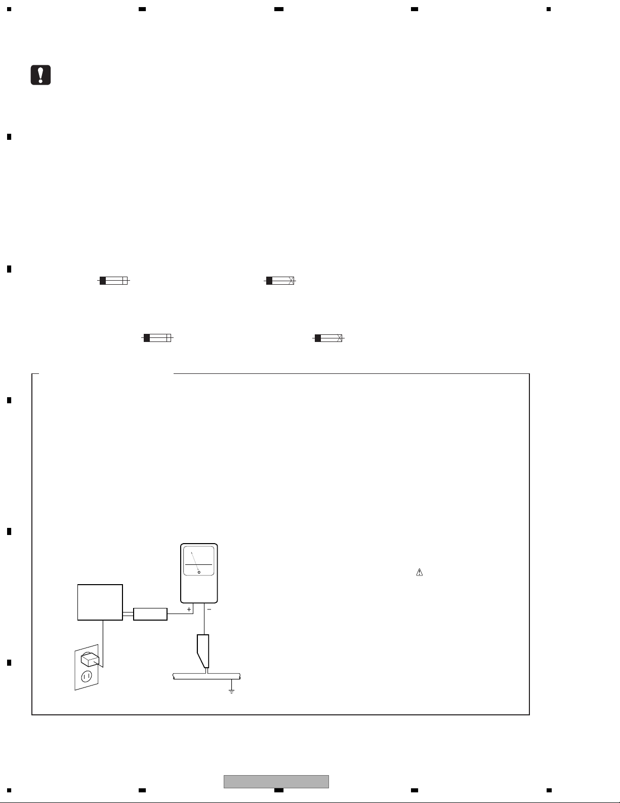
1. SAFETY PRECAUTIONS
The following check should be performed for the
continued protection of the customer and service
technician.
LEAKAGE CURRENT CHECK
Measure leakage current to a known earth ground
(water pipe, conduit, etc.) by connecting a leakage
D
E
current tester such as Simpson Model 229-2 or
equivalent between the earth ground and all exposed
metal parts of the appliance (input/output terminals,
screwheads, metal overlays, control shaft, etc.). Plug
the AC line cord of the appliance directly into a 120V
AC 60 Hz outlet and turn the AC power switch on. Any
current measured must not exceed 0.5 mA.
Reading should
not be above
0.5 mA
Earth
ground
Device
under
test
Also test with
plug reversed
(Using AC adapter
plug as required)
Test all
exposed metal
surfaces
Leakage
current
tester
AC Leakage Test
ANY MEASUREMENTS NOT WITHIN THE
LIMITS OUTLINED ABOVE ARE INDICATIVE
OF A POTENTIAL SHOCK HAZARD AND
MUST BE CORRECTED BEFORE RETURNING THE APPLIANCE TO THE CUSTOMER.
2. PRODUCT SAFETY NOTICE
Many electrical and mechanical parts in the appliance
have special safety related characteristics. These are
often not evident from visual inspection nor the
protection afforded by them necessarily can be obtained
by using replacement components rated for voltage,
wattage, etc. Replacement parts which have these
special safety characteristics are identified in this
Service Manual.
Electrical components having such features are
identified by marking with a
on the parts list in this Service Manual.
The use of a substitute replacement component which
does not have the same safety characteristics as the
PIONEER recommended replacement one, shown in the
parts list in this Service Manual, may create shock, fire,
or other hazards.
Product Safety is continuously under review and new
instructions are issued from time to time. For the latest
information, always consult the current PIONEER
Service Manual. A subscription to, or additional copies
of, PIONEER Service Manual may be obtained at a
nominal charge from PIONEER.
on the schematics and
F
2
1234
XW-HTD630
Page 3
5 678
[ Important symbols for good services ]
In this manual, the symbols shown-below indicate that adjustments, settings or cleaning should be made securely.
When you find the procedures bearing any of the symbols, be sure to fulfill them:
1. Product safety
You should conform to the regulations governing the product (safety, radio and noise, and other regulations), and
should keep the safety during servicing by following the safety instructions described in this manual.
2. Adjustments
To keep the original performances of the product, optimum adjustments or specification confirmation is indispensable.
In accordance with the procedures or instructions described in this manual, adjustments should be performed.
3. Cleaning
For optical pickups, tape-deck heads, lenses and mirrors used in projection monitors, and other parts requiring cleaning,
proper cleaning should be performed to restore their performances.
4. Shipping mode and shipping screws
To protect the product from damages or failures that may be caused during transit, the shipping mode should be set or
the shipping screws should be installed before shipping out in accordance with this manual, if necessary.
A
B
5. Lubricants, glues, and replacement parts
Appropriately applying grease or glue can maintain the product performances. But improper lubrication or applying
glue may lead to failures or troubles in the product. By following the instructions in this manual, be sure to apply the
prescribed grease or glue to proper portions by the appropriate amount.For replacement parts or tools, the prescribed
ones should be used.
C
D
56
XW-HTD630
E
F
7
8
3
Page 4

CONTENTS
SAFETY INFORMATION..................................................................................................................................... 2
A
B
C
D
1. SPECIFICATIONS............................................................................................................................................5
2. EXPLODED VIEWS AND PARTS LIST ............................................................................................................6
2.1 PACKING ................................................................................................................................................... 6
2.2 TRANSMITTER SECTION.........................................................................................................................8
2.3 WIRELESS SPEAKER SECTION........................................................................................................... 10
2.4 AMP SECTION ........................................................................................................................................12
3. BLOCK DIAGRAM AND SCHEMATIC DIAGRAM..........................................................................................14
3.1 BLOCK DIAGRAM................................................................................................................................... 14
3.2 OVERALL WIRING DIAGRAM................................................................................................................. 16
3.3 TX ASSY..................................................................................................................................................18
3.4 MAIN, POWER, FRONT, LED, PRI and RELAY ASSYS..........................................................................20
3.5 AMP and REGULATOR ASSYS .............................................................................................................. 22
3.6 TX MODULE(1/3)..................................................................................................................................... 24
3.7 TX MODULE(2/3)..................................................................................................................................... 26
3.8 TX MODULE(3/3)..................................................................................................................................... 28
3.9 RX MODULE(1/4) ....................................................................................................................................30
3.10 RX MODULE(2/4) ..................................................................................................................................32
3.11 RX MODULE(3/4) ..................................................................................................................................34
3.12 RX MODULE(4/4) ..................................................................................................................................36
3.13 WAVEFORMS........................................................................................................................................38
4. PCB CONNECTION DIAGRAM ..................................................................................................................... 40
4.1 TX ASSY..................................................................................................................................................41
4.2 MAIN ASSY ............................................................................................................................................. 42
4.3 POWER and PRI ASSYS.........................................................................................................................44
4.4 FRONT, LED and RELAY ASSYS............................................................................................................46
4.5 AMP and REGULATOR ASSYS .............................................................................................................. 48
4.6 TX MODULE ............................................................................................................................................50
4.7 RX MODULE............................................................................................................................................ 52
5. PCB PARTS LIST...........................................................................................................................................54
6. ADJUSTMENT ...............................................................................................................................................58
7. GENERAL INFORMATION.............................................................................................................................59
7.1 DIAGNOSIS............................................................................................................................................. 59
7.1.1 TROUBLESHOOTING.......................................................................................................................... 59
7.1.2 NOTES ON REPLACE OF PARTS....................................................................................................... 60
7.1.3 DIAGNOSIS OF THE AMPLIFIER SECTION.......................................................................................60
7.1.4 PROTECTION CIRCUIT.......................................................................................................................61
7.1.5 DISASSEMBLY .....................................................................................................................................63
7.2 IC ............................................................................................................................................................. 67
8. PANEL FACILITIES ........................................................................................................................................76
1234
E
F
4
1234
XW-HTD630
Page 5
General
Transmitter
Wireless Speaker
AC adapter
Amplifier characteristics
RMS(1kHz,THD10%, 4Ω)
Power consumption (without AC adapter)
Power requirements . . . . . . . . . . . . . . .AC120V, 60Hz
Maximum power output . . . . . . . . . . . . . . . . . . 25W/ch
Power requirements . . . . . . . . . . . . . . . . AC120V, 60Hz
Power consumption . . . . . . . . . . . . . . . . . . . . . . . . 8W
AC adapter . . . . . . . . . . . . . . . . . . . . . . . . . . . 1
RCA stereo cord. . . . . . . . . . . . . . . . . . . . . . . . 1
Power consumption . . . . . . . . . . . . . . . . . . . . . . . . .57W
Speaker unit . . . . . . . . . . . . . . . . . . . . .7cm cone type x2
Rated output . . . . . . . . . . . . . . . . . . . . . . . 12V/300mA
. . . . . . . . . . . . . . . . . . . . . . . . . . . . . . . . . . . . . . . . .2W
Input . . . . . . . . . . . . . . . . . . . . . . . . . . . . . . . . .RCA jack
Weight. . . . . . . . . . . . . . . . . . . . . . . . . . . . . . . . . . .0.3kg
Weight. . . . . . . . . . . . . . . . . . . . . . . . . . . . . . . . . . .4.2kg
Dimensions. . . . . . . . . . . . . . .166(W)x56(H)x112(D)mm
Dimensions. . . . . . . . . . . . . .420(W)x178(H)x138(D)mm
Digital Wireless Rear Speaker System
(Transmitter/Wireless speaker)
Accessories
•
This product is intended for household
purposes. Any failure due to use for other
than household purposes (such as longterm use for business purposes in a
restaurant or use in a car or ship) and
which requires repair will be charged for
even in the warranty period.
The specifications and design of this
product are subject to change without
notice, due to improvement.
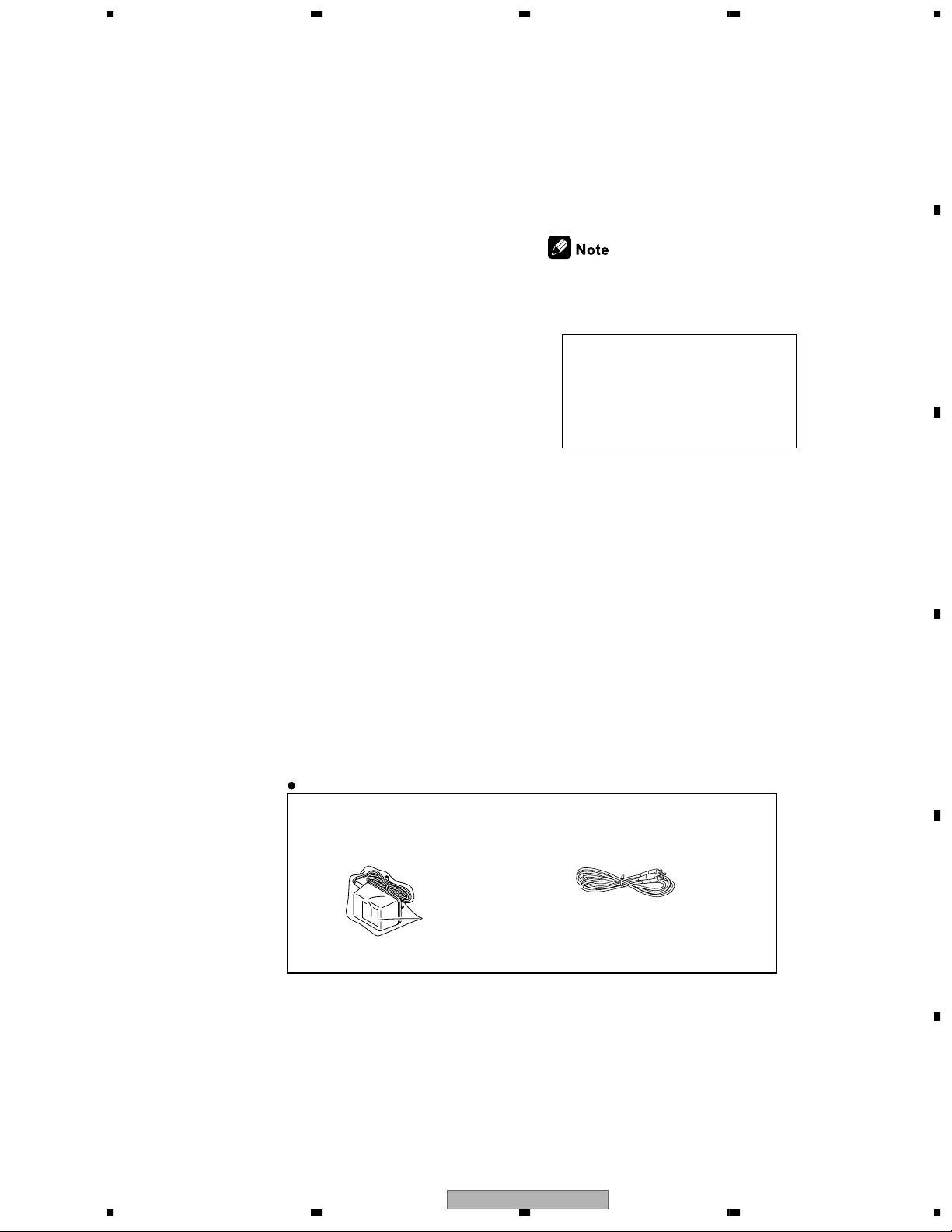
Accessories
• AC Adapter
(AWR7006)
• RCA stereo cord(L=1.5m)
(VDE1064)
5 678
1. SPECIFICATIONS
A
B
C
D
E
F
56
XW-HTD630
7
8
5
Page 6
1234
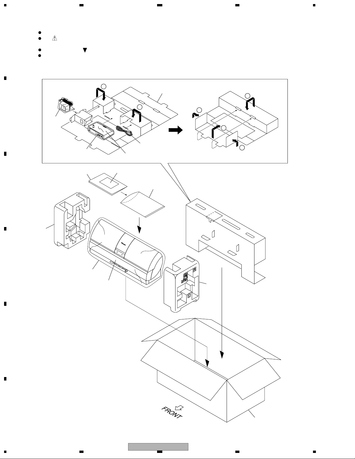
2. EXPLODED VIEWS AND PARTS LIST
NOTES:
A
2.1 PACKING
B
C
Parts marked by "NSP" are generally unavailable because they are not in our Master Spare Parts List.
The mark found on some component parts indicates the importance of the safety factor of the part.
Therefore, when replacing, be sure to use parts of identical designation.
Screws adjacent to mark on product are used for disassembly.
For the applying amount of lubricants or glue, follow the instructions in this manual.
(In the case of no amount instructions, apply as you think it appropriate.)
1
2
2
3
4
5
Transmitter
13
1
3
4
4
4
8
10
D
E
9
Wireless Speaker
11
F
6
1234
XW-HTD630
12
Page 7

5 678
PACKING parts List
Mark No. Description Part No.
1 Accessory Box AHB7083
2AC Adapter AWR7006
3 RCA Stereo Cord VDE1064
NSP 4 Literature Bag AHG1180
5 Operating Instructions ARC7475
(English, French)
6• • • • • • • •
7• • • • • • • •
NSP 8 Polyethylene Bag Z21-038
9Packing Sheet (large) AHG7010
10 Pad L AHA7414
11 Pad R AHA7415
12 Packing Case AHD8215
NSP 13 Warranty Card ARY7045
A
B
C
D
E
56
XW-HTD630
F
7
8
7
Page 8
1234
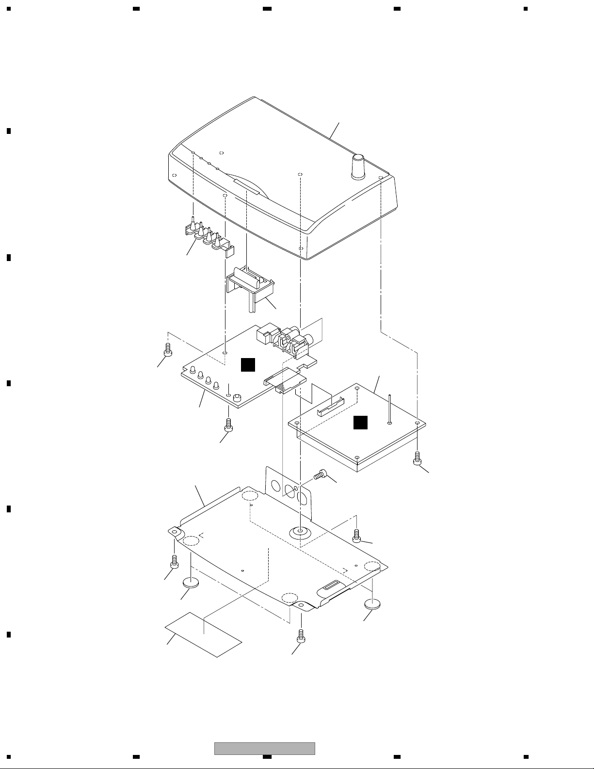
2.2 TRANSMITTER SECTION
A
B
3
4
C
8
1
A
5
2
J
D
E
8
8
6
8
8
8
7
7
9
F
8
1234
XW-HTD630
8
Page 9

5 678
TRANSMITTER SECTION parts List
Mark No. Description Part No.
1 TX Assy AWU8120
2 TX Module AXF7006
3Top Panel AAK8172
4 CS Lens AAK8133
5 CS Button T AAD7712
6 Chassis T ANA7157
7 Leg AEB7090
8 Screw
NSP 9 Name Label T AAL7330
*
ABA7097
A
*
Use TORX driver GGK1028.
B
C
D
56
XW-HTD630
E
F
7
8
9
Page 10
1234
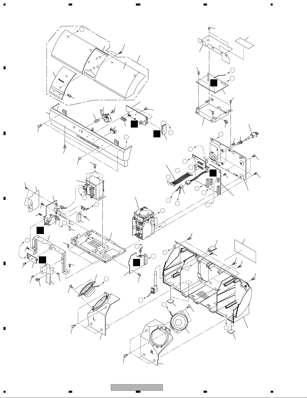
2.3 WIRELESS SPEAKER SECTION
A
A
41
39
50
42
38
24
47
22
56
P
O
K
47
B
36
49
7
14
23
C
21
31
30
48
47
17
1
52
46
49
46
46
40
15
44
32
9
I
F
H
55
46
47
10
25
22
12
34
45
35
33
B
Refer to
"2.4 AMP SECTION".
16
D
2
D
8
C
47
3
48
G
I
L
P
J
6
F
H
E
20
G
O
11
C
13
J
D
K
N
A
E
47
19
54
L
K
N
46
46
B
37
46
C
22
26
5
47
47
D
G
47
F
51
18
48
E
47 4
22
23
E
27
22
B
46
28
F
(
10
1234
46
XW-HTD630
29
12
43
20
Page 11

>
>
>
5 678
WIRELESS SPEAKER SECTION parts List
Mark No. Description Part No.
1 MAIN Assy AWU8121
2POWER Assy AWU8122
3FRONT Assy AWU8123
4 LED Assy AWU8124
5 PRI Assy AWU8125
Mark
No. Description Part No.
51 UL T ube ADN7011
NSP 52 Name Label AAL7322
53 • • • • • • •
54 • • • • • • •
NSP 55 Fuse Card AAX7520
A
6 RELAY Assy AWU8126
7 RX Module AXF7008
NSP 8 AMP Module L-2CH AXQ7249
9Power Transf ormer (T1) A TS7366
10 Fuse (FU1 : 1.6A) REK1110
11 4P Cable Assy ADX7431
12 Speaker B70AC50-51C
13 13P Connector Assy PG13KK-G22
14 Power Cord VDG1075
15 Spring P ABH7231
16 Chassis ANA7156
17 Rear Panel ANC8184
18 PCB Angle ANG7464
19 Shield Cover A ANK7112
20 Rubber Leg AEB7318
NSP 21 PCB Spacer (3 x 6) AEC7156
22 Push Rivet AEC7221
23 Mini Clamp AEC7373
24 Top Barrier AEC7474
25 Fuse Barrier AEC7475
26 Primary Barrier AEC7476
27 Front Barrier AEC7484
28 Baffle L AMD7009
29 Baffle R AMD7010
30 Strain Relief CM-22C
56 65 Label ARW7050
B
C
D
NSP 31 PC Support VEC1749
32 MIC Knob AAB7262
33 Slide Knob AAC7052
34 Power Button AAD7710
35 CS Button AAD7711
36 Antenna Cover AAK8142
37 Front Panel AMB7855
38 Grille Assy AXG7209
39 Center Panel AAK8171
40 Auto Lens AAK8131
NSP 41 SP Grille AAK8146
NSP 42 Jersey Net AAR7010
43 Rear Case Assy AXG7210
44 Screw BBZ40P060FMC
45 Screw IPZ30P080FMC
46 Screw BPZ40P100FZK
47 Screw BBZ30P060FMC
48 Screw BPZ30P080FZK
49 Screw BBZ30P080FNI
50 Screw BPZ30P080FMC
56
XW-HTD630
E
F
7
8
11
Page 12
1234
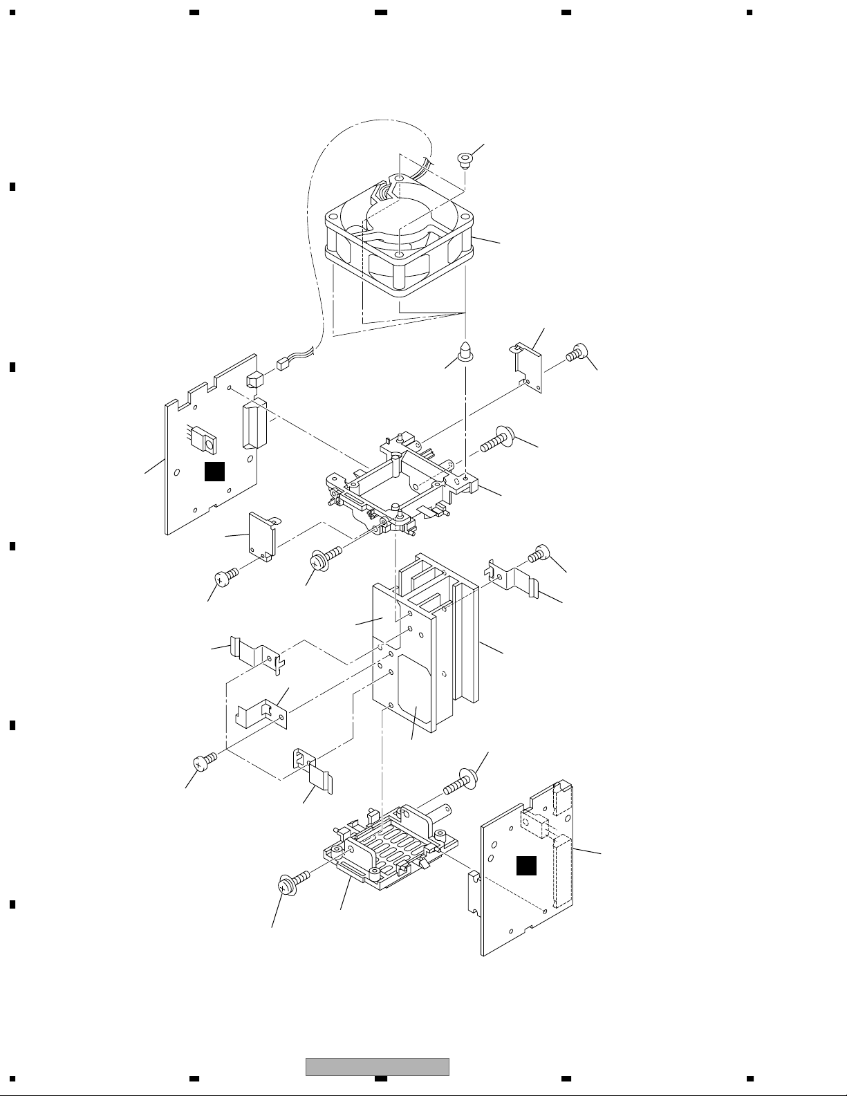
2.4 AMP SECTION
A
B
7
3
8
7
C
14
I
8
13
12
9
10
11
13
2
D
13
5
4
14
15
9
15
E
9
1
H
6
13
F
12
1234
XW-HTD630
Page 13

5 678
AMP SECTION parts List
Mark No. Description Part No.
1 AMP Assy AWU7968
2 REGULATOR Assy AWU7969
3 DC Fan Motor AXM7025
4 Heat Sink ANH7169
5Fan Mold AMR7470
6 Rear Mold AMR7437
7 Insulation Rubber AEB7256
8 Insulation Plate AND7055
9 FET Bracket A ANG7432
10 PCB Holder ANG7472
A
11 Mica Sheet A AEE7049
12 Mica Sheet B AEE7050
13 Screw ABA1021
14 Screw BPZ30P080FZK
15 Screw BBZ30P060FMC
B
C
D
56
XW-HTD630
E
F
7
8
13
Page 14
1234
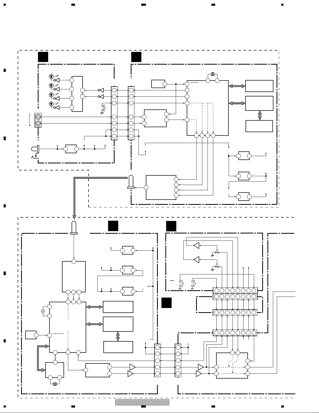
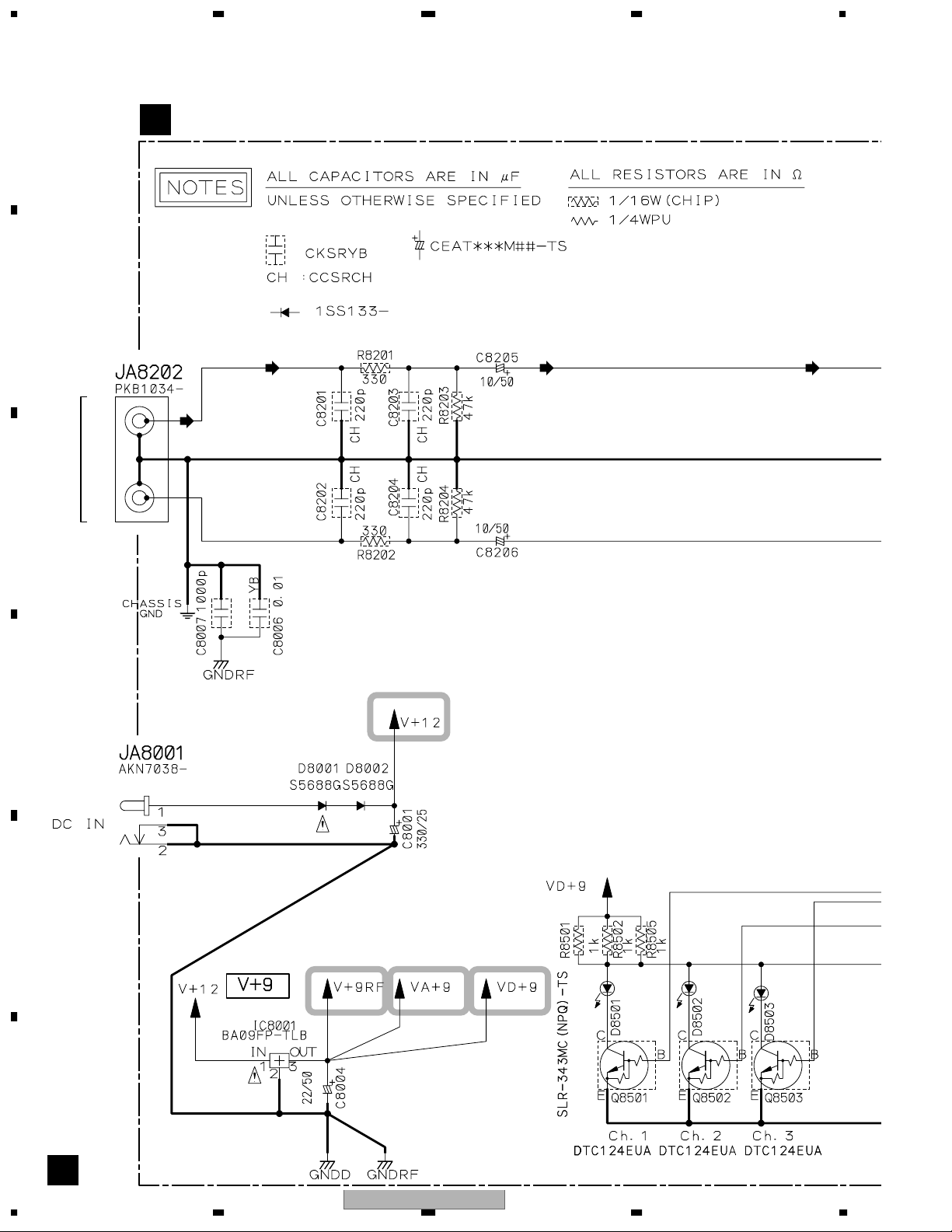
3. BLOCK DIAGRAM AND SCHEMATIC DIAGRAM
3.1 BLOCK DIAGRAM
A
TRANSMITTER SECTION
TX ASSY
A
IC8501
BU4052BCF
Ch.1
Ch.2
Ch.3
B
Ch.4
JA8202
L
R
INPUT
WIRERESS
JA8001
DC IN
C
Ch Select SW.
Q8501
11
Q8502
15
9
14
12
IC8001
BA09FP
10
Q8503
Q8504
9V REG.
V+12 V+9RF
1 3
Q8506
Q8505
Ch. select
VA+9
CN8201
VD+9
(12P)H2(12P)
LED 2
3
LED 1
4
CHSEL
2
LIN
6
RIN
8
V+9RF
11
V+9RF
12
ANT1
TX MODULE
J
Power On Reset
PLD02
3
PLD01
4
CHANNELSEL
2
6
8
11
12
AINL
2
AINR
1
AK5380VT
A/D Converter
+9V
12
U3
KIA7021AF
System
SDTO
U9
U23
RFTXMODAIR
RF Tx Module
RFINANT
3
13
9
DATA
CHAN2
CHAN1
CHAN3
X1
24.576MHz
RESET
11
PLD02
71
PLD01
70
CHNNELSEL
8
SDTO
76
1
8
9
7
3 5
CLKIN CLKOUT
FS2103TX
Freesystems
Tx Chip
RFOUT
CHANNEL1
CHANNEL2
51 53 54 55
U1
CHANNEL3
AD0-AD11
NCP1117ST50T3
REG.
+9V
3 2
NCP1117ST50T3
5V REG.
3 2
NCP1117ST33T3
3.3V REG.
D5V
3 2
IC61LV256-12T
SRAM for FS
52806-0910
EEPROM Prog.
Interface
EEPROM for FS
U21
U6
U22
U5
H10
U7
RFSUPPLY+
A5V
D3V3
RX MODULE
K
FRONT ASSY
D
ANT2
D
D5V
17
RFANT2
U16
RFRX
RF Rx Module
DATA6CHAN18CHAN4
11
54
55
49
CLKIN
RFINSDTI
CLKOUT
U2
FS2103RX
Freesystems Rx Chip
RESETIN
VCLKIN
71 8
62
6
U18
VCXO
X2
3
11
VCXO1-VCXO8
MK3711D
12.288MHz
3
5
1 8
E
X3
24.576MHz
U20
KIA7021AF
System Reset
F
CHANNEL3
CHANNEL2
CHANNELSCAN
2
AD0-AD11
DATA
PCM1742KE
D/A Converter
D3V3
A3V3
A5V
D5V
IS61LV256-12T
SRAM for FS
52807-0910MOLEX
EEPROM Prog.
EEPROM for FS
VOUTL
7
VOUTR
8
U28
U12
NCP1117ST50T3
5V REG.
2 3
U19
NCP1117ST33T3
3.3V REG.
2 3
U17
NCP1117ST50T3
5V REG.
2 3
U4
H6
Interface
U11
3
NJM4558
DAC Filter
RFSUPPLY+
+9V
+9V V+9RF
12
CHANNELSCAN
7
5
1
U24
11
H3
(12P)
1
8
6
SURROUND
G
V+9
V+9
CH. select
LOUT
ROUT
NJM4558MD
STEREO
Ch. select
RELAY
ASSY
1
2
12
5
7
CN3701
(12P)
5
7
IC3051
3
1
CN3504
CN3503
CN3502
CN3051
1
3
7
5
IC3301
NJM4558MD
VR3051
VOL
(13P)
3 7 5 9 11 1
3 7 5 9 11 1
(13P)
(13P)
11 7 9 5 3 13
LVIN
RVIN
CH. select
11 7 9 5 3 13
(13P)
X0
12
Y0
1
IC3001
BU4052BCF
E. VOL
LVOUT
RVOUT
5 14
Y1 X1
X (Lch)
Y (Rch)
2
2
12
VA+9
12
VA+9
VREF
VA+9
9
13
3
VREF
13
13
1
Mode
1
VREF
14
1234
XW-HTD630
Page 15
5 678
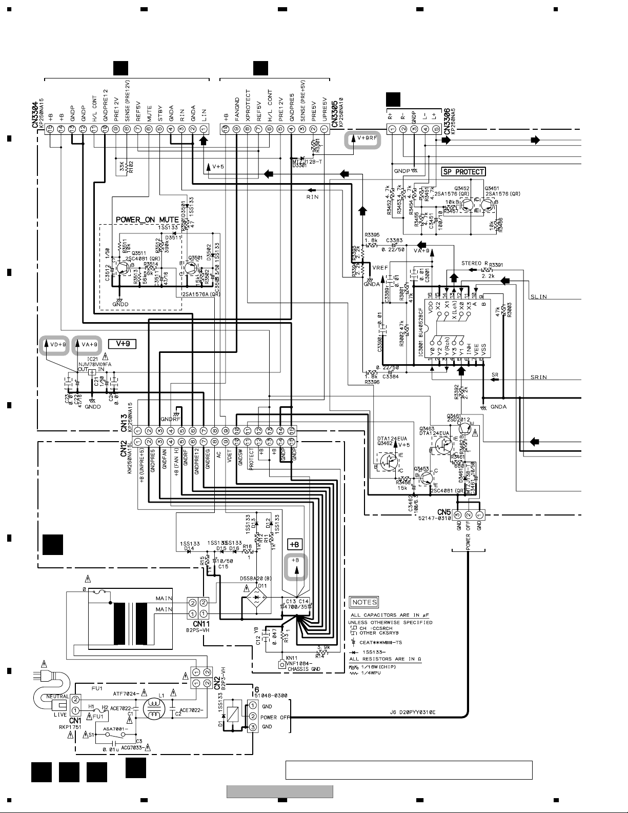
SPEAKER SECTION
A
B
VREF
POWER ASSY
C
D13
D16
D15
D14
CN12
(15P)
1 4 8 9 12
AC
+B (FAN H)
+B (UNPRE+5)
1 4 8 9 12
CN13
(15P)
IC21
NJM78M09FA
VA+9VD+9
9V REG.
CN11
+B
D11
D12
13
11
+B
+B
VDET
PROTECT
13 2
11
AMP MODULE L-2CH
H
LIN
RIN
MUTE
+B
+B
1
3
6
7
9
14
15
CN3302
(15P)
1
3
6
7
9
14
15
CN3304
(15P)
REF5V
PRE12V
MAIN
2
MAIN
121
POWER OFF
CN5
(3P)
AMP ASSY
REF5V
PRE REG.
+B
Circuit
for +12V
T1
POWER
TRANSFORMER
POWER OFF
L IN
R IN
PRE12V VP
1
13
TDA8560Q
Power Amp.
Q3305
F
1
2
2
6
(3P)
IC3301
11
D1
MODE
PRI ASSY
CN1CN2
NEUTRAL
LIVE
FU1
B
L +OUT
CN3301
(5P)
5
4
1
2
R +OUT
9
4
AC IN
2
1
MAIN ASSY
CN3306
(5P)
5
4
1
2
J3401
L +
L R +
R-
INSIDE
SPEAKER
C
D
E
V+9RF
REGULATOR ASSY
I
V+5
Q3462
CN3305
(10P)
1
2
7
5
8
10
UPRE5V
PRE5V
REF5V
PRE12V
XPROTECT
+B
CN3303
(10P)
1
2
7
5
8
10
UPRE5V
PRE12V
+B
CN3651
PRE REG.
Circuit
for +5V
Short DET.
FAN DET.
1
2
XW-HTD630
56
DC FAN
MOTOR
F
7
8
15
Page 16
1234
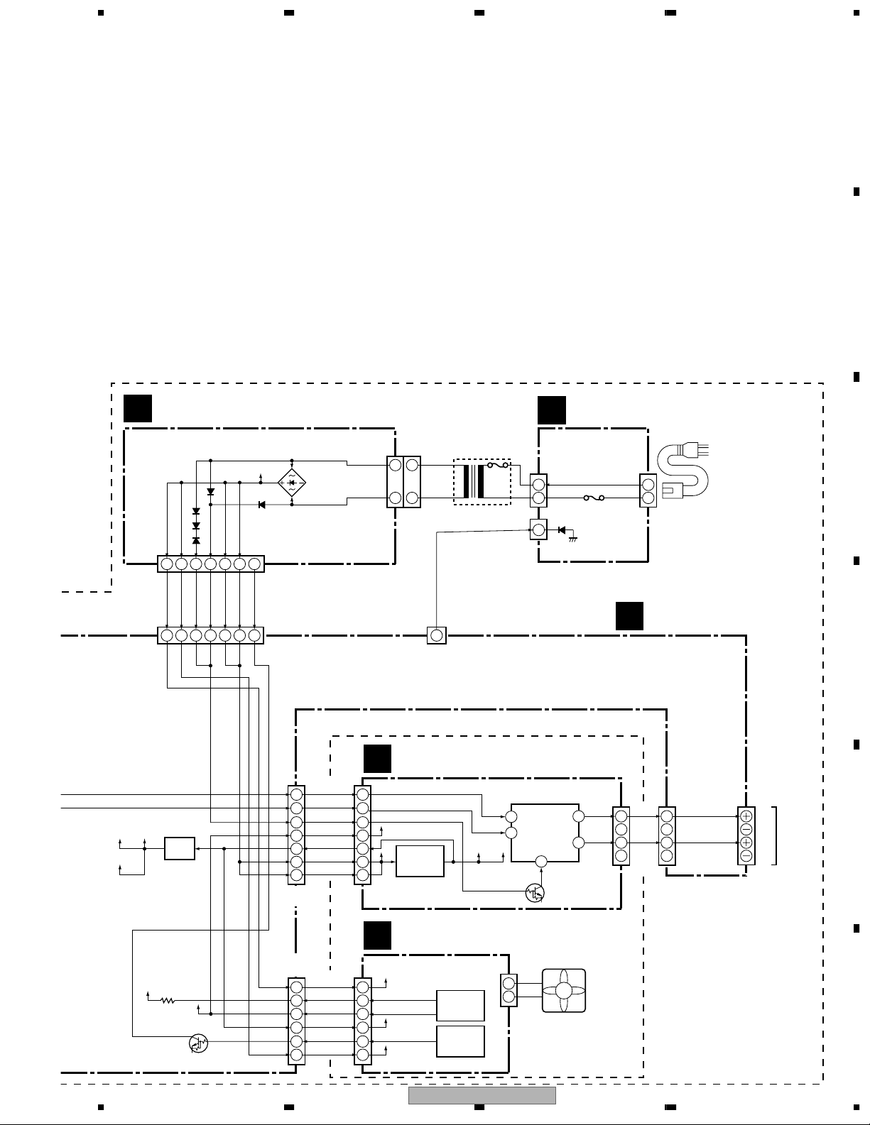
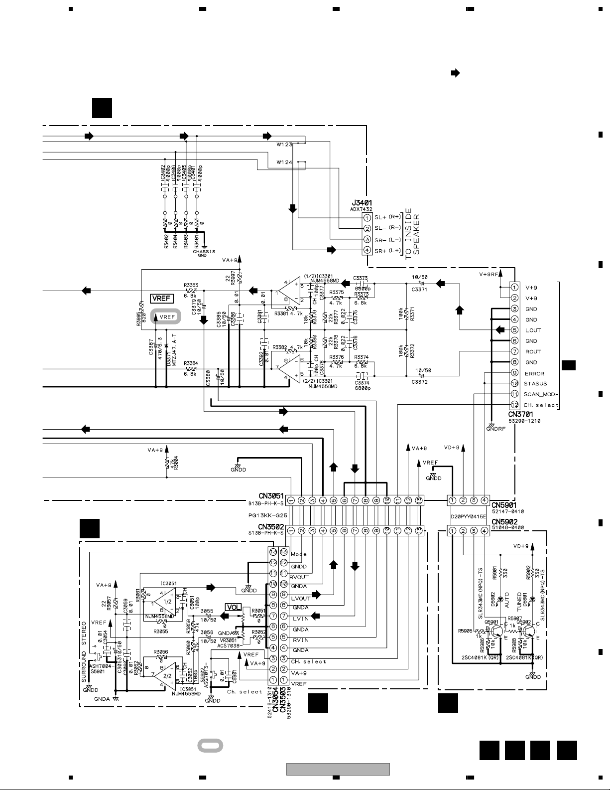
3.2 OVERALL WIRING DIAGRAM
A
• Transmitter Section
WIRERESS
INPUT
DC IN
B
• Speaker Section
C
R
L
JA8202
JA8001
A
TX ASSY
(AWU8120)
CN8201 H2
STATUS (NC)
1
2
3
4
5
6
7
8
9
10
11
12
CHSEL
LED 2
LED 1
GND
LIN
GNDA
RIN
GNDRF
GNDRF
V+9RF
V+9RF
1
2
3
4
5
6
7
8
9
10
11
12
J
TX MODULE
(AXF7006)
K
RX MODULE
(AXF7008)
H3
12 11 10 9
8 7
ANT1
ANT2
2
3
5
6
1
4
D
E
F
POWER CORD
: VDG1075
CN1
NEUTRAL
2
LIVE
1
CN5
1 2 3
J6
GND
GND
POWER OFF
1 2
3
6
F
PRI ASSY
(AWU8125)
CN2
POWER
TRANSFORMER
: ATS7366
1
2
V+9
V+9
GND3GND
GND
LOUT
ROUT
5
6
CN3701
1
2
7
4
B
MAIN ASSY (AWU8121)
CN13
1 2
3 4
GNDFAN
GNDPRE5
+B (FAN H)
+B (UNPRE+5)
1
2
3
CN12
T1
CN11
212
1
4
C
POWER ASSY
(AWU8122)
GND
8
5 6 7
GNDRF
GNDPRE12
5
6
ERROR
STATUS
10
9
8
AC
GNDREG
8
7
CH. select
SCAN_MODE
11
12
11 13 14 15
10
9
VDET
GNDSW
PROTECT
11+B13
10
9
12
+B
GNDP14GNDP
15
12
16
1234
XW-HTD630
Page 17
5 678
Note : When ordering service parts, be sure to refer to "EXPLODED VIEWS and PARTS LIST" or "PCB PARTS LIST".
AMP MODULE L-2CH (AXQ7249)
A
B
CN3051
CN3502
CN3302
GNDA
2
RIN
3
GNDA
4
5 6
STBY
5
MUTE
6
1 2 3 4
LIN
1
CN3304
1 2
Mode
1
GNDD
2
3 4
GNDA
RVOUT
3
4
5 6 7
LVOUT
5
G
RELAY ASSY
(AWU8126)
H
AMP ASSY
(AWU7968)
11 13 14 15
10
9
PRE12V
GNDPRE12V
10
9
8
9
RVIN
GNDA
8
9
12
H/L CONT
11
12
11 13
10
GNDA
CH. select
11
10
GNDP
13+B14+B15
12
VA+9
12
8
7
REF5V
SENSE (PRE12V)
8
7
LVIN
GNDA
6
7
CN3301
5
L+
R–
GNDP
5
2
3L–4
GNDP
1 2 3 4
R+
1
CN3306
VREF
13
CN3503 CN3054
Mode
13
GNDD
12
RVOUT
11
GNDA
10
LVOUT
9
GNDA
8
7
GNDA
6
5
GNDA
4
CH. select
3
2
1
LVIN
RVIN
VA+9
VREF
13
12
11
10
9
8
D
7
6
FRONT ASSY
5
(AWU8123)
4
3
2
1
I
REGULATOR ASSY
(AWU7969)
CN3303
1 2 3 4
PRE5V
UPRE5V
1
2
CN3305
5 6
PRE12V
H/L CONT
GNDPRE5
SENSE (PRE+5V)
5
6
3
4
8
7
REF5V
XPROTECT
8
7
10
9
+B
FANGND
10
9
CN5901
J5902
CN5902
CN3651
J3401
SL+ (R+)
SL– (R–)
SR– (L–)
SR+ (L+)
1 2
3 4
VD+9
GNDD
SCAN_MODE
ERROR/STATUS
1
2
3
4
E
LED ASSY
(AWU8124)
DC FAN
MOTOR
+
1
–
2
C
D
R ch
SPEAKER
1
2
3
4
: B70AC50-51C
L ch
SPEAKER
: B70AC50-51C
E
F
56
XW-HTD630
7
8
17
Page 18
1234
3.3 TX ASSY
A
B
L
INPUT
WIRERESS
C
L
TX ASSY (AWU8120)
A
D
E
F
18
A
XW-HTD630
1234
Page 19
5 678
: AUDIO SIGNAL ROUTE (L ch)
: The power supply is shown with the marked box.
A
B
H2
J 2/3
C
CH Select SW.
D
E
Switches
S8901 : Ch. select
F
56
XW-HTD630
A
7
8
19
Page 20
1234
3.4 MAIN, POWER, FRONT, LED, PRI and RELAY ASSYS
CN3302
A
B
H
CN3303
I
H
CN3301
E. VOL.
C
D
E
F
B C F
20
POWER ASSY
C
(AWU8122)
POWER TRANSFORMER
POWER CORD
VDG1075
REK1110
1.6A
1234
T1
ATS7366
F
PRI ASSY (AWU8125)
XW-HTD630
• NOTE FOR FUSE REPLACEMENT
CAUTION -
FOR CONTINUED PROTECTION AGAINST RISK OF FIRE.
REPLACE WITH SAME TYPE AND RATINGS ONLY.
Page 21
5 678
MAIN ASSY (AWU8121)
B
: AUDIO SIGNAL ROUTE (L ch)
A
B
C
H3
FRONT ASSY (AWU8123)
D
K 2/4
D
J5902
E
Switches
S5901 : SURROUND/STEREO
S5902 : Ch.select
56
RELAY ASSY
G
(AWU8126)
: The power supply is shown with the marked box.
XW-HTD630
7
LED ASSY
E
(AWU8124)
F
EDB G
21
8
Page 22
1234
3.5 AMP and REGULATOR ASSYS
A
B
C
REGULATOR ASSY (AWU7969)
I
14.7V
D
8.4V
16.4V
B
CN3305
26.4V
E
MOTOR
DC FAN
F
I
22
1234
XW-HTD630
Page 23
5 678
B
CN3306
: The power supply is shown with the marked box.
: AUDIO SIGNAL ROUTE (L ch)
AMP ASSY (AWU7968)
H
A
B
C
B
CN3304
D
E
F
56
XW-HTD630
H
7
8
23
Page 24

1234
3.6 TX MODULE(1/3)
A
J 1/3
B
C
TX MODULE(1/3) (AXF7006)
2/3
J
3/3
J
3/3
J
2/3
J
3/3
J
Note
L7
VTL1067
D
3/3
J
3/3
J
E
33pF
R49SDA-024576-F1-25C
33pF
3/3
J
2/3
J
2/3
24
J
J
1/3
XW-HTD630
1234
F
Page 25

5 678
A
2/3
J
B
2/3
J
3/3
J
Note
L6
VTL1067
C
2/3
J
D
E
Note : At this block, the assembled parts
2/3
J
is different from the PCB silk.
PCB
Assembled
Silk
Parts
R 6 ← L 6
R 7 ← L 7
56
XW-HTD630
F
J
1/3
7
8
25
Page 26

1234
3.7 TX MODULE(2/3)
A
J 2/3
B
A
C
TX MODULE(2/3) (AXF7006)
CN8201
H 2
J
3/3
J
3/3
J
1/3
J
3/3
D
J
1/3,3/3
E
J
1/3
J
1/3
J
F
1/3
J
3/3
26
J
2/3
XW-HTD630
1234
Page 27

5 678
: The power supply is shown with the marked box.
J
3/3
J
1/3
A
B
C
J
1/3
D
E
J
3/3
J
1/3
56
XW-HTD630
F
J
2/3
7
8
27
Page 28

1234
3.8 TX MODULE(3/3)
A
B
C
J 3/3
TX MODULE(3/3) (AXF7006)
J
2/3
J
2/3
D
E
Note
J
2/3
S5688G
F
L43
QTL1011
470pF
28
J
3/3
XW-HTD630
1234
Page 29
5 678
A
B
Note
L15
VTL1067
L16
VTL1067
J
1/3
J
J
1/3
1/3,2/3
2
4
3
Note
J
1/3
J
1/3
L74
VTL1067
J
1/3
C
1
D
J
1/3
J
1/3
Note : At this block, the assembled parts
is different from the PCB silk.
PCB
Assembled
Silk
Parts
R15 ← L15
R16 ← L16
R43 ← L43
R74 ← L74
: The power supply is shown with the marked box.
56
XW-HTD630
E
F
J
3/3
7
8
29
Page 30

1234
3.9 RX MODULE(1/4)
A
B
C
K 1/4
K
RX MODULE(1/4) (AXF7008)
3/4
1pF
A49US-12288FA-14-30A
Note
1pF
L71
VTL1067
K
3/4
Note
L9
VTL1067
K
K
2/4
2/4
K
3/4
D
K
2/4
E
K
3/4
K
3/4
K
3/4
F
1/4
K
30
1234
XW-HTD630
Page 31

5 678
A
K
3/4
K
K
2/4
K
3/4
2/4
K
2/4
Note
L8
VTL1067
K
B
3/4
C
K
2/4
K
2/4
K
K
2/4
2/4
K
2/4
Note : At this block, the assembled parts
is different from the PCB silk.
PCB
Assembled
Silk
Parts
R 8 ← L 8
R 9 ← L9
R71 ← L71
XW-HTD630
R49SDA-024576-F1-25C
56
K
2/4
K
3/4
K
2/4
K
2/4
D
K
2/4
E
F
K
1/4
7
8
31
Page 32

1234
3.10 RX MODULE(2/4)
A
B
C
K 2/4
CN3701
B
RX MODULE(2/4) (AXF7008)
H3
K
4/4
K
1/4
D
K
3/4
E
K
1/4
K
1/4
K
1/4
F
32
K
2/4
XW-HTD630
1234
Page 33

5 678
: The power supply is shown with the marked box.
K
1/4
K
K
1/4
A
3/4
B
C
K
1/4
K
1/4
K
3/4
K
D
E
3/4
56
XW-HTD630
F
K
2/4
7
8
33
Page 34

1234
3.11 RX MODULE(3/4)
A
B
K
1/4
C
D
Note Note
L104
K
VTL1067
4
4/4
3
2
L105
VTL1067
K
1/4
E
K
2/4
S5688G
470pF
F
: The power supply is shown with the marked box.
34
K
3/4
XW-HTD630
1234
Note
L41
QTL1011
Page 35

5 678
A
K
K
1/4
1/4
K
1/4
K
K
1/4
1/4
K
1/4
K 3/4
RX MODULE(3/4) (AXF7008)
B
1
C
Note : At this block, the assembled parts
is different from the PCB silk.
PCB
Assembled
Silk
Parts
R41 ← L41
R104 ← L104
R105 ← L105
D
E
F
56
XW-HTD630
K
3/4
7
8
35
Page 36

1234
3.12 RX MODULE(4/4)
A
K 4/4
B
C
RX MODULE(4/4) (AXF7008)
K
3/4
K
3/4
D
E
F
36
K
4/4
XW-HTD630
1234
Page 37

5 678
A
K
2/4
K
B
C
2/4
D
56
XW-HTD630
E
F
K
4/4
7
8
37
Page 38

1234
3.13 WAVEFORMS
A
TX MODULE
J
U23-Pin1
1
V : 2V/div. H : 500nsec/div.
B
U9-Pin12
2
V : 2V/div. H : 200nsec/div.
C
Note : The encircled numbers denote measuring point in the schematic diagram.
RX MODULE
K
U9-Pin10
4
V : 2V/div. H : 10µsec/div.
U16-Pin6
1
V : 2V/div. H : 500nsec/div.
U28-Pin1
2
V : 2V/div. H : 200nsec/div.
U28-Pin3
4
V : 2V/div. H : 10µsec/div.
U9-Pin9
3
V : 2V/div. H : 1µsec/div.
D
E
U282-Pin2
3
V : 2V/div. H : 2µsec/div.
F
38
1234
XW-HTD630
Page 39

5 678
A
B
C
D
E
56
XW-HTD630
F
7
8
39
Page 40

1234
4. PCB CONNECTION DIAGRAM
NOTE FOR PCB DIAGRAMS :
A
1. Part numbers in PCB diagrams match those in the schematic
diagrams.
2. A comparison between the main parts of PCB and schematic
diagrams is shown below.
Symbol In PCB
Diagrams
BCE
BCE
B
D
Symbol In Schematic
Diagrams
BCEBCE
BCE
DGGSS
BCE
DGS
Part Name
Transistor
Transistor
with resistor
Field effect
transistor
Resistor array
3-terminal
regulator
3. The parts mounted on this PCB include all necessary parts for
several destinations.
For further information for respective destinations, be sure to
check with the schematic diagram.
4. View point of PCB diagrams.
Connector
Capacitor
SIDE A
P.C.Board
Chip Part
SIDE B
C
D
E
F
40
1234
XW-HTD630
Page 41

5 678
16
1
9
8
LF
R8101
R8103
IC8101
R8105
R8109
R8111
R8113
R8115
R8117
R8119
R8107
R8121
R8127
R8123
R8125
C8201L8201
R8205
R8201
C8203
R8203
R8204
C8204
R8202
C8202
R8206 R8211
L8202
L8211
R8126
R8128
R8122
R8124
R8116
R8120
R8118
R8114
R8112
R8110
R8108
IC8102
R8106
R8102
L8001
L8002
C8003
IC8001
C8002
R8001
R8002
C8113
R8129
R8130
C8114
IC8501
R8501
R8133
R8134
R8104
R8502
C8501
C8901
R8231
R8232
Q8501
Q8502
Q8503
Q8504
Q8505
Q8506
Q8103
Q8104
Q8106
Q8105
Q8102
Q8101
R8503
R8504
C8005
R9001
C8006
C8007
R8505
C8010
C8009
GNDA
GNDA
5
4
1
8
5
4
1
8
VA+9
VREF
VREF
GNDA
VA+9
V+9RF
Ch.1
GNDD
GNDD
VA+9
GND
NC
Ch.SEL
LED2
LED1
GND
LIN
GND
RIN
GNDRF
V+9RF
V+9RF
1
12
TX ASSY
PNE-1B1
GNDRF
GNDRF
RIN
112
112
C8101
C8103 C8109
D8101
D8103
C8107
C8105
JA8001
C8205
C8206
D8102
C8108
D8104
C8110
C8106
C8104
C8102
C8115
C8116
D8001
C8004
C8001
S8901
D8504
D8503
D8502
C8111
C8112
D8501
C8008
D8004
CN8201
W163
W165
W147
W167
W134
W162
W133
W197
W161
JA8202
W196
W185
W146
W181
W166
W183
W182
W145
W160
W184
W159
W164
W132
W131
W130
D8002
GNDA
GNDA
PNE-1B1
VA+9
GNDA
V+9RF
Ch.1
GNDD
VREF
LIN
VA+9
VA+9
VREF
GNDD
GND
AWU8120
TX ASSY
Channel
Ch.4 Ch.3
Ch.2
Ch.1
GNDRF
GNDRF
RIN
AWU
SIDE A SIDE A
SIDE B SIDE B
A A
TX ASSY
A
TX ASSY
A
H2
J
(ANP7484-B)
(ANP7484-B)
CN8201
CN8201
Q8504
Q8503
Q8502
Q8501
IC8501
IC8101
IC8102
Q8505
Q8506
Q8106
Q8104
Q8103
Q8105 Q8101
Q8102
4.1 TX ASSY
A
B
C
56
XW-HTD630
7
D
E
F
41
8
Page 42

1234
4.2 MAIN ASSY
SIDE A SIDE A
A
6
F
MAIN ASSY
B
C3512
B
W189
MUTE
R3511
C3501
D3511
D3502
D3501
C3462
C3461
R3513
C3511
C3385
W179
W178
5
GNDA
VREF
W157
W154
W153
C
C22
C21
Q3461
IC21
W187
D3461
IC21
Q3461
W188
PRINTED SIDE
PRE12V
15
15
+B
D21
V+9RF
W174
SIDEPRINTED
15
1
J3307
C3371
GNDRF
V+9RF
C3372
C3380
C3379
W177
GNDA
W176
W175
VD+9
GNDRF
W151
W150
W173
1
1
CN13
W149
D
PRE12V
W172
W152
VD+9
R+
W156
W136
CN5J3307
VREF
3
3
CN5
R-
W155
GNDP
W143
C3387
C3383C3384
1
1
L+
W142
C3451
D3371
CN3305
R3393
R3394
110
D3301
110
W135
PROTECT
W192
GNDS
W148
PROTECT
STBY
W186
H/L CONT
+B
GNDPRE12
GNDP
W170
W171
W168
E
W203
R103
GNDS
W169
W202
GNDS
L-
W141
CN3502
G
CN3051
V+9RF
W140
VA+9
W139
R-
GNDP
W138
W137
1
12
CN3051
13
13
White
1
4
4
J3401
W122
W121
R-
W120
VREF
W127
Ch.SEL
W126
L-
1
W125
1
1
1
PNE-1B1
12
12
S3401
W124
W123
EXCEPT
/KUC
GNDS
CN3701
W195
W194
W193
AWU
DC FC
1
1
4
4
CN5901
L
GND
R
service
for
AWU8121
W201
W200
1
pin
CN5901
CN3701
J3401
AWU8127
CN5902
E
H3
K
SPEAKER
C
CN13
CN12
1
1
R102
15
15
CN3304
CN3304
CN3302
H
CN3305
CN3303
I
MAIN ASSY
1
15
5
CN3306
CN3306
CN3301
H
Production code
(ANP7484-B)
F
B B
42
1234
XW-HTD630
Page 43

5 678
16
1
9
8
41
1
15
1
LF
R3301
R101
R3502
R3501
R3512
R3372
R3385R3386
C3386
R3371
R3997
R3004
R3402
R3401
R3403
R3404
C3401
C3406
C3405
C3402
R3405
R3406
C3403
C3407
C3408
C3404
IC3001
R3003
R3382
C3378
C3374
R3374
R3376
IC3301
R3379R3380
C3376 C3375
R3377R3378
R3381
C3377
C3373
R3375
R3373
R3453
R3454
R3451
R3452
R3455
R3383
R3384
R3456
R3514
R3001
R3002
C3001
R3391
R3392
R3457
R3995
R3996
Q3451
Q3452
Q3462
R3461
R3458
Q3453
Q3511
Q3501
Q3463
R3462
C3396
C3381
R3395
C3382
C26
C25
C3395
C3393
C3394
C3389
C3390
C3391
C3392
C24
C23
R3396
C3701
GNDS
1
2.R-
GNDS
R-
1.R+
5
VA+9
GNDPRE12
9.VDET
7.GNDREG
6.GNDPRE12
5.GNDRF
3.FANGND
4.FAN H
10.GNDSW
2.GNDPRE5
11.PROTECT
+B
+B
GNDP
14.GNDP
15.GNDP
12.+B
13.+B
1.UNPRE5
4.GNDA
1.LIN
2.GNDA
3.RIN
5.STBY
6.MUTE
7.REF5V
8.SENSE
9.PRE12V
10.GNDPRE12
11.H/L CONT
12.GNDP
13.GNDP
14.+B
15.+B
5
41
8
1.UNPRE5V
2.PRE5V
3.SENSE
4.GNDPRE5
5.PRE12V
6.H/L CONT
7.REF5V
8.XPROTECT
9.FANGND
10.+B
3.GNDP
4.L-
5.L+
L-
L+
GNDP
R-
R+
1
3.GNDSW
5
2.P OFF
1.GNDSW
Mode
GNDD
RVOUT
GNDA
LVOUT
GNDA
LVIN
GNDA
RVIN
GNDA
Ch.SEL
VA+9
VREF
12.Ch.SEL
11.AUTO
10.STATUS
9.RF_NODET
8.GND
7.ROUT
6.GND
5.LOUT
4.GND
3.GND
2.V+9RF
1.V+9RF
1.GNDD
2.VD+9
3.AUTO
4.TUNED
L+
L-
GNDP
R+
R-
H/L CONT
STBY
PRE12V
PROTECT
PROTECT
PRE12V
MUTE
GNDA
VREF
GNDRF
V+9RF
VD+9
GNDP
R-
L-
VREF
GNDS
MAIN ASSY
15
V+9RF
10
1
1
8.AC
4
1
1
PNE-1B1
12
GNDS
VREF
VD+9
GNDA
81
916
SIDE B SIDE B
B B
MAIN ASSY
B
CN5 J3307
CN3051 CN5901
CN3304
CN13
CN3305CN3306
CN3701J3401
(ANP7484-B)
IC3001
IC3301
Q3501
Q3462
Q3453
Q3463
Q3451
Q3452
A
B
C
D
E
56
XW-HTD630
7
F
43
8
Page 44

1234
4.3 POWER and PRI ASSYS
SIDE A SIDE A
A
B
CN13
CN12
POWER
C
ASSY
B
CN11
12
115
CN12
1
W118
W117
12
C15
VDET
W119
15
GNDS
AWU8122
AWU
CN11
D16
D14
D15
W110
IC13
D13
D12
C
W101
W108
+B
IC12
C13
W109
W102
POWER ASSY
+B
W103
FAN H
C14
BOND
PNE-1B1
KN11
IC13 IC12
1
D
F
PRI
ASSY
E
B
CN5
6
D11
2
GND
3
4
PNE-1B1
PRI ASSY
SECONDARY
4700/35
AWU8125
PRIMARY
CAUTION
REPLACE WITH SAME TYPE
AND RATINGS OF FUSE.
23
1
C2
4
J6
1
D1
13
L1
C1
INTENSITE
R13
(ANP7484-B)
AWU
CN2
12
1
CN2
ATTENTION
NEUTRAL
1
CN1
REMPLACER PAR LE FUSIBLE
PAR UN MODELE
IDENTIQUE EN
LIVE
H1
CN1
T1
POWER
TRANS.
AC IN
S1
FU1
C3
F
C F C F
44
1234
XW-HTD630
H2
(ANP7484-B)
Page 45

5 678
LF
2
NEUTRAL
1
SECONDARY
PRIMARY
PRI ASSY
LIVE
PNE-1B1
13
LF
R11
R12
R15
C12
R14
R16
GNDP
GNDP
+B
PROTECT
UNPRE5
GNDPRE5
FANGND
FAN H
GNDRF
GNDPRE12
GNDREG
VDET
GNDSW
+B
1
15
VDET
GNDS
+B
FAN H
+B
GND
POWER ASSY
2
AC
PNE-1B1
1
SIDE B SIDE B
C F C F
PRI
ASSY
F
POWER
ASSY
C
CN12
CN11
CN2
CN1
6
(ANP7484-B)
(ANP7484-B)
A
B
C
D
56
XW-HTD630
7
E
F
45
8
Page 46

1234
4.4 FRONT, LED and RELAY ASSYS
SIDE A SIDE A
A
RELAY ASSY
LED ASSY
E
B
1
14
4
J5902
CN5902
R5907
R5901
R5902
Tuned
D5602
LED ASSY
(ANP7484-B)
Auto
D5601
PNE-1B1
AWU8124
AWU
B
CN3051
CN3502
G
1
pin
12
1
ASSY
RELAY
1
13
CN3503
CN3503CN3054
CN3502
13
13
C
B
CN5901
AWU
1
13
AWU8126
(ANP7484-B)
FRONT ASSY
D
W190 W191
VREF
W112
D
AWU
AWU8123
C3055
C3056
W111
VREF
FRONT ASSY
GNDD
W104
MODE
W105
S5901
STEREOSURROUND
E
S5902
Channel
VR3051
PNE-1B1
W113
C3053
VREF
GNDA
W106
(ANP7484-B)
W114
RVIN
Ch.SEL
W115
GNDA
W116
W107
LVIN
CN3054
13
1
13
1
F
D E G D E G
46
1234
XW-HTD630
Page 47

5 678
41
LF
LF
Q5901
Q5902
R5906
R5908
R5905
RELAY
ASSY
4.TUNED
3.AUTO
2.VD+9
1.GNDD
LED ASSY
13 1
PNE-1B1
PNE-1B1
13
1
LF
C5901
R3051
R3052
IC3051
R3053
R3055
R3054
R3056
C3052
C3051
C3054
R3057
R3059
R3060
C3060
C3057
C3059
C3058
R3061
R3062
C3061C3062
5
4
1
8
1.Mode
2.GNDD
3.RVOUT
4.VREF
5.LVOUT
6.GNDA
7.LVIN
8.GNDA
9.RVIN
10.GNDA
11.Ch.SEL
12.VA+9
13.VREF
FRONT ASSY
13
1
PNE-1B1
GNDD
MODE
VREF
VREF
VREF
GNDA
RVIN
GNDA
LVIN
Ch.SEL
SIDE B SIDE B
D E G D E G
CN3502
CN5902
LED ASSY
E
RELAY ASSY
G
FRONT ASSY
D
CN3503
CN3054
(ANP7484-B)
(ANP7484-B)
(ANP7484-B)
IC3051
Q5901Q5902
A
B
C
D
E
56
XW-HTD630
7
F
47
8
Page 48

1234
4.5 AMP and REGULATOR ASSYS
SIDE A SIDE A
A
CN3305
DC FAN MOTOR
CN3651
B
CN3303
REGULATOR
I
ASSY
RED
CN3651
B
Q54
Q53 IC51
C
Q81
Q3651
1
1
+
-
Q54
PNE-1B1
W102
Q81
PRINTED SIDE
BLACK
PRE5V
W104
W103
W101
GSD
IRF9530
C3654
W116
PRE5V
C52
SENS5V
W106
W105
1
1
PRE5V
SENSE5
UPRE5V
W120
GNDPRE5
W119
B
Q51
GNDPRE5
C51
EC
W117
UPRE5V
W118
Q53
ANP7460-A
PRE12V
H/L CONT
W121
REF5V
IC51
W107
REF5V
XPROTECT
W122
H/L CONT
10
10
FAN GND
C55
+B
Production code
CN3303
C3651
W109
+B
W108
W123
GND FAN
FAN+
C3656
AXQ7241-A
AWU7969
W124
FAN+
W125
GND FAN
C3652
W110
Q3651
(ANP7460-A)
CN3304
B
CN3306
B
D
Q62
1
GNDA
LIN
E
GNDA
IC3301
IC3301
F
CN3302
15
15
CN3302
RIN
MUTE
STBY
GNDA
REF5V
SENSE12
PRE12V
GNDPRE12
C3301
C3302
W134
C3305
PRE12V
MUTE
W126
W127
GNDA
W111
GNDP
W112
R-OUT
GNDP
R+OUT
VP1GNDA
RIN
RIN
W128
113
113
PRINTED SIDE
L-OUT
GNDP
GNDP
GNDP
H/L CONT
C61
W131
W130
W129
W114
W113
W115
MODE
VP
L+OUT
+B
W135
VP
DIAOUT
LIN
+B
C3310
FC
S
GNDP
W132
R+OUT
R-OUT
L-OUT
L+OUT
VP
W133
GNDP
IRF9540A
PRINTED SIDE
GD
Q62
C3306
GNDP
PNE-1B1
CN3301
15115
15
CN3301
R-OUT
R+OUT
W136
C3307
W141
W140
W139
W138
W137
AWU7968
AWM7685-A
GNDP
L-OUT
L+OUT
H
(ANP7460-A)
H I H I
48
1234
XW-HTD630
AMP
ASSY
Page 49

5 678
113
110
1
5
1
15
C53
R3320
R3319
R58
C3351
C3357
R3318
C3358
C3356
R3310
C3353
C62
R76
C3352
R3353
R3317
C71
C3354
C3355
R93
R59
R3651
R3354
R54
R3352 R3351
R3308
R55
Q3656
C3359
C3311
R45
D3660
C3361
D3659
R3674
C3362
R3673
R3676
R3675
R75
R3672
C3360
C3309
C3303
C65
C3308
D3658
D71
C3304
R3671
R3652
D72
R3678
R41
R3653
D3651
R44
R3304
R51
R74
D74
R3656
R3655
R3303
R3668
R57
R3664
R82
R81
D81
R3654
D91
D73
R3659
R3667
R49
Q3652
R3301
C3655
R67
R3665
R3311
R3670
R3312
R3660
Q71
R3302
R3313
D3304
R3305
R43
D3664
R3306
R3669
R3309
R3307
Q3654
R3314
C3653
D3655
C63
D3654
R52
R3658
Q63
C54
Q3653
Q3655
R61
R3681
R66
D3653
D3652
R68
R3666
R92
R3679
R72
R78
R91
R42
C64
R48
D3665
R65
C56
Q3305
D75
R47
R77
Q3303
R3662
R71
R3661
R46
R73
R56
R84
R83
R3663
D77
R3677
R3657
D3656
D3657
R3680
Q3304
Q3301
Q3302
OG
REF5V
L-OUT
VP
RIN
S
Q81(Q52)
GNDA
MUTE
LIN
STBY
C52
Q54
Q53
C51
IC51
C55
C3651
C3656
C3652
C3654
GNDP
E
AWU7968
Q51
13
10
5
1
SENS5V
10
13
LIN
DIAOUT
5
GNDA
R-OUT
GNDP
MODE
H/L CONT
SENSE
L+OUT
R-OUT
+
5
XPROTECT
H/LCONT
FAN GND
+B
REF5V
GNDP
PRE12V
GNDPRE5
SENSE5
PRE5V
SD
GP
+B
R-OUT
GP
L
L-OUT
L+OUT
AWU7969
AWM7685-A
C B
UPRE5V
G
D
R
C3301
I
C3302
C3305
C61
C3310
C3306
C3307
VP
-
GNDA
L-OUT
+B
L+OUT
P12
R+OUT
UPRE5V
GNDPRE5
R+OUT
G12
H/L CONT
REF5V
+B
12
MUTE
FAN+
G FAN
FAN+
PRE5V
PRE5V
RIN
GNDP
G FAN
PNE-1B1
PNE-1B1
G
R+OUT
GNDA
VP
SIDE B SIDE B
H I H I
REGULATOR
ASSY
I
AMP
ASSY
H
CN3303
CN3302
(ANP7460-A)
(ANP7460-A)
CN3301
CN3651
Q3654
Q3655
Q3653
Q3304
Q3656
Q3303
Q3301
Q3302
Q3305
Q63
Q3652
Q51
IC51
Q81
Q53 Q54
Q71
A
B
C
XW-HTD630
7
56
D
E
F
49
8
Page 50

1234
4.6 TX MODULE
SIDE A SIDE A
A
CN8201
A
H2
J
TX MODULE
B
C
D
E
U6
F
U3U21
U22
U9
U1 U5 U7
J J
50
1234
XW-HTD630
Page 51

5 678
SIDE B SIDE B
J J
TX MODULE
J
H2
U2
A
B
C
D
E
56
XW-HTD630
7
F
51
8
Page 52

1234
4.7 RX MODULE
SIDE A SIDE A
A
K
RX MODULE
B
C
D
E
H3
U20
F
U4 U12 U19 U17
U18U11 U2 U28 U24
K K
52
1234
XW-HTD630
Page 53

5 678
SIDE B SIDE B
K K
RX MODULE
K
CN3701
B
H3
U16
A
B
C
D
E
56
XW-HTD630
7
F
53
8
Page 54

1234
5. PCB PARTS LIST
A
NOTES:
Parts marked by "NSP" are generally unavailable because they are not in our Master Spare Parts List.
The mark found on some component parts indicates the importance of the safety factor of the part.
Therefore, when replacing, be sure to use parts of identical designation.
When ordering resistors, first convert resistance values into code form as shown in the following examples.
Ex.1 When there are 2 effective digits (any digit apart from 0), such as 560 ohm and 47k ohm (tolerance is shown by J=5%,
and K=10%).
560 Ω
47k Ω
0.5 Ω
1 Ω
56 x 10
47 x 10
R50
1R0
Ex.2 When there are 3 effective digits (such as in high precision metal film resistors).
5.62k Ω
B
Mark No. Description Part No.
LIST OF ASSEMBLIES
NSP 1..COMPLEX ASSY AWM7854
2..TX ASSY AWU8120
2..MAIN ASSY AWU8121
2..POWER ASSY AWU8122
2..FRONT ASSY AWU8123
2..LED ASSY AWU8124
2..PRI ASSY AWU8125
2..RELAY ASSY AWU8126
NSP 1..LOW POWER AMP ASSY AWM7685
2..AMP ASSY AWU7968
C
2..REGULATOR ASSY AWU7969
1..TX MODULE AXF7006
1..RX MODULE AXF7008
Mark No. Description Part No.
TX ASSY
A
SEMICONDUCTORS
IC8001 REGULATOR ICBA09F
>
D
E
F
IC8501 LOGIC IC BU4052BCF
Q8501 DIGITAL TRANSIST OR DTC124EUA
Q8502 DIGITAL TRANSIST OR DTC124EUA
Q8503 DIGITAL TRANSIST OR DTC124EUA
Q8504 DIGITAL TRANSIST OR DTC124EUA
Q8505 DIGITAL TRANSIST OR DTC124EUA
Q8506 DIGITAL TRANSIST OR DTC124EUA
D8001 DIODE S5688G
>
D8002 DIODE S5688G
D8501 LED(GREEN) SLR-343MC
D8502 LED(GREEN) SLR-343MC
D8503 LED(GREEN) SLR-343MC
D8504 LED(GREEN) SLR-343MC
SWITCHES AND RELAYS
S8901 SWITCH ASG7013
CAPACITORS
C8001 CAPACITOR CEA T331M25
C8004 ELECT. CAPACITOR CEAT220M50
C8005 CAPACITOR CKSRYB102K50
C8006 CAPACITOR CKSRYB103K50
C8007 CAPACITOR CKSRYB102K50
C8201 CAPACITOR CCSRCH221J50
C8202 CAPACITOR CCSRCH221J50
C8203 CAPACITOR CCSRCH221J50
54
1234
1
3
561
473
RD1/4PU J
RD1/4PU J
RN2H K
RS1P K
1
5621
RN1/4PC F562 x 10
561
473
R50
1R0
5621
Mark No. Description Part No.
C8204 CAPACITOR CCSRCH221J50
C8205 CAPACITOR CEA T100M50
C8206 CAPACITOR CEA T100M50
C8501 CAPACITOR CKSRYB103K50
C8901 CAPACITOR CKSRYB103K50
RESISTORS
Other Resistors RS1/16S###J
OTHERS
CN8201 CONNECTOR12P 12PL-FJ
JA8001 DC POWER JACK AKN7038
JA8202 JACK PKB1034
MAIN ASSY
B
SEMICONDUCTORS
IC21 REGULATOR IC NJM78M09F
>
IC3001 LOGIC IC BU4052BCF
IC3301 IC NJM4558MD
Q3451 TRANSISTOR 2SA1576A
Q3452 TRANSISTOR 2SA1576A
Q3453 TRANSISTOR 2SC4081
Q3461 TRANSISTOR 2SD2012
>
Q3462 CHIP DIGITAL TRANS. DTA124EU A
Q3463 CHIP DIGITAL TRANS. DTA124EU A
Q3501 TRANSISTOR 2SA1576A
Q3511 TRANSISTOR 2SC4081
D3301 ZENER DIODE MTZJ12B
D3371 ZENER DIODE MTZJ4.7A
D3461 ZENER DIODE MTZJ13B
D3501 DIODE 1SS133
D3502 DIODE 1SS133
D3511 DIODE 1SS133
CAPACITORS
C21 CAPACITOR CEAT1R0M50
C22 CAPACITOR CEAT470M16
C23 CAPACITOR CKSRYB103K50
C24 CAPACITOR CKSRYB103K50
C3001 CAPACITOR CKSRYB103K50
C3371 CAPACITOR CEA T100M50
C3372 CAPACITOR CEA T100M50
C3373 CAPACITOR CKSRYB682K50
C3374 CAPACITOR CKSRYB682K50
C3375 CAPACITOR CKSRYB223K50
C3376 CAPACITOR CKSRYB223K50
C3377 CAPACITOR CCSRCH101J50
XW-HTD630
Page 55

5 678
Mark No. Description Part No.
C3378 CAPACITOR CCSRCH101J50
C3379 CAPACITOR CEA T100M50
C3380 CAPACITOR CEA T100M50
C3383 ELECT. CAPACITOR CEATR22M50
C3384 ELECT. CAPACITOR CEATR22M50
C3385 CAPACITOR CEA T100M50
C3386 CAPACITOR CKSRYB103K50
C3387 CAPACITOR CEA T471M6R3
C3389 CAPACITOR CKSRYB103K50
C3390 CAPACITOR CKSRYB103K50
C3391 CAPACITOR CKSRYB103K50
C3392 CAPACITOR CKSRYB103K50
C3401 CAPACITOR CKSRYB102K50
C3402 CAPACITOR CKSRYB102K50
C3405 CAPACITOR CKSRYB102K50
C3406 CAPACITOR CKSRYB102K50
C3451 CAPACITOR CEA T101M10
C3461 CAPACITOR CEA T100M50
C3462 ELECT. CAPACITOR CEAT101M6R3
C3501 ELECT. CAPACITOR CEAT3R3M50
C3511 CAPACITOR CEA T470M16
C3512 CAPACITOR CEA T1R0M50
RESISTORS
R102 RESISTOR RD1/4PU333J
R3393 RESISTOR RD1/4PU222J
R3394 RESISTOR RD1/4PU222J
R3461 RESISTOR RS1/10S681J
R3511 RESISTOR RD1/4PU103J
R3513 RESISTOR RD1/4PU563J
Other Resistors RS1/16S###J
Mark No. Description Part No.
OTHERS
CN11 CONNECTOR B2PS-VH
CN12 PLUG 15-P KM250NA15L
KN11 WRAPPING TERMINAL VNF1084
FRONT ASSY
D
SEMICONDUCTORS
IC3051 IC NJM4558MD
SWITCHES AND RELAYS
S5901 SLIDE SWITCH ASH7004
S5902 SWITCH ASG7013
CAPACITORS
C3051 CAPACITOR CCSRCH101J50
C3052 CAPACITOR CCSRCH101J50
C3053 CAPACITOR CEA T100M50
C3054 CAPACITOR CKSRYB103K50
C3055 CAPACITOR CEA T100M50
C3056 CAPACITOR CEA T100M50
C3059 CAPACITOR CKSRYB103K50
C3060 CAPACITOR CKSRYB103K50
C5901 CAPACITOR CKSRYB103K50
RESISTORS
VR3051 VR (50K) ACS7038
Other Resistors RS1/16S###J
OTHERS
CN3054 13P SOCKET 52418-1310
A
B
C
OTHERS
CN13 SOCKET 15-P KP250NA15
CN3051 CONNECTOR B13B-PH-K
CN3304 SOCKET 15-P KP250NA15
CN3305 10P SOCKET KP250NA10
CN3306 SOCKET 5-P KP250NA5
CN3701 12P PLUG 53290-1210
CN5 3P JUMPER CONNECTOR 52147-0310
CN5901 4P JUMPER CONNECTOR 52147-0410
J3401 4P CABLE ASSY ADX7432
POWER ASSY
C
SEMICONDUCTORS
D11 DIODE D5SBA20(B
>
D12 DIODE 1SS133
D13 DIODE 1SS133
D14 DIODE 1SS133
D15 DIODE 1SS133
D16 DIODE 1SS133
CAPACITORS
C12 CAPACITOR CKSRYB473K50
C13 CAPACITOR CEAT472M35
C14 CAPACITOR CEAT472M35
C15 CAPACITOR CEAT100M50
RESISTORS
R13 RESISTOR RD1/4PU1R0J
Other Resistors RS1/16S###J
56
LED ASSY
E
SEMICONDUCTORS
Q5901 TRANSISTOR 2SC4081
Q5902 TRANSISTOR 2SC4081
D5601 LED(GREEN) SLR-343MC
D5602 LED(GREEN) SLR-343MC
RESISTORS
R5901 RESISTOR RD1/4PU331J
R5902 RESISTOR RD1/4PU331J
R5907 RESISTOR RD1/4PU102J
Other ResistorsRS1/16S###J
OTHERS
CN5902 4P CABLE HOLDER 51048-0400
J5902 JUMPER WIRE D20PYY0415E
PRI ASSY
F
SEMICONDUCTORS
D1 DIODE 1SS133
SWITCHES AND RELAYS
S1 PUSH SWITCH ASA7001
>
COILS AND FILTERS
L1 LINE FILTER A TF7024
>
CAPACITORS
C1 FILM CAPACITOR ACE7022
>
C2 FILM CAPACITOR ACE7022
>
XW-HTD630
D
E
F
7
8
55
Page 56

1234
Mark No. Description Part No.
C3 CKA (10000P/A C250V) ACG7033
>
OTHERS
A
CN1 AC CORD SOCKET BKP1751
>
CN2 CONNECTOR B2P3-VH
>
H1 FUSE CLIP AKR7001
H2 FUSE CLIP AKR7001
J6 JUMPER WIRE D20PYY0310E
RELAY ASSY
G
63P CABLE HOLDER 51048-0300
OTHERS
B
CN3502 KR CONNECTOR S13B-PH-K
CN3503 13P PLUG 53290-1310
AMP ASSY
H
SEMICONDUCTORS
IC3301 POWER AMP. IC TDA8560
>
Q3304 TRANSISTOR 2SC2412K
Q3305 TRANSISTOR DTC124EK
Q3656 TRANSISTOR 2SA1037K
Q62 POWER MOS FET IRF9540
>
C
Q63 TRANSISTOR 2SC2412K
D3304 CHIP ZENER DIODE UDZS4.7B
D3659 DIODE 1SS355
D3660 DIODE 1SS355
D91 CHIP ZENER DIODE UDZS18B
CAPACITORS
C3301 ELECT . CAPA CITOR CEATR47M50
C3302 ELECT . CAPA CITOR CEATR47M50
C3303 CAP ACITOR CKSRYB222K50
C3304 CAP ACITOR CKSRYB222K50
C3306 CAP ACITOR CEAT100M50
D
E
C3307 ELECT . CAPA CITOR CEAT220M50
C3309 CAP ACITOR CKSRYB103K50
C3310 ELECT . CAPA CITOR CEAT101M25
C3311 CAP ACITOR CKSRYB103K50
C3351 CAP ACITOR CKSRYB104K16
C3352 CAP ACITOR CKSRYB104K16
C3353 CAP ACITOR CKSRYB104K16
C3354 CAP ACITOR CKSRYB104K16
C3355 CAP ACITOR CKSRYB104K16
C3356 CAP ACITOR CKSRYB104K16
C3357 CAP ACITOR CKSRYB104K16
C3358 CAP ACITOR CKSRYB104K16
C61 ELECT. CAPACITOR CEA T470M25
Mark No. Description Part No.
REGULATOR ASSY
I
SEMICONDUCTORS
IC51 IC NJM78L05
>
Q3651 TRANSISTOR 2SB1237
>
Q3652 TRANSISTOR 2SC2412K
Q3653 TRANSISTOR 2SC2412K
Q3654 TRANSISTOR 2SC2412K
Q3655 TRANSISTOR DTC114TK
Q54 TRANSISTOR 2SC1740S
Q71 TRANSISTOR 2SA1037K
Q81 POWER MOS FET IRF953
>
D3651 DIODE 1SS35
>
D3652 DIODE 1SS35
>
D3653 DIODE 1SS35
>
D3654 DIODE 1SS35
>
D3656 DIODE 1SR154-40
>
D3657 DIODE 1SS355
D3664 DIODE 1SS355
D3665 DIODE 1SS355
D71 DIODE 1SS355
D72 DIODE 1SS355
D73 DIODE 1SS355
D74 DIODE 1SS355
D75 DIODE 1SS355
D77 DIODE 1SS355
D81 CHIP ZENER DIODE UDZS18B
CAPACITORS
C3651 CAP ACITOR CEAT1R0M50
C3652 CAP ACITOR CEAT101M10
C3653 CAP ACITOR CKSRYB223K50
C3654 ELECT . CAPA CITOR CEAT220M50
C3656 ELECT . CAPA CITOR CEAT470M35
C51 CAPACITOR CEAT1R0M50
C52 ELECT. CAPACITOR CEA T470M25
C55 CAPACITOR CEAT100M50
C71 CAPACITOR CKSRYF105Z10
RESISTORS
R51 RESISTOR RS1/16S4700F
R55 RESISTOR RS1/16S4700F
R56 RESISTOR RS1/16S6801F
R61 RESISTOR RS1/16S1801F
Other Resistors RS1/16S###J
OTHERS
CN3303 10P PLUG KM250NA10L
CN3651 L-PLUG (2P) KM200SA2L
RESISTORS
OTHERS
F
56
R67 RESISTOR RS1/16S6801F
R68 CHIP RESISTOR RS1/16S2201F
Other Resistors RS1/16S###J
CN3301 PLUG 5-P KM250NA5L
CN3302 PLUG 15-P KM250NA15L
1234
XW-HTD630
TX MODULE
J
SEMICONDUCTORS
U1 TX DSP FS2103TX-401
U21 REGULATOR(5V) NCP1117ST50T3
U22 REGULATOR(3.3V) NCP1117ST33T3
U23 TX MODULE AWD600TX-US
U3 RESET IC KIA7021AF
U5 SRAM IS61L V256-12T
U6 REGULATOR(5V) NCP1117ST50T3
U7 EEPR OM(PAIR SET)* AXX7169
U9 ADC AK5380VT
D10 DIODE LL4148
Page 57

5 678
Mark No. Description Part No.
D2 DIODE S5688G
D5 DIODE HSM107S
D6 DIODE HSM107S
COILS
L1 CHIP COIL LCTA W100J2520
L11 CHIP COIL LCTA W100J2520
L15 CHIP SOLID INDUCTOR DTL1067
L16 CHIP SOLID INDUCTOR DTL1067
L2 CHIP COIL LCTA W100J2520
L43 CHIP SOLID INDUCTOR QTL1067
L6 CHIP SOLID INDUCTOR DTL1067
L7 CHIP SOLID INDUCTOR DTL1067
L74 CHIP SOLID INDUCTOR DTL1067
L8 CHIP COIL LCTA W100J2520
CAPACITORS
C1 CAPACITOR CCSRCH330J50
C11 ELECT. CAPACITOR CEJQ221M16
C113 CAPACITOR CCSR YB102K50
C12 CAPACITOR CCSRYB103K50
C122 CAPACITOR CCSR YB102K50
C129 CAPACITOR CCSR YB471K50
C14 CAPACITOR CCSRYB103K50
C16 CAPACITOR CCSRYB103K50
C17 ELECT. CAPACITOR CEAL4R7M16
C18 CAPACITOR CCSRCH151J50
C19 CAPACITOR CCSRCH151J50
C2 CAPACITOR CCSRCH330J50
C20 ELECT. CAPACITOR CEAL4R7M16
C21 CAPACITOR CCSRYB103K50
C22 ELECT. CAPACITOR CEAL2R2M35
C23 ELECT. CAPACITOR CEAL100M16
C24 CAPACITOR CCSRYB103K50
C25 ELECT. CAPACITOR CEJQ221M16
C26 CAPACITOR CCSRYB103K50
C27 ELECT. CAPACITOR CEAL100M16
C3 CAPACITOR CCSRYB103K50
C36 CAPACITOR CCSRYB102K50
C37 CAPACITOR CCSRYB102K50
C38 CAPACITOR CCSRYB102K50
C4 CAPACITOR CCSRYB103K50
C42 CAPACITOR CCSRYB102K50
C43 CAPACITOR CCSRYB102K50
C45 ELECT. CAPACITOR CEJQ221M16
C46 ELECT. CAPACITOR CEJQ221M16
C47 CAPACITOR CCSRYB103K50
C48 ELECT. CAPACITOR CEAL470M16
C49 CAPACITOR CCSRYB471K50
C5 ELECT. CAPACITOR CEJQ221M16
C50 ELECT. CAPACITOR CEAL100M16
C51 CAPACITOR CCSRYB103K50
C52 CAPACITOR CCSRYB103K50
C53 CAPACITOR CCSRYB103K50
C54 ELECT. CAPACITOR CEAL470M16
C6 CAPACITOR CCSRYB103K50
C62 CAPACITOR CCSRYB102K50
C69 CAPACITOR CCSRYB103K50
C9 ELECT. CAPACITOR CEAL100M16
RESISTORS
Other Resistors RS1/16S###J
56
Mark No. Description Part No.
OTHERS
X1 X’TAL OSC.(24.576MHz)
ANT1 ANTENNA ANT0100-0016
H2 FJ CONNECTOR 12P 12R-FJ
H10 9P FFC CONNECTOR VKN1185
RX MODULE
K
SEMICONDUCTORS
U11 EEPROM(PAIR SET)* AXX7169
U12 REGULATOR(5V) NCP1117ST50T3
U16 RX MODULE AWD600RX
U17 REGULATOR(5V) NCP1117ST50T3
U18 3.3V VCXO MK3711DTR
U19 REGULATOR(3.3V) NCP1117ST33T3
U2 RX DSP FS2103RX-A01
U20 RESET IC KIA7021AF
U24 IC NJM4558MD
U28 DAC PCM1742KE
U4 SRAM IS61L V256-12T
D16 DIODE S5688G
D9 DIODE LL4148
COILS
L10 CHIP COIL LCTA W100J2520
L104 CHIP SOLID INDUCTOR DTL1067
L105 CHIP SOLID INDUCTOR DTL1067
L109 CHIP SOLID INDUCTOR DTL1067
L4 CHIP COIL LCTA W100J2520
L41 CHIP SOLID INDUCTOR QTL1067
L5 CHIP COIL LCTA W100J2520
L6 CHIP COIL LCTA W100J2520
L7 CHIP COIL LCTA W100J2520
L71 CHIP SOLID INDUCTOR DTL1067
L8 CHIP SOLID INDUCTOR DTL1067
L9 CHIP COIL LCTA W100J2520
CAPACITORS
C10 ELECT. CAPACITOR CEJQ221M16
C100 CAPACITOR CKSR YB102K50
C101 CAPACITOR CKSR YB102K50
C102 ELECT. CAPACITOR CEAL100M16
C103 CAPACITOR CKSR YB472K50
C105 ELECT. CAPACITOR CEAL100M16
C107 ELECT. CAPACITOR CEAL4R7M16
C108 ELECT. CAPACITOR CEAL100M16
C109 ELECT. CAPACITOR CEAL100M16
C110 CAPACITOR CCSRCH300J50
C111 CAPACITOR CCSRCH300J50
C114 CAPACITOR CKSR YB102K50
C120 CAPACITOR CKSR YB102K50
C121 CAPACITOR CKSR YB102K50
C127 CAPACITOR CKSR YB102K50
C13 CAPACITOR CKSRYB103K50
C134 CAPACITOR CKSR YB472K50
C135 CAPACITOR CKSR YB472K50
C137 CAPACITOR CKSR YB473K500
C138 CAPACITOR CKSR YB102K50
C141 CAPACITOR CKSR YB102K50
C15 CAPACITOR CKSRYB103K50
C28 ELECT. CAPACITOR CEJQ221M16
C29 CAPACITOR CKSRYB103K50
C30 CAPACITOR CKSRYB472K50
XW-HTD630
7
R49SDA-024576-F1-25C
A
B
C
D
E
F
57
8
Page 58

1234
Mark No. Description Part No.
C31 CAPACITOR CKSRYB472K50
A
C32 CAPACITOR CCSRCK1R0C50
C33 CAPACITOR CCSRCK1R0C50
C34 CAPACITOR CCSRCH471J50
C39 CAPACITOR CKSRYB102K50
*The AXX7169 on TX MODULE/RX MODULE is a service
part containing two EEPROMs,both of which must be re placed when either needs to be replaced.
C40 CAPACITOR CKSRYB102K50
C41 CAPACITOR CKSRYB102K50
C44 CAPACITOR CKSRYB103K50
C55 CAPACITOR CKSRYB103K50
C65 CAPACITOR CKSRYB103K50
C66 CAPACITOR CKSRYB103K50
C67 ELECT. CAPACITOR CEAL100M16
B
C
C68 CAPACITOR CKSRYB103K50
C7 CAPACITOR CKSRYB103K50
C70 CAPACITOR CKSRYB103K50
C71 ELECT. CAPACITOR CEAL100M16
C72 CAPACITOR CKSRYB103K50
C74 ELECT. CAPACITOR CEAL100M16
C75 CAPACITOR CKSRYB103K50
C76 CAPACITOR CCSRCH471J50
C77 CAPACITOR CKSRYB103K50
C79 ELECT. CAPACITOR CEAL100M16
C8 CAPACITOR CKSRYB103K50
C80 CAPACITOR CKSRYB103K50
C81 CAPACITOR CKSRYB103K50
C82 ELECT. CAPACITOR CEAL100M16
C83 CAPACITOR CKSRYB103K50
C84
C85 CAPACITOR CCSRCH471J50
C86 ELECT. CAPACITOR CEAL470M16
ELECT. CAPACITOR(470µF)
CAP0191-4720
6. ADJUSTMENT
There is no information to be shown in this chapter.There is no information to be shown in this chapter.
D
RESISTORS
E
OTHERS
F
C87 CAPACITOR CKSRYB103K50
C88 ELECT. CAPACITOR CEJQ221M16
C89 ELECT. CAPACITOR CEAL4R7M16
C90 CAPACITOR CKSRYB102K50
C91 CAPACITOR CKSRYB102K500
C92 ELECT. CAPACITOR CEAL100M16
C93
C94 ELECT. CAPACITOR CEJQ221M16
C96 CAPACITOR CKSRYB472K50
C97 ELECT. CAPACITOR CEAL100M16
R120 RESISTOR RS1/16S5101F
R121 RESISTOR RS1/16S5101F
R2 RESISTOR RS1/16S1002F
R64 RESISTOR RS1/16S1002F
R65 RESISTOR RS1/16S1002F
R66 RESISTOR RS1/16S1002F
R67 RESISTOR RS1/16S1002F
R68 RESISTOR RS1/16S1002F
R69 RESISTOR RS1/16S1002F
R70 RESISTOR RS1/16S1002F
R90 RESISTOR RD1/4PUF5R6J
Other Resistors RS1/16S###J
X2 X’TAL OSC.(12.288MHz)
X3 X’TAL OSC.(24.576MHz)
ANT3 ANTENNA ANT0100-0016
H3 12P SOCKET 52418-1210
H6 9P FFC CONNECTOR VKN1213
ELECT. CAPACITOR(470µF)
CAP0191-4720
A49US-12288F A-14-30A
R49SDA-024576-F1-25C
58
1234
XW-HTD630
Page 59

5 678
MAIN ASSY CN3304 Pin6 : Low, Pin4 : High
NO
YES
NO
YES
[ Unable to set the Power ON]
< Is the fuse broken?>
< Is the Tuned Indicator lit?>
< Is the muting circuit ON?>
< Able to turn the Power ON?>
< Is the supplied power correct?>
< Does the Power turn OFF directly when pushing the Power SW?>
[ END ]
POWER ASSY : CN11,D11,C13,C14,C12
MAIN ASSY : CN13 ,etc
[ Unable to set the Power ON ]
[Repair the fuse (FU1: 1.6A).]
[Check the power supply lines.]
[As the protection circuit is operating,
diagnose referring to 7.1.4.]
[Check whether the circuit is
shortcircuited when the fuse
is broken again.]
[ Unable to output sound ]
To (1) [ When unable to set the Power ON]
(1) [ When unable to set the Power ON ]
[ Unable to output sound ]
[Check each part of waveform.]
[Check each part of power voltage.]
[Diagnose around MAIN ASSY Q3511,Q3502.]
• Input the sound signal to the transmitter.
• Set the wireless mode to " Surround ".
(2) [ When unable to output sound ]
To (2) [ When unable to output sound]
[ TROUBLESHOOTING]
YES
NO
NO
YES
NO
TX ASSY : CN8201(Pin11: 9V)
RX Module : U6(5V)
U21(5V)
U22(3.3V)
MAIN ASSY : CN3701(Pin1: 9V)
RX Module : D16Cathode
U17(5V)
U12(3.3V)
U19(3.3V)
Transmitter section
Transmitter section
Wireless Speaker section
Wireless Speaker section
[TX ASSY: JA8002→CN8201]→[TX Module: U9(Pin2)→U1(Pin76)→R74
[RX Module: R52→U2(Pin76)→U28(Pin7)]→
[MAIN ASSY: CN3701(Pin5)→IC3001(Pin13)→CN3304(Pin1)→CN3306(Pin5)
7. GENERAL INFORMATION
7.1 DIAGNOSIS
7.1.1 TROUBLESHOOTING
A
B
C
D
56
XW-HTD630
7
E
F
59
8
Page 60

1234
7.1.2 NOTES ON REPLACE OF PARTS
(ID-related)
The ID number for an individual product is stored in the EEPROMs (U7 for the TX module, U11 for the RX module) of each
A
module (TX module: AXF7006, RX module: AXF7008). It should be noted that wireless communications cannot be performed
unless these ID numbers are identical.
1. Replacement of the TX or RX module
Upon replacement of the TX (AXF7006) or RX (AXF7008) module, remove the EEPROM from the original module and mount
it on the new one.
2. Replacement of the EEPROMs (U7 and U11)
Using service part AXX7169 (a kit containing two EEPROMs with identical ID numbers stored in them,) replace both
EEPROMs when either needs to be replaced.
Note : The AXX7169 is a service part containing two EEPROMs, both of which must be replaced when either needs to be
B
replaced.
7.1.3 DIAGNOSIS OF THE AMPLIFIER SECTION
You can diagnose the amplifier section even if the transmitter section is not available. Input audio signals to the Jumper Wire
for service use indicated below. At that time remove the RX MODULE.
C
1
1
4
4
CN5901
pin1
MAIN ASSY
B
Jumper Wire for service for signal input
SIDE A
1
3
1
D
3
CN5
V+9RF
VREF
W127
1
1
12
1
1
CN3701
CN3051
W140
L-
L+
R-
R+
GNDP
W139
VA+9
Ch.SEL
PNE-1B1
E
W126
W156
W155
W143
W142
W141
13
13
W195
W194
W193
12
12
L
GND
R
service
for
Wh
401
F
60
1234
XW-HTD630
Page 61

5 678
UNREG
PRE+5
V+B (UNREG PRE12)
To
XPROTECT
H/L CONT
PRE12
PRE12
Q71
R74
47K
R74
4.7K
470K
10K
R73
100
1µ
D72
PRE5
R78
4.7K
D74
390
390
390
R3654
4.7K
R3655
22
R3656
220
R3661
33K
R3667
10K
47K
Q3653
R3679
680
R3652
680
R3670
33
R3665
33
R3659
33
R3666
33
390
390
47K
22K
10K
10
22K
R76
4.7K
D71
D75
D73
Q3651
Q3654
2SC2412K
Q3655
DTC114TK
D3664
D77
D3657
R75
R3681
R3664
R3663
R3657
R3651
D3651
D3652
D3653
D3654
D3656
D3665
Q3652
1/50
1/50
100/10
FAN
C3656
47/35
10/50
PROTECT Operation Description
This circuit has following five items that performs the Short
detection.
1 PRE5
2 PRE12
3 FAN +B (for Hi rotation)
4 FAN short
5 FAN open
About 1 to 3
When the voltages of 1 to 3 fell in the voltage (less than
about 3.2V) that Q71 turned ON, and turn Q3654 ON via
R73 and D75.
→ XPROTECT becomes low.
About FAN short or open detection
At normal state:
The voltage appears in Q3655 base by current that flows
to the FAN, and so Q3655 is always ON.
Q3654 cannot turn ON so that the voltage appears only with
Vce(sat) of Q3655 in D3665 anode.
In addition, Q3654 cannot turn ON so that the voltage (Vb ×
1/4.3=lesst than 0.8V) that divided the base voltage of
Q3655 with 33k and 10k is the voltage of D3664 anode.
Therefore, Q3654 maintains the OFF state.
In the short or open state:
The voltage appears at D3664 anode in the short state
and appears at D3665 anode in the open state.
Q3654 turns ON and XPROTECT becomes low (Active).
G
RELAY ASSY
(AWU8126)
7.1.4 PROTECTION CIRCUIT
A
B
C
D
56
XW-HTD630
7
E
F
61
8
Page 62

1234
DC Detection Circuit for SP Terminal
A
R3411
L+
R–
L–
R+
B
This circuit is to protect the speaker from overheating if the Amplifier Power IC(IC3301) malfunctions.
4.7k
R3454
4.7k
R3453
4.7k
R3452
4.7k
MAIN ASSY
B
R3455
4.7k
B
C3451
100/10
2SA1576
R3457
10k
Q3452
DC PROTECT
Q3451
2SA1576
R3456
10k
A
[ When L+ position becomes 0V ]
As the Amplifier Power IC is single power supply, the bias voltage for SP terminal is always about 8V. Therefore the voltage of point A
is 5.1V, point B is 6.9V, and then Q3451 becomes ON. Then the voltage of DC PROTECT becomes 7V.
Operation of the Protection Circuit
MAIN ASSY
B
PRI ASSY
F
S1
Solenoid
DTA124EUA
15k
C3462
100/6.3
+B
Q3463
Q3453
2SC4081
MTZJ13B
2SD2012
R3461
820
D3461
Q3461
R3462
1
C3461
10/50
C
Q3462
DTA124EUA
V+5
AMP PROTECT
Abnormal "L"
R3458
DC DETECT
Abnormal "H"
SP PROTECT
Abnormal "H"
D
When the base of Q3453 becomes "H", Q3453, Q3463 and Q3461 becomes ON, and 12V falls on the S1 solenoid.
Therefore the Power Switch S1 will turn OFF.
E
F
62
1234
XW-HTD630
Page 63

5 678
Note: For performing the diagnosis shown below, the following jig cable for service is required:
• GGD1335
1
Remove the grille assy by removing the four screws.
Grille Assy
2
Remove the two screws.
Grille Assy and Front Panel
1
3
Remove the two screws.
4
Remove the one connector.
5
• Rear View
• Bottom View
1 1 1 1
2 2
3
5
3
4
RELAY Assy
Front Panel
CN3502
Remove these hooks when
removing the front panel.
Removing the hooks of the bottom plate,
remove the front panel.
7.1.5 DISASSEMBLY
A
B
C
D
E
F
56
XW-HTD630
7
8
63
Page 64

1234
2
Chassis Section and Antenna
Remove the grille assy and the front panel.
1
A
(See Step ¥.)
Remove the five screws.
2
2 2 2
B
• Rear View
2
C
2
Remove the antenna by removing the antenna cover.
7
7-1
Push up the hook section.
7-2
Push out the antenna cover toward the rear side.
Hook Section
7-1
7-2
• Bottom View
D
E
Remove the three screws.
3
Remove the speaker cable from top barrier.
4
Remove the speaker connector.
5
Pull out the chassis section.
6
Speaker Cable
Top Barrier
4
Speaker Connector
5
3
3
3
6
Antenna
7
Antenna Cover
Chassis Section
F
64
1234
XW-HTD630
Page 65

5 678
1
Remove the grille assy and the front panel.
(See Step ¥.)
2
Remove the chassis section and the antenna.
(See Step ø.)
3
Remove the one connector.
4
Remove the two push rivets.
5
Remove the top barrier.
Top Barrier
MAIN Assy
RX Module
RX Module
6
Remove the two screws.
7
Remove the RX module by removing the one connector.
RX Module
3
CN5901
4
4
3
H3
7
5
6
6
A
B
C
D
E
F
56
XW-HTD630
7
8
65
Page 66

1234
4
AMP Module L-2CH
Remove the grille assy and the front panel.
1
A
(See Step ¥.)
Remove the chassis section and the antenna.
2
(See Step ø.)
Remove the two screws.
3
Chassis Section
3
Remove the one push rivet.
4
Remove the one screw.
5
Put off the PCB angle for a while.
6
After removing POWER ASSY by removiing two screws,
7
remove the AMP Module L-2CH by removing the three
connectors.
B
7
7
7
7
5
7
7
4
Front Barrier
C
8
D
3
Connect the jig cable (GGD1335).
• Rear View
AMP Module L-2CH
6
PCB Angle
Able to input signals using the jumper wire
for service. At that time remove the RX MOD
ULE. (Refer to 7.1.3 DIAGNOSIS FOR AMP
SECTION)
MAIN Assy
CN3305
E
REGULATOR Assy
CN3303
AMP Assy
CN3301
CN3302
Jig Cable
8
(GGD1335)
CN3306
CN3304
Diagnosis
F
66
1234
XW-HTD630
Page 67

5 678
∆Σ
Modulator
LRCK
SCLK
DIF
Clock Divider
Decimation
Filter
Serial I/O
Interface
Voltage Reference
TTL
VD
11
10
12
9
4
1
2
6
5
7
8
15
14
13
16
TST
∆Σ
Modulator
Decimation
Filter
PDN
AK5380VT (TX Module : U9)
• AD Converter
AK5380VT, PCM1742KE, FS2103TX, FS2103RX
IC List
Blockdiagram
Pin function
.oNemaNniPO/InoitcnuFniP
1RNIAI niptupnigolanahcR
2LNIAI niptupnigolanahcL
3CN
−
)gnidnoblanretnioN(nipCN
4MOCVO niptuptuoegatlovnommoC
5DNGA
−
nipdnuorggolanA
6AV
−
V5.5+–5.4+,nipylppusrewopgolanA
7DV
−
)zHk69=sf(V5.5+–5.4+,)zHk84=sf(V5.5+–7.2+,nipylppusrewoplatigiD
8DNGD
−
nipdnuorglatigiD
9OTDSO niptuptuoatadlaireS
01KCRLI )kcolcsftupnI(nipkcolclennahcR/L
11KLCMI niptupnikcolcretsaM
21KLCSI niptupnikcolcatadlaireS
31NDPI .norewopnehwecnoteseroteruseB]edomnwodrewop:"L"[nipnwodrewoP
41FIDI ]SII:"H",drawroftrohstuc:"L"[niptamrofecafretnilaireS
51LTTI
leveltupnilatigidrofnipnoitceleS
])V5.5–5.4=DV(levelLTT:"H",)V5.5–7.2=DV(levelSOMC:"L"[
61TSTI )nwodlluplanretni(niptseT
• The information shown in the list is basic information and may not correspond exactly to that shown in the schematic diagrams.
7.2 IC
AGNDVA
DGND
MCLK
A
VCOM
AINL
AINR
B
SDTO
C
D
E
56
XW-HTD630
F
7
8
67
Page 68

1234
PCM1742KE (RX Module : U28)
• DA Converter
A
Blockdiagram
1
BCK
LRCK
DATA
3
2
B
15
ML
14
MC
13
MD
C
SCK
16
Audio
Serial
Port
Serial
Control
Port
System Clock
Manager
Oversampling
Digital Filter
System Clock
4x/8x
with
Function
Controller
12
ZEROL
Enhanced
Multilevel
Delta-Sigma
Modulator
Zero Detect
11
ZEROR
DAC
DAC
Output Amp and
Low-Pass Filter
Output Amp and
Low-Pass Filter
Power Supply
54
DD
V
DGND
V
L
OUT
7
V
COM
10
V
R
OUT
8
9
6
CC
V
AGND
Pin functionPin layout
D
TOP VIEW
1
BCK
2
DATA
3
LRCK
4
DGND
5
V
DD
6
V
E
CC
7
V
L
OUT
8
V
R
OUT
PCM1742
16
SCK
15
ML
14
MC
13
MD
12
ZEROL/NA
11
ZEROR/ZEROA
10
V
COM
9
AGND
.oNemaNniPO/InoitcnuFniP
1KCBI )tupnireggirttdimhcS(atadoiduaroftupnikcolctiB
2ATADI )tupnireggirttdimhcS(atadoiduaroftupnilatigiD
3KCRLI atadoiduafolennahcR/LroftupnielbanehctaL
4DNGD
5V
DD
6VCC
7V
TUO LO hcLroftuptuogolanA
8VTUO RO hcRroftuptuogolanA
9DNGA
01V
MOC
11AOREZ/ROREZO hcR/Lroftuptuogalforez/hcRroftuptuogalforeZ
21AN/LOREZO desutoN/hcLroftuptuogalforeZ
31DMI lortnocedomroftupniataD
41CMI lortnocedomroftupnikcolC
51LMI lortnocedomroftupnihctaL
61KCSI tupnikcolcmetsyS
−
dnuorglatigiD
−
−
−
dnuorggolanA
−
V3.3+,ylppusrewoplatigiD
V5+,ylppusrewopgolanA
egatlovesahpemasrofgnilpuoceD
F
68
XW-HTD630
1234
Page 69

5 678
FS2103TX (TX Module : U1)
• DSP for Transmitter
Blockdiagram
Pin Assignment
Controller
Controller
Audio
Audio
Processor
Processor
ECC Engine
ECC Engine
Jitter
Management
RAM
RF
RF
I/O
I/O
RF BE
Audio
Audio
In
In
ADC
Data/Clocks
MOD In
EEPROM
SOFT KEYS
FS2103-Tx
Controller
Controller
Audio
Audio
Processor
Processor
ECC Engine
ECC Engine
Jitter
Management
RAM
RF
RF
I/O
I/O
RF BE
Audio
Audio
In
In
ADC
Data/Clocks
MOD In
EEPROM
SOFT KEYS
FS2103-Tx
2
3
4
5
8
697
10
11
121314
15
16
17
18
19
20
596058
57
56
53
55
52
54
51
50
49
41
42
43
44
45
46
47
48
GND
RESERVED
RESERVED
RBKEY1
RBKEY2
TVKEY1
TVKEY2
TVKEY3
TVKEY4
BACKRFIN
RFOUT
AUDIOMODE2
GND
CHANNEL4
CHANNEL3
CHANNEL2
CHANNEL1
CAL
62
61
VCC
ECS
ESK
EDI
EDO
SRCDATAIN
PLDA
PLDB
PLDC
PLDD
PLDO1
PLDO2
SRCSCLK
LRN
SDTO
SCLK
MCLK
LRNIN
EEPROM
FS2103TX
Transmitter Rev A01
80-pin LQFP
63
64
65
68
66
69
67
70
71
72
73
74
75
76
77
78
79
80
GND
GND
RESETN
TESTN
VOLUP
VOLDOWN
AUDIOMODE1
CHANNELSEL
AUDIOSTATUS
READY
CLKIN
39
40
38
37
36
33
35
32
34
31
30
29
28
27
26
25
24
23
22
21
GND
VCC
GND
RAMDATA[5]
RESERVED
RAMDATA[6]
RAMDATA[7]
RAMADDRESS[0]
RAMADDRESS[1]
RAMADDRESS[2]
RAMADDRESS[3]
RAMADDRESS[4]
RAMADDRESS[5]
RAMADDRESS[6]
RAMADDRESS[7]
RAMADDRESS[8]
RAMADDRESS[9]
RAMADDRESS[10]
RAMADDRESS[11]
RAMCSN
RAMOEN
RAMWEN
CLKOUT
ERRORIN
DISABLETX
READYI/ERRORI
RAMDATA[0]
RAMDATA[1]
RAMDATA[2]
RAMDATA[3]
RAMDATA[4]
GND
A
B
C
D
E
F
56
XW-HTD630
7
8
69
Page 70

1234
Pin Function (1/3)
A
Pin
Name
No
1 GND
2Ground NA Ground
GND
Functional
IO Type
Grouping
Ground NA Ground
Description
3 CLKIN System Input 24.576MHz crystal pad input
4 TESTN TEST Input Test Mode Select
5 CLKOUT System Output 24.576MHz crystal pad output
6 VOLUP System Input Push button Digital Volume Up pin
7 VOLDOWN System Input Push button Digital Volume Down
B
8 CHANNELSEL System Input Push button Channel Select pin
pin
9 AUDIOMODE1 System Input Audio Mode 1
10 DISABLET X System Input Disable RFOUT
11 RESETN System Input Master reset – Active Low
12 Ground NA Ground
GND
13 AUDIOMODE2 System Input Audio Mode 2
14 ERRORIN System Input Audio Error signal – Active High
(default)
15 READYI/ERRORI System Output Configurable READYN or ERRORN
signal
C
16 AUDIOSTATUS System Output Audio Status Indicate,
0 => Low level audio or no audio
Tri-State => Audio present
Open Drain Output
17 RBKEY1 BackLink Output Received Back Key 1
18 READY System Output Chip ready status signal (active
high) – Open Drain
19 CAL System Output ADC Calibration Signal
20 RBKEY2 BackLink Output Received Back Key 2
21 RESERVED NA NA Reserved Pin
22 RAMADDRESS[3] SRAM Output External SRAM Address Bit 3
D
23 Ground NA Ground
24 RAMADDRESS[4] SRAM Output External SRAM Address Bit 4
GND
25 RAMADDRESS[5] SRAM Output External SRAM Address Bit 5
26 RAMADDRESS[6] SRAM Output External SRAM Address Bit 6
27 RAMADDRESS[7] SRAM Output External SRAM Address Bit 7
28 RAMWEN SRAM Output External SRAM Write Enable –
Active Low
29 RAMADDRESS[8] SRAM Output External SRAM Address Bit 8
30 RAMADDRESS[9] SRAM Output External SRAM Address Bit 9
31 RAMOEN SRAM Output External SRAM Output Enable –
Active Low
E
32 RAMADDRESS[11] SRAM Output External SRAM Address Bit 11
33 Power NA 3.3 V
VCC
34 RAMADDRESS[2] SRAM Output External SRAM Address Bit 2
35 RAMADDRESS[1] SRAM Output External SRAM Address Bit 1
36 RAMADDRESS[0] SRAM Output External SRAM Address Bit 0
37 RAMDATA[0] SRAM Bidirectional External SRAM Data Bit 0
38 RAMDATA[1] SRAM Bidirectional External SRAM Data Bit 1
39 RAMDATA[2] SRAM Bidirectional External SRAM Data Bit 2
40 RAMDATA[3] SRAM Bidirectional External SRAM Data Bit 3
F
70
1234
XW-HTD630
Page 71

5 678
Pin Function (2/3)
41 RAMDATA[4] SRAM Bidirectional External SRAM Data Bit 4
42 GND
GND
GND
EDI
ECS
EDO
PLDA
PLDB
PLDC
PLDD
PLDO1
PLDO2
ESK
Ground NA Ground
43 RAMDATA[5] SRAM Bidirectional External SRAM Data Bit 5
44 RAMDATA[6] SRAM Bidirectional External SRAM Data Bit 6
45 RAMDATA[7] SRAM Bidirectional External SRAM Data Bit 7
46 RAMCSN SRAM Output External SRAM Chip Select –
Active Low
47 RAMADDRESS[10] SRAM Output External SRAM Address Bit 10
48
TVKEY4
TVKEY3
Forward
Link
Input Input Forward Virtual Key 4
49 RESERVED NA NA Reserved Pin
50 Forward
Link
Input Input Forward Virtual Key 3
51 RFOUT Front-End Output RF Digital Output to RF Front End
Module
52 Ground NA Ground
53 CHANNEL1 Front-End Output Channel Control Bit 1
54 CHANNEL2 Front-End Output Channel Control Bit 2
55 CHANNEL3 Front-End Output Channel Control Bit 3
56 CHANNEL4 Front-End Output Channel Control Bit 4
57 RESERVED NA NA Reserved Pin
58 BACKRFIN BackLink Input Back RF Digital Data In
59 Serial
EEPROM
Output Serial Clock Input to Serial
EEPROM
60 Serial
EEPROM
Output Serial Data Input to Serial EEPROM
61 Serial
EEPROM
Output Chip Select to Serial EEPROM
(active low)
62 SRCDATAIN SRC Input SRC DATAOUT to FS2103
63 Ground NA Ground
64 Serial
EEPROM
Input Serial Data Output from Serial
EEPROM
65 LRNIN SRC Input SRC LRN Input
66 Programm
able Logic
Input Programmable Input Logic A
67 Programm
able Logic
Input Programmable Input Logic B
68 Programm
able Logic
Input Programmable Input Logic C
69 Programm
able Logic
Input Programmable Input Logic D
70 Programm
able Logic
Output Programmable Output Logic 1,
PLDO1 = f(A,B)
71 Programm
able Logic
Output Programmable Output Logic 2,
PLDO1 = f(C,D)
72 SRCSCLK SRC Input/Output SRC SCLKOUT or SRC SCLKIN
signal
73
VCC
Power NA 3.3 V
74 EEPROM System Input Indicate the usage of a external
serial EEPROM,
1 => serial EEPROM is present
0 => serial EEPROM is absent, use
system default settings upon power
up
A
B
C
D
E
F
56
XW-HTD630
7
8
71
Page 72

1234
Pin Function (3/3)
A
75 MCLK ADC Output ADC-MCLK (12.288 MHz)
76 SDTO ADC Input ADC-SDTO (ADC Data input)
77 SCLK ADC Output ADC-SCLK (3.072 MHz)
78 LRN ADC Output ADC-LRN, ASRC-LRN (48K)
79
TVKEY2
Forward
Input Input Forward Virtual Key 2
Link
80 Forward
TVKEY1
Input Input Forward Virtual Key 1
Link
B
C
D
E
F
72
1234
XW-HTD630
Page 73

5 678
Controller
Controller
Audio
Audio
Processor
Processor
Diversity
Diversity
Control
Control
ECC Engine
ECC Engine
Jitter
Management
RAM
RF
RF
I/O
I/O
RF FE
Audio
Audio
IO
IO
DAC
Data/Clocks
Antenna Control
DEMOD Out
EEPROM
SOFT KEYS
FS2103Rx
Controller
Controller
Audio
Audio
Processor
Processor
Diversity
Diversity
Control
Control
ECC Engine
ECC Engine
Jitter
Management
RAM
RF
RF
I/O
I/O
RF FE
Audio
Audio
IO
IO
DAC
Data/Clocks
Antenna Control
DEMOD Out
EEPROM
SOFT KEYS
FS2103Rx
FS2103RX (RX Module : U2)
• DSP for Receiver
Blockdiagram
Pin Assignment
2
3
4
5
8
6
9
7
10
11
121314
15
16
17
18
19
20
596058
57
56
53
55
5254515049
41
42
43
44
45
46
47
48
GND
TESTN
RFIN
RFNODETECT
ANTENNA
RVK EY1
RVK EY2
TBKEY1
TBKEY2
RVK EY3
RVK EY4
ANTENNAI
BRFOUT
RFSCANMODE
GND
CHANNEL4
CHANNEL3
CHANNEL2
CHANNEL1
PCLKOUT
62
61
GND
ECS
ESK
EDI
EDO
VCLKIN
LRN
SDTI
SCLK
MCLK
VCC
VCXO1
VCXO2
VCXO3
VCXO4
VCXO5
VCXO6
VCXO8
VCXO7
EEPROM
FS2103RX
Receiver Rev A01
80-pin LQFP
63
64
65
68
66
69
67
70
71
72
73
74
75
76
77
78
79
80
GND
RESETN
GND
CHANNELSCAN
VOLUP
VOLDOWN
AUDIOSTATUS
READY
CLKIN
LRSEL
39
40
38
37
36
33
35
32
34
31
30
29
28
27
26
25
24
23
22
21
GND
VCC
RAMDATA[5]
RAMDATA[6]
RAMDATA[7]
RAMADDRESS[0]
RAMADDRESS[1]
RAMADDRESS[2]
RAMADDRESS[3]
RAMADDRESS[4]
RAMADDRESS[5]
RAMADDRESS[6]
RAMADDRESS[7]
RAMADDRESS[8]
RAMADDRESS[9]
RAMADDRESS[10]
RAMADDRESS[11]
RAMCSN
RAMOEN
RAMWEN
CLKOUT
ERROROUT
EMODE
READYI/ERRORI
RAMDATA[0]
RAMDATA[1]
RAMDATA[2]
RAMDATA[3]
RAMDATA[4]
GND
A
B
C
D
E
F
56
XW-HTD630
7
8
73
Page 74

1234
Pin Function (1/2)
A
Pin
No
Name
1 GND
2Ground NA Ground
GND
Functional
Grouping
IO Type
Ground NA Ground
Description
3 CLKIN System Input 24.576MHz crystal pad input
4 TESTN TEST Input Test Mode Select
5 CLKOUT System Output 24.576MHz crystal pad output
6 VOLUP System Input Push button Digital Volume Up pin
7 VOLDOWN System Input Push button Digital Volume Down
pin
B
8 CHANNELSCAN System Input Push button Channel AutoScan pin
9 LRSEL System Input Left Right Audio Channel Select
10 EMODE System Input Extended Mute Mode Select,
0 => Non extended muting
1 => Extended Muting
11 RESETN System Input Master reset – Active Low
12 Ground NA Ground
GND
13 RFSCANMODE System Output RF Scan Mode Status Output
14 ERROROUT System Output System Error signal Output
15 READYI/ERRORI System Output Configurable READYN or ERRORN
signal
C
16 AUDIOSTATUS System Output Audio Status Indicate,
0 => Low level audio or no audio
Tri-State => Audio present
Open Drain Output
17 RVKEY1
Forward
Output Received Forward Virtual Key 1
Link
18 READY System Output Chip ready status signal (active
high) – Open Drain
19 PCLKOUT System Output Programmable Clock Output
20 Forward
RVKEY2
Output Received Forward Virtual Key 2
Link
D
21 RFNODETECT System Output RF Status Indicate
22 RAMADDRESS[3] SRAM Output External SRAM Address Bit 3
23 Ground NA Ground
GND
24 RAMADDRESS[4] SRAM Output External SRAM Address Bit 4
25 RAMADDRESS[5] SRAM Output External SRAM Address Bit 5
26 RAMADDRESS[6] SRAM Output External SRAM Address Bit 6
27 RAMADDRESS[7] SRAM Output External SRAM Address Bit 7
28 RAMWEN SRAM Output External SRAM Write Enable –
Active Low
29 RAMADDRESS[8] SRAM Output External SRAM Address Bit 8
30 RAMADDRESS[9] SRAM Output External SRAM Address Bit 9
E
31 RAMOEN SRAM Output External SRAM Output Enable –
Active Low
32 RAMADDRESS[11] SRAM Output External SRAM Address Bit 11
33 Power NA 3.3 V
VCC
34 RAMADDRESS[2] SRAM Output External SRAM Address Bit 2
35 RAMADDRESS[1] SRAM Output External SRAM Address Bit 1
36 RAMADDRESS[0] SRAM Output External SRAM Address Bit 0
37 RAMDATA[0] SRAM Bidirectional External SRAM Data Bit 0
38 RAMDATA[1] SRAM Bidirectional External SRAM Data Bit 1
F
74
1234
XW-HTD630
Page 75

5 678
39 RAMDATA[2] SRAM Bidirectional External SRAM Data Bit 2
40 RAMDATA[3] SRAM Bidirectional External SRAM Data Bit 3
41 RAMDATA[4] SRAM Bidirectional External SRAM Data Bit 4
42 GND
GND
GND
VCC
LRN
ESK
EDI
EDO
ECS
Ground NA Ground
43 RAMDATA[5] SRAM Bidirectional External SRAM Data Bit 5
44 RAMDATA[6] SRAM Bidirectional External SRAM Data Bit 6
45 RAMDATA[7] SRAM Bidirectional External SRAM Data Bit 7
46 RAMCSN SRAM Output External SRAM Chip Select –
Active Low
47 RAMADDRESS[10] SRAM Output External SRAM Address Bit 10
48 RVKEY4
RVKEY3
Forward
Link
Output Received Forward Virtual Key 4
49 RFIN Front-End Input RF Front End Digital Output
50 Forward
Link
Output Received Forward Virtual Key 3
51 BRFOUT BackLink Output Back RF Digital Out
52 Ground NA Ground
53 CHANNEL1 Front-End Output Channel Control Bit 1
54 CHANNEL2 Front-End Output Channel Control Bit 2
55 CHANNEL3 Front-End Output Channel Control Bit 3
56 CHANNEL4 Front-End Output Channel Control Bit 4
57 ANTENNA Front-End Output Antenna Switch Logic
58 ANTENNAI Front-End Output Antenna Switch Logic Inverted
59 Serial
EEPROM
Output Serial Clock Input to Serial
EEPROM
60 Serial
EEPROM
Output Serial Data Input to Serial EEPROM
61 Serial
EEPROM
Output Chip Select to Serial EEPROM
(active low)
62 VCLKIN DAC Input VCXO 12.288 MHz clock input
63 Ground NA Ground
64 Serial
EEPROM
Input Serial Data Output from Serial
EEPROM
65 VCXO1 DAC Output VCXO Control Bit 1
66 VCXO2 DAC Output VCXO Control Bit 2
67 VCXO3 DAC Output VCXO Control Bit 3
68 VCXO4 DAC Output VCXO Control Bit 4
69 VCXO5 DAC Output VCXO Control Bit 5
70 VCXO6 DAC Output VCXO Control Bit 6
71 VCXO7 DAC Output VCXO Control Bit 7
72 VCXO8 DAC Output VCXO Control Bit 8
73 Power NA 3.3 V
74 EEPROM System Input Indicate the usage of an external
serial EEPROM,
1 => serial EEPROM is present
0 => serial EEPROM is absent, use
system default settings upon power
up
75 MCLK DAC Output DAC-MCLK (12.288 MHz)
76 SDTI DAC Output DAC-SDTI (I2S format)
77 SCLK DAC Output DAC-SCLK (3.072 MHz)
78 DAC Output DAC-LRN (48K)
79 TBKEY2 BackLink Input Input Back Key 2
80 TBKEY1 BackLink Input Input Back Key 1
Pin Function (2/2)
56
XW-HTD630
7
A
B
C
D
E
F
75
8
Page 76

1234
8. PANEL FACILITIES
A
Wireless speaker system
wireless speaker
21 3
9 10 11
TUNED
AUTO
POWER WIRELESS
MODE
OFF ON
OFF ON
SURROUND STEREO MIN MAX
B
VOLUME
CHANNEL
1234
AUTO
MANUAL
Transmitter
8
CHANNEL
CHANNEL
4 5 6 7
POWER WIRELESS
POWER WIRELESS
OFF ON
OFF ON
MODE
MODE CHANNEL
SURROUND STEREO MIN MAX
SURROUND STEREO
CHANNEL
1 234
AUTO
MANUAL
1 Wireless speaker antenna
Receives signals from the transmitter.
2 TUNED indicator
C
Lights when the signal from the transmitter is
properly received.
3 AUTO indicator
Lights when AUTO mode is selected.
4 POWER button
Press to switch the unit on or off.
5 WIRELESS MODE switch
Selects between SURROUND or STEREO.
VOLUME
MIN M AX
6 CHANNEL button
The default setting is AUTO . If you experience
poor reception due to your listening environment,
you can improve the reception of the receiver
by switching to MANUAL and selecting an
appropriate frequency using the CHANNEL
button on the transmitter. Press and hold for
more than 5 seconds to switch between
AUTO and MANUAL.
7 VOLUME knob
Turn to adjust the speaker volume when the
WIRELESS MODE is set to STEREO.
8 Power cord
Connect to an AC outlet.
9 CHANNEL indicators
D
Lights to indicate the selected channel.
10 CHANNEL button
• Make sure to stop/turn off the source and
switch off the wireless speaker when
switching speaker systems. The wireless
Press to select a frequency channel. The
frequency channel changes sequentially
each time the button is pressed:
speaker will output the source at very loud
volumes if the wireless speaker is set to
CH 1 CH 2 CH 3 CH 4
SURROUND and the main unit is set to
W.Stereo. In this case, the volume
control has no effect, so please follow
these precautions.
11 Antenna
Transmits signals to the XW-HTD630 wireless
speaker.
E
• The VOLUME knob has no effect when
WIRELESS MODE is set to SURROUND.
• When you select AUTO , the channel
will automatically be set to the same one
selected on the transmitter.
• Even when not in use, the fan in the
wireless speaker will continue to operate.
Switching off the wireless speaker when
not in use will increase product life.
F
76
XW-HTD630
1234
 Loading...