

Page 1
PIONEER CORPORATION 4-1, Meguro 1-chome, Meguro-ku, Tokyo 153-8654, Japan
PIONEER ELECTRONICS (USA) INC. P.O. Box 1760, Long Beach, CA 90801-1760, U.S.A.
PIONEER EUROPE NV Haven 1087, Keetberglaan 1, 9120 Melsele, Belgium
PIONEER ELECTRONICS ASIACENTRE PTE. LTD. 253 Alexandra Road, #04-01, Singapore 159936
PIONEER CORPORATION 2004
÷
Ask user to bring the Transmitter and Wireless Speaker pair set together when servicing.
DIGITAL WIRELESS SPEAKER
V
O
L
U
M
E
D
V
D
1
C
S
T
2
V
/
C
L
I
S
N
E
C
W
3
IN
.S
E
T
M
E
A
R
E
M
O
4
U
C
S
I
I
N
C
E
M
C
H
A
A
M
N
U
N
S
E
I
C
L
W
.S
T
E
R
E
O
W
I
R
E
L
E
S
S
ATT
/
O
F
TRANSMITTER
F
M
UTE
ORDER NO.
RRV3009
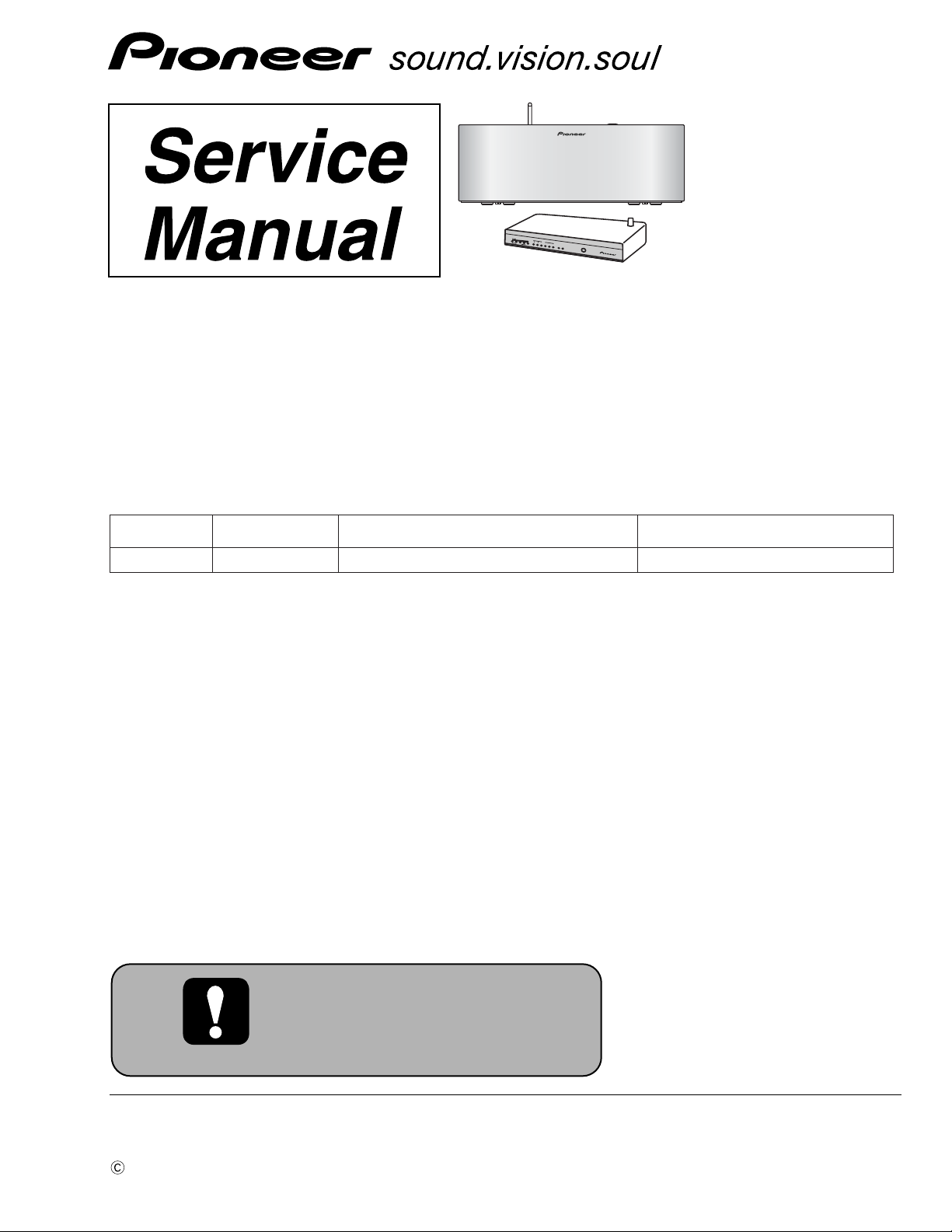
XW-HT1
Digital Wireless Speaker System
XW-HT1
THIS MANUAL IS APPLICABLE TO THE FOLLOWING MODEL(S) AND TYPE(S).
Model Type Power Requirement Remarks
XW-HT1
KUCXJ
AC120V
For details, refer to "Important symbols for good services" .
T-ZZR AUG. 2004 printed in Japan
Page 2
1234
SAFETY INFORMATION
A
This service manual is intended for qualified service technicians; it is not meant for the casual
do-it-yourselfer. Qualified technicians have the necessary test equipment and tools, and have been
trained to properly and safely repair complex products such as those covered by this manual.
Improperly performed repairs can adversely affect the safety and reliability of the product and may
void the warranty. If you are not qualified to perform the repair of this product properly and safely, you
should not risk trying to do so and refer the repair to a qualified service technician.
WARNING
This product contains and certain electrical parts contain chemicals which are known to the state of California to cause cancer,
B
birth defects or other reproductive harm.
Health & Safety Code Section 25249.6 – Proposition 65
NOTICE
(FOR CANADIAN MODEL ONLY)
Fuse symbols (fast operating fuse) and/or (slow operating fuse) on PCB indicate that replacement
parts must be of identical designation.
REMARQUE
(POUR MODÈLE CANADIEN SEULEMENT)
Les symboles de fusible (fusible de type rapide) et/ou (fusible de type lent) sur CCI indiquent que
C
les pièces de remplacement doivent avoir la même désignation.
(FOR USA MODEL ONLY)
1. SAFETY PRECAUTIONS
The following check should be performed for the
continued protection of the customer and service
technician.
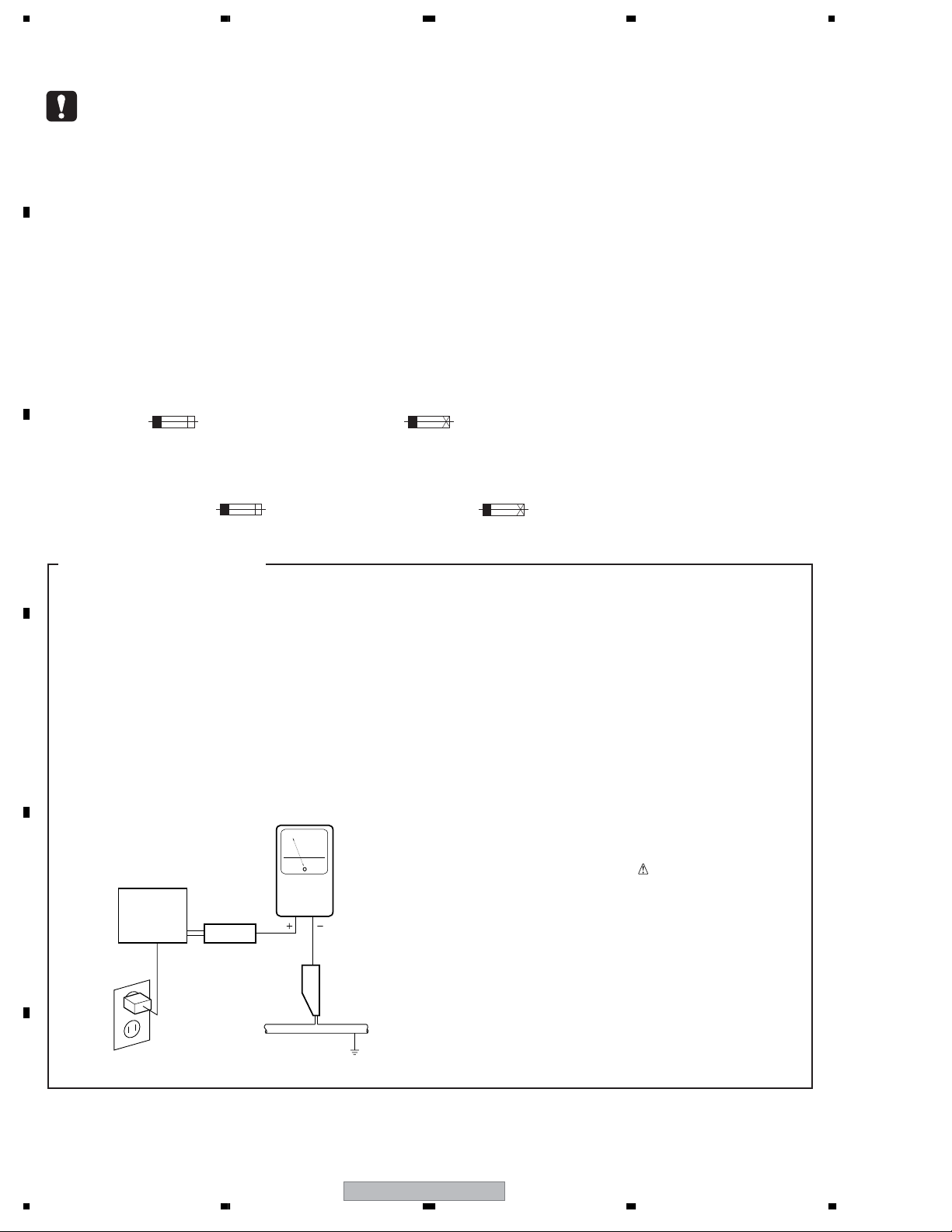
LEAKAGE CURRENT CHECK
Measure leakage current to a known earth ground
(water pipe, conduit, etc.) by connecting a leakage
current tester such as Simpson Model 229-2 or
D
equivalent between the earth ground and all exposed
metal parts of the appliance (input/output terminals,
screwheads, metal overlays, control shaft, etc.). Plug
the AC line cord of the appliance directly into a 120V
AC 60 Hz outlet and turn the AC power switch on. Any
current measured must not exceed 0.5 mA.
Leakage
current
E
Device
under
test
Also test with
plug reversed
(Using AC adapter
plug as required)
Test all
exposed metal
surfaces
AC Leakage Test
tester
Reading should
not be above
0.5 mA
Earth
ground
ANY MEASUREMENTS NOT WITHIN THE
LIMITS OUTLINED ABOVE ARE INDICATIVE
OF A POTENTIAL SHOCK HAZARD AND
MUST BE CORRECTED BEFORE RETURNING THE APPLIANCE TO THE CUSTOMER.
2. PRODUCT SAFETY NOTICE
Many electrical and mechanical parts in the appliance
have special safety related characteristics. These are
often not evident from visual inspection nor the
protection afforded by them necessarily can be obtained
by using replacement components rated for voltage,
wattage, etc. Replacement parts which have these
special safety characteristics are identified in this
Service Manual.
Electrical components having such features are
identified by marking with a
on the parts list in this Service Manual.
The use of a substitute replacement component which
does not have the same safety characteristics as the
PIONEER recommended replacement one, shown in the
parts list in this Service Manual, may create shock, fire,
or other hazards.
Product Safety is continuously under review and new
instructions are issued from time to time. For the latest
information, always consult the current PIONEER
Service Manual. A subscription to, or additional copies
of, PIONEER Service Manual may be obtained at a
nominal charge from PIONEER.
on the schematics and
F
2
1234
XW-HT1
Page 3
5678
[Important Check Points for Good Servicing]
In this manual, procedures that must be performed during repairs are marked with the below symbol.
Please be sure to confirm and follow these procedures.
1. Product safety
Please conform to product regulations (such as safety and radiation regulations), and maintain a safe servicing environment by
following the safety instructions described in this manual.
1 Use specified parts for repair.
Use genuine parts. Be sure to use important parts for safety.
2 Do not perform modifications without proper instructions.
Please follow the specified safety methods when modification(addition/change of parts) is required due to interferences such as
radio/TV interference and foreign noise.
3 Make sure the soldering of repaired locations is properly performed.
When you solder while repairing, please be sure that there are no cold solder and other debris.
Soldering should be finished with the proper quantity. (Refer to the example)
4 Make sure the screws are tightly fastened.
Please be sure that all screws are fastened, and that there are no loose screws.
5 Make sure each connectors are correctly inserted.
Please be sure that all connectors are inserted, and that there are no imperfect insertion.
6 Make sure the wiring cables are set to their original state.
Please replace the wiring and cables to the original state after repairs.
In addition, be sure that there are no pinched wires, etc.
7 Make sure screws and soldering scraps do not remain inside the product.
Please check that neither solder debris nor screws remain inside the product.
8 There should be no semi-broken wires, scratches, melting, etc. on the coating of the power cord.
Damaged power cords may lead to fire accidents, so please be sure that there are no damages.
If you find a damaged power cord, please exchange it with a suitable one.
9 There should be no spark traces or similar marks on the power plug.
When spark traces or similar marks are found on the power supply plug, please check the connection and advise on secure
connections and suitable usage. Please exchange the power cord if necessary.
0 Safe environment should be secured during servicing.
When you perform repairs, please pay attention to static electricity, furniture, household articles, etc. in order to prevent injuries.
Please pay attention to your surroundings and repair safely.
A
B
C
D
2. Adjustments
To keep the original performance of the products, optimum adjustments and confirmation of characteristics within specification.
Adjustments should be performed in accordance with the procedures/instructions described in this manual.
3. Lubricants, Glues, and Replacement parts
Use grease and adhesives that are equal to the specified substance.
Make sure the proper amount is applied.
4. Cleaning
For parts that require cleaning, such as optical pickups, tape deck heads, lenses and mirrors used in projection monitors, proper
cleaning should be performed to restore their performances.
5. Shipping mode and Shipping screws
To protect products from damages or failures during transit, the shipping mode should be set or the shipping screws should be
installed before shipment. Please be sure to follow this method especially if it is specified in this manual.
56
XW-HT1
E
F
3
7
8
Page 4

1234
CONTENTS
SAFETY INFORMATION..................................................................................................................................... 2
1. SPECIFICATIONS ............................................................................................................................................ 5
2. EXPLODED VIEWS AND PARTS LIST ............................................................................................................ 6
A
B
C
D
2.1 PACKING SECTION .................................................................................................................................. 6
2.2 TRANSMITTER SECTION......................................................................................................................... 8
2.3 WIRELESS SPEAKER SECTION........................................................................................................... 10
3. BLOCK DIAGRAM AND SCHEMATIC DIAGRAM ..........................................................................................12
3.1 BLOCK DIAGRAM ................................................................................................................................... 12
3.2 OVERALL WIRING DIAGRAM................................................................................................................. 14
3.3 DSP(1/2) and DSP-LED ASSYS.............................................................................................................. 16
3.4 DSP(2/2) ASSY........................................................................................................................................ 18
3.5 AMP, PRIMARY, BINDER and LED ASSYS............................................................................................. 20
3.6 TX MODULE(1/3) ..................................................................................................................................... 22
3.7 TX MODULE(2/3) ..................................................................................................................................... 24
3.8 TX MODULE(3/3) ..................................................................................................................................... 26
3.9 RX MODULE(1/4) .................................................................................................................................... 28
3.10 RX MODULE(2/4) .................................................................................................................................. 30
3.11 RX MODULE(3/4) .................................................................................................................................. 32
3.12 RX MODULE(4/4) .................................................................................................................................. 34
3.13 WAVEFORMS........................................................................................................................................ 36
4. PCB CONNECTION DIAGRAM ..................................................................................................................... 37
4.1 DSP ASSY ............................................................................................................................................... 38
4.2 DSP-LED ASSY....................................................................................................................................... 40
4.3 AMP and BINDER ASSY ......................................................................................................................... 42
4.4 PRIMARY and AMP-LED ASSYS............................................................................................................ 44
4.5 TX MODULE ............................................................................................................................................ 46
4.6 RX MODULE............................................................................................................................................ 48
5. PCB PARTS LIST ........................................................................................................................................... 50
6. ADJUSTMENT ............................................................................................................................................... 53
7. GENERAL INFORMATION ............................................................................................................................. 54
7.1 DIAGNOSIS ............................................................................................................................................. 54
7.1.1 DIAGNOSIS NOTE ............................................................................................................................. 54
7.1.2 TROUBLESHOOTING........................................................................................................................ 55
7.1.3 POWER ON SEQUENCE................................................................................................................... 57
7.1.4 NOTES ON REPLACE OF PARTS ..................................................................................................... 58
7.1.5 DIAGNOSIS OF THE AMPLIFIER SECTION..................................................................................... 58
7.1.6 PROTECTION CIRCUIT..................................................................................................................... 59
7.1.7 DISASSEMBLY ................................................................................................................................... 60
7.1.8 The style of a wire rod........................................................................................................................ 62
7.2 IC ............................................................................................................................................................. 63
8. PANEL FACILITIES ........................................................................................................................................ 75
E
F
4
1234
XW-HT1
Page 5
5678
1. SPECIFICATIONS
Specifications
General
Digital Wireless Speaker System
(Transmitter/Wireless speaker)
Transmitter
AC adapter
Power requirements . . . . . . . . AC 120V, 60Hz
Rated output . . . . . . . . . . . . . . . . . 12V/500mA
Power consumption (without AC
adapter) . . . . . . . . . . . . . . . . . . . . . . . . . . . . . . 7W
Input . . . . . . . . . . . . . . . . . . . . . . . . . . . . RCA jack
Weight . . . . . . . . . . . . . . . . . . . . 0.6 kg / 1 lb 5 oz.
Dimensions . . . . 255(W) x 58.5(H) x 121(D) mm
10(W) x 2
Wireless speaker
Power requirements . . . . . . . . . . AC 120V, 60Hz
Power consumption . . . . . . . . . . . . . . . . . . . 26W
Amplifier characteristics
Maximum power output . . . . . . . . . . . . . 10W/ch
RMS (1kHz, THD10%, 4Ω)
Speaker unit. . . . . . . . . . . . . . . 7cm cone type x 2
Weight . . . . . . . . . . . . . . . . . . . 2.9 kg / 6 lbs 6 oz
Dimensions (without
antenna) . . . . . . 461.5(W) x 176.5(H) x 95(D) mm
3
18
Depth with antenna. . . . . . . . . 110 mm / 4
Accessoriess
Remote control . . . . . . . . . . . . . . . . . . . . . . . . . .1
Lithium battery (CR2025) . . . . . . . . . . . . . . . . . .1
AC adapter. . . . . . . . . . . . . . . . . . . . . . . . . . . . . .1
RCA/phono stereo audio cable . . . . . . . . . . . . .1
Power cord. . . . . . . . . . . . . . . . . . . . . . . . . . . . . .1
Radio wave caution sheet. . . . . . . . . . . . . . . . . . 1
Warranty card . . . . . . . . . . . . . . . . . . . . . . . . . . .1
These operating instructions
5/16(H) x 43/4(D)in.
/16(W) x 615/16(H) x 33/4(D)in.
. . . . . . . . . . . . . . . . . . . . . . . . . 1
5
/16 in.
Accessories
Checking the supplied
accessories
Please check that you've received the
following supplied accessories:
• Remote control unit
• Lithium battery (CR2025)
• RCA/phono stereo audio cable
VOLUME
SURROUND MODE
DVD
CS∏∏CINEMA CS MUSIC W.STEREO
W.STEREOTVMUSICCINEMA
INPUT ATTWIRELESS OFF
A
B
C
MUTE
D
Note
•
The specifications and design of this
product are subject to change without
notice, due to improvement.
XW-HT1
56
• Power cord
• AC adapter
• Operating instructions
• Radio wave caution sheet
• Warranty card
7
E
F
5
8
Page 6
1234
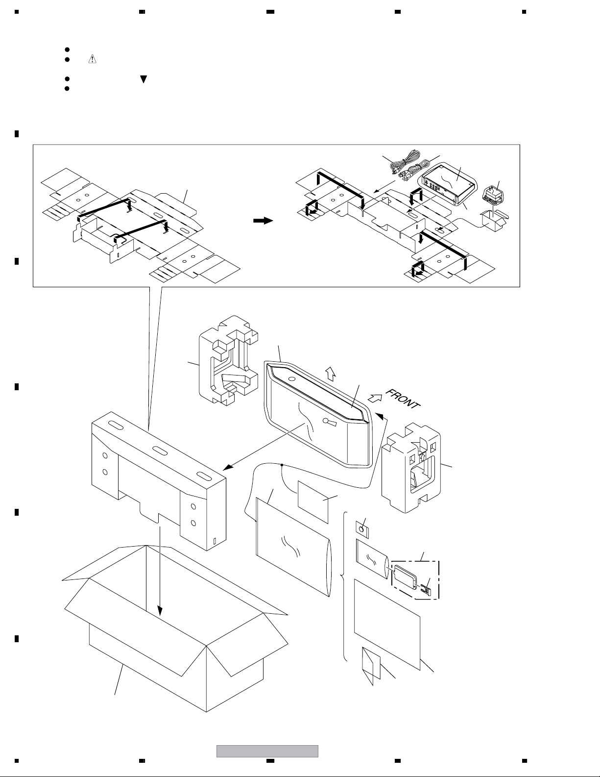
2. EXPLODED VIEWS AND PARTS LIST
NOTES:
Parts marked by "NSP" are generally unavailable because they are not in our Master Spare Parts List.
The mark found on some component parts indicates the importance of the safety factor of the part.
A
Therefore, when replacing, be sure to use parts of identical designation.
Screws adjacent to mark on product are used for disassembly.
For the applying amount of lubricants or glue, follow the instructions in this manual.
(In the case of no amount instructions, apply as you think it appropriate.)
2.1 PACKING SECTION
B
C
13
3
1
V
2
1
N
I
C
D
TV
D
V
D
TV
TRANSMITTER
2
12
12
14
TOP
WIRELESS SPEAKER
D
14
11
7
6
4
E
5
9
F
6
15
XW-HT1
8
1234
Page 7

>
5678
PACKING SECTION parts List
No. Description Part No.
Mark
1AC Power Cord ADG7021
2AC Adapter AWR7019
3 RCA Stereo Cord XDE3045
4 Remote control unit AXD7402
5 Battery Cover AZN7998
NSP 6 Lithium Battery (CR2025) VEM1009
7 2.4GHz Caution Sheet ARM7088
8 Operating Instructions ARE7351
(English, French)
9Warranty Card (PA/POC) ARY7045
10 • • • •
NSP 11 Polyethylene Bag Z21-038
(0.03x230x340)
12 Packing Sheet (large) AHG7015
NSP 13 ACCESSORY BOX AHB7094
14 Pad L/R AHA7440
15 Packing Case AHD8297
16 • • • •
A
B
C
D
E
56
XW-HT1
F
7
7
8
Page 8
1234
2.2 TRANSMITTER SECTION
A
B
9
2
10
NON-CONTACT
SIDE
CONTACT SIDE
C
D
E
∗1 : Since it is torque screw,
use a TORX driver.
B
12
(1/2)
8
8
(2/2)
12
1
A
3
G
4
7
12
12
12
12
12
∗1
11
F
8
1234
6
13
11
∗1
5
6
XW-HT1
Page 9

*
5678
TRANSMITTER SECTION parts List
No. Description Part No.
Mark
1 DSP Assy AWU8244
2 DSP-LED Assy AWU8245
3 TX Module AXF7010
4 19P Flexible Cable ADD7499
5 Chassis T ANA7172
6 Leg AEB7090
7 Radiation Sheet B AEB7237
8 MODE button AAD7737
9 Window AAK8265
10 Top Panel AAK8264
A
11 TORX Screw *
12 Screw BPZ30P080FTC
NSP 13 NAME LABEL T(PAP) AAL7370
Use TORX driver GGK1028.
ABA7111
B
C
D
56
XW-HT1
E
F
9
7
8
Page 10
1234
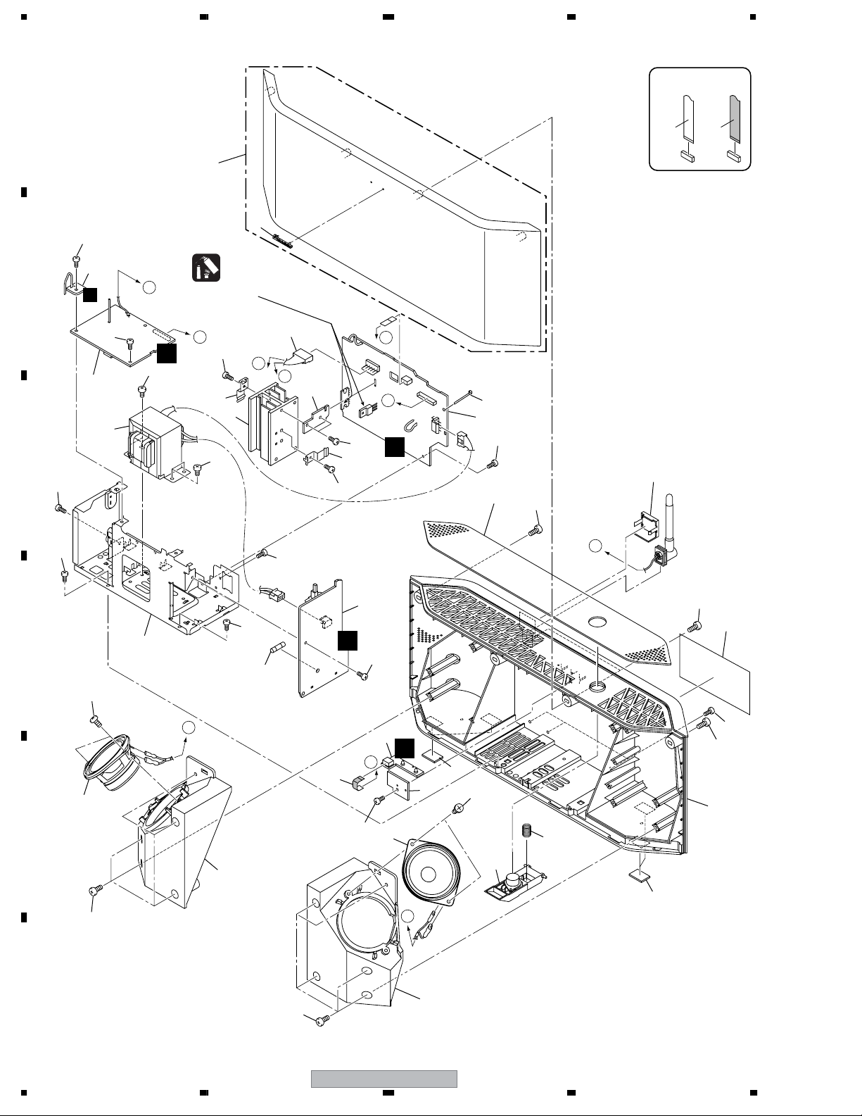
2.3 WIRELESS SPEAKER SECTION
A
22
23
32
4
B
F
32
A
H
5
C
32
33
31
6
Lubricating Oil
GYA-009
B
32
12
13
31
35
9
C
D
26
32
32
12
32
E
B
C
16
1
32
18
34
A
NON-CONTACT
17
SIDE
CONTACT SIDE
3
33
D
34
10
E
34
F
11
7
C
19
34
D
32
2
E
E
8
33
10
D
25
20
15
34
14
21
15
34
27
32
34
24
10
XW-HT1
1234
Page 11

>
>
5678
WIRELESS SPEAKER SECTION parts List
No. Description Part No.
Mark
1 AMP Assy AWU8246
2 AMP-LED Assy AWU8248
3 PRIMARY Assy AWU8247
4 BINDER Assy AWU8251
5 RX Module AXF7011
6Power Transformer ATS7388
7 Fuse (FU1 : 1.25A) REK1108
8 5P Flexible Cable ADD7498
9 4P Cabe Assy ADX7470
10 Speaker B70AC50-52C
A
11 Chassis ANA7176
12 FET Bracket A ANG7432
13 HEAT SINK (AL) ANH7178
14 SPRING K(MTL) ABH7239
15 RUBBER LEG AEB7353
NSP 16 BINDER(BK-1) ZCA-BK1
17 ANTENNA COVER(PLS) AAK8263
18 OPERATION PANEL AAK8260
19 Baffle L AMD7015
20 Baffle R AMD7016
21 PWR Button Assy AXG7245
22 Grille Assy AXG7240
23 NAME PLATE 36(PLS) AAM7013
24 Rear Case Assy AXG7241
NSP 25 ANGLE B
NSP 26 ANGLE A
NSP 27 NAME LABEL(KUC) AAL7369
28 • • • •
29 • • • •
30 • • • •
31 Screw BBZ40P060FTC
32 Screw BBZ30P080FNI
33 Screw BPZ30P080FTC
34 Screw BPZ40P100FNI
35 Lubricating Oil GYA-009
B
C
D
56
XW-HT1
E
F
11
7
8
Page 12
1234
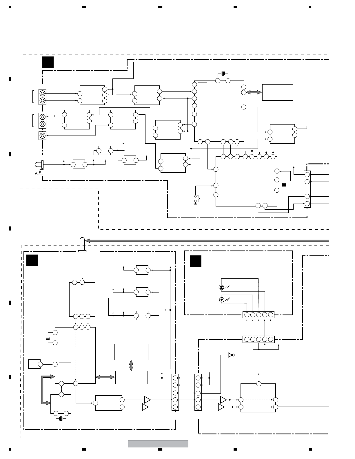
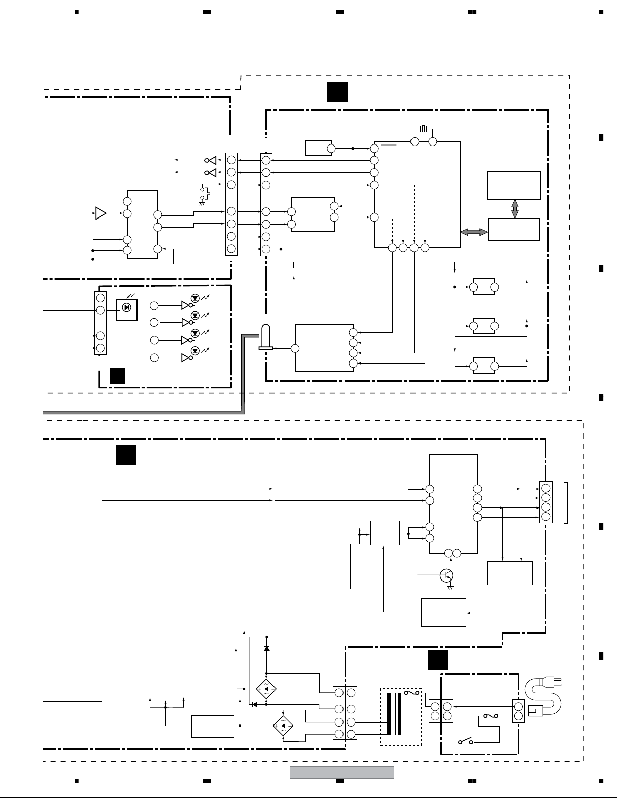
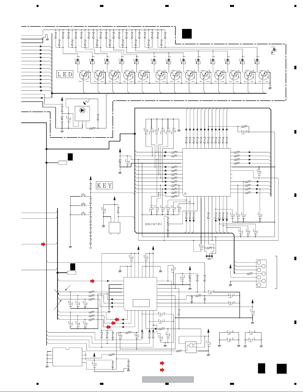
3. BLOCK DIAGRAM AND SCHEMATIC DIAGRAM
3.1 BLOCK DIAGRAM
A
TRANSMITTER SECTION
DSP ASSY
A
V+5A
V+5D
IC1503
IC1201
AK5357VT
AINL
2
AINR
1
5
3
V+2.5V
A / D
SDT0
MCLK
9
11
PCM1754
VoutL
7
VoutR
8
7
8
IC1601
D / A
DATA
IC1631
PCM1754
D / A
VoutL
VoutR
SCK
DATA
SCK
RESET
13
SDI0
25
MCK
30
31
BCKO
LRO
32
SDO0
3
2
16
2
16
KEY
IC1151
BU4052
1
IC1602
NJM2115M
OP AMP
5
BA09SFP
9V REG.
1 3
INPut Selector
X0
12
Y0
1
IC1501
InputB
9
InputA
10
X
13
3
7
IC1502
NJM78M05DL1A
5V REG.
1 3
1
IC1632
BU4558
OP AMP
7
1 3
NJM2391DL1-25
2.5V REG.
JA81131
L
R
INPUT
Analog Audio
B
L
R
Analog Audio
SW OUT
OUT PUT
JA1501
DC IN
12V
V LED V+9 VA+9SW
C
SDO1
SDOUT
5
X1301
36.864MHz
10 11
XI
X0
IC1301
NJU26150
DSP Chip
SDIN7SCK
10
SDIN
SDOUT
9
KEY1
3
XRRESET
2
SDO2
8
42
12
11
SCK
16
4
1
SSX
47
SSX
INPUTSELB
IC1401
PDC118A
CPU Chip
43
46
INPUTSELA
PDL019A8
EEPROM
2
16
44 45
SEVOLCLK
SRVOLDAT
VOL1
VOL2
2321
IC1303
Interface
IC1661
PCM1754
D / A
DATA
SCK
1
SRVOLCE
CF1
6
CF2
7
VoutL
VoutR
Vol. Control
V+5D
RCON
X1401
10MHz
7
8
RCON
CN1471
17
18
16
14
(19P)
RECEIVER SECTION
RX MODULE
D
E
F
H
X3
24.576MHz
U20
AIC1680
System Reset
3
VCXO1-VCXO8
3
5
7
NC7SPU04
VCXO
2 4
12.288MHz
1714
RFANT2
U16
AWD601RX
RF Rx Module
DATA6CHAN18CHAN4
11
40
35
31
CLKIN
RFINSDTI
CLKOUT
Freesystems Rx Chip
RESETIN
VCLKIN
54
6
U18
P5X
X2
U2
FS2105RX
58
CHANNEL3
ANT2
CHANNEL2
2
D/A Converter
A3V3
D5V
VOUTL
DATA
VOUTR
U28
PCM1742KE
U12
AIC1734-50CXA
5V REG.
D5V
2 3
U19
AIC1734-33CXA
3.3V REG.
D3V3
2 3
U17
NCP1117ST50T3
5V REG.
A5V
2 3
H6
52807-0910MOLEX
EEPROM Prog.
Interface
U11
EEPROM for FS
7
8
5
3
NJM4558
DAC Filter
RFSUPPLY+
+9V
+9V V+9RF
12
11
7
1
U24
10
CN3
(12P)
8
6
V+9
V+9
STATUS
LOUT
ROUT
AMP-LED ASSY
E
TUNED
POWER
CN5902
CN5901
Q5901
1
2
10
5
7
CN3701
(12P)
1
3
7
5
(5P)
(5P)
1 2 3 4
GNDO
1 2 3 4
X0
3
Y0
5
LEDP
LEDTUN2
VA+9
8
IC3301
BA4558
OP AMP
LEDTU1
X (Lch)
Y (Rch)
5
GNDD
5
VD+9
1
7
12
XW-HT1
1234
Page 13
5678
A
TX MODULE
G
BA4558F
V+5
RCON
VOL1
VOL2
IC1662
3
17
18
16
14
CN1472
(19P)
IC1751
LC75342M
LR Vol.
13
L2
1
GP1UM26XK
B
LOUT
14
L1
ROUT
1
DI
2
CE
IR1471
Other:Q1483-Q1488
DSP-LED ASSY
U3
AIC1680
System
CN1861
Q1865
Q1864
Ch. select
5
26
CL
30
Q1476
16
Q1480
14
Q1481
12
Q1482
15
Other:D1483,
D1471-D1478
(12P)
11
12
VOL 1
VOL 2
VOL 3
VOL 4
CN2
(12P)
LED 2
3
4
2
6
8
LED 1
CHSEL
LIN
RIN
V+9RF
V+9RF
3
4
2
6
8
11
12
ANT1
Power On Reset
PLD02
PLD01
CHANNELSEL
AINL
2
AINR
1
AK5380VT
A/D Converter
+9V
RFINANT
12
1
13
SDTO
9
U9
U23
AWD601TX
RF Tx Module
DATA
CHAN2
CHAN1
CHAN3
RESET
11
CHANNELBIT1
64
CHANNELBIT2
12
CHNNELSEL
8
SDTO
58
1
8
9
7
X1
24.576MHz
3 5
CLKIN CLKOUT
Freesystems
RFOUT
CHANNEL1
CHANNEL2
31 33 34 35
U1
FS2105TX
Tx Chip
CHANNEL3
AIC1734-50CXA
REG.
+9V
3 2
NCP1117ST50T3
5V REG.
3 2
AIC1734-33CXA
3.3V REG.
D5V
3 2
52806-0910
EEPROM Prog.
Interface
EEPROM for FS
U21
U6
U22
H10
B
U7
RFSUPPLY+
A5V
C
D3V3
AMP ASSY
C
V+9RF
VD+9
VA+9
IC15
REG9V
NJM78M09FA
VPRE9
INSIDE
SPEAKER
D
E
F
SP
PROTECT
Q3451 Q3452
AN1CN2
NEUTRAL
LIVE
FU1
CN3401
(5P)
2
1
5
L +
4
L -
1
R +
2
R-
AC IN
IC1301
LA4663
Power IC
L IN
4
R IN
2
VP(+B)
8
POWER
+B
RELAY
RY3301
+B
D13
POWER Supply
D11
D12
D17
CN11
MAIN
1
1
MAIN
2
2
3
3
4
4
T1
POWER
TRANSFORMER
VCC2
VCC1
7
5 6
Q3511
GND
RELAY
DRIVE
Q3455
Q3454 Q3453
PRIMARY ASSY
D
1
1
2
2
MUTE
9
11
14
12
Relay Control
S1
L +OUT
L –OUT
R +OUT
R –OUT
56
XW-HT1
13
7
8
Page 14
1234
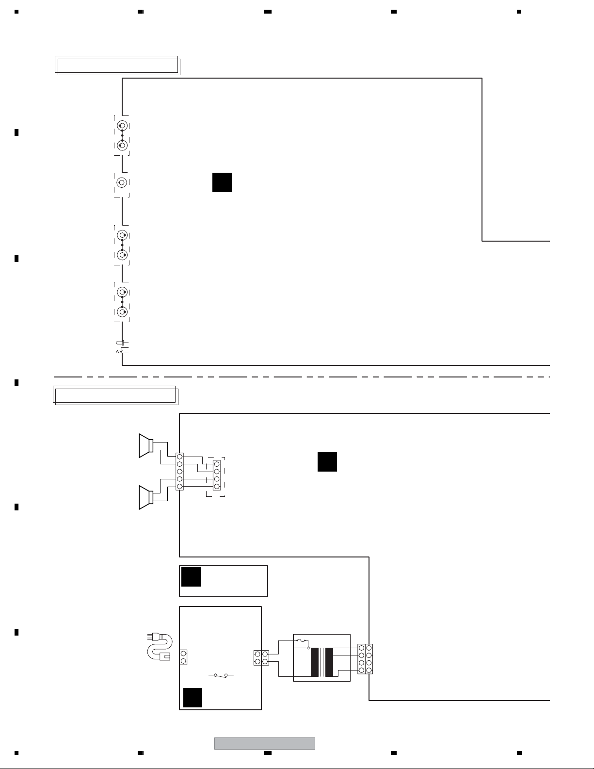
3.2 OVERALL WIRING DIAGRAM
A
B
• Transmitter Section
JA1801
BKB1017
TV
OUT
JA1831
VKB1159-
SW
OUT
L
L
R
SW
JA1101
DSP ASSY (AWU8244)
A
DVD
IN
R
BKB1017-
JA1131
L
TV
IN
DC12V
R
BKB1017-
JA1501
AKN7038-
1
3
IN
2
C
• Receiver Section
L ch
D
SPEAKER
: B70AC50-52C
R ch
SPEAKER
: B70AC50-52C
E
AC POWER CORD
: ADG7021
F
CN3401
B5P-VH
SR+ (L+)
5
SR- (L-)
44
NC
3
SL- (R-)
2
SL+ (R+)
11
TO SPEAKER
3
2
STBY
J3401
ADX7432-
BINDER ASSY
(AWU8251)
F
PCB BINDER : VEF1040
PRIMARY
ASSY
(AWU8247)
2
NEUTRAL
1
LIVE
XKP3041
AN1
S1
ASG7024-
AC POWER SW
D
CN2
B2P3-VH
1
1
22
C
AMP ASSY
(AWU8246)
T1
MAIN
1
MAIN
1
2
2
3
3
4
4
CN11
B4PS-VH
14
XW-HT1
1234
Page 15
5678
A
B
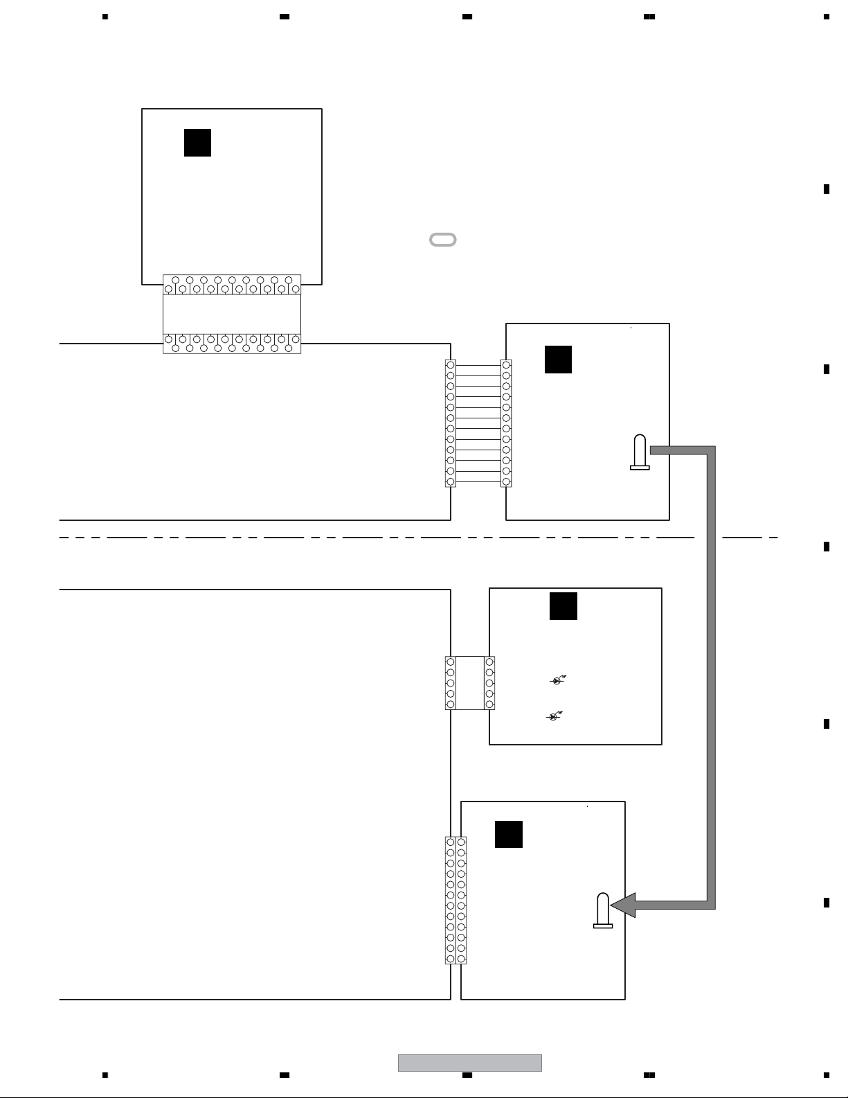
DSP-LED ASSY
(AWU8245)
CN1472
CKS3833-
4
32165
V+LED
GND_LED
GND_LED
1
2
CN1471
VKN1423- -TBB
TV_C
TV_M
543
TV_ST
CS2_ST
6
987
CS2_M
W_ OFF
987
10
11
ATTL
VOL3
CS2_C
111215
10
131215
VOL5
13
14
VOL2
14
VOL4
16
VOL1
16
17
V+5D
17
18
RMC
18
19
GNDSR
19
NOTES: • When ordering service parts, be sure to refer to “EXPLODED
VIEWS and PARTS LIST” or “PCB PARTS LIST”.
• The > mark found on some component parts indicates the
importance of the safety factor of the part.
Therefore, when replacing, be sure to use parts of identical
designation.
• : The power supply is shown with the marked box.
CN1861
12PL-FJ
1
2
3
4
5
6
7
8
9
10
11
12
STATUS
CHSEL
LED2
LED1
GNDA
LIN
GNDA
RIN
GNDRF
GNDRF
V+9RF
V+9RF
10
11
12
CN2
1
2
3
4
5
6
7
8
9
G
TX MODULE
(AXF7010)
ANT1
B
C
CN5901
52045-0545
CN3701
53290-1210
V+9
V+9
GND
GND
LOUT
GND(NC)
ROUT
GND
ERROR
STATUS
SCAN_MODE
(NC)
CH_SELECT
(NC)
CN5902
GNDD
11
LEDP
2
2
LEDTUN2
3
3
LEDTUN1
4
4
GNDD
5
5
52044-0545
CN3
1
212
363
4
5
6
77
8
99
11 11
121012
10
H
RX MODULE
4
5
(AXF7011)
8
E
AMP-LED ASSY
(AWU8248)
POWER
TUNED
ANT2
D
E
F
56
XW-HT1
15
7
8
Page 16
1234
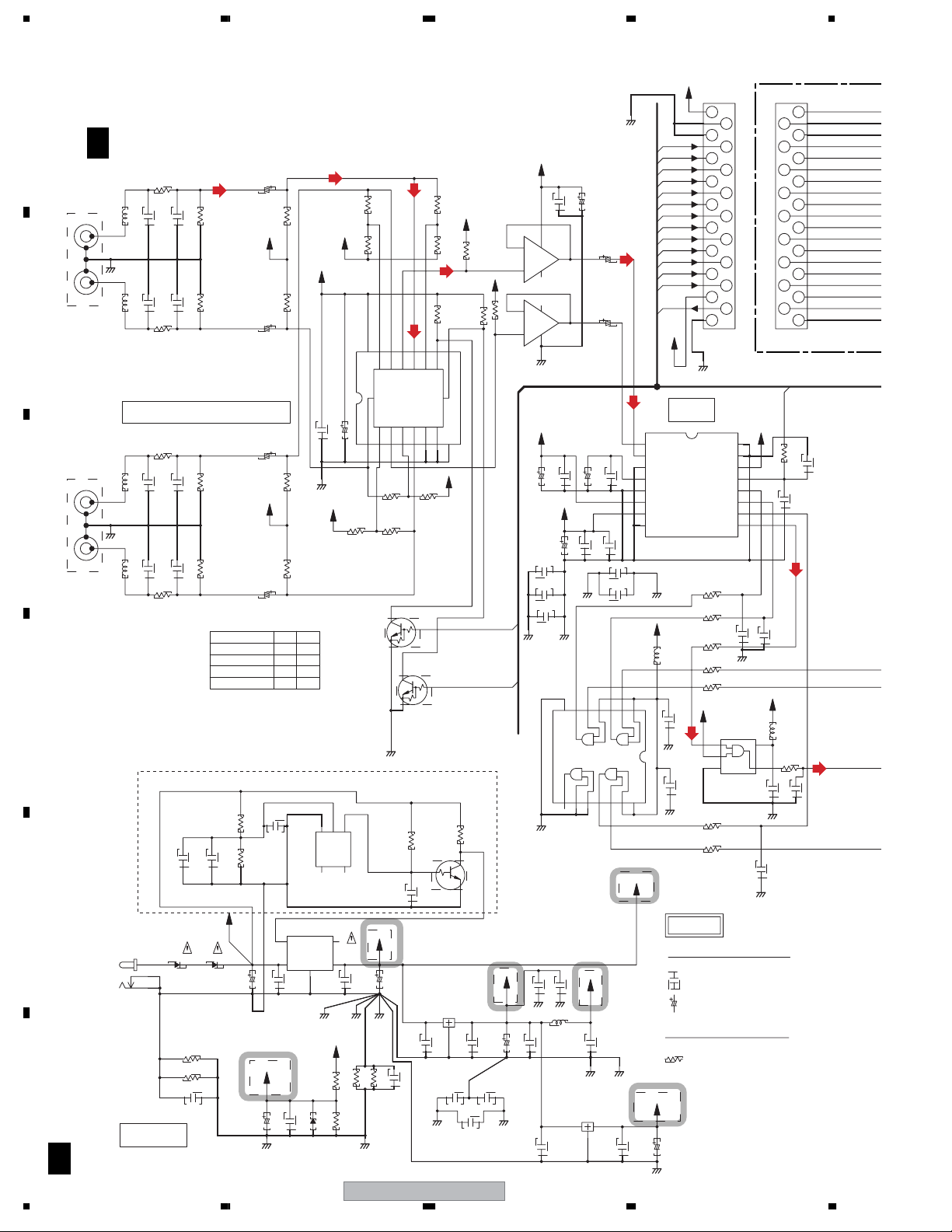
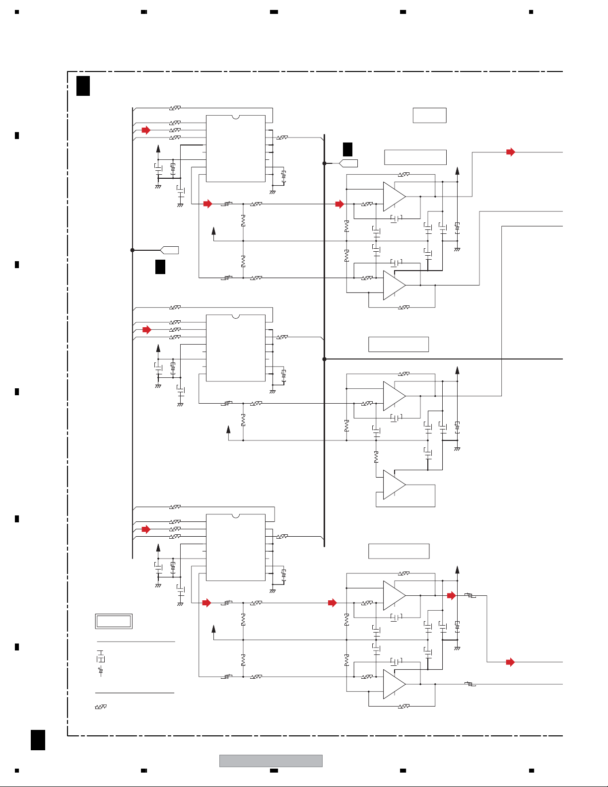
3.3 DSP(1/2) and DSP-LED ASSYS
V+LED
CN1471
A
GNDLED
A 1/2
DVD
JA1101
L
GNDA
B
C
R
BKB1017-
TV
JA1131
L
R
BKB1017-
GNDA
DSP ASSY(1/2) (AWU8244)
DVD
DVD
TV
TV
C1105
10/50
R1107
VC VC
R1108
C1106
10/50
C1135
10/50
R1137
VC
R1138
C1136
10/50
L
ATT
ON
H
ATT
LLH
ON
100K
100K
100K
100K
BA
L
HH
STBY
STBY
C1103
C1104
(A)
47p
R1103
47p
R1104
L1101
L1102
C1101
0Ω(R1191)
0Ω(R1192)
C1102
R1101
27K
R1102
27K
Input Selector
R1131
27K
0Ω(R1193)
STBY
C1131
C1132
R1132
27K
STBY
C1133
C1134
47p
R1133
47p
R1134
L1131
L1132
0Ω(R1194)
56K
56K
56K
56K
IC1151
Input Selector
(A)
V+9
C1152
C1151
0.01
GNDA
VC
DTC124EUA-TLB
(A)
27K
R1141
82K
R1142
1513141211109
X
X2
X1
OUT/IN
IC1151
Y0
BU4052BCF-TBB
10/50
R1144
82K
Y3Y2Y
OUT/IN
116
3247658
R1113 R1114
27K 82K
R1143
27K
Q1151
(A)
X0
Y1
27K
R1111
82K
R1112
(A)
47k
R1151
A
X3
B
VEE
INH
VC
Q1152
DTC124EUA-TLB
VC
100k
R1153
R1152
47k
INPUTSELA
INPUTSELB
R1154
Lch
VC
100K
Rch
V+9
C1155
2
8
-
3
+
4
6
8
-
5
+
4
IC1152
BA4558F-HT-TBB
GNDA
V+5A
C1201
10/50
V+5A
C1205
C1210
0.01
C1221
STBY
C1222
STBY
GNDD GNDA
0.01
1
7
C1202
10/50
47/25
C1156
IC1152
BA4558F-HT-TBB
(2/2)
2.2/50
C1203
0.1
0.1
C1206
GNDA
67435
C1153
10/50
C1154
10/50
C1204
C1226
BCK
(1/2)
(A)
C1223
0.01
C1227
0.01
D
TC74VHCT08AFT-TBB
8
912111013
Level Shift
2.5V–>5V
0.01
0.01
C1225
L1501
0Ω(R1591)
STBY
IC1503
NJM2391DL1-25-TLB
0.1
IC1202
LRCK
V+5D
STBY
C1514
GNDSR GNDM
C1509
Vout
C1503
1
NC
5
820
STBY
STBY
R1511
STBY
V+9
C1504
GND
R1512
GNDM
C1534
47/50
STBY
0.01
C1523
XW-HT1
27k
Q1511
R1533
DTC114TUA-TLB
0.01
IC1502
NJM78M05DL1A-TLB
0.1
C1511
0.01
C1522
GNDA
R1534
47k
C1507
STBY
C1525
STBY
0.01
C1521
V+5A
C1508
GNDD
GNDD
C1224
GND GNDA
47/50
C1513
C1512
Over input protection circuit
0.01
RS1/16S1003D-T
C1533
105 YB
STBY
R1513
STBY
R1514
STBY
C1524
C1532
V+LED
105 YB
R1532 R1531
RS1/16S5802D-T
IC1501
470/25
C1501
C1502
VC
470/6.3
C1505
C1506
GNDA GNDA
C1531
E
JA1501
AKN7038-
D1501 D1502
1SR154-400-TRB
1SR154-400-TRB
DC12V
F
Power
1/2
A
16
PST3242-TLB
BA09SFP
CTL NC
in
out
Gnd
0.1
GNDLED GNDRF
D1503
0.01
2
VDD
Vss
NC
43
IC1511
V+9
UDZS4.7B-TRB
R1501
R1502
TVC
TVM
CS2ST
TVST
CS2M
W_OFF
CS2C
ATTL
VOL3
VOL5
VOL2
VOL4
VOL1
RCON
V+5D
(A)
1
AINR
2
AINL
3
CKS1
4
VCOM
0.1
5
AGND
6
VA
AK5357VT-TBB
7
VD
8
DGND
STBY
GNDA
V+5A
0Ω(R1291)
MCK
L1201
2
1
C1208
GNDD
C1220
14
GNDD
V+9SW
UNLESS OTHERWISE SPECIFIED
ALL RESISTORS ARE IN
UNLESS OTHERWISE SPECIFIED
V+2_5V
C1510
470/6.3
STBY
GNDD
1
2
3
4
5
6
7
8
9
10
11
12
13
14
16
17 15
18
19
GNDSR
MICON
A/D
CKS0
CKS2
IC1201
NOTES
ALL CAPACITORS ARE IN
DIF
PDN
SCLK
MCLK
LRCK
SDTO
R1202
100
R1203
100
R1204
100
R1205
22
R1206
22
V+5A
(D)
1000p
IC1203
TC7SH08FU-TBB
15
2
34
Level Shift
0.01
5V–>2.5V
R1208
100
R1209
22
CKSRYB
AL :CEAL***M**-TS
NP :CEANP***M**-T
OTHER:CEAT***M##
RS1/16S***J-T
CKS3833-
VKN1423- -TBB
V+5A
16
15
14
13
12
11
10
9
CH
C1212
10p
C1213
GNDD
V+2_5V
C1218
GNDD
Ω
1
CN1472
C1207
10p CH
L1202
C1209
GNDD
CH
10p
uF
2
31
4
6
8
957
10
12
14
1513 1711
16
18
19
A/DPDOWN
100
R1201
C1526
0.01
(D)
0Ω(R1292)
(D)
R1207
C1217
0.0122STBY
STBY
1234
Page 17
5678
GNDLED
CS2ST
W_OFF
(D)
TVC
TVM
TVST
CS2M
CS2C
ATTL
VOL3
VOL5
VOL2
VOL4
VOL1
RCOM
GNDD
2.2kk
2.2kk
R1496
R1498
R1493
2.2kk
R1497
DISP
V+5D
47
R1460
47/10
C1452
C1451
AL
GNDSR
Switches
S1401 : VOL –
S1402 : VOL +
S1403 : MODE
VOL-
VOL+
DSP
MCK
MODE
BCK
SDI0
RESET
LRCK
SDI0
18.432MHz
MCK
3.072MHz
BCK
LRCK
SDO2
SDO1
48KHz
SDO0
SCK
SDIN
SSX
SDOUT
1
A0
2
A1
IC1303
3
A2
PDL019A8
EEPROM
4
GND
(M24C64-RMN6
+ White Dot Mark)
2.2kk
2.2kk
2.2kk
2.2kk
2.2kk
2.2kk
2.2kk
2.2kk
2.2kk
2.2kk
2.2kk
2.2kk
2.2kk
2.2kk
2.2kk
R1490
R1495
2.2kk
R1494
D1479
IR1471
GP1UM26XK
0.01
A 2/2
MB
VSG1024- -T
S1401
VSG1024- -T
S1402
VSG1024- -T
S1403
GNDM
A 2/2
DSP BUS
CH
10p
C1311
C1312
STBY
C1315
C1314
Vcc
WP
CLK
DATA
R1487
R1492
R1489
R1477
R1479
R1481
R1483
R1484
R1486
R1473
R1471
2.2kk
2.2kk
2.2kk
2.2kk
2.2kk
Q1483
B
VOL5
R1472
2.2kk
D1471
E
R1491
R1488
D1480
Q1479
DTC143EUA
-TLB -TLB -TLB -TLB -TLB -TLB -TLB -TLB -TLB -TLB -TLB -TLB -TLB
C
B
VOL1
D1481
Q1480
DTC143EUA DTC143EUA DTC143EUA DTC143EUA DTC143EUA DTC143EUA
E
C
EEC
B
VOL2
R1482
R1478
D1482
Q1481 Q1482
CCE
B
VOL3
R1485
D1483
B
VOL4
RCOM
Vcc
R1316
R1317
R1318
STBY
R1301
R1302
R1303
STBY
GND
C1313
C1316
8
7
6
5
TP
TP
TP
100K
Vout
R1453
R1452
100
V+5D
C1410
V+5D GNDM
R1454
10k
V+5D
1k
R1455
1.2k
0.1
C1453
R1456
GNDM
R1309
4
IC1451
PST3242-TLB
GNDD
4.7k
4.7k
R1310
R1319
100
Vss
NC
R1311
R1320
2315
VDDNCVout
SDI0
SDI1
SDI2
LRI
BCKI
MCK
BCKO
LRO
(D)
4.7k
4.7k
(D)
R1457
R1458
R1459
STBY
STBY
1.5k
1.8k
2.7k
C1310
22
22
22
22
22
22
V+2_5V
0.1
STBY
STBY
C1426
C1420
SWMUTE
0.01
C1409
XRESET
0.1
C1308
VSSR
VDDR
VSSR
24 23 22 21 20 1819
NJU26150-K
DSP
XSYSMUTE
A/DPDOWN
XWMUTE
SRVOLDAT
SRVOLCLK
SRVOLCE
INPUTSELA
INPUTSELB
STANDBYKEY1
V+2_5V
VDDR
VSSC
IC1301
C1307
VSSC
0.1
VDDC
STBY
C1419
VDDC
10/50
100K
R1451
GNDD GNDD
25
26
27
28
29
30
31
32
12 435768
(D)
SDO2
SDO0
SDO1
100
R1304
R1321
STBY
C1351
GPIO0
47p
SCL/SCK
SDA/SDOUT
100
R1305
AD2/SSX
AD1/SDIN
100
R1306
R1307
(D)
C1318
STBY
GNDD
2.2kk
R1474
R1476
2.2kk
R1475
D1472
Q1471
Q1472
CCE
B
B
CS2C
CS2M
STBY
STBY
STBY
STBY
C1422
STBY
C1401
C1423
100
100
100
100
100
100
100
100
100
100
10k
100p
R1445 R1446
R1436
VDD3
Vss3
R1431
R1442
R1433
R1434
R1435
R1437
R1438
R1430
R1447
C1402
STBY 10K
GNDM
C1424
R1432
0.01
C1403
C1421
C1425
STBY
C1411
R1401-R1408 : 100*8
V+2_5V
470p
17
100
C1352
GPIO1
16
VSCC
15
VDDC
14
RESETX
13
VSSO
12
XO
11
XI
10
VDDO
9
(A)
(D)
C1319
STBY
C1320
STBY
R1308
100
C1321
GNDM
R1323
STBY
C1317
STBY
R1312
100
: ANALOG SIGNAL ROUTE (L ch)
: DIGITAL SIGNAL ROUTE
DSP-LED ASSY (AWU8245)
B
D1473
D1474
Q1474 Q1475
E
C
B
TVC
TVC
FLASHDO
FLASHCLK
FLASHE/D
100
100
100
100
R1426
R1422
R1423
R1424
312930
D1475
Q1473
DTC143EUA DTC143EUA DTC143EUA DTC143EUA DTC143EUA DTC143EUA
E
C
B
CS2ST
TVST
TVM
CS2ST
100
100
100
R1428
R1427
R1429
36
343533
IC1401
u-COM
PDC118A-K
48 47 46 4445 43 42 41 40 38 3739
23164
5
CF1
CF2
TEST
0.01
R1401
RCON
V+2_5V
0.1
C1306
4.7k
Level Shift
2.5V–>5V
TC7SET08FU-TLB
5
4
Vss1
R1403
R1402
XRESET
C1305
10/50
GNDD 0.01
R1313
IC1302
KEY1
R1314
6.8K
R1315
680
1
2
3
C1404
47k
36.864MHz
R1404
R1440
0.01
STBY
220
R1322
C1304
VSS1085- - T
X1301
V+5D
C1309
GNDD
E
C
CS2M
100
R1425
R1420
897
VDD1
R1405
ASS7034- -T
10M
0.01
D1476
E
C
B
TVM
W_OFF
CS2C
VOL3
ATTL
100
100
100
100
R1419
R1417
R1418
25
26
273228
10
12
11
SSX
SCK
SDIN
SDOUT
R1406
R1408
R1407
SDOUT
SDIN
SCK
SSX
X1401
V+5D
GNDM
C1303
C1302
C1333 C1331
C1334 C1332
GNDD
Q1476
B
TVST
R1416
R1415
R1414
R1413
2120 22 23 24
Vss2
VDD2
PWM0
PWM1
13 14 15 16 17 18 19
STBY
C1405
7P
CH
7P
CH
STBY
0.01 0.01
XW-HT1
56
7
D1477
EEC
R1439
C1427
100
100
100
100
R1412
R1411
R1410
R1409
STBY
C1406
C1407
STBY
C1412
FLASHE/D
FLASHDO
FLASHCLK
XRESET
GNDM
GNDD
D1483,D1477
SLR-343VC(NPQ)-TS
other
SLR-343MC(NPQ)-TS
D1478
Q1477 Q1478
C
B
W_OFF
15k
STBY
VOL5
VOL2
VOL4
VOL1
C1408
CHIN2
100
CHIN1
100
DACMUTE
100
100
STBY
C1415
STBY
STBY
C1413
C1414
CN1401
1
3
R1441
220
5
7
V+2_5V
0.1
C1301
GNDD
0.01
GNDD
A
B
ATTL
0.01
RESET
STBY
STBY
2
4
6
1/2
8
E
GNDLED
WEN/DI
WDO
WCLK
RST
Vcc
Vss
NC
A
LED
X2
X11
B
C
D
For Flash
E
F
B
17
Page 18
1234
3.4 DSP(2/2) ASSY
A
A 2/2
MCK :
18.432MHz
BCK :
3.072MHz
LRCK :
48KHz
B
DSP BUS
C
D
E
NOTES
ALL CAPACITORS ARE IN
UNLESS OTHERWISE SPECIFIED
CKSRYB
AL :CEAL***M**-TS
NP :CEANP***M**-T
OTHER:CEAT***M##
ALL RESISTORS ARE IN
UNLESS OTHERWISE SPECIFIED
F
RS1/16S***J-T
DSP(2/2) ASSY (AWU8244)
R1601
MCK
22
R1602
(D)
(D)
(D)
BCK
SDO0
LRCK
V+5A
GNDA
MCK
BCK
SDO1
LRCK
V+5A
GNDA
MCK
BCK
SDO2
LRCK
V+5A
GNDA
R1603
R1604
C1602
C1601
0.01
DSP BUS
A 1/2
R1631
22
R1632
R1633
R1634
C1632
C1631
0.01
C1662
0.01
C1661
uF
Ω
10/50
C1604
GNDD
10/50
C1634
GNDD
22
10/50
C1664
GNDD
22
22
22
22
22
22
R1661
R1662
R1663
R1664
1
BCK
2
DATA
3
LRCK
4
IC1601
DGND
PCM1754
5
DBQ-TBB
NC
6
Vcc
7
VoutL
8
VoutR
0.01
(A)
C1605
10/50
VC
C1606
10/50
1
BCK
2
DATA
3
LRCK
4
IC1631
DGND
PCM1754
5
DBQ-TBB
NC
6
Vcc
7
VoutL
8
VoutR
0.01
22
22
22
0.01
1
2
3
4
5
6
7
8
BCK
DATA
LRCK
DGND
NC
Vcc
VoutL
VoutR
VC
C1635
10/50
VC
IC1661
PCM1754
DBQ-TBB
C1665
10/50
C1666
10/50
16
SCK
15
FMT
14
MUTE
13
DENP
12
TEST
11
ZEROA
10
Vcom
9
AGND
R1609
1.5k 1.5k
100k 100k
R1608 R1607
R1610 R1614
1.5k 1.5k
16
SCK
15
FMT
14
MUTE
13
DENP
12
TEST
11
ZEROA
10
Vcom
9
AGND
R1639
1.5k
100k
R1637
16
SCK
15
FMT
14
MUTE
13
DENP
12
TEST
11
ZEROA
10
Vcom
9
AGND
R1669
1.5k
100k
R1667
100k
R1668
R1670
1.5k
(I2S FORMAT)
R1605
0
(DEMP:OFF)
C1603
GNDA
(I2S FORMAT)
R1635
0
(DEMP:OFF)
C1633
GNDA
(I2S FORMAT)
R1665
0
(DEMP:OFF)
C1663
GNDA
10/50
10/50
10/50
DACMUTE
DACMUTE
DACMUTE
(A)(A)
(A)
A 1/2
MB
R1611
R1612
3.9k3.9k
R1641
3.9k
R1671
3.9k
R1672
3.9k
Front OUT
2
-
R1613
3
+
C1609
1500p
C1607
2200p
2200p
C1608
C1610
+
5
-
6
SW OUT
6
-
R1643
5
+
1.5k
C1639
0.047
0.047
C1637
R1647
100k
+
3
-
2
Rear OUT
2
-
R1673
3
+
1.5k
C1669
1500p
1500p
C1667
1500p
C1668
C1670
1500p
R1674
+
5
1.5k
-
6
R1615
4.7k
IC1602
8
NJM2115M-TFB
1
4
1500p
4
7
IC1602
NJM2115M-TFB
8
R1616
4.7k
R1645
3.9k
IC1632
8
BA4558F-HT
7
4
4
1
IC1632
BA4558F-HT
8
R1675
1.5k
IC1662
8
BA4558F-HT
1
4
4
7
IC1662
BA4558F-HT
8
R1676
1.5k
D/A
(1/2)
C1612 C1611
(1/2)
(1/2)
-TBB
C1642 C1641
(2/2)
-TBB
(1/2)
-TBB
C1671
C1672
(2/2)
-TBB
0.01
0.01
MICON
0.01
0.01
0.01
0.01
C1613
C1643
C1673
(A)
V+9
10/50
C1614
0.01
GNDA
V+9
10/50
C1644
0.01
GNDA
V+9
(A)
C1675
10/50
10/50
C1674
0.01
GNDA
C1676
10/50
(A)
18
A
2/2
XW-HT1
1234
Page 19
5678
A
: The power supply is shown with the marked box.
Q1801
(A) (A) (A) (A)
C1801
10/50
C1802
10/50
C1831
10/50
100k
R1801
100k
R1802
100k
R1831
Q1803
DTA143EUA
DTC114TUA
Q1804
-TLB
V+9
1SS355-TRB
1SS355-TRB
2SD2114K
10k
R1809
Q1805
DTC124EUA
D1801
D1802
D1831
1SS355
-TRB
DTA143EUA
DTC114TUA
2SD2114K
(VW)-TLB
R1803
510
R1805
4.7k
R1806
4.7k
R1804
510
(VW)-TLB
R1833
510
R1835
4.7k
Q1831
(VW)-TLB
Q1833
Q1834
-TLB -TLB
Q1802
2SD2114K
V+9
C1835
C1836
R1837
C1837
10k
R1839
Q1835
DTC124EUA
R1807
1k
STBY
STBY
R1808
1k
STBY
1k
C1803
C1804
C1833
1000p
1000p
0.01
GNDA
L1801
0Ω(R1901)
L1802
0Ω(R1902)
L1831
0Ω(R1903)
GNDA
JA1801
BKB1017
JA1831
VKB1159-
SW
L
TV OUT
R
SW OUT
B
C
SRVOLCE
SRVOLDAT
220
220
R1751
R1752
(A)
IC1751
LC75342M-TBB
1
DI
STBY
STBY
C1758
C1757
C1759
C1760
GNDM
(A)
GNDA GNDA
229
STBY
CE
3
VSS
427
TEST
5
STBY
LOUT
625
GNDA
LBASS2
724
LBASS1
8
C1751
LTRE
922
LIN
10/50
10
LSELO
11
L4
12
L3
13
L2
14 17
L1
15
NC
+VOL
VDD
VREF
ROUT
RBASS2
RBASS1
RTRE
RSELO
XSYSMUTE
GNDM
SRVOLCLK
XWMUTE
Switches
Q1866
DTA143EUA
Q1867
DTC114TUA
(DVD,TV)
-TLB
-TLB
C1861
10/50
C1862
10/50
S1861 : Ch. select
CH Select
SW.
CH
Select
GNDD
R1863
510
D1861
R1865
100k
1SS355
-TRB
D1862
1SS355
100k
-TRB
Input
Terminal
L2,R2
L1,R1
4.7k
R1866
4.7k
R1864
510
R1861
R1862
V+9
10k
R1869
Q1868
DTC124EUA
220
R1753
30
CL
100/25
C1756
28
NC
26
23
C1752
RIN
10/50
21
20
R4
19
R3
18
R2
R1
16
NC
C1755
0.01
GNDM
V+9
10/50
0.01
C1754
C1753
GNDA
MODE
CS2
Cinema,Cinema
CS2
Music ,Music
W-Stereo
(D)
: DIGITAL SIGNAL ROUTE
(A)
: ANALOG SIGNAL ROUTE (L ch)
GNDM
CHIN1
V+5D
47k
R1810
Q1864 Q1865
DTC124EUA DTC124EUA
-TLB -TLB
SW1861
VSG1024- -T
C1863
0.01
Q1861
2SD2114K
R1867
(VW)-TLB
STBY
C1865
C1868
STBY
R1868
Q1862
2SD2114K
(VW)-TLB
R1840
GNDA
470
470
V+9SW
: AUDIO SIGNAL ROUTE (Other Stereo Mode)
(A)(A)(A)
C1867
C1866
CHIN2
47k
1500p
1500p
R1896
0
R1891
0
R1894
R1895
SWMUTE
STBY
R1892
0
R1893
GNDRF
CN1861
12PL-FJ
STBY
10
0
C1891
STBY
11
12
1
STATUS
2
CHSEL
3
LED2
4
LED1
GNDA
5
LIN
6
GNDA
7
RIN
8
GNDRF
9
GNDRF
V+9RF
V+9RF
TO RF MODULE
D
H2
F 2/3
E
F
56
XW-HT1
A
2/2
19
7
8
Page 20
1234
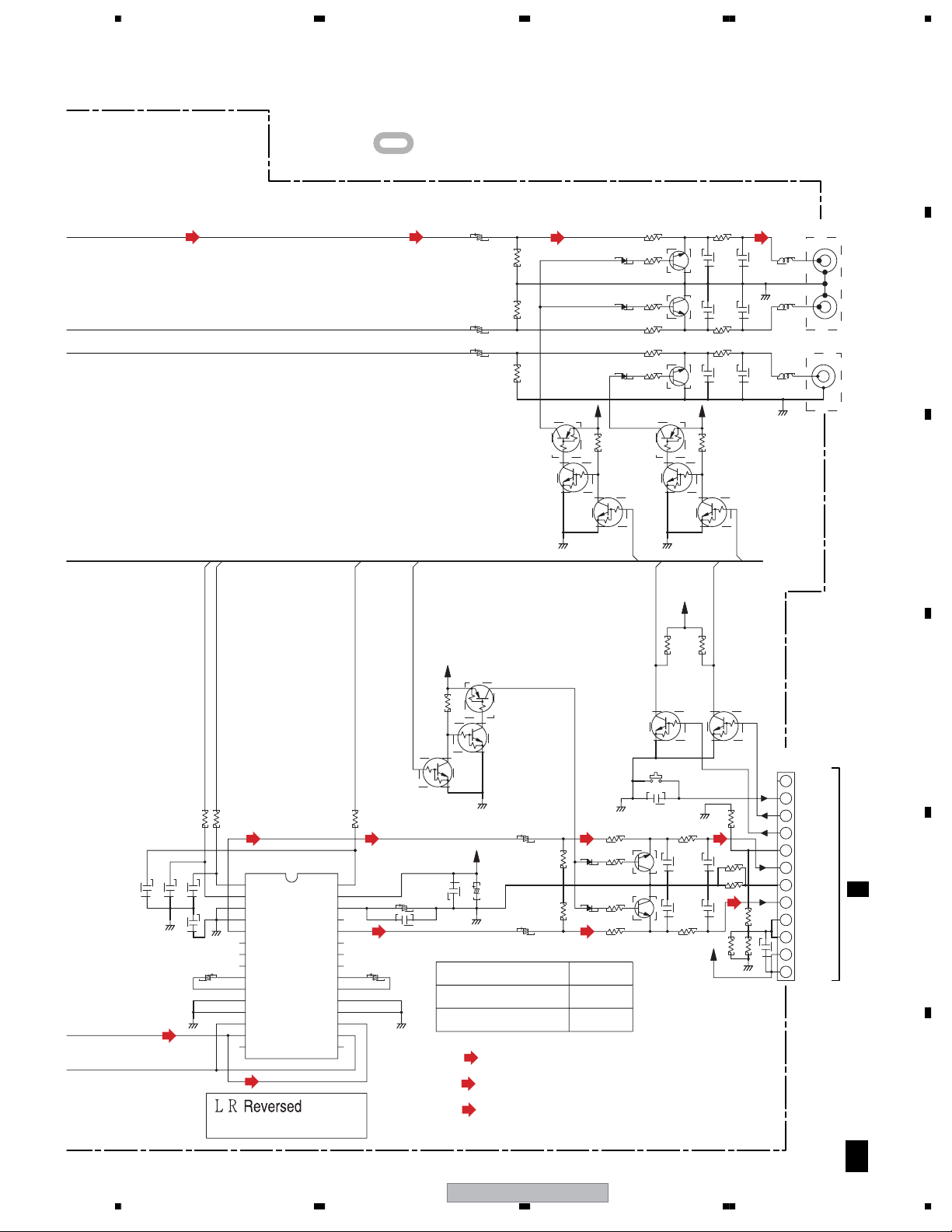
3.5 AMP, PRIMARY, BINDER and LED ASSYS
A
AMP ASSY
C
(AWU8249)
CN3401
B5P-VH
SR+ (L+)
5
SR- (L-)
4
3
NC
SL- (R-)
SL+ (R+)
LIVE
XKP3042
AN1
2
1
2
1
STBY
R3405
GNDP
CHASSIS
GND
BINDER ASSY
F
(AWU8251)
AKR7001- -T
H1
H2
FU1
0.01u
FU1 : REK1108
1.25A/125V
C3402
C3406
C3405
STBY
STBY
STBY
R3406
STBY
D3452 D3451
Q3454
2SC2412K(QR)
PCB BINDER : VEF1040
POWER TRANSFORMER
C1
STBY
S1
ASG7024-
C3
ACG7034-
STBY
(1/2)
RY3301
43
C
E
T1
ATS7388
W101
W102
W103
W104
C3401
ASR7019
B
R3463
B2P3-VH
CN2
L1
STBY
SP PROTECT
STBY
Q3451
2SA1576A
(QR)
B
10k
R3456
VPRE9
Q3455
2SD1858X(QR)
E
C
B
R3464
C3463
C3464
220/6.3
MAIN
MAIN
1
1
47/25
-TS
2
2
56k
C2
STBY
Q3452
2SA1576A
CC
B
EE
VREF5 VD+9
STBY
R3462
R3461
R3465
R3460
220220
220
C
E
D3453
UDZS9R1(B)
CN11
B4PS-VH
1
1
2
2
3
3
4
4
CAUTION
FOR CONTINUED PROTECTION AGAINST RISK OF FIRE,
REPLACE ONLY WITH SAME TYPE NO.491005 FOR
IC12 AND IC13, NO.49102.5 FOR IC11 AND IC14,
MFD. BY LITTELFUSE INC.
• NOTE FOR FUSE REPLACEMENT
CAUTION
B
C
D
E
F
TO SPEAKER
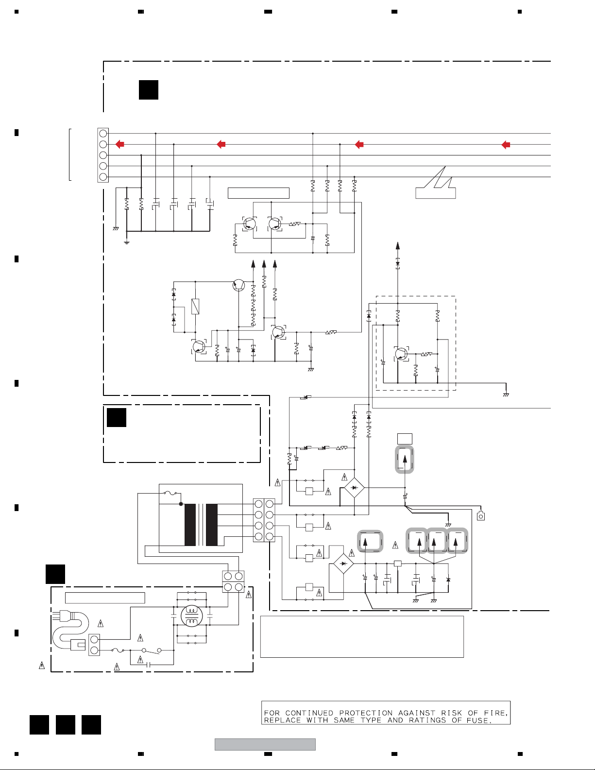
PRIMARY ASSY (AWU8247)
D
PRIMARY ASSY
AC CORD
NEUTRAL
POWER CORD
ADG7021
(QR)
R3457
10k
3.9k
Q3453
2SC4081
B
R3459
R15
1k
W109
IC13
IC14
AEK7049- -F
IC11
AEK7049- -F
W110
R3451
4.7k
NP
C3451
100/10
(QR)
10k
C3462
220/6.3
GNDD
D14
D15
D16
C15
10/50
W107
STBY
7A
IC12
AEK7047- -F
STBY
7A
AEK7047- -F
W108
STBY
2.5A
2.5A
STBY
R3452
4.7k
R3453
4.7k
R3455
R3458
10k
R16
1
D3SBA20(B)
D17
S1WB(A)60SD
~
-
~
4.7k
D12
D11
-
-TRB
+
R3454
R11
~
~
C16
4.7k
D13
1k
R12
+
VPRE9
2200/25
D3511
1k
C12
+B
D3503
POWER_ON MUTE
15k
R3511
Q3511
2SC4081(QR)
C
B
1/50
E
C3512
+B
+B
C13
6800/25
V+9RF VD+9
IC15
NJM78M09FA
-TS
STBY
1/50
C18
C17
GNDRF GNDD
R3514
R3513
6.8V
56k
56k
STBY
C19
R3512
C3511
GNDP
-TS
100/25
390k
47/25
D19
VA+9
STBY
GNDD
KN11
VNF1084-
CHASSIS GND
C D F
20
XW-HT1
1234
Page 21
5678
AMP ASSY
Lch
6.8 V
+B
RY3301
ASR7019
(2/2)
12
C3383
-TS
2.2/50
R3391
0
VP
R3315
STBY
IC3302 LA4663
R- OUT
R+ OUT
L- OUT
L+ OUT
GNDP
GNDP
12
10
14
C3355
C3356
R3352
IC3302
0.22
0.22
2.2
R3395
3.3k
LA4663
C3357
C3358
R3354
R3393
13
11
0.22
0.22
C3359
0.22
0.22
C3360
2.2
2.2
R3356
-TS
C3301
0.47/50
R3319
STBY
1k
SR+ (L+)
SR- (L-)
SL- (R-)
SL+ (R+)
100/25
C3310
C3311
0.01
0
R3312
10k
GNDP
R3313
10k
D3304
UDZS4R7(B)
B
Q3305
DTC114YK
R3399
820
C3308
AL-TS
C
E
STBY
GNDP
C3306
10/50
C3351
STBY
C3352
STBY
C3353
STBY
C3354
STBY
STANDBY
MUTE
VCC2
VCC1
L IN
6
5
789
-TS10/50
C3312
GNDP GNDP
L in
0.22
0.22
C3362 C3361
2.2
R3358
R3317
1k
C3303
2200p
GNDA
341
R IN
RF
2
-TS47/25
C3313
STBY
R3310
STBY
C3309
R in
A
B
C
Rch
C3384
2.2/50
-TS
PCB BINDER : VEF1040 x2
NOTES
ALL CAPACITORS ARE IN
UNLESS OTHERWISE SPECIFIED
CKSRYB
AL :CEAL***M**-TS
NP :CEANP***M**-T
OTHER:CEAT***M##
ALL RESISTORS ARE IN
UNLESS OTHERWISE SPECIFIED
RS1/16S***J-T
uF
Ω
56
VA+9
R3995
R3996
R3392
820
STBY
R3306R3305
STBY
0
22
-TS
470/6.3
C3385
D3371
UDZS4R7(B)
R3997
STBY
C3386
0.01
VREF
VREF
C3387
GNDA
: AUDIO SIGNAL ROUTE (L ch)
C3395
C3396
STBY
STBY
GNDD
C3391
0.01
C3392
1k
R5907
B
10k
R5908
XW-HT1
C3381
C3382
0.01
R5904
STBY
STBY
1.2k
R5905
1
R3381
4.7k
R3382
4.7k
7
VD+9
1.2k
C
E
Q5901
2SC4081
4
8
R5906
(QR)
IC3301
BA4558F
+
3
2
-
8
+
4
1.2k
1.2k
R5901
52045-0545
R3394
R3396
3.3k
(1/2)
C3377
10k
R3379
R3380
10k
6
C3378
5
IC3301
(2/2)
BA4558F
1.2k
R5902
R5903
FFC:ADD7498
1
2
3
4
5
CN5901
1k
C3373
6800p
R3375
STBY
4.7k
22k
R3377
22k
R3378
R3376
4.7k
STBY
1.2k
GNDD
LEDP
LEDTUN2
LEDTUN1
GNDD
7
R3320
STBY
C3302
0.47/50
-TS
R3373
0.022
C3375
C3376
0.022
R3374
C3374
6800p
1
2
3
4
5
CN5902
52044-0545
C3304
2200p
GNDA
C3371
10/50
W177
-TS
STBY
100k
C3701
100k
W160
C3372
W161
10/50
-TS
GNDA GNDRF
V+9RF
R3318
1k
5.6k
R3371
R3372
5.6k
AMP-LED ASSY
E
(AWU8248)
(NPQ)
D5902
SLR343MC
TUNED
POWER
D3372
STBY
CN3701
53290-1210
1
V+9
2
V+9
3
GND
4
GND
5
LOUT
6
GND(NC)
7
ROUT
8
GND
ERROR
9
STATUS
10
SCAN_MODE
11
(NC)
CH.select
12
(NC)
(NPQ)
D5901
SLR343MC
D
H3
J 2/4
E
F
C E
21
8
Page 22
1234
3.6 TX MODULE(1/3)
A
G 1/3
B
C
TX MODULE(1/3) (AXF7010)
3/3
G
L
DTL1067
IC 1
3/3
G
D
2/3
G
E
2/3
F
G
G
G
3/3
L
VTL1145
2/3
G
2/3
22
G
1/3
XW-HT1
1234
Page 23
5678
A
3/3
G
3/3
G
G
3/3
G
2/3
G
3/3
B
C
D
L
VTL1145
2/3
G
DTL1067
56
2/3
G
L
XW-HT1
E
3/3
G
F
G
1/3
23
7
8
Page 24
1234
3.7 TX MODULE(2/3)
A
G 2/3
B
C
TX MODULE(2/3) (AXF7010)
CN1861
A
IC2
G
G
3/3
3/3
G
1/3
D
CN10
G
1/3
G
1/3
G
E
F
1/3
VKN1185
G
3/3
24
G
2/3
XW-HT1
1234
Page 25

5678
: The power supply is shown with the marked box.
G
1/3,3/3
G
A
B
3/3
C
G
1/3
IC3
IC7
G
D
3/3
E
56
XW-HT1
F
G
2/3
25
7
8
Page 26

1234
3.8 TX MODULE(3/3)
A
B
C
G 3/3
TX MODULE(3/3) (AXF7010)
G
2/3
G
2/3
IC
D
IC
IC6
L74
QTL1011
G
E
2/3
S5668G
F
3/3
G
26
1234
XW-HT1
Page 27

5678
A
IC9
G
1/3
L43
DTL1067
2
L
DTL1067
L
DTL1067
B
G
1/3
C
1
IC23
D
G
1/3,2/3
G
1/3
4
G
1/3
G
1/3
G
3
1/3
G
1/3
: The power supply is shown with the marked box.
XW-HT1
56
E
F
G
3/3
27
7
8
Page 28

1234
3.9 RX MODULE(1/4)
A
B
C
H 1/4
RX MODULE(1/4) (AXF7011)
H
3/4
DTL1067
L
H
3/4
IC25
L
DTL1067
L
DTL1067
H
2/4
H
2/4
H
3/4
D
H
3/4
H
2/4
H
3/4
E
H
3/4
H
F
1/4
H
28
1234
XW-HT1
3/4
Page 29

5678
A
H
2/4
H
B
3/4
H
2/4
H
3/4
H
3/4
H
2/4
IC2
H
2/4
H
2/4
L99
DTL1067
H
H
H
3/4
2/4
2/4
H
2/4
H
2/4
H
2/4
H
3/4
C
D
E
H
2/4
H
3/4
56
XW-HT1
F
H
1/4
29
7
8
Page 30

1234
3.10 RX MODULE(2/4)
A
B
C
H 2/4
RX MODULE(2/4) (AXF7011)
CN3
CN3701
C
H
4/4
H
1/4
D
H
3/4
CN6
E
F
H
H
H
1/4
1/4
1/4
VHN1213
30
H
2/4
XW-HT1
1234
Page 31

5678
: The power supply is shown with the marHed box.
H
1/4
IC20
H
3/4
A
B
C
H
1/4
IC11
H
D
3/4
E
F
56
XW-HT1
H
2/4
31
7
8
Page 32

1234
3.11 RX MODULE(3/4)
A
B
H
1/4
C
LCTAW100J
2520
D
H
L104
DTL1067
4/4
4
LCTAW100J
2520
H
L105
3
2
IC28
DTL1067
1/4
IC12
IC19
IC17
E
H
2/4
L
S5688G
F
: The power supply is shown with the marHed box.
32
H
3/4
XW-HT1
1234
QTL1011
Page 33

5678
A
H
H
1/4
1/4
H
1/4
H
1/4
H
H
1/4
1/4
DTL1067
H 3/4
1
RX MODULE(3/4) (AXF7011)
IC16
B
C
D
E
F
56
XW-HT1
H
3/4
33
7
8
Page 34

1234
3.12 RX MODULE(4/4)
A
H 4/4
B
C
RX MODULE(4/4) (AXF7011)
H
3/4
4701F4701F
IC
H
3/4
IC
D
E
F
4/4
H
34
1234
XW-HT1
Page 35

5678
A
B
H
2/4
H
C
2/4
D
E
56
XW-HT1
F
H
4/4
35
7
8
Page 36

1234
3.13 WAVEFORMS
A
Note : The encircled numbers denote measuring point in the schematic diagram.
TX MODULE
G
IC23-Pin1
1
V : 2V/div. H : 500nsec/div.
B
IC9-Pin12
2
V : 2V/div. H : 200nsec/div.
C
IC9-Pin9
3
V : 2V/div. H : 1µsec/div.
IC9-Pin10
4
V : 2V/div. H : 10µsec/div.
RX MODULE
H
IC16-Pin6
1
V : 2V/div. H : 500nsec/div.
IC28-Pin1
2
V : 2V/div. H : 200nsec/div.
IC28-Pin2
3
V : 2V/div. H : 2µsec/div.
IC28-Pin3
4
V : 2V/div. H : 10µsec/div.
D
E
F
36
XW-HT1
1234
Page 37

5678
4. PCB CONNECTION DIAGRAM
NOTE FOR PCB DIAGRAMS :
1. Part numbers in PCB diagrams match those in the schematic
diagrams.
2. A comparison between the main parts of PCB and schematic
diagrams is shown below.
Symbol In PCB
Diagrams
BCE
BCE
D
Symbol In Schematic
Diagrams
BCEBCE
BCE
DGGSS
BCE
DGS
Part Name
Transistor
Transistor
with resistor
Field effect
transistor
Resistor array
3-terminal
regulator
3. The parts mounted on this PCB include all necessary parts for
several destinations.
For further information for respective destinations, be sure to
check with the schematic diagram.
4. View point of PCB diagrams.
Connector
Capacitor
SIDE A
P.C.Board
Chip Part
SIDE B
A
B
C
D
E
56
XW-HT1
F
37
7
8
Page 38

1234
4.1 DSP ASSY
SIDE A SIDE A
A
G
C1306
C1352
C1307
C1308
R1632
R1633
C1313
C1525
12.V+9
11.V+9
16 9
R1661
16
17
24 17
24
25
C1217
C1218
C1220
C1526
16 9
16
C1227
C1204
C1201
1
R1440
R1404
9.GNDRF
10.GNDRF
R1664
R1662
R1663
C1305
R1319
16
25
C1312
121
12
1
C1405
R1406
C1414
CN2
7.GNDA
8.Rin
6.Lin
5.GNDA
C1303
C1302
9
32
R1207
5
1
9
81
81
R1429
R1426
R1427
R1428
25
24
2413
13
R1407
C1413
9
32
C1407
4.LED1
8
R1420
R1425
C1406
7
3.LED2
2.CHSEL
81
1
R1208
IC1201
C1206
C1202
C1205
R1419
R1408
7
C1510
1.NC
X1301
R1314
C1301
IC1203
R1204
R1415
C1408
CN1401
CN1471
R1313
C1321
C1209
R1416
R1417
R1418
R1413
R1414
C1412
FOR FLASH
IC1301
R1316
C1317
R1323
R1410
R1409
191
191
R1317
L1202
C1333
R1810
R1412
R1411
R1318
C1315
SR
19.GND
18.RMC
17.V+5
16.VOL1
15.VOL4
14.VOL2
CONTACT SIDE
13.VOL5
12.VOL3
11.ATT
10.CS2_C
9.W_OFF
8.CS2_M
7.TV_ST
6.CS2_ST
5.TV_M
4.TV_C
3.GNDLED
2.GNDLED
1.V+9
C1320
C1319
R1308
R1301
R1303
R1302
C1314
C1316
MODE
S1403
R1840
C1415
CH SELECT
S1861
VOL +
S1402
VOL -
S1401
CN1471
DSP ASSY
A
Q1862R1866
D1862
Q1861
JA1831
C1610
R1616
R1612
C1751
Q1834
R1614
C1608
Q1833
R1839
D1861
R1865
C1756
C1831
151
151
C1802
C1752
IC1632
Q1835
R1869
8
8
1
1
85
8
C1862
C1861
C1754
R1893
R1895
30 16
30 16
B
IC1751
Production code
G
S
SW OUT
C
R
CN1861
Q1866
Q1868
Q1867
121
121
C1666
R1674
C1674
R1676
C1676
8
8
5
5
IC1661
IC1662
4
4
1
1
C1665
8
81
916
C1633
81
81
C1663
1
16 9
C1602
C1675
R1641
5
5
4
4
C1614
C1637
R1647
5
C1632
C1635
IC1631
C1644
C1606
CN1861
C1662
81
81
916
C1311
R1634
R1631
R1602
TV OUT
L
G
DVD IN
G
D
TV IN
G
LF
JA1801
C1801
C1106
Q1805
R1809
C1135
C1613
C1136
C1154
R
Q1152
R1152
R1806
Q1804
D1802
D1801
JA1101
Q1803
R1805
RRL
C1105
L
JA1131
C1505
DSP ASS'Y
R1532
C1532
C1531
R1531
C1501
R1534
IC1511
5
1
R1533
HC
DC IN
JA1501
E
C
1
Q1151
R1151
C1533
R1611
Q1511
C1607
C1152
C1534
C1605
IC1602
4
41
R1613
C1156
C1153
PNE-N1B3
C1426
R1447
R1430
R1437
R1438
C1425
C1504
IC1601
916
C1223
R1436
C1411
16 9
C1603
C1203
C1225
IC1401
36
3625
37
R1432
4837
48
1
C1419
C1410
C1508
C1401
R1603
R1604
R1601
X1401
R1401
CN1472
B
103.5mm
(ANP7521-B)
IC1201
IC1203
IC1301
IC1751
Q1862
Q1861
Q1834
F
Q1803
Q1804
Q1805
Q1835Q1833
IC1632
IC1511
Q1152
Q1151
Q1511
Q1866
Q1867
IC1662
IC1602
Q1868
IC1631
IC1601
IC1661
IC1401
A A
38
1234
XW-HT1
Page 39

5678
SIDE B SIDE B
DSP ASSY
A
CN1472
B
CN1471
2/2
R1309
R1310
R1311
LF
PNE-N1B3
C
T_SW1
T_SW2
GNDDGNDD
T_SW3
GNDD
R1456
IC1303
1
1
4
4
R1315
R
L1201
C1207
R1201
AWU8252
AWU8244
AWU8254
R1457
R1458
R1459
C1863
R1455
B
C1310
R1321
R1304
C1332
R1209
IC1202
8
8
14
C1208
R1202
14
C1210
C1222
DSP ASS'Y
IC1302
1
13
3
R1405
R1424
R1423
R1422
C1427
R1439
7
8
8
5
5
R1320
C1318
C1351
R1307
R1306
R1305
C1226
5
64
4
R1454
R1445
C1402
C1509
C1309
1
R1665
C1304
7
1
1
C1212
FOR TEST
R1446
R1441
OUT
7
GND
Q1864 Q1865
R1322
R1206
R1205
R1312
R1403
IN
C1664
C1334
IC1503
C1213
R1203
C1221
C1672
C1331
C1604
R1442
5
C1512
C1661
R1668
C1668
C1667
R1667
C1634
R1635
R1605
C1521
C1522
C1424
C1422
1
C1404
CN1861
R1894
R1672
R1669
R1671
C1631
C1601
C1224
C1423
R1435
IC1451
C1453
R1451
R1402
C1409
C1514
C1507
L1501
R1892
C1670
R1670
R1673
C1421
14
R1433
R1434
R1112
C1420
R1431
R1111
C1403
C1513
C1511
IC1502
R1643
R1637
R1608
R1607
9
16 9
16
R1141
R1142
C1671
C1643
C1612
R1609
R1153
R1868
C1866
C1673
R1675
C1669
C1151
CN2
G
12 1
C1868
12
R1891
R1896
C1867
C1865
R1867
C1760
R1639
C1639
R1645
C1641
C1611
C1642
R1831
R1610
R1804
R1802
R1801
C1155
R1615
C1609
IC1152
8
R1113
R1108
5
R1154
R1114
8
18
1
IC1151
IC1501
C1503
C1502
R1864
R1863
R1751
R1752
L1132
R1107
R1143
R1137
D1501
R1861
R1803
R1132
R1144
D1502
R1753
D1831
R1138
R1501
R1862
C1755
L1102
R1134
C1134
C1523
C1758
C1132
A
C1891
C1759
R1807
R1103
C1524
C1753
C1757
Q1802
Q1801
C1103
R1511
R1512
R1833
Q1831
C1835
R1104
L1131
C1131
R1131
C1133
R1133
R1835
C1837
R1808
C1836
L1801
C1104
R1101
R1513
L1831
R1837
C1833
L1802
C1804
C1803
R1102
C1102
C1101
L1101
R1514
R1502
C1506
D1503
A
B
C
D
E
(ANP7521-B)
Q1865
IC1202 IC1501IC1502
IC1303
IC1503
Q1864
IC1451
IC1152IC1302
IC1151
Q1802
Q1831
Q1801
A A
56
XW-HT1
7
8
F
39
Page 40

1234
4.2 DSP-LED ASSY
SIDE A SIDE A
A
R1498
R1497
D1479
DSP-LED ASSY
B
D1480 D1481 D1482 D1483
B
R1496
R1494
R1495
R1493
R1491
R1490
R1492
R1488
R1489
R1487
VOL1 VOL2 VOL4 VOL5VOL3
D1471
D1472 D1473 D1474 D1475 D1476 D1477
CS2C CS2ST
CS2M
C
TVC
R1481
R1483
R1482
TVM
TVST
R1486
R1485
R1484
W OFF ATT
R1473
R1471
R1472
D
D1478
R1475
R1474
R1476
1. V+9
1
19
19
IR1471
R1460
2. GNDLED
3. GNDLED
4. TV_C
CN1472
5. TV_M
6. CS2_ST
7. TV_ST
8.CS2_M
9.W_OFF
10.CS2_C
11.ATT
12.VOL3
13.VOL5
14.VOL2
15.VOL4
16.VOL1
17.V+5
18.RMC
19.GNDSR
DSP-LED
ASS'Y
1
1
CN1471
CN1742
E
A
upper contact
1
LF
C1452
F
R
PNE-N1B3
(ANP7521-B)
B B
40
1234
XW-HT1
Page 41

5678
SIDE B SIDE B
DSP-LED ASSY
B
Q1479
Q1479
A
Q1480Q1481
R
Q1482
Q1483
PNE-N1B3
R1478
R1479
R1477
Q1471
Q1472
Q1473Q1474
DSP-LED ASS'Y
Q1475Q1476
Q1480
Q1481
Q1482
Q1483
Q1471
Q1472
Q1473
Q1474
Q1475
Q1476
B
C
LF
CN1472
1.V+9
2.GND
LED
3.GND
LED
4.TV_C
5.TV_M
6.CS2_ ST
7.TV_ ST
8.CS2_M
9.W_OFF
10.CS2_C
11.ATT
12.VOL3
13.VOL5
14.VOL2
15.VOL4
16.VOL1
17.V+5
18.RMC
19.GND SR
1/2
Q1477Q1478
AWU8245
AWU8253
AWU8255
C1451
R1453
1
19
R1452
Q1477
Q1478
CN1742
(ANP7521-B)
D
E
F
B B
56
XW-HT1
7
8
41
Page 42

1234
4.3 AMP and BINDER ASSY
A
B
C
D
SIDE A
AMP ASSY
C
CN3
H
CN5902
CN5901
E
CN3701
1
GNDD
1
LEDPOW
LEDTUN2
LEDTUN1
5
GNDD
5
W161
C3372
W159
W170
C3384
W158
W157
C3385
C3387
CN5901
IC3301
W171
C3383
W168
NC
NC
STATUS
ERROR
W164
GND
ROUT
GND(NC)
LOUT
GND
GND
V+9
V+9
W163
CONTACT SIDE
W160
C3371
C3305
BINDER
12
12
1
1
1
CN3701
134
1
W147
Q3455
C3462
C3464
W155
W154
C15
C3512
C3463
RY3301
From TRANSFORMER
C3511
CN11
4
C13
1
23
4
W176
REPLACE IC LINKS AS MARKED.
CAUTION
C3483
C3481
C3482
WHITE
W146
1
14
J3401
4
W144
IC14
1
14
BOND
W167
1234
W166
W141
MFD. BY LITTELFUSE INC.
W165
Q3481
FCICT
W110
IC11
W108
IC13 IC12
W107
W109
D11
W130
ikut rajah
Susun kabel
W132
C19
Production code
W177
D19
From
TRANSFORMER
CN11
49102.5
W143
W142
W174
W175
PRINTED SIDE
IC15
W134
R
W135
W133
PNE-1B1
C10 C11
C3317
C12
W136
C3307
IC16
C3306
W131
PRINTED SIDE
Q3306
SIDE A
KN11
C16
491007
W169
W128
W127
W126
HEAT RESIST PRE-FLUX
DE CHEZ LITTELFUSE INC.
COMME INDIQUE.
REMPLACER LE IC LINK
ATTENTION
CN3401
5
W152
W153
W145
AMP ASSY
W150
W996
W995
W151
NP
C3451
C3313
IC3302
W140
W139
W138
W137
1
1
PRINTED SIDE
W123
W122
W156
W129
W121
C3312
W124
14
14
PNE-1B1
R
SPEAKER
E
BINDER
F
ASSY
CN3401
OPEN SIDE
C3484
W172
W173
FANFAN+
1
1
CN3402
W149
C3301
PNE-1B1
F
W148
BINDER
ASSY
AWU8251
C3302
Q3481 Q3306Q3455
F
C FC
F
42
XW-HT1
IC12 IC16IC11 IC15IC14
IC3302
IC13
1234
W125
C3310
(ANP7522-B)(ANP7522-B)
Page 43

5678
SIDE B SIDE B
AMP ASSY
C
CN11
R5903
R5905
R5902
R5904
R5901
R5906
VA+9
GNDD
R5908
R5907
NC
NC
STATUS
ERROR
GND
ROUT
GND(NC)
LOUT
GND
GND
V+9
V+9
C3701
GNDA
R3996
For SERVICE
Lch
C3373
R3373
R3375
IC3301
1
4
R3307
R3303
R+
R-
L-
L+
C3405
C3406
R3320
R3391
R3305
Q3301
R3393
R3396
R3394
R3381
C3381
C3377
Lin
R3308
C3402
R3319
GNDAGNDA
Q5901
R3997
R3995
GNDA
15
1
4
R3304
R
PNE-1B1
R3395
CN3701
VREF
D3371
GNDD
LEDPOW
LEDTUN2
LEDTUN1
GNDD
Rch
8
8
5
5
C3382
R3382
Rin
C3378
R3392
R3306
Q3302
C3485
CN5901
CN3401
F
BINDER
ASSY
LF
R
PNE-1B1
BINDER ASSY
AWU8251
VP
GNDP
VP
VP
STANDBY
+B
B
Q3305
D3304
C3316
R3311
R3314
VP
R3323
Q3307
C3351
C3315
G
+B
R3399
GNDP
C3352
C3311
14
R3313
OUT G IN
C3314
R3327
GNDP
GNDS
MUTE
GNDS
R3462
D
C3353
VPRE9
R3312
R3315
Q3304
R3321
S
C3354
C3318
C17
R3326
R3325
+
GNDD
R3352
GNDP
-
GNDFAN
VPREFAN
LF
D3303
R3322
C3355
C3356
R+
R-
C3361
R3310
C3309
OUTGIN
R3358
C3362
L+
L-
C3308
R12
D17
R11
~~
GNDRF
R3483
R3482
D3372
C18
R3317
C3303
1
C3304
R3318
R16
D3481
GNDS
R3405
R3406
GNDS
14
D3511
D13
D12
D3452
Q3454
D3451
Q3482
R3487
R3485
R3489
D3482
D3483
GNDP
C3357
C3358
R3354
R3456
R3356
C3360
C3359
Q3453
R3463
R3460
R3371
C3375
R3377
R3379
C3396
C3392
C3386
R3484
R3457
R3514
D3503
R3453
1
4
Q3451
R3513
Q3511
R3372
C3376
C3374
R3378
R3374
R3380
R3376
C3395
C3391
GNDD
R15
R3512
D14
R3511
D16
D15
D3453
R3464
R3465
R3459
VD+9
Q3483
R3493
R3492
R3488
R3486
R3491
R3490
C3401
R3451
AMP ASSY
Q3452
AWU8249
AWU8246
R3455
R3461
R3458
R3452
R3454
112
Q3303
15
A
B
C
D
E
(ANP7522-B)(ANP7522-B)
Q3307
Q3453Q3454 Q3511
Q3483 Q3303 Q3301
Q3452Q3451
IC3301Q3482
Q5901Q3305 Q3304
Q3302
C F FC
56
XW-HT1
7
8
F
43
Page 44

1234
4.4 PRIMARY and AMP-LED ASSYS
SIDE A SIDE A
A
AMP-LED ASSY
E
UPPER
CONTACT
R
CN5902
5
1
1
B
CN5902
PNE-1B1
1
5
5
D
C
T1
TUNED
AWU8248
AMP-LED ASSY
CN5901
C
PRIMARY ASSY
W991W990
POWER
TRANS.
CN2
D
AWU8250AWU8247
PRIMARY ASSY
D5901 D5902
POWER
(ANP7522-B)
REPLACE WITH SAME TYPE
AND RATINGS OF FUSE.
ATTENTION
REMPLACER PAR LE FUSIBLE PAR UN
MODELE IDENTIQUE EN INTENSITE
1
1
R
PNE-1B1
W998
CAUTION
12
S1
CN2
2
OPEN SIDE
W999
ANGLE A
R
PNE-1B1
C3
W106
W105
PNE-1B1
R
E
ANGLE B
KN1
C2
1
W103
W104
23
L1
H1
A V
PRIMARY
H2
(ANP7522-B)
E
F
AC IN
AN1
NEUTRAL
LIVE
AN1
W101
4
W102
C1
FU1
D E D E
44
1234
XW-HT1
Page 45

5678
SIDE B SIDE B
E
AMP-LED ASSY
R
AMP-LED ASSY
AWU8248
POWER
R
PNE-1B1
CN5902
D
PRIMARY ASSY
TUNED
LEDTUN2
LEDTUN1
LEDPOW
GNDD
15
LF
(ANP7522-B)
GNDD
ANGLE A
C
R
PNE-1B1
LF
D
ANGLE B
PNE-1B1
A
B
A
PRIMARY
PNE-1B1
R
LF
LF
CN2
AWU8247
C
AWU8250PRIMARY ASSY
12
D
E
NEUTRAL
AN1
LIVE
(ANP7522-B)
D E D E
56
XW-HT1
7
8
F
45
Page 46

1234
4.5 TX MODULE
SIDE A SIDE A
A
CN1861
A
H2
B
C
G
TX MODULE
D
E
U6
F
U3
U22 U21
U9
U1
U7
G G
46
1234
XW-HT1
Page 47

5678
SIDE B SIDE B
G
TX MODULE
H2
A
B
H10
C
D
E
U23
G G
56
XW-HT1
7
8
F
47
Page 48

1234
4.6 RX MODULE
SIDE A SIDE A
A
H
RX MODULE
B
C
D
CN3701
C
H3
E
U16
F
U17 U12
U24 U11
U19
U20
U28
U 2
H H
48
1234
XW-HT1
Page 49

5678
SIDE B SIDE B
H
RX MODULE
A
B
CN3701
C
H3
C
D
E
H H
56
XW-HT1
7
8
F
49
Page 50

1234
5. PCB PARTS LIST
NOTES:
A
Parts marked by "NSP" are generally unavailable because they are not in our Master Spare Parts List.
The mark found on some component parts indicates the importance of the safety factor of the part.
Therefore, when replacing, be sure to use parts of identical designation.
When ordering resistors, first convert resistance values into code form as shown in the following examples.
Ex.1 When there are 2 effective digits (any digit apart from 0), such as 560 ohm and 47k ohm (tolerance is shown by J=5%,
and K=10%).
560 Ω
47k Ω
0.5 Ω
1 Ω
56 x 10
47 x 10
R50
1R0
1
3
Ex.2 When there are 3 effective digits (such as in high precision metal film resistors).
5.62k Ω
Mark No. Description Part No.
B
LIST OF ASSEMBLIES
NSP 1..COMPLEX ASSY AWM7954
2..AMP ASSY AWU8246
2..PRIMARY ASSY AWU8247
2..AMP-LED ASSY AWU8248
2..BINDER ASSY AWU8251
NSP 1..MAIN ASSY AWM7951
2..DSP ASSY AWU8244
2..DSP-LED ASSY AWU8245
1..TX MODULE AXF7010
C
1..RX MODULE AXF7011
Mark No. Description Part No.
DSP ASSY
A
SEMICONDUCTORS
IC1201 AK5357VT
>
IC1501 BA09SFP
IC1152, IC1632, IC1662 BA4558F-HT
IC1151 BU4052BCF
IC1751 LC75342M
D
IC1602 NJM2115M
IC1503 NJM2391DL1-25
IC1502 NJM78M05DL1A
IC1301 NJU26150
IC1601, IC1631, IC1661 PCM1754DBQ
IC1401 PDC118A
IC1303 PDL019A8
IC1451, IC1511 PST3242
IC1202 TC74VHCT08AFT
IC1302 TC7SET08FU
E
IC1203 TC7SH08FU
Q1801, Q1802, Q1831, Q1861, Q1862 2SD2114K
Q1803, Q1833, Q1866 DTA143EUA
Q1511, Q1804, Q1834, Q1867 DTC114TUA
Q1151, Q1152, Q1805, Q1835 DTC124EUA
Q1864, Q1865, Q1868 DTC124EUA
>
D1501, D1502 1SR154-400
D1801, D1802, D1831, D1861, D1862 1SS355
D1503 UDZS4R7(B)
SWITCHES AND RELAYS
S1401-S1403, S1861 VSG1024
F
CAPACITORS
C1212, C1213, C1218, C1311 CCSRCH100D50
561
473
RD1/4PU J
RD1/4PU J
RN2H K
RS1P K
1
5621
RN1/4PC F562 x 10
561
473
R50
1R0
5621
Mark No. Description Part No.
C1401 CCSRCH101J50
C1103, C1104, C1133, C1134 CCSRCH470J50
C1352 CCSRCH471J50
C1302, C1303 CCSRCH7R0D50
C1105, C1106, C1135, C1136 CEAT100M50
C1152-C1154, C1201, C1205, C1305 CEAT100M50
C1410, C1602, C1603, C1605, C1606 CEAT100M50
C1614, C1632, C1633, C1635, C1644 CEAT100M50
C1662, C1663, C1665, C1666 CEAT100M50
C1674-C1676, C1751, C1752, C1754 CEAT100M50
C1801, C1802, C1831, C1861, C1862 CEAT100M50
C1756 CEAT101M25
C1203 CEAT2R2M50
C1156 CEAT470M25
C1504, C1508 CEAT470M50
C1501 CEAT471M25
C1505, C1510 CEAT471M6R3
C1208, C1803, C1804 CKSRYB102K50
C1151, C1155, C1207, C1209, C1210 CKSRYB103K50
C1220, C1223-C1225, C1227, C1304 CKSRYB103K50
C1309, C1331, C1332, C1334 CKSRYB103K50
C1402-C1404, C1408, C1409, C1506 CKSRYB103K50
C1521-C1523, C1533, C1534, C1601 CKSRYB103K50
C1604, C1611-C1613, C1631, C1634 CKSRYB103K50
C1641-C1643, C1661, C1664 CKSRYB103K50
C1671-C1673, C1753, C1755, C1833 CKSRYB103K50
C1863 CKSRYB103K50
C1202, C1204, C1206, C1301 CKSRYB104K25
C1306-C1308, C1310, C1453, C1502 CKSRYB104K25
C1511, C1512 CKSRYB104K25
C1531, C1532 CKSRYB105K10
C1609, C1610, C1667-C1670 CKSRYB152K50
C1866, C1867 CKSRYB152K50
C1607, C1608 CKSRYB222K50
C1637, C1639 CKSRYB473K50
RESISTORS
R1531 RS1/16S1003D
R1532 RS1/16S5602D
Other Resistors RS1/16S###J
OTHERS
CN1861 FJ CONNECTOR 12P 12PL-FJ
JA1501 DC POWER JACK AKN7038
X1401 X’TAL OSC. ASS7034
JA1101, JA1131, JA1801 2P PIN JACK BKB1017
JA1831 1P PIN JACK VKB1159
50
XW-HT1
1234
Page 51

5678
Mark No. Description Part No.
CN1471 19P FFC CONNECTOR VKN1423
X1301 X’TAL OSC. (36.8MHz) VSS1085
Mark No. Description Part No.
C13 CEAT682M25
C3301, C3302 CEATR47M50
C3311, C3386, C3391, C3392 CKSRYB103K50
C3303, C3304 CKSRYB222K50
C3375, C3376 CKSRYB223K50
A
DSP-LED ASSY
B
SEMICONDUCTORS
Q1471-Q1483 DTC143EUA
D1471-D1476, D1478-D1482 (LED) SLR-343MC
D1477, D1483 (LED) SLR-343VC
CAPACITORS
C1452 CEAL470M10
C1451 CKSRYB103K50
RESISTORS
Other Resistors RS1/16S###J
OTHERS
CN1472 CONNECTOR CKS3833
1471 REMOTE RECEIVER UNIT GP1UM26XK
AMP-LED ASSY
E
SEMICONDUCTORS
D5901, D5902 (LED) SLR-343MC
OTHERS
CN5902 5P FFC CONNECTOR 52044-0545
AMP ASSY
C
SEMICONDUCTORS
>
IC12, IC13 AEK7047
>
IC11, IC14 AEK7049
IC3301 BA4558F-HT
>
IC3302 LA4663
>
IC15 NJM78M09FA
Q3451, Q3452 2SA1576A
Q3454 2SC2412K
Q3453, Q3511, Q5901 2SC4081
Q3455 2SD1858X
Q3305 DTC114YK
D12-D16, D3451, D3503, D3511 1SS355
>
D11 D3SBA20(B)
>
D17 S1WB(A)60SD
D3304, D3371 UDZS4R7(B)
D3453 UDZS9R1(B)
SWITCHES AND RELAYS
RY3301 ASR7019
C3355-C3362 CKSRYB224K16
C3373, C3374 CKSRYB682K50
RESISTORS
Other Resistors RS1/16S###J
OTHERS
CN5901 5P FFC CONNECTOR 52045-0545
CN3701 12P PLUG 53290-1210
CN11 4P POST B4PS-VH
CN3401 5P-VH CONNECTOR B5P-VH
1, 2 PCB BINDER VEF1040
KN11 TERMINAL VNF1084
PRIMARY ASSY
D
SWITCHES AND RELAYS
>
S1 PUSH SWITCH ASG7024
CAPACITORS
>
C3 CKA (10000P/AC250V) ACG7034
OTHERS
H1, H2 FUSE CLIP AKR7001
>
CN2 CONNECTOR B2P3-VH
>
AN1 AC CORD SOCKET XKP3042
BINDER ASSY
F
OTHERS
10 PCB BINDER VEF1040
TX MODULE
G
SEMICONDUCTORS
IC7 EEPROM(PAIR SET)* AXX7198
IC1 FS2105-A01
IC3 AIC1680N-22CU
IC22 REGULATOR IC(3.3V) AIC1734-33CXA
IC21 REGULATOR IC(5V) AIC1734-50CXA
IC9 ADC AK5380VT
IC6 REGULATOR IC NCP1117ST50T3
IC23 RF MODULE(TX/EU) SPE9104-1005
D10 DIODE LL4148
D2 DIODE S5688G
B
C
D
E
CAPACITORS
C3310 CEAL101M25
C3451 CEANP101M10
C15, C3306, C3312, C3371, C3372 CEAT100M50
C19 CEAT101M25
C12, C3512 CEAT1R0M50
C3462, C3464 CEAT221M6R3
C16 CEAT222M25
C3383, C3384 CEAT2R2M50
C3313, C3463, C3511 CEAT470M25
C3387 CEAT471M6R3
56
COILS
XW-HT1
D5,D6 DIODE HSM107S
L15 CHIP SOLID INDUCTOR DTL1067
L16 CHIP SOLID INDUCTOR DTL1067
L43 CHIP SOLID INDUCTOR QTL1011
L6 CHIP SOLID INDUCTOR DTL1067
L7 CHIP SOLID INDUCTOR DTL1067
L74 CHIP SOLID INDUCTOR DTL1067
L131,L132 CHIP SOLID INDUCTOR VTL1145
7
F
51
8
Page 52

1234
Mark No. Description Part No.
CAPACITORS
C1, C2 CAPACITOR CCSSCH330J50
C5, C11 ELECT. CAPACITOR CEAL101M16
A
C113 CAPACITOR CCSSYB102K50
C12 CAPACITOR CCSSYB103K16
C122,C148 CAPACITOR CCSSYB102K50
C49, C129 CAPACITOR CCSSYB471K50
C16 CAPACITOR CCSSYB103K16
C131 CAPACITOR CCSSYB103K16
C9, C17 ELECT. CAPACITOR CEAL100M16
C18, C19 CAPACITOR CCSSCH151J50
C37, C42 CAPACITOR CCSSYB102K50
C4, C6 CAPACITOR CCSSYB103K16
C43, C62 CAPACITOR CCSSYB102K50
B
C46, C48 ELECT. CAPACITOR CEAL100M16
C47, C52 CAPACITOR CCSSYB103K16
C69 CAPACITOR CKSSYB103K50
C54 ELECT. CAPACITOR CEAL100M16
C149,C147 CAPACITOR CCSSYB103K16
C51, C53 CAPACITOR CCSSYB103K16
C150,C152 CAPACITOR CCSSYB104K10
RESISTORS
Other Resistors RS1/16S###J
OTHERS
C
X1 X’TAL OSC.(24.576MHz)
ANT1 ANTENNA ANT0100-0016
CN2 FJ CONNECTOR 12P 12R-FJ
CN10 9P FFC CONNECTOR VKN1185
RX MODULE
H
R49SDA-024576-F1-25C
SEMICONDUCTORS
IC11 EEPROM(PAIR SET)* AXX7198
IC24 IC NJM4558MD
IC28 DAC PCM1742KE
IC20 IC AIC1680N-22CU
D
IC19 REGULATOR IC(3.3V) AIC1734-33CXA
IC12 REGULATOR IC(5V) AIC1734-50CXA
IC17 REGULATOR IC NCP1117ST50T3
IC25 IC NC7SPU04P5X
IC2 IC(Audio) FS2105-A01
IC16 RF MODULE(RX) SPE9104-1006
D16 DIODE S5688G
D9 DIODE LL4148
D1,D2 DIODE BB149
E
COILS
L23 CHIP SOLID INDUCTOR DTL1067
L104 CHIP SOLID INDUCTOR DTL1067
L105 CHIP SOLID INDUCTOR DTL1067
L52 CHIP SOLID INDUCTOR DTL1067
L41 CHIP SOLID INDUCTOR QTL1011
L7 CHIP COIL LCTAW100J2520
L71 CHIP SOLID INDUCTOR DTL1067
L8 CHIP SOLID INDUCTOR DTL1067
L9 CHIP COIL LCTAW100J2520
L99 CHIP SOLID INDUCTOR DTL1067
F
CAPACITORS
C10 ELECT. CAPACITOR CEAL101M10
C100 CAPACITOR CKSSYB102K50
Mark No. Description Part No.
C101 CAPACITOR CKSSYB102K50
C102 ELECT. CAPACITOR CEAL100M16
C103,C134 CAPACITOR CKSSYB472K25
C105 ELECT. CAPACITOR CEAL100M16
C107 ELECT. CAPACITOR CEAL100M16
C108 ELECT. CAPACITOR CEAL100M16
C109 ELECT. CAPACITOR CEAL100M16
C30, C31 CAPACITOR CCSSCH101J50
C110,C111 CAPACITOR CCSSCH300J50
C114 CAPACITOR CKSSYB102K50
C120 CAPACITOR CKSSYB102K50
C121,C60 CAPACITOR CKSSYB102K50
C127,C145 CAPACITOR CKSSYB102K50
C13, C142 CAPACITOR CKSSYB103K16
C132,C143 CAPACITOR CKSSYB103K16
C104,C146 CAPACITOR CKSSYB103K16
C106,C134 CAPACITOR CKSRYB103K16
C137 CAPACITOR CKSSYB473K10
C145 CAPACITOR CKSSYB102K50
C15,C27 CAPACITOR CKSSYB103K16
C28 ELECT. CAPACITOR CEAL101M10
C29 CAPACITOR CKSSYB103K16
C134 CAPACITOR CKSSYB472K25
C96 CAPACITOR CKSSYB472K25
C32 CAPACITOR CKSSYB103K16
C142 CAPACITOR CKSSYB103K16
C34 CAPACITOR CKSSYB471K50
C39 CAPACITOR CKSSYB102K50
C40 CAPACITOR CKSSYB102K50
C41 CAPACITOR CKSSYB102K50
C44 CAPACITOR CKSSYB103K16
C55 CAPACITOR CKSSYB103K16
C65 CAPACITOR CKSSYB103K16
C66 CAPACITOR CKSSYB102K50
C68 CAPACITOR CKSSYB103K16
C7 CAPACITOR CKSSYB103K16
C70 CAPACITOR CKSSYB103K16
C71 ELECT. CAPACITOR CEAL100M16
C72 CAPACITOR CKSSYB103K16
C146 CAPACITOR CKSSYB103K16
C75 CAPACITOR CKSSYB103K16
C76 CAPACITOR CKSSYB471K50
C77 CAPACITOR CKSSYB103K16
C79 ELECT. CAPACITOR CEAL100M16
C81 CAPACITOR CKSSYB103K16
C87 CAPACITOR CKSSYB103K16
C90 CAPACITOR CKSSYB102K50
C82 ELECT. CAPACITOR CEAL100M16
C80 CAPACITOR CKSSYB103K16
C85 CAPACITOR CKSSYB471K50
C86 ELECT. CAPACITOR CEAL100M16
C88 ELECT. CAPACITOR CEAL100M16
C92 ELECT. CAPACITOR CEAL4R7M16
C91 CAPACITOR CKSSYB102K50
C60 CAPACITOR CKSSYB102K50
C97 ELECT. CAPACITOR CEAL100M16
C94 ELECT. CAPACITOR CEJQ221M16
52
XW-HT1
1234
Page 53

5678
Mark No. Description Part No.
RESISTORS
R120 RESISTOR RS1/16S4701F
R121 RESISTOR RS1/16S4701F
R2 RESISTOR RS1/16S1002F
R64 RESISTOR RS1/16S1002F
R65 RESISTOR RS1/16S1002F
R66 RESISTOR RS1/16S1002F
R67 RESISTOR RS1/16S1002F
R68 RESISTOR RS1/16S1002F
R69 RESISTOR RS1/16S1002F
R70 RESISTOR RS1/16S1002F
R90 RESISTOR RD1/4PUF5R6J
Other Resistors RS1/16S###J
A
OTHERS
X2 X’TAL OSC.(12.288MHz)
X3 X’TAL OSC.(24.576MHz)
ANT3 ANTENNA ANT0100-0016
CN3 12P SOCKET 52418-1210
CN6 9P FFC CONNECTOR VKN1213
*The AXX7198 on TX MODULE/RX MODULE is a service
part containing two EEPROMs,both of which must be re placed when either needs to be replaced.
A49US-12288-F1-14D
R49SDA-024576-F1-25D
6. ADJUSTMENT
There is no information to be shown in this chapter.
B
C
D
56
XW-HT1
E
F
53
7
8
Page 54

1234
7. GENERAL INFORMATION
7.1 DIAGNOSIS
7.1.1 DIAGNOSIS NOTE
A
They are notes at the time of XW-HT1 diagnosis.
• If a radio module(TX Module) is removed, a problem is in connection of GND.
(GNDA and GNDRF are separated.)
When you remove and examine a radio module, please be sure to connect GNDA and GNDRF.
B
• EEPROM
PDL 019A8 of IC1303 writes a program in general-purpose EEPROM. Therefore,
marking of IC is the maker part number (M24C64-RMN6) of EEPROM.
A white dot mark sticks. (The PDL number is not printed on IC.)
(Just to short-circuit the standby cell of R1892.)
C
• The thing for XW-HT1 should be used for an adapter. By the adapter of an old wireless model
Capacity is insufficient and an adapter breaks.
Moreover, in XW-HT1, the protection circuit when there is input voltage more than
regulation is carried. In input about 14v or more, a protection circuit (IC1511)
operates and the CTL terminal of IC1501 is controlled.
A power supply is not supplied after IC1501.
D
• Be careful of DSP ASSY not to burn oneself, since IC1501 generates heat at the time of
examination. (Heat is usually radiated using a chassis.) If possible, please let me radiate heat.
Be careful for there to be no failure of a heat dissipation sheet to
attach at the time of a service end.
• Receiver side AMP is BTL amplifier. SP output - side is appearance to which
it does not short-circuit as GND (chassis etc.) at the time of diagnosis since
E
it is not GND. Be careful.
F
54
1234
XW-HT1
Page 55

5678
7.1.2 TROUBLESHOOTING
(1) In a case where the power is not turned on (the POWER LED does not light)
TX side
The protection circuit may have
been activated. Use the
adaptor dedicated to the
XW-HT1.
Insert the FFC
correctly.
Narrow down the point in failure.
No power
(The POWER LED does not light.)
No
No
No
Check the communication between
IC1301 and IC1303 and that
between IC1301 and IC1401.
Is the
AC adaptor for the
XW-HT1 being
used?
Yes
Is the
FFC correctly
inserted?
Yes
Are electric
potentials at each
measuring point
normal?
Yes
• Communication between IC1301 and IC1303 is
initiated only immediately after the power is
turned on.
• Communication between IC1301 and IC1401 is
initiated immediately after the power is turned on
and when modes are changed.
A
B
C
(2) In a case where no sound is output
TX side
Check the power and input/output
voltages at IC1501, IC1502, and
IC1503.
The DSP may not be operating
properly. Check the communication
between IC1301 and IC1303 and
that between IC1301 and IC1401.
Check the communication lines for
the clock (such as, IC1202, IC1203,
and resistors).
No sound
No
No
(18.432 MHz) correctly
No
BCKO, and LRO that are
output from the DSP properly
input to IC1201, IC1601,
Check the audio lines to narrow
down the point in failure.
Is the
voltage at each
IC correct?
Yes
Is MCK
output from Pin 30
of IC1301?
Yes
Are MCK,
IC1631, and IC1661?
Yes
D
E
F
56
XW-HT1
55
7
8
Page 56

1234
(1) In a case where the power is not turned on (the POWER LED does not light)
RX side
A
No power
(The POWER LED does not light.)
Insert the FFC
correctly.
Is the
B
C
POWER LED lit?
Yes
No
No
Is the
FFC correctly
inserted?
Yes
Is the fuse blown?
Yes
Replace the F1 fuse.
Yes
Is the POWER
LED lit?
Yes
Inspection completed.
No
No
Is the
protection circuit in
IC11 and/or IC14
broken?
Yes
Replace IC11 and/or
IC14.
Yes
Is the POWER
LED lit?
Yes
No
No
Check that the circuits
are not short-circuited.
As the circuit for +9 V is most
likely to have been shortcircuited, check the circuits
around IC15.
(2) In a case where no sound is output
D
E
F
RX side
Check the electric potentials at
each point of the module.
Check the circuits around Q3455
and Q3454.
Replace IC12
and IC13.
No
No
No
No sound
Is TUNED lit?
Yes
Is the relay on?
Yes
Is +B voltage active?
Yes
56
XW-HT1
1234
Page 57

5678
(2-2) In a case where no sound is output
RX side
A
Are the protection
circuits in IC12 and
IC13 broken?
Yes
The +B and ground circuits are
most likely to be short-circuited,
or IC3302 is likely to be broken.
7.1.3 POWER ON SEQUENCE
No
To diagnosis of the TX section
Is Pin 5 of IC3302
"H" and Pin 6 "L"?
Yes
Detach the
RX module, then by
inputting an audio signal to the
jumper lead for servicing,
check if sound is
output.
Sound is output.
It is most likely that the RX module
or TX section is in failure.
No
Check the circuits around Q3305
and Q3511.
No
sound
Check the audio lines to narrow
down the point in failure.
B
C
POWER ON
RESET START
Intitialization of the
system microcomputer
Line test mode
distinction
Intitialization of the
VOLUME IC(IC1751)
DSP starting
Canceling of
MUTE
• A pin number is a terminal number of
the system microcomputer PDC 118.
XRESET (Pin 2) terminal is set to Hi.
TEST (Pin 4) terminal is Lo, it will become line test mode.
It is a communication start because of initialization
of VOLUME IC. (43,44,45pin)
SRESET (Pin13) terminal is set to Hi.
DSP IC and a communication start. (9,10,11,12pin)
In the power ON, it is each MUTE
release after about 5 seconds.
XSYSMUTE (38pin) terminal is Hi.
XWMUTE (42pin) terminal is Hi.
XSWMUTE (37pin) terminal is Hi.
However, when volume is "0", it does not cancel MUTE.
D
E
F
56
XW-HT1
57
7
8
Page 58

1234
R3375
C3395
C3392
Q
7.1.4 NOTES ON REPLACE OF PARTS
(ID-related)
The ID number for an individual product is stored in the EEPROMs (IC7 for the TX module, IC11 for the RX module) of each
module (TX module: AXF7010, RX module: AXF7011). It should be noted that wireless communications cannot be performed
A
unless these ID numbers are identical.
1. Replacement of the TX or RX module
Upon replacement of the TX (AXF7010) or RX (AXF7011) module, remove the EEPROM from the original module and mount
it on the new one.
2. Replacement of the EEPROMs (IC7 and IC11)
Using service part AXX7198 (a kit containing two EEPROMs with identical ID numbers stored in them,) replace both
EEPROMs when either needs to be replaced.
Note : The AXX7198 is a service part containing two EEPROMs, both of which must be replaced when either needs to be
B
replaced.
7.1.5 DIAGNOSIS OF THE AMPLIFIER SECTION
You can diagnose the amplifier section even if the transmitter section is not available. Input audio signals to the Jumper Wire
for service use indicated below. At that time remove the RX MODULE.
C
AMP ASSY
C
Jumper Wire for service for signal input
SIDE B
R5903
R5905
R5902
R5904
R5906
Lch
C3373
R3373
VA+9
R5908
R5907
NC
NC
STATUS
ERROR
GND
ROUT
GND(NC)
LOUT
GND
GND
V+9
V+9
R5901
R3996
GNDA
Q5901
R3997
R3995
VREF
D3371
GNDD
LEDPOW
15
LEDTUN2
LEDTUN1
GNDD
Rch
GNDD
R3513
R3514
Q3511
R3372
C3376
C3374
R3378
R3374
R3380
R3376
R3464
R3465
R3512
D14
R3511
D3453
R3459
D15
R15
VD+9
GNDD
D16
R3461
112
C3701
GNDA
For SERVICE
R3458
14
D
E
R12
~~
D17
R11
GNDRF
R16
GNDS
GNDS
D13
D12
Q3454
D3511
D3452
D3451
Q3453
R3463
R3460
R3371
C3375
R3377
R3379
C3396
D3503
F
58
XW-HT1
1234
Page 59

5678
7.1.6 PROTECTION CIRCUIT
PROTECT Operation Description
C
SR+ (L+)
SR- (L-)
SL- (R-)
TO SPEAKER
SL+ (R+)
STBY
D3452 D3451
Q3454
2SC2412K(QR)
AMP ASSY
(AWU8246)
CN3401
B5P-VH
5
4
3
NC
2
1
Q3455
2SD1858X(QR)
ASR7019
(1/2)
43
RY3301
C
B
E
R3463
56k
SP PROTECT
Q3451
2SA1576A
(QR)
CC
B
EE
10k
R3456
VPRE9
STBY
C
R3461
B
R3464
R3465
47/25
220220
220
D3453
UDZS9R1(B)
R3462
C
E
C3464
220/6.3
E
C3463
-TS
Q3452
2SA1576A
(QR)
R3457
B
10k
VREF5VD+9
R3460
3.9k
Q3453
2SC4081
B
R3459
10k
R3451
C3451
(QR)
C3462
GNDD
4.7k
NP
100/10
220/6.3
R3452
R3455
R3458
10k
4.7k
4.7k
R3453
4.7k
R3454
4.7k
+B
RY3301
ASR7019
(2/2)
12
IC3302 LA4663
VCC2
VCC1
789
GNDP
MUTE
6
C3312
STANDBY
GNDA
L IN
5
-TS10/50
R IN
2
341
GNDP
RF
R- OUT
R+ OUT
L- OUT
L+ OUT
GNDP
GNDP
12
10
14
100/25
AL-TS
MUTE
LA4663
IC3302
13
11
SR+ (L+)
SR- (L-)
SL- (R-)
SL+ (R+)
VP
C3311
0.01
C3310
+B
A
-TS47/25
C3313
B
L in
C
DC detection circuit
SP PROTECT is set to "H"
Q3453 turns on, next Q3454 turns off.
In connection with it, the power supply (+VP) to IC3302 POWER IC
is lost in RY3301 relay turning off.
Therefore, an unusual state (DC output state) is canceled.
In addition, if an unusual state is canceled, since RY3301 relay turns on,
DC detection of it will be carried out again, SP PROTECT will be set to "H",
and RY3301 will repeat ON/OFF.
Cautions: Since RY3301 relay repeats ON/OFF, a check on a feeling of hearing
can be taken at the time of abnormalities.
Since a relay repeats ON/OFF, be careful of +VP voltage at the time of diagnosis.
D
E
F
56
XW-HT1
59
7
8
Page 60

1234
7.1.7 DISASSEMBLY
Note: Even if the unit shown in the photos and illustrations in this manual may differ from your product, the procedures
A
described here are common.
1
Grille Assy
Remove the four screws.
1
1
11
1
2
Antenna
Turn a direction of the antenna.
1
Unhook the two hooks of the antenna cover.
2
Remove the antenna cover.
3
1
2
2
B
Antenna
Rear view
C
Antenna Cover
3
Remove the Grille Assy.
2
Antenna cover
2
-2
D
2
-1
Pull the antenna to upper side, and remove it.
4
Put the antenna which removed in a inside of the product.
Grille Assy
E
Antenna
Rear view
4
Antenna
F
60
1234
XW-HT1
Page 61

5678
3
Chassis Section
Remove the three screws.
1
A
Rear view
1
11
Remove the two screws.
2
Disconnect the one connector and the one flexible cable.
3
Pull out the chassis section.
4
3
3
2 2
4
Chassis section
AMP Assy
C
AMP-LED Assy
E
B
C
D
BINDER Assy
F
RX Module
H
56
XW-HT1
PRIMARY Assy
D
7
E
F
61
8
Page 62

1234
7.1.8 The style of a wire rod
Wire rod
A
Attachment of a binder
1
Rear view
Power supply section style of a wire rod
4
binder
PCB binder
1
B
Speaker section style of a wire rod
2
C
2
D
The style of a wire rod
3
E
F
A wire rod cannot be touched at an antenna.
62
XW-HT1
1234
Page 63

5678
7.2 IC
• The information shown in the list is basic information and may not correspond exactly to that shown in the schematic diagrams.
IC List
AK5380VT (TX Module : IC9)
• AD Converter
AK5380VT, PCM1742KE, FS2105TX, FS2105RX, NJU26150, LA4463, PDC118A
A
Blockdiagram
AINL
AINR
VCOM
6
2
1
Voltage Reference
4
AGNDVA
5
∆Σ
Modulator
∆Σ
Modulator
DGNDVD
7
16
TST
Pin function
.oNemaNniPO/InoitcnuFniP
1RNIAI niptupnigolanahcR
2LNIAI niptupnigolanahcL
3CN
4MOCVO niptuptuoegatlovnommoC
5DNGA
6AV
7DV
8DNGD
9OTDSO niptuptuoatadlaireS
01KCRLI )kcolcsftupnI(nipkcolclennahcR/L
11KLCMI niptupnikcolcretsaM
21KLCSI niptupnikcolcatadlaireS
31NDPI .norewopnehwecnoteseroteruseB]edomnwodrewop:"L"[nipnwodrewoP
41FIDI ]SII:"H",drawroftrohstuc:"L"[niptamrofecafretnilaireS
51LTTI
61TSTI )nwodlluplanretni(niptseT
−
−
−
−
−
nipdnuorggolanA
nipdnuorglatigiD
8
Decimation
Filter
Decimation
Filter
)gnidnoblanretnioN(nipCN
leveltupnilatigidrofnipnoitceleS
PDN
V5.5+–5.4+,nipylppusrewopgolanA
13
MCLK
11
Clock Divider
Serial I/O
Interface
14
DIF
TTL
15
10
12
LRCK
SCLK
B
9
SDTO
C
D
)zHk69=sf(V5.5+–5.4+,)zHk84=sf(V5.5+–7.2+,nipylppusrewoplatigiD
])V5.5–5.4=DV(levelLTT:"H",)V5.5–7.2=DV(levelSOMC:"L"[
E
56
XW-HT1
F
63
7
8
Page 64

1234
PCM1742KE (RX Module : IC28)
• DA Converter
A
B
C
Blockdiagram
1
BCK
ML
MC
MD
SCK
3
2
15
14
13
16
LRCK
DATA
Audio
Serial
Port
Serial
Control
Port
System Clock
Manager
Oversampling
Digital Filter
System Clock
4x/8x
with
Function
Controller
12
ZEROL
Enhanced
Multilevel
Delta-Sigma
Modulator
Zero Detect
11
ZEROR
DAC
DAC
Output Amp and
Low-Pass Filter
Output Amp and
Low-Pass Filter
Power Supply
54
DD
V
DGND
V
L
OUT
7
V
COM
10
V
R
OUT
8
9
6
CC
V
AGND
Pin functionPin layout
.oNemaNniPO/InoitcnuFniP
D
TOP VIEW
1
BCK
2
DATA
3
LRCK
4
DGND
5
V
DD
6
V
E
CC
7
V
L
OUT
8
V
R
OUT
PCM1742
16
SCK
15
ML
14
MC
13
MD
12
ZEROL/NA
11
ZEROR/ZEROA
10
V
COM
9
AGND
1KCBI )tupnireggirttdimhcS(atadoiduaroftupnikcolctiB
2ATADI )tupnireggirttdimhcS(atadoiduaroftupnilatigiD
3KCRLI atadoiduafolennahcR/LroftupnielbanehctaL
4DNGD
5V
DD
6VCC
7V
TUO LO hcLroftuptuogolanA
−
−
−
8VTUO RO hcRroftuptuogolanA
9DNGA
01V
MOC
−
−
11AOREZ/ROREZO hcR/Lroftuptuogalforez/hcRroftuptuogalforeZ
21AN/LOREZO desutoN/hcLroftuptuogalforeZ
31DMI lortnocedomroftupniataD
41CMI lortnocedomroftupnikcolC
51LMI lortnocedomroftupnihctaL
61KCSI tupnikcolcmetsyS
dnuorglatigiD
V3.3+,ylppusrewoplatigiD
V5+,ylppusrewopgolanA
dnuorggolanA
egatlovesahpemasrofgnilpuoceD
F
64
XW-HT1
1234
Page 65

5678
FS2105TX (TX Module : IC1)
• DSP for Transmitter
Blockdiagram
FS 2105 -Tx
FS 21 -Tx
RF BE
RF BE
MOD In
MOD In
EEPROM
EEPROM
RF
RF
RF
RF
I/O
I/O
I/O
I/O
Controller
Controller
Controller
Controller
Jitter
Jitter
Management
Management
Audio
Audio
Audio
Audio
Processor
Processor
Processor
Processor
Audio
Audio
Audio
Audio
In
In
In
In
ECC Engine
ECC Engine
ECC Engine
ECC Engine
Dat a /Clocks
Dat a /Clocks
ADC
ADC
A
B
SOFT KEYS
SOFT KEYS
Pin Assignment
AUDIOEN ABLE1
AUDIOEN ABLE2
AUDIOS TAT US
CHANNELBIT1
PLDO1
PLDO2
LRNIN
SRCSCLK
GND
SRCDATAIN
VCC
SDTO
LRN
MCLK
GND
SCLK
PLDC
PLDD
47
48
49
50
51
52
53
54
55
56
57
58
59
60
61
62
63
64
2345678
AUDIOMODE1
AUDIOMODE2
GND
PLDB
PLDA
45
44
46
VCCC0C1
41
42
43
FS2105TX
Transmitter Rev A01
64-pin LQFP
C
NC
PLL_DATA
PLL_CLK
RFENABLE
GND
38
37
39
40
9
10
36
11
1213141516
PLL_LE
33
35
34
32
31
30
29
28
27
26
25
24
23
22
21
20
19
18
17
RESERVED
RFOUT
GND
ECS
ESK
EDI
EDO
VCC
TVKEY4
TVKEY3
TVKEY2
TVKEY1
GND
CAL
GND
READYI_ERRORI
D
E
PD
GND
CLKIN
EEPROM
CLKOUT
VCC
TESTN
VOLUP
RESETN
VOLDOWN
GND
CHANNELSEL
CHAN NELBIT0
XW-HT1
56
IDTX
READY
ERRORIN
F
65
7
8
Page 66

1234
Pin Function (1/2)
A
Pin
No
Name
Functional
Grouping
IO Type
Description
1 EEPROM System Input Indicate the usage of a external
serial EEPROM,
1 => serial EEPROM is present
0 => serial EEPROM is absent, use
system default settings upon power
up
2 PD Power
Input Power Down pin
Management
B
3 CLKIN System Input 24.576MHz crystal pad input
4 GND Ground NA Ground
5 CLKOUT System Output 24.576MHz crystal pad output
6 TESTN TEST Input Test Mode Select
7 RESETN System Input Master reset ñ Active Low
8 VCC Power NA 3.3 V
9 VOLUP System Input Push button Digital Volume Up pin
10 VOLDOWN System Input Push button Digital Volume Down
pin
11 CHANNELSEL System Input Push button Channel Select pin
12 CHANNELBIT0 System Output Channel Number Bit 0
C
13 GND Ground NA Ground
14 READY System Output Chip ready status signal (active
high) ñ Open Drain
15 IDTX System Input ID Broadcast mode
16 ERRORIN System Input Audio Error signal ñ Active High
(default)
17 READYI/ERRORI System Output Configurable READYN or ERRORN
signal
18 GND Ground NA Ground
19 CAL ADC Output ADC Calibration Signal
20 GND Ground NA Ground
D
21 TVKEY1 Forward
Input Input Forward Virtual Key 1
Link
22 TVKEY2 Forward
Input Input Forward Virtual Key 2
Link
23 TVKEY3 Forward
Input Input Forward Virtual Key 3
Link
24 TVKEY4 Forward
Input Input Forward Virtual Key 4
Link
25 VCC Power NA 3.3 V
26 EDO Serial
EEPROM
E
27 EDI Serial
Input Serial Data Output from Serial
EEPROM
Output Serial Data Input to Serial EEPROM
EEPROM
28 ESK Serial
EEPROM
29 ECS Serial
EEPROM
Output Serial Clock Input to Serial
EEPROM
Output Chip Select to Serial EEPROM
(active low)
30 GND Ground NA Ground
F
66
1234
XW-HT1
Page 67

5678
Pin Function (2/2)
31 RFOUT Front-End Output RF Digital Output to RF Front End
Module
32 RESERVED System Input Must be tied to VCC
33 PLL_LE Front-End Output RF Module PLL Latch Enable
34 PLL_CLK Front-End Output RF Module PLL Clock
35 PLL_DATA Front-End Output RF Module PLL Data
36 NC System Output Not used. Left it floating
37 GND Ground NA Ground
38 RFENABLE Power
Management
Output RF Power Enable,
0 => Turn off RF module power
Tri-state => Turn on RF module
power
Open Drain Output
39 C0 Front-End Input Manual Channel Select Bit 0
40 C1 Front-End Input Manual Channel Select Bit 1
41 VCC Power NA 3.3 V
42 AUDIOMODE1 System Input Audio Mode 1
43 AUDIOMODE2 System Input Audio Mode 2
44 GND Ground NA Ground
45 PLDA Programmabl
Input Programmable Input Logic A
e Logic
46 PLDB Programmabl
Input Programmable Input Logic B
e Logic
47 PLDC Programmabl
Input Programmable Input Logic C
e Logic
48 PLDD Programmabl
Input Programmable Input Logic D
e Logic
49 PLDO1 Programmabl
e Logic
50 PLDO2 Programmabl
e Logic
Output Programmable Output Logic 1,
PLDO1 = f(A,B)
Output Programmable Output Logic 2,
PLDO1 = f(C,D)
51 LRNIN SRC Input SRC LRN Input
52 SRCSCLK SRC Input/Output SRC SCLKOUT or SRC SCLKIN
signal
53 GND Ground NA Ground
54 SRCDATAIN SRC Input SRC DATAOUT to FS2105TX
55 AUDIOENABLE1 Power
Management
Output Audio Circuit Power Enable 1,
0 => Turn off Audio Circuit 1 power
Tri-state => Turn on Audio Circuit 1
power
Open Drain Output
56 AUDIOENABLE2 Power
Management
Output Audio Circuit Power Enable 2,
0 => Turn off Audio Circuit 2 power
Tri-state => Turn on Audio Circuit 2
power
Open Drain Output
57 VCC Power NA 3.3 V
58 SDTO ADC Input ADC-SDTO (ADC Data input)
59 LRN ADC Output ADC-LRN, ASRC-LRN (48K)
60 MCLK ADC Output ADC-MCLK (12.288 MHz)
61 GND Ground NA Ground
62 SCLK ADC Output ADC-SCLK (3.072 MHz)
63 AUDIOSTATUS System Output Audio Status Indicate,
0 => Low level audio or no audio
Tri-State => Audio present
Open Drain Output
64 CHANNELBIT1 System Output Channel Number Bit 1
A
B
C
D
E
F
56
XW-HT1
67
7
8
Page 68

1234
FS2105RX (RX Module : IC2)
• DSP for Receiver
A
B
Blockdiagram
RF FE
RF FE
Antenna Control
Antenna Control
DEMOD Out
DEMOD Out
EEPROM
EEPROM
FS21 Rx
FS2105Rx
Diversity
Diversity
Diversity
Diversity
Control
Control
Control
Control
RF
RF
RF
RF
I/O
I/O
I/O
I/O
Controller
Controller
Controller
Controller
Jitter
Jitter
Manageme nt
Manageme nt
Audio
Audio
Audio
Audio
Processor
Processor
Processor
Processor
Audio
Audio
Audio
Audio
IO
IO
IO
IO
ECC Engine
ECC Engine
ECC Engine
ECC Engine
Data/Clocks
Data/Clocks
DAC
DAC
SOFT KEYS
SOFT KEYS
C
Pin Assignment
LRSEL
ANT-FORCE
VCXO4
VCXO3
47
48
VCXO5
D
E
VCXO6
VCXO7
VCXO8
GND
VCLKIN
AUDI OENABLE1
AUDI OENABLE2
VCC
SDTI
LRN
MCLK
GND
SCLK
AUDI OSTATUS
RFNODETECT
49
50
51
52
53
54
55
56
57
58
59
60
61
62
63
64
2
GND
VCXO2
VCXO1
45
44
46
Receiver Rev A01
34567
VCC
41
43
42
FS2105RX
64-pin LQFP
8
RFENABLE
ANTENNA
ANTENNAI
40
9
39
10
GND
37
38
111213
NC
36
PLL_DATA
PLL_CLK
35
34
141516
PLL_LE
33
32
31
30
29
28
27
26
25
24
23
22
21
20
19
18
17
RESERVED
RFIN
GND
ECS
ESK
EDI
EDO
VCC
RV K E Y4
RV K E Y3
RV K E Y2
RV K E Y1
GND
PCLKOUT
GND
READ YI_ERRORI
PD
GND
CLKIN
EEPROM
CLK OUT
VCC
TESTN
VOLUP
RESETN
VOLDOWN
GND
IDRX
READY
RFSCANMODE
CH AN NELSCAN
ERROROUT
F
68
XW-HT1
1234
Page 69

5678
Pin Function (1/2)
Pin
No
Name
Functional
Grouping
IO Type
Description
1 EEPROM System Input Indicate the usage of a external
serial EEPROM,
1 => serial EEPROM is present
0 => serial EEPROM is absent, use
system default settings upon power
up
2 PD Power
Input Power Down pin
Management
3 CLKIN System Input 24.576MHz crystal pad input
4 GND Ground NA Ground
5 CLKOUT System Output 24.576MHz crystal pad output
6 TESTN TEST Input Test Mode Select
7 RESETN System Input Master reset ñ Active Low
8 VCC Power NA 3.3 V
9 VOLUP System Input Push button Digital Volume Up pin
10 VOLDOWN System Input Push button Digital Volume Down
pin
11 CHANNELSCAN System Input Push button Channel AutoScan pin
12 RFSCANMODE System Output RF Scan Mode Status Output
13 GND Ground NA Ground
14 READY System Output Chip ready status signal (active
high) ñ Open Drain
15 IDRX System Input Push button ID Receive mode
16 ERROROUT System Output System Error signal Output
17 READYI/ERRORI System Output Configurable READYN or ERRORN
signal
18 GND Ground NA Ground
19 PCLKOUT System Output Programmable Clock Output
20 GND Ground NA Ground
21 RVKEY1 Forward
Output Received Forward Virtual Key 1
Link
22 RVKEY2 Forward
Output Received Forward Virtual Key 2
Link
23 RVKEY3 Forward
Output Received Forward Virtual Key 3
Link
24 RVKEY4 Forward
Output Received Forward Virtual Key 4
Link
25 VCC Power NA 3.3 V
26 EDO Serial
EEPROM
27 EDI Serial
Input Serial Data Output from Serial
EEPROM
Output Serial Data Input to Serial EEPROM
EEPROM
28 ESK Serial
EEPROM
29 ECS Serial
EEPROM
Output Serial Clock Input to Serial
EEPROM
Output Chip Select to Serial EEPROM
(active low)
30 GND Ground NA Ground
31 RFIN Front-End Input RF Front End Digital Output
32 RESERVED System Input Must be tied to GND
33 PLL_LE Front-End Output RF Module PLL Latch Enable
34 PLL_CLK Front-End Output RF Module PLL Clock
35 PLL_DATA Front-End Output RF Module PLL Data
A
B
C
D
E
F
56
XW-HT1
69
7
8
Page 70

1234
Pin Function (2/2)
A
37 GND Ground NA Ground
38 RFENABLE Power
Management
Output RF Power Enable,
0 => Turn off RF module power
Tri-state => Turn on RF module
power
Open Drain Output
39 ANTENNA Front-End Output Antenna Switch Logic
40 ANTENNAI Front-End Output Antenna Switch Logic Inverted
41 VCC Power NA 3.3 V
42 LRSEL System Input Left Right Audio Channel Select
36 NC System Output Not used. Left it floating
B
43 ANT-FORCE System Input Antenna Force Control.
44 GND Ground NA Ground
45 VCXO1 DAC Output VCXO Control Bit 1
46 VCXO2 DAC Output VCXO Control Bit 2
47 VCXO3 DAC Output VCXO Control Bit 3
48 VCXO4 DAC Output VCXO Control Bit 4
49 VCXO5 DAC Output VCXO Control Bit 5
50 VCXO6 DAC Output VCXO Control Bit 6
51 VCXO7 DAC Output VCXO Control Bit 7
52 VCXO8 DAC Output VCXO Control Bit 8
53 GND Ground NA Ground
C
54 VCLKIN DAC Input VCXO 12.288 MHz clock input
55 AUDIOENABLE1 Power
Management
Output Audio Circuit Power Enable 1,
0 => Turn off Audio Circuit 1 power
Tri-state => Turn on Audio Circuit 1
power
Open Drain Output
56 AUDIOENABLE2 Power
Management
Output Audio Circuit Power Enable 2,
0 => Turn off Audio Circuit 2 power
Tri-state => Turn on Audio Circuit 2
power
Open Drain Output
D
57 VCC Power NA 3.3 V
58 SDTI DAC Output DAC-SDTI (I2S format)
59 LRN DAC Output DAC-LRN (48K)
60 MCLK DAC Output DAC-MCLK (12.288 MHz)
61 GND Ground NA Ground
62 SCLK DAC Output DAC-SCLK (3.072 MHz)
63 AUDIOSTATUS System Output Audio Status Indicate,
0 => Low level audio or no audio
Tri-State => Audio present
Open Drain Output
64 RFNODETECT System Output RF Status Indicate
E
F
70
1234
XW-HT1
Page 71

5678
NJU26150 (DSP ASSY : IC1301)
• DSP IC
Blockdiagram
A
B
Pin Arrangement(Top view)
C
D
E
56
XW-HT1
F
71
7
8
Page 72

1234
NJU26150 (DSP ASSY : IC1301)
• DSP IC
A
Pin Function
B
C
D
E
F
72
1234
XW-HT1
Page 73

5678
PDC118A (DSP ASSY : IC1401)
• System Control Microcomputer
No. Pin Name
1 REMOCON
2
3 KEY1
4
5
6
7
8
9
10 SD IN
11 SCK
12 SSX
13 SRESET
14
15 CHIN1
16 CHIN2
17
18
19
20
21 VOLLED1
22 VOLLED4
23 VOLLED2
24 VOLLED5 O
25 VOLLED3
26 ATT
27 CS2CLED
28 WOFFLED O WIARELESS OFF
29 CS2MLED
30 FLASHE/D
31 FLASHDO
32 FLASHCLK
33 TVCLED
34 TVMLED
35 CS2STLED
36 TVSTLED
37 XSWMUTE
38 XSYSMUTE
39
40
41 A / D PDOWN
42 XWMUTE
43 WVOL DAT
44 WVOL CLK
45 WVOL CE
46
47
48
XRESET
TEST
Vss1
CF1
CF2
VDD1
SDOUT
DACMUTE
PWM1
PWM0
VDD2
Vss2
VDD3
VSS3
IN PUT SEL A
IN PUT SEL B
STAN BY
I/O
I
REMOCON signal input(Interruption)
I
I
Key1 input
I
–
–
Main Clock
–
Main Clock
–
I
NJU26108 (S R S Decoder)
O
NJU26109 (S R S Decoder)
O
NJU26108 (S R S Decoder)
O
O
O
DAC Out put Mute
CH Input Select 1
I
I
CH Input Select 2
–
–
–
–
O
O
O
O
O
Control ATT for AUDIO IN
O
O
-
for FLASH writing
-
for FLASH writing
-
for FLASH writing
O
TV SURR1
O
TV SURR2
O
O
TV/LINE W.STEREO
O
SUB WOFFER MUTE
O
Control mute of system (FRONT MUTE)
–
–
O
O
WIRE LESS MUTE request
O
O
O
O
O
O
Function
A
/ forces.
B
C
D
E
DBGP2(CLK)
DBGP1(DAT)
DBGP0(POC#)
56
XW-HT1
F
73
7
8
Page 74

1234
LA4663 (AMP ASSY : IC3302)
• POWER IC
A
Blockdiagram
SIGNAL
R1
MUTE
22kΩ
+
+5V
B
C
C1
4.7uF
10V
–+
C2
4.7uF
10V
–+
C4
10uF
–
10V
IN1
PRE
GND
IN2
+5V
5
STAND BY VCC1VCC2
6
CH 1
2
+
Output Amplifier
–
Ri=
3
4
20kΩ
Input
Ri=
20kΩ
Input Amplifier
Amplifier
+
–
CH 2
Output Amplifier
7 8
+OUT1
PWR
GND1
–OUT1
+OUT2
PWR
GND2
–OUT2
V
CC
+
C5
2200uF
–
25V
C6
RL=4~8Ω
0.1uF
14
R2
2.2Ω
13
R3
2.2Ω
12
C7
0.1uF
C8
RL=4~8Ω
0.1uF
9
R4
2.2Ω
10
R5
2.2Ω
11
C9
0.1uF
D
Pin Function
Pin Name
No.
1RFORF connection
2R IN I R ch Audio data input
3 GND A − Ground A
4L IN I L ch Audio data input
5 STANDBY I Standby input
E
6 MUTE I Signal Mute Input
7 VCC1 −
8 VCC2 −
9 L+OUT O L ch + Amplifier Output
10 GND P − Ground P
11 L- OUT O L ch - Audio data Output
12 R- OUT O R ch - Audio data Output
13 GND P − Ground P
14 R+ OUT O R ch + Amplifier Output
F
I/O Pin Function
Power supply 1
Power supply 2
Ripple Filter/
Starting Time
1
+
C3
47uF
–
25V
74
XW-HT1
1234
Page 75

5678
8. PANEL FACILITIES
TRANSMITTER
TOP
A
B
VOLUME
CHANNEL
1
DISPLAY / FRONT
4
VOLUM E
123
CHANNEL
VOLUME
123
CHANNEL
4
4
2
SURROUND MODE
3
5
CS
CS
CINEMA M USIC
DVD
CS
CS
CINEMA MUSIC
DVD
W.STEREO W.STEREO
6
TV
CINEMA MUSIC
W.STEREO W.STEREO
TV
CINEMA MUSIC
WIRELESS
OFF
C
7
8
9
10
D
ATT /
WIRELESS
MUTE
OFF
ATT/
MUTE
E
56
XW-HT1
F
75
7
8
Page 76

1234
A
1 VOLUME +/–
Press to adjust the volume of the wireless
speaker (and subwoofer, if connected).
2 CHANNEL
In case of poor reception due to interference
from other electrical devices, you can improve
reception by selecting another channel. Each
time you press the button, the channel
Note
• The step level for each LED in the volume
indicator is shown below.
VOLUME
(1–10) (11–20) (21–30) (31–40) (MAX)
changes sequentially:
B
CH1
CH 2 CH 3
CH4
5 DVD input mode indicators
Light to indicate the surround mode set for
the DVD input (
CS II CINEMA, CS II MUSIC
or W.STEREO).
Note
• Poor reception may cause the audio to be
interrupted or stopped. This is not a
malfunction. Try changing the location or
orientation of the transmitter and/or the
6 TV input mode indicators
Light to indicate the surround mode set for
the TV input (
CINEMA, MUSIC or W.STEREO).
wireless speaker to improve reception.
C
system Radio wave reflections Scope of
operation on troubleshooting.
• See also Placing the wireless speaker
7 WIRELESS OFF indicator
Lights when sound from the wireless speaker
is switched off.
8 ATT/MUTE indicator
Lights when output to the wireless speaker is
3 SURROUND MODE
being attenuated. Blinks when output is muted.
Press to switch the surround mode.
9 Remote sensor
Receives the signals from the remote control.
Note
• Since the surround modes work in
D
conjunction with the corresponding input
(
DVDor TV), make sure the mode you’ve
selected corresponds with the input
source.
4 VOLUME / CHANNEL indicators
Shows the volume level of the wireless
speaker; blinks when the volume is
changed (does not light when
OFF
is selected).
WIRELESS
• Make sure that there are no obstacles
between the remote and the remote
sensor on the unit.
• The remote has a range of about 7 meters,
within 30° either side of the remote
sensor.
• Remote operation may become unreliable
if strong sunlight or fluorescent light is
shining on the unit's remote sensor.
10 Transmitter antenna
Transmits signals to the wireless speaker.
When a channel is selected, the
E
corresponding channel indicator blinks
for five seconds before returning to the
volume display.
F
76
1234
XW-HT1
Page 77

5678
Wireless Speaker
Upper
Back
A
2
1
TUNED
POWER
OFF ON
POWER
TUNED
OFF ON
5
3
Adjustable antenna
°
150150
B
°
C
AC IN
4
1 TUNED indicator
Lights when the signal from the transmitter is
properly received.
2 POWER indicator
Lights when the wireless speaker is
switched on.
3 POWER
Press to switch the unit on or off.
4 AC IN cord inlet
5 Wireless speaker antenna
Receives signals from the transmitter.
• Note that if you choose to adjust the
antenna, turning it too far to the left or
right (shown above) may damage the unit.
D
E
56
XW-HT1
F
77
7
8
Page 78

1234
A
Remote control
1
SURR OUND MODE
∏
B
CS CINEMA CS∏MUSIC
2
3
C
1 VOLUME +/–
Press to adjust the wireless speaker volume.
D
2 SURROUND MODE buttons
Press to switch the surround mode.
VOLUME
DV D
TV
MUSICCINEMA
MUTE
4
W.STEREO
W. STEREO
INPUT AT TWIRELESS OFF
5
4 MUTE
Press to mute/restore sound from the
wireless speaker.
5 INPUT ATT
Press to attenuate high level signals to
3 WIRELESS OFF
Press to switch off sound from the wireless
speaker (the TV or mini component outputs
sound in stereo). Use one of the SURROUND
MODE buttons to enjoy surround sound from
prevent distortion from the wireless speaker
(press again to switch the attenuator off).
You can set the input attenuator on or off
separately for the DVD and TV inputs.
the wireless speaker again.
E
Note
• The DVD input is automatically selected
when WIRELESS OFF is pressed.
F
78
1234
XW-HT1
 Loading...