

Page 1
PIONEER CORPORATION 4-1, Meguro 1-chome, Meguro-ku, Tokyo 153-8654, Japan
PIONEER ELECTRONICS (USA) INC. P.O. Box 1760, Long Beach, CA 90801-1760, U.S.A.
PIONEER EUROPE NV Haven 1087, Keetberglaan 1, 9120 Melsele, Belgium
PIONEER ELECTRONICS ASIACENTRE PTE. LTD. 253 Alexandra Road, #04-01, Singapore 159936
PIONEER CORPORATION 2006
STANDBY/ON
ENTER
ASES
MS-/REW
TUNING-
REC/STOP
PHONES
TIMER
SUB
MIC
MAIN
XV-EV9
FUNCTION
VOLUME+VOLUME-
PLAY
LIST 1
PLAY
LIST 2
MS+/FF
TUNING+
PLAY
LIST 3
DVD
OPEN/CLOSE
PUSH OPEN
MIC
USB
VOL
MAX
MIN
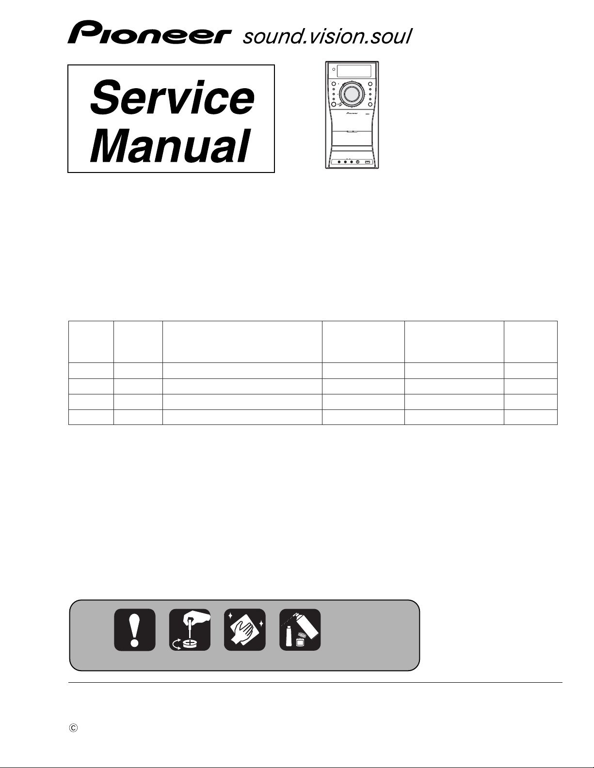
STEREO DVD CASETTE DECK RECEIVER
XV-EV9
THIS MANUAL IS APPLICABLE TO THE FOLLOWING MODEL(S) AND TYPE(S).
Model Type Power Requirement
Regional
restriction codes
(Region No.)
The voltage can be
converted by the
following method.
ORDER NO.
RRV3413
Remarks
XV-EV9 DDRXJ AC 110 V to 127 V / 220 V to 230 V / 240 V 4 With the voltage selector
XV-EV9 DDXJ/RB AC 110 V to 127 V / 220 V to 230 V / 240 V 2 With the voltage selector
XV-EV9 DLXJ AC 110 V to 127 V / 220 V to 230 V / 240 V 3 With the voltage selector
XV-EV9 MTXJ AC 220 V to 240 V 3 –––––
For details, refer to "Important Check Points for Good Servicing".
T-ZZK AUG. 2006 printed in Japan
Page 2
1234
SAFETY INFORMATION
A
This service manual is intended for qualified service technicians ; it is not meant for the casual doit-yourselfer. Qualified technicians have the necessary test equipment and tools, and have been
trained to properly and safely repair complex products such as those covered by this
manual.Improperly performed repairs can adversely affect the safety and reliability of the product
and may void the warranty. If you are not qualified to perform the repair of this product properly and
safely, you should not risk trying to do so and refer the repair to a qualified service technician.
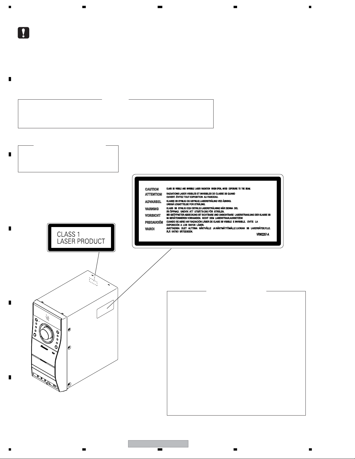
WARNING !
THE AEL (ACCESSIBLE EMISSION LEVEL) OF THE LASER POWER OUTPUT IS LESS THAN CLASS 1
BUT THE LASER COMPONENT IS CAPABLE OF EMITTING RADIATION EXCEEDING THE LIMIT FOR
B
CLASS 1.
A SPECIALLY INSTRUCTED PERSON SHOULD DO SERVICING OPERATION OF THE APPARATUS.
LASER DIODE CHARACTERISTICS
FOR DVD : MAXIMUM OUTPUT POWER : 6 mW
FOR CD : MAXIMUM OUTPUT POWER : 7 mW
WAVELENGTH : 650 nm
WAVELENGTH : 780 nm
LABEL CHECK
C
Printing on Rear Panel
D
E
VRW2257
Additional Laser Caution
1. Laser Interlock Mechanism
• Loading switch (S101 on the LOAB Assy) is used for interlock
mechanism of the laser.
When this switch turned ON in SW2 (CLOSE) side (OPEN signal is
0V and CLOSE signal is 3.5V), a laser becomes the status which can
completely oscillation.
Furthermore, the laser completely oscillates in the disc judgment and
disc playback.
When player is power ON state and laser diode is not completely
oscillating, 780nm laser diode is always oscillating by half power.
• Laser diode is driving with Q307 (650nm LD) and Q308 (780nm LD)
on the DVDM Assy.
Therefore, when short-circuit between the emitter and collector of these
transistors or the base voltage is supplied for transistors turn on, the
laser oscillates. (failure mode)
• In the test mode ∗ , there is the mode that the laser oscillates except
for the disc judgment and playback. LD ON mode in the test mode
oscillates with the laser forcibly.
The interlock mechanism mentioned above becomes invalid in this
mode.
2. When the cover is open, close viewing through the objective lens with
the naked eye will cause exposure to the laser beam.
F
2
1234
XV-EV9
∗ : Refer to page 85.
Page 3
5678
[Important Check Points for Good Servicing]
In this manual, procedures that must be performed during repairs are marked with the below symbol.
Please be sure to confirm and follow these procedures.
1. Product safety
Please conform to product regulations (such as safety and radiation regulations), and maintain a safe servicing environment by
following the safety instructions described in this manual.
1 Use specified parts for repair.
Use genuine parts. Be sure to use important parts for safety.
2 Do not perform modifications without proper instructions.
Please follow the specified safety methods when modification(addition/change of parts) is required due to interferences such as
radio/TV interference and foreign noise.
3 Make sure the soldering of repaired locations is properly performed.
When you solder while repairing, please be sure that there are no cold solder and other debris.
Soldering should be finished with the proper quantity. (Refer to the example)
4 Make sure the screws are tightly fastened.
Please be sure that all screws are fastened, and that there are no loose screws.
5 Make sure each connectors are correctly inserted.
Please be sure that all connectors are inserted, and that there are no imperfect insertion.
6 Make sure the wiring cables are set to their original state.
Please replace the wiring and cables to the original state after repairs.
In addition, be sure that there are no pinched wires, etc.
7 Make sure screws and soldering scraps do not remain inside the product.
Please check that neither solder debris nor screws remain inside the product.
8 There should be no semi-broken wires, scratches, melting, etc. on the coating of the power cord.
Damaged power cords may lead to fire accidents, so please be sure that there are no damages.
If you find a damaged power cord, please exchange it with a suitable one.
9 There should be no spark traces or similar marks on the power plug.
When spark traces or similar marks are found on the power supply plug, please check the connection and advise on secure
connections and suitable usage. Please exchange the power cord if necessary.
0 Safe environment should be secured during servicing.
When you perform repairs, please pay attention to static electricity, furniture, household articles, etc. in order to prevent injuries.
Please pay attention to your surroundings and repair safely.
A
B
C
D
2. Adjustments
To keep the original performance of the products, optimum adjustments and confirmation of characteristics within specification.
Adjustments should be performed in accordance with the procedures/instructions described in this manual.
3. Lubricants, Glues, and Replacement parts
Use grease and adhesives that are equal to the specified substance.
Make sure the proper amount is applied.
4. Cleaning
For parts that require cleaning, such as optical pickups, tape deck heads, lenses and mirrors used in projection monitors, proper
cleaning should be performed to restore their performances.
5. Shipping mode and Shipping screws
To protect products from damages or failures during transit, the shipping mode should be set or the shipping screws should be
installed before shipment. Please be sure to follow this method especially if it is specified in this manual.
56
XV-EV9
E
F
3
7
8
Page 4

1234
CONTENTS
SAFETY INFORMATION..................................................................................................................................... 2
1. SPECIFICATIONS ............................................................................................................................................ 5
2. EXPLODED VIEWS AND PARTS LIST ............................................................................................................ 6
A
B
C
D
E
F
2.1 PACKING ................................................................................................................................................... 6
2.2 EXTERIOR SECTION................................................................................................................................ 8
2.3 AMP SECTION ........................................................................................................................................ 10
2.4 FRONT PANEL SECTION ....................................................................................................................... 12
2.5 06 LOADER ASSY................................................................................................................................... 14
2.6 TRAVERSE MECHANISM ASSY-S ......................................................................................................... 16
2.7 DECK MECHANISM UNIT....................................................................................................................... 17
3. BLOCK DIAGRAM AND SCHEMATIC DIAGRAM ..........................................................................................18
3.1 BLOCK DIAGRAM ................................................................................................................................... 18
3.2 OVERALL WIRING CONNECTION DIAGRAM and LOAB ASSY ........................................................... 20
3.3 DVDM ASSY (1/2).................................................................................................................................... 22
3.4 DVDM ASSY (2/2).................................................................................................................................... 24
3.5 MAIN ASSY (1/3) ..................................................................................................................................... 26
3.6 MAIN ASSY (2/3) ..................................................................................................................................... 28
3.7 MAIN ASSY (3/3) ..................................................................................................................................... 30
3.8 EVOL ASSY............................................................................................................................................. 32
3.9 DISPLAY and HP/MIC ASSYS................................................................................................................. 34
3.10 PRIMARY and TRADE ASSYS.............................................................................................................. 36
3.11 AMP ASSY............................................................................................................................................. 38
3.12 WAVEFORMS........................................................................................................................................ 40
4. PCB CONNECTION DIAGRAM ..................................................................................................................... 42
4.1 LOAB ASSY............................................................................................................................................. 42
4.2 TRADE ASSY .......................................................................................................................................... 43
4.3 DVDM ASSY............................................................................................................................................ 44
4.4 MAIN ASSY ............................................................................................................................................. 48
4.5 EVOL ASSY............................................................................................................................................. 52
4.6 DISPLAY and HP/MIC ASSYS................................................................................................................. 54
4.7 PRIMARY ASSY ...................................................................................................................................... 56
4.8 AMP ASSY............................................................................................................................................... 60
5. PCB PARTS LIST ........................................................................................................................................... 62
6. ADJUSTMENT ............................................................................................................................................... 77
6.1 DECK SECTION ...................................................................................................................................... 77
6.1.1 ADJUSTMENT CONDITION ............................................................................................................. 77
6.1.2 PLAYBACK and RECORDING SECTION ......................................................................................... 78
6.2 DVD SECTION......................................................................................................................................... 80
6.2.1 ADJUSTMENT ITEMS AND LOCATION........................................................................................... 80
6.2.2 JIGS AND MEASURING INSTRUMENTS ........................................................................................ 80
6.2.3 NECESSARY ADJUSTMENT POINTS............................................................................................. 81
6.2.4 TEST MODE ...................................................................................................................................... 82
6.2.5 MECHANISM ADJUSTMENT............................................................................................................ 83
7. GENERAL INFORMATION ............................................................................................................................. 85
7.1 DIAGNOSIS ............................................................................................................................................. 85
7.1.1 TEST MODE ...................................................................................................................................... 85
7.1.2 DISPLAY SPECIFICATION OF THE TEST MODE............................................................................ 86
7.1.3 FUNCTIONAL SPECIFICATION OF THE SHORTCUT KEY ............................................................ 87
7.1.4 SPECIFICATION OF MODEL INFORMATION DISPLAY.................................................................. 88
7.1.5 FUNCTIONAL SPECIFICATION OF THE SERVICE MODE............................................................. 89
7.1.6 SERVICE TEST MODE ..................................................................................................................... 90
7.1.7 METHOD FOR DIAGNOSING DEGRADATION OF THE LDs ON THE PICKUP ASSY................... 92
7.1.8 DVD TROUBLE SHOOTING.............................................................................................................. 93
7.1.9 ID NUMBER AND ID DATA SETTING ............................................................................................... 96
7.1.10 DISASSEMBLY ................................................................................................................................ 99
7.2 PARTS.................................................................................................................................................... 111
7.2.1 IC ..................................................................................................................................................... 111
7.3 EXPLANATION ...................................................................................................................................... 114
7.3.1 SEQUENCE AFTER POWER ON................................................................................................... 114
7.3.2 PROTECTION CIRCUIT.................................................................................................................. 115
8. PANEL FACILITIES ...................................................................................................................................... 120
4
1234
XV-EV9
Page 5
5678
1. SPECIFICATIONS
• Amplifier section
EV7DVD/EV9DVD model
Continuous power output:
Front . . . . . . . . . . . . . . . . . . . 100 W per channel
(1 kHz, 10 % T.H.D., 6 Ω)
Center . . . . . . . 100 W (1 kHz, 10 % T.H.D., 6 Ω)
Surround . . . . . . . . . . . . . . . . 100 W per channel
(1 kHz, 10 % T.H.D., 6 Ω)
Subwoofer. . . 100 W (100 Hz, 10 % T.H.D., 6 Ω)
EV5DVD model
Front . . . . . . . . . . . . . . . . . . . 100 W per channel
(1 kHz, 10 % T.H.D., 6 Ω)
• Disc section
Digital audio
characteristics . . . . . . . . . DVD fs: 96 kHz, 24-bit
Type . . . . . . DVD system, Video CD/Super VCD
system and Compact Disc digital audio system
Frequency response . . . . . . . . . 20 Hz to 44 kHz
S/N ratio. . . . . . . . . . . . . . . . . . . . . . . . . . . 88 dB
Dynamic range. . . . . . . . . . . . . . . . . . . . . . 83 dB
Total harmonic distortion . . . . . . . . . . . . . 0.01 %
Wow and Flutter . . . . . . . . Limit of measurement
(±0.001 % W.PEAK) or less (JEITA)
• Cassette deck section
Systems. . . . . . . . . . . . 4 track, 2-channel stereo
Heads . . . . . . . . . . Recording/playback head x 1
Erasing head x 1
Motor . . . . . . . . . . . . . . . . . . DC servo motor x 1
Tape types . . . . . . . . . . . . . . . . . Type I (Normal)
• FM tuner section
Frequency range . . . . . . . 87.5 MHz to 108 MHz
Antenna . . . . . . . . . . . . . . . . . 75 Ω, unbalanced
• AM tuner section
Frequency range
With 9 kHz step. . . . . . . . 531 kHz to 1602 kHz
With 10 kHz step. . . . . . . 530 kHz to 1700 kHz
Antenna. . . . . . . . . . . . . . . . . . . . . Loop antenna
• Miscellaneous
Power requirements
Multi voltage model
. . . . . . . . AC 110 V to 127 V / 220 V to 230 V /
240 V (switchable), 50 Hz / 60 Hz
Power consumption
EV7DVD/EV9DVD model. . . . . . . . . . . .168 W
EV5DVD model . . . . . . . . . . . . . . . . . . .121 W
Power consumption in standby mode . . . . 0.5 W
Dimensions:
DVD Tuner Deck Receiver
. . . 170 mm (W) x 352.5 mm (H) x 340.1 mm (D)
Weight:
DVD Tuner Deck Receiver . . . . . . . . . . . . 7.2 kg
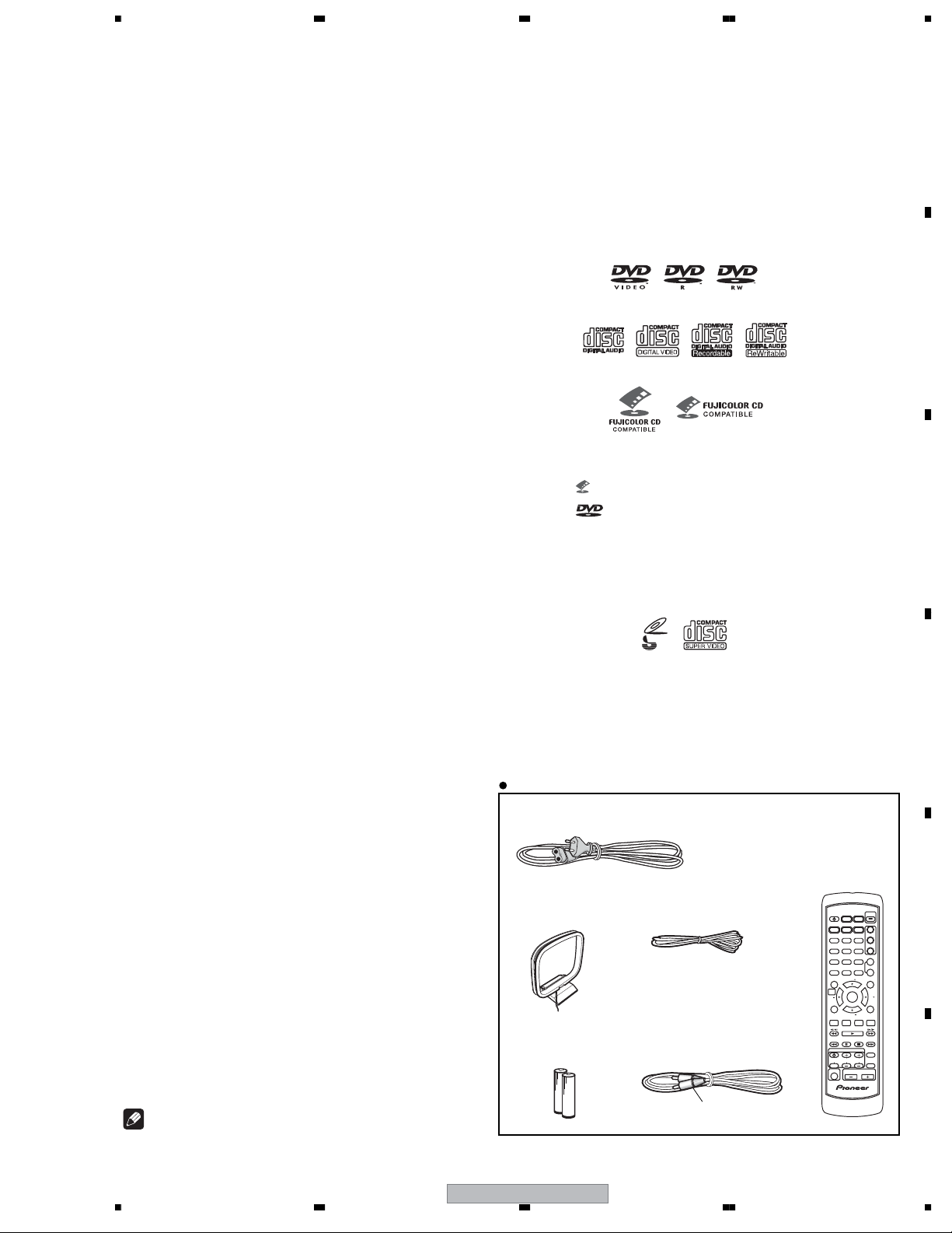
• Accessories (Stereo DVD Tuner Deck)
Remote control . . . . . . . . . . . . . . . . . . . . . . . . . 1
Power cord
Central and South American, Taiwan,
Philippines models. . . . . . . . . . . . . . . . . . . . . 2
Duty Free model. . . . . . . . . . . . . . . . . . . . . . .3
All other models. . . . . . . . . . . . . . . . . . . . . . . 1
Power plug adapter (Central and South American,
and US Military models only). . . . . . . . . . . . . . . 1
Video cord. . . . . . . . . . . . . . . . . . . . . . . . . . . . . 1
AM loop antenna. . . . . . . . . . . . . . . . . . . . . . . . 1
FM antenna. . . . . . . . . . . . . . . . . . . . . . . . . . . . 1
Dry cell batteries (AA/R6) . . . . . . . . . . . . . . . . . 2
Warranty Card (US Military and Duty Free models
only). . . . . . . . . . . . . . . . . . . . . . . . . . . . . . . . . . 1
Operating instructions
• Specifications and design subject to possible
Note
modification without notice, due to improvements.
Disc / content format playback
compatibility
This player is compatible with a wide range of
disc types (media) and formats. Playable discs
will generally feature one of the following logos
on the disc and/or disc packaging. Note
however that some disc types, such as
recordable CD and DVD, may be in an
unplayable format.
See the About DualDisc playback below for
more information.
DVD-Video DVD-R DVD-RW
Audio CD CD-R
• This unit will play DVD+R/+RW discs.
•
•
Licensing Corporation.
• Also compatible with KODAK Picture CD.
This player supports the IEC's Super VCD standard for superior picture quality, dual
soundtracks, and widescreen support.
Manufactured under license from Dolby
Laboratories.“Dolby”, “Pro Logic” and the double-D
symbol are trademarks of Dolby Laboratories.
“DTS” and “DTS Digital Surround” are registered
trademarks of Digital Theater Systems, Inc.
Accessories
• Power Cord
(ADG1154) (DDRXJ : XDG3009)
• AM Loop Antenna
(ATB7013)
• Dry Cell Batteries
Video CD
Fujicolor CD
is a trademark of Fuji Photo Film Co. Ltd.
is a trademark of DVD Format/Logo
VIDEO
CD
Super Video CD (Super VCD)
• FM Antenna (ADH7030)
• Video Cord
(L = 1.5m) (XDE3046)
Yellow
CD-RW
• Remote Control
(XXD3111)
STANDBY
TUNER
X.BOOM
(FM/AM)
DVD/CD
/ON
PLAY LIST
TAPE
USB
LINE
1
RPT RDM
PGM
2
123
MONO
ST.MEMORY
3
456
KARAOKE
AUDIO
ANGLESUBTITLE
789
ECHO
TIMER
ZOOM
ENTER
CLEAR
0
TUNE
SYSTEM SETUP
TOP MENU
MENU
HOME
MENU
ST
ST
ENTER
CH
TEST
LEVEL
TONE
RETURN
SOUND MODE
TUNE
SURROUND
SFC
EXT PWR
FRT.SURR
TV CONTROL
DISPLAY
CHANNEL
INPUT VOLUME
MUTE
SHIFT
VOLUME
A
B
C
D
E
F
56
XV-EV9
5
7
8
Page 6
1234
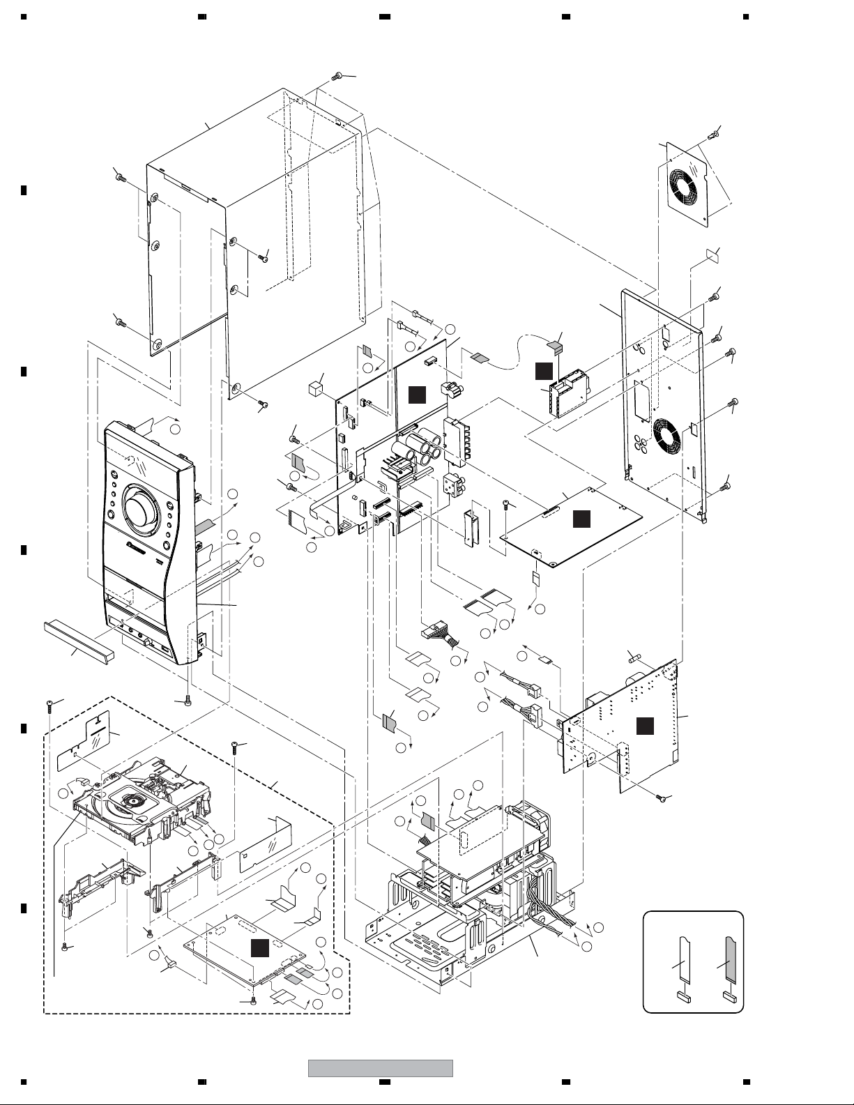
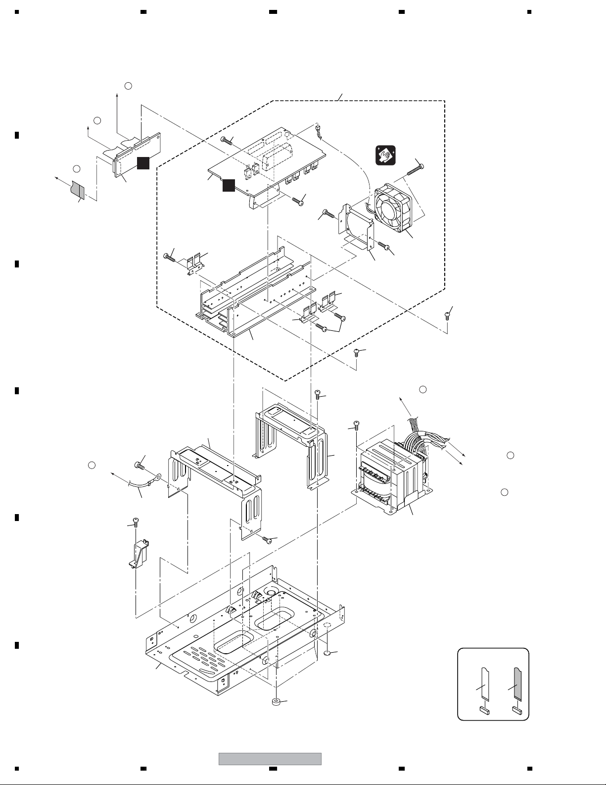
2. EXPLODED VIEWS AND PARTS LIST
NOTES:
Parts marked by "NSP" are generally unavailable because they are not in our Master Spare Parts List.
The mark found on some component parts indicates the importance of the safety factor of the part.
A
Therefore, when replacing, be sure to use parts of identical designation.
Screws adjacent to mark on product are used for disassembly.
For the applying amount of lubricants or glue, follow the instructions in this manual.
(In the case of no amount instructions, apply as you think it appropriate.)
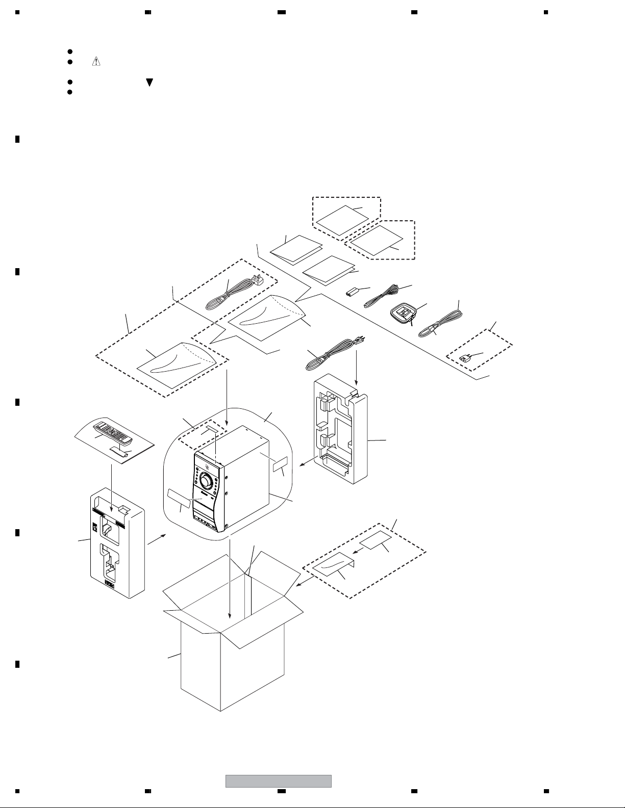
2.1 PACKING
B
C
DDRXJ only
5
10
12
19
3
MTXJ only
15
13
DDRXJ only
16
8
4
9
7
DDRXJ only
Yellow
11
Junction
23
1
DDRXJ or
DDXJ / RB or
DLXJ or
MTXJ
20
MTXJ only
14
6
DDRXJ only
17
18
D
21
E
22
24
2
F
6
1234
XV-EV9
Page 7
>
>
>
>
5678
(1) PACKING SECTION PARTS LIST
No. Description Part No.
Mark
1 Laser Caution VRW2257
NSP 2 Getter Label See Contrast table (2)
3AC Power Cord ADG1154
4 FM Antenna ADH7030
5Polyethylene Bag See Contrast table (2)
No. Description Part No.
Mark
16 Caution Sheet AR See Contrast table (2)
17 Remote Control Unit XXD3111
18 Battery Cover AZN8018
NSP 19 Polyethylene Bag Z21-038
20 Rear Pad XHA3157
A
NSP 6 Polyethylene Bag See Contrast table (2)
7 AM Loop Antenna ATB7013
NSP 8 Dry Cell Batteries (AA/R6) XEX3001
9 Video Cord XDE3046
10 AC Power Cord See Contrast table (2)
11 Power Plug Adapter See Contrast table (2)
12 Operating Instructions (English) See Contrast table (2)
13 Operating Instructions See Contrast table (2)
NSP 14 Warranty Card (Thai) See Contrast table (2)
NSP 15 Service Map (Thai) See Contrast table (2)
21 Front Pad XHA3160
22 Packing Case See Contrast table (2)
23 Packing Sheet XHG3010
NSP 24 DF Label See Contrast table (2)
NSP 25 Label VRW1629
(2) CONTRAST TABLE
XV-EV9/DDRXJ, DDXJ/RB, DLXJ and MTXJ are constracted the same except for the following :
Mark No. Symbol and Description
NSP 2 Getter Label XAX3588 XAX3586 XAX3586 XAX3586
5Polyethylene Bag AHG7033 Not used Not used Not used
NSP 6 Polyethylene Bag Not used Not used Not used AHG7031
>
NSP 14 Warranty Card (THAI) Not used Not used Not used XRY3004
NSP 15 Service Map (THAI) Not used Not used Not used XRY3005
NSP 24 DF Label AAX7960 Not used Not used Not used
10 AC Power Cord XDG3009 Not used Not used Not used
11 Power Plug Adapter XKM3001 Not used Not used Not used
12 Operating Instructions (English) XRB3061 XRB3062 XRB3061 Not used
13 Operating Instructions (Spanish) XRC3232
13 Operating Instructions (Arabic)
13 Operating Instructions (Chinese)
13 Operating Instructions (Thai)
16 Caution Sheet AR XRH3002 Not used Not used Not used
22 Packing Case XHD3648 XHD3649 XHD3647 XHD3651
XV-EV9
/DDRXJ
Not used
Not used Not used
Not used Not used Not used
XV-EV9
/DDXJ/RB
Not used Not used Not used
XRC3234
XV-EV9
/DLXJ
Not used Not used
XRC3231
XV-EV9
/MTXJ
Not used
XRC3233
B
C
D
56
XV-EV9
E
F
7
7
8
Page 8
1234
2.2 EXTERIOR SECTION
A
24
27
26
21
22
B
C
D
23
28
P
E
17
27
Refer to
"2.5 06 LOADER ASSY".
F
26
16
27
27
25
26
19
E
2
20
D
C
C
26
27
A
A
26
C
9
J
1
3
27
26
27
26
27
D
M
6
4
26
B
E
D
Refer to
"2.4 FRONT PANEL
SECTION".
F
B
L
K
F
O
10
J
H
I
N
G
28
14
13
15
S
R
Q
18
12
5
H
M
8
P
B
7
27
11
S
R
Q
I
G
L
K
G
J
O
N
26
Refer to
"2.3 AMP SECTION".
NON-CONTACT
SIDE
CONTACT SIDE
8
1234
XV-EV9
Page 9
>
5678
(1) EXTERIOR SECTION PARTS LIST
No. Description Part No.
Mark
1 FM/AM Tuner Unit AXX7211
NSP 2 MAIN ASSY See Contrast table (2)
NSP 3 EVOL ASSY XWK3261
4 PRIMARY ASSY See Contrast table (2)
5DVDM ASSY AWM8059
No. Description Part No.
Mark
16 Cable Barrier XEC3069
17 Adaptor 05 L XNW3014
18 Adaptor 05 R XNW3015
19 Rear Panel See Contrast table (2)
20 PCB Spacer AEB7206
A
6 Fuse (T4A) REK1028
7 Connector ASSY PG05KK-E10
8 7P F.F.C/60V XDD3208
9 11P F.F.C/60V XDD3179
10 17P F.F.C/60V XDD3180
11 27P F.F.C/60V XDD3206
12 27P F.F.C/60V XDD3207
NSP 13 DVD ASSY XXA3039
NSP 14 06 Loader ASSY VWT1226
15 Mecha Barrier XEC3068
21 Push Rivet XEC3034
22 Fan Barrier XEC3075
23 Tray Cap XAK3537
24 Bonnet Case XZN3186
NSP 25 ID Label ASSY VXW1002
26 Screw BBZ30P080FNI
27 Screw BPZ30P080FNI
28 Screw XBA3015
(2) CONTRAST TABLE
XV-EV9/DDRXJ, DDXJ/RB, DLXJ and MTXJ are constracted the same except for the following :
Mark No. Symbol and Description
NSP 2 MAIN ASSY XWK3254 XWK3255 XWK3254 XWK3256
4 PRIMARY ASSY XWZ4146 XWZ4146 XWZ4146 XWZ4150
19 Rear Panel XNC3443 XNC3444 XNC3442 XNC3446
XV-EV9
/DDRXJ
XV-EV9
/DDXJ/RB
XV-EV9
/DLXJ
XV-EV9
/MTXJ
B
C
D
E
F
56
XV-EV9
9
7
8
Page 10
1234
2.3 AMP SECTION
A
Refer to
"2.2 EXTERIOR
SECTION. "
B
C
Refer to
"2.2EXTERIOR
SECTION. "
Refer to
"2.2 EXTERIOR
SECTION. "
K
G
9
L
19
H
2
19
1
I
4
6
19
19
4
10
19
20
Cleaning paper
GED-008
3
19
5
4
17
17
Refer to
"2.2 EXTERIOR
16
12
D
E
Refer to
"2.4 FRONT PANEL
SECTION. "
T
17
8
16
17
18
13
14
SECTION. "
J
Refer to
"2.2 EXTERIOR
SECTION. "
Refer to
"2.2 EXTERIOR
SECTION. "
7
O
N
11
F
10
1234
XV-EV9
15
NON-CONTACT
SIDE
CONTACT SIDE
Page 11

>
5678
(1) AMP SECTION PARTS LIST
No. Description Part No.
Mark
1 AMP ASSY XWK3262
2 TRADE Assy XWZ4149
3 DC Fan Motor XXM3009
4 FET Bracket ANG7418
5Fan Plate ANG7462
NSP 6 Heat Sink XNH3045
7Audio Next Trans XTS3105
8 Cord With Plug DE015VE0
9 17P F.F.C/60V XDD3180
NSP 10 AMP Unit 6CH XXQ3007
A
NSP 11 Chassis HAL XNA3028
12 AMP Support F XNG3141
13 AMP Support R XNG3150
14 Leg Cushion XEB3050
NSP 15 Spacer AEB7092
16 Screw BBZ30P060FTC
17 Screw BBZ30P080FNI
18 Screw BBZ40P060FTC
19 Screw BBZ30P140FTC
20 Screw BBZ30P300FTC
B
C
D
56
XV-EV9
E
F
11
7
8
Page 12
1234
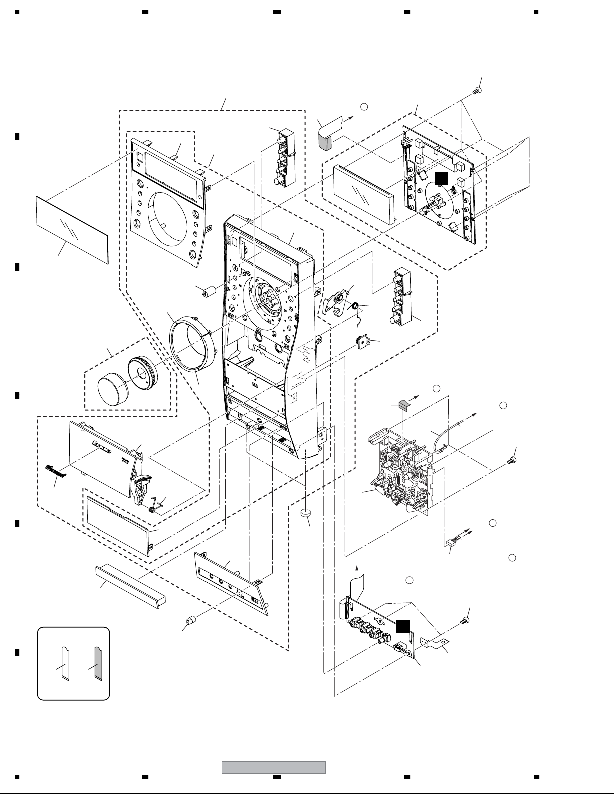
2.4 FRONT PANEL SECTION
A
12
16
20
30
Refer to
"2.2 EXTERIOR
SECTION. "
5
A
1
29
E
B
25
10
18
17
C
9
26
13
16
14
Refer to
"2.2 EXTERIOR
19
23
D
22
24
28
21
8
15
E
11
7
Refer to
"2.7 DECK
MECHANISM
UNIT."
SECTION. "
4
Refer to
"2.2 EXTERIOR
SECTION. "
B
F
3
2
Refer to
C
"2.3 AMP
SECTION. "
Refer to
"2.2 EXTERIOR
SECTION. "
6
29
27
T
29
E
Refer to
"2.2 EXTERIOR
SECTION. "
D
NON-CONTACT
F
12
CONTACT SIDE
SIDE
XV-EV9
1234
Page 13

5678
(1) FRONT PANEL SECTION PARTS LIST
No. Description Part No.
Mark
1 DISPLAY ASSY XWZ4147
2 HP/MIC ASSY XWZ4148
NSP 3 Cord With Plug DE015VE0
4 11P F.F.C/60V XDD3204
5 19P F.F.C/60V XDD3205
6 Cable ASSY XDE3068
7 Deck Mechanism Unit XYM3019
8 MIC Knob XAA3029
9VOL Knob ASSY XAB3044
10 Display Panel XAK3536
A
11 Tray Cap XAK3537
NSP 12 Front Panel ASSY XXG3275
13 Ratch Spring_R ABH7131
14 Damper ASSY AXA7052
15 PIONEER Name Plate VAM1129
16 Sub Button XAD3242
NSP 17 VOL Button XAD3243
18 Timer Lens XAK3506
NSP 19 VOL Cap XAK3539
20 Top Panel XAK3540
21 Bottom Panel XAK3542
NSP 22 Middle Panel XAK3543
23 Deck Door XAN3057
24 Door Spring_R XBH3002
NSP 25 Front Panel XMB3239
26 Ratch Mold_R XMR3002
27 GND Plate XNG3148
28 Leg Cushion XEB3051
29 Screw BPZ30P080FNI
30 Front Panel ASSY XZN3189
B
C
D
56
XV-EV9
E
F
13
7
8
Page 14
1234
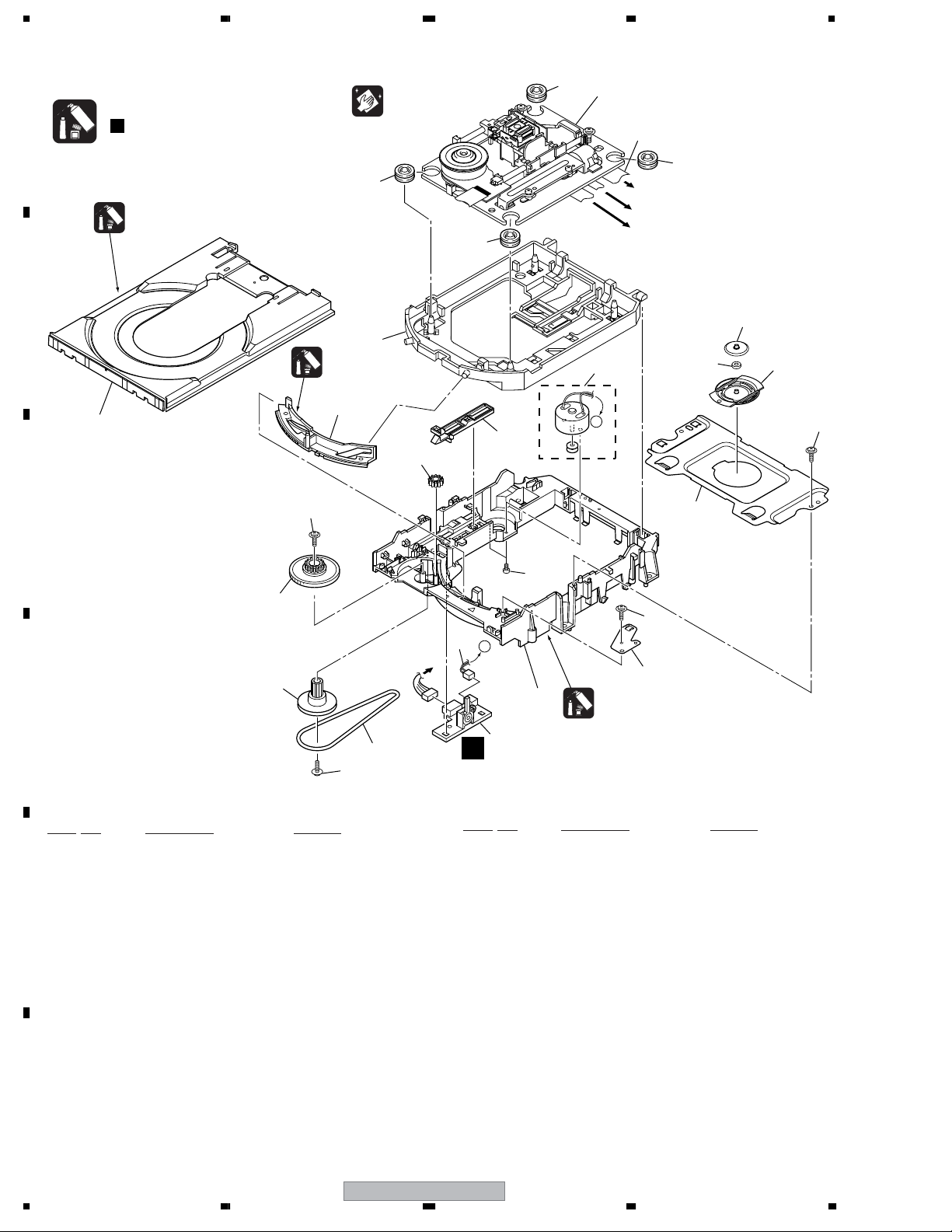
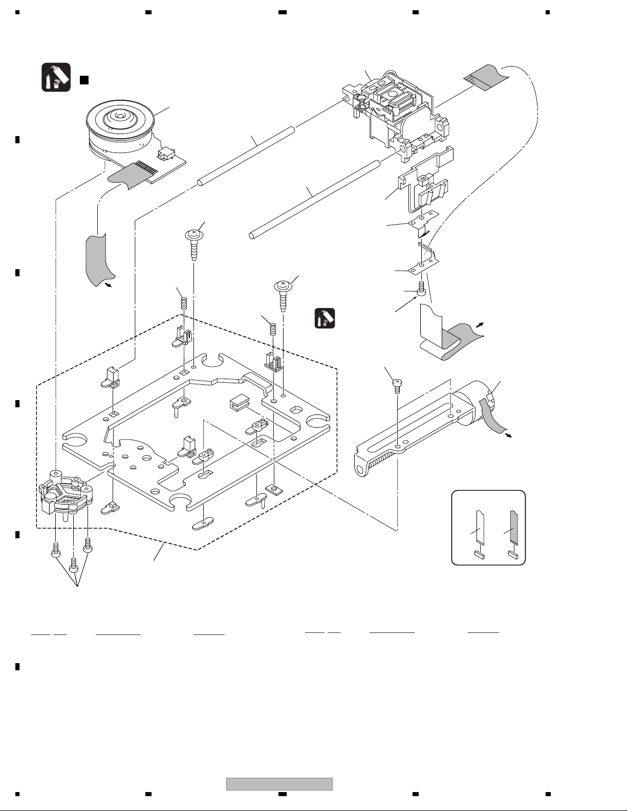
2.5 06 LOADER ASSY
A
B
C
Note :
Refer to
" Application of Lubricant".
Daifree
GEM1036
23
Lubricating Oil
GYA1001
13
22
Pickup leneses
Cleaning liquid
GEM1004
Cleaning paper
GED-008
8
12
16
8
8
17
Refer to
2
"2.6 Traverse Mechanism Assy-S".
6
8
To DVD MAIN CN101 (Pickup)
To DVD MAIN CN104 (Stepping Motor)
To DVD MAIN CN102 (Spindle Motor)
18
3
A
24
19
20
22
15
14
D
06 LOADER ASSY PARTS LIST
Mark
No. Description Part No.
NSP 1 LOAB Assy VWG2346
2Traverse Mechanism Assy-S DXX2575
3 Loading Motor Assy VXX2912
E
4• • • • •
5• • • • •
6 Flexible Cable (24P) ADD7545
7 Connector Assy 2P VKP2253
8 Floating Rubber VEB1351
9 Belt VEB1358
10 Stabilizer VNE2253
22
DVDM CN103
9
21
22
7
To
A
10
11
1
A
Mark
No. Description Part No.
16 Drive Gear VNL1923
17 SW Lever VNL1925
18 Clamper Plate 04 VNE2342
19 Bridge 04 VNE2343
20 Clamper 04 VNL1969
21 Screw JGZ17P028FTC
22 Screw VBA1094
23 Tray VNL1920
24 Clamp Magnet VMG1029
Lubricating Oil
GYA1001
11 Loading Base VNL1917
12 Float Base 04 VNL1968
F
13 Drive Cam VNL1919
14 Gear Pulley VNL1921
15 Loading Gear VNL1922
14
1234
XV-EV9
Page 15
5678
Application of Lubricant
Lubricating Oil
GYA1001
No. 11
Loading Base
No. 13
Drive Cam
Lubricating Oil
GYA1001
Around the shaft
Lubricating Oil
GYA1001
Lubricating Oil
GYA1001
Inner side of a ditch
A
B
Lubricating Oil
GYA1001
Inner side of a ditch
C
Lubricating Oil
GYA1001
Lubricating Oil
GYA1001
Front View Rear View
No. 23
Tray
Daifree
GEM1036
Concave of unevenness
No. 23
Tray
Top View Bottom View
Concave of unevenness
Daifree
GEM1036
Inner side of a ditch
Daifree
GEM1036
No. 13
Drive Cam
D
Daifree
GEM1036
Concave of unevenness
E
Side of the rib
Daifree
GEM1036
F
56
XV-EV9
15
7
8
Page 16
1234
2.6 TRAVERSE MECHANISM ASSY-S
>
Note :
A
B
C
Refer to
" Application of Lubricant".
Note : When part #2 replaced,
2
11
To DVDM CN102
(Spindle Motor)
part #13 also need to be
replaced at the same time.
4
3
10
10
11
1
5
6
14
Silicone Adhesive
GEM1037
9
To
DVDM CN101
(Pickup Assy)
D
8
Note : Spindle screw (DBA1252) of No.13 is the screw which applied special bond.
E
13
Therefore the adhesion becomes inteffective when takes it off once. Spindle screw is the part which cannot recycle.
When part #2 is replaced, part #13 also need to be replaced at the same time.
TRAVERSE MECHANISM ASSY-S PARTS LIST
No. Description Part No.
Mark
1 06SD Pickup Assy OXX8020
2 Spindle Motor N200 DXM1197
NSP 3 Guide Shaft VK1 DLA1940
NSP 4 Sub Guide Shaft VK1 DLA1941
NSP 5 Joint VK1B DNK4272
12
NON-CONTACT
SIDE
No. Description Part No.
Mark
11 Skew Spring VK1 DBH1516
NSP 12 Stepping Screw DBA1205
13 Spindle Screw VK1(for Service) DBA1252
NSP 14 Hold Spring DBK1297
7
To
DVDM CN104
(Stepping Motor)
CONTACT SIDE
NSP 6 Joint Spring VK1 DBK1235
F
7 Stepping Motor VK1 DXM1201
NSP 8 Mechanism Frame VK1 DNK4160
9 Precision Screw VK1 DBA1209
10 Skew Screw VK1 DBA1211
16
1234
XV-EV9
Page 17
5678
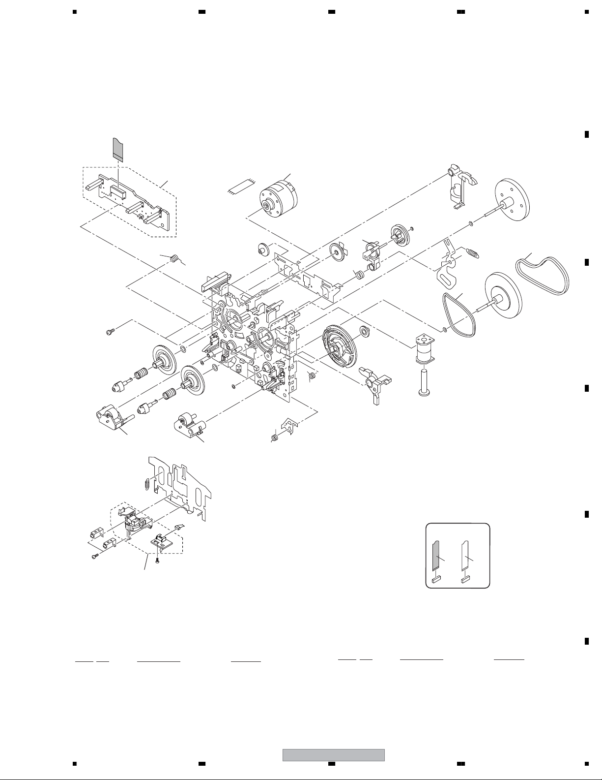
2.7 DECK MECHANISM UNIT
A
8
5
4
7
B
6
1
2
C
D
3
DECK MECHANISM UNIT PARTS LIST
Mark No. Description Part No.
1 Main Belt FF20B-13A
2 F/R Belt FF19S-31
3 Plate HD Blk F513-926
4 Roller Pinch Blk R F514-133
5 Roller Pinch Blk L F514-134
56
CONTACT SIDE
Mark No. Description Part No.
6 Clutch Assy Blk F522-063
7 Motor Main Blk F525-394
8 PCB Control Blk F567-747
XV-EV9
7
NON-CONTACT
SIDE
8
E
F
17
Page 18
MPEG
Video Decoder
Video
Encoder
Video
(withPictureControl)
ressi
54MHz
(VRmode with CPRM)
udio Decoder
-DD MPEG
JPEG
er
WMA Pl
yba
W Pl
yba
64M SDRAM
16M
FLASH
OM
+ -
6IN-6OUT
system control
+ -
Cb/B
Cr/R
CY/G
SPINDLE
03SD PU
*SINGLE DISC MECHA
Load
Motor
Motor
27MHz
Cb
COMPONENT&
COMPOSITE
VIDEO OUT
DECK MECHA
MIC
AMP
Lch
Rch
INPUT
SELEC
OR
UFFER
OCAL
ADER
ALC
ONE
CONT
OL
BASS
BOOST
MAIN
OL
olume Chip
(MAIN)
MIC
(SW C)
Stepping
Motor
VIDEO AMP
er Mode
1234
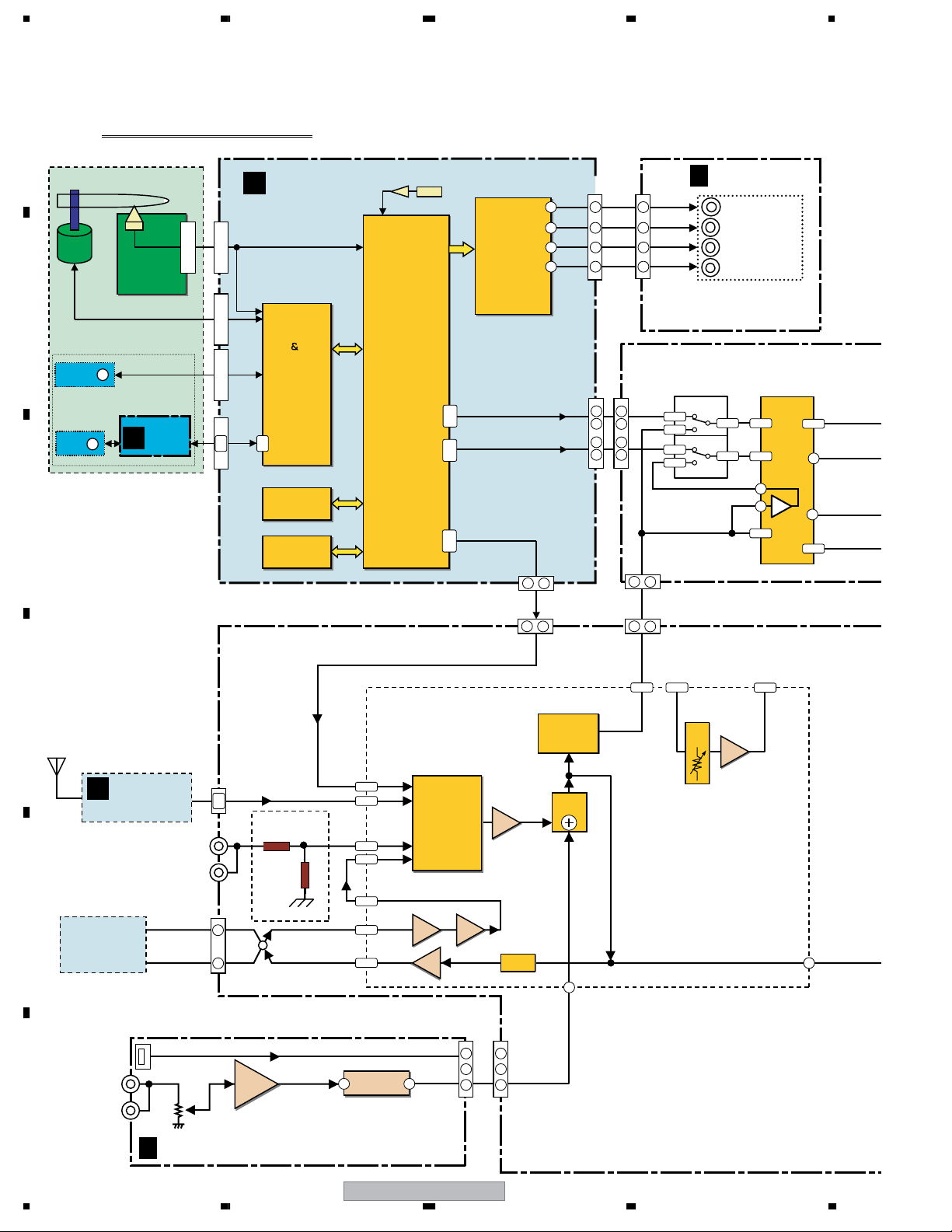
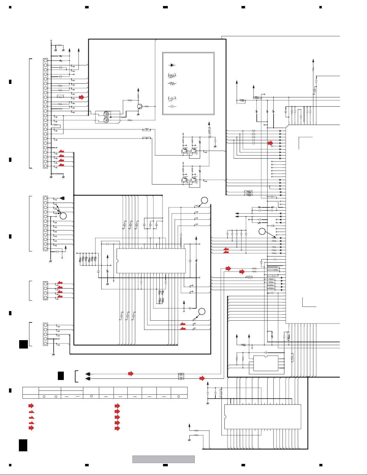
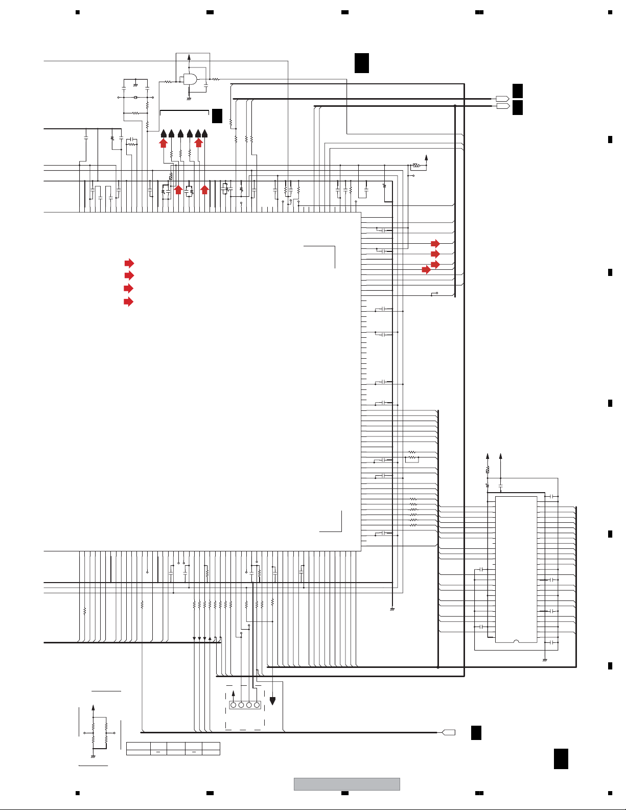
3. BLOCK DIAGRAM AND SCHEMATIC DIAGRAM
3.1 BLOCK DIAGRAM
A
AUDIO NEXT Block Diagram
16
20
18
23
27
27
CN902(1/2)
(27P)
R
16
Y
12
Cb
14
V
8
CN903
(7P)
5
7
1
3
CN3001(2/2)
(27P)
5
7
1
3
B
C
SPINDLE
Motor
*SINGLE DISC MECHA
Stepping
M
+ -
Motor
Load
M
+ -
Motor
03SD PU
PlCK UP
ASSY
LOAB
A
ASSY
CN1013
(24P)
CN101
(24P)
CN102
(12P)
CN103
(4P)
1
2
CN104
(5P)
DVDM ASSY
B
FTS SPDL
DRlVER
IC101
BD7995EFS
1
2
IC202
64M SDRAM
IC203
16M
FLASH
ROM
BACK END IC
IC201
MT1389FE/H-L
system control
MPEG
Video Decoder
Video
Encoder
(withPictureControl)
Video
DAC
(Progressi
Audio Decoder
-DD MPEG
JPEG
ViViewer
WMA Pl
ayba
RW Pl
ayba
(VRmode with CPRM)
27MHz
ve: 54MHz
ck
ck
FL/FR
)
223
227
222
228
224
226
CN902(2/2)
VIDEO AMP
DRIVER
IC401
MM1758XF
6IN-6OUT
(SL SR)
(SW C)
(27P)
25
25
16
12
14
CN8002
(7P)
1
1
CN3001
8
(1/2)
C
(27P)
Cr/R
CY/G
Cb/B
V
Extra Power Mode
IC8402,8403
HEF4066BT
IC8402
1,11
4,8
IC8403
1,11
4,8
CN8001(2/2)
(23P)
3
3
CN3004
(23P)
2/2
COMPONENT&
COMPOSITE
VIDEO OUT
2,10
2,10
(1/2)
MAIN ASSY
JA8801
IC8401
BD3814FV
11,13
E-VOL
9,15
3
1
17,19
27,28
32
29
30,31
D
E
F
18
FM/AM
J
TUNER
UNIT
DECK MECHA
JA5402
(MAIN)
JA5403
(SUB)
1234
LINE
IN
JA5401
USB JACK
F
1/2
CN2301
(4P)
CN5505
(11P)
6
8
JA3001
(R)
(L)
Lch
3
Rch
1
MIC
AMP
VOL
IC5401
MIC
HP/MIC ASSY
TXR/TXL
ATTENUATOR
(- 6dB)
IC3001
BD3401KS2
E Volume Chip
63,64
61,62
59,60
3,4
6,7
9,10
14,15
MIC ECHO
IC5402
9 8
M65855FP
INPUT
SELEC
CN5401
XV-EV9
(13P)
TOR
323
7
BUFFER
ALC
2
CN3301(1/2)
(13P)
7
37,39
36,38
TONE
CONT
ROL
VOCAL
FADER
58
MAIN
VOL
BASS
BOOST
32,33
55
Page 19
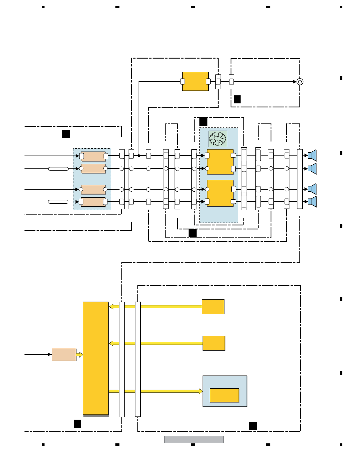
wer Amp
FL/FR
SW
SL/SR
ANDREW CIRCUIT
WER AMP
NJM4565MD
NJM4565MD
NJM4565MD
wer Amp
NJM4565MD
micro
Proccseor
NJM4565MD
PDC139
IC5501
SENSOR
KEY
EVOL ASSY
D
FL/FR
SW
X-BOOM
MUSIC/MOVE
IC8502
NJM4565MD
C
SL/SR
FRONT SURR
IC8405,8406,8407
NJM4565MD
5678
A
J5401
(13P)
3
IC8501
5
NJM4565MD
IC8504(2/2)
5
NJM4565MD
ANDREW CIRCUIT
IC8504(1/2)
3
NJM4565MD
IC8503
3
5
NJM4565MD
HEADPHONE
AMP
3
5
IC3110
NJM4565MD
1
7
CN3301(2/2)
(13P)
11
11
13
13
F
2/2
HP/MIC ASSY
AMP ASSY
I
CN8001
(2/2)
(23P)
13
13
1
7
7
1
1
7
15
19
17
21
23
15
19
17
21
23
CN3004
(2/2)
(23P)
CN3003
(17P)
7
9
13
11
15
17
CN3031
(17P)
7
9
13
11
15
17
17
19
20
21
22
23
CN3021
(23P)
CN3002
(23P)
17
19
20
21
22
23
TRADE ASSY
H
IC3401
11
15
STK433-270
3ch
16
Power Amp
IC3301
16
STK433-270
3ch
Power Amp
11
15
POWER AMP
MODULE
4-7
18
19
18
19
4-7
18
19
22
23
14
15
10
11
3
4
7
8
CN3001
(23P)
CN3022
(23P)
18
19
22
23
14
15
10
11
3
4
7
8
J3032
(12P)
CN3302
(12P)
1
1
4
4
6
6
8
8
10
10
12
12
JA3301
(12P)
HEADPHONE
JACK
JA5404
FL/FR
OUT
SW
OUT
CENTER
OUT
SL/SR
OUT
B
C
Level
Circuit
Detector
CN5301
C
1/2
CN5504
(19P) (19P)
PDC139
IC5501
micro
Proccseor
MAIN ASSY
XV-EV9
56
S5308-S5321
KEY
X5302
IR
SENSOR
FL DISPLAY
XAV3032
FL DRIVER
PT6324-Q(L)
IC5301
D
E
F
DISPLAY ASSY
E
19
7
8
Page 20
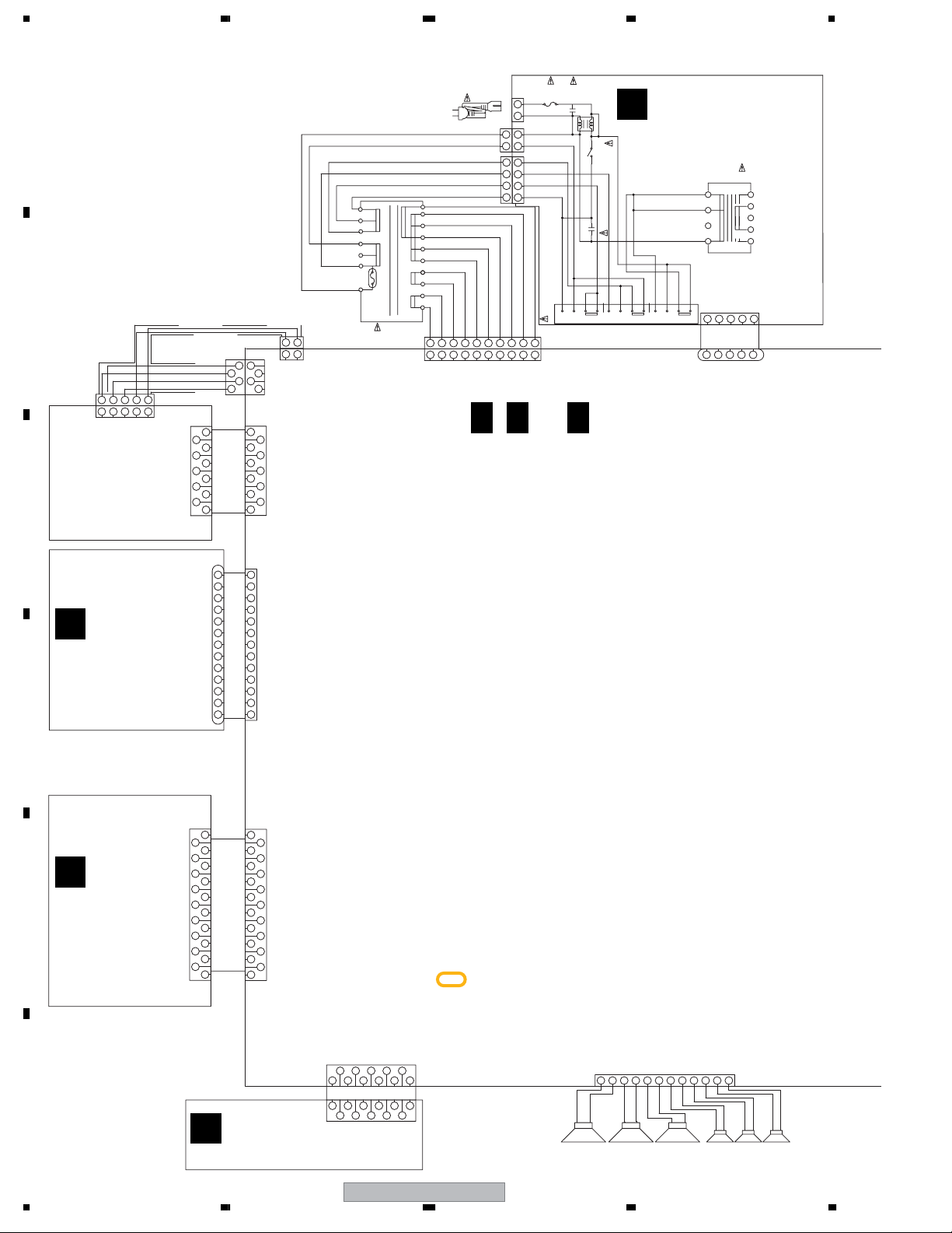
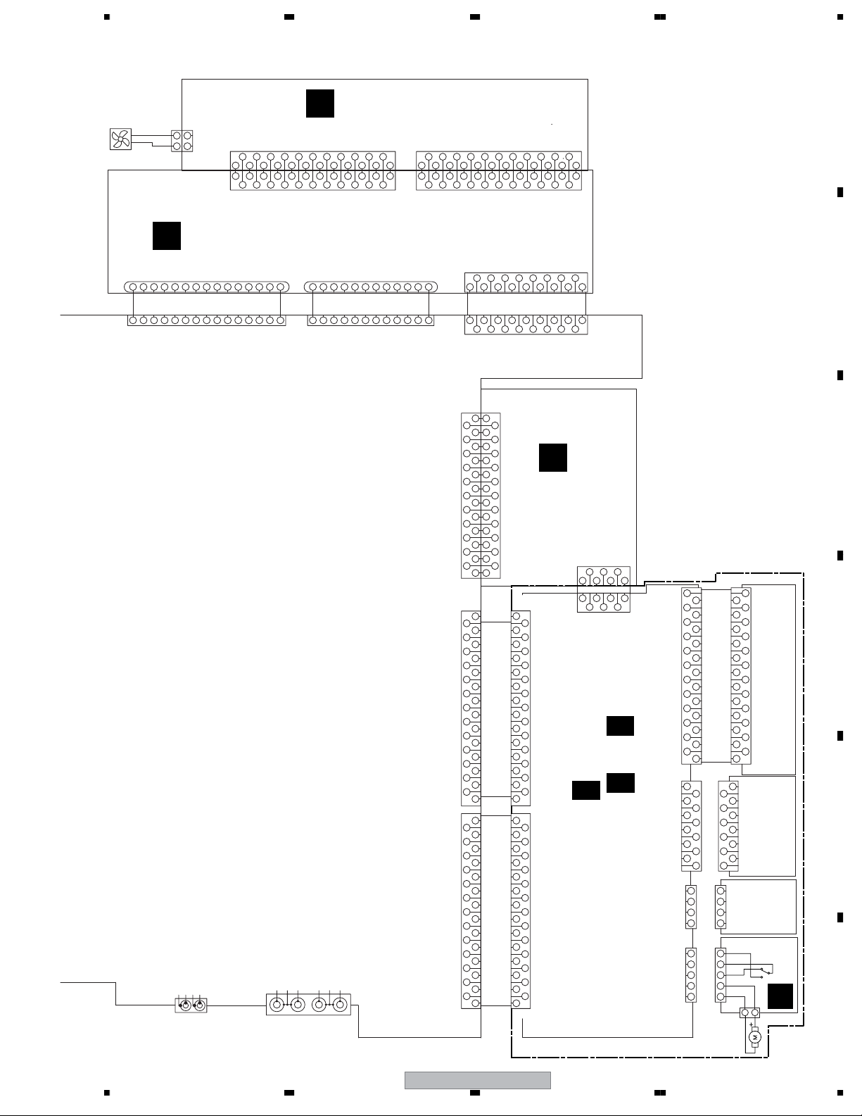
1234
3.2 OVERALL WIRING CONNECTION DIAGRAM and LOAB ASSY
FU1
A
B
CN8010
CN8011
TAPE DECK
MECHA
C
(XYM3017)
F
HP/MIC ASSY
(XWZ4148)
D
1234
1234
L CH
R CH
VREF
Deck Shield Wire 5P
5
5
CN8012
BIAS
GNDM
VREF
PULSE
MODE
GNDM(TC)
VD+5V
MOTOR
RECR
434
XDE3068
SOL
NC
HALF
RECF
1221
1
2
3
410
5
6
XDD3204
7
8
119
11P FFC
J5401
51048-1300
1
V +5USB V +5USB
2
D-
D+
3
GND USB
4
MIC SW
5
GNDA
6
MIC
7
D20PYY1330E
VA+12
8
ECHOVOL
9
10
HPDET
11
HPR
12
GNDHP
13
HPL
GNDA
3
L CH
GNDA
R CH
B4B-PH-K-S
CN2301
1
GNDM
2
SOL
3
NC
4
PULSE
5
HALF
6
MODE
7
GNDM(TC)
8
VD+5V
RECF
10
MOTOR
119
RECR
CN5503
CKS 3376
CN3301
52147-1310
1
2
D-
D+
3
4
GND USB
MIC SW
5
GNDA
6
MIC
7
VA+12
8
ECHOVOL
9
HPDET
10
11
HPR
12
GNDHP
HPL
13
1
1
2
2
GND
B2B-PH-K-S
120
10
0
120
120
CN2302
0
0
T1*
XTS3105
CN11
B10PS-VH
AN1
XKP3084
LIVE
2
1
NEUTRAL
2
2
1
1
4
4
32
3
2
1
67834512
GND
BLAC2
BHAC2
1
BLAC1
VFDP
BHAC1
BLAC1
GND
BLAC2
BHAC2
SUBAC1
SUBAC1
FLAC1
FLAC2
10 9
10 9
FLAC1
FLAC2
78645312
SUBAC1
SUBAC1
C C C( 1/3- 3/3)
MAIN ASSY
(XWK3254:DDRXJ,DLXJ)
(XWK3255:DDXJ/RB)
(XWK3256:MTXJ)
REK1028
CN1
B2P3-VH
0v
120v
0v
0v
10v
120v
CN2
BHAC1
H1
B4P7-VH
S1
VFDP
C1
H2
ACE7013
0.01
STDBY
L1
RY81
XSR3008
C3
0.01
ACE7013
baecd f g h
XKX3001
PRIMARY ASSY
G
(XWZ4146:DDRXJ,
DDXJ/RB,DLXJ)
(XWZ4150:MTXJ)
100VNC230V
120V
NC
NC
0V
ijkl
NC
NC NC NC
0V 0V 0V
T2
ATT7080
230V
19
115V
2
3
45
52147-0510
CN3
SYSPOW
SUBAC
GNDU
12 4355
D2OPYY0525E
1234
J12
51048-0500
GNDU
SUBAC
SYSPOW
VE+5
8
7
6
VE+5
XPROT
XPROT
E
DISPLAY
E
ASSY
(XWZ4147)
F
20
XDD3205
9
7
5
3
19P FFC
1
FM/AM
TUNER
19
17
15
13
11
9
7
5
3
1
VKN1250
18
16
14
12
10
8
6
4
2
VFL+5
VFDP
FLCS
FLCK
FLDATA
GNDFL
MUSICLED
MOVIELED
FLAC2
FLAC1
GNDLED
KEY1
KEY2
JOG
VE+5
VP+12
GNDU
REMOCON
TIMERLED
GND
NC(VSM)
RDS
10
11
9
CKS3376
CN5505
11
9
10
RDS
GND
NC(VSM)
NOTES: • When ordering service parts, be sure to refer to “EXPLODED
VIEWS and PARTS LIST” or “PCB PARTS LIST”.
• The > mark found on some component parts indicates the
importance of the safety factor of the part.
Therefore, when replacing, be sure to use parts of identical
designation.
• : The power supply is shown with the marked box.
CLK
TXR
+9V
TXLDODICEGND
8
6
2
4
1
3
7
5
11P FFCXDD3179
5
1
3
7
4
8
6
2
DI
CE
DO
+9V
TXL
CLK
TXR
GND
Speaker for FL/FR
2134586
7
9
10
Speaker for SL/SR/C/SW
11
12
XKE3051
JA3301
19
VFL+5
18
VFDPVFDP
17
FLCS
16
FLCK
15
FLDATA
14
GNDFL
MUSICLED
13
MOVIELED
12
11
FLAC2
10
FLAC1
GNDLED
8
KEY1
KEY2
6
JOG
VE+5
VP+12
4
GNDU
REMOCON
2
TIMERLED
VKN1250
CN5301 CN5504
J
UNIT(AXX7211)
XV-EV9
1234
Page 21
5678
XXM3009
51048-1500
52147-1510
FAN
2
1
VH+
12 534
VH+
CN13 J3033
CN8004
H
VH+
UN+8V
GNDF
21534
VH+
GNDF
UN+8V
AMP ASSY
I
VP+12
VP+12
VFL+5
111413
11
VFL+5
MUTE
MUTEC
RYFS
12
15
13
15
1412181620
RYFS
MUTE
MUTEC
VPR+8
VPR+8
(XWK3262)
GNDA
FRIN
FLIN
VPR+8
CIN
SRIN
SLIN
SWIN
16
VPR+8
22
20
17
19
23
21
XKP3071
23
21
191817
22
XKP3055
CIN
FLIN
SLIN
FRIN
SRIN
SWIN
GNDA
VH-
VH-
SROUT
SROUT
2
4
113
CN3001
3
4
2
VH-
VH-
SROUT
SROUT
CN3022
5
5
GNDP
GNDP
GNDP
SLOUT
SLOUT
GNDS
VH+
COUT
COUT
VH+
12
10
876
111413
799
13
11
101412
8
6
VH+
VH+
COUT
COUT
GNDP
GNDS
SLOUT
SLOUT
CN3651
KM200SA2
1
1
2
2
RYRC
1
XKP3071
CN3002
1
XKP3055
RYRC
CN3021
2
2
GNDF
GNDF
3
3
UN+8V
4
4
UN+8V
UN+8V
5
5
UN+8V
GNDREG
GNDREG
6
6
GNDREG
GNDREG
XPROT
7109
7
XPROT
VD+5
VA-1 2
8
9
10
8
VD+5
VA-1 2
TRADE ASSY
(XWZ4149)
RYFS
XPROT
RYRC
GNDA
MUTEC
MUTE
UN+8V
GNDREG
VL+
VL+
GNDP
GNDS
GNDP
VL-
VL-
VH-
78691011 13 1412
D20PYY1515E
78610119121314
VL+
VL+
GNDREG
GNDP
XKB3057
JA3001
UN+8V
GNDP
GNDS
VL-
VL-
VH-
VH-
15 21534
15 21 345
VH-
51048-1200
52147-1210
CN3302 J3032
FLOUT
FLOUT
VPR+8
VPR+8
VPR+8
VPR+8
VFL+5
FROUT
D20PYY1215E
VFL+5
FROUT
XKB3058
VP+12
SWOUT
SLOUT
COUT
7861011912
7861011912
COUT
VP+12
SWOUT
JA8801
SROUT
VA-12
VD+5
VD+5
VA-1 2
SLOUT
SROUT
DVDPOWER
NC(ASPECT)
NC(SQUEEZE)
NC(TRKUP)
NC(VSEL1)
NC(VSEL2)
CN3001 CN902
R/Cr
B/Cb
G/Cy
LINE IN
Video
VIDEO/COMPONENT OUT
56
2
1
34765
321
4
RYFS
RYRC
MUTE
GNDA
XPROT
MUTEC
CN3004 CN8001
XKM3006 XKP3055
FL
1
1
FL
GNDA
FR
VA+12
EXPWRM
E-CLK
E-DATA
FRTSURR
MUSIC
MOVIE
ABYPASS
VA-12
FLIN
GNDA
FRIN
GNDA
CIN
GNDA
SWIN
GNDA
SLIN
GNDD
SRIN
CN5502 CN901
NC
DVDMUTE
VDET
GNDD
GNDD
DVDAC K
MDATA
SDATA
SCLK
XREADY
XDVDRST
GNDD
USBP
USBN
GNDD
DOUT(NC)
GNDD
GNDD
GNDM
GNDM
VPR+8(M)
VPR+8(M)
VPR+8
VPR+8
VDVD+12
FR
GNDA
FL
GNDA
GNDD
R
GNDD
B
GNDD
G
GNDD
Cr/R
GNDD
Cb/B
GNDD
CY/G
GNDD
SY
GNDD
V
GNDD
NC(SC)
NC(P/XI)
2
4
6
8
10
12
16 1420 18
22
VKN1258
2
4
6
8
10
12
14
16
18
20
22
24
26
26
24
22
20
18
16
14
12
10
8
6
4
2
VKN1258
GNDA
2
FR
3
3
VA+12
4
EXPWRM
5
5
E-CLK
E-DATA
7
7
86
FRTSURR
9
MUSIC
9
MOVIE
10
ABYPASS
11
11
VA-12
12
FLIN
13
13
GNDA
14
FRIN
15
15
GNDA
CIN
171917
GNDA
18 16
SWIN
19
GNDA
20
SLIN
21
21
GNDD
22
SRIN
23
23
1
3
5
7
9
11
13
15
17
XDD3207
19
21
23
25
27P FFC
27
27
25
23
21
19
17
15
XDD3206
13
11
9
7
5
3
27P FFC
1
XV-EV9
SWOUT
VL+
VL+
SWOUT
FROUT
VL-
FROUT
18
16
20
17
15
19
212123
17
15
19
18
16
20
VL-
VL-
VL+
VL+
FROUT
FROUT
SWOUT
SWOUT
CKS3382
CN3031
FLIN
FRIN
GNDA
GNDA
CIN
SWIN
GNDA
10
12
9
17P FFC
XDD3180
8
GNDA
9
FRIN
14
11
11
131317
14
12
10
CIN
SWIN
GNDA
GNDA
CKS3382
CN3003
8
765
FLIN
D
EVOL
ASSY
(XWK3261)
VKN1319
1
NC
2
NC(TRKUP)
3
DVDMUTE
4
VDET
5
GNDD
6
GNDD
7
DVDAC K
8
MDATA
9
SDATA
10
SCLK
11
XREADY
12
XDVDRST
13
DVDPOWER
14
GNDD
15
USBP
16
USBN
17
GNDD
18
DOUT(NC)
19
GNDD
20
GNDD
21
GNDM
22
GNDM
23
VPR+8(M)
24
VPR+8(M)
25
VPR+8
26
VPR+8
27
VDVD+12
FR
27
GNDA
26
24
22
20
18
16
14
13
12
11
10
9
7
5
3
1
VKN1319
FL
GNDA
GNDD
R
GNDD
B
GNDD
G
GNDD
Cr/R
GNDD
Cb/B
GNDD
CY/G
GNDD
SY
GNDD
V
8
GNDD
NC(SC)
6
NC(ASPECT)
4
NC(VSEL1)
NC(VSEL2)
NC(SQUEEZE)
2
NC(P/XI)
DVDM
ASSY
(AWM8059)
7
25
23
21
19
17
15
FLOUT
VL-
FLOUT
22
23
22
FLOUT
FLOUT
GNDA
SRIN
SLIN
GNDA
16
17
15
15
16
SLIN
SRIN
GNDA
GNDA
CSLSW
1
VKN1238
7PFFC XXD3208
1
VKN1299
C
CN903 CN8002
GNDA
GNDA
GNDA
SR
2
6
7
345
375
4
2
6
SL
SR
GNDA
GNDASWGNDA
B
B
B
( 1/2- 2/2)
FOCS RTN
FOCS DRV
TRKG RTN
TRKG DRV
VSHF
GND
LD(650)
PD
LD(780)
GND
MPD(780)
MD
MPD(650)
VREF(2.1V)
B2
B1
A
OEICG
C
780/650
B4
B3
VCC
GND
INSIDE
V+5S
GNDS
H3-
H3+
H2-
H2+
H1-
H1+
A1
A2
A3
ST2-
ST2+
ST1+
ST1-
AKN7035
CN103
SW1
V+3D
SW2
LOAD+
LOAD-
S5B-PH-SM3
CN104
24
22
20
18
16
14
12
10
8
6
4
2
1
3
5
7
9
11
23
21
19
17
15
13
11
9
7
5
3
1
2
4
6
8
10
12
4
3
2
1
5
4
3
2
1
CN602
DVD MODULE
FOCS RTN
24
23
FOCS DRV
TRKG RTN
22
21
TRKG DRV
VSHF
20
19
GND
18
LD(650)
17
PD
VKN1482
LD(780)
16
15
GND
14
MPD(780)
13
MD
MPD(650)
12
11
VREF(2.1V)
24P FFC
ADD7418
10
B2
9
B1
A
8
7
OEICG
C
6
5
780/650
B4
4
3
B3
VCC
2
CN101
1
GND
CN1013
INSIDE
1
2
V+5S
GNDS
3
H3-
4
AKN7301
H3+
5
SPINDLE
6
H2H2+
7
MOTOR
8
H1H1+
9
A1
10
A2
11
12
A3
CN102
4
STEPPING
3
MOTOR
2
1
S5B-PH-K-S
CN601
5
SW1
4
V+3D
3
SW2
2
LOAD+
1
LOAD-
2
1
LOADING
MOTOR
ASSY
: VXX2912
8
XXA3039
PICKUP ASSY
LOAB ASSY
A
A
B
C
D
E
(VWG2346)
F
21
Page 22
1234
3.3 DVDM ASSY (1/2)
A
B
C
D
E
F
22
R301
0
C140
GNDD
GNDD
C374
C373
C372
C371
R375
R374
R373
R372
R371
R303
R302
V+5S V20
GNDD
***
100/16
0.1
0.1
***
***
***
***
***
0
(T)
T+
(T)
T-
(F)
F+
(F)
F-
0
LIMIT
W
V
U
4
HW-
HW+
HV-
HV+
HU-
HU+
V+5S
1
(S)
ST2-
(S)
ST2+
(S)
ST1+
(S)
ST1-
LOAD-
LOAD+
TRIN
TROUT
to PICK UP
CN101
CKS5045
(Side type)
1
GNDD
2
F
3
VREF
4
VCC
5
E
6
D
7
C
8
SW
9
RF
10
B
11
A
VR650
12
VRCOM
13
VR780
14
GNDD
15
LD(780)
16
PICKUP ASSY
PD
17
LD(650)
18
GNDD
19
VSHF
20
TRKG DRV
21
TRKG RTN
22
FOCS DRV
23
FOCS RTN
24
GNDD GNDD
to SPINDLE MOTOR
CN102
AKN7031
(Side type)
12
INSIDE
11
W
10
V
9
U
8
HB
7
W-
6
W+
5
V-
4
V+
3
U-
2
U+
SPINDLE MOTOR
1
V+5S
GNDD
to STEPPING MOTOR
CN103
RKN1045
(Side type)
1
ST2-(~B~)
2
ST2+(B)
3
ST1+(A)
4
ST1-(~A~)
to LOAB ASSY
CN104
STEPPING MOTOR
AKM1291
(Side type)
LOAD-
1
LOAD+
2
SW2
A
GNDD
3
4
SW1
5
CN601
2/2B
INTERNAL DAC
AWM8059-
(RF)
: RF SIGNAL ROUTE
(F)
: FOCUS SERVO LOOP LINE
(T)
: TRACKING SERVO LOOP LINE
(S)
: STEPPING SERVO LOOP LINE
(C/V)
: VIDEO SIGNAL ROUTE
EXTERNALDAC
2ch4ch2ch
B 1/2
1234
(RF)
4ch
F
E
D
C
IOA
RF
B
MDI1
4.7
R131
2-A6
USBP
2-A6
USBN
PROGRESSIVE
4.7
R132
A
4.7
R133
Q305
UM5K1N
43
51
C102
1
V+6R5
4.7
4.7
4.7
C101
R135
R136
C133
***
GNDM
EXTRA
VIDEO
OUT
100/16
R134
(USB+)
(USB-)
(Cr)
(Y)
(Cb)
IOA
V+5S
10K
R314
Q304
R313
2SC4081(QR)
100K
R315
10K
GNDD
2
R318
100K
L309
***
L308
***
UWV
HV-
HU+
HW+
HW-
HV+
HU-
***
***
***
C141
C142
C143
2200p
C145
C146
2200p
3334353632313029262724
U
V
SPVM1
SPVM1
SPGND1
SPGND2
SLO1P
FCIN
LDIN
DVCC
TKIN
SLVDD
1011129141516
13
1
R151
1.8
R152
2200p
W
SLO1N
IC101
42434440413839
VCC
HU+
LDOP
LDON
132
C153
YBYBYB
0.01
LOAD+F+LOAD-F-T-
HU-
FCO+
HV+
FCO-
C152
37
HV-HBHW+
HW-
SERVO DRIVER
BD7995EFS
TKO-
AGND
AVM
TKO+
68475
1
C103
C151
0.01
0.01
T+
C144
(USB+)
LOCAL
POWER
DVDMUTEPCMOUT2PCMOUT1
SUPPLY
: DIGITAL SIGNAL ROUTE
: DIGITAL SIGNAL ROUTE
: VIDEO SIGNAL ROUTE
: VIDEO SIGNAL ROUTE
: VIDEO SIGNAL ROUTE
XV-EV9
Chip Size
DIODE
RESISTOR
CAPACITOR
Q308
HN1A01F(YGR)
(1/2)
Q307
HN1A01F(YGR)
(1/2)
CTL1
SPRNF
SLO2N
SLO2P
SLGND
1
C104
R153
1.8 1
R154
ST1-
ST1+
PLAYLIST
1SS355
: 2125 Size
RS1/10S***J
: 1608 Size
(F):RS1/16S****F
OTHERS:RS1/16S***J
: 2125 Size
CKSQ**~
: 1608 Size
CH:CCSRCH~
OTHERS:CKSRYB~
R326
6
R325
124
6
C161
252823
VC
CTL2
DGNDFGSPIN
SLIN2
SLIN1
SLRNF2
SLRNF1
21
2017181922
V+5M
ST2-
ST2+
L761
VTH1047
24
31
MULTI
(BUS+)
(BUS-)
Q308
HN1A01F(YGR)
(2/2)
R321
4.7
4.7
41
25
3
R322
4.7
4.7
3
Q307
HN1A01F(YGR)
(2/2)
V1P4
1000p
0.1
C131
C121
1
(F)
(T)
(USB-)
V+3D
R284
10k
R285
***
GNDD
5
***
C132
PWMOUT1
2
TROPEN
C310
C309
1
ENDM
STBY
DMSO
FMSO
FOSO
TRSO
PCE#
V+3R3
R310
47/16
47/16
FG
V+3D
C289
GNDD
***
PWR#
GNDD
1
C320
DMSO
FMSO
TROPEN
PWMOUT1
TRSO
FOSO
FG
TROUT
TRIN
STBY
ENDM
C296
IC203
IOA
***
LDO1
LDO2FE
0.1
C209
(USB+)
A17
***
R282
1000p
48474645444142
FLASH
A15
S29AL016D70TFI010
A16
V+1R8
D
A
B
C
RF
MDI1
LDO2
LDO1
V20
V1P4
C208
(T)
(F)
(USB-)
SCL
SDA
A16
~BYTE~
A13
A14
2138674
A15
A14
V+3R3
R207
***
R200
***
C214
***
1
C343
1
C346
1
C345
C344
1
1
C347
3.3v
***
***
C203
47/16
C204
0.1
C205
CH
100p
C211
A2
A3
A4
A5
A6
A7
A8
A18
A19
R208
0
10K
R218
AD7A0AD6
43
D7
0.1
C206
47/16
CH
3
100p
C212
C218
1000p
33
R769
33
R770
R214
R213
***
R212
R211
R210
3.3v
V+3DV+3R3
C290
10K
81
VCC NC
7
IC204
WP
R219
6
EEPROM
SCL
5
SDA
Main:
S-24CS64A0I-TBB
BR24L64FJ-W-TBBSub:
AD5
AD4
37403839353336
D4
D6
D12D5D13
D14
VCC
2200p
VSS
C210
D15
R238
R239
2200p
AYW7132
A10A9A8
A12
A11
A19
~WE~NC~RESET~NCNC
5
1191210141613151720211918
A11
A10
A13A9A12
PWR#
A20
C202
C201
220/4
(RF)
SUBA
SUBB
SUBC
SUBD
C207
0.1
C215
47/16
C213
0.1
R201
R202
R204
R205
R206
R767
R768
0.01
C216
C217
0.1
0.1
NC
NC
GND
AD3
AD2
34
D10D3D11
A18
RY/~BY~A4A7
A19A7A5
220/4
C200
0.1
1.5K
22K
22k
51k(F)
51k(F)
5600p
10K
10K
C221
D2D9D0D8D1
15k
C272
R256
0.1
C273
256
255
1
AGND
2
DVDA
3
DVDB
4
DVDC
5
DVDD
6
DVDRFIP
7
DVDRFIN
8
MA
9
MB
10
MC
11
MD
12
SA
13
SB
14
SC
15
SD
16
CDFON
17
CDFOP
18
TNI
19
TPI
20
MIDI1
21
MIDI2
22
LDO2
23
LDO1
24
SVDD3
25
CSO/RFOP
26
RFLV/RFON
27
SGND
28
V2REFO
29
V2O
30
VREFO
31
FEO
32
TEO
33
TEZISILV
34
OP_OUT
35
OP_INN
36
OP_INP
37
DMO
38
FMO
39
TROPENPWM
40
PWMOUT1/V_ADIN9
41
TRO
42
FOO
43
VPLLVSS
C219
44
CAPPAD
45
VPLLVDD3
46
USB_VSS
15k
47
USBP
15k
48
USBM
49
USB_VDD3
50
FG/V_ADIN8 (PU)
51
TDI/V_ADIN4 (JTAG)
52
TMS/V_ADIN5 (JTAG)
***
53
TCK/V_ADIN6 (JTAG)
***
54
TDO/V_ADIN7 (JTAG)
55
DVDD18
56
IOA2 (PU)
57
IOA3 (PU)
58
IOA4 (PU)
59
IOA5 (PU)
60
IOA6 (PU)
61
IOA7 (PU)
62
HIGHA0(PU)
63
IOA18 (PU)
64
IOA19 (PU)
666568677071697372
1.8v
***
***
0.1
C220
R217
***
2
3
R232
4
A16
PWR#
AD1
AD0
PRD#
PCE#
3128293032
VSS
~OE~
A17A6A5A3A1
A2
232422
A8
A6A3A4
A18
254
~CE~
A2
0.1
C271
253
OSP
AVDD3:256
HIGHA6(PU)
A14
A15
A1
252627
A0
3.3v
1.8v
0.1
252
251
RFGND
IREF:255
65:DVDD3
HIGHA5(PU)
A13
V1P4
R255
100K
C268
C269
0.033
250
249
HRFZC
CRTPLP
OSN:253
RFGC:254
66:IOWR#
67:A16
HIGHA4(PU)
HIGHA3(PU)
A11
A12
A10
22p
C265
C267
0.1
248
247
RFRPAC
RFRPDC
68:HIGHA7(PU)
HIGHA2(PU)
HIGHA1(PU)
74
A20
A9
Page 23
C264
1000p
245
246
RFVDD3
ADCVSS
IOA20
XIOCS
0
R233
PCE#
0.1
C266
0.1
244
ADCVDD3
IOA1
77757681807978
A1
V+5V
R602 R601
GNDD
243
LPFOP
XIOCE
PRD#
*** ***
C259
AD0
242
LPFIN
AD0
0.047
R604 R603
LPFIP
AD1
AD1
10/16
C256
241
C258
0.047
240
LPFON
(SW)
(SL)
(SR)
DVSS
*** ***
5678
V+3R3
IC205
5
R269
***
2
R257
CH
C252
10p
680
R253
0
R252
(47/6.3)
232
RFVDD18
AOUTCE
(C)
R234
10/16
C262
231
230
RFGND18
ADACVDD2
0
AOUTSL
000
R596
***
0.1
C261
229
228
ALF/(CTR)
ADACVDD1
1
R597
(SL)
227
ALS/DAC_XSCO
CH
GNDD
C251
10p
X201
VSS1172
R251
100K
C254
1000p
0.47
R254
C255
750K
0.1
C260
1000p
C238
236
239
235
237
238
233
234
JITFN
JITFO
XTALI
XTALO
PLLVSS
PLLVDD3
IDACEXLP
: AUDIO SIGNAL ROUTE(SUBWOOFER)
(C)
: AUDIO SIGNAL ROUTE(CENTER)
3
GNDD
AOUTL
AOUTR
R598
0.01
C240
225
226
AVCM
AL/DAC_SCK
4
C270
STBY*
AOUTSR
AOUTSW
(SR)
1.8v
10/16
C241
(SW)
223
222
224
ARF(SW)
AR/DAC_SO
ARS/SDATA3
***
***
B
2/2
0.01
C222
220
221
APLLCSS
ADACVSS2
ADACVSS1
C242
219
HSPDIF
R247
*
10/16
218
217
APLLCAP
APLLVDD3
ASPDIF
***
33
R248
0.1
C228
SPDIF
C223
216
215
MC_DATA
: AUDIO SIGNAL ROUTE(SURRUND Lch)
: AUDIO SIGNAL ROUTE(SURRUND Rch)
IC201
MT1389FE/H-L
AD2
AD4
AD5
AD3
AD6
DVSS
AD7
ALE
IOA21
828685848389879088
33
R224
AD5
AD4
AD3
AD2
AD6
HDMI
XREADY
AWM8059 10k6.8k
DVDD18
IOA0
A17
URD#
UWR#
929394919896979995
0.1
0.1
C224
C225
3.3v
1.8v
A17
AD7
A0
R601 R602 R604R603
DVDD3
UP1_2 (PU)
MDATA
UP1_4 (PU)
UP1_3 (PU)
R235
4.7k
R221
33*4
SCLK
ACK
UP1_5 (PU)
UP1_6 (PU)
101
100
3333***
R259
RAB4C330J
SCL
SDATA
UP3_0 (PU)
UP1_7 (PU)
103
102
R260
R262
*
HDMISCL
SDA
V+3DR
UP3_4 (PU)
UP3_5 (PU)
UP3_1 (PU)
106
105
104
***
R263
*
RXD
TXD
HDMISDA
2
CN204
AKM1290
DOWNLOAD
R220
XAMUTE
XMMUTE
1K
R249 1K
R237
10/16
214
DVDD18
ASDATA4
ICE (PD)
XPRST
107
108
C226
33k
213
0.01
33
R223
413
0.1
C239
212
ACLK
ASDATA3
XINT0
109
110
***
R222
*
INT0#
0.1
C247
211
210
209
ABCK
ALRCK
IO_19
DQM0IRRD6
111
112
***
R236
33
R261
DQM0
LIMIT
CH
113
DQ7
DVDD3
RD7
10k
R230
208
207
SPBCLK
114
220p
C227
DQ6
XDVDRST
206
SPLRCK
RD5
115
DQ5
0.1
C248
205
SPDATA
RD4
116
C229
DQ4
SPMCLK
RD3
117
0.1
DQ3
SQUEEZE
***
R250
201
204
203
202
GPIO_3
ASDATA1/GPO_1
ASDATA2/GPO_0
DACVSSC:192
YUV1/Y:191
DACVDDB:190
YUV2/C:189
DVDD3
RD1
RD2
120
119
118
DQ2
DQ1
LETTER
199
200
GPIO_4
RCLKB/GPIO_5
126:RD11
RD0
RD15
121
122
DQ0
DQ14
DQ15
0.1
1
C246
C245
196
197
198
195
VREF
DACVDDC
RVREF/GPIO_6
DACVSSB
ASDATA0/GPO_2
YUV3/CVBS
DACVDDA
YUV4/G
DACVSSA
YUV5/B
YUV6/R
VSYNC/V_ADIN1
HSYNC/VADIN2
C0/IO_0
C1/IO_1
DVDD18
C2/IO_2
C3/IO_3
C4/IO_4
DVDD3
C5/IO_5
C6/IO_6
C7/IO_7
YUVCLK/IO_8
Y2/IO10
Y2/IO11
Y3/IO12
Y4/IO_13
DVDD18
Y5/IO_14
Y6/IO_16
Y7/IO_16
DVDD3
DVDD3
DVDD18
127:RD10
128:RD9
DVDD3
RD14
RD13
RD12
124
123
125
126
DQ12
DQ13
DQ11
B 1/2
C250
2.2k
R279
193
194
192
FS
191
190
YUV0/CIN
189
188
187
186
185
184
183
182
181
180
YUV7
179
178
DVSS
177
IO_17
176
175
174
173
172
171
170
169
168
167
166
165
Y1/IO9
164
163
162
161
160
159
158
157
156
155
RA4
154
RA5
153
RA6
152
RA7
151
RA8
150
RA9
149
RA11
148
DVSS
147
CKE
146
RCLK
145
144
RA3
143
RA2
142
141
RA1
140
RA0
139
RA10
138
BA1
137
BA0
136
XRCS
135
XRAS
134
XCAS
133
XRWE
132
DQM1
131
130
IO_18
129
RD8
127
128
3.3v
1.8v
DQ9
DQ10
DVDM ASSY (AWM8059)
to AUDIO PART
(Page 2/2)
to VIDEO PART
(Page 2/2)
XO
PUSEL
PRDN
V+3R3
C237
R209
***
220/4
(C/V)
(Cr)
0.1
0.1
3.3v
1.8v
R229
33
R228
***
R227
R226
R225
33*4
RAB4CQ330J
GNDD
(Y)
(Cb)
33
33
MA11
SDCKE
SDCLK
MA10
DBA1
DBA0
DCS#
DRAS#
DCAS#
DWE#
DQM1
DQ8
I/XP
S_Y
S_C
CVBS
G_CY
B_CB
R_CR
VSYNC
VSEL2
HSYNC
VSEL1
MA4
MA5
MA6
MA7
MA8
MA9
MA3
MA2
MA1
MA0
MA4
MA5
MA6
MA7
MA8
MA9
MA11
SDCKE
SDCLK
DQM1
DQ8
DQ9
DQ10
DQ11
DQ12
DQ13
DQ14
DQ15
C281
220/4
C284
0.01
C285
0.01
SYS
2-B3
B
3.3v
1.8v
3.3v
0.1
C243
0.1
C244
0.1
C236
C235
C234
0.1
C233
0.1
C232
0.1
C231
0.1
C230
0.1
HDMI
AUDIO
B
VIDEO
V+3DRV+3D
0
R281
1
C282
VSS VCC
28
A4
29
A5
30
A6
31
A7
32
A8
33
A9
34
A11
35
NC
36
CKE
37
CLK
38
UDQM
39
NC
40
VSS VCC
41
DQ8
42
VCCQ
IC202
43
DQ9
44
DQ10
45
VSSQ
46
DQ11
47
DQ12
48
VCCQ
49
DQ13
50
DQ14
51
VSSQ
52
DQ15
53
VSS
54 1
2/2
2/2B
2/2
A3
A2
A1
A0
A10/AP
BA1
BA0
CS
RAS
CAS
WE
LDQM
DQ7
VSSQ
64M SD-RAM
DQ6
HY57V641620ETP-H
DQ5
VCCQ
DQ4
DQ3
VSSQ
DQ2
DQ1
VCCQ
DQ0
VCC
27
26
25
24
23
22
21
20
19
18
17
16
15
14
13
12
11
10
9
8
7
6
5
4
3
2
GNDD
C288
C287
C286
0.01
C283
0.01
0.01
0.01
MA10
DBA1
DBA0
DCS#
DRAS#
DCAS#
DWE#
DQM0
A
B
C
D
MA3
MA2
MA1
MA0
DQ0
DQ1
DQ2
DQ3
DQ4
DQ5
DQ6
DQ7
E
F
B 1/2
56
XV-EV9
7
8
23
Page 24
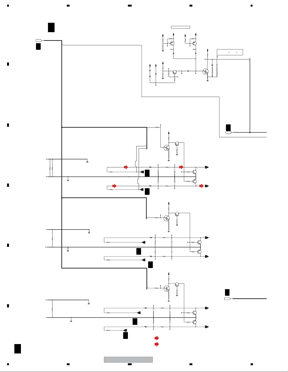
1234
3.4 DVDM ASSY (2/2)
B 2/2
DVDM ASSY (AWM8059)
A
from PAGE 1/2
AUDIO
ASPDIF
1/2B
V+6R5 V+5V
D852
D862 D861
V+12
R852
R853
GNDD
V+12
GNDD
R824 R823
10K
10K
15K
10K
VOLTAGE DETECT
V+5V
R851
47K
D851
Q821
2SA1576A(RS)
47K
R822
R821
Q851
2SA1576A(RS)
10k
VPR+8
V+12
R881
47K
10K
R882
D821
Q881
D881
Q801
DTC124EUA
V+3R3
2SA1576A(RS)
R801
GNDD
470
D801
UDZS4.7B
NORMAL : 3.3V
ABNORMAL : 0.5VDD
0.85VDD
0.1
C801
VDET
B
R517
1K
XAMUTE
DAC_SCK
DAC_SO
C
GNDD
R500 0
R590 0
GNDA
(DVDR)
R523
R524
0
0
(DVDL)
R919
AOUTL
AOUTR
B
C511
10/16
1/2B
C512
10/16
1/2
R511
R512
V+5V
Q505
1K
R518
2SA1576A(RS)
E
DTC114YUA
GNDD
R513
470
R514
470
GNDA
(DVDL)
C513
1000p
C514
1000p
C
B
R519
10K
Q501
2SD2114K(VW)
R515
2.2K
R516
2.2K
2SD2114K(VW)
Q502
(DVDR)
FL
FR
Q504
22K
22K
B
1/2
1-D6
to PAGE 1/2
SYS
D
E
F
24
B 2/2
V+5V
1K
Q535
Q534
R548
2SA1576A(RS)
E
C
DTC114YUA
R547
1K
XMMUTE
GNDD
R530 0
GNDA
GNDD
R560 0
GNDA
R553
0
Only
internal DAC 4ch
R554
0
R583
0
R584
0
B
B
AOUTSR
1/2
1/2B
AOUTSL
1/2
C541
10/16 470
AOUTCE
C542
10/16
AOUTSW
B
XMMUTE
C571
10/16
C572
10/16
(DVDL)
(DVDR)
R543
22K
R541
22K
R542
R544
470
1/2
R577
1K
R573
470
22K
R571
22K
R572
R574
470
: AUDIO SIGNAL ROUTE(DVD Lch)
: AUDIO SIGNAL ROUTE(DVD Rch)
GNDD
V+5V
Q564
DTC114YUA
GNDD
C573
C574
C543
C544
R578
1K
1000p
1000p
B
R549
GNDA
1000p 1000p
Q565
2SA1576A(RS)
E
C
B
R579
GNDA
10K
Q531
2SD2114K(VW)
R545
2.2K
R546
2.2K
2SD2114K(VW)
10K
Q561
2SD2114K(VW)
R575
2.2K
R576
2.2K
Q562
2SD2114K(VW)
Q532
CE
LFE
1/2
B
from PAGE 1/2
VIDEO
SL
SR
XV-EV9
1234
Page 25
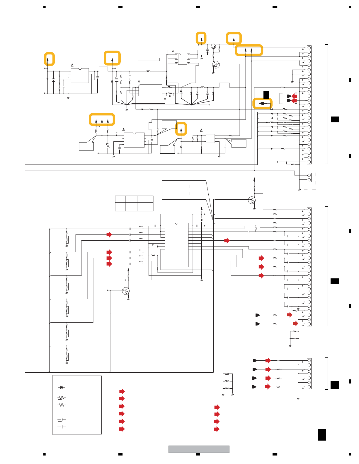
5678
V+1R8
C714
***
R_CR
C713
S_C
CVBS
S_Y
G_CY
B_CB
R714
2.2
R713R712
Chip Size
DIODE
RESISTOR
CAPACITOR
***
CH
C712
*** ***
GNDD
150F***
GNDD
*** 150F
R432 R412 R431 R411
GNDD
*** 150F
GNDD
150F***
GNDD
*** 150F
R435 R415 R434 R414 R433 R413
GNDD
150F
***
R436 R416
GNDD
V+12
2SA1576A(RS)
IC711
MM1661JH
1
2
NCVoNC
3
GND NC
4
Cn
Cont
470P
5.0V
1SS355
: 2125 Size
RS1/10S***J
: 1608 Size
(F):RS1/16S****F
OTHERS:RS1/16S***J
: 2125 Size
CKSQ**~
: 1608 Size
CH:CCSRCH~
OTHERS:CKSRYB~
Q732
RSQ035P03
V+3R3
8
Vin
7
6
C711
5
V+5S
L751
CTF1395
V+5V
10
1
V+5M
100/16
C739
0
R750
2.2
C753
GNDD
C738
R739
R404
R405
C752
*2
R738
R737
DCH1165
R736
0
CH
(C/V)
(Y)
(Cb)
(Cr)
Q401
DTC114YUA
VSEL1
(C/V)
(Cr)
(Y)
(Cb)
(USB+)
(USB-)
DC-DC CONVERTER D
L732
CH
ATH7011
C737
15K(F)
R735
27K(F)
18K(F)
GNDD
1
Vo Vin
2
NC
3
GND
4
Cn
470P
RGB
(BIAS) (CLAMP)
STBY
C411
C412
C413
C414
C415
C416
V+5V
R401
GNDD
22
120P
R1224N102H
2.7K
1
CE VIN
2
GND
3
VOUT EXT
47k
R734
D731
IC751
MM1565AF
75
Sub
Cont
5
IC731
6
R740
D732
RSX201L-30
5
R732
R733
4
0.1
C736
0
7.8V
0
R751
1
C751
6.4V
VSEL1 RGB V
R404
C403
*2
***
R405
10
11
12
13
14
*2
VSEL2 V+RGB S
1
Vcc1
2
C in
3
MUTE1
4
V in
5
YC MIX
6
Y in
7
GND1
8
BIAS
9
I/P
CY in
CLP
Cb in
MUTE2
Cr in
COMPONENT
1K
STBY
1K
0.1
1
1
C404
100/16
C405
0.1
1
0.1
0.1
10K
: VIDEO SIGNAL ROUTE
: VIDEO SIGNAL ROUTE
: VIDEO SIGNAL ROUTE
: VIDEO SIGNAL ROUTE
: DIGITAL SIGNAL ROUTE(BUS+)
: DIGITAL SIGNAL ROUTE(BUS-)
16
2
34
10
22
D733
C735
V+6R5
C761
IC401
MM1758XF
D
D
D
GS
10
DCH1165
100/16
Vcc2
DC out
C out
V out
GND2
Y out
CY out
GND2
Cb out
GND2
Cr out
GND2
5
C734
S1
S2
***:parts not mounted
C701
GNDD
L731
DTL1099
22
10
C733
C732
100/16
DCH1165
330k
330k
R763
R764
4
R762
V+5V
C401
C402
28
0.1
27
26
SQUEEZE
25
LETTER
24
23
22
21
20
19
18
17
16
15
GNDD
XV-EV9
56
Q701
1
GNDD
DCH1165
IC761
BA3948FP
39k(F)
100/16
I/XP
(SW)
(C)
(SL)
(SR)
VDVD+12
VPR+8
Q481
DTC114YUA
C406
0.1
(Cb)
(Cr)
CE
LFE
SL
SR
VPR+8M
V+5DVDPOWER
V+5V
1K
R481
GNDD
R402
(Y)
FL
FR
(SW)
(SL)
(SR)
XDVDRST
XREADY
SCLK
SDATA
MDATA
ACK
VDET
10K
(C)
L901
CTF1334
R921
R922
R923
R924
R403
R421
R422
R423
R424
R425
R426
R521
R522
R551
R552
R581
R582
R901
1/2B
R912
(DVDL)
R702
10
R701
10K
DTC124EUA
***
C731
1
2
3
GNDM
I/XP
SQUEEZE
VSEL2
VSEL1
(C/V)
GNDD GNDD
47K
Q702
R761
0
7.8V
1
C762
R1001
0
R1002
0
R1003
0
: AUDIO SIGNAL ROUTE(SUBWOOFER)
: AUDIO SIGNAL ROUTE(CENTER)
: AUDIO SIGNAL ROUTE(SURRUND Lch)
: AUDIO SIGNAL ROUTE(SURRUND Rch)
7
USBN
USBP
R902
0
R903
3.3k
R905
3.3k
R907
470
R908
3.3k
R910
220
R911
220
0
0
0
0
0
0
0
0
0
0
0
0
(DVDR)
0
0
0
0
0
GNDM
0
(USB-)
(USB+)
0
R915
C421
***
C422
***
C423
***
C424
***
C425
***
C426
***
C474
***
C475
***
C476
***
GNDD
R550
STBY
R557
STBY
R510
STBY
R904
6.8k
R906
6.8k
R916
R909
6.8k
R917
22K
22k
***
GNDA
GNDD
GNDD
27
26
25
24
23
22
21
20
19
18
17
16
15
14
13
12
11
10
9
8
7
6
5
4
3
2
1
CN901
VKN1319
1
2
CN952
STBY
CN902
VKN1319
1
2
3
4
5
6
7
8
9
10
11
12
13
14
15
16
17
18
19
20
21
22
23
24
25
26
27
CN903
VKN1299
1
2
3
4
5
6
7
VDVD+12
VPR+8/3R3V
VPR+8/3R3V
VPR+8M/6R5V
VPR+8M/6R5V
GNDM
GNDM
GNDD
GNDD
DOUT
GNDD
USBN
USBP
GNDD
V+5/DVDPOWER
XDVDRST
XREADY
SCLK
SDATA
MDATA
ACK
GNDD
GNDD
VDET
DVDMUTE
TRKUP
NC
P/XI
SQUEEZE
VSEL2
VSEL1
ASPECT
SC
GNDD
V
GNDD
SY
GNDD
CY/G
GNDD
Cb/B
GNDD
Cr/R
GNDD
R
GNDD
G
GNDD
B
GNDD
GNDA
FL
GNDA
FR
/ASDAT0
C
GNDA
/ACLK0
LFE
GNDA
/ABCK1
SL
GNDA
/ALRCK
SR
B 2/2
8
A
CN5502
1/3C
B
C
CN3001
D
2/3C
E
CN8002
D
F
25
Page 26
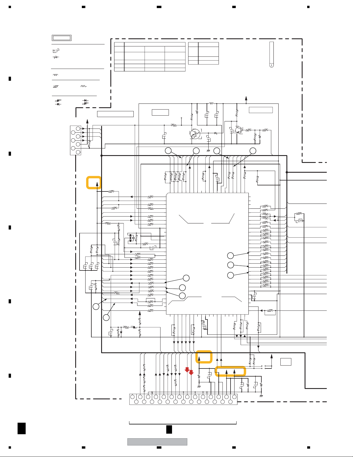
1234
3.5 MAIN ASSY (1/3)
A
B
NOTES
ALL CAPACITORS ARE IN µF
UNLESS OTHERWISE SPECIFIED
CH:CCSRCH*** Dest.
OTHER:CKSRYB***
TS:CE*****M##-TS
AL:CEAL***M##-*
(OTHER : CEAT***M##)
ALL INDUCTORS ARE IN µH
LAU***J
ALL RESISTORS ARE IN Ω
RS1/16
UDZS***
MTZJ***
FLASH E/D
FLASH DO
FLASH CLK
XRESET
VE+5
GNDU
CN5501
STBY
2
4
6
NC
RD1/4PU
ISS133
MA111
VE+5
VE+5
98
99
100
15k
R5615
1
3
5
7
C
10k
R5613
D
0.01
C5614C5626
C5613
C5612
0.022
0.01
2
E
SIMUKE
*
OTHERS
Unit
XWK3254-/J
No.
R5616
R5617
FLASH MICRO_P
R3704
100k
1
2
3
R5611
100k
5
6
7
R5616
**
R5617
ASS7034
C5619
0.01
1M
R5619
10k
R5612
17
18
19
20
0.01
22
23
24
1M
R5626
25
R5541
26
STBY
27
28
30
1
R5622
3.9k
R5623
180k
0.22
C5622
STBY
D5621
10k
X5601
10MHz
VD+5
D5620
MA111
DX / 6CH
DDXJ/RB
(M.EAST)
XWK3255-/J
39k
68kSTBY
RESET
220
R5501
1k
R5503
470
R5504
STBY
R5506
220
R5507
R5508
220
R5618
STBY
R5513
C5514
100
0.1
*
R5515
*
R5516
220
R5517
220
R5518
220
R5519
220
R5520
220
R5521
220
R5522
R5523
220
R5524
220
220
R5525
220
R5526
STBY
R5527
220
R5528
220
R5530
150k
R5620
10k
R5621
MODEL
RESET
Q5601
RT1N431M
STBY
470
R5597
979899
R5598
FLASH DO
FLASH E/D
(6CH)VOLDATA/CE
9
7
RYRC
MUSICLED
XRECMUTE
R5532
STBY
R5516
R5515
STBY
969495
R5596
(6CH)VOLCLK
1.DVDON/OFF
2.HPDET
3.MICDET
8
27.FLDATA
28.FLCLK
29.NC
30.XREADY
RYFS
*
Unit
No.
R5602
EXPWEM
MOVIELED
47k
C5602
3
XDVDRST
XSYSMUTE
NC
TIMERLED
R5537
STBY
XWK3254-/J
XWK3255-/J
XWK3256-/J
100/16
STBY
R5591
92
NC
IC5501
PDC139
VSS4
-
47k
C5603
STBY
C5604
GNDU
91
VDD4
C5539
MTXJ
(THAI)
XWK3256-/J
10k
10k
R5601
2.2K
YB
C5601
0.01
4
999697989495939091
100
STBY
STBY
R5600
R5599
100
FLASH CLK
45321
ACPULSE
(XMUTEC)
(RDSCLK)
REMOCON
XRESET
91011786
XT1
XT2
VSS1
CF1
1312 171514 16
CF2
VDD1
SIMUKE
MODEL
VDET
KEY1
KEY2
JOG
LEVELIN
XPROTECT
23 242221201918
SDATA
MDATA
SCLK
FLCS
29 3027 282625
NC
313433323536373938404142434445
DX
L5601
22u
9086879388
SYSPOW
FRTSURR
STBY
0.01
C5605
C5606
10/50
6
89
VDD3
UTEST-CHK
UTEST-EEPOK
0.1
STBY
VSS3
80.NC
79.NC
78.NC
STEST
C5588
ANDREWBYPASS
53.NC
52.TXCE
51.EESC
UTEST
10K
R5603
Q5602
2SC4081(QR)
CH
C5607
100p
8784868582
83
220
220
R5585
R5584
85
828381
84
MOVIE
XHPMUTE
2CHVOLCLK
2CHVOLDATA
TCMOTOR
ECHCNT-1
USBPOWER
TCXBEATCUT
TCPB/XREC
DVDMUTE
TCPULSE
DVDACK
TXIDATA
(RDSDATA)
12
(RDSPOW)
11
TXODATA
TCRECR
10
TCRECF
TCMODE
NC
NC
NC
EECS
4650474849
R5548
R5549
220
STBY
4.7k
MUSIC
XFLAG
TCBIAS
TCMSIN
TCSOL
TXCLK
TCHALF
VSS2
VDD2
EEDO
VE+5
R5604
1K
81
R5581
ECHCNT2
NC
EEDI
AC PULSE
R5606
10K
R5605
5
12K
R5556
78 777980
R5577
R5576
R5575
R5574
R5573
R5572
R5571
71 7073 727476 75
R5570
R5569
R5568
R5567
R5566
R5565
65 6466676869
R5564
R5563
R5562
R5561
R5560
R5559
R5558
58 575960616263
R5557
STBY
C5555
515254 5356 55
R5550
R5552
220
STBY
1K
1/50
C5608
SUBAC
220
8.2K
R5551
STBY
STBY
220
220
220
STBY
STBY
220
1K
STBY
220
STBY
STBY
STBY
STBY
STBY
STBY
STBY
STBY
STBY
VEF1040- X 2
77
75
74
73
72
71
70
69
68
67
66
65
64
63
62
61
60
59
58
57
94
5
MUTEC
MUTE
R5627
1M
C5627
0.01
F
26
C 1/3
U-COM
12345
VKN1258
CN5502
NC
NC(TRKUP)
69
R7012 R7011 R7021
VDET
DVDMUTE
17
00 0
68
GNDD
GNDD
SA
67
71711109
DVDACK
24
SDATA
MDATA
R7013
SCLK
302325
0
R7024
R7014
12
XREADY
XDVDRST
2/2B
1
93
0
(USB+)
0
151413 19
USBP
GNDD
DVDPOWER
CN901
36
D-
D+
GNDM(DV)
16
USBN
VPR+8M
(USB-)
C5621
XCH3021
GNDD
DOUT(NC)
C5620
1000/25
(Y)
20
GNDDV
GNDDV
0.1
21
22
GNDMDV
VPR+8
24272618
GNDMDV
VPR+8(M)
2523
VPR+8
VPR+8
VPR+8(M)
VP+12
0.1
C5623
VDVD+12
10k
R5543
C5624
47/16
C5625
52
10k
R5544
0.1
GNDD
VE+5
C5526
47/16
TEST
MODE
3233353437
XV-EV9
1234
Page 27
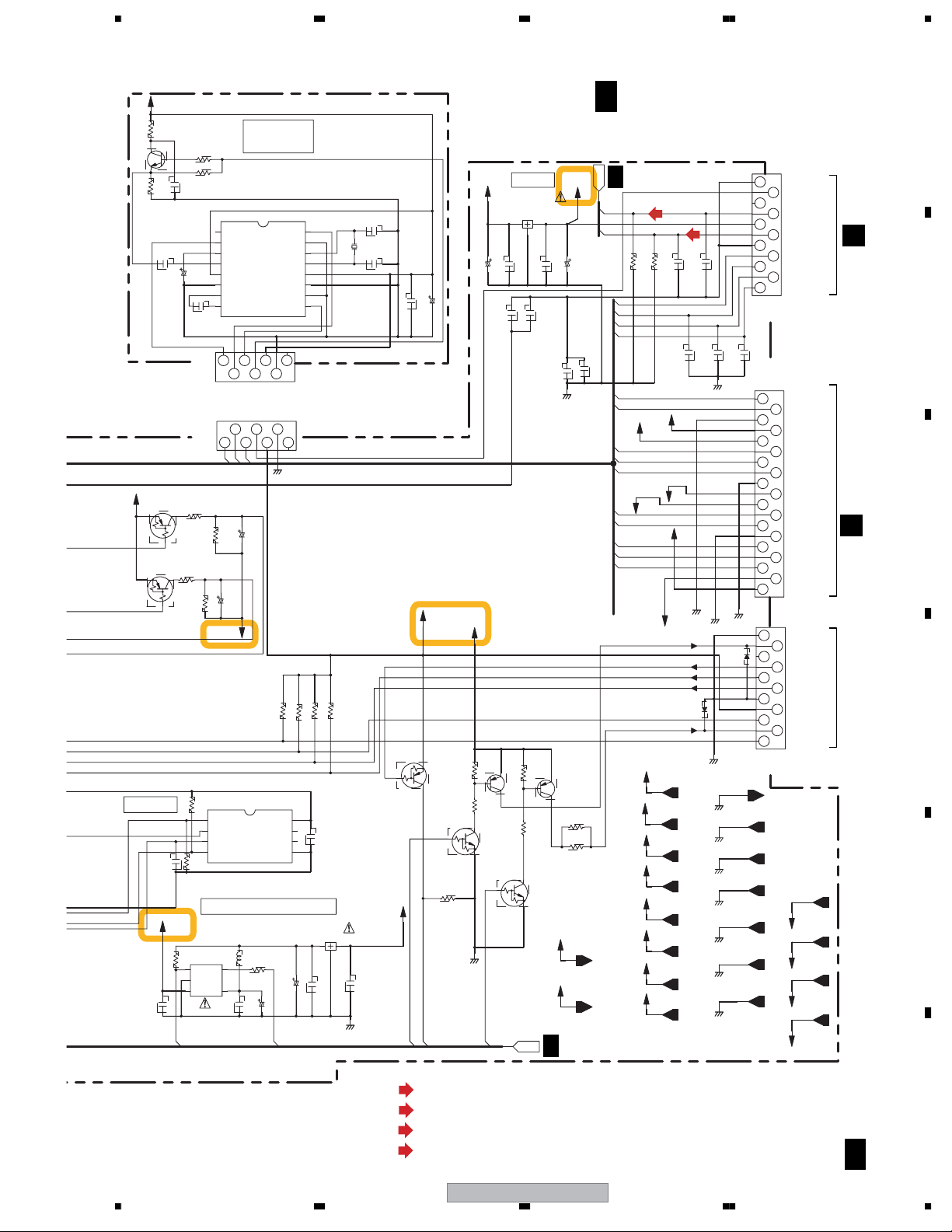
5678
VD+5
R5711
STBY
Q5712
STBY
STBY
R5713
C5712
STBY
VD+5
Q5603
RT1P431M
Q5604
STBY
BACKUP
V+5USB
C5901
0.1
STBY
RDS
FOR EURO MODEL
(LC72725M)STBY
IC5701
1
RDS-ID/READY
2
RDDA
3
VREF
4
MPXIN
5
VDDA
6
VSSA
7
FLOUT
8
CIN
2
STBYSTBY
RDSCLK
RDS DATA
CN5507 CN5506
47k
R5609
STBY
STBY
C5610
R5610
VA-12
IC5502
Main:
S-93C46BD0I-J8T1
Sub:BR93L46RFJ-W
47k
1
CS
27
SC
3
DI
4
DO
341
RDS
RDS POW
412
64656
22/25
C5609
5
53
6
VD+5
6
GNDD
Vcc
TEST
GND
RDCL
VDDD
VSSD
MODE
7
GNDD
7
R5813
NC
XOUT
TEST
47k
STBY
47p
C5554
CH
C5711
C5709
R5607
R5608
STBY
R5712
STBY
R5714
STBY
STBY
STBY
C5710
560
R5555
47k
R5554
USB POWER CONTROL
L5901
ATL7002-A-T
C5902
R5902
220
1
C5903
C5904
STBY
75
100k
R5901
34
2
15
IC5901
AAT4618IGV-0.5-1
74
RST
XIN
NC
8
6
5
10/50
47k
R5814
C5540
C5905
16
15
14
13
12
11
10
9
47k
R5816
R5815
0.1
IC5902
TA7805S
OUT IN
STBY
47k
GNDD
X5702
4.322MHz
C5906
C5714
STBY
C5713
STBY
STBY
0.047
VPR+8
CH
CH
C5715
RT1P241M
Q5803
63
STBY
C5708
VD+5
1k(1/4W)
RT1N431M
R5805
68
STBY
Q5802
47k
VM+12
R5801
R5802
GNDD
VA+12
NJM78M09DL1A-TLB
1/50
C5701
0.1
C5707
47k
Q5801
2SB1132(RS)
Q5805
RT1N431M
77
+9V REG.
IC5702
OUTIN
STBY
C5702
C5716
47k
R5806
R5807
1k(1/4W)
V+5USB
VA+9
U-COM
VA+9
0.1
C5703
C5704
STBY
0.01
C5717
GNDA
2SB1132(RS)
Q5804
R5808
R5809
V+5USB
VA+9
2/3,3/3
C
1
1
47/25
C5718
C
AUDIO
TXR
TXL
1000p
MAIN ASSY
1/3
(XWK3254:DDRXJ,DLXJ)
(XWK3255:DDXJ/RB)
(XWK3256:MTXJ)
STBY
C5720
D5802
STBY
CH
GNDLED
MA111
GNDU
11
9
7
5
3
1
CN5505
CKS3376
STBY
C5721
CH
CN5504
VKN1250
1
3
5
7
9
11
13
15
17
19
1
3
5
7
9
11
CN5503
CKS3376
GNDLED
1-C6
GNDM
(TC)
1-C6
GNDM
(DV)
GNDD
GNDA
GNDFL
66
61
62
52
37
7
20
19
18
36
33
27
28
26
VE+5
VFL+5
VPR+8
VPR+8M
VD+5
VA+12
VP+12
VM+12
2/3C
R5701
STBY
VE+5
FLAC2
R5702
VFL+5
VFDP
VPR+8M
(TXR)
STBY
FLAC1
VE+5
VFL+5
VPR+8
VD+5
VA+12
VP+12
VM+12
(TXL)
C5705
C5719
VP+12
STBY
C5706
STBY
CH
GNDU
GNDFL
MA111
D5801
GNDM(TC)
GNDU
GNDLED
GNDM
(TC)
GNDM
(DV)
GNDD
GNDA
GNDFL
GNDD
10
8
6
4
2
2
4
6
8
10
12
14
16
18
2
4
6
8
10
FLAC2
VA-12
GND
RDS
NC(VSM)
TXR
+9V
TXL
GND
DO
CLK
DI
CE
TIMERLED
REMOCON
GNDU
VP+12
VE+5
JOG
KEY2
KEY1
GNDLED
FLAC1
FLAC2
MOVIELED
MUSICLED
GNDFL
FLDATA
FLCLK
FLCS
VFDP
VFL+5
GNDM
SOL
NC
PULSE
HALF
MODE
GNDM(TC)
VD+5
RECF
MOTOR
RECR
FLAC1
VFDP
FLAC1
FLAC2
VFDP
VA-12
A
J
B
CN5301
C
E
D
TAPE DECK
MACHA CN8012
E
(TXL)
: AUDIO SIGNAL ROUTE(TUNER Lch)
(TXR)
(USB+)
: AUDIO SIGNAL ROUTE(TUNER Rch)
: AUDIO SIGNAL ROUTE(BUS+)
(USB-)
: AUDIO SIGNAL ROUTE(BUS-)
XV-EV9
56
F
C 1/3
27
7
8
Page 28
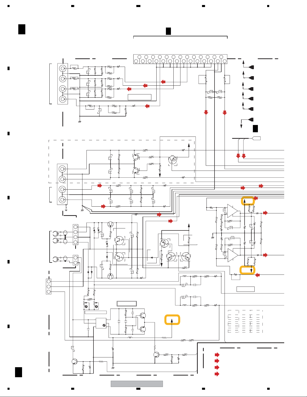
1234
3.6 MAIN ASSY (2/3)
A
B
C
D
E
F
28
C
2/3
C 2/3
MAIN ASSY
(XWK3254:DDRXJ,DLXJ)
(XWK3255:DDXJ/RB)
(XWK3256:MTXJ)
XKB3058
Q2806
L8871
2
STBY
4
5
L8861
STBY
3
L8851
STBY
1
6
GNDV
6
L
1
R
3
L
5
4
R
2
GNDC
CN2301
B4B-PH-K-S
4
Lch
3
GNDA
2
Rch
1
CN2302
B2B-PH-K-S
1
2
VR2802
C2809
(2125)
150p/200
ACG7058- -T
1-A4
GNDA
100k-B
PCP1032
C2808
4.7k
R2816
CH
47p
CH
47pCH
47p
D2302
BIAS OFFSET
8200p/100
STBY
STBY
R8876
C8872
STBY
STBY
R8866
C8862
C8852
R8856
STBY
STBY
L8821
STBY
C8822
(AUXL)
(AUXR)
D2301
MA111
MA111
D2303
D2304
1SS133
C2302
1SS133
1k
1k
R2814
R2813
R2804
STBY
61
52
4
L2801
RTD1082
HA
R2815
1k
(1/4W)
TS
C2810
33/50
VR2801
Cr
Cb
CY
V
JA8801
VIDEO/
COMPONENT+COMPOSITE OUTLINE IN
JA3002
AKB7015
LINE OUT
XKB3057
LINE IN
JA3001
YK56R-AA4N3
TAPE DECK
MECHA CN8011
321
STBY
CN2507
2SC2240(GR)
1%
R8875
1%
R8865
1%
R8855
CH47p
CH
C2301
10p
D2305
D2306
1SS133
10p
CH
100k-B
PCP1032
R8873
75
R8872
STBY
R8863
75
R8864
STBY
R8853
75
R8854
STBY
1%
C3001
C3002
220p
C3101
220p
C3102
Q2301
D
G
R2301
MA111
R2302
G
D
3
GND(TCB)
C8871
470/6.3
TS
C8861
470/6.3
TS
C8851
1000/6.3
R8821
75
R8823
STBY
R3001
STBY
STBY
R3002
R3101
15k
R3102
15k
2SK373(YGR)
S
STBY
Q2303
1M
DTC114TK
Q2304
DTC114TK
1M
Q2302
S
2SK373(YGR)
BIAS OSC.
C2801
0.012
C2805
33/50
R8822
STBY
Q3001
(1/2)
STBY
STBY
STBY
(2/2)
STBY
105KHz
R2802
M
C2802
R2801
LRCA151J
Q3001
STBY
C3103
STBY
C3104
C2304
10k
6800p
10k
L2802
0.15mH
NC(SQUEEZE)
NC(VSEL1)
NC(VSEL2)
NC(P/XI)
12345
VKN1258
CN3001
(Y)
VIDEO OUT
C8881
1000/6.3
STBY
R3003
STBY
R3004
STBY
R3103
R3104
C2305
(DECKL)
10/50
TS
C2303
820p
330k
R2303
330k
R2304
820p
C2306
TS
10/50
M
C2804
4700p
M
M
4700p
C2803
2SC1815(YGR)
Q2805
2SC1815(YGR)
NC(ASPECT)
NC(SC)
GNDD
V
6
(Cb)
(C/V)
R3005
STBY
R3006
STBY
R3007
22K
C3105
22K
C3106
10/50
(DECKR)
STBY
D2307
1SS133
VA-12
Q2801
2SC1815(YGR)
Q2802
VM
4.7
R2803
GNDD
STBY
VA-12
C3107
10/50
STBY
TS
STBY
C3108
RT1P241M
Q2351
R2805
160
(1/2W)
(1/2W)
R2811
1k
2/2B
NC(SY)
GNDD
GNDD
CY/G
12
1110987
13 17 21
(Cr)
Q3003
STBY
TS
RN1901
R2351
100k
Q2352
RN1901
(1/2)
CH
CH
VM+12
VM
47k
R2810
C2807
CN902
GNDD
GNDD
Cb/B
Cr/R
1614
15
VE+5
C3003
STBY
C3004
STBY
VA+12
R2352
Q2352
(2/2)
R7027
0
RTF1004
L2811
10mH
C2811 C2813
220p 1500p
C2812
220p
L2812 R2822
RTF1004
10mH
R7016 R7018
00
(BIAS)
R2809
1k
TS
47/25
(XBEATCUT)
GNDD
GNDD
NC(G)
NC(R)
NC(B)
181920 222324
STBY
R1501
C1509 C1510
STBYCHSTBY
CH
R1503 R1504
STBY STBY
(DVDL)
3110
STBY
GNDA
22k
STBY
R2821
R2823
11k
1k
M
C2814
M
1500p
R2824
1k
11k
73
72
(C/V)
(Cb)
GNDD
GNDA
GNDA
FR
FL
26
25 27
STBY
R1502
VA+12
VM+12
VA+9
VE+5
VD+5
(DVDR)
VA-12
TXR
(TXR)
(AUXR)
IC3110(1/2)
CH
47p
NJM4565MD
C3111
4
+
3
1
-
8
2
*
R3113
C3113
C3119
R3123
47p
CH
R3705
47/16
47/16
0
*
6
5
R3118
*
C3114
100p
CH
C3121
100p
CH
R3124
*
8
-
(2/2)
+
4
IC3110(2/2)
NJM4565MD
C3126
STBY
7
39k
R3112
39k
R3122
C2815
1/50
TS
C3120
HP AMP
C2816
1/50
TS
71
(PB/REC)
: VIDEO SIGNAL ROUTE
(Cr)
: VIDEO SIGNAL ROUTE
(Y)
: VIDEO SIGNAL ROUTE
R3114
R3115
R3118
R3124
R3126
R3131
R3113
R3123
3257-3259
82
82
33k 18K
33k
82
82
2.2K
2.2K01.2K
: VIDEO SIGNAL ROUTE
VA+12
VM+12
VA+9
VE+5
VD+5
VA-12
AUDIO
TXL
(TXL)
(AUXL)
VA+12
47
R3111
R3110
47/16
0.1
TS
C3116
STBY
C3115
0.1
TS
STBY
C3123
C3122
C3127
47/16
NP
47
R3129
R3130
VA-12
XWM XWM
3251-3256
X
0
18K
X
1.2K
47
C3112
NP
10/50
C3117
10/50
C3124
1/3C
(HPR)
(HPR)
TS
R3125
TS
(HPL)
47
(HPL)
100k
R3119
100k
XV-EV9
1234
Page 29
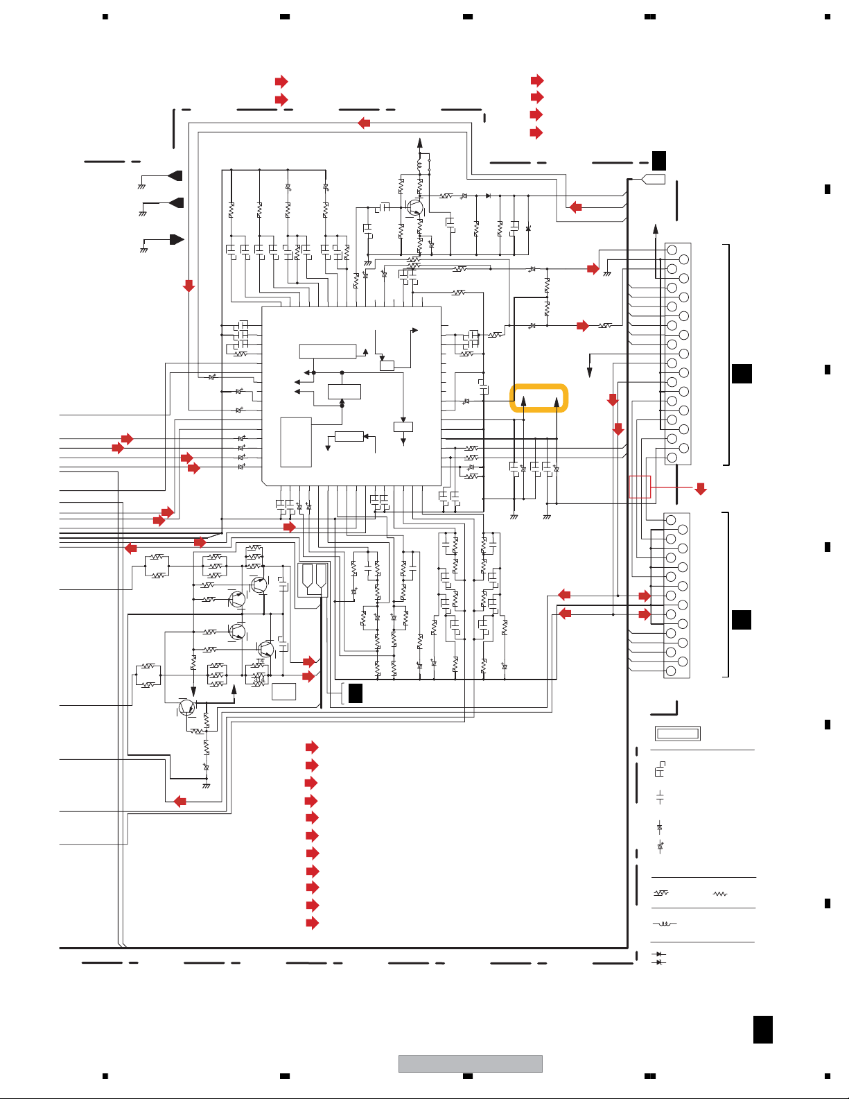
5678
GNDD
GND(TCB)
GNDA
(TXL)
(TXR)
(XRECMUTE)
32
(AUXL)
(AUXR)
(HPR)
R3126
R3131
2SA1576A(QR)
RECAC
GND(TCB)
R3114
*
R3115
*
*
*
GNDD
GNDA
(MIC)
Q3114
VA-12
1-C1
C3051
2200p
C3052
2200p
C3053
C3080
10/50
C3057
C3055
C3056
C3059
C3060
(DVDL)
(DVDR)
(DECKR)
R3120
2.2k
R3121
2.2k
R3127
R3128
47k
R3133
R3135
R3136
1k
GNDD
(HPL)
1
TS
R3146
R3144
2.2k
2.2k
R3140
R3139
R3138
R3137
100
IMX9-T
Q3110
15k
1k
C3128
R3044
0.1
C3050
R3051
4.7k
C3054
0.33/50
TS
10/50
10/50
10/50
10/50
10/50
IC3001
BD3401KS2
C3011
STBY
R3145
100
100
100
Q3110
(2/2)
100
100
VD+5
10/50
4.7K
1
C3048
TS
TS
TS
TS
C3012
STBY
(DECKL)
100
100
100
Q3111
(1/2)
IMX9-T
Q3111
IMX9-T
(2/2)
R3141
R3142
R3143
(FL)
(FR)
R3043
1
C3047
TNF2
TNF1
SUR1
SUR2
LINEOUT2
LINEOUT1
SAOUT2
SAOUT1
CAP
MIC
A1
A2
B1
B2
C1
64 62 6163 5960 58 57 5556 5354 52 51 50 49
C2
C3013
10/50
R3149
R3148
R3147
(1/2)
(XHPMUTE)86
: AUDIO SIGNAL ROUTE(Lch)
: AUDIO SIGNAL ROUTE(Rch)
(MIC)
TS
C3045
10/50
R3041
4.7K
C3029
STBY
0.1
C3049
474846454443424140393836353734
MNF2
INPUT Buffer
SEL
D1
124537689
10/50
C3014
C3118
1000p
1000p
100
C3125
100
100
HP
MUTE
(DVDL)
(DVDR)
(DECKL)
(DECKR)
(TXL)
(TXR)
(HPL)
(HPR)
(AUXL)
(AUXR)
(MIC)
TS
C3046
4.7K
0
R3029
MOUT2
MOUT1
SURROUND
RECAC
(HPR)
(HPL)
C3043
MNF1
E2E1D2
AUDIO
10/50
R3042
C3044
0.068
BNF1
PBNF2
0.068
BOUT1
BASS/TRE
MIC MIX
KARAOKE
PBOUT2
U-COM
4.7K
STBY
C3030
BOUT2
PBOUT1
0
R3030
10k
R2101
BNF2
PBNF1
680
R2312
C2326
R2354
C2101
0.01
C2102
GNDU
C3042
10/50
AMSOUT
TONEOUT2
TAPEA1
TAPEA2
11101214131615
STBY
C3015
MB
6800p
C2322
R2324
3.3/50
0
C2324
R2326
R2328
1/3,3/3C
1800p
C3041
10/50
R7028
R70290 0
VIN2
TONEOUT1
VOL
TAPEB1
TAPEB2
470K
R2322
33K
STBY
C2323
0
STBY
R2327
: AUDIO SIGNAL ROUTE(DVD Lch)
: AUDIO SIGNAL ROUTE(DVD Rch)
: AUDIO SIGNAL ROUTE(TAPE Lch)
: AUDIO SIGNAL ROUTE(TAPE Rch)
: AUDIO SIGNAL ROUTE(TUNER Lch)
: AUDIO SIGNAL ROUTE(TUNER Rch)
: AUDIO SIGNAL ROUTE(HEADPHONE Lch)
: AUDIO SIGNAL ROUTE(HEADPHONE Rch)
: AUDIO SIGNAL ROUTE(LINE Lch)
: AUDIO SIGNAL ROUTE(LINE Rch)
: AUDIO SIGNAL ROUTE(MICROPHONE)
R2102
R2105
VIN1
BBIN1
BBNF1
ALC
RECNF2
STBY
C3016
470K
R2321
R2323
STBY
R2325
STBY
VA+12
L2101
STBY
120k
R2103
33k
R2106R2104
C3031
33
VOLOUT2
BBNF2
BBIN2
VOLOUT1
SWOUT
FILTER
1/2VCC
VCC
GND
VDD
ALC
RECOUT2
RECNF1
RECOUT1
MB
6800p
C2321
33K
0
R2353
0
R2311
TS
C2325
3.3/50
R2107
3.9k
Q2101
2SC4081
270
1k
STBY
C3033
LF1
LF2
LF3
LF4
SI
SC
C3017
C2402
C2404
C2406
R2408
680
W288
1k
C2104
C2103
22/50
STBY
STBY
0.033
STBY
220p
68K
TS
C2410
3029 31 32
17 1918 20 2221 2423 2625 2827
MB
10/50
TS
R3031
R3033
STBY
C2408
R2410
C2105 D2101
10/50 1SS133
TS
STBY
R2108
100k
STBY
C3032
STBY
R3034
STBY
C3034
STBY
R3032
STBY
C3024
47/25
TS
R3013
220
220R3012
C3019
4.7/50
TS
R3011
4.7M
STBY
C3018
220K
220K
R2402
R2401
470K
R2404
R2403
STBY
R2406
220p
C2407
4.7K
R2409
R2109
C3027
MB
470K
220p
4.7K
470p
GNDA
C2401
R2407
(SW)
: AUDIO SIGNAL ROUTE(SUBWOOFER)
(C)
: AUDIO SIGNAL ROUTE(CENTER)
(SL)
: AUDIO SIGNAL ROUTE(SURRUND Lch)
(SR)
: AUDIO SIGNAL ROUTE(SURRUND Rch)
U-COM
70
(MIC)
MIC
0.33
270k
C2106
10/50
VA+9
C3035
10/50
TS
C3036
TS
STBY
D2102
VD+5
47k
R3039
47k
R3040
(6CH)
(FL)
(FR)
VA-12
R3702
(FL)
GNDA
0
SA
VA+12
CN3004
XKM3006
95
96
97
90
82
83
87
(FR)
84
TS
470p
C3020
0.033
STBY
C2403
STBY
R2405
68K
C2405
C2409
10/50
TS
47/25
C3021
220p
TS
0.1
C3025
GNDD
C3022
1000p
C3023
47/25
(HPR)
(HPL)
(6CH)
85
(FR)
(FL)
MUTE
MUTEC
35
34
22
CN3003
NOTES
ALL CAPACITORS ARE IN µF
UNLESS OTHERWISE SPECIFIED
ALL RESISTORS ARE IN Ω
UNLESS OTHERWISE SPECIFIED
ALL COILS ARE IN µH
UNLESS OTHERWISE SPECIFIED
ALL DIODES ARE 1SS133
UNLESS OTHERWISE SPECIFIED
1/3,3/3C
FL
GNDA
FR
3
VA+12
4
EXPWRM
51
6 2
E-CLK
7
E-DATA
8
FRTSURR
MUSIC
MOVIE
ABYPASS
11 9
VA-12
12
FLIN
13
GNDA
FRIN
GNDA
16 14
CIN
17 15
GNDA
18 10
SWIN
19
GNDA
20
SLIN
GNDD
22
SRIN
23 21
(SW)(C)
(SL)(SR)
SRIN
16
GNDA
1517
SLIN
14
GNDA
13
SWIN
12
GNDA
CIN
10
GNDA
FRIN
GNDA
711 9
FLIN
68
GNDA
MUTE
4
MUTEC
35
RYFS
2
RYRC
1
XPROT
CKS3382
CH:CCSRCH***
YF:CKSRYF***
OTHER:CKSRYB***
M:CQMA***
HA:CQHA***
MB:CQMBA***
CEANPR**M##-T
TS:CE*****M##-TS
JQ:CEJQ***M##-*
AL:CEAL***M##-*
(OTHER : CEAT***M##)
1/16W
LAU***J
1SS133
MTZJ***
A
B
CN8001
D
C
CN3031
H
D
E
1/4WPU
56
XV-EV9
F
C 2/3
29
7
8
Page 30
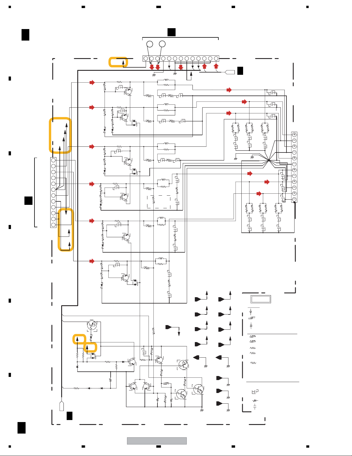
1234
3.7 MAIN ASSY (3/3)
C
A
B
C
D
E
F
MAIN ASSY
3/3
(XWK3254:DDRXJ,DLXJ)
(XWK3255:DDXJ/RB)
(XWK3256:MTXJ)
VD+5
VP+12
VM+12
VA+12
SROUT
12
VD+5
11
SLOUT
10
9
VA-12
COUT
8
VP+12
SWOUT
VFL+5
FROUT
VPR+8
VPR+8
FLOUT
CN3302
52147-1210
7
6
5
4
3
VA-12
2
1
VPR+8
VFL+5
22
RECAC
RT1P241M
22k
R3631
D3631
R3635
3.3k
AC1
(1/4W)
U-COM
1-D6
1/3,2/3C
J3032
H
(FL)
(FR)
(SW)
(C)
(SR)
(SL)
Q3635
VH+
22k
R3632
(1/4W)
MTZJ5R1B
D3632
1SS133
D3636
VD+5
(1/4W)
MA111
D3635
DAN202K
1.8k
R3612
33k
MA111
D3622 R3624
R8880
R3614
D3612
D3633
1SS133
R3601
33k
R3603
D3601
1.8k
R3621
R3623
D3621
MA111
1.8k
33k
MA111
R3611
R3613
D3611
1.8k
MA111
33k
1.8k
33k
MA111
(XPROT.)
R3633
6.8k
1/4W
C3672
ACN7112(2W)
2SC4081(QR)
ACN7112(2W)
C3631
V+5USB
R3607
0.1
ACN7112(2W)
STBY
B
Q3601
2SC4081(QR)
R3608
0.1
ACN7112(2W)
1.8k
R3602
B
33k
R3604
Q3603
2SC4081(QR)
MA111
D3602
0.1
R3627
ACN7112(2W)
C3627
STBY
B
Q3621
2SC4081(QR)
D3623
DAP202K
0.1
R3628
C3675
STBY
B
Q3622
0.1
R3618
ACN7112(2W)
C3677
STBY
B
Q3612
2SC4081(QR)
R3617
0.1
C3676
STBY
B
Q3611
2SC4081(QR)
2SC4081(QR)
D3634
1SS133 (1/4W)
1/4W
2.7k
R3634
TS
2.2/100
Q3637
2SC4081(QR)
E
C
C3673
STBY
E
D3603
DAP202K
C
E
C
E
C
E
C
E
C
D3613
DAP202K
Q3631
J5401
F
13
14
D+
V+5USB
D-
(USB-)
GNDD
R7005
(1/2W)PMF
(1/2W)PMF
R7006
22k
R3669
ATH-059
R3361
(1/2W)PMF
C3361
0.022
L3362
C3362
0.022
L3561
R3561
(1/2W)PMF
C3561
0.022
L3661
ATH-059
R3461
(1/2W)PMF
100
0
2ch &
6ch
L3461
ATH-059
R8883
100
L3462
ATH-059
R3462
100
0
R3017
Q3638
C3632
470/6.3
GNDD
(USB+)
L3361
VA-12
Q3639
2SA1576A(QR)
R3651
STBY
R3638
1234567 9108111213
CN3301
52147-1310
R3605
27k
R3606
27k
R3625
27k
R3626
27k
R3616
27k
R3615
27k
C3668
0.01
R3668
22k
2SC4081(QR)
3
100
R3363
4.7
ATH-059
R3364
4.7
ATH-059
100
R3563
4.7
C3461
R3463
C3463
0
10k
MIC SW
GNDA
(MIC)
GNDA
C3363
0.022
R3362
(1/2W)PMF
0.022
C3563
0.022
C3562
R3562
C3564
C3462
R3464
C3464
0.022
4.7
0.022
VA-12
Q3632
RT1P241M
C3633
10/50
TS
C3364
0.022
4.7
0.022
0.022
4.7
0.022
R3639
MIC
VA+12
100
27k
Q3640
RT1N241M
VA+12
HPDET
ECHOVOL
81
2
VFL+5
V+5USB
RETGND
RETGND GNDREG
Q3633
RT1N431M
GNDB
HPR
HPL
GNDA
AUDIO
(HPL)
(HPR)
(FL)
(SW)
R3565
STBY
RETGND
VD+5
VP+12VD+5
VM+12 VA+12
VA+12VM+12
VFL+5
VPR+8
V+5USB
VH+
GNDREG
GNDA
GNDA
GNDB
GNDB
GNDD
GNDD
2/3C
(FR)
XCG3008
(1/10W)
(1/10W)
(1/10W)
STBY
R3566
R3366
STBY
(1/10W)
C3366
STBY
STBY
C3565
STBY
STBY
C3368
C3567
GNDREG
(C)
(SL)
STBY
(1/10W)
R3466
R3468
C3468 C3466
STBY STBY
NOTES
DIODE
VPR+8
ALL RESISTORS ARE IN Ω
VH+
(1/10W)
PMF(1/2W)
VM
ALL CAPACITORS ARE IN µF
UNLESS OTHERWISE SPECIFIED
XCG3008
(1/10W)
R3368
R3365
STBY
STBY
C3365
C3367
SP CHASSIS
(SR)
STBY
STBY
(1/10W)
(1/10W)
STBY
R3467
R3465
C3465
C3467
1SS133
MA 111
MTZJ***
RS1/16S***J
RS1/10S***J
RD1/4PU***J
RD1/2PMF***J
RD1/2VM***J
CH:CCSRCH
(OTHER: CKSRYB)
CEAT
M:CQMA
C3369
C3370
XCG3008
C3569
0.01
STBY
R3367
STBY STBY
C3669
0.01
XCG3008
C3470
0.01
XCG3008
C3469
0.01
XCG3008
(1/10W)
(1/10W)
STBY
STBY
0.01
0.01
(1/10W)
R3665
C3665
C3667
STBY
STBY
STBY
JA3301
XKE3037
STBY
R3667
(1/10W)
XKE3051
JA3301
FR
FL
SW
C
SR
SL
(12 PINS)
C 3/3
30
XV-EV9
1234
Page 31

5678
(USB+)
: DIGITAL SIGNAL ROUTE(BUS+)
(USB-)
: DIGITAL SIGNAL ROUTE(BUS-)
*
C16
(T1)
TRANSFORMER
CN3
G
VFDP Protect Circuit
CQMA333K2E
VFDP
BHAC1
BLAC1
GND
BLAC2
BHAC2
SUBAC1
SUBAC2
FLAC1
FLAC2
SYSPOW
GNDU
SUBAC
VE+5
XPROT
D20PYY0525E
XWM
3257-3259
CN11
B10PS-VH
1
2
3
4
5
6
7
8
9
10
1
2
3
4
5
J12
51048-0500
GNDU
RETGND
GNDREG
XWM
3251-3256
CQMA473K2E
C31
STBY
VE+5
GNDU
GNDU
RETGND
GNDREG
C35
D13
STBY
D14
S5688G
S5688G
VH+
VL+
UN+8V
VE+5
C22
C21
220/63
R12
PMF
Q11
2SB1565(EF)
R17
82k
R18
220k
VH+
VL+
UN+8V
VE+5
(MIC)
: AUDIO SIGNAL ROUTE(MICROPHONE)
CAUTION : FOR CONTINUED PROTECTION AGAINST
RISK OF FIRE. REPLACE ONLY WITH
SAME TYPE NO. 491007 MFD, BY
LITTELFUSE INK. FOR IC15 (AEK7021).
D11
-
C15
STBY
24V
C19
4700/35
-24V
VL-
C33
GNDD
GNDM(DV)
GND(TCB)
FLAC2
91
22
GNDM(DV)
GND(TCB)
~
~
GNDS
D5SBA20(B)
+
2200/63
XCH3024
XCH3024
C30
STBY
STBY
SCREW:BBZ30P080FNI
HT SINK:XNH3030
D5SBA20(B)
C17
M
*
C16
C18
D15
MTZJ33B
33/50
C23
D800
STBY
22/50
3.9k
D16
1SS133
(1/2W)
GNDFL
VFDP
Q13
RT1N241M
VA-12
FLAC1 VH-
FLAC2
VFDP
VA-12
C14
C13
STBY
R13
D12
~
C26
-
+
STBY
STBY
STBY
VDFP
VA-12
~
C27
C28
STBY
STBY
R11
STBY
STBY
C32
STBY
-
C24
6800/25
IC15
(7A)
AEK7021-
C34
5.6k
10/50
(1/4W)
R15
D18 R14
100
(1/4W)
MTZJ4.3B
Q12
RT1P241M
FLAC1 VH-
FLAC2
VL-
GNDD
GNDFL
STBY
STBY
VL+ 2200/63
C29
STBY
4700/35
C20
D17
D5SBA20(B)
~
+
~
C25
100
R16
(1/4W)
FLAC1
SUBAC
VL-
GNDD
GNDFL
VH+
C11
C12
GNDM(TC)
GNDB
GNDDV
GNDS
GNDM(DV)
GND(TCB)
HT SINK:STBY
44V
C8883
C8882
VH-
GNDLED
IC16
GNDP
GNDDV
GNDB
GNDM(TC)
CAUTION : FOR CONTINUED PROTECTION AGAINST
RISK OF FIRE. REPLACE ONLY WITH
SAME TYPE NO. 491007 MFD, BY
LITTELFUSE INK. FOR IC16 (AEK7047).
SCREW:STBY
STBY
-44V
STBY
RETGND
GNDS
UN+8V
15V
GNDREG
(7A)
AEK7047
AC1
GNDDV
(SECONDARY)
GNDB
GNDM(TC) GNDP
1/3C
U-COM
MAIN ASSY
GNDLED
GNDLED
GNDP
CN13
52147-1510
1
2
3
4
5
6
7
8
9
10
11
12
13
14
15
1-D1
VH+
VH+
GNDF
UN+8V
UN+8V
GNDREG
VL+
VL+
GNDP
GNDP
GNDS
VL-
VL-
VH-
VH-
A
B
C
D
J3033
H
E
(FL)
: AUDIO SIGNAL ROUTE(Lch)
(FR)
: AUDIO SIGNAL ROUTE(Rch)
(SW)
: AUDIO SIGNAL ROUTE(SUBWOOFER)
(C)
: AUDIO SIGNAL ROUTE(CENTER)
56
(SL)
: AUDIO SIGNAL ROUTE(SURRUND Lch)
(SR)
: AUDIO SIGNAL ROUTE(SURRUND Rch)
(HPL)
: AUDIO SIGNAL ROUTE(HEADPHONE Lch)
(HPR)
: AUDIO SIGNAL ROUTE(HEADPHONE Rch)
XV-EV9
7
F
C 3/3
31
8
Page 32

1234
3.8 EVOL ASSY
R8102
STBY
A
CN8002
VKN1238
1
C
2
GNDA
GNDA
GNDA
SW
SL
64
SR
R8101
R8105
53
7
R8106
CN903
B
2/2B
C
D
E
NOTES
F
(FR)
95
GNDA
ALL CAPACITORS ARE IN µF
UNLESS OTHERWISE SPECIFIED
ALL RESISTORS ARE IN Ω
D
32
1234
STBY
C8102
STBY
C8101
STBY
STBY
STBY
C8103
C8104
STBY
STBY
FC:50kHz
(FL)
(SL)
(SR)
(C)
(SW)
UMBIN(1/2)
E
Q8202
RT1N241M
RS1/16S***J
RD1/2VM***J
VA+12
R8103 R8104
STBY STBY
STBY
R8107
STBY
R8108
R8204
820
C8204
C8203
R8203
820
EXTRA POWER
R8205
820
C8205
3900p
C8206
3900p
R8206
820
R8207
820
C8208
Q8201
BCE
B
E2
Q8201
UMBIN(1/2)
CH : CCSRCH
AL : CEAL
TL : CFTLA
R8264
STBY
R8266
3900p
*
3900p
MODE
VA+7
141312111098
IC8402
HEF4066BT
1235467
3900p
141311128109
IC8403
HEF4066BT
1
B2
C2
(FR)
(OTHER : CKSRYB)
(OTHER:CEAT)
VA+12
R8269
R8267
STBY
C9001
*
R8265
(SR)
(C)
2C35476
R8201
6.8k
R8202
10k
ALL DIODE
:MA111
R9002
STBY
*
STBY
R9001
STBY
C9002
R8268
STBY
*
C8201
VA-12
DWNMIXR
DWNMIXL
C8210
0.1
C8207
0.1
C8209
C8202
(SW)
R8210
(SW)
(FL)
VA-12
0.33
12k
2.2k
R8211
C8213
3.3/50
(SL)
(FR)
0.1 0.1
XV-EV9
R8212
4.7k
R8260
10k
2.2k
R8213
R8214
2.2k
R8215
6.8k
C8216
10/50
C8217
10/50
C8215
10/50
R8501
10k
C8501
STBY
R8502
4.7k
R8504
4.7k
C8502
STBY
R8506
10k
C8517
STBY
C8518
STBY
VA+12
VA-12
CN8001
XKP3055
GNDA
R8261
1.8k
R8208
39k
C8212
3300p
R8216
C8211
10/50
1k
R8263
18k
C8214
10/50
R8209
39k
(SR)
(C)
(FL)
R8507 R8511
10k
2
8
1
IC8405
(1/2)
3
+
NJM4565MD
4
3.3k
R8503
5
IC8405
(2/2)
6
R8509
10k
R8518
+
-
R8521
22
NJM4565MD
4
7
8
22
3.3k
R8505
(SL)
STBY
R8523
R8524
STBY
(SR)
1357
24 86
FL
FR
GNDA
VA+12
GNDA
1
INP1
2
INN1
3
OUT1
4
R8262
1.8k
GND
5
INP2
6
INN2
7
OUT2 DGND
8
GND
9
SWIN
10
GND
11
SRIN
12
GND
13
SLIN
14
GND
15
CIN
16
GND
17
FRIN
18
GND
19
20
(SL)
3.9k
NJM4565MD
R8508
1.8k
2
IC8406
(1/2)
3
STBY
C8503
0.1
C8512
5
0.1
C8515
6
C8504
STBY
R8516
3.9k
IC8406
(2/2)
R8510
1.8k
NJM4565MD
FRONT SURROUND
141213111098
IC8404
HEF4066BT
231
456
97
969587
91113151719202321
10
E-CLK
MUSIC
E-DATA
EXPWRM
FRTSURR
GNDD
E-VOL
IC8401
8
+
4
4
+
-
8
C8516
12
MOVIE
ABYPASS
BD3814FV
VCC(+7V)
SWOUT
SROUT
SLOUT
FROUT
FLOUT
BNF2R
BNF1R
C8505
1
0.1
C8511
0.1
C8513
7
0.1
(SR)
7
RT1P241M
14 16 18
FLIN
VA-12
GND
GND
CLK
DATA
MUTE
GND
COUT
BNF2L
BNF1L
TNFLFLIN
TNFRVEE(-7V)
STBY
C8506
Q8305
FRIN
GNDA
GNDD
40
39
38
37
36
35
34
33
32
31
30
29
28
27
26
25
24
23
22
21
C8226
+
3
IC8407
(1/2)
-
2
R8512
10k
0.1
C8514
R8514
10k
6
-
IC8407
(2/2)
5
+
STBY
NJM4565MD
R8303
C8519
0.1 0.1
C8520
R8304
CIN
GNDA
R8217
(C)
(FL)
0.1
0.1
0.1
0.1
STBY
(SR)
4
NJM4565MD
1
C8508
8
3300p
R8513
10k
C8507
3900p
C8509
3900p
R8515
10k
C8510
3300p
8
7
4
(SL)
6.8k
10k
Q8306 Q8303
RT1P241M
SWIN
GNDA
GNDA
96
97
1k
1k
R8218
C8218
100p
CH
C8219
100p CH
R8219
1k
(SW)
(FR)
R8220
4.7k
C8220
C8221
C8222 R8221
4.7k
C8223
C8224
4700p
C8225
4700p
GNDD
VA+12
150
R8001
UDZS6R8B
D8001
D8002
UDZS6R8B
150
R8002
VA-12 VA-7
(SL)
UMBIN(2/2)
Q8303
UMBIN(2/2)
22
SLIN
SRIN
GNDD
CN3004
VA+7
1/2W VM
220/10
C8001
C8002
220/10
1/2W VM
RT1N241M
(SR)
Q8307
RT1P241M
2/3C
TS
C8004 C8003
TS
Q8304
0.1
0.1
Page 33

5678
87
C8601
STBY
C8613
STBY
(FR)
VA-12
VA+12
NJM4565MD
R8707
6.8k
R8708
2SK303(34)
Q8701
1M
R8719
MA111
D8703
MUSIC
(SW)
C8701
STBY
SW LPF
SW fc=200Hz
R8268 4.7K
R8265
R8266
R8267 3.3K
R8604 3.3k
R8618
R8625
R8637
R8621 10k
R8631
R8622
R8633
R8627
R8640
R8628
R8641
R8724
R8634
R8665 STBY
R8666
R8725 10k
R8636
(FL)
D8601
MA111
1M
R8664
10k
R8709
4.7k
G
0.33
C8745
1M
R8721
R8701
STBY
C8702
XWM
3251-3253
4.7K
3.3K
3.3k
2.2k
2.2k
10k
22k
22k
120k
120k
2.2k
2.2k
0
0
STBY
10k
S
D
100
R8711
STBY
C8712
TL
STBY
R8702
2SK303(34)
R8601
R8602
2SK303(34)
+
3
IC8502
(1/2)
-
2
R8710
2SK303(34)
C8744
0.33
C8713
STBY
TL
560
R8713
R8714
(SL)
10k
0.1
C8703
XWM
3254-3256
0
0
STBY
STBY
2.7k
2.7k
X
X
47k
47k
2.7k
2.7k
X
X
2.2k
2.2k
6.8k
6.8k
0
0
0
0
6CH
R8603
Q8501
S
1M
1M
Q8502
S
4
1
8
4.7k
Q8702
Q8401
2SC4081(QR)
C8715
STBY
C8746
0.68
100k
R8715
SW XBOOM
STBY
STBY
C8704
C8705
47K
G
G
47k
R8617
C8614
22
R8706
100
R8712
STBY
C8714
R8716
10k
0.082
C8706
(FL)(FR)
(SW)(C)
(SL)(SR)
C8605
C8609
S
R8705
D
TL
180
R8703
D
*
*
D
22
TL
(SR)
R8704
220k
C8605
C8606
C8609
C8610
C8632
C8633
R8618
*
0.1
0.1
C8710 C8711
G
C8747
82k
TY
STBY
C8707
C8602
C8614
C8617
C8618
C8621
C8625
C8626
C8628
C8602
*
R8604
*
*
0.68
R8717
C8709
R8605
R8611
100k
STBY
(1/2)
STBY
C8603
STBY
STBY
R8606
R8607
R8613
STBY
STBY
R8612
STBY
C8615
NJM4565MD
(SW)
MOVIE
Q8402
2SC4081(QR)
10k
R8718
1M
R8722
IC8502
NJM4565MD
6
-
5
+
+13.4dB
XWM
3251-3253
3300p
0.022
3300p
0.022
3300p
3300p
0.33
0.33
3300p
0.015
STBY
3300p
0.015
STBY
IC8501
NJM4565MD
+
3
+14.4dB
-
2
R8608
2.2k
2.2k
R8614
6
-
+14.4dB
5
+
(2/2)
1M
R8720
MA111
D8704
C8708
820p
(2/2)
8
7
4
3254-3256
5600p
0.027
4700p
0.027
4700p
5600p
X
X
5600p
0.027
4700p
5600p
0.027
4700p
6.8k
6.8k
(C)
(SW)
XWM
4
8
C8606
C8610
8
IC8501
4
1
*
*
7
R8615
(SL)
0
R8609
C8607
C8611
0
W908
C8617
C8618
C8620
STBY
C8619
STBY
R8619
R8620
*
*
22
0.1
0.1
22
R8625
R8637
R8656
C8604
10/50
TS
C8608
C8612
TS
C8616
10/50
*
*
R8632
STBY
D
STBY
R8610
47/16
47/16
STBY
R8616
R8621
*
R8622 R8723
C8621
*
C8622
R8623
STBY
R8624
STBY
*
C8625
*
C8632
R8638
STBY
STBY
C8628
*
R8633
R8631
*
C8652
R8651
STBY
820
C8651
C8653
6800p
STBY
R8653
R8652
STBY
R8655
STBY
0.1
C8655
C8637
C8642
STBY TY
STBY
C8643
C8638
8200p
0.22
C8639
C8644
0.027
C8640
C8645
STBY
C8641
C8646
STBY
EVOL ASSY
(XWK3261)
ANDREW CCT
C8624
STBY
*
3
R8627
R8640
TY
C8626
*
C8631
STBY
R8658
STBY
C8623
*
R8628
*
R8641
C8633
*
C8630
STBY
C8654
120k
R8646
8.2k
NJM4565MD
47p
C8647
R8647
120k
IC8503
CH
(1/2)
2
R8724
*
*
6
IC8503
STBY
5
R8635
CH
C8648
STBY
STBY
STBY
R8626
R8639
C8629
STBY
*
10k
STBY
R8657
0.1
0.1
STBY
STBY
NJM4565MD
4
+
-
8
*
R8629
R8642
R8634
8
-
(2/2)
+
4
STBY
R8654
STBY
NJM4565MD
+
3
IC8504
(1/2)
-
2
R8660
2.2k
R8659
+
5
IC8504
(2/2)
-
6
R8648
0
STBY
1
R8725
R8665
*
C8627
STBY
R8666
STBY STBY
*
*
R8636
7
NJM4565MD
4
1
8
6.8k
R8661
0
STBY
R8662
4
7
8
C8649
STBY
R8649
STBY
*
R8630
STBY
R8643
STBY
STBY
C8634
*
(SR)
(FL)(FR)
(SW)(C)
(SL)(SR)
(FL)
(FR)
R8644
C8635
C8636
R8645
22
(C)
R8663
22
C8656
R8650
22
(SW)
C8650
A
B
22
(SL)
0.1
C
0.1
D
0.1
0.1
E
(FL)
: AUDIO SIGNAL ROUTE(Lch)
(FR)
: AUDIO SIGNAL ROUTE(Rch)
(SW)
: AUDIO SIGNAL ROUTE(SUBWOOFER)
(C)
: AUDIO SIGNAL ROUTE(CENTER)
(SL)
: AUDIO SIGNAL ROUTE(SURRUND Lch)
(SR)
: AUDIO SIGNAL ROUTE(SURRUND Rch)
XV-EV9
56
F
D
33
7
8
Page 34

1234
3.9 DISPLAY and HP/MIC ASSYS
DISPLAY ASSY (XWZ4147)
A
B
C
D
E
CN5504
1/3C
CN5301
VFL+5
VFDP
FLCS
FLCLK
FLDATA
GNDFL
MUSICLED
MOVIELED
FLAC2
FLAC1
GNDLED
KEY1
KEY2
JOG
VE+5
VP+12
GNDU
REMOCON
TIMERLED
VKN1250
18
16
14
12
10
8
6
4
2
F1
C5318
0.01
R5302
220
R5303
220
R5304
220
19
17
15
13
11
9
7
5
3
1
GNDFL
P16
P15
P18
P17
P14P9P11
P10
P12
P17
C5302
C5319
FLCK
FLCS
82k
P16
CH
1000P
P1
P2
P3
P4
470p
P15
C5303
1
7864253
119
12
13
P14
C5320
1000P
C5324
0.022
P13
P13
P12P9P11
STBY
STBY
C5304
VFDP
51524950484745
FL DRIVER
141615
17
P6P5P8P7P9
5329841671110 12 14 1513 181716 19 2120 242322 272625 30 312928 3533 36 373432 4038 39 41 4342 4544 46 47 4948 50 51 52 53
P18
C5301
1/50
AL-TS
C5321
1000P
FLDATA
R5321
FL
NPF1NP
F1
P8
P10
STBY
C5305
IC5301
PT6324-Q(L)
19
181020
P6P5P7
P4P1P2
P3
P7P8P6P5P3P4P2
VFDP
C5322
14G
13G
12G
11G
46
43
44
22
21
P10
P12
P11
P13
P14
0.1
242723
25
P15
NXNXNXNXNX
P1
L5302
10
C5310
0.022
VFL+5
L5301
22
C5306
C5307
0.022
404241
35 333437 363839
2932 31 30 28
26
P16
P17
C5311
0.022
XAV3032
NXNXNXNXNX
D5301
0.022
C5308
100/6.3
AL-TS
V5301
STBY
D5309
FL
C5312
R5344
47k
UDZS5.6(B)
Q5309
R5345
2SC4081(QR)
9G
8G
7G
6G
5G
4G
3G
2G
P18
NX
22/35
AL
1k
12G
13G
14G
11G
14G
13G
12G
11G9G8G6G7G3G4G
R5343
47k
Q5308
STBY
2SC4081(QR)
R5346
VFDP
FLAC1
FLAC2
VOL JOG
12K
R5336
10G
10G
R5347
VFDP
FLAC1
FLAC2
R5337
9G
1k
27K
8G
C5313
R5342
R5348
R5349
R5334
7G
STBY
47k
STBY
1k
10K
C5314
Q5307
R5350
VE+5
VP+12
VFL+5
VE+5
R5335
AEB7091 X 2
4G6G5G
3G
5G1G2G
C5315
C5316
STBY
STBY
R5341
47k
Q5306
2SC4081(QR)
1k
R5352
R5351
STBY
VE+5
VP+12
VFL+5
VE+5
10K
S5322
XSX3007
1G2GNPNPF2F2F2
1G
CH
AL
1/50
C5317
470p
R5306
R5340
47k
STBY
STBY
Q5305
2SC4081(QR)
STBY
STBY
STBY
R5353
R5354
GNDU
GNDLED
GNDFL
TIMERLED
R5338
(GREEN)
D5306
SLR-343MC(NPQ)
10G
11G
12G
13G
14G
Q5301
2SC4081(QR)
1k
R5307
GNDU
GNDLED
GNDFL
330
R5339
Q5304
RT1N431M
330
STBY
R5308
VP+12
47
VCC
GND
S5315
FUNCTION
S5316
R5315
LIST 1
S5317
1.2k 1k
R5316
LIST 2
S5318
1.5k
R5317
LIST 3
S5319
1.8k
R5318
OPEN/CLOSE
S5320
2.7k
R5319
MS+/FF
S5321
3.3k
R5320
PLAY/PAUSE
X5302
RPM7540-H4
XV-EV9
SLR-343BBT(FGHJ)
SLR-343BBT(FGHJ)
GNDU
MUSIC
D5302
(BLUE)
D5303
(BLUE)
Q5303
RT1N431M
R5324
STBY
C5329
220
R5325
RT1N431M
0.01
C5330
Q5302
D5304
SLI-343DCW(STU)
(ORANGE)
0.01
(ORANGE)
STBY
R5326
MOVIE
D5305
SLI-343DCW(STU)
330
R5327
R5329
1k
R5328
1k
GNDLED
S5308
STBY/ON
E
S5309
ENTER
S5310
ASES
S5311
REC/STOP
S5312
XBOOM
S5313
STOP
S5314
MS-/REW
F
1k
1.5k 1.2k
1.8k
2.7k
3.3k
R5309
R5310
R5311
R5312
R5313
R5314
C5326
100/6.3
AL-TS
R5322
1k
C5327
STBY
0.01
C5328
R5323
VOUT
E
34
1234
Page 35

5678
NOTES
ALL CAPACITORS ARE IN µF
UNLESS OTHERWISE SPECIFIED
CH : CCSRCH (OTHER : CKSRYB)
AL : CEAL (OTHER : CEAT)
JQ : CEJQ
ALL RESISTORS ARE IN Ω
RS1/16S***J
ALL DIODE
:MA111
JA5401
XKB3056
7
+5V
1
D-
2
D+
3
GND
4
SHLD
5
6
XKN3012
XKN3012
AKN7005
3
2
(MAIN)
1
3
4
5
(SUB)
1
3
4
5
R5416
1-D5
GNDC
0.01
C3905
C3920
5
4
7
6
1
C3921
STBY
R3915
L3903
JA5402
JA5403
JA5404
CH
C5408
100p
STBY
STBY
STBY
STBY
C5439
MIC AMP
R5403
3.3k
R5404
3.3k
CH
C5409
100p
C5419
R3913
0
L3901
STBY
R3914
0
L3902
STBY
STBY
C3919
C3903
C3904
R3909
D5401
UMZU6.2N(JP)
0.1
C5440
C5403
2.2/50
JQ-TS
STBY
R5409
0.01
C5420
(MIC)
68
R3907
68
R3903
68
0.047
0.047
R3908
68
R3904
68
ALL INDUCTORS ARE IN µH
L5405
STBY
C5441
0.1
0.1
R5439
STBY
R5440
STBY
C5402
CH 330p
R5401
100k
2
-
(1/2)
3
C5404
+
10k
STBY STBY
C5410
R5410
0.1
C5432
(HPL)
(HPR)
V+5USB VA+12
LCYA**-T
L5406
STBY
(USB-)
(USB+)
L5407
STBY
HA17558AF
IC5401
8
1
4
+29dB
C5411
R5422
C5421
15k
0.47/50
JQ-TS
R5421
4.7k
R5423
12k
0.047
V+5USB VA+12
STBY
C5429
R5402
STBY
C5405
2.2/50
JQ-TS
VR5401
C5422
0.01
0.01
C5442
XCS3007
0.1
C5412
C5423
STBY
C5430
C5413
AL-TS
0.1
C5443
MIC DETECT
R5405
STBY
47/16
JQ-TS
(MIC)
1
2
3
4
5
6
7
8
22/16
TS
15k
R5442
R5441
220/6.3
C5406
2.2/50
JQ-TS
(MIC)
47k
R5411
R5413
0.1
C5414
CH
100p
C5415
R5412
MIC ECHO
IC5402
M65855FP
GND
ECHO VR
BIAS Vcc
DAINT IN
DAINT OUT
DALPF IN
DALPF OUT
MIC OUT MIC IN
ADINT OUT
ADLPF OUT
R5424
12k
ADINT IN
ADLPF IN
(MIC)
GNDA
3.3k
3.3k
15k
MUTE
A
HP/MIC ASSY
F
(XWZ4148)
B
(USB-)
(USB+)
HA17558AF
STBY
C5407
R5414
2.2k
C5416
JQ-TS
2.2/50
16
CR
15
14
13
12
11
10
9
C5431
R5425
12k
C5433
4.7/50
JQ
GNDDGNDA
GNDD
IC5401
R5417
C5425
STBY
C5424
0.01
4700p
5
6
R5427
R5426
8.2k
GNDC
+
(2/2)
-
120k
10k
+12.2dB
4
8
R5415
6.8K
C5417
1800p
0.1
C5426
GNDC
7
(1/10W)
C5427
0.012
R5448 R5406
0 STBY
680
R5419
(1/10W)
R5418
STBY
L5403
C5428
JQ-TS
100/16
10
(1/10W)
D5404
UDZS5.1(B)
(MIC)
VA+12
V+5USB
(MIC)
(HPL)
(HPR)
J5401
51048-1300
1
V+5USB
2
D-
3
D+
4
GNDD
5
MIC SW
6
GNDA
7
MIC
8
VA+12
9
ECHOVOL
HPDET
10
HPR
11
GNDA
12
HPL
13
D20PYY1330E
CN3301
3/3C
C
D
E
(HPL)
: AUDIO SIGNAL ROUTE(HEADPHONE Lch)
(HPR)
: AUDIO SIGNAL ROUTE(HEADPHONE Rch)
(MIC)
: AUDIO SIGNAL ROUTE(MICROPHONE)
(USB+)
(USB-)
XV-EV9
56
: DIGITAL SIGNAL ROUTE(BUS+)
: DIGITAL SIGNAL ROUTE(BUS-)
7
F
F
35
8
Page 36

1234
3.10 PRIMARY and TRADE ASSYS
PRIMARY ASSY
G
A
(XWZ4146:DDRXJ,DDXJ/RB,DLXJ)
(XWZ4150:MTXJ)
XWM3320,3321,3324,3325
*
T1
FU1
FU2
FU3
XTS3105
AEK1060 / REK1028 (4A,250V)
STBY
STBY
VE+5
GNDU
VE+5
GNDU
B
XKX3001
C
XKP3084
D
NEUTRAL
E
F
G
36
S1
a
cb
fed
hg
ji
k
240V/230V-220V/127V-110V
l
EXCEPT MTXJ MODEL
H1,H2:AKR7001
AN1
2
LIVE
1
CHASSIS GND
CAUTION
FOR CONTINUED PROTECTION AGAINST RISK OF FIRE,
REPLACE WITH SAME TYPE AND RATINGS ONLY
NOTES
ALL CAPACITORS ARE IN µF
UNLESS OTHERWISE SPECIFIED
ALL RESISTORS ARE IN Ω
UNLESS OTHERWISE SPECIFIED
DIODE
1234
MTXJ ONLY
STBY
W135
W134
W137
W136
STBY
W122
W123
REK1028
(4A/250V)
H1
*FU1
ALL VOLTAGE'S AT POWER ON CONDITION
MTXJ ONLY
H2
R1
RCN1080
KN2
STBY
CEAT***M##
M:CQMA
RS1/4PU***J
RS1/16S***J
1SS133
MA111
MTZJ***
C1
0.01
W168
W169
W110
W113
ACE7013
STBY
W128
W130
W114
W115
STBY
W116
W117
PRIMARY PART
H3-H6:STBY
**
FU2
H3 H4
W129 W132
W131 W133
C3
RY81
XSR3008
STBY
L1
0.01
ACE7013
W108
W109
FU3
H5 H6
CN2
B4P7-VH
4132
1
2
CN1 CN5
B2P3-VH
230V
0V
1
2
3
4
T2
ATT7080
W106
W105
W125
W124
STBY
W107
W104
115V
NC
• NOTE FOR FUSE REPLACEMENT
CAUTION -
FOR CONTINUED PROTECTION AGAINST RISK OF FIRE.
REPLACE WITH SAME TYPE AND RATINGS OF FUSE.
XV-EV9
9
8
7
6
5
CN4
1
2
S1NB60
C8
4132
D1
-
STBY
~
~
+
STBY
C9
GNDU
PROTECT BAIDEN
D2
UDZS20(B)
R2
C2
1000/25
120
10
0
120
0
0
Q1
2SC4081(QR)
R3
22k
2.2k
R4
10k
DAN217
*T1
13.5V
XSR3008
R5
1k
D3
STBY
CN14
1
VFDP
2
BHAC1
3
BLAC1
GND
4
BLAC2
5
BHAC2
6
SUBAC1
7
SUBAC2
8
FLAC1
9
FLAC2
10
RY1
R6
18
R9
18
VUN+5
MA111
D4
Q2
2SD1858X(QR)
IC1
TA7805S
TS
C4
1/50
VE+5
5V
TS
C5
52147-0510
10/50
0.01
C6
CN3
1
SYSPOW
GNDU
2
3
SUBAC
VE+5
4
5
XPROT
STBY
R7
R8
STBY
Q3
D5
STBY
C7
STBY
J12
3/3C
Page 37
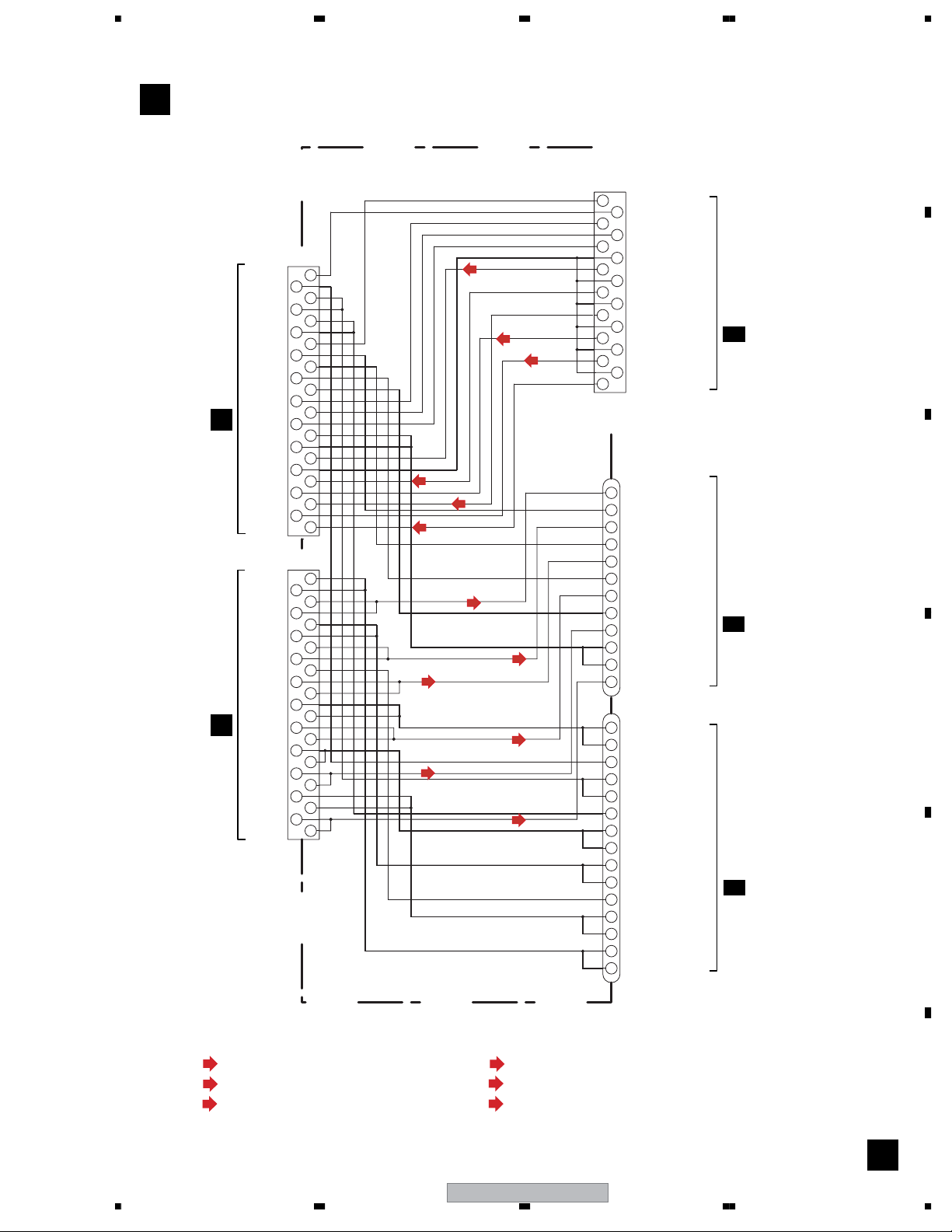
TRADE ASSY
H
(XWZ4149)
5678
A
CKS3382
CN3031
17
XPROT
RYRC
3
RYFS
42
MUTEC
5
MUTE
RYRC
GNDF
UN+8V
UN+8V
GNDREG
GNDREG
XPROT
VD+5
VA-12
VP+12
VFL+5
CN3002
RYFS
MUTEC
I
MUTE
VPR+8
VPR+8
FLIN
GNDA
FRIN
SWIN
CIN
SLIN
SRIN
VHVH-
SROUT
SROUT
GNDP
GNDP
SLOUT
SLOUT
GNDS
COUT
COUT
VH+
CN3001
VH+
I
SWOUT
SWOUT
VL+
VL+
FROUT
FROUT
FLOUT
FLOUT
CN3021
XKP3055
2
4
6
8
10
11
12
13
14
15
16
17
18
19
20
21
22
23
CN3022
XKP3055
1
2
3
4
5
6
7
8
9
10
11
12
13
14
15
16
17
18
19
20
VL-
21
VL-
22
23
1
3
5
7
9
(FR)
(SR)
(C)
(FR)
(FL)
(SW)
(SL)
(C)
(SR)
(SL)
(SW)
(FL)
9
1311
1715
6
810
12
14
16
J3032
12
11
10
9
8
7
6
5
4
3
2
1
1
2
3
4
5
6
7
8
9
10
11
12
13
14
15
J3033
GNDA
FLIN
GNDA
FRIN
GNDA
CIN
GNDA
SWIN
GNDA
SLIN
GNDA
SRIN
51048-1200
SROUT
VD+5
SLOUT
VA-12
COUT
VP+12
SWOUT
VFL+5
FROUT
VPR+8
VPR+8
FLOUT
D20PYY1215E
VH+
VH+
GNDF
UN+8V
UN+8V
GNDREG
VL+
VL+
GNDP
GNDP
GNDS
VL-
VL-
VH-
VH-
51048-1500
D20PYY1515E
CN3003
2/3C
CN3302
3/3C
CN13
3/3C
B
C
D
E
(FL)
: AUDIO SIGNAL ROUTE(Lch)
(FR)
: AUDIO SIGNAL ROUTE(Rch)
(SW)
: AUDIO SIGNAL ROUTE(SUBWOOFER)
(C)
: AUDIO SIGNAL ROUTE(CENTER)
(SL)
: AUDIO SIGNAL ROUTE(SURRUND Lch)
(SR)
: AUDIO SIGNAL ROUTE(SURRUND Rch)
XV-EV9
56
F
H
37
7
8
Page 38
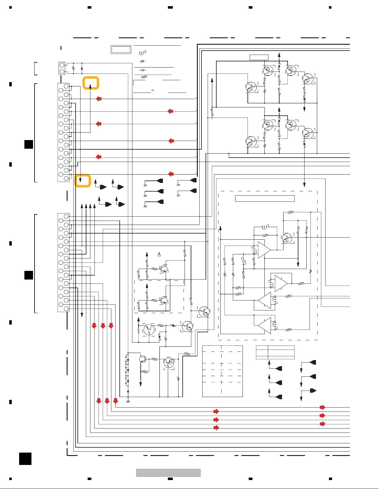
1234
3.11 AMP ASSY
A
NOTES
CN3651
KM200SA2
1
FAN+ ALL INDUCTORS ARE IN µH
2
FAN-
CN8004
FAN
1
VH-
2
VH-
GNDP
GNDP
SLOUT
SLOUT
GNDS
COUT
COUT
VH+
VH+
VL+
VL+
FROUT
FROUT
VL-
VLFLOUT
FLOUT
CN3001
CN3002
XKP3071
RYRC
GNDF
UN+8V
UN+8V
VD+5
VA-12
VP+12
VFL+5
RYFS
MUTE
VPR+8
VPR+8
FLIN
GNDA
FRIN
SWIN
CIN
SLIN
SRIN
3
4
5
6
7
8
9
10
11
12
13
14
15
16
17
18
19
20
21
22
23
XKP3071
1
2
3
4
5
6
7
8
9
10
11
12
13
14
15
16
17
18
19
20
21
22
23
SROUT
SROUT
B
CN3022
SWOUT
SWOUT
H
C
GNDREG
GNDREG
XPROTECT
MUTEC(STBY)
CN3021
H
D
E
F
C3653
47/25
GNDA
GNDP
GNDS
VH-
VD+5
VA-12
1SS133
D3655
VH+
VFL+5
VP+8
VP+12
(SW)
MUTE
MUTEC(STBY)
(SR)
(C)
(FR)
VFL+5VD+5
VD+5
VP+8 VP+12
VP+8 VP+12
(SR)
(FL)
(C)
(FR)
(SL)
ALL CAPACITORS ARE IN µF
UNLESS OTHERWISE SPECIFIED
ALL RESISTORS ARE IN Ω
*1
R3317,3318,3319,3320,3518
R3520,3417,3419,3418,3420
R3517,3519
GNDA
VFL+5
GNDP
GNDS
R111
R121
VPF+12
R3657
C
STBY
W124
E
D3654
2SD2144S(UV)
STBY STBY
W123 W108
D3652 D3653
D3651
1SS133
GNDF
CH : CCSRCH
CJ : CCSRCJ
(OTHER : CKSRYB)
CEAT
LAU***J
RS1/16S***J
VD+5
TH111
NCP18WF104J03RB
R113
R112
1k
1k
VD+5
STBY
R123
TH121
STBY
R122
Q3652
DTA124TK
E
33
Q3654
R3655
B
R3656
22k
VF-12
:ACN7122 or ACN7123
(SW)
GNDF
GNDA
GNDP
GNDREG
GNDS
C
Q111
B
STBY
C
Q121
B
STBY
R3658
2.2k
D3657
(UN5112)
2SC4081(QR)
E
C
E
D3658
UDZS3R9B
MA111
C3652
47/50
Q3653
DTA124EUA
C
E
B
C3651
220
STBY
STBY
B
8.2k
(SL)
(FL)
100/25
B
Q3651
RN1901
(1/2)
GNDF
GNDREG
XPROTECT
0
R114
R3654
R3651
3.3k
C
E
UN+8V
AOUT
1.8k
B2
Q3651
RN1901
(2/2)
*
VL+
VD+5
R108
XPROTECT
C2
E2
Wiring
No.
Unit
No.
C3317
C3318
R3313
R3314
R3372
R3373
C3301/C3302
C3502/C3401
C3168/C3178
C3402/C3501
C3167/C98
(SR)
(FL)
(SW)
27k
(6CH/DX)
PROTECT
Q101
UMB1N
(RN2903)
(1/2)
C
B
E
Q102
UMH1N
(RN1903)
(1/2)
Q103
UMB1N
(RN2903)
(1/2)
C
B
E
Q104
UMH1N
(RN1903)
(1/2)
Godzilla Amp (SIGNAL CLIP DETECTOR)
STBY
VP+12
IC3305
C3677
STBY
5
C3676
R3676
100k
68k
0.01
R3678
STBY
1
HA17558AF (1/2)
7
HA17558AF (1/2)
IC3401
VH+
VL+
UN+8
680
R3674
R3673
C3673
C3674
47/25
R3675
R3677
100k
AUDIO NEXT
XWK3262
STBY
STBY
3.9k
3.9k
0
0
CEAL****
E-CAPS
(MINIATURE)
680
47/25
MUTEC(STBY)
MUTE
E
C
1k
R101
C101
VP+12
E
C
1k
R104
1/50
C102
VL-
C3678
0.01
R3679
68k
-
86
+
HA17558AF (2/2)
4
C3679
4
+
IC3304
-
-
IC3304
+
8
*B
AudioNexT Series
Unit
No.
VH+
D101
B
R102
1/50
R103
D102
B
R105
R106
C
E
7
-
2
IC3305
+
STBY
3
3
2
6
5
(6CH-DX)
STK433-270
VH+
VL+
UN+8
Q101
UMB1N
(RN2903)
(2/2)
E2
MA111
Q102
C2
UMH1N
10k
(RN1903)
(2/2)
10k
Q103
UMB1N
(RN2903)
(2/2)
E2
MA111
C2
Q104
10k
UMH1N
(RN1903)
(2/2)
10k
VA-12
R3681
39k
Q3660
DTA124EUA
VA-12
1
HA17558AF (2/2)
R3671
10k
R3672
STBY STBY
C3672 C3671
10k
VH-
VL-
VA-12
B2
B2
R3683
B
R3680
470
CH2IN
CH2NF
E2
C2
E2
R109
D106
1M
UN+8V
C2
D105
R3682
VL+
B2
820
UDZS7R5B
VH-
B2
UDZS7R5B
680k
C3680
VH-
VL-
VA-12
1/50
(SL)
(C)
(FR)
38
I
XV-EV9
1234
Page 39

(SL)
D3389
D3390
(C)
MTZJ10B
R3385
R3386
MTZJ10B
30PDA20-FC6
D3391
D
S
3
2
G
1
Q3383
100
R3387
Q3381
C
E
15k
2SC4081(QR)
Q3382
E
15k
C
2SA1576A(QR)
R3388
100
2
G
3
1
Q3384
S
D
D3392
30PDA20-FC6
C3167
2.2/50
C3168
2.2/50
C3178
2.2/50
C3317
R3372
R3373
*
C3318
C3179
R3374
5678
AMP ASSY
I
D3393
2SJ304
D3387
1SS133
B
R3383
R3384
B
D3388
D3394
2SK2232
R3413
R3414
R3513
*
*
*
10/50
STBY
R3389
MTZJ18B
100k
D3385
D3386
100k
R3390
MTZJ18B
100k
100k
100k
*
R3313
*
R3314
47k
R3514
VH+
VL/VH
100k
R3381
10k
MTZJ36B
R3382
10k
MTZJ36B
1SS133
100k
VH-
VL-
R3500
STBY
R3371
0
R3667
STBY
R3668
STBY
(FR)
R3669
STBY
W240
SLOUT
SROUT
FROUT
FLOUT
SWOUT
COUT
R61
VD+5
STBY
D3381
DAN217
D3382
DAN217
D3481
DAN217
D3482
DAN217
D3581
DAN217
D3582
DAN217
R3391
0
R3392
0
R3491
0
R3492
0
R3591
0
R3592
0
VL+
R3401
1k
R3403
B
2.2k
Q3401 (1/2)
XP4506
Q3401 (2/2)
XP4506
R3404
B
2.2k
(SR)
E
Q3504
STBY
B
C
(FL)
C3661 C3301
STBY
R3661 R3662
D
00
G
Q3655
S
STBY
Q3656
S
STBY
G
D
R3663 R3664
00
C3662
STBY
C3663
STBY
R3665 R3666
D
00
G
Q3657
S
STBY
R3402
1k
R3501
1k
R3503
B
2.2k
Q3501
2SD2114K(VW)
R3301
470 2.2/50
R3303
B
2.2k
Q3301 (1/2)
XP4506
Q3301 (2/2)
XP4506
R3304
B
2.2k
R3302
470
(SW)
R3502
470
R3504
2.2k
Q3502
2SD2114K(VW)
D3604
STBY
D3603
STBY
D3601
STBY
C66
0.047
R64
STBY
R62
Q63
STBY
C61
C3401
2.2/50
E
C
C
E
C3402
2.2/50
C3501
2.2/50
E
C
E
C
C
E
C3302
2.2/50
W242
B
STBY
GNDA
C3502
2.2/50
D3602
STBY
STBY
E
D3605
STBY
W241
W243
TA7812S
Q61
STBY
C
C
Q62
STBY
B
R63
C
E
R65
IC61
B
STBY
R67
STBY
R85
STBY
3W
OUTIN
E
R66
R3305
R3306
R3506
R3405
R3406
R3427
R3505
UN+8V
VP+12 VPF+12
STBY
C63
CH
C62
STBY
R68
STBY
STBY
D42
MA111
IC3301
STK433-270
R3307
220
56k
C3303
56k
C3304
R3308
220
R3327
D3327
1SR139
(1/4W)47
R3508
220
56k
C3504
R3407
220
56k
C3403
56k
C3404
R3408
220
D3427
(1/4W)47
1SR139
R3507
220
56k
C3503
350mA
22/50
D63
MTZJ18B
1000p
C3305 C3309
47p CH
1000p
D3321 D3323
1SR139
1000p
C3323
1000p
C3405 C3409
47p
CH
1000p
D3421 D3423
1SR1391SR139
1000p
C3423
UN+8V
C71
-PRE
12
R3309
C3307
220/50
*B
IC3401
-PRE
R3409
220/50
(XWK3262)
(FL)
: AUDIO SIGNAL ROUTE(Lch)
(FR)
: AUDIO SIGNAL ROUTE(Rch)
(SW)
: AUDIO SIGNAL ROUTE(SUBWOOFER)
IC81
C72
OUTIN
10/50
C82
D72
VA-12
350mA
D82
47/25
MTZJ15B
250mA
VF-12
C81
0.047
0.047
OUTIN
IC71
TA79012S
TA7805S
SR,SL,C POWER AMP
-VCC
+VCC
CH1 OUT
3
R3317
2W0.22
R3311
56k
CJ8p
1.5k
AL
10/16
R3321
STBY
D3325 D3326 D3324 D3322
1SR139 1SR1391SR139 1SR139
1SR139
GNDP
+PRE
CH2 OUT
CH2 OUT
CH1 OUT
5468710119
0.222W
R3318
R3323
AL
C3321
0.22/100
SUB
R3351
1
AL
FR,FL,SW POWER AMP
CH2 OUT
CH1 OUT
CH1 OUT
-VCC
21
R3411
56k
C3407
R3421
STBY
GNDA
GNDP
GNDS
1.5k
+VCC
3
8p
10/16
R3417
CJ
AL
0.22
D3425 D3426
1SR139
SUB
+PRE
CH2 OUT
5476810119
R3418
R3451
2W0.22
1
R3423
1SR139
C3421
AL
AL
0.22/100
GNDP GNDA
UN+8V
VFL+5VD+5
10k
R46
E
MTZJ7.5B
B
C
R45
R47
470
4.7k
C91
1%4.7k
R48
CH1 IN
CH1 NF
GND
CH2 NF
ST-BY
1412 13 15 16 1817 19
5.6k
R3396
1
R3312
56k
C3310
C3306
47pCJ CH CH47p
8p
R3310
1
R3324
C3308
R3322
STBY
C3322
0.22/100
CH1 NF
CH1 IN
GND
CH2 NF
ST-BY
1
5.6k
R3496
R3412
56k
C3410 C3406
8p2WCJ 47p CH CH47p
1
R3424
R3422
STBY
D3424 D3422
1SR139
1SR139
C3422
0.22/100
D91
UDZ18B
Q43
2SA1576A(QR)
1%
R93
B
220
STBY
C92
0.1
CH3 OUT
CH3 NF
CH3 IN
CH2 IN
R3518
0.22
1.5k
10/16
AL
C3324
220/50
CH2 IN
CH3 OUT
CH3 NF
CH3 IN
151412 13 16 17 18 19
R3517
1.5k
*XV-EV1000,
C3408 R3410
10/16
AL
C3424
220/50
R91
100k
Q92
2SC4081(QR)
C
E
1%
R94
2.7k
CH3 OUT
2W
E
C3506
R3326
C3326
CH3 OUT
2W
0.22
E
C3505
XV-EV700
ONLY
Series
R3426
C3426
Q91
2SJ304
S
3
G
1
R92
1%1%CH
R96
R97
10k
R95
2.7k
GNDREG
33k
R3395
B
Q3385
2SC4081(QR)
C
R3512
56k
C3510
1.5k
R3510
10/16
C3508
D3328
1SR139
STBY
STBY
GNDS
GNDP
33k
R3494
R3495
D3401
B
2SC4081(QR)
C
Q3485
R3511
56k
C3509
8p CJ
R3509
C3507
D3428
1SR139
STBY
STBY
D
2
100
C97
10k
SENSE+8
1%
1k
R3394
D3301
MA111
CJ8p
AL
MA111 1k
AL
47/6.3 1.5k
GNDS
220p
C3311
(SR)
(SL)
R3328
(1/4W)
R3493
C3312
(SW)
(FR)
(FL)
R3428
VP+8
R3687
R3393
47/25
(C)
47
2.2k
47/25
(1/4W)47
C98
47/25
27k
D98
MTZJ11B
2.2k
A
B
C
D
E
GNDA
GNDP
GNDS
MUTE
(C)
: AUDIO SIGNAL ROUTE(CENTER)
(SL)
: AUDIO SIGNAL ROUTE(SURRUND Lch)
(SR)
: AUDIO SIGNAL ROUTE(SURRUND Rch)
XV-EV9
56
F
I
39
7
8
Page 40

1234
3.12 WAVEFORMS
Note : The encircled numbers denote measuring point in the schematic diagram.
DVDM ASSY
B
A
Measurement condition ;
No. 1 to 10 : reference A1 (DVD), T2-chp 19, Color-bar
No. 11 to 14 : reference A1 (DVD), T1
IC201-pin50 [FG]
1
V: 1V/div. H: 2msec/div.
B
IC201-pin 39 [TROPENPWM]
2
V: 1V/div. H: 5µsec/div.
[Tray stops]
[Tray is opening] [Tray is closing]
GND
GND
GND
GND
C
IC201-pin37 [DMSO]
3
V: 1V/div. H: 10µsec/div. V: 1V/div. H: 10µsec/div. V: 1V/div. H: 2sec/div.
D
CN102-pin 11, 10, 9 (IC101-pin 30, 33, 36)
4
[SPINDLE (WVU)]
V: 2V/div. H: 2msec/div.
[TRAY OPEN] [DVD PLAY] [DMSO]
GND
GND
GND
PLAY
Pless OPEN key Pless PLAY key
Braking a turn of disc
Tray :
opening
GND
E
IC401-pin23 [CompositeVideo Out]
89
V: 1V/div. H: 10µsec/div.
GND
IC401-pin21 [S VIDEO OUT - Y]
V: 1V/div. H: 10µsec/div.
IC401-pin26 [S VIDEO OUT - C]
0
V: 1V/div. H: 10µsec/div.
F
40
XV-EV9
1234
9
9
10
GND
10
GND
Page 41

5678
Note : The encircled numbers denote measuring point in the schematic diagram.
MAIN ASSY
C
A
1 IC5501 - Pin 28 [FLCLK]
2 IC5501 - Pin 27 [FLDATA]
5 IC5501 - Pin 84 [2CHVOLCLK]
6 IC5501 - Pin 85 [2CHVOLDATA]
7 IC5501 - Pin 25 [SCLK]
8 IC5501 - Pin 23 [SDATA]
3 IC5501 - Pin 96 [(6CH)VOLCLK]
[ANY FUNCTION]
[VOL UP/DOWN]
4 IC5501 - Pin 97 [(6CH)VOLDATA/CE]
9 IC5501 - Pin 24 [MDATA]
[DVD] [DVD]
[VOL UP/DOWN]
B
C
0 IC5501 - Pin 61 [TXCLK]
- IC5501 - Pin 62 [TXODATA]
~ CN3301 - Pin 3 [D+]
! CN3301 - Pin 2 [D-]
[USB
(USB PLAYER CONNECTED)]
D
= IC5501 - Pin 66 [TXIDATA]
[TUNER] [TUNER]
E
F
56
XV-EV9
41
7
8
Page 42

1234
4. PCB CONNECTION DIAGRAM
NOTE FOR PCB DIAGRAMS :
A
1. Part numbers in PCB diagrams match those in the schematic
diagrams.
2. A comparison between the main parts of PCB and schematic
diagrams is shown below.
Symbol In PCB
Diagrams
BCE
BCE
B
D
Symbol In Schematic
Diagrams
BCEBCE
BCE
DGGSS
BCE
DGS
Part Name
Transistor
Transistor
with resistor
Field effect
transistor
Resistor array
3-terminal
regulator
3. The parts mounted on this PCB include all necessary parts for
several destinations.
For further information for respective destinations, be sure to
check with the schematic diagram.
4. View point of PCB diagrams.
Connector
Capacitor
SIDE A
P.C.Board
Chip Part
SIDE B
C
D
4.1 LOAB ASSY
SIDE A SIDE B
LOAB ASSY
A
VNP1836-C
S101
5
51
(VNP1836-C)
CN602
12
LOAB
VWG2279VWG2346-
1
CN601
VWG
5
E
LOAB ASSY
A
PNE-1B1
GND
(VNP1836-C)
(V+5D)
V+3D
15
SW2
C102
C101
51
LOAD+
LOAD-
CN601
CN602
CN601CN602 CN601 CN602
CN104
B
LOADING MOTOR
F
M
ASSY
A A
42
1234
XV-EV9
Page 43

5678
4.2 TRADE ASSY
SIDE A
250
240
230
220
210
200
190
180
170
160
150
Y
140
H
TRADE ASSY
1
J3033
CN13
12.VL-
13.VL-
14.VH-
15.VH-
J
3032
15
1
C
J3032
CN3302
C
12
1. FLOUT
2. VPR+8
3. VPR+8
4. FROUT
5. VFL+5
6. SWOUT
7. VP+12
8. COUT
9. VA-12
10. SLOUT
11. VD+5
12. SROUT
2CH
6CH
(XNP3108-C)
10.COUT
11.COUT
12.VH+
9.GNDS
1.VH+
2.VH+
J
3033
3.GNDF
4.UN+8V
5.UN+8V
6.GNDREG
7.VL+
8.VL+
9.GNDP
10.GNDP
11.GNDS
W362
W357
W351
W356
TRADE ASSY
VP+12
W358
W354
W359
W360
VA-12
23.FLOUT
VL+
W364
21.VL-
22.FLOUT
W363
GNDREG
15.SWOUT
14.SWOUT
13.VH+
R
VPR+8
12.VH+
XWZ4149
XWZ4151
11.CIN
9.FRIN
5.MUTE
9
10.GNDA
7.FLIN
6.GNDA
4.MUTEC
3.RYFS
2.RYRC
1.XPROT
8.GNDA
CN3034
12.GNDA
CN3031
13.SWIN
14.GNDA
15.SLIN
7.SLOUT
8.SLOUT
20.VL-
19.FROUT
W361
10.COUT
11.COUT
W352
17.SRIN
16.GNDA
6.GNDP
18.FROUT
W365
GNDF
9.GNDS
8.SLOUT
W353
4.SROUT
5.GNDP
16.VL+
17.VL+
W366
7.SLOUT
6.GNDP
5.GNDP
19.FROUT
18.FROUT
23.FLOUT
22.FLOUT
17 1
1.VH-
2.VH-
3.SROUT
13.VH+
14.SWOUT
15.SWOUT
1
VH+
W367
23
4.SROUT
3.SROUT
2.VH-
1.VH-
16.VL+
17.VL+
1
21.VL-
20.VL-
23
W337
GNDA
CONTACT
SIDE
CN3022 CN3021
OPEN
OPEN
CN3022
CN3021
CN3031
I
CN3001
I
CN3002
C
CN3003
1.VH-
2.VH-
3.SROUT
4.SROUT
5.GNDP
6.GNDP
7.SLOUT
8.SLOUT
9.GNDS
CN3031 CN3021 CN3022
1
10.COUT
11.COUT
12.VH+
13.VH+
14.SWOUT
VH+
15.SWOUT
16.VL+
17.VL+
18.FROUT
19.FROUT
20.VL-
21.VL-
22.FLOUT
23.FLOUT
23
5.GNDP
4.SROUT
3.SROUT
1.VH-
2.VH-
123
17.VL+
18.FROUT
16.VL+
19.FROUT
GNDA
XWZ4149
XWZ4151
6.GNDP
7.SLOUT
20.VL-
22.FLOUT
GNDF
8.SLOUT
9.GNDS
21.VL-
23.FLOUT
GNDREG
11.COUT
10.COUT
VPR+8
16.GNDA
17.SRIN
15.SLIN
12.VH+
14.GNDA
VL+
14.SWOUT
13.VH+
VA-12
12.GNDA
13.SWIN
15.SWOUT
R
10.GNDA
11.CIN
9.FRIN
7.FLIN
8.GNDA
11
91
10
6.GNDREG
1.VH+
1
2.VH+
3.GNDF
4.UN+8V
5.UN+8V
7.VL+
8.VL+
6.GNDA
10.GNDP
VP+12
4.MUTEC
5.MUTE
9.GNDP
3.RYFS
10
11.GNDS
12.VL-
13.VL-
14.VH-
15
15.VH-
TRADE ASSY
1
12
1. FLOUT
2. VPR+8
1.XPROT
3. VPR+8
2.RYRC
4. FROUT
5. VFL+5
6. SWOUT
7. VP+12
1 17
8. COUT
9. VA-12
10. SLOUT
11. VD+5
12. SROUT
(XNP3108-C)
J3033
J3032
SIDE B
250
240
230
220
210
200
190
180
170
160
150
140
A
B
C
Y
240 250 260 270 280 290 300
X
240250260270280290300
X
D
E
F
H H
56
XV-EV9
7
8
43
Page 44

1234
4
4.3 DVDM ASSY
SIDE A
A
B
DVDM ASSY
150
140
130
120
110
CN8002
D
100
90
80
70
CN903
Q565
C562
44
GNDM
R741
CN903
C143
C141
C145
C146
23
C132
Q801
C734
UP SIDE
1
R579
R578
16
R536
R535
1
C561
R533
R534
C133
C142
C144
C161
D801
D851
R750
L751
IC731
C735
C538
R555
R556
R552
Q534
IC531
C534
C530
R530
R532
L308
LD_DVD
L309
LD_CD
3
4
35
R733
D733
9
R531
C801
1
R732
C539
C541
C542
R550
R551
Q533
8
R325
Q307
R322
D852
R821
5
21
C736
R326
Q308
R321
R737
R743
R742
Q731
R801
C568
C569
R573
R571 R572
R373
4
Q305
3
R315
Q304
R574
C374
R566
IC561
R565
R318
R135
R134
R133
R132
R131
IC761
R751
C751
R731
C731
C573
C574
R567
R564
R313
R136
C101
R568
16 9
1
1
R563
B
R
R585
C571
C572
1
5
1
C371
CN101
24
CN102
C140
R703
C373
Q701
C701
R586
R314
R905
R903
GNDD
R901
Q702
5
1
R152
R154
R915
R914
R913
R912
R911
R910
R908
R907
8V/6.5V
C702
D751
CN103
UP SIDE
FR4 P
CN103
STEPPING MOTOR
BOTTOM SIDE
C
80 90 100 110 120 130
CN101
PICKUP ASSY
BOTTOM SIDE
1
D
CN102
12
1
SPINDLE MOTOR
CN901
UP SIDE
E
20 30 40 50 60 70
CN901
CN5502
C
12V
27
8V/3.3V
R702
R701
B
F
10
X
Q561
R575
R576
Q562
R569
C152
C103
R762
Q564
Q563
C564
C151
C104
R151
R153
R761
5
7
IC751
GNDD
R537
R582
8
C153
1
22
R763
C732
R538
R581
R764
C762
L731
R539
R557
C563
6.5V
C763
1
Q851
R851
R852
R853
R736
R561
IC101
C131
C761
C752
4
C753
5V
7
C102
C754
C733
R543
R541
R542
R544
C533
3.3V
3.3V
C203
D861
D862
D821
R822
R823
R824
R712
C543
C544
C531
C206
Q821
R713
L732
R545
R546
R548
Q535
C532
R310
C320
L761
C712
R714
R739
Q531
R528
R527
3.3V
C738
4
R549
IC501
Q532
R769
R770
5
C711
C739
Q506
R506
C309
C310
C209
C211
R734
R507
Q503
16
1
R505
R504
C208
C210
C212
R767
8
R509
R508
R503
R595
R594
C3
R768
1
IC711
R711
D731
R740
44
B
XV-EV9
1234
Page 45

80
70
5678
SIDE A
A
Y
60
50
40
CN3001
C
30
20
10
0
R545
R546
R548
Q535
1
R310
C320
L761
C712
Q531
R527
C532
R714
3.3V
R739
R549
R528
R769
R770
4
C738
Q506
IC501
R506
Q532
5
C711
C739
R507
1
R505
C309
C310
C209
C208
C210
C211
C212
R734
Q503
16
R504
R595
R594
R767
1
IC711
8
R509
R508
R503
C345
R768
R711
R740
D731
R520
9
8
C504
C347
R204
R205
C221
R206
R214
C713
R735
R738
C737
Q504
R525
R526
C343
R238
R239
R201
R202
C740
C503
R284
C508
R592
R256
C346
C344
5040
64
R232
C509
C511
C512
R501
C501
C273
1
1.8V
C714
C272
256
65
R217
R514
C269
C271
C220
R513
R593
C268
R511
R512
C514
C258
C259
R200
C201
C513
R522
IC591
3
4
X201
C251
R252
R224
R510
R521
R518
C502
1
R591
5
4
R502
R519
Q505
R240
9070
R221
1
IC204
R
L
C252
R251
R253
100
27
Q501
R515
R516
Q502
C454
8
5
GNDA
C240
R222
C476
C451
Q401
R242
C241
C248
R241
R243
C245
R279
120110
R259
C290
R218 R219
GNDD
CN902
C475
5V
R230
R244
R260
C474
C426
R401
128
R262
R246
R245
193
R263
1
GNDD
R405
170150
129
C425
C424
R413
R411
R412
R414
R415
R416
192
IC201
R225
UP SIDE
V
C423
C422
R404
C237
R264
R265
R266
R267
R271
R227
R226
R229
R228
4
C421
C250
CN204
C404
CN902
1
R921
R922
R924
R481
4
1
C281
R923
Q481
CN104
121
R433
R431
R432
R434
R435
R436
CN905
121
CN904
A
1/2
2/2
(ANP7577-A)
CN104
B
A
CN601
C
D
E
F
56
XV-EV9
B
45
7
8
Page 46

A
N
B
C
D
E
SIDE B
1234
B
DVDM ASSY
Y
0
10
20
30
40
50
60
70
80
CN902
R1003
R1002
R517
CN104
R1001
C401
R403
C402
28
R402
C406
1
C411
C403
R421
C412
C284
C285
54
R422
R209
C232
C230
28
R423
C413
C231
C229
IC202
R281
R424
C405
C246
C243
C244
R425
C414
C270
R426
C415
R269
C236
C235
C282
15
14
C416
IC205
C233
27
C452C453
16
1
IC401
C283
R203
1
R475
R474
C464
C465
13
R257
54
C223
R250
C247
R247
R248
C234
C225
C288
C296
C289
C287
R261
R223
C286
R476
9
8
C455
C466
R234
IC451
C242
C224
R231
25
R285
R220
C227
C222
C239
C228
48
R235
R596
R249
R237
C262
R254
C254
R598
C266
C260
C261
C238
R233
R597
C264
R236
C226
R590
C591
C256
C255
C207
C200
IC203
C592
C219
C217
CN951
1
C204
C205
C267
C265
R255
R212
R207
C213
C218
R213
C202
C216
1
C214
R523
C500
C215
24
R282
R524
R919
R920
13
R500
R210
R211
R208
C
2
F
B
46
1234
XV-EV9
Page 47

5678
SIDE B
A
R920
13
R500
80
R547
90
R554
R553
100
CN903
R587
R588
110
R577
R560
C560
CBA
120
R601
R584
R583
R918
FCICT
R603
R371
R602
R604
R375
130
R374
R372
C372
R303
R301
R302
140
150
B
CN103 CN101
C
R210
R211
R208
CN952
12
Q732
13
64
R882
D732
R883
R881
D881
123456789
0
1
123
0
0
Q881
R752
AWM8
000
111
DVDM ASSY
1
0
C121
222
R765
Production Code
333
444
555
LF
666
777
888
R917
R909
R916
R906
R904
L901
999
R902
(ANP7577-A)
CN102 CN901
20 30 40 50 60 70 80 90 100 110 120 130
10
D
E
X
F
56
XV-EV9
B
47
7
8
Page 48

1234
6
W
4.4 MAIN ASSY
SIDE A
A
C
MAIN ASSY
TUNER MODULE
J
CN8001
D
W436
CONTACT
GND
10 RDS
NC(VSM)
TXR
+9V
TXL
5 GND
D0
CLK
DI
1 CE
W350
C3021
C3019
C2401
C2410
W293
W292
C2409
W261
CN2507
13
C2305
W180
W178
W179
W177
C2814
C2813
L2812
TA7805S
W117
SIDE
C5904
W119
W118
W101
10
CN5505
W438
W437
W512
SIDE
CN5505
W263
W262
C2815
C2816
C2306
L2811
1 TIMERLED
W102
C2402
W221
D2307
VR2802
W411
W377
C3024
C3023
C2321
C5903
1
REMOCON
GNDU
W511
W510
C2325
C2808
Q2302
14
BIG
VP+12
11
1
W351
D2306
5 VE+5
W412
C3036
C3014
W260
C2803
Q2801
CN5504
W461
JOG
KEY2
D2304
W413
C3035
C2802
W121
GNDLED
KEY1
C2322
C2801
L2801
D2302
W414
W181
CN2301
W104
W378
R2805
1
Q2301
VR2801
W415
C3041
IC3001
C3013
W222
W182
CONTACT
10 FLAC1
W327
C2326
Q2802
CN2302
19
SIDE
FLAC2
C5704
C3042
C2807
R2803
C2804
Q2806
R5807
W151
W147
W123
MOVIELED
MUSICLED
C2323
W149
1 GNDM
1
15 FLDATA
GNDFL
L2802
C2810
SOL
W124
W379
C3060
NC
FLCLK
R2815
R5802
W125
FLCS
W224
W223
PULSE
VFDP
L2101
C2105
C3055
W225
W183
5 HALF
MODE
W126
VFL+5
W416
W417
Q2805
W264
W188
W148
GNDMTC
VD+5
C5701
RECF
C3045
C3054
C2324
10 MOTOR
W460
20 30 40 50 60 70 80 90 100 110 120 130 140
C2103
C3056
W525
C2805
W270
W226
W227
W185
W184
W186
RECR
CONTACT
W105
D2101
W265
W228
W187
11
SIDE
W130
D2102
W302
W269
W272
W268
W267
W266
W150
CN5503
7
C3046
W353
W380
W355
CN5501
C3108
W352
W418
W383
W127
W385
W354
C3059
W271
C3057
C5609
W152
C3080
W299
W298
W153
W128
1
W381
W382
W330
W329
W301
D5621
W229
W230
W129
W154
W106
CONTACT
SIDE
JA3001
W517
C3061
W328
W231
C5606
W155
1 NC
GNDU
VE+5
XRESET
5 FLASH CLK
FLASH D0
FLASH E/D
W300
W131
C3107
W189
W516
C3064
W232
W233
W156
C3069
C3068
W190
W132
C5610
W384
W390
W337
W331
W235
W191
W356
W157
NP
W332
JA3002
W386
IC3032
IC5502
CN3301
W234
NP
W158
W387
W303
L5601
W192
IC3033
W159
W333
13
W108
FR
W273
C5602
HPL
C3004
W389
C3066
W518
W334
W160
GNDHP
230
220
210
200
B
190
180
170
160
150
C
140
130
120
110
100
D
90
80
70
60
TAPE DECK
CN2302
MECHA CN8011
CN2301
50
E
40
30
20
10
MECHA CN8012
TAPE DECK
IC5902
CN5503
PRINTED
CN5504
CN5301
Y
0
F
E
0
C3065
W335
W304
HPR
W555
C3003
W419
FL
W388
W357
W358
W338
W339
W310
W309
W308
W307
W305
W306
W161
W559
10HPDET
ECHOVOL
GND
W336
W311
VA+12V
10
CN3004
W440
W421
W393
W394
W395
W360
W313
W312
X5601
W134
5 MICSW
GNDA
MIC
LINE(R)
SIDE
OPEN
CN3004
W274
W135
GNDUSB
D+
W420
W424
W423
1
W275
W392
W391
W396
23
20 GNDA
15 FRIN
MUSIC
FRTSURR
EDATA
ECLK
5 EXPWRM
VA+12
FR
GNDA
1 FL
W276
IC5501
W539
D-
LINE(L)
W422
SRIN
GNDD
SLIN
SWIN
GNDA
CIN
GNDA
GNDA
FLIN
VA-12
W340
ABYPASS
10 MOVIE
W314
W277
W193
W162
W166
1 V+5USB
1
1
W359
W164
W317
W316
W315
W278
W552
R3462
C19
W560
W441
L3462
W399
W398
C12
W279
W280
W281
W236
W237
W238
W194
W167
W1
W173
W168
5
W551
W549
W550
W548
X
C
48
1234
XV-EV9
Page 49
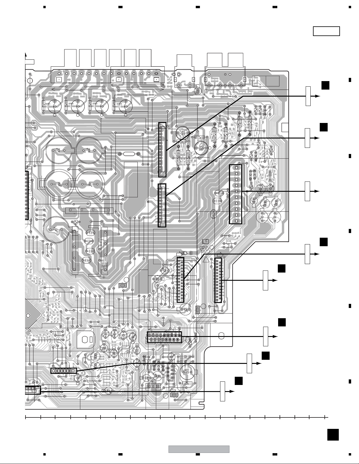
0
001
004
5678
SIDE A
A
LINE(L)
W42
W441
W422
W399
W281
W167
W168
W238
W169
W173
W547
W425
R8883
L3461
W363
W362
W342
W341
C25
W532
W558
W195
W171
W196
W172
W170
J
12
15
4 VE+5
1 SYSPOW
3 SUBAC
2 GNDU
5 XPROT
R13
D17
W197
W538
C5608
W424
R3462
W423
1
W275
W392
W391
W396
23
20 GNDA
15 FRIN
MUSIC
FRTSURR
EDATA
ECLK
5 EXPWRM
VA+12
FR
GNDA
1 FL
W276
IC5501
W539
D-
SRIN
GNDD
SLIN
SWIN
GNDA
CIN
GNDA
GNDA
FLIN
VA-12
W340
ABYPASS
10 MOVIE
W314
W277
W193
W166
1 V+5USB
W359
W164
W162
1
1
W317
W316
W315
W278
W552
L3462
W398
C19
C12
W279
W280
W236
W237
W194
W551
W549
W550
W548
W560
C13
C14
C24
W239
W537
R3461
L3661
W442
W426
W443
R3561
W444
L3561
PRODUCTION CODE
W366
C20
W364
W365
IC16
491007
C11
W521
W343
W522
MAIN
D11
ASSY
W201
GNDM
W536
W499
17 SRIN
D12
W243
GNDA
C3126
16 GNDA
C3113
C3128
W283
W244
VFL+5
15 SLIN
14 GNDA
W540
W320
W528
FL
13 SWIN
W535
IC3110
12 GNDA
B2
W527
VA-12
C3117
11 CIN
W534
W319
C15
W282
W240
W198
W200
W199
W174
XPROT
XHPMUTE
W557
C3119
C3124
C3127
NP
C3112
NP
W545
W546
W543
W544
W541
W542
LITTLEFUSE INC.
REPLACE IC LINKS AS
MARKED. M'FD BY
CAUTION
VFL+5
W286
W285
W245
W526
VA+12
FR
8 GNDA
10 GNDA
9 FRIN
C3110
W553
W554
C3115
VP+12
W287
W202
2 RYRC
C3122
C34
VFL+5
XPROT
W556
1 XPROT
7 FLIN
W113
W367
VA-12
W203
6 GNDA
D18
1 VH+
5 UN+8V
W520
W524
17
5 MUTE
Out
W427
VH+
GNDF
UN+8V
GNDREF
10 GNDP
15 VH-
W250
4 MUTEC
3 RYFS
D15
R14
W400
VL+
VL+
GNDP
GNDS
VLVLVH-
W346
C5526
CN3003
W144
W251
CN13
CN3302
REPLACE IC LINKS AS
MARKED. M'FD BY
CAUTION
W290
C5624
W252
D16
D800
SIDE
PRINTED
2SB1565
Q11
IN
1
1
W204
9
W533
C23
C3
JA3302
JA3301
W401
10 15
1 FLOUT
2 VPR+8
3 VPR+8
4 FROUT
5 VFL+5
6 SWOUT
7 VP+12
8 COUT
9 VA-12
10 SLOUT
11 VD+5
12 SROUT
10 12
CN5502
LITTLEFUSE INC.
W206
W205
SIDE
1
OPEN
R3362
CONTACT
W207
1 NC
W208
CN3005
W515
R3607
SIDE
W253
C5621
W209
127
2 NC
C22
CN5507
7
W145
JA3603
W403
CONTACT
SIDE
C21
GNDB
L3362
W368
W347
27 VDVD+12
491007
IC15
W531
6 CH
2 CH
1
D13
GNDD
W116
W428
R3608
W514
26 VPR+8
25 VPR+8
23,24
VPR+8M
21,22
GNDMDV
20 GNDDV
19 GNDDV
18 NC
17 GNDD
16 USBN
15 USBP
14 GNDD
13 DVDPOWER
W255
W254
12 XDVDRST
11 XREADY
10 SCLK
9 SDATA
8 MDATA
7 DVDACK
6 GNDD
5 GNDD
4 VDET
3 DVDMUTE
W529
W530
R16
D14
R12
W146
W115
R3361
R15
W513
W324
C3671
27 FR
25 FL
23 GNDD
21 GNDD
19 GNDD
17 GNDD
15 GNDD
13 GNDD
11 GNDD
A1
JA8801
W430
9 GNDD
7 GNDD
5 NC
3 NC
1 NC
W371
L3361
C16
W256
W211
C18
C17
R
27 1
W431
R3627
1 VFDP
5 BLAC2
BHAC2
SUBAC1
SUBAC1
10 FLAC2
CONTACT
CN3001
W212
CN3301
W405
W373
BHAC1
BLAC1
GND
R11
FLAC1
W291
SIDE
26 GNDA
24 GNDA
22 R
20 B
18 G
16 Cr/r
14 Cb/B
12 CY/G
10 SY
CN11
W523
W213
8 V
6 NC
4 NC
2 NC
W432
W406
R3628
W372
W407
W257
F
J5401
W374
W375
R3617
1
10
W409
R3634
D3632
R3635
W348
C3631
J12
R3631
R3618
C3632
C8851
R3632
W408
R3633
D3634
D3633
C8871
G
FCICT
D3631
W435
W410
R3668
W376
W349
C3633
CN3001
CN3003
CN3
C8861
C8881
B
CN902
H
CN3031
CN13
CN3302
CN11
CN5502
H
J3033
B
H
J3032
TRANSFORMER
(T1)
C
B
CN901
D
E
(XNP3107-D)
0130140 150 160 170 180 190 200 210 220 230 240 250 260 270 280 290 300 310 320
XV-EV9
56
7
8
F
C
49
Page 50

A
R5558
7
(
)
0
SIDE B
1234
C
MAIN ASSY
CN3
R5571
4 VE+5
R5570
R5596
R5603
5 XPROT
C3463
R5581
81
R3465
R3467
R3463
C3071
SRIN
GNDD
SLIN
20 GNDA
SWIN
GNDA
CIN
GNDA
15 FRIN
GNDA
FLIN
VA-12
ABYPASS
10 MOIVE
MUSIC
FRTSURR
EDATA
ECLK
5 EXPWRM
VA+1 2
FR
GNDA
1 FL
R5568
80
R5599
R5597
R5598
C3461
R3074
R5567
C3070
R5566
R5600
1 V+5USB
LINE(L)
R3075
R5563
R5565
R5569
100
R3084
R3080
R5501
R5611
D-
R3073
1
R5562
R3083
R3069
23
R5561
R5564
IC5501
D+
C3076
R5560
51
R5503
R30
R5559
1
R5504
5MICSW
GNDUSB
R
LINE
R5507
GNDA
C8862
R8866
R8865
L8821
R8822
C8822
R8821
R8823
Q3640
C3668
Q3612
R3638
Q3631
C3677
Q3635
D3613
R7006
R3651
R3614
R8880
Q3638
B
D3635
CN13CN3302
Q3639
Q3632
R7017
Q3633
C
R3639
CN11
D
CN3001
CN5502
E
R8854
R8853
R8855
R8856
D3612
D3611
R3611
R3615
R7005
R3616
R3669
D3636
110
Q3637
Q13
CN3003
C8852
L8851
C3676
R3613
Q3622
1 VFDP
GND
BHAC2
R18
26 GNDA
24 GNDA
22 R
R8873
R8876
Q3611
D3623
BHAC1
BLAC1
5 BLAC2
SUBAC1
SUBAC1
FLAC1
10 FLAC2
R17
20 B
18 G
16 Cr/R
14 Cb/B
12 CY/G
10 SY
8 V
6 NC
4 NC
2 NC
R3612
C3675
Q12
J12
C8872
R3624
R8872
R8875
R3626
L8871
R3621
R3625
R8864
D3622
D3621
Q3621
27 VDVD+12
26 VPR+8
25 VPR+8
27
27
27 FR
25 FL
23 GNDD
21 GNDD
19 GNDD
17 GNDD
15 GNDD
13 GNDD
11 GNDD
9 GNDD
7 GNDD
5 NC
3 NC
1 NC
1
R8863
R3623
C3363
C3627
L8861
R3363
Q3603
D3603
23,24
13 DVDPOWER
C3361
C5625
VPR+8M
21,22
GNDMDV
20 GNDDV
19 GNDDV
18 NC
17 GNDD
16 USBN
15 USBP
14 GNDD
12 XDVDRST
11 XREADY
10 SCLK
9 SDATA
8 MDATA
7 DVDACK
6 GNDD
5 GNDD
4 VDET
C3673
C35
R3604
R3602
C3670
C3364
Q3601
R3606
10 SLOUT
C5620
3 DVDMUTE
2 NC
CN3301
C3366
C3672
R3601
R3605
1 FLOUT
2 VPR+8
3 VPR+8
4 FROUT
5 VFL+5
6 SWOUT
7 VP+12
8 COUT
9 VA-12
11 VD+5
12 SROUT
491007
271
C5623
1 NC
19
5MUTE
4MUTEC
3 RYFS
2 RYRC
1 XPROT
17
C31
R3364
D3602
R7014
6GNDA
R3368
C3362
7 FLIN
D3601
8 GNDA
C3368
R3366
R3603
R7024
9 FRIN
R7013
IN
R7012
11CIN
10GNDA
C3367
5
10
15
5
10
R7011
13SWIN
14GNDA
12GNDA
C3365
C3370
R3365
MAIN
R7021
CAUTION
17 1
15 SLIN
17 SRIN
16 GNDA
Out
R3367
1 VH+
VH+
GNDF
UN+8V
5 UN+8V
GNDREF
VL+
VL+
GNDP
10 GNDP
GNDS
VLVLVH-
15 VH-
CBA
123456789
0
1
1
123
0
0
0
LITTLEFUSE INC.
MARKED. M'FD BY
REPLACE IC LINKS AS
R3112
IC3110
R3113
C3114
R3118
R3135
R3137
R3136
R3127
C3369
C3567
R
C3565
C3111
R3565
R3566
ASSY
MARKED. M'FD BY
REPLACE IC LINKS AS
CAUTION
R3110
C3116
5
8
14
R3705
Q3114
R3133
R3128
C3563
R3563
491007
LITTLEFUSE INC.
R3122
R3111
C3121
Q3110
NP
NP
Q3111
R3139
R3140
R3138
C3561
C28
C3120
C3125
C3569
C3667
R3124
R3143
R3130
R3126
R3142
C3669
R3123
R3141
C3665
C3564
XWK3251
XWK3252
XWK3253
XWK3254
XWK3255
XWK3256
XWK3257
XWK3258
XWK3259
C26
C27
C29
R3129
C3123
R3131
R3120
R3562
C3562
C32
R3121
C3118
R3667
R3146
R3665
C8883
R3145
R3119
R3149
R3125
R3148
C3468
R3144
R3147
R3114
C5607
C3466
R3115
Q5602
C3470
C3469
R3468
C3464
R5627
R5556
R5604
R5605
R3466
R3464
R5575
R5574
R5573
R5577
C5627
C5588
15
R5606
1 SYSPOW
C3462
R5572
R5576
C3467
C30
C8882
C3465
C33
R5584
R5585
R5591
3 SUBAC
2 GNDU
(XNP3107-D)
F
120130140150160170180190200210220230240250260270280290300310
C
50
1234
XV-EV9
Page 51
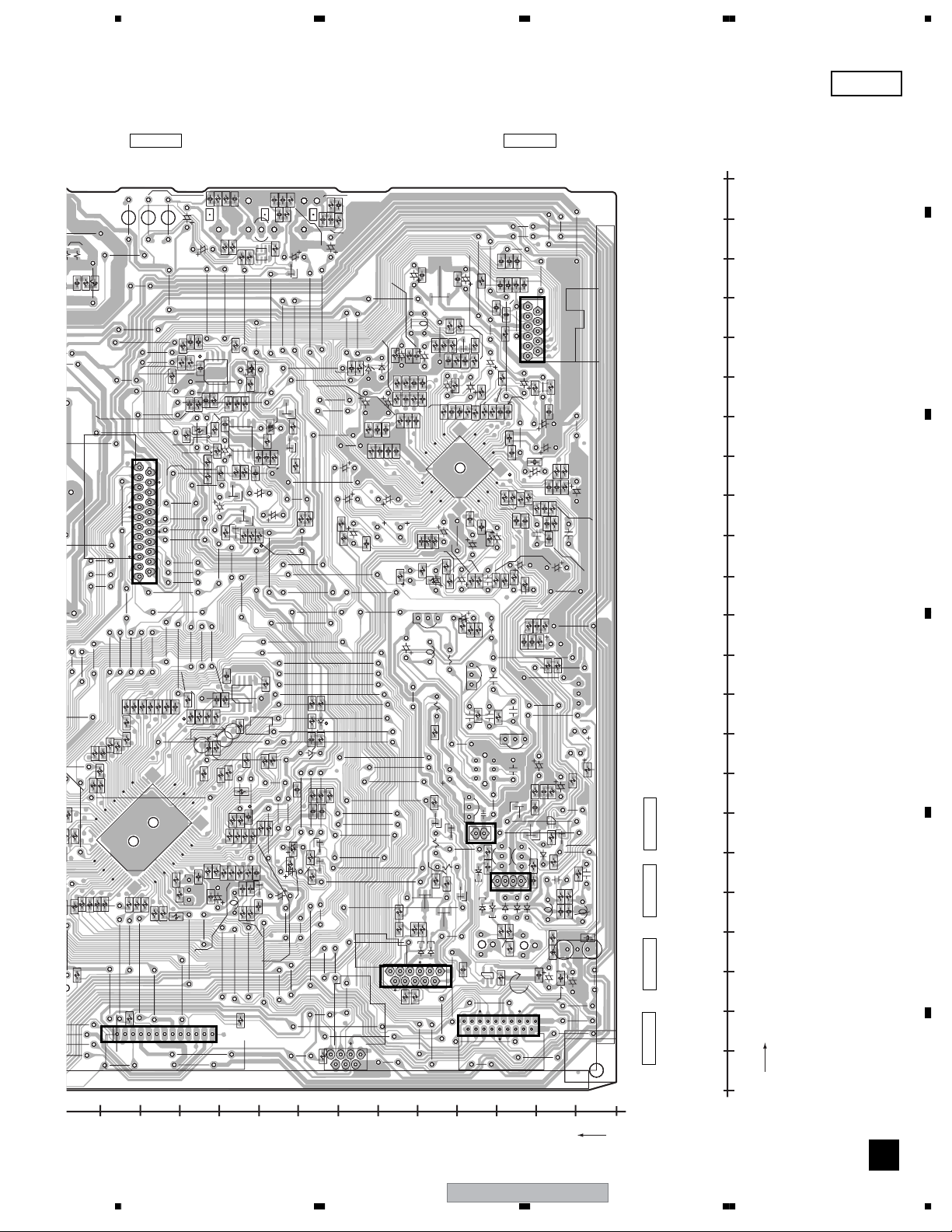
R5571
4
VE+5
5678
SIDE B
A
CN5505CN3004
230
R3040
IC5702
R7030
C1510
R2327
R2325
R5806
C5702
IC3001
R1504
R2816
Q5803
R5801
C3031
R1502
R5808
R7031
C3033
D5802
R2107
R3031
R5805
111
R3039
Q2101
R2102
R2104
R2103
C2101
R2101
C2102
R2105
C5721
R5701
C5703
R7029
R7019
33 48
32
64
1
C3011
R2312
C3012
R2322
C5718
R7032
R2402
R2404
R2328
R5702
16
R2403
C3020
C3025
17
C3015
C5717
1
R7028
11
R3034
C3032
R2321
C3034
C5720
R3032
C3016
R2311
C5719
C5716
R2401
C3017
C3027
C3022
C5707
C5706
C5705
GND
10 RDS
10
NC(VSM)
TXR
+9V
TXL
5 GND
D0
CLK
DI
1 CE
R3033
R3013
R3012
C3018
R3011
R2406
R2410
C2408
C2406
R2408
C2404
R2323
R2324
220
210
200
B
190
180
170
160
150
C
140
130
120
R2409
R2405
C2407
R2810
C2405
C2403
Q5802
R2301
C5901
VFDP
VFL+5
R2811
D2305
Q5805
Q5801
FLCS
FLCLK
5
1
R2809
R2802
D2301
15 FLDATA
1
GNDFL
C2301
MUSICLED
R2801
C2809
Q2303
Q2304
41
D2303
R2813
R2814
R2804
R5902
IC5901
FLAC2
KEY1
GNDLED
KEY2
10 FLAC1
MOVIELED
R2407
3
R7018
R7016
1
R2823
C2304
R2304
R2303
C2303
C5902
BIG
GNDU
VP+12
5 VE+5
JOG
R2821
C2302 R2302
119
REMOCON
1 TIMERLED
Q2352
R5901
L5901
C2811
C5905
R2351
R7027
NP
R2352
Q2351
R2824
R2822
C2812
C5906
CN2302
CN2301
CN5503
CN5504
110
100
90
80
70
60
50
40
30
20
10
D
E
0
Y
R3104
R3103
Q5603
C5613
Q5604
1
R2109
C2106
R1503
R1501
FLASH E/D
C3102
R5620
D5620
R5623
R5518
C3104
R3102
R3043
R5613
R5612
RECR
10 MOTOR
FLASH D0
5 FLASH CLK
7
C3106
R3051
C1509
R5814
RECF
VD+5
VE+5
XRESET
R2106
C3049
GNDMTC
GNDU
R2108
R3042
R3041
C3047
C3053
MODE
1 NC
5 HALF
C2104
R3030
C3043
R5813
PULSE
C3030R3029
C3052
NC
SOL
C3044C3029
R2354
1 GNDM
C3051
R5809
R5815
49
R2326
R2353
Q5804
D5801
R5816
R3001
C3001
R3002
C3073
C3072
R3078
R5551
R5550
STEST
R5537
C5514
R5516
HPR
10HPDET
R3061
R5549
30
R5517
R3003
IC3033
5
8
14
C3075
R3702
C5554
R5554
R5548
R5544
C5539
R5532
31
R5616
R5617
R5515
C5603
R5619
C5619
HPL
GNDHP
C3002
R3004
R3007
R3076
8
14
Q2106
C5540
1854
R5543
R5528
R5530
R5524
R5541
R3704
R3069
23
C3076
R5561
R5503
D+
R5560
51
GNDUSB
R3079
R5559
1
LINE(R)
R5507
R5504
GNDA
5MICSW
R5558
R5506
R3701
R3068
50
R5508
MIC
R3065
R5557
UTEST
R5513
R3703
C5555
VA+12V
GND
R3060
R3064
R5618
R3077
C3063
R5552
ECHOVOL
LINE(L)
R3465
R3467
C3461
C3463
R3463
R3083
R3084
C3070
R3075
R3080
R3073
C3071
R3074
SRIN
GNDD
SLIN
20 GNDA
SWIN
GNDA
CIN
GNDA
15 FRIN
GNDA
FLIN
VA-12
ABYPASS
10 MOIVE
MUSIC
FRTSURR
EDATA
ECLK
5 EXPWRM
VA+12
FR
GNDA
1 FL
1
R5562
R5563
R5566
R5567
R5568
R5570
R5581
R5596
R5603
5 XPROT
80
81
R5597
R5598
R5599
R5569
R5600
1 V+5USB
R5564
R5565
IC5501
100
R5501
R5611
D-
NP
5
R5523
R5626
Q2102
Q3001
R3005
R3070
IC5502
R5526
R5527
R5522
R5521
C5626
C3077
R5555
R5525
C5605
R5602
R5520
IC3032
R3067
R5610
C5604
C5601
R5601
R5519
R3063
R3062
C3074
Q2103
Q5601
C3101
C3067
C5622
R3101
C3062
R3066
Q3003
Q2105
R3081
R7026
C5614
R5608
R3006
Q2104
R3072
R8878
R3044
R5621
R5622
R5607
C3050
C5612
R5609
C3048
R7025
C3105
R3082
R5615
C3103
10
20304050607080901001101201300
XV-EV9
56
0
F
X
C
51
7
8
Page 52

1234
4.5 EVOL ASSY
A
B
C
D
E
SIDE A
D
EVOL ASSY
Y
0
0
X
10
2030405060708090100110120130140150160170180190
10
C8002
W812
1.FL
2.GNDA
3.FR
4.VA+12
5.EXPWRM
6.E-DATA
7.E-CLK
8.FRTSURR
9.MUSIC
10.MOVIE
11.ABYPASS
12.VA-12
13.FLIN
14.GNDA
15.FRIN
16.GNDA
17.CIN
18.GNDA
19.SWIN
20.GNDA
21.SLIN
22.GNDD
23.SRIN
W805
VA+12
CN8001
OPEN SIDE
W803
VA-1 2
1
23
W826
SRIN
R8002
W801
W825
VA-1 2
20
GNDA
W802
VA-1 2
W808
GNDD
W827
GNDD
W804
GNDD
W806
W807
R
GNDA
C8618
W815
C8601
W843
W823
IC8503
W907
W820
30
W813
R8001
VA+7
W824
W816
W821
C8001
VA+12
IC8501
SLIN
W814
W817
SIDE A
40
50
60
70
80
90
100
110
120
130
B
CONTACT SIDE
1
W851
W854
VA+7
W856
W882
C8217
W857
IC8407
W861
IC8406
W864
IC8405
C8715
PRODUCTION CODE
W855
GNDA
GNDA
W865
7
CN8002
W878
SL
SR
C
W880
VA-7
W881
VA+7
W902
W901
GNDA
IC8404
W891
VA+7
W895
W898
W887
C8637
C8518
C8707
W896
VA-7
W899
W900
W903
W904
W905
C8619
GNDA
W860
W859
W866
VA-1 2
C8620
W877
C8712
GNDA
W883
IC8403
W884
W886
GNDA
W888
W889
W893
W890
IC8502
C8713
W897
C8642
IC8504
CIN
IC8402
GNDA
W885
VA-7
W892
C8517
W868
W894
W869
C8701
W876
VA-7
VA+7
W831
W810
W809
W906
W837
VA-7
IC8401
W818
C8211
W838
W840
C8617
W908
C8608
C8604
W839
W841
C8612
GNDA
C8616
W819
W822
W829
FR
W833
VA+12
C8213
W842
W830
GNDA
W835
W862
C8613
W873
W874
GNDA
W849
C8214
W834
GNDA
GNDA
W846
W867
W875
W870
W847
W832
FL
W848
2.GNDA
W844
W871
C8215
W836
W872
C8714
W852
W853
W858
W863
VA-1 2
W845
VA+12
W850
C8216
VA+12
VA-1 2
4.GNDA
7.SR
6.GNDA
5.SL
1.C
3.SW
EVOL ASSY
XWK3261
XWK3260
CN8002
CN8001
CN903
C
CN3004
FCICT
KN2
KN1
(XNP3109-B)
F
D D
52
1234
XV-EV9
Page 53
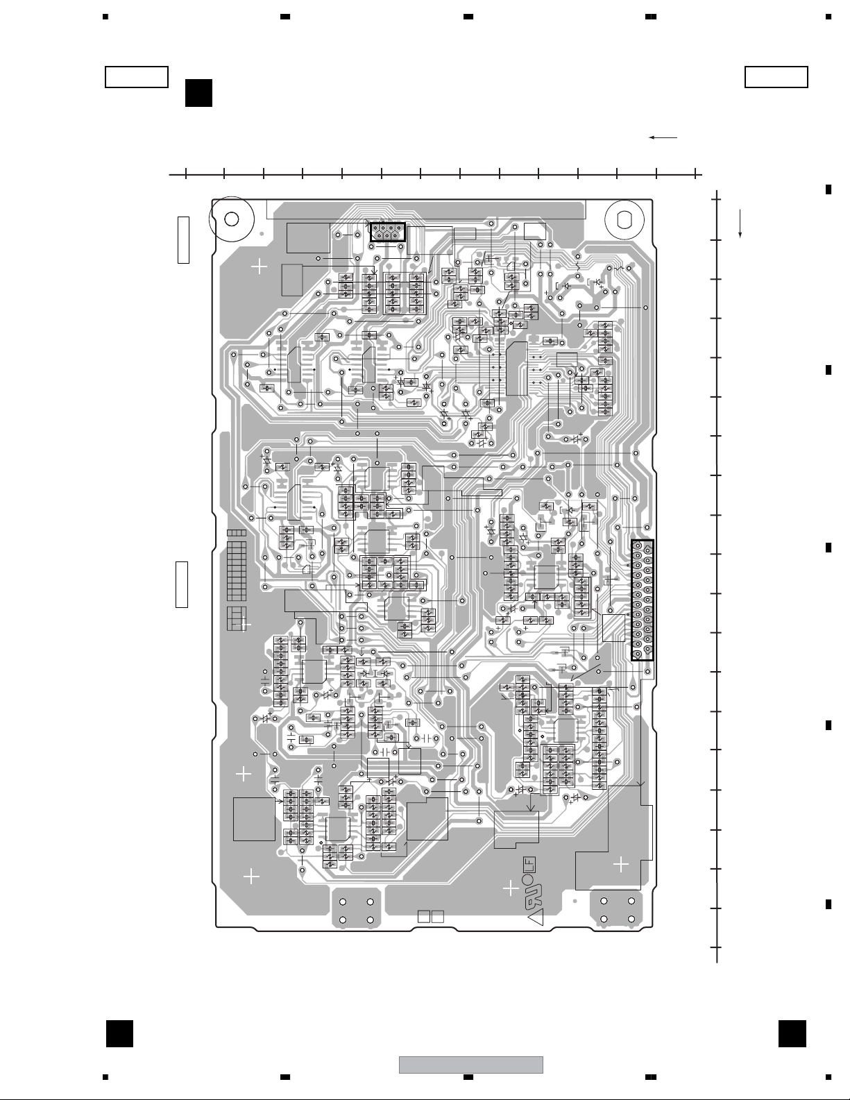
5678
SIDE B
D
EVOL ASSY
120
130
CN8002
C8202
VA-7
C8520
CBA
R8304
R8303
123456789
CN8001
1
0
0
123
0
C8638
C8639
C8640
C8641
C8648
C8649
1
0
C8705
C8706
R8704
R8703
C8708
C8709
R8702
C8703
C8704
GNDA
C8645
C8644
C8646
C8643
C8647
R8648
R8646
110
R8102
C8102
R8104
R8207
C8208
1
7
R8524
IC8404 R8523
1
1
7
VA+7
R8701
C8702
IC8403
GNDA
Q8303
C8513
C8512
C8503
R8518
5
7.SR
8
6.GNDA
VA+7
Q8304
NP
C8711
R8705
C8745
100
5.SL
4.GNDA
VA-7
814
GNDA
14
8
C8504
R8507
C8710
C8744
C8209
CIN
3.SW
R8101
C8101
C8519
R8706
R8708
R8707
R8709
R8710
IC8502
Q8701
5
8
C8656
R8649
R8663
2.GNDA
R8501
R8502
R8503
C8501
Q8401
1.C
GNDA
R8647
90
SL
SR
R8103
C8207
1
1
IC8402
7
1458
1
R8508
4
R8511
C8515
4
1
R8711
R8713
R8715
R8714
IC8504
1
R8659
R8658
80
7
VA+7
14
8
C8201
R8264
R8266
IC8407
IC8406
1458
R8721
D8703
IC8405
R8719
R8722
Q8402
VA-12
R8650
R8656
C8650
4
1
R8106
C8104
R8108
R8206
C8206
C9001
R8265
C8510
C8506
R8515
R8514
8
5
C8502
R8505
D8704
R8720
Q8702
C8747
C8746
R8712
R8716
R8718
R8717
VA-12
C8651
R8653
R8651
C8653
R8652
C8654
R8661
EVOL
ASSY
70
C8508
C8505
R8512
R8513
VA-1 2
60
R8105
R8268
C8103
R8269
R8107
R8205
C8205
GNDA
R8203
C8203
R8267
C8655
R8657
R8655
R8660
C8652
R8654
R8662
XWK3260
C9002
R8216
C8212
R8215
R8214
FR
C8511
C8509
C8514
C8507
C8516
GNDA
VA+12
C8609
R8611
R8617
R8516
R8618
R8510
C8615
GNDA
R8613
GNDA
R8506
R8509
R8619
R8504
GNDA
VA+12
XWK3261
C8004
R8521
C8614 C8605
R8612
C8610
R8614
R8615
R8630
C8627
R8665
50
C8204
R8204
Q8202
NP
R8201
R8202
R8263
120
1
R8262
IC8401
VA-7
R8213
R8260
R8628
R8725
R8724
R8624
C8623
R8623
C8621
R8723
C8624
R8621
C8622
R8622
VA+12
C8636
R8645
R8627
R8626
C8625
R8625
Q8201
R8261
R8640
R8641
R8637
R8639
C8632
R8212
R8208
C8210
5
8
R8209
R8602
Q8502
IC8501
R8609
C8607
R8616
R8629
C8626
R
40
D8001
R8210
R8211
VA+7
C8220
C8222
C8003
2140
VA+12
D8601
R8664
R8620
C8611
1
14
R8608
C8606
R8610
Q8306
Q8307
IC8503
1
1458
18.GNDA
19.SWIN
20.GNDA
21.SLIN
22.GNDD
23.SRIN
30
VA-12
GNDA
R8605
R8603
D8002
R8601
Q8501
GNDD
GNDD
R8631
GNDA
C8218R8217
C8226
R8220
C8221
R8221
C8223
C8224
C8225
VA-12
Q8305
R8604
C8602
C8603
R8606
R8607
R8644
R8643
R8642
C8635
SLIN
R8666
C8634
C8633
R8636
R8634
R8638
C8630
R8632
C8628
R8635
C8629
R8633
1.FL
2.GNDA
3.FR
4.VA+12
5.EXPWRM
6.E-DATA
7.E-CLK
8.FRTSURR
9.MUSIC
10.MOVIE
11.ABYPASS
12.VA-12
13.FLIN
14.GNDA
15.FRIN
16.GNDA
17.CIN
20
C8219
R8219
VA+12
C8631
R8218
23 1
SRIN
10
SIDE B
A
Y
0
X
0
10
2030405060708090100110120130140150160170180190
B
C
D
E
(XNP3109-B)
D D
56
XV-EV9
7
8
F
53
Page 54

1234
4.6 DISPLAY and HP/MIC ASSYS
A
B
C
D
SIDE A
140
130
120
110
100
90
80
70
60
50
40
30
20
10
E
DISPLAY ASSY
S5319
OPEN/CLOSE
S5318
LIST 3 REC
S5317
LIST 2
S5316
LIST 1
C5308
S5315
FUNCTION
V5301
FLAC2
W256
W219
VFDP
W222
W212
W213
W257
W208
C5317
GNDFL
W209
TUNING +
MS+/FF
S5320
VP+12
W216
W206
GNDFL
W268
W207
W214
IC5301
DISPLAY ASSY
D5303
D5304
D5302
S5321
PLAY/PAUSE
W243
W265
GNDFL
VFDP
W224
S5313
STOP
W260
XWZ4147
S5322
D5305
W245
W225
GNDFL
W246
GNDFL
TIMERLED
W226
W247
SIDE A
R
W269
TUNING -
MS-/FF
W230
VFDP
W231
C5301
S5314
W252
D5306
3 531 51
W232
W262
W263
GNDLED
W249
FLAC1
GNDFL
GNDU
W235
FLAC1
W234
VE+5
W253
ENTER
S5309
W259
S5308
STBY/ON
W241
W240
W237
W236
C5312
S5312
XBOOM
S5311
S5310
ASES
CN5301
15.FLDATA
13.MUSICLED
12.MOVIELED
W239
FLAC2
2.REMOCON
1.TIMERLED
IC5302
C5326
19.VFL+5
18.VFDP
17.FLCS
16.FLCLK
14.GNDFL
11.FLAC2
10.FLAC1
9.GNDLED
8.KEY1
7.KEY2
6.JOG
5.VE+5
4.VP+12
3.GNDU
19
W238
1
VE+5
SIDE
CONTACT
C
CN5504
CN5301
Y
0
(XNP3108-C)
140 150 160 170 180 190 200 210 220 230 240 250 260 270 280 290
X
70
E
60
50
40
30
F
HP/MIC ASSY
JA5401
C5443
C5405
GNDD
W330
W331
V+5USB
IC5401
C5416
W332
C5403
GNDD
C5413
GNDA
C5411
W336
C5406
XWZ4148
W333
R
VR5401
W334
VA+12
HP ASSY
W312
JA5402
C5428
GNDA
W314
W335
W318
HPL
GNDHP
HPR
W329
W320
GNDHP
W323
W321
HPDET
ECHOVOL
VA+12V
GNDA
MIC SW
GNDD
V+5USB
MIC
13
D+
D-
W327
5401
J
1
JA5403
GNDA
C5430
GNDA
IC5402
JA5404
C5421
C5433
20
(XNP3108-C)
F
10
Y
10
0
20 30 40 50 60 70 80 90 100 110 120 130 140 150
X
E F E F
54
1234
XV-EV9
J5401
C
CN3301
Page 55

5678
SIDE B
19.VFL+5
18.VFDP
17.FLCS
16.FLCLK
15.FLDATA
14.GNDFL
13.MUSICLED
12.MOVIELED
11.FLAC2
10.FLAC1
9.GNDLED
8.KEY1
7.KEY2
6.JOG
5.VE+5
4.VP+12
3.GNDU
2.REMOCON
1.TIMERLED
CN5301
VE+5
F
119
E
DISPLAY ASSY
S5312
XBOOM
R5312
REC
S5311
R5311
S5310
ASES
R5310
VE+5
S5309
ENTER
R5309
GNDLED
STBY/ON
A
C5318
FLAC1
C5310
D5301
C5327
R5322
R5323
C5328
E
R5313
R5339
VFDP
R5338
S5314
L5302
C5311
R5314
TUNING -
MS-/FF
Q5304
D5309
GNDFL
GNDLED
C5306
L5301
R5328
R5329
Q5303
FLAC1
TIMERLED
Q5302
GNDFL
R5327
R5326
D
C5330
C5302
C5303
R5325
C5305
C5304
C5307
R5335
R5334
R5302
R5321
14
GNDFL
R5324
R5304
R5303
SIDE B
A
OPEN/CLOSE
S5313
STOP
S5319
R5319
R5318
C
R5337
R5336
S5321
PLAY/PAUSE
113
26
C5329
GNDFL
C5324
27
S5318
S5320
GNDFL
Q5308
R5343
R5349
R5350
Q5301
R5342
Q5306
Q5307
R5317
S5315 S5308
FUNCTION
C5316
C5314
FLAC1
DISPLAY ASSY
XWZ4147
R5320
TUNING +
R5346
VP+12
R5344
B
R5307
R5308
R5347
MS+/FF
R5306
R5348
R
C5320
C5321
C5322
FLAC1
39
IC5301
GNDFL
Q5309
40
R5345
C5319
52
LIST 3
S5316
C5315
Q5305
R5316
R5315
C5313
R5353
R5341
R5354
R5351
H
S5317
LIST 2
LIST 1
FLAC2
R5340
R5352
140
130
120
110
100
90
80
70
60
50
40
30
20
B
C
G
10
0
(XNP3108-C)
140150160170180190200210220230240250260270280290
X
70
60
50
40
30
20
J5401
F
HP/MIC ASSY
R5404
C5420
R5409
C5419
R5416
C5408
C5409
C
L3903
C3903
R3908
R3904
12.GNDHP
L3901
R3913
L3902
13.HPL
11.HPR
10.HPDET
9.ECHOVOL
C3904
R3914
R3909
R3915
R5424
C3921
C5427
R5427
R5425
C3905
R5426
C3920
C3919
C5431
R5423
C5424
8
9
C5429
R5421
R5422
C5422
IC5402
C5432
C5423
D5404
1
R5418
R5419
L5403
16
C5426
C5425
R5417
R3903
R3907
13
10
8.VA+12V
7.MIC
6.GNDA
5.MIC SW
4.GNDD
1
3.D+
2.D-
1.V+5USB
HP ASSY
R5412
R5403
C5414
C5415
R5413
R5402
XWZ4148
R5405
R
B
R5411
C5412
R5406
R5448
C5407
5
C5417
R5415
R5410
C5404
C5402
R5401
C5410
14
C5439
L5405
IC5401
8
R5414
A
R5439
C5442
R5440
R5444
L5407
R5441
C5440
C5441
D5401
R5442
(XNP3108-C)
2030405060708090100110120130140150
10
0
10
X
E F E F
56
XV-EV9
7
8
Y
Y
D
E
F
55
Page 56

1234
3
4.7 PRIMARY ASSY
SIDE A
G
A
PRIMARY ASSY
250
240
230
LIVE
AN1
H1
FU1
RISK OF FIRE
B
220
210
KN2
200
190
REPLACE FUSE AS MARK
NEUTRAL
W128
S1
C1
H2
L1
W130
STBY
W116
W117
W115
W114
W145R1W144
H4
FU2
W131
W129
H3
W146
W147
PRODUCTION CODE
W132
H5
W133
W120
FU3
H6
W150
W151
W164
W165
180
C
170
160
W134
W135
MTXJ ONLY
W142
STBY
W137
W143
W140
W141
W136
FCICT
W152
W153
W154
W155
PRIMARY ASSY
150
140
PRIMARY
D
130
XWZ4146
XWZ4150
W156
W157
12 1
CN1
120
R
110
100
W125
W124
ALL
90
E
W168
80
W122
W169
MTXJ ONLY
W123
W113
W110
W109
ALL
W108
STBY
W138
W105
W106
CN2
4
ALL
70
60
Y
(XNP3108-C)
20 30 40 50 60 70 80 90 100 110 120 1
10
0
F
X
G
56
1234
XV-EV9
Page 57
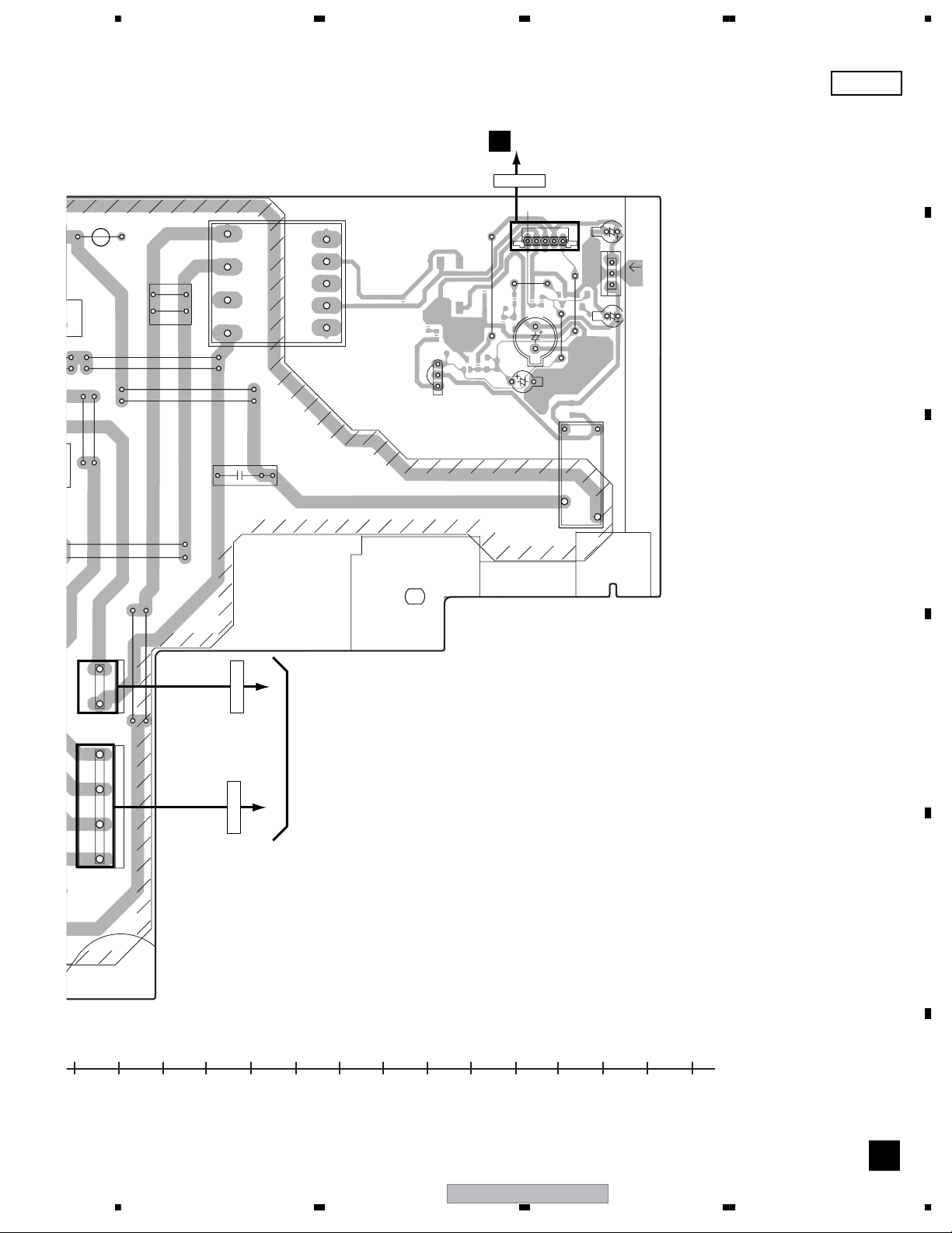
CN1
CN2
H5
W133
FU3
W164
W165
W120
W150
W151
W104
W107
STBY
5678
SIDE A
A
J12
C
CN3
SUBAC
VE+5
XPROT
SYSPOW
T2
W148
W149
1
CN3
W161
W159
VE+5
Q2
VE+5
GNDU
C7
5
C5
SIDE
IC1
C4
W163
W162
C2
TA7805S
PRINTED
B
SECONDARY
RY81
C3
C
W152
W153
W156
W157
12 1
CN1
TRANSFORMER
(T1)
D
CN2
4
E
10 120 130 140 150 160 170 180 190 200 210 220 230 240 250
XV-EV9
56
7
F
G
57
8
Page 58

A
B
SIDE B
1234
G
PRIMARY ASSY
CN3
GNDU
SUBAC
SYSPOW
XPROT
VE+5
C6
OUT
IN
D3
Q1
R3
R5R2R4
D2
1
0
123456789
0
0
123
1
0
D1
2
3
C9
R8
D5
4
1
R7
Q3
R6
R9
A
B
C
C8
TX WINDING
FU3
D4
SECONDARY
C
12
D
CN1
1
CN2
4
E
TX WINDING
110120130140150160170180190200210220230240250
F
G
58
1234
XV-EV9
Page 59

5678
SIDE B
A
250
TX WINDING
240
FU3
FU2
FU1
RISK OF FIRE
REPLACE FUSE AS MARK
LIVE
NEUTRAL
230
220
210
200
190
180
170
160
B
C
PRIMARY ASSY
XWZ4146
150
XWZ4150
12
PRIMARY
140
D
130
1
4
TX WINDING
R
(XNP3108-C)
10
2030405060708090100110120
XV-EV9
56
120
110
100
90
80
70
Y
60
0
X
E
F
G
59
7
8
Page 60

1234
4.8 AMP ASSY
SIDE A SIDE A
A
AMP ASSY
I
1
1
W157
CN3651
1
W133
VH+
VL-
VL+
W114
W130
W135
19
word surface
1
119
W129
W124
C3653
D82
IC81
TA7805S
W122
W121
Word Surface
Q91
2SJ304
C3661
C3662
C3663
C3401
C3402
C3501
FROUT
W131
IC3301
W126
VA-12
W125
W109
D98
C3301
C3302
W213
W108
D3653
W107
C98
C91
C3502
C3311
UN+8
W110
W123
C82
SWOUT
W113
W232
D3652
SLOUT
W111
W112
DC
FC
LF
W106
C3317
C3318
C3168
C3178
23
231
1
23
231
Production Code
W103
W212
W102
C3179
C3167
PNE-1B1
W101
CN3001
CN3002
CN3651
CN3001
CN3002
AMP ASSY
(XNP3088-D)
-Vcc
W201
W200
9
3
3
W197
D3421
R3418
C3408
C3507
R3517
2
C102
W190
C3407
VL+
W176
C101
W188
W168
W189
W210
D3391
W169
D3386
D3387
W180
R3422
D3422
W162
D3388
D3385
GNDP
GNDP
W178
R3327
+Vcc
W177
GNDP
VF-12
XPROTECT
VP+12
VPF+12
VD+5
VA-12
D3424
W165
W211
W163
VL-
W183
R3328
W174
W179
-Vcc
W167
C3423
W223
W196
W195
W222
W185
C3321
C3322
W194
W193
W192
W173
D3426
W184
W220
W224
GNDREG
W216
W221
D3327
W172
W144
D3427
W253
W143
C3422
C3421
W215
W152
D3324
D3326
R3427
C3424
D3328
C3323
R3322
Q3654
C3651
GNDS
GNDP
W141
D3428
W219
W218
W226
C3324
W255
R3657
W138
R3518
W154
R3318
D3322
FROUT
W171
Q3655
Q3656
VH+
SROUT
W153
R3317
W150
W149
D3655
C3652
W142
W170
W140
R3428
Q3657
W203
R3388
W256
D3605
D3390
2SK2232
B
D3389
W240
2SJ304
D3604
W234
Surface
Word
C72
W241
D3603
W242
TA79012S
C
D
E
20 30 40 50 60 70 80 90 100 110 120 130 140 150 160 170 180
D3602
W206
TA7812S
W243
D3601
W225
C63
R85
W208
119
1
W205
STK433-070
STK433-270
W204
19
word surface
IC3401
C3312
Q3384
Q3383
IC71
W207
IC61
Q62
D3394
R3387
D3393
D72
D63
W209
W202
W199
W198
D3425
W187
+Vcc
W175
W181
D3423
D
VL-
VL+
R3421
R3417
W252
W151
D3323
W145
W148
SWOUT
C3508
C3308
C3307
R3321
W147
C3680
C3673
W115
W156
FLOUT
C3674
W251
W146
W116
W155
W254
W127
W118
W117
VH-
D3321
D3325
D3654
D3651
W214
X
To FAN
CN3022
H
CN3021
H
120
110
100
90
80
70
60
50
40
30
20
10
F
I I
60
1234
XV-EV9
0
Y
Page 61

5678
SIDE B SIDEB
AMP ASSY
I
CN3651
CN3001CN3002
(XNP3088-D)
VHVHSROUT
SROUT
GNDP
GNDP
SLOUT
SLOUT
GNDS
COUT
COUT
VH+
VH+
SWOUT
SWOUT
VL+
VL+
FROUT
FROUT
VL-
VL-
FLOUT
FLOUT
23 1
RYRC
GNDF
UN+8
UN+8
GNDR
GNDR
XPRCT
VD+5
VA-12
VP+12
VFL+5
RYFS
MUTEC
MUTE
VPR+8
VPR+8
FLIN
GNDA
FRIN
SWIN
CIN
SLIN
SRIN
23 1
PNE-1B1
R3504
R3403
R3500
Q3502
Q3504
SLOUT
SWOUT
CBA
LF
123456789
0
1
1
123
0
0
0
C97
R96
R97
R3372
R3313
R3371
R3303
R3373
R3314
R3514
R3374
R3404
Q3401
R3414
Q3501
R3503
R3393
R3395
UN+8
R94
R3687
VH+
Q3301
R3413
R3394
D3301
VA-12
VL-
VL+
C3310
FROUT
R3396
R3351
R108
R95
R48
C92
R3304
R3513R3501
VH-
C3510
R3512
R3312
Q3385
119
IC3301
C81
IN
S
D
R92
Q92
R93
R3678
C3676
R3673
R3302
R3664
R3663
R3502
R3666
R3665
C3678
R3679
R3674
R3401
R3402
XWK3262
XWK3263
C3506
C3504
R3324
1
R114
OUT
TH111
R46
Q43
G
R47
R3301
C3677
5
IC3305
8
XWK3188
XWK3202
XWK3203
FAN SIDE
SROUT
R3510
R3592
R3508
R3310
R3308
C3304
C3306
C3309
R3311
R3391
C3305
R3307
R3323
D3657
R3658
D42
Q3652
R113
R111
R112
R45
Q111
Q121
R123
TH121
R121
R122
R91
D91
R3661
R3662
Q3660
R3677
41
R3667
R3668
R3681
R3676
R3506
R3309
C3303
R3305
B1E1
C2
R3306
VH+
D3381
D3582
Q3653
FLOUT
GNDS
R3669
R3682
SWOUT
C1
B2
E2
R3392
R3656
Q3651
FROUT
GNDREG
GNDP
GNDP
R3683
C3679
R3675
R3680
D3382
R3651
GNDP
R3654
C3426
R3655
D3658
VP+12
VPF+12
VD+5
VA-12
VL-
+Vcc
C3326
R3326
VF-12
XPROTECT
D3482
C3671
1
4
R3426
GNDP
GNDP
GNDP
-Vcc
R3492
IC3304
R3382
R3381
8
VL+
5
VL-
R105
D102
R106
NP
D106
R3405
C3403
R3409
D3481
VL+
Q104
R3671
R3406
R3672
C3672
R3505
-Vcc
R3407
C3405
R3491
NP
R3410
R3408
R104
+Vcc
Q103
R3496
Q3485
C71
R3423
Q3382
R3385
Q3381
R3386
Q102
R101
Q101
R68
C62
R3383
IN
OUT
C61
R64
R65
R67
R3451
R3424
C3406
C3404
C3503
C3505
R3507
R3509
D3401
R3494
R3495
R3493
R3384
R103
R3389
R109
R3411
C3409
R3591
IC3401
IN
OUT
119
R3390
G
D
S
D105
GDS
D101
R102
C66
Q63
R66
R63
R61
R62
C3410
R3412
R3511
C3509
D3581
20 30 40 50 60 70 80 90 100 110 120 130 140 150 160 170 180
X
A
B
C
D
E
0
Y
10
20
30
40
50
60
70
80
90
100
110
120
I I
56
XV-EV9
7
8
F
61
Page 62

1234
5. PCB PARTS LIST
NOTES:
A
B
Parts marked by "NSP" are generally unavailable because they are not in our Master Spare Parts List.
The mark found on some component parts indicates the importance of the safety factor of the part.
Therefore, when replacing, be sure to use parts of identical designation.
When ordering resistors, first convert resistance values into code form as shown in the following examples.
Ex.1 When there are 2 effective digits (any digit apart from 0), such as 560 ohm and 47k ohm (tolerance is shown by J=5%,
and K=10%).
560 Ω
47k Ω
0.5 Ω
1 Ω
Ex.2 When there are 3 effective digits (such as in high precision metal film resistors).
5.62k Ω
Meaning of the figures and others in the parentheses in the parts list.
Example) IC 301 is on the point (face A, 91 of x-axis, and 111 of y-axis) of the corresponding
PC board.
IC 301 (A, 91, 111) IC NJM2068V
56 x 10
47 x 10
R50
1R0
1
3
Mark No. Description Part No.
LIST OF ASSEMBLIES
LIST OF ASSEMBLIES
NSP 1..DVD ASSY XXA3039
2..DVDM ASSY AWM8059
NSP 2..06 LOADER ASSY VWT1226
3..LOAB ASSY VWG2346
NSP 1..MAIN ASSY (DDRXJ, DLXJ) XWK3254
C
NSP 1..MAIN ASSY (DDXJ/RB) XWK3255
NSP 1..MAIN ASSY (MTXJ) XWK3256
NSP 1..EVOL ASSY XWK3261
561
473
1
5621
RD1/4PU J
RD1/4PU J
RN2H K
RS1P K
RN1/4PC F562 x 10
561
473
R50
1R0
5621
Mark No. Description Part No.
NSP 1..SUB ASSY XWK3320
(DDRXJ, DLXJ, DDXJ/RB)
NSP 1..SUB ASSY (MTXJ) XWK3321
2..DISPLAY ASSY XWZ4147
2..HP/MIC ASSY XWZ4148
2..PRIMARY ASSY XWZ4146
(DDRXJ, DLXJ, DDXJ/RB)
2..PRIMARY ASSY (MTXJ) XWZ4150
2..TRADE ASSY XWZ4149
NSP 1..AMP UNIT 6CH XXQ3007
2..6CH AMP ASSY XWK3262
1..FM/AM TUNER UNIT AXX7211
7777 CONTRAST OF PCB ASSEMBLIES
MAIN ASSY
C
D
XWK3255, XWK3256 and XWK3254 are constructed the same except for the following:
Mark Symbol and Description XWK3254 XWK3255 XWK3256
R5616 RS1/16S103J RS1/16S393J RS1/16S103J
R5617 Not used RS1/16S683J RS1/16S103J
PRIMARY ASSY
G
XWZ4150 and XWZ4146 are constructed the same except for the following:
Mark Symbol and Description XWZ4146 XWZ4150
> S1 VOLTAGE SELECTOR XKX3001 Not used
E
7777 PCB PARTS LIST FOR XV-E9/DDRXJ UNLESS OTHER WISE NOTED
Mark No. Description Part No.
LOAB ASSY
A
MISCELLANEOUS
S 101 VSK1011
CN602 CONNECTOR S2B-PH-K
CN601 CONNECTOR S5B-PH-K
F
Mark No. Description Part No.
DVDM ASSY
B
MISCELLANEOUS
IC 101 (A,62,106) 6CH DRIVER IC BD7995EFS
IC 201 (A,50,44) DVD IC MT1389FE/H-L
IC 202 (B,34,25) SD-RAM(64M) HY57V641620ETP-H
IC 203 (B,34,54) FLASH ROM AYW7132
FLASH MEMORY IC S29AL016D70TFI010
IC 204 (A,19,44) EEPROM S-24CS64A0I
62
XV-EV9
1234
Page 63

5678
Mark No. Description Part No.
IC 401 (B,92,22) DVD VIDEO AMP IC MM1758XF
>
IC 711 (A,33,74) REGULATOR (1.8V) MM1661JH
>
IC 731 (A,29,92) DC/DC CONTROLLER IC R1224N102H
>
IC 751 (A,32,113) REGULATOR IC (5.0V) MM1565AF
>
IC 761 (A,41,119) REGURATOR (ADJ.) BA3948FP
Q 304 (A,77,127) TRANSISTOR 2SC4081
Q 305 (A,83,125) NMOS FET TRANSISTOR UM5K1N
Q 307 (A,71,87) CHIP TRANSISTOR HN1A01F
Q 308 (A,63,87) CHIP TRANSISTOR HN1A01F
Q 481 (A,103,7) CHIP TRANSISTOR DTC114YUA
Q 501 (A,105,53) TRANSISTOR 2SD2114K
Q 502 (A,96,53) TRANSISTOR 2SD2114K
Q 504 (A,111,67) CHIP TRANSISTOR DTC114YUA
Q 505 (A,99,49) TRANSISTOR 2SA1576A
Q 531 (A,103,76) TRANSISTOR 2SD2114K
Q 532 (A,95,76) TRANSISTOR 2SD2114K
Q 534 (A,106,90) CHIP TRANSISTOR DTC114YUA
Q 535 (A,109,77) TRANSISTOR 2SA1576A
Q 561 (A,101,99) TRANSISTOR 2SD2114K
Q 562 (A,92,99) TRANSISTOR 2SD2114K
Q 564 (A,106,114) CHIP TRANSISTOR DTC114YUA
Q 565 (A,106,98) TRANSISTOR 2SA1576A
Q 701 (A,24,134) TRANSISTOR 2SA1576A
Q 702 (A,27,129) DIGITAL TRANSISTOR DTC124EUA
>
Q 732 (B,22,90) FET RSQ035P03
Q 801 (A,46,94) DIGITAL TRANSISTOR DTC124EUA
Q 821 (A,39,85) TRANSISTOR 2SA1576A
Q 851 (A,39,92) TRANSISTOR 2SA1576A
Q 881 (B,36,100) TRANSISTOR 2SA1576A
D 731 (A,29,87) DIODE 1SS355
D 732 (B,18,92) DIODE RSX201L-30
D 733 (A,24,94) DIODE 1SS355
D 801 (A,46,92) DIODE UDZS4R7(B)
D 821 (A,42,86) DIODE 1SS355
D 851 (A,42,94) DIODE 1SS355
D 852 (A,39,89) DIODE 1SS355
D 861 (A,45,86) DIODE 1SS355
D 862 (A,44,86) DIODE 1SS355
D 881 (B,40,99) DIODE 1SS355
L 731 (A,23,109) POWER INDUCTOR(22U) DTL1099
L 732 (A,22,84) POWER INDUCTOR ATH7011
L 751 (A,34,99) INDUCTOR CTF1395
L 761 (A,41,78) COIL VTH1047
L 901 (B,39,130) INDUCTOR CTF1334
X 201 (A,76,48) CRYSTAL RESONATOR VSS1172
CN101 (A,88,140) CONNECTOR CKS5045
CN102 (A,69,142) 12P CONNECTOR AKN7031
CN103 (A,103,139) 04P CONNECTOR RKN1045
CN104 (A,93,9) CONNECTOR AKM1291
CN901 (A,42,142) 27P CONNECTOR VKN1319
CN902 (A,116,28) 27P CONNECTOR VKN1319
CN903 (A,116,101) 7P CONNECTOR VKN1299
RESISTORS
R 131 (A,61,95) RS1/10S4R7J
R 132 (A,63,95) RS1/10S4R7J
R 133 (A,65,95) RS1/10S4R7J
R 134 (A,66,95) RS1/10S4R7J
R 135 (A,68,95) RS1/10S4R7J
R 136 (A,70,95) RS1/10S4R7J
56
Mark No. Description Part No.
R 151 (A,59,117) RS1/10S1R0J
R 152 (A,59,121) RS1/10S1R8J
R 153 (A,57,117) RS1/10S1R0J
R 154 (A,57,121) RS1/10S1R8J
R 201 (A,51,68) RS1/16S152J
R 202 (A,49,68) RS1/16S223J
R 204 (A,48,68) RS1/16S223J
R 205 (A,46,68) CHIP RESISTOR RS1/16S5102F
R 206 (A,45,68) CHIP RESISTOR RS1/16S5102F
R 208 (B,28,72) RS1/10S0R0J
R 212 (B,42,59) RS1/16S103J
R 213 (B,43,59) RS1/16S103J
R 218 (A,17,39) RS1/16S103J
R 219 (A,17,36) RS1/16S103J
R 220 (B,29,41) RS1/16S333J
R 221 (A,27,44) CHIP RESISTOR ARRAY RAB4C330J
R 223 (B,27,39) RS1/16S330J
R 224 (A,31,49) RS1/16S330J
R 225 (A,37,24) RAB4CQ330J
R 226 (A,39,24) RS1/16S330J
R 227 (A,41,24) RS1/16S330J
R 229 (A,38,20) RS1/16S330J
R 230 (A,76,34) RS1/16S103J
R 233 (B,42,49) RS1/16S0R0J
R 235 (B,27,46) RS1/16S472J
R 237 (B,72,39) RS1/16S102J
R 248 (B,54,40) RS1/16S330J
R 249 (B,72,40) RS1/16S102J
R 251 (A,70,49) RS1/16S104J
R 252 (A,68,48) RS1/16S0R0J
R 253 (A,70,47) RS1/16S681J
R 254 (B,58,49) RS1/16S754J
R 255 (B,58,54) RS1/16S104J
R 256 (A,72,58) RS1/16S153J
R 259 (A,21,37) RS1/16S330J
R 260 (A,21,36) RS1/16S330J
R 261 (B,29,37) RS1/16S330J
R 279 (A,67,30) CHIP RESISTOR RS1/16S2201F
R 281 (B,20,23) RS1/10S0R0J
R 284 (A,34,61) RS1/16S103J
R 313 (A,80,125) RS1/16S104J
R 314 (A,75,125) RS1/16S103J
R 315 (A,80,128) RS1/16S103J
R 318 (A,80,126) RS1/16S104J
R 321 (A,61,87) RS1/16S4R7J
R 322 (A,68,87) RS1/16S4R7J
R 325 (A,73,87) RS1/16S4R7J
R 326 (A,66,87) RS1/16S4R7J
R 401 (A,82,30) RS1/16S103J
R 402 (B,99,14) RS1/16S103J
R 403 (B,99,13) RS1/16S0R0J
R 404 (A,83,25) RS1/16S102J
R 411 (A,73,20) RS1/16S1500F
R 412 (A,71,20) RS1/16S1500F
R 413 (A,74,20) RS1/16S1500F
R 414 (A,70,20) RS1/16S1500F
R 415 (A,68,20) RS1/16S1500F
R 416 (A,67,20) RS1/16S1500F
R 421 (B,102,15) RS1/16S0R0J
R 422 (B,99,20) RS1/16S0R0J
XV-EV9
7
A
B
C
D
E
F
63
8
Page 64

1234
Mark No. Description Part No.
R 423 (B,99,21) RS1/16S0R0J
R 424 (B,99,23) RS1/16S0R0J
R 425 (B,99,25) RS1/16S0R0J
R 426 (B,99,29) RS1/16S0R0J
A
Mark No. Description Part No.
R 737 (A,31,83) RS1/16S2702F
R 738 (A,29,82) RS1/16S1502F
R 739 (A,19,78) RS1/16S0R0J
R 740 (A,29,85) RS1/16S0R0J
R 481 (A,103,9) RS1/16S102J
R 500 (B,101,72) RS1/16S0R0J
R 511 (A,102,57) RS1/16S223J
R 512 (A,99,57) RS1/16S223J
R 513 (A,105,56) RS1/16S471J
R 514 (A,97,56) RS1/16S471J
R 515 (A,101,53) RS1/16S222J
R 516 (A,100,53) RS1/16S222J
R 517 (B,109,66) RS1/16S102J
R 518 (A,102,49) RS1/16S102J
B
R 519 (A,101,47) RS1/16S103J
R 521 (A,110,48) RS1/16S0R0J
R 522 (A,112,48) RS1/16S0R0J
R 523 (B,105,66) RS1/16S0R0J
R 524 (B,105,68) RS1/16S0R0J
R 530 (A,86,91) RS1/16S0R0J
R 541 (A,101,80) RS1/16S223J
R 542 (A,97,80) RS1/16S223J
R 543 (A,103,80) RS1/16S471J
R 544 (A,95,80) RS1/16S471J
C
R 545 (A,100,77) RS1/16S222J
R 546 (A,99,77) RS1/16S222J
R 547 (B,103,89) RS1/16S102J
R 548 (A,112,78) RS1/16S102J
R 549 (A,112,76) RS1/16S103J
R 750 (A,34,97) RS1/16S0R0J
R 751 (A,33,119) RS1/16S0R0J
R 761 (A,36,114) RS1/16S0R0J
R 762 (A,45,114) RS1/16S3902F
R 763 (A,44,112) RS1/16S334J
R 764 (A,44,110) RS1/16S334J
R 767 (A,43,72) RS1/16S153J
R 768 (A,40,72) RS1/16S153J
R 769 (A,42,74) RS1/16S330J
R 770 (A,41,74) RS1/16S330J
R 801 (A,48,87) RS1/16S471J
R 821 (A,37,88) RS1/16S103J
R 822 (A,36,85) RS1/16S473J
R 823 (A,35,85) RS1/16S153J
R 824 (A,34,85) RS1/16S103J
R 851 (A,36,92) RS1/16S473J
R 852 (A,35,92) RS1/16S103J
R 853 (A,33,92) RS1/16S103J
R 881 (B,36,97) RS1/16S473J
R 882 (B,36,93) RS1/16S103J
R 901 (A,39,128) RS1/16S0R0J
R 902 (B,39,132) RS1/10S0R0J
R 903 (A,46,129) RS1/16S332J
R 904 (B,45,129) RS1/16S682J
R 905 (A,47,129) RS1/16S332J
R 551 (A,112,92) RS1/16S0R0J
R 552 (A,110,92) RS1/16S0R0J
R 553 (B,100,88) RS1/16S0R0J
R 554 (B,100,90) RS1/16S0R0J
R 560 (B,97,112) RS1/16S0R0J
R 571 (A,98,104) RS1/16S223J
D
R 572 (A,95,104) RS1/16S223J
R 573 (A,101,103) RS1/16S471J
R 574 (A,93,103) RS1/16S471J
R 575 (A,98,99) RS1/16S222J
R 576 (A,97,99) RS1/16S222J
R 577 (B,103,110) RS1/16S102J
R 578 (A,107,94) RS1/16S102J
R 579 (A,108,98) RS1/16S103J
R 581 (A,110,102) RS1/16S0R0J
R 582 (A,110,104) RS1/16S0R0J
R 583 (B,100,113) RS1/16S0R0J
E
R 584 (B,100,112) RS1/16S0R0J
R 590 (B,90,51) RS1/16S0R0J
R 596 (B,96,46) RS1/16S0R0J
R 597 (B,95,49) RS1/16S0R0J
R 598 (B,92,48) RS1/16S0R0J
R 602 (B,107,126) RS1/16S682J
R 604 (B,105,126) RS1/16S103J
R 701 (A,24,137) RS1/16S473J
R 702 (A,27,134) RS1/16S103J
R 732 (A,25,91) RS1/10S100J
R 733 (A,25,93) RS1/16S220J
F
R 734 (A,29,88) RS1/16S473J
R 735 (A,29,84) RS1/16S272J
R 736 (A,31,92) RS1/16S1802F
64
1234
R 906 (B,47,129) RS1/16S682J
R 907 (A,49,129) RS1/16S471J
R 908 (A,50,129) RS1/16S332J
R 909 (B,50,129) RS1/16S682J
R 910 (A,52,129) RS1/16S221J
R 911 (A,53,129) RS1/16S221J
R 912 (A,55,129) RS1/16S0R0J
R 916 (B,49,129) RS1/16S223J
R 917 (B,52,129) RS1/16S223J
R 921 (A,106,7) RS1/16S0R0J
R 922 (A,106,8) RS1/16S0R0J
R 923 (A,106,10) RS1/16S0R0J
R 924 (A,106,11) RS1/16S0R0J
R 1001(B,107,6) RS1/10S0R0J
R 1002(B,116,16) RS1/10S0R0J
R 1003(B,118,16) RS1/10S0R0J
CAPACITORS
C 101 (A,52,119) CEVW101M16
C 102 (A,73,101) CKSRYB105K10
C 103 (A,66,116) CKSRYB105K10
C 104 (A,61,117) CKSRYB105K10
C 121 (B,61,112) CKSRYB105K10
C 131 (A,52,103) CKSRYB104K25
C 140 (A,63,137) CKSRYB105K10
C 144 (A,62,99) CKSRYB222K50
C 145 (A,64,98) CKSRYB222K50
C 146 (A,60,98) CKSRYB222K50
C 151 (A,68,114) CKSRYB103K50
C 152 (A,71,114) CKSRYB103K50
C 153 (A,73,111) CKSRYB103K50
XV-EV9
Page 65

5678
Mark No. Description Part No.
C 161 (A,58,96) CKSRYB102K50
C 200 (B,51,54) CKSRYB104K25
Mark No. Description Part No.
C 265 (B,58,53) CCSRCH220J50
C 266 (B,65,52) CKSRYB104K25
C 201 (A,21,52) CHIP ELECT.CAPACITOR CEVW221M4
C 202 (B,68,61) CHIP ELECT.CAPACITOR CEVW221M4
C 203 (A,56,78) CHIP ELECT.CAPACITOR CEVW470M16
C 204 (B,52,59) CKSRYB104K25
C 205 (B,50,59) CKSRYB104K25
C 206 (A,48,77) CHIP ELECT.CAPACITOR CEVW470M16
C 207 (B,53,54) CKSRYB104K25
C 208 (A,49,72) CKSRYB222K50
C 209 (A,51,72) CKSRYB104K25
C 210 (A,48,72) CKSRYB222K50
C 211 (A,46,72) CCSRCH101J50
C 212 (A,45,72) CCSRCH101J50
C 213 (B,51,63) CKSRYB104K25
C 215 (B,52,68) CHIP ELECT.CAPACITOR CEVW470M16
C 216 (B,45,59) CKSRYB103K50
C 217 (B,43,54) CKSRYB104K25
C 218 (B,45,58) CKSRYB102K50
C 219 (B,46,53) CKSRYB562K50
C 220 (A,31,58) CKSRYB104K25
C 222 (B,72,37) CKSRYB103K50
C 223 (B,65,35) CEVW100M16
C 224 (B,42,44) CKSRYB104K25
C 225 (B,36,41) CKSRYB104K25
C 226 (B,22,44) CKSRYB103K50
C 227 (B,24,40) CCSRCH221J50
C 267 (B,60,53) CKSRYB102K50
C 268 (A,72,54) CKSRYB104K25
C 269 (A,72,56) CKSRYB333K16
C 271 (A,69,56) CKSRYB104K25
C 272 (A,72,57) CKSRYB104K25
C 273 (A,69,58) CKSRYB104K25
C 281 (A,29,19) CHIP ELECT.CAPACITOR CEVW221M4
C 282 (B,22,29) CKSRYB105K10
C 283 (B,45,33) CKSRYB103K50
C 284 (B,33,18) CKSRYB103K50
C 285 (B,26,18) CKSRYB103K50
C 286 (B,26,33) CKSRYB103K50
C 287 (B,31,33) CKSRYB103K50
C 288 (B,34,33) CKSRYB103K50
C 289 (B,33,41) CKSRYB105K10
C 290 (A,20,39) CKSRYB104K25
C 296 (B,34,41) CKSRYB102K50
C 309 (A,71,78) CHIP ELECT.CAPACITOR CEVW470M16
C 310 (A,63,78) CHIP ELECT.CAPACITOR CEVW470M16
C 343 (A,68,63) CKSRYB105K10
C 344 (A,64,63) CKSRYB105K10
C 345 (A,65,63) CKSRYB105K10
C 346 (A,67,63) CKSRYB105K10
C 347 (A,62,63) CKSRYB105K10
C 371 (A,94,134) CKSRYB104K25
A
B
C
C 228 (B,64,42) CKSRYB104K25
C 229 (B,36,36) CKSRYB104K25
C 230 (B,40,35) CKSRYB104K25
C 231 (B,42,37) CKSRYB104K25
C 232 (B,43,35) CKSRYB104K25
C 233 (B,48,33) CKSRYB104K25
C 234 (B,46,36) CKSRYB104K25
C 235 (B,54,33) CKSRYB104K25
C 236 (B,56,33) CKSRYB104K25
C 237 (A,62,16) CHIP ELECT.CAPACITOR CEVW221M4
C 238 (B,57,47) CKSRYB102K50
C 239 (B,61,39) CKSRYB104K25
C 240 (A,71,40) CKSRYB103K50
C 241 (A,76,40) CEVW100M16
C 242 (B,77,39) CEVW100M16
C 243 (B,62,30) CKSRYB104K25
C 244 (B,60,30) CKSRYB104K25
C 245 (A,69,30) CKSRYB105K10
C 246 (B,63,30) CKSRYB104K25
C 247 (B,61,37) CKSRYB104K25
C 248 (A,75,34) CKSRYB104K25
C 250 (A,58,17) CKSRYB104K25
C 251 (A,73,50) CCSRCH100D50
C 252 (A,73,46) CCSRCH100D50
C 254 (B,57,49) CKSRYB102K50
C 372 (B,94,134) CKSRYB104K25
C 373 (A,99,127) CEVW101M16
C 401 (B,90,9) CEVW101M16
C 402 (B,97,11) CKSRYB104K25
C 404 (A,93,23) CEVW101M16
C 405 (B,84,22) CKSRYB104K25
C 406 (B,99,16) CKSRYB104K25
C 411 (B,84,15) CKSRYB104K25
C 412 (B,84,18) CKSRYB105K10
C 413 (B,84,21) CKSRYB105K10
C 414 (B,84,25) CKSRYB105K10
C 415 (B,84,27) CKSRYB104K25
C 416 (B,84,29) CKSRYB104K25
C 511 (A,102,61) CEVW100M16
C 512 (A,97,61) CEVW100M16
C 513 (A,102,55) CKSRYB102K50
C 514 (A,99,55) CKSRYB102K50
C 541 (A,98,85) CEVW100M16
C 542 (A,93,85) CEVW100M16
C 543 (A,101,79) CKSRYB102K50
C 544 (A,97,79) CKSRYB102K50
C 571 (A,98,108) CEVW100M16
C 572 (A,93,108) CEVW100M16
C 573 (A,98,102) CKSRYB102K50
C 574 (A,95,102) CKSRYB102K50
D
E
C 255 (B,68,53) CKSRYB474K10
C 256 (B,72,54) CEVW100M16
C 258 (A,72,53) CKSRYB473K50
C 259 (A,69,53) CKSRYB473K50
C 260 (B,65,51) CKSRYB104K25
C 261 (B,61,46) CKSRYB104K25
C 262 (B,58,42) CEVW100M16
C 264 (B,65,53) CKSRYB104K25
56
XV-EV9
C 701 (A,24,131) CKSQYB105K16
C 711 (A,28,73) CKSRYB105K10
C 712 (A,35,78) CCSRCH471J50
C 713 (A,29,66) CKSQYB225K10
C 732 (A,22,113) CHIP CERAMIC C. DCH1165
C 733 (A,18,105) CHIP CERAMIC C. DCH1165
C 734 (A,21,100) CEVW101M16
C 735 (A,20,95) CHIP CERAMIC C. DCH1165
7
8
F
65
Page 66

1234
Mark No. Description Part No.
C 736 (A,25,89) CKSRYB104K25
C 737 (A,28,82) CCSRCH121J50
C 738 (A,24,78) CHIP CERAMIC C. DCH1165
A
C 739 (A,21,73) CEVW101M16
C 751 (A,32,119) CKSRYB105K10
C 752 (A,34,108) CCSRCH471J50
C 753 (A,30,108) CKSQYB225K10
C 761 (A,42,104) CEVW101M16
C 762 (A,40,112) CKSRYB105K10
C 801 (A,46,90) CKSRYB104K25
MAIN ASSY
C
B
MISCELLANEOUS
>
IC 15 (A,231,105) PROTECTOR(7A) AEK7021
>
IC 16 (A,183,171) PROTECTOR(7A) AEK7047
IC 3001(B,40,157) E-VOL IC BD3401KS2
IC 3110(B,187,40) DUAL OP-AMP NJM4565MD
IC 5501(B,119,65) CPU PDC139B
IC 5502(B,94,100) EEPROM S-93C46BD0I-J8T1
>
IC 5702(B,45,205) REGULATOR IC NJM78M09DL1A
>
IC 5901(B,33,29) LOAD SWITCHING AAT4618IGV-0.5-1
>
IC 5902(A,7,36) IC TA7805S
>
Q11 (A,208,15) TRANSISTOR 2SB1565
C
Q12 (B,256,112) DIGITAL TR(SC-70) RT1P241M
Q13 (B,263,117) TRANSISTOR RT1N241M
Q 2101(B,39,188) TRANSISTOR 2SC4081
Q 2301(A,29,62) N-FET 2SK373
Q 2302(A,24,61) N-FET 2SK373
Q 2351(B,14,63) DIGITAL TR(SC-70) RT1P241M
Q 2352(B,16,68) CHIP TRANSISTOR RN1901
Q 2801(A,28,89) TRANSISTOR 2SC1815
Q 2802(A,37,102) TRANSISTOR 2SC1815
Q 2805(A,50,119) TRANSISTOR 2SC1815
Q 2806(A,37,69) TRANSISTOR 2SC2240
D
Q 3110(B,185,27) TRANSISTOR IMX9
Q 3111(B,183,21) TRANSISTOR IMX9
Q 3114(B,191,20) TRANSISTOR 2SA1576A
Q 3601(B,225,175) TRANSISTOR 2SC4081
Q 3603(B,234,170) TRANSISTOR 2SC4081
Q 3611(B,262,190) TRANSISTOR 2SC4081
Q 3612(B,275,186) TRANSISTOR 2SC4081
Q 3621(B,245,181) TRANSISTOR 2SC4081
Q 3622(B,258,184) TRANSISTOR 2SC4081
Q 3631(B,279,174) TRANSISTOR 2SC4081
Q 3632(B,285,165) DIGITAL TR(SC-70) RT1P241M
E
Q 3633(B,286,159) DIGITAL TR(SC-70) RT1N431M
Q 3635(B,277,165) DIGITAL TR(SC-70) RT1P241M
Q 3637(B,276,153) TRANSISTOR 2SC4081
Q 3638(B,278,156) TRANSISTOR 2SC4081
Q 3639(B,282,167) TRANSISTOR 2SA1576A
Q 3640(B,281,155) TRANSISTOR RT1N241M
Q 5601(B,90,51) DIGITAL TR(SC-70) RT1N431M
Q 5602(B,155,27) TRANSISTOR 2SC4081
Q 5603(B,75,56) DIGITAL TR(SC-70) RT1P431M
Q 5801(B,44,43) TRANSISTOR 2SB1132
Q 5802(B,42,65) DIGITAL TR(SC-70) RT1N431M
F
Q 5803(B,46,69) DIGITAL TR(SC-70) RT1P241M
Q 5804(B,48,48) TRANSISTOR 2SB1132
66
1234
XV-EV9
Mark No. Description Part No.
Q 5805(B,39,50) DIGITAL TR(SC-70) RT1N431M
>
D11 (A,175,134) DIODE D5SBA20(B)
>
D12 (A,173,94) DIODE D5SBA20(B)
>
D13 (A,232,35) DIODE S5688G
>
D14 (A,222,32) DIODE S5688G
D15 (A,206,32) DIODE MTZJ33(B)
D16 (A,209,32) DIODE 1SS133
>
D17 (A,153,119) DIODE D5SBA20(B)
D18 (A,200,35) DIODE MTZJ4R3(B)
D 2101(A,59,185) DIODE 1SS133
D 2301(B,34,46) DIODE MA111
D 2302(A,28,49) DIODE 1SS133
D 2303(B,31,46) DIODE MA111
D 2304(A,25,44) DIODE 1SS133
D 2305(B,35,55) DIODE MA111
D 2306(A,23,44) DIODE 1SS133
D 3601(B,224,169) DIODE MA111
D 3602(B,226,169) DIODE MA111
D 3603(B,232,165) DIODE DAP202K
D 3611(B,267,194) DIODE MA111
D 3612(B,269,194) DIODE MA111
D 3613(B,272,179) DIODE DAP202K
D 3621(B,249,188) DIODE MA111
D 3622(B,251,188) DIODE MA111
D 3623(B,258,189) DIODE DAP202K
D 3631(A,280,198) DIODE MTZJ5R1(B)
D 3632(A,271,155) DIODE 1SS133
D 3633(A,273,160) DIODE 1SS133
D 3634(A,274,167) DIODE 1SS133
D 3635(B,279,194) DIODE DAN202K
D 3636(B,277,170) DIODE MA111
D 5620(B,75,93) DIODE MA111
D 5801(B,49,35) DIODE MA111
D 5802(B,47,35) DIODE MA111
L 2801(A,35,79) COIL RTD1082
L 2802(A,47,108) RADIAL INDUCTOR LRCA151J
L 2811(A,17,43) COIL RTF1004
L 2812(A,9,43) COIL RTF1004
L 3361(A,241,175) COIL ATH-059
L 3362(A,229,185) COIL ATH-059
L 3461(A,155,199) COIL ATH-059
L 3462(A,140,199) COIL ATH-059
L 3561(A,187,199) COIL ATH-059
L 3661(A,171,199) COIL ATH-059
L 5601(A,96,45) AXIAL INDUCTOR LAU220J
L 5901(B,16,35) CHIP SOLID INDUCTOR ATL7002
J12 5P JUMPER WIRE D20PYY0525E
JA 3001(A,83,230) RCA 2 PIN JACK XKB3057
JA 3301(A,175,230) SPEAKER TERMINAL 12P XKE3051
JA 8801(A,254,230) 4 PIN JACK XKB3058
VR2801(A,34,34) VR PCP1032
VR2802(A,24,34) VR PCP1032
X 5601(A,108,48) CERAMIC RESONATOR ASS7034
(10 MHz)
CN11 (A,261,162) CONNECTOR B10P-VH
CN13 (A,210,188) 15PJUMPER CONNECTOR 52147-1510
CN2301(A,24,53) CONNECTOR B4B-PH
CN2302(A,33,65) CONNECTOR POST B2B-PH
CN3001(A,248,99) 27P CONNECTOR VKN1258
CN3003(A,223,49) CONNECTOR CKS3382
CN3004(A,120,157) 23P PLUG XKM3006
Page 67

5678
Mark No. Description Part No.
CN3301(A,126,14) 13PJUMPER CONNECTOR 52147-1310
CN3302 (A,210,148) 12PJUMPER CONNECTOR 52147-1210
CN5502(A,223,99) 27P CONNECTOR VKN1258
CN5503(A,57,30) CONNECTOR CKS3376
CN5504(A,38,17) 19P CONNECTOR VKN1250
CN5505(A,22,185) CONNECTOR CKS3376
12 (A,149,26) 5P CABLE HOLDER 51048-0500
1 (A,105,185) PCB BINDER VEF1040
3 (A,90,137) PCB BINDER VEF1040
5 SCREW BBZ30P080FNI
RESISTORS
R12 (A,233,18) CARBON FILM RESISTOR RD1/2PMF392J
R14 (A,203,35) RD1/4PU562J
R15 (A,234,51) RD1/4PU101J
R16 (A,230,47) RD1/4PU101J
R17 (B,259,117) RS1/16S823J
R18 (B,261,117) RS1/16S224J
R 2101(B,36,184) RS1/16S103J
R 2102(B,41,188) RS1/16S124J
R 2103(B,44,188) RS1/16S392J
R 2104(B,36,188) RS1/16S271J
R 2105(B,40,184) RS1/16S333J
R 2106(B,56,185) RS1/16S102J
R 2107(B,46,188) RS1/16S102J
R 2108(B,52,185) RS1/16S104J
R 2109(B,65,182) RS1/16S274J
R 2301(B,32,60) RS1/16S105J
R 2302(B,21,57) RS1/16S105J
R 2303(B,21,75) RS1/16S334J
R 2304(B,16,75) RS1/16S334J
R 2311(B,23,128) RS1/16S681J
R 2312(B,37,128) RS1/16S681J
R 2321(B,26,129) RS1/16S474J
R 2322(B,35,128) RS1/16S474J
R 2323(B,28,128) RS1/16S333J
R 2324(B,30,129) RS1/16S333J
R 2325(B,43,132) RS1/16S0R0J
R 2326(B,49,131) RS1/16S0R0J
R 2351(B,16,58) RS1/16S104J
R 2353(B,46,129) RS1/16S0R0J
R 2354(B,55,130) RS1/16S0R0J
R 2401(B,22,149) RS1/16S224J
R 2402(B,28,149) RS1/16S224J
R 2403(B,24,149) RS1/16S474J
R 2404(B,26,149) RS1/16S474J
R 2407(B,19,113) RS1/16S683J
R 2408(B,16,143) RS1/16S683J
R 2409(B,18,117) RS1/16S472J
R 2410(B,16,147) RS1/16S472J
R 2801(B,30,94) RS1/16S103J
R 2802(B,35,95) RS1/16S103J
R 2803(A,42,106) CARBON FILM RESISTOR RD1/2VM4R7J
R 2805(A,32,114) CARBON FILM RESISTOR RD1/2VM161J
R 2809(B,35,116) RS1/16S102J
R 2810(B,39,117) RS1/16S473J
R 2811(B,37,116) RS1/16S102J
R 2813(B,29,40) RS1/16S102J
R 2814(B,27,40) RS1/16S102J
R 2815(A,45,94) RD1/4PU102J
56
Mark No. Description Part No.
R 2816(B,46,90) RS1/16S472J
R 2821(B,14,49) RS1/16S113J
R 2822(B,12,49) RS1/16S113J
R 2823(B,7,81) RS1/16S102J
R 2824(B,10,55) RS1/16S102J
R 3011(B,13,152) RS1/16S475J
R 3012(B,15,156) RS1/16S221J
R 3013(B,13,156) RS1/16S221J
R 3029(B,51,174) RS1/16S0R0J
R 3030(B,53,178) RS1/16S0R0J
R 3039(B,39,193) RS1/16S473J
R 3040(B,42,193) RS1/16S473J
R 3041(B,55,174) RS1/16S472J
R 3042(B,55,178) RS1/16S472J
R 3043(B,63,167) RS1/16S472J
R 3044(B,55,169) RS1/16S472J
R 3051(B,62,161) RS1/16S472J
R 3101(B,83,221) RS1/16S153J
R 3102(B,70,219) RS1/16S153J
R 3103(B,82,224) RS1/16S223J
R 3104(B,72,223) RS1/16S223J
R 3110(B,188,50) RS1/16S470J
R 3111(B,183,49) RS1/16S470J
R 3112(B,194,48) RS1/16S393J
R 3113(B,192,37) RS1/16S122J
R 3115(B,170,30) RS1/16S0R0J
R 3118(B,193,31) RS1/16S183J
R 3119(B,164,30) RS1/16S104J
R 3120(B,179,26) RS1/16S222J
R 3121(B,180,30) RS1/16S222J
R 3122(B,183,53) RS1/16S393J
R 3123(B,176,51) RS1/16S122J
R 3124(B,178,44) RS1/16S183J
R 3125(B,164,34) RS1/16S104J
R 3127(B,185,21) RS1/16S222J
R 3128(B,179,17) RS1/16S222J
R 3129(B,170,41) RS1/16S470J
R 3130(B,173,41) RS1/16S470J
R 3131(B,170,35) RS1/16S0R0J
R 3133(B,185,17) RS1/16S473J
R 3135(B,189,25) RS1/16S153J
R 3136(B,187,21) RS1/16S102J
R 3137(B,187,25) RS1/16S102J
R 3138(B,172,17) RS1/16S101J
R 3139(B,174,17) RS1/16S101J
R 3140(B,176,17) RS1/16S101J
R 3141(B,172,21) RS1/16S101J
R 3142(B,174,21) RS1/16S101J
R 3143(B,176,21) RS1/16S101J
R 3144(B,174,30) RS1/16S101J
R 3145(B,176,30) RS1/16S101J
R 3146(B,178,30) RS1/16S101J
R 3147(B,170,26) RS1/16S101J
R 3148(B,172,26) RS1/16S101J
R 3149(B,174,26) RS1/16S101J
R 3361(A,242,182) CARBON FILM RESISTOR RD1/2PMF101J
R 3362(A,229,180) CARBON FILM RESISTOR RD1/2PMF101J
R 3363(B,238,179) RS1/16S4R7J
R 3364(B,226,182) RS1/16S4R7J
R 3461(A,163,199) CARBON FILM RESISTOR RD1/2PMF101J
XV-EV9
7
A
B
C
D
E
F
67
8
Page 68

1234
Mark No. Description Part No.
R 3462(A,132,199) CARBON FILM RESISTOR RD1/2PMF101J
R 3463(B,134,204) RS1/16S4R7J
Mark No. Description Part No.
R 5543(B,95,92) RS1/16S103J
R 5544(B,101,86) RS1/16S103J
R 3464(B,149,204) RS1/16S4R7J
A
R 3561(A,179,199) CARBON FILM RESISTOR RD1/2PMF101J
R 3562(B,165,204) RS1/16S4R7J
R 3563(B,182,204) RS1/16S4R7J
R 3601(B,222,165) RS1/16S182J
R 3602(B,229,165) RS1/16S182J
R 3603(B,222,171) RS1/16S333J
R 3604(B,229,171) RS1/16S333J
R 3605(B,224,165) RS1/16S273J
R 3606(B,227,165) RS1/16S273J
R 3607(A,222,161) RESISTOR (0.1OHM,2W) ACN7112
B
R 3608(A,229,161) RESISTOR (0.1OHM,2W) ACN7112
R 3611(B,265,191) RS1/16S182J
R 3612(B,255,183) RS1/16S182J
R 3613(B,265,195) RS1/16S333J
R 3614(B,271,194) RS1/16S333J
R 3615(B,267,190) RS1/16S273J
R 3616(B,269,190) RS1/16S273J
R 3617(A,263,184) RESISTOR (0.1OHM,2W) ACN7112
R 3618(A,270,184) RESISTOR (0.1OHM,2W) ACN7112
R 3621(B,247,181) RS1/16S182J
R 3623(B,247,187) RS1/16S333J
C
R 3624(B,253,187) RS1/16S333J
R 3625(B,251,183) RS1/16S273J
R 3626(B,253,183) RS1/16S273J
R 5548(B,101,94) RS1/16S221J
R 5550(B,105,94) RS1/16S221J
R 5554(B,99,98) RS1/16S473J
R 5555(B,88,102) RS1/16S473J
R 5556(B,150,46) RS1/16S123J
R 5566(B,128,87) RS1/16S221J
R 5568(B,132,85) RS1/16S102J
R 5569(B,130,80) RS1/16S221J
R 5572(B,142,75) RS1/16S221J
R 5573(B,142,69) RS1/16S221J
R 5574(B,140,69) RS1/16S221J
R 5576(B,139,64) RS1/16S822J
R 5577(B,142,64) RS1/16S221J
R 5581(B,137,64) RS1/16S472J
R 5584(B,140,60) RS1/16S221J
R 5585(B,142,60) RS1/16S221J
R 5597(B,135,47) RS1/16S471J
R 5601(B,92,45) RS1/16S222J
R 5602(B,94,45) RS1/16S473J
R 5603(B,136,29) RS1/16S103J
R 5604(B,152,30) RS1/16S102J
R 5605(B,153,22) RS1/16S103J
R 5606(B,151,22) RS1/16S102J
R 5607(B,77,59) RS1/16S561J
R 5609(B,77,54) RS1/16S473J
R 3627(A,247,176) RESISTOR (0.1OHM,2W) ACN7112
R 3628(A,254,176) RESISTOR (0.1OHM,2W) ACN7112
R 3631(A,274,198) RD1/4PU223J
R 3632(A,277,198) RD1/4PU223J
R 3633(A,276,175) RD1/4PU682J
R 3634(A,271,167) RD1/4PU272J
R 3635(A,271,147) RD1/4PU332J
R 3638(B,281,148) RS1/16S103J
D
R 3639(B,286,155) RS1/16S273J
R 3668(A,284,171) RD1/4PU223J
R 3669(B,279,170) RS1/16S223J
R 3702(B,103,155) RS1/16S0R0J
R 3704(B,95,18) RS1/16S104J
R 3705(B,185,31) RS1/16S0R0J
R 5501(B,123,47) RS1/16S221J
R 5503(B,121,47) RS1/16S102J
R 5504(B,119,47) RS1/16S471J
R 5507(B,117,45) RS1/16S221J
R 5508(B,111,44) RS1/16S221J
E
R 5513(B,111,53) RS1/16S101J
R 5515(B,99,55) RS1/16S473J
R 5517(B,95,55) RS1/16S221J
R 5518(B,77,74) RS1/16S221J
R 5519(B,88,66) RS1/16S221J
R 5520(B,90,66) RS1/16S221J
R 5611(B,123,18) RS1/16S104J
R 5612(B,75,74) RS1/16S103J
R 5613(B,72,74) RS1/16S103J
R 5615(B,74,9) RS1/16S153J
R 5616(B,101,55) RS1/16S103J
R 5619(B,93,55) RS1/16S105J
R 5620(B,75,98) RS1/16S154J
R 5621(B,77,98) RS1/16S103J
R 5622(B,77,93) RS1/16S392J
R 5623(B,75,88) RS1/16S184J
R 5626(B,95,68) RS1/16S105J
R 5627(B,150,50) RS1/16S105J
R 5801(B,43,52) RS1/16S473J
R 5802(A,46,65) RD1/4PU102J
R 5805(B,46,73) RS1/16S473J
R 5806(B,46,53) RS1/16S473J
R 5807(A,40,56) RD1/4PU102J
R 5808(B,49,41) RS1/16S1R0J
R 5809(B,51,41) RS1/16S1R0J
R 5813(B,55,41) RS1/16S473J
R 5814(B,55,45) RS1/16S473J
R 5815(B,53,24) RS1/16S473J
R 5816(B,51,24) RS1/16S473J
R 5901(B,16,38) RS1/16S104J
R 5902(B,29,28) RS1/16S221J
R 5521(B,92,64) RS1/16S221J
R 5522(B,94,64) RS1/16S221J
R 5523(B,96,64) RS1/16S221J
R 5524(B,98,64) RS1/16S221J
R 5525(B,87,83) RS1/16S221J
F
R 5526(B,89,83) RS1/16S221J
R 5528(B,93,83) RS1/16S221J
R 5530(B,98,80) RS1/16S221J
68
1234
R 7005(B,263,187) RS1/16S0R0J
R 7006(B,277,160) RS1/16S0R0J
R 7011(B,208,74) RS1/16S0R0J
R 7012(B,209,76) RS1/16S0R0J
R 7013(B,212,75) RS1/16S0R0J
R 7014(B,216,74) RS1/16S0R0J
R 7016(B,15,107) RS1/16S0R0J
R 7017(B,283,163) RS1/16S0R0J
XV-EV9
Page 69

5678
Mark No. Description Part No.
R 7018(B,17,107) RS1/16S0R0J
R 7021(B,205,73) RS1/16S0R0J
R 7024(B,214,75) RS1/16S0R0J
R 7025(B,90,140) RS1/16S0R0J
R 7026(B,92,140) RS1/16S0R0J
R 7027(B,11,78) RS1/16S0R0J
R 7028(B,29,180) RS1/16S0R0J
R 7029(B,34,176) RS1/16S0R0J
R 8821(B,273,217) CHIP RESISTOR RS1/16S75R0F
R 8853(B,269,212) CHIP RESISTOR RS1/16S75R0F
R 8863(B,244,213) CHIP RESISTOR RS1/16S75R0F
R 8873(B,257,211) CHIP RESISTOR RS1/16S75R0F
R 8880(B,271,190) RS1/16S182J
R 8883(A,147,199) CARBON FILM RESISTOR RD1/2PMF101J
CAPACITORS
C11 (A,168,151) ELECT. CAPACITOR XCH3024
C12 (A,148,151) ELECT. CAPACITOR XCH3024
C16 (A,246,128) MYLAR FILM CAPACITOR CQMA473K2E
C19 (A,139,173) CEAT472M35
C20 (A,159,173) CEAT472M35
C21 (A,226,25) ELECT. CAPACITOR CEAT221M63
C22 (A,218,38) ELECT. CAPACITOR CEAT330M50
C23 (A,207,22) ELECT. CAPACITOR CEJQ220M50
C25 (A,137,120) ELECT. CAPACITOR CEAT682M25
C34 (A,204,21) CEAT100M50
C 2101(B,38,184) CKSRYB103K25
C 2102(B,42,184) CKSRYB182K50
C 2103(A,54,188) CEAT220M50
C 2105(A,48,188) CEAT100M50
C 2106(B,67,182) CKSRYB334K10
C 2301(B,32,56) CCSRCH100D50
C 2302(B,21,53) CCSRCH100D50
C 2303(B,21,71) CKSRYB821K50
C 2304(B,18,75) CKSRYB821K50
C 2305(A,20,84) CEAT100M50
C 2306(A,14,79) CEAT100M50
C 2321(A,26,126) FILM CAPACITOR CQMBA682J50
C 2322(A,32,126) FILM CAPACITOR CQMBA682J50
C 2325(A,27,132) CEAT3R3M50
C 2326(A,39,126) CEAT3R3M50
C 2401(A,12,138) FILM CAPACITOR CQMBA333J50
C 2402(A,20,138) FILM CAPACITOR CQMBA333J50
C 2405(B,21,113) CKSRYB221K50
C 2406(B,18,143) CKSRYB221K50
C 2407(B,20,117) CKSRYB221K50
C 2408(B,18,147) CKSRYB221K50
C 2409(A,17,113) CEAT100M50
C 2410(A,13,132) CEAT100M50
C 2801(A,32,97) CQMA123J50
C 2802(A,31,101) CQMA682J50
C 2803(A,26,98) CQMA472J50
C 2804(A,37,97) CQMA472J50
C 2805(A,53,109) ELECT. CAPACITOR CEAT330M50
C 2807(A,36,119) CEAT470M25
C 2808(A,26,78) PPS CAPACITOR CQHA822J2A
C 2809(B,34,70) CHIP CAPACITOR ACG7058
C 2810(A,42,78) ELECT. CAPACITOR CEAT330M50
C 2811(B,14,45) CCSRCH221J50
C 2812(B,12,45) CCSRCH221J50
56
Mark No. Description Part No.
C 2813(A,18,53) CQMA152J50
C 2814(A,8,52) CQMA152J50
C 2815(A,8,91) CEAT1R0M50
C 2816(A,9,85) CEAT1R0M50
C 3013(A,36,140) CEAT100M50
C 3014(A,30,142) CEAT100M50
C 3019(A,10,154) CEAT4R7M50
C 3020(B,27,164) CKSRYB471K50
C 3021(A,20,162) CEAT470M25
C 3022(B,21,158) CKSRYB102K50
C 3023(A,23,156) CEAT470M25
C 3024(A,21,168) CEAT470M25
C 3025(B,26,161) CKSRYB104K16
C 3027(B,17,171) CKSRYB471K50
C 3035(A,32,181) CEAT100M50
C 3036(A,23,176) CEAT100M50
C 3041(A,37,175) CEAT100M50
C 3042(A,43,175) CEAT100M50
C 3043(B,53,174) CKSRYB683K16
C 3044(B,49,178) CKSRYB683K16
C 3045(A,58,176) CEAT100M50
C 3046(A,63,176) CEAT100M50
C 3047(B,58,167) CKSRYB105K16
C 3048(B,51,169) CKSRYB105K16
C 3049(B,60,167) CKSRYB104K16
C 3050(B,53,169) CKSRYB104K16
C 3051(B,56,161) CKSRYB222K50
C 3052(B,58,161) CKSRYB222K50
C 3053(B,60,161) CKSRYB105K16
C 3054(A,60,149) ELECT. CAPACITOR CEATR33M50
C 3055(A,54,142) CEAT100M50
C 3056(A,60,142) CEAT100M50
C 3057(A,65,149) CEAT100M50
C 3059(A,66,143) CEAT100M50
C 3060(A,44,143) CEAT100M50
C 3080(A,66,157) CEAT100M50
C 3101(B,85,221) CCSRCH221J50
C 3102(B,74,220) CCSRCH221J50
C 3107(A,79,210) CEAT100M50
C 3108(A,72,210) CEAT100M50
C 3111(B,192,41) CCSRCH470J50
C 3112(A,167,28) ELECT. CAPACITOR CEANP470M16
C 3113(A,179,35) CEAT470M16
C 3114(B,191,32) CCSRCH101J50
C 3116(B,190,49) CKSRYB104K25
C 3117(A,186,47) CEAT100M50
C 3118(B,176,26) CKSRYB102K50
C 3119(A,174,48) CEAT470M16
C 3120(B,178,51) CCSRCH470J50
C 3121(B,180,44) CCSRCH101J50
C 3123(B,180,37) CKSRYB104K25
C 3124(A,173,39) CEAT100M50
C 3125(B,179,21) CKSRYB102K50
C 3127(A,167,34) ELECT. CAPACITOR CEANP470M16
C 3128(A,178,13) CEAT100M50
C 3361(B,235,179) CKSRYB223K25
C 3362(B,224,182) CKSRYB223K25
C 3363(B,237,175) CKSRYB223K25
C 3364(B,225,187) CKSRYB223K25
C 3369(B,191,220) CHIP CAPACITOR XCG3008
XV-EV9
7
A
B
C
D
E
F
69
8
Page 70

1234
Mark No. Description Part No.
C 3370(B,200,220) CHIP CAPACITOR XCG3008
Mark No. Description Part No.
C 3461(B,132,204) CKSRYB223K25
C 3462(B,147,204) CKSRYB223K25
A
C 3463(B,136,204) CKSRYB223K25
C 3464(B,152,204) CKSRYB223K25
C 3469(B,150,220) CHIP CAPACITOR XCG3008
C 3470(B,157,220) CHIP CAPACITOR XCG3008
C 3561(B,179,204) CKSRYB223K25
C 3562(B,163,204) CKSRYB223K25
C 3563(B,184,204) CKSRYB223K25
C 3564(B,168,204) CKSRYB223K25
C 3569(B,178,216) CHIP CAPACITOR XCG3008
C 3631(A,273,141) CEAT2R2M50
B
C 3632(A,277,150) ELECT. CAPACITOR CEAT471M6R3
C 3633(A,284,150) CEAT100M50
C 3668(B,282,172) CKSRYB103K25
C 3669(B,171,220) CHIP CAPACITOR XCG3008
C 5514(B,105,54) CKSRYB104K16
C 5526(A,211,93) CEAT470M16
C 5540(B,98,104) CKSRYB104K16
C 5554(B,101,98) CCSRCH470J50
C 5601(B,90,46) CKSRYB103K25
C 5602(A,101,46) CEAT101M16
C 5603(B,102,49) CKSRYB103K25
C
C 5605(B,94,51) CKSRYB104K16
C 5606(A,82,49) CEAT100M50
C 5607(B,158,25) CCSRCH101J50
C 5608(A,155,24) CEAT1R0M50
C 5609(A,84,61) CEAT220M25
C 5612(B,77,70) CKSRYB103K25
C 5613(B,74,70) CKSRYB103K25
C 5614(B,81,76) CKSRYB223K25
C 5619(B,91,55) CKSRYB103K25
C 5620(B,228,95) CKSRYB104K16
C 5621(A,230,67) ELECT. CAPACITOR XCH3021
D
C 5622(B,77,88) CKSRYB224K16
C 5623(B,219,94) CKSRYB104K16
C 5624(A,206,87) CEAT470M16
C 5625(B,231,100) CKSRYB104K16
C 5626(B,93,69) CKSRYB103K25
C 5627(B,148,47) CKSRYB103K25
C 5701(A,51,203) CEAT1R0M50
C 5703(B,40,205) CKSRYB104K16
C 5704(A,38,202) CEAT470M25
C 5707(B,27,203) CKSRYB104K16
C 5717(B,28,196) CKSRYB103K25
E
C 5718(B,30,197) CKSRYB102K50
C 5901(B,39,30) CKSRYB104K16
C 5902(B,20,29) CKSRYB105K16
C 5904(A,11,30) CEAT100M50
C 5906(B,7,38) CKSRYB473K16
C 8822(B,273,221) CCSRCH470J50
C 8851(A,278,126) ELECT. CAPACITOR CEAT102M6R3
C 8852(B,263,212) CCSRCH470J50
C 8861(A,288,137) CEAT471M6R3
C 8862(B,247,221) CCSRCH470J50
F
C 8871(A,280,137) CEAT471M6R3
C 8872(B,253,210) CCSRCH470J50
C 8881(A,287,126) ELECT. CAPACITOR CEAT102M6R3
EVOL ASSY
D
MISCELLANEOUS
IC 8401(B,43,46) ELECTRIC VOL IC 6CH BD3814FV
IC 8402(B,42,83) ANALOG SWITCH HEF4066BT
IC 8403(B,42,102) ANALOG SWITCH HEF4066BT
IC 8404(B,77,102) ANALOG SWITCH HEF4066BT
IC 8405(B,104,76) DUAL OP-AMP NJM4565MD
IC 8406(B,87,81) DUAL OP-AMP NJM4565MD
IC 8407(B,71,81) DUAL OP-AMP NJM4565MD
IC 8501(B,96,38) DUAL OP-AMP NJM4565MD
IC 8502(B,120,97) DUAL OP-AMP NJM4565MD
IC 8503(B,135,33) DUAL OP-AMP NJM4565MD
IC 8504(A,12,123) DUAL OP-AMP NJM4565MD
Q 8201(B,17,47) CHIP TR (PNP X 2) UMB1N
Q 8202(B,15,51) TRANSISTOR RT1N241M
Q 8303(B,94,99) CHIP TR (PNP X 2) UMB1N
Q 8304(B,88,99) TRANSISTOR RT1N241M
Q 8305(B,97,21) DIGITAL TR(SC-70) RT1P241M
Q 8306(B,115,35) DIGITAL TR(SC-70) RT1P241M
Q 8307(B,120,35) DIGITAL TR(SC-70) RT1P241M
Q 8401(B,134,93) TRANSISTOR 2SC4081
Q 8402(B,134,77) TRANSISTOR 2SC4081
Q 8501(B,82,27) TRANSISTOR 2SK303
Q 8502(B,82,38) TRANSISTOR 2SK303
Q 8701(B,127,87) TRANSISTOR 2SK303
Q 8702(B,127,79) TRANSISTOR 2SK303
D 8001(B,22,33) DIODE UDZS6R8(B)
D 8002(B,21,25) DIODE UDZS6R8(B)
D 8601(B,79,32) DIODE MA111
D 8703(B,121,84) DIODE MA111
D 8704(B,121,79) DIODE MA111
KN2 (A,183,23) SCREW PLATE VNE1948
CN8001(A,88,15) 23P SOCKET XKP3055
CN8002(A,7,82) 7P CONNECTOR VKN1238
RESISTORS
R 8001(A,20,30) CARBON FILM RESISTOR RD1/2VM151J
R 8002(A,18,17) CARBON FILM RESISTOR RD1/2VM151J
R 8201(B,20,47) RS1/16S682J
R 8202(B,22,47) RS1/16S103J
R 8203(B,18,63) RS1/16S821J
R 8204(B,18,56) RS1/16S821J
R 8205(B,26,71) RS1/16S821J
R 8206(B,26,77) RS1/16S821J
R 8207(B,26,83) RS1/16S821J
R 8208(B,31,50) RS1/16S393J
R 8209(B,33,50) RS1/16S393J
R 8210(B,28,42) RS1/16S222J
R 8211(B,30,42) RS1/16S123J
R 8212(B,29,50) RS1/16S472J
R 8213(B,58,54) RS1/16S222J
R 8214(B,38,60) RS1/16S222J
R 8215(B,33,60) RS1/16S682J
R 8216(B,31,56) RS1/16S102J
R 8217(B,34,27) RS1/16S102J
R 8218(B,32,23) RS1/16S102J
R 8219(B,38,23) RS1/16S102J
R 8220(B,44,25) RS1/16S472J
R 8221(B,48,23) RS1/16S472J
70
XV-EV9
1234
Page 71

5678
Mark No. Description Part No.
R 8260(B,60,55) RS1/16S103J
R 8261(B,32,45) RS1/16S182J
Mark No. Description Part No.
R 8663(B,169,93) RS1/16S220J
R 8664(B,82,32) RS1/16S105J
R 8262(B,35,55) RS1/16S182J
R 8263(B,33,53) RS1/16S183J
R 8265(B,52,72) RS1/16S0R0J
R 8268(B,25,60) RS1/16S0R0J
R 8303(B,88,104) RS1/16S682J
R 8304(B,86,104) RS1/16S103J
R 8501(B,92,75) RS1/16S103J
R 8502(B,94,75) RS1/16S472J
R 8503(B,96,75) RS1/16S332J
R 8504(B,109,68) RS1/16S472J
R 8505(B,111,74) RS1/16S332J
R 8506(B,105,68) RS1/16S103J
R 8507(B,98,79) RS1/16S103J
R 8508(B,87,90) RS1/16S182J
R 8509(B,107,68) RS1/16S103J
R 8510(B,88,72) RS1/16S182J
R 8511(B,89,90) RS1/16S392J
R 8512(B,78,89) RS1/16S103J
R 8513(B,80,89) RS1/16S103J
R 8514(B,74,73) RS1/16S103J
R 8515(B,72,73) RS1/16S103J
R 8516(B,86,72) RS1/16S392J
R 8518(B,98,83) RS1/16S220J
R 8521(B,80,77) RS1/16S220J
R 8601(B,78,27) RS1/16S105J
R 8665(B,126,44) RS1/16S0R0J
R 8666(B,125,25) RS1/16S0R0J
R 8702(B,112,106) RS1/16S103J
R 8703(B,124,106) RS1/16S823J
R 8704(B,122,106) RS1/16S224J
R 8705(B,127,101) RS1/16S220J
R 8706(B,115,89) RS1/16S220J
R 8707(B,119,89) RS1/16S682J
R 8708(B,117,89) RS1/16S103J
R 8709(B,121,89) RS1/16S472J
R 8710(B,123,89) RS1/16S472J
R 8711(B,130,89) RS1/16S101J
R 8712(B,130,82) RS1/16S101J
R 8713(B,132,89) RS1/16S561J
R 8714(B,136,89) RS1/16S104J
R 8715(B,134,89) RS1/16S103J
R 8716(B,132,82) RS1/16S181J
R 8717(B,136,82) RS1/16S104J
R 8718(B,134,82) RS1/16S103J
R 8719(B,123,85) RS1/16S105J
R 8720(B,123,80) RS1/16S105J
R 8721(B,118,85) RS1/16S105J
R 8722(B,118,80) RS1/16S105J
R 8724(B,128,44) RS1/16S682J
R 8725(B,124,44) RS1/16S0R0J
A
B
C
R 8602(B,78,38) RS1/16S105J
R 8603(B,95,31) RS1/16S473J
R 8604(B,97,29) RS1/16S272J
R 8607(B,105,29) RS1/16S222J
R 8608(B,101,34) RS1/16S682J
R 8609(B,101,38) RS1/16S0R0J
R 8613(B,95,47) RS1/16S222J
R 8614(B,99,47) RS1/16S682J
R 8615(B,101,47) RS1/16S0R0J
R 8617(B,85,48) RS1/16S473J
R 8618(B,87,48) RS1/16S272J
R 8619(B,107,49) RS1/16S220J
R 8620(B,87,35) RS1/16S220J
R 8621(B,142,42) RS1/16S473J
R 8622(B,146,44) RS1/16S272J
R 8628(B,122,44) RS1/16S222J
R 8631(B,149,25) RS1/16S473J
R 8633(B,147,25) RS1/16S272J
R 8634(B,131,25) RS1/16S682J
R 8636(B,129,25) RS1/16S0R0J
R 8641(B,142,33) RS1/16S222J
R 8644(B,124,33) RS1/16S220J
R 8645(B,142,37) RS1/16S220J
R 8646(B,163,99) RS1/16S822J
R 8647(B,153,95) RS1/16S124J
R 8648(B,161,99) RS1/16S0R0J
R 8650(B,150,89) RS1/16S220J
R 8651(B,157,82) RS1/16S821J
R 8652(B,161,82) RS1/16S103J
R 8658(B,167,89) RS1/16S124J
R 8659(B,165,89) RS1/16S222J
R 8660(B,157,78) RS1/16S0R0J
R 8661(B,165,82) RS1/16S682J
56
CAPACITORS
C 8001(A,25,37) CEAT221M10
C 8002(A,24,23) CEAT221M10
C 8003(B,36,37) CKSRYB104K16
C 8004(B,52,53) CKSRYB104K16
C 8201(B,49,87) CKSRYB104K16
C 8202(B,48,109) CKSRYB104K16
C 8203(B,20,63) CKSRYB392K25
C 8204(B,20,56) CKSRYB392K25
C 8205(B,28,71) CKSRYB392K25
C 8206(B,28,77) CKSRYB392K25
C 8207(B,35,83) CKSRYB104K16
C 8208(B,28,83) CKSRYB392K25
C 8209(B,35,95) CKSRYB104K16
C 8210(B,29,46) CKSRYB334K10
C 8211(A,62,52) CEAT100M50
C 8212(B,31,60) CKSRYB332K50
C 8213(A,57,59) CEAT3R3M50
C 8214(A,35,58) CEAT100M50
C 8215(A,57,64) CEAT100M50
C 8216(A,50,69) CEAT100M50
C 8217(A,44,75) CEAT100M50
C 8218(B,36,23) CCSRCH101J50
C 8219(B,34,23) CCSRCH101J50
C 8220(B,46,29) CKSRYB104K16
C 8221(B,46,23) CKSRYB104K16
C 8222(B,48,28) CKSRYB104K16
C 8223(B,50,23) CKSRYB104K16
C 8224(B,52,23) CKSRYB472K50
C 8225(B,54,23) CKSRYB472K50
C 8507(B,78,85) CKSRYB392K25
C 8508(B,74,89) CKSRYB332K50
XV-EV9
D
E
F
71
7
8
Page 72

1234
Mark No. Description Part No.
C 8509(B,76,81) CKSRYB392K25
C 8510(B,68,73) CKSRYB332K50
C 8511(B,76,85) CKSRYB104K16
C 8512(B,94,83) CKSRYB104K16
A
C 8513(B,92,83) CKSRYB104K16
C 8514(B,78,81) CKSRYB104K16
C 8515(B,98,71) CKSRYB104K16
C 8516(B,80,81) CKSRYB104K16
C 8519(B,84,99) CKSRYB104K16
C 8520(B,84,104) CKSRYB104K16
C 8602(B,99,29) CKSRYB562K50
C 8604(A,110,45) CEAT100M50
C 8605(B,91,31) CKSRYB273K25
C 8606(B,103,34) CKSRYB472K50
B
C 8607(B,101,42) CKSRYB104K16
C 8608(A,104,49) CEAT470M16
C 8609(B,81,48) CKSRYB273K25
C 8610(B,97,47) CKSRYB472K50
C 8611(B,89,35) CKSRYB104K16
C 8612(A,89,44) CEAT470M16
C 8614(B,89,47) CKSRYB562K50
C 8616(A,110,52) CEAT100M50
C 8621(B,136,42) CKSRYB562K50
C 8625(B,148,37) CKSRYB273K25
C
C 8626(B,128,40) CKSRYB472K50
C 8628(B,139,25) CKSRYB562K50
C 8632(B,148,33) CKSRYB273K25
C 8633(B,127,25) CKSRYB472K50
C 8635(B,130,33) CKSRYB104K16
C 8636(B,140,37) CKSRYB104K16
C 8638(B,151,103) CKSRYB822K50
C 8639(B,153,103) CKSRYB273K25
C 8643(B,157,99) CKSRYB224K16
C 8644(B,153,99) CKSRYB104K16
C 8645(B,151,99) CKSRYB104K16
D
C 8647(B,159,99) CCSRCH470J50
C 8650(B,154,89) CKSRYB104K16
C 8651(B,153,82) CKSRYB682K50
C 8655(B,151,78) CKSRYB104K16
C 8656(B,165,93) CKSRYB104K16
C 8703(B,114,106) CKSRYB104K16
C 8706(B,120,106) CHIP CAPACITOR CKSRYB823K25
C 8708(B,126,106) CKSRYB821K50
C 8710(B,125,101) CKSRYB104K16
C 8711(B,115,93) CKSRYB104K16
C 8744(B,137,99) CKSRYB334K10
E
C 8745(B,132,97) CKSRYB334K10
C 8746(B,137,77) CKSRYB684K10
C 8747(B,133,72) CKSRYB684K10
DISPLAY ASSY
E
MISCELLANEOUS
IC 5301(B,206,32) FL DRIVER IC PT6324-Q(L)
IC 5302(A,274,17) REMOTE RECEIVER UNIT RPM7540-H4
Q 5301(B,169,43) TRANSISTOR 2SC4081
Q 5302(B,235,98) TRANSISTOR 2SC4081
Q 5303(B,235,108) TRANSISTOR 2SC4081
F
Q 5304(B,249,71) DIGITAL TR(SC-70) RT1N431M
Q 5306(B,161,37) TRANSISTOR 2SC4081
Mark No. Description Part No.
Q 5307(B,168,30) TRANSISTOR 2SC4081
Q 5308(B,172,32) TRANSISTOR 2SC4081
Q 5309(B,179,40) TRANSISTOR 2SC4081
D 5302(A,216,87) LED(BLUE) SLR-343BBT(FGHJ)
D 5303(A,216,109) LED(BLUE) SLR-343BBT(FGHJ)
D 5304(A,205,98) LED(ORANGE) SLI-343DCW(STU)
D 5305(A,227,98) LED(ORANGE) SLI-343DCW(STU)
D 5306(A,258,65) LED(GREEN) SLR-343MC(NPQ)
D 5309(B,246,38) DIODE UDZS5R6(B)
L 5301(B,243,38) INDUCTOR LCYA220J2520
L 5302(B,250,37) INDUCTOR LCYA100J2520
V 5301(A,260,54) FL TUBE XAV3032
S 5308(A,271,70) SWITCH VSG1009
S 5309(A,271,86) SWITCH VSG1009
S 5310(A,271,102) SWITCH VSG1009
S 5311(A,271,118) SWITCH VSG1009
S 5312(A,271,137) SWITCH VSG1009
S 5313(A,217,138) SWITCH VSG1009
S 5314(A,257,98) SWITCH VSG1009
S 5315(A,158,70) SWITCH VSG1009
S 5316(A,158,86) SWITCH VSG1009
S 5317(A,158,102) SWITCH VSG1009
S 5318(A,158,118) SWITCH VSG1009
S 5319(A,158,137) SWITCH VSG1009
S 5320(A,178,98) SWITCH VSG1009
S 5321(A,217,59) SWITCH VSG1009
S 5322(A,215,98) ROTARY ENCODER XSX3007
CN5301(A,279,33) 19P CONNECTOR VKN1250
2 FL SPACER(CR) AEB7091
3 FL SPACER(CR) AEB7091
RESISTORS
R 5302(B,225,64) RS1/16S221J
R 5303(B,221,64) RS1/16S221J
R 5304(B,223,64) RS1/16S221J
R 5306(B,168,37) RS1/16S473J
R 5307(B,172,37) RS1/16S102J
R 5309(B,273,80) RS1/16S102J
R 5310(B,272,97) RS1/16S122J
R 5311(B,271,112) RS1/16S152J
R 5312(B,271,130) RS1/16S182J
R 5313(B,255,110) RS1/16S272J
R 5314(B,255,106) RS1/16S332J
R 5315(B,158,78) RS1/16S102J
R 5316(B,158,92) RS1/16S122J
R 5317(B,158,110) RS1/16S152J
R 5318(B,158,132) RS1/16S182J
R 5319(B,161,136) RS1/16S272J
R 5320(B,182,97) RS1/16S332J
R 5321(B,214,44) RS1/16S823J
R 5322(B,266,31) RS1/16S102J
R 5323(B,262,31) RS1/16S470J
R 5325(B,221,115) RS1/16S221J
R 5327(B,231,98) RS1/16S331J
R 5328(B,238,104) RS1/16S102J
R 5329(B,237,96) RS1/16S102J
R 5334(B,213,77) RS1/16S103J
R 5335(B,213,81) RS1/16S103J
R 5336(B,211,77) RS1/16S123J
R 5337(B,211,81) RS1/16S273J
72
XV-EV9
1234
Page 73

5678
Mark No. Description Part No.
R 5338(B,252,74) RS1/16S331J
R 5339(B,254,74) RS1/16S331J
R 5341(B,163,32) RS1/16S473J
R 5342(B,165,25) RS1/16S473J
R 5343(B,171,27) RS1/16S473J
R 5344(B,178,35) RS1/16S473J
R 5345(B,182,35) RS1/16S102J
R 5347(B,175,27) RS1/16S102J
R 5349(B,169,25) RS1/16S102J
R 5351(B,161,32) RS1/16S102J
CAPACITORS
C 5301(A,259,114) CEAL1R0M50
C 5302(B,239,58) CCSRCH471J50
C 5306(B,246,43) CKSRYB223K25
C 5307(B,217,44) CKSRYB223K25
C 5308(A,168,79) CEAL101M6R3
C 5310(B,257,43) CKSRYB223K25
C 5311(B,250,29) CKSRYB223K25
C 5312(A,270,8) CEAL220M35
C 5316(B,161,60) CCSRCH471J50
C 5317(A,168,60) CEAL1R0M50
C 5318(B,267,53) CKSRYB103K25
C 5319(B,197,69) CKSRYB102K50
C 5320(B,195,69) CKSRYB102K50
C 5321(B,193,69) CKSRYB102K50
C 5322(B,199,49) CKSRYB104K16
C 5324(B,201,49) CKSRYB223K25
C 5326(A,280,10) CEAL101M6R3
C 5328(B,264,27) CKSRYB103K25
C 5329(B,202,103) CKSRYB103K25
C 5330(B,225,92) CKSRYB103K25
HP/MIC ASSY
F
MISCELLANEOUS
IC 5401(B,32,39) DUAL OP-AMP NJM4565MD
IC 5402(B,98,30) ECHO IC M65855FP
D 5401(B,12,37) ZENER DIODE UMZU6.2N
D 5404(B,79,37) DIODE UDZS5R1(B)
L 5403(B,78,30) INDUCTOR LCYA100J2520
J 5401JUMPER WIRE D20PYY1330E
JA 5401(A,20,51) JACK XKB3056
JA 5402(A,72,48) MIC JACK XKN3012
JA 5403(A,92,48) MIC JACK XKN3012
JA 5404(A,112,48) MINITURE JACK AKN7005
VR5401(A,52,48) VARIABLE( 10K-X1) XCS3007
5401(A,138,25) 13P CABLE HOLDER 51048-1300
RESISTORS
R 3903(B,134,53) RS1/16S680J
R 3904(B,127,45) RS1/16S680J
R 3907(B,132,53) RS1/16S680J
R 3908(B,129,45) RS1/16S680J
R 3909(B,122,40) RS1/16S680J
Mark No. Description Part No.
R 5411(B,39,37) RS1/16S473J
R 5412(B,50,56) RS1/16S332J
R 5413(B,48,52) RS1/16S332J
R 5414(B,30,30) RS1/16S222J
R 5415(B,31,30) RS1/16S682J
R 5417(B,85,30) RS1/16S124J
R 5419(B,74,29) RS1/10S681J
R 5421(B,100,38) RS1/16S472J
R 5422(B,98,38) RS1/16S153J
R 5423(B,105,38) RS1/16S123J
R 5424(B,120,28) RS1/16S123J
R 5425(B,111,28) RS1/16S123J
R 5426(B,109,28) RS1/16S822J
R 5427(B,113,26) RS1/16S103J
R 5441(B,16,26) RS1/16S153J
R 5442(B,14,26) RS1/16S153J
R 5444(B,18,26) RS1/16S0R0J
R 5448(B,37,34) RS1/16S0R0J
CAPACITORS
C 3903(B,129,54) CKSRYB473K25
C 3904(B,129,50) CKSRYB473K25
C 3905(B,116,58) CKSRYB103K25
C 5402(B,31,48) CCSRCH331J50
C 5403(A,34,53) CEJQ2R2M50
C 5405(A,25,37) CEJQ2R2M50
C 5406(A,40,40) CEJQ2R2M50
C 5408(B,39,58) CCSRCH101J50
C 5409(B,37,58) CCSRCH101J50
C 5412(B,36,39) CKSRYB104K16
C 5413(A,39,53) CEJQ470M16
C 5414(B,46,56) CKSRYB104K16
C 5415(B,48,56) CCSRCH101J50
C 5416(A,25,28) CEJQ2R2M50
C 5417(B,33,30) CKSRYB182K50
C 5419(B,43,58) CKSRYB103K25
C 5420(B,45,58) CKSRYB104K16
C 5421(A,110,38) CEJQR47M50
C 5422(B,96,38) CKSRYB103K25
C 5424(B,104,31) CKSRYB103K25
C 5426(B,89,30) CKSRYB104K16
C 5427(B,116,26) CKSRYB123K50
C 5428(A,76,35) CEJQ101M16
C 5429(B,102,38) CKSRYB103K25
C 5430(A,86,34) CEAL220M16
C 5431(B,107,26) CKSRYB472K50
C 5432(B,91,37) CKSRYB473K16
C 5433(A,115,32) ELECT. CAPACITOR CEJQ4R7M50
C 5439(B,25,41) CKSRYB104K16
C 5440(B,6,43) CKSRYB104K16
C 5441(B,6,39) CKSRYB104K16
C 5442(B,21,41) CKSRYB104K16
C 5443(A,18,35) CEAT221M6R3
A
B
C
D
E
R 3913(B,127,54) RS1/16S0R0J
R 3914(B,122,44) RS1/16S0R0J
R 5401(B,29,48) RS1/16S104J
R 5403(B,31,58) RS1/16S332J
R 5404(B,33,58) RS1/16S332J
R 5410(B,35,48) RS1/16S103J
56
PRIMARY ASSY
G
MISCELLANEOUS
>
IC 1 (A,232,226) IC TA7805S
Q1 (B,221,223) TRANSISTOR 2SC4081
Q2 (A,193,203) TRANSISTOR 2SD1858X
>
D1 (B,195,226) BRIDGE DIODE S1NB60
XV-EV9
F
73
7
8
Page 74

1234
Mark No. Description Part No.
D2 (B,210,217) DIODE UDZS20(B)
D3 (B,225,222) DIODE DAN217
D4 (B,223,198) DIODE MA111
A
>
AN1 (A,7,222) AC INLET 1P XKP3084
H1 (A,32,237) FUSE CLIP AKR7001
H2 (A,52,237) FUSE CLIP AKR7001
>
RY81 (A,221,193) POWER RELAY XSR3008
>
S1 (A,17,183) VOLTAGE SELECTOR XKX3001
>
T2 (A,145,215) STANDBY TRANSFORMER ATT7080
>
CN1 (A,116,139) CONNECTOR B2P3-VH
>
CN2 (A,116,120) 4P-VH CONNECTOR B4P7-VH
CN3 (A,213,236) 5P JUMPER CONNECTOR 52147-0510
Mark No. Description Part No.
>
Q 3384(A,168,107) MOS FET 2SK2232
Q 3385(B,137,32) TRANSISTOR 2SC4081
Q 3401(B,33,19) DUAL CHIP TRANSISTOR XP4506
Q 3485(B,19,102) TRANSISTOR 2SC4081
Q 3501(B,22,19) TRANSISTOR 2SD2114K
Q 3502(B,46,20) TRANSISTOR 2SD2114K
Q 3651(B,107,67) CHIP TRANSISTOR RN1901
Q 3652(B,94,58) TRANSISTOR DTA124TK
Q 3653(B,103,61) CHIP DIGITAL TRANS. DTA124EUA
Q 3654(A,115,64) TRANSISTOR 2SD2144S
D42 (B,94,46) DIODE MA111
>
D63 (A,97,106) DIODE MTZJ18(B)
>
D72 (A,129,106) DIODE MTZJ15(B)
B
RESISTORS
R2 (B,207,218) RS1/16S222J
R3 (B,210,223) RS1/16S223J
R4 (B,214,222) RS1/16S103J
R5 (B,216,222) RS1/16S102J
R6 (B,190,217) RS1/16S180J
R9 (B,192,215) RS1/16S180J
CAPACITORS
>
C1 (A,60,222) FILM CAPACITOR ACE7013
C2 (A,215,217) ELECT. CAPACITOR CEAT102M25
>
C3 (A,143,183) FILM CAPACITOR ACE7013
C
C4 (A,233,219) CEAT1R0M50
C5 (A,233,238) CEAT100M50
C6 (B,228,239) CKSRYB103K25
TRADE ASSY
H
MISCELLANEOUS
J 3032JUMPERWIRE D20PYY1215E
J 3033JUMPER WIRE 15P D20PYY1515E
CN3021(A,287,186) 23P SOCKET XKP3055
CN3022(A,287,227) 23P SOCKET XKP3055
D
CN3031(A,276,155) CONNECTOR CKS3382
3032(A,251,199) 12P CABLE HOLDER 51048-1200
3033 51048-1500
6CH AMP ASSY
I
MISCELLANEOUS
>
IC 61 (A,110,107) REGULATOR IC TA7812S
>
IC 71 (A,126,107) REGULATOR IC TA79012S
>
IC 81 (A,86,39) IC TA7805S
E
>
IC 3301(A,122,36) AUDIO IC STK433-270
>
IC 3401(A,75,110) AUDIO IC STK433-270
>
D82 (A,92,36) DIODE MTZJ7R5(B)
D91 (B,66,47) CHIP ZENER DIODE UDZS18B
>
D98 (A,78,33) DIODE MTZJ11(B)
D 101 (B,141,110) DIODE MA111
D 102 (B,106,94) DIODE MA111
D 105 (B,157,113) DIODE UDZS7R5(B)
D 106 (B,95,91) DIODE UDZS7R5(B)
>
D 3301(B,134,30) DIODE MA111
>
D 3321(A,127,53) DIODE 1SR139-400
>
D 3322(A,125,63) DIODE 1SR139-400
>
D 3323(A,124,48) DIODE 1SR139-400
>
>D3324(A,120,66) DIODE 1SR139-400
>
D 3325(A,121,48) DIODE 1SR139-400
>
D 3326(A,124,69) DIODE 1SR139-400
D 3327(A,141,71) DIODE 1SR139-400
D 3328(A,153,77) DIODE 1SR139-400
>
D 3381(B,152,61) DIODE DAN217
>
D 3382(B,148,64) DIODE DAN217
D 3385(A,172,90) DIODE MTZJ36(B)
D 3386(A,175,95) DIODE MTZJ36(B)
D 3387(A,169,95) DIODE 1SS133
D 3388(A,178,90) DIODE 1SS133
D 3389(A,147,112) DIODE MTZJ10(B)
D 3390(A,168,112) DIODE MTZJ10(B)
>
D 3391(A,120,86) DIODE 30PDA20-FC6
>
D 3392(A,156,85) DIODE 30PDA20-FC6
D 3393(A,144,107) DIODE MTZJ18(B)
D 3394(A,160,112) DIODE MTZJ18(B)
>
D 3401(B,24,107) DIODE MA111
>
D 3421(A,70,93) DIODE 1SR139-400
>
D 3422(A,72,84) DIODE 1SR139-400
>
D 3423(A,75,96) DIODE 1SR139-400
>
D 3424(A,77,81) DIODE 1SR139-400
>
D 3425(A,70,99) DIODE 1SR139-400
>
D 3426(A,72,78) DIODE 1SR139-400
Q43 (B,80,43) TRANSISTOR 2SA1576A
>
Q91 (A,70,39) MOS FET 2SJ304
Q92 (B,67,36) TRANSISTOR 2SC4081
Q 101 (B,109,101) CHIP TR (PNP X 2) UMB1N
Q 102 (B,115,101) TRANSISTOR UMH1N
Q 103 (B,97,95) CHIP TR (PNP X 2) UMB1N
Q 104 (B,88,94) TRANSISTOR UMH1N
Q 111 (B,83,47) TRANSISTOR 2SC4081
Q 3301(B,54,23) DUAL CHIP TRANSISTOR XP4506
F
Q 3381(B,170,99) TRANSISTOR 2SC4081
Q 3382(B,178,99) TRANSISTOR 2SA1576A
>
Q 3383(A,152,107) MOS FET 2SJ304
74
1234
XV-EV9
D 3427(A,55,80) DIODE 1SR139-400
D 3428(A,61,72) DIODE 1SR139-400
>
D 3481(B,46,88) DIODE DAN217
>
D 3482(B,47,83) DIODE DAN217
>
D 3581(B,33,113) DIODE DAN217
>
D 3582(B,164,57) DIODE DAN217
D 3651(A,96,41) DIODE 1SS133
D 3655(A,107,61) DIODE 1SS133
D 3657(B,99,57) DIODE MA111
D 3658(B,110,70) DIODE UDZS3R9(B)
>
TH111 (B,92,43) THERMISTOR NCP18WF104J03RB
CN3001(A,172,14) 23P PLUG XKM3006
Page 75

5678
Mark No. Description Part No.
CN3002(A,132,14) 23P PLUG XKM3006
CN3651(A,181,26) PLUG(2P) KM200SA2
RESISTORS
R45 (B,86,44) RS1/16S471J
R46 (B,83,42) RS1/16S103J
R47 (B,66,42) RS1/16S4701F
R48 (B,69,31) RS1/16S4701F
R91 (B,68,47) RS1/16S104J
R92 (B,70,36) RS1/16S101J
R93 (B,65,35) RS1/16S221J
R94 (B,92,27) RS1/16S2701F
R95 (B,84,27) RS1/16S2701F
R96 (B,76,29) RS1/16S1002F
R97 (B,74,30) RS1/16S1002F
R 101 (B,112,101) RS1/16S102J
R 102 (B,138,112) RS1/16S103J
R 103 (B,138,108) RS1/16S103J
R 104 (B,94,97) RS1/16S102J
R 105 (B,102,93) RS1/16S103J
R 106 (B,104,93) RS1/16S103J
R 108 (B,101,30) RS1/16S273J
R 109 (B,114,107) RS1/16S821J
R 111 (B,90,46) RS1/16S102J
R 112 (B,88,46) RS1/16S102J
R 113 (B,92,46) RS1/16S221J
R 114 (B,103,44) RS1/16S0R0J
R 3301(B,54,40) RS1/16S471J
R 3302(B,48,32) RS1/16S471J
R 3303(B,54,17) RS1/16S222J
R 3304(B,54,29) RS1/16S222J
R 3305(B,145,55) RS1/16S563J
R 3306(B,157,54) RS1/16S563J
R 3307(B,145,51) RS1/16S221J
R 3308(B,149,45) RS1/16S221J
R 3309(B,149,55) RS1/16S152J
R 3310(B,151,45) RS1/16S152J
R 3311(B,143,40) RS1/16S563J
R 3312(B,150,33) RS1/16S563J
R 3313(B,63,25) RS1/16S392J
R 3314(B,48,28) RS1/16S392J
R 3317(A,130,49) METAL OXIDE RESISTOR ACN7123
R 3318(A,137,50) METAL OXIDE RESISTOR ACN7123
>
R 3323(B,137,40) RS1/16S1R0J
>
R 3324(B,122,40) RS1/16S1R0J
>
R 3327(A,139,80) CARBON FILM RESISTOR RD1/4MUF470J
>
R 3328(A,150,79) CARBON FILM RESISTOR RD1/4MUF470J
>
R 3351(B,130,32) RS1/16S1R0J
R 3371(B,61,25) RS1/16S0R0J
R 3372(B,65,25) RS1/16S0R0J
R 3373(B,48,24) RS1/16S0R0J
R 3381(B,172,87) RS1/16S103J
R 3382(B,175,87) RS1/16S103J
R 3383(B,172,102) RS1/16S104J
R 3384(B,175,102) RS1/16S104J
R 3385(B,172,98) RS1/16S153J
R 3386(B,175,98) RS1/16S153J
R 3387(A,155,112) RD1/4PU101J
R 3388(A,171,112) RD1/4PU101J
R 3389(B,157,108) RS1/16S104J
56
Mark No. Description Part No.
R 3390(B,173,108) RS1/16S104J
R 3391(B,149,51) RS1/16S0R0J
R 3392(B,154,66) RS1/16S0R0J
R 3393(B,144,22) RS1/16S222J
R 3394(B,137,28) RS1/16S102J
R 3395(B,142,22) RS1/16S333J
R 3396(B,132,32) RS1/16S562J
R 3401(B,33,28) RS1/16S102J
R 3402(B,31,28) RS1/16S102J
R 3403(B,34,15) RS1/16S222J
R 3404(B,35,18) RS1/16S222J
R 3405(B,52,91) RS1/16S563J
R 3406(B,39,93) RS1/16S563J
R 3407(B,52,95) RS1/16S221J
R 3408(B,43,100) RS1/16S221J
R 3409(B,48,92) RS1/16S152J
R 3410(B,46,100) RS1/16S152J
R 3411(B,53,106) RS1/16S563J
R 3412(B,51,114) RS1/16S563J
R 3413(B,39,25) RS1/16S104J
R 3414(B,31,22) RS1/16S104J
R 3417(A,66,98) METAL OXIDE RESISTOR ACN7123
R 3418(A,59,96) METAL OXIDE RESISTOR ACN7123
>
R 3423(B,55,99) RS1/16S1R0J
>
R 3424(B,75,106) RS1/16S1R0J
>
R 3427(A,58,77) CARBON FILM RESISTOR RD1/4MUF470J
>
R 3428(A,68,58) CARBON FILM RESISTOR RD1/4MUF470J
>
R 3451(B,77,106) RS1/16S1R0J
R 3491(B,48,96) RS1/16S0R0J
R 3492(B,49,85) RS1/16S0R0J
R 3493(B,18,107) RS1/16S222J
R 3494(B,22,107) RS1/16S102J
R 3495(B,20,107) RS1/16S333J
R 3496(B,21,102) RS1/16S562J
R 3501(B,19,32) RS1/16S102J
R 3502(B,45,32) RS1/16S471J
R 3503(B,18,18) RS1/16S222J
R 3504(B,47,15) RS1/16S222J
R 3505(B,29,93) RS1/16S563J
R 3506(B,159,54) RS1/16S563J
R 3507(B,39,102) RS1/16S221J
R 3508(B,157,44) RS1/16S221J
R 3509(B,37,102) RS1/16S152J
R 3510(B,159,44) RS1/16S152J
R 3511(B,43,114) RS1/16S563J
R 3512(B,159,32) RS1/16S563J
R 3513(B,18,24) RS1/16S104J
R 3514(B,46,28) RS1/16S473J
R 3517(A,23,83) METAL OXIDE RESISTOR ACN7123
R 3518(A,165,49) METAL OXIDE RESISTOR ACN7123
R 3591(B,32,109) RS1/16S0R0J
R 3592(B,166,53) RS1/16S0R0J
R 3651(B,95,66) RS1/16S332J
R 3654(B,100,69) RS1/16S182J
R 3655(B,112,68) RS1/16S822J
R 3656(B,114,68) RS1/16S223J
R 3657(A,102,65) RD1/4PU330J
R 3658(B,97,57) RS1/16S222J
R 3661(B,58,45) RS1/16S0R0J
R 3662(B,56,45) RS1/16S0R0J
XV-EV9
7
A
B
C
D
E
F
75
8
Page 76

1234
Mark No. Description Part No.
R 3663(B,46,39) RS1/16S0R0J
R 3664(B,48,39) RS1/16S0R0J
R 3665(B,40,30) RS1/16S0R0J
R 3666(B,40,35) RS1/16S0R0J
A
R 3687(B,76,33) RS1/16S273J
CAPACITORS
C63 (A,97,110) ELECT. CAPACITOR CEJQ220M35
C66 (B,111,113) CKSRYB473K50
C71 (B,126,103) CKSRYB473K50
C72 (A,134,108) CEAT100M50
C81 (B,83,38) CKSRYB473K50
C82 (A,90,30) ELECT. CAPACITOR CEAT470M25
C92 (B,67,31) CKSRYB104K16
B
C97 (B,80,33) CCSRCH221J50
C98 (A,71,32) ELECTR. CAPACITOR CEAL470M25
C 101 (A,109,96) CEAT1R0M50
C 102 (A,91,94) CEAT1R0M50
C 3167(A,36,24) CEAL2R2M50
C 3168(A,28,23) CEAL2R2M50
C 3178(A,21,24) CEAL2R2M50
C 3179(A,43,21) ELECTR. CAPACITOR CEAL100M50
C 3301(A,58,28) CEAL2R2M50
C 3302(A,51,28) CEAL2R2M50
C 3303(B,147,55) CKSRYB102K50
C
C 3304(B,151,41) CKSRYB102K50
C 3305(B,147,51) CCSRCH470J50
Mark No. Description Part No.
C 3509(B,41,114) CCSRCH8R0D50
C 3510(B,161,32) CCSRCH8R0D50
C 3651(A,97,68) CEAT101M25
C 3652(A,98,60) ELECT. CAPACITOR CEAT470M25
C 3653(A,100,35) ELECT. CAPACITOR CEAT470M35
FM/AM TUNER UNIT
J
This assembly has no service parts.
C 3306(B,149,41) CCSRCH470J50
C 3307(A,143,58) CEAL100M16
C 3308(A,154,52) CEAL100M16
C 3309(B,145,40) CCSRCH8R0D50
C 3310(B,152,33) CCSRCH8R0D50
C 3311(A,141,25) ELECT. CAPACITOR CEAT470M25
C 3312(A,19,111) ELECT. CAPACITOR CEAT470M25
C 3321(A,129,73) ELECT. CAPACITOR CEATR22M2A
C 3322(A,123,73) ELECT. CAPACITOR CEATR22M2A
D
C 3323(A,147,69) CEAT221M50
C 3324(A,160,75) CEAT221M50
C 3401(A,36,30) CEAL2R2M50
C 3402(A,28,30) CEAL2R2M50
C 3403(B,50,91) CKSRYB102K50
C 3404(B,46,105) CKSRYB102K50
C 3405(B,50,95) CCSRCH470J50
C 3406(B,48,105) CCSRCH470J50
C 3407(A,53,88) CEAL100M16
C 3408(A,41,96) CEAL100M16
C 3409(B,51,106) CCSRCH8R0D50
E
C 3410(B,53,114) CCSRCH8R0D50
C 3421(A,66,74) ELECT. CAPACITOR CEATR22M2A
C 3422(A,73,74) ELECT. CAPACITOR CEATR22M2A
C 3423(A,33,76) CEAT221M50
C 3424(A,48,71) CEAT221M50
C 3501(A,21,30) CEAL2R2M50
C 3502(A,43,28) CEAL2R2M50
C 3503(B,43,104) CKSRYB102K50
C 3504(B,153,42) CKSRYB102K50
C 3505(B,41,104) CCSRCH470J50
F
C 3506(B,155,42) CCSRCH470J50
C 3507(A,35,96) CEAL470M6R3
C 3508(A,161,51) CEAL100M16
76
1234
XV-EV9
Page 77

5678
6. ADJUSTMENT
6.1 DECK SECTION
6.1.1 ADJUSTMENT CONDITION
7 Adjustment Condition
(1) The ground at the time of adjustment shall be W440(GND)
(Refer to Fig. 6–2).
(2) Clean the heads and demagnetize them using a head eraser.
(3) Set the measurement level to 0 dBV = 1 Vrms.
(4) Use the specified tape for adjustment. Use the labeled (A) side
of the test tape.
NCT–111 or STD-301 : For Tape Speed adjustment
NCT-112 or STD-331E : For Playback adjustment
STD–630 or STD-631 : Normal blank tape
* As the reference recording level is 250nwb/m for STD-331E,
the recording level will be higher by 4 dB for STD-331B
(160nwb/m).
When adjusting, pay carefull attention to the type of tape used.
(5) Provide yourself with the following measuring devides:
÷ AC millivoltmeter
÷ Low-frequency oscillator
÷ Attenuator
÷ Oscilloscope
(6) Adjust both right and left channels unless other wise specified.
(7) Warm up the unit for several minutes before adjustment. In
particular, be sure to warm up the unit in the REC/PLAY mode
for 3 to 5 minutes before starting recording/playback frequency
characteristics adjustment.
(8) Always follow the indicated adjustment order.
Otherwise, a complete adjustment may not be achieved.
A
7 List of Adjustments
¶ Playback Section
(1) Tape Speed Confirmation
(2) Head Azimuth Adjustment
B
¶ Recording Section
(1) Recording Bias Adjustment
C
0 dB
30s
315 Hz
0 dB: 315 Hz, 250 nwb/m
30 s 30 s 30 s 10s 10s .......................................................................................................... 10s
6.3 kHz 10 kHz 315 Hz 14 kHz
12.5
kHz
10 kHz
6.3
8 kHz 4 kHz2 kHz
kHz
1 kHz
500Hz250Hz125
Hz
Fig. 6-1 Test Tape NCT– 112 ( STD-331E)
D
–20 dB
63 Hz 40 Hz
E
F
56
XV-EV9
77
7
8
Page 78

1234
6.1.2 PLAYBACK and RECORDING SECTION
7
A
B
Playback Section
(1) Tape Speed Confirmation
No. Mode Input Signal/Test Tape Adjustment Points Measurement Points Adjustment Value Remarks
PLAY
1
NCT-111 (3kHz)
or
STD-301 (3kHz)
ADJ. VR on
CASSETTE MECHA
(Refer to Fig. 6-2)
LINE OUT R (W420)
(MAIN ASSY)
(2) Head Azimuth Adjustment
¶ Do not switch between forward and reverse operation with the screwdriver inserted.
No. Mode Input Signal/Test Tape Adjustment Points
Measurement
Points
3000 Hz Hz
Adjustment
Value
+10
–10
FWD adjustment
REV Confirmation
( 3000 Hz
Remarks
+40
–40
Hz)
1
PLAY
7
Recording Section
NCT-112 or STD-331E
(Playback: 10 kHz, –20 dB)
Head azimuth
adjustment Screw
(Refer to Fig. 6-2)
LINE OUT L (W422)
LINE OUT R (W420)
(MAIN ASSY)
Max. Playback
signal level
(1) Recording Bias Adjustment
¶ After the adjustment, caution should be exercised so as not to become under bias by checking the distortion rate.
C
No. Mode Input Signal/Test Tape Adjustment Points
REC/
1
PAUSE
REC =
2
PLAY
Input a 315Hz signal to the LINE IN terminal.
Load the STD–630 or 631 test tape
and record / playback the 315Hz
and 10KHz signals.
(see the Note below)
∗
Input signal level –23.7 dBV
L ch
R ch
VR2801
VR2802
Note: Set the 10kHz input signal level to the same value as the 315Hz input signal level of step 1.
D
Measurement
Points
LINE OUT L (W422)
LINE OUT R (W420)
(MAIN ASSY)
Adjustment
Repeat adjustment until playback level of
the 10kHz signal is within 0dBV ±0.5dB
from that of the 315Hz signal.
After adjustment, apply silicon
bond to the head azimuth
adjustment screw.
Value
Remarks
E
F
78
1234
XV-EV9
Page 79

5678
11
1
NP
NP
1
14
1
SIDE
OPEN
23
13
X5601
R5807
R5802
C5606
L5601
C5602
C5609
CN5503
D5621
CN5505
C5610
C5704
C5701
IC5902
C2807
C2810
Q2806
R2803
Q2805
L2802
C2805
R2805
Q2802
C2803
C2802
C2801
C2808
L2801
L2812
Q2801
C2804
C3068
C3069
C3064
C3065
C2816
C2814
VR2801
VR2802
C3061
C2815
C2813
L2811
C2306
Q2302
D2302
D2307
D2306
D2304
CN2302
C2409
C2410
C2325
C2324
C2323
C2305
Q2301
CN2301
C2322
C2326
C3108
C2401
C2402
C2321
C3019
C3014
C3013
C3004
C3107
C3023
C3021
C3056
C3055
C3060
C3059
JA3002
C3024
C3054
C3057
C3003
C3036
C3080
C3035
C2103
C3041
C3042
D2102
D2101
C2105
C3045
C3046
W417
L2101
CN3004
W381
W413
W358
W274
W303
W266
W265
W155
W158
W420
W440
W267
W157
W268
W272
W183
W178
W517
W181
W180
W227
W424
W328
W223
W166
W304
W161
W19
W192
W232
W226
W270
W306
W525
W312
W1
W228
W229
W191
W134
W
W313
W305
W276
W275
W354
W334
W395
C3066
W333
W311
W162
W
W396
W159
W156
JA3001
W377
W414
W263
W230
W160
W559
W231
W187
W188
W150
W190
W147
W123
W225
W153
W151
W224
W148
W184
W186
W264
W278
W271
W262
W260
W422
W389
W360
W154
W382
W419
W418
W384
W
W
W411
W301
W331
W352
W269
W393
W307
W339
W335
W314
W338
W336
W310
W309
W308
W273
W332
W355
W415
W179
W261
W182
W221
W380
W177
W330
W394
W189
W379
W385
W390
W383
W357
W356
W340
W387
W437
W302
W436
W391
W300
W13
W438
W378
W353
W412
W329
W222
W293
W516
W277
W337
W423
W351
W416
CN2507
W
W129
W
W149
W152
W511
W421
W388
W392
W292
W510
W299
R2815
W235
W298
W518
W327
W386
W185
W233
W512
W234
W350
GNDA
NC
IC3001
IC3032
IC3033
IC5502
IC5501
SOL
1 GNDM
NC(VSM)
+9V
TXR
BIG
SWIN
ECLK
LINE(R)
LINE(L)
GND
PULSE
FLIN
5 EXPWR
EDATA
20 GNDA
10 MOTOR
RECR
RECF
GNDD
SIDE
FL
FR
GNDA
FRTSURR
CIN
SLIN
MUSIC
FR
TA7805S
CONTACT
GNDMTC
VD+5
GNDA
TXL
5 GND
CLK
10 MO
5 HALF
1 CE
10 RDS
GND
ABYP
SRIN
DI
D0
MODE
VA-12
15 FRIN
1 FL
GNDA
VA+12
11
1
W422
MAIN ASSY
C
JA3001 (LINE OUT)
W420
(LINE R)
W440
(LINE L)
A
(GND)
B
Adjustment Screw
MECHANISM UNIT
FWD Azimuth
Front Side
56
Tape Speed
ADJ. VR
Cassette
Mechanism
Section
(Side View)
REV Azimuth
Adjustment Screw
VR2802
(Rch)
Fig. 6-2 Adjustment and Measurement Points
XV-EV9
BIAS
VR2801
(Lch)
C
D
E
F
79
7
8
Page 80

1234
6.2 DVD SECTION
6.2.1 ADJUSTMENT ITEMS AND LOCATION
A
Adjustment Items
[Mechanism Part]
1
Tangential and Radial Height Coarse Adjustment
2
DVD Error Rate Adjustment
[Electrical Part]
Electrical adjustments are not required.
B
C
Adjustment Points (Mechanism Part)
Cautions: After adjustment, adjustment screw locks with the
Screw tight.
1 2
Tangential
adjustment
screw
1 2
Radial
adjustment
screw
D
6.2.2 JIGS AND MEASURING INSTRUMENTS
E
Screwdriver (large)
F
Precise screwdriver
Screwdriver (medium)
DVD test disc
(GGV1025)
TV monitor
Soldering iron
Test mode remote control
unit (GGF1381)
Screw tight
(GYL1001)
80
XV-EV9
1234
Page 81

5678
6.2.3 NECESSARY ADJUSTMENT POINTS
When Adjustment Points
Exchange Parts of Mechanism
A
Exchange the 06SD Pickup Assy
Exchange the Traverse Mechanism
Assy-S
Exchange the Spindle Motor
Exchange PCB Assy
Exchange PC Board
LOAB and DVDM ASSYS
Mechanical
point
Electric
point
Mechanical
point
Electric
point
Mechanical
point
Electric
point
Mechanical
point
Electric
point
~, Ÿ
Ÿ
∗ After adjustment, screw locks
with the Screw tight.
B
∗ After adjustment, screw locks
with the Screw tight.
C
D
E
F
56
XV-EV9
81
7
8
Page 82
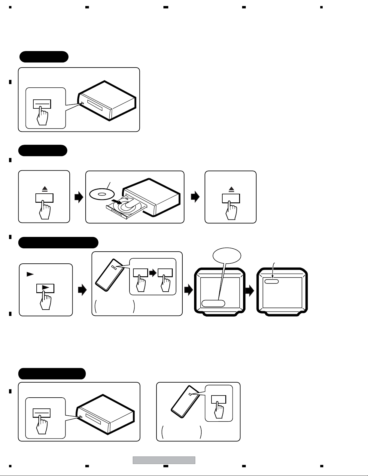
1234
6.2.4 TEST MODE
A
POWER ON
POWER
B
ON
DISC SET
<TRAY OPEN> <TRAY CLOSE>
OPEN/CLOSE
(Player)
C
DVD disc
OPEN/CLOSE
(Player)
TEST MODE: PLAY
CHECK
<PLAY>
Press the play key
( ) of the normal
D
remote control unit.
ESC TEST
DVD, CD
An address is displayed
GGF1381
Test mode
remote control
unit
Notes:
• After going into test mode, if you play back the disc, "DISC-NON" is displayed.
• The video signal and the audio signal are outputted during the test mode.
• The SKIP key and the SCAN key are effective during the test mode.
E
TEST MODE: OFF
POWER
OR
GGF1381
F
82
OFF
1234
Test mode
remote control
unit
XV-EV9
DSC - &&&
ESC
Page 83

5678
6.2.5 MECHANISM ADJUSTMENT
Tangential and Radial Height Coarse Adjustment
1
START
• Remove the 06SD Pickup Assy from the Traverse Mechanism Assy-S.
• Remove the joint and the joint spring of the 06SD Pickup Assy.
A
06SD Pickup Assy
Joint VK1B
Note:
Before removing the flexible cable for the
pickup, soldering of the pickup circuit is
necessary.
For details, see "7.1.13 DISASSEMBLY".
• Pass through the guide shaft to a new 06SD Pickup Assy.
• Attach it to the Traverse Mechanism Assy-S.
Joint spring VK1
Hold spring
Guide Shaft
• Put the joint between the Tangential (or Radial) adjustment screw and the mechanism base
and turn each screw to adjust the height.
(Refer to "6.1 ADJUSTMENT ITEMS AND LOCATION".)
B
06SD Pickup Assy
C
D
• Attach the Traverse Mechanism Assy-S to the 06 LOADER Assy.
• Turn it over and attach the joint and the joint spring.
• Arrange the flexible cables.
(Refer to "7.1.13 DISASSEMBLY".)
XV-EV9
56
Joint
Mechanism base
7
7.5mm
E
F
83
8
Page 84
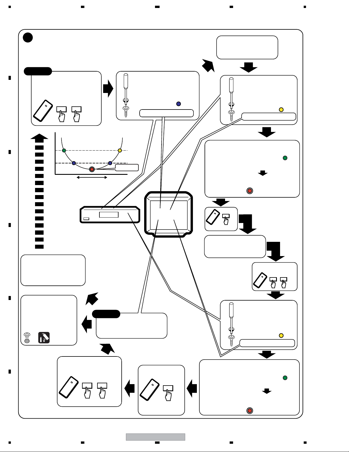
1234
DVD Error Rate Adjustment
A
2
Notes:
• Use disc: GGV1025
• Play the DVD test disc
at inner track
(around #30000)
START
• Play the DVD test disc
at inner track
• Display ERROR RATE
on the monitor
CHP/TIMESC
B
1E-3
ERROR
RATE
5E-4
Anticlock wise Clock wise
C
AA
Rotation of Radial screw
and Tangential screw
Player
Traverse Mechanism
Assy-S
Adjust the radial adjustment
screw so that
ERROR RATE becomes
around "5E-4".
ERROR RATE : "5E-4"
BC
Best point
ERROR RATE: - - - -
Traverse Mechanism
Assy-S
Fasten the radial
adjustment screw so that
A
• Unfasten the radial adjustment screw
by 90 degrees step till ERROR RATE
becomes around "1E-3" again .
• Record the number of rotation (N1).
(memorizing how much the screw was rotated.)
• Fasten the radial adjustment screw
till the number of rotation becomes
harf of N1.
Service mode end
ERROR RATE becomes
around "1E-3".
ERROR RATE : "1E-3"
Best Radial point
ESC
B
C
D
Turn the POWER OFF in
case of NG once, and
perform the adjustment
once again.
If error rate is OK,
locks a root of
tangential and radial
adjustment screws with
the Screw tight.
Screw tight: GYL1001
E
F
NG
CHECK
In this check, the error rate
OK
that is less than "5E-5"is
better.
Disc playback normally.
• The measurement of
block error rate
CHP/TIMESC
Monitor
ESC
Service mode end
• Play the DVD test disc
at outer track
(around #200000)
\ Service mode
CHP/TIMESC
Traverse Mechanism
Assy-S
Fasten the tangential
adjustment screw so that
ERROR RATE becomes
around "1E-3".
ERROR RATE : "1E-3"
• Unfasten the tangential screw
by 90 degrees step till ERROR RATE
becomes around "1E-3" again .
• Record the number of rotation (N1).
• Fasten the tangential adjustment screw
till the number of rotation becomes
harf of N1.
Best tangential point
B
C
84
XV-EV9
1234
Page 85

5678
7. GENERAL INFORMATION
7.1 DIAGNOSIS
7.1.1 TEST MODE
Test Mode Functional Specification
1 Test mode entry
In the power ON state, press the [ESC] (A8-5F) key and [TEST] (A8-5E) key in order of the Test mode remote control
unit.
• OSD displays test mode.
2 LD ON
Enter the test mode.
DVD : Press the [TEST] (A8-5E) and [1] (A8-01) keys in order, and turn on the laser diode (650n).
CD : Press the [TEST] (A8-5E) and [4] (A8-04) keys in order, and turn on the laser diode (780n).
3 Release the Test mode
• Turn off the power.
• Press the [ESC] (A8-5F) key of the remote control unit and reset it.
A
B
C
D
E
56
XV-EV9
F
85
7
8
Page 86

1234
7.1.2 DISPLAY SPECIFICATION OF THE TEST MODE
A
Character in bold : Item name
: Information display
1
5
6
12
B
10
11
1 Address indication
The address being traced is displayed in number.
(as for the DVD, indication of decimal number is possible.)
DVD : ID indication (hexadecimal number, 8 digits)
C
CD : ID indication [∗ ∗ ∗ ∗ ∗ ∗ ∗ ∗]
[∗ ∗ ∗ ∗ ∗ ∗ ∗ ∗]
2 Code indication of remote control unit [R – ∗ ∗ ∗ ∗]
In case of double code, display a 2nd code.
3 Main unit keycode indication [K – ∗ ∗]
5 Tracking status [TRKG – ∗ ∗ ∗]
Tracking on : [ON]
Tracking off : [OFF]
6 Spindle status [SPDL – ∗ ∗ ∗]
D
CLV : [CLV]
Off : [OFF]
7 Mechanism (loading) position value [M – ∗ ∗]
Unknown : [01] or [41]
Open state : [04]
Close state : [08]
During opening : [12]
During closing : [22]
2
3
7
8
9
13
14
15
0 Disc sensing [DSC – ∗ ∗ ∗]
The type of discs loaded is displayed.
[DVD], [CD ]
- Jitter value [J – ∗ ∗ ∗ ∗]
Note: Don't use it.
= Version of the FL controller [FL: ∗ ∗ ∗ ∗]
Note: Don't use it.
~ Region setting of the player [REG: ∗]
Setting value : [1] to [6]
! Destination setting of the FL controller
[MDL: ∗ ∗ ∗ ∗ / ∗ ∗ ∗]
Four characters in the front represent code 01.
Three characters in the back represent the destination code.
J: /J, K: /KU, /KC, /KU/KC, R: /RL/RD, RAM : /RAM,
LB: /LB, WY: /WY
@ Version of the flash ROM [V: ∗ ∗. ∗ ∗]
Flash ROM size [FLASH = ∗ ∗]
8 Slider position [S – ∗ ∗ ∗ ∗]
In Side Switch ON : [01]
E
In Side Switch OFF : [00]
9 Output video system [V – ∗ ∗ ∗ ∗]
NTSC system : [NTSC]
PAL system : [PAL]
Automatic setting : [AUTO]
Scart terminal output [SK – ∗ ∗]
(Display only the WY model which can do the output setting
of scart terminal.)
VIDEO : [00]
S-VIDEO : [01]
F
RGB : [02]
86
1234
XV-EV9
Page 87
5678
7.1.3 FUNCTIONAL SPECIFICATION OF THE SHORTCUT KEY
Only during normal playback, the following shortcut keys can be assigned by pressing a required key after pressing the ESC
key of the remote control unit. To quit, press the ESC key
Command Contents Conditions
Memory clear and region / revision indication CLEAR (∗1) A8-45
Average value measurement of DVD error rate 5 (∗1) A8-05
CD error rate measurement 5 (∗1) A8-05
Scart terminal output : VIDEO
Scart terminal output : S-VIDEO SUBTITLE A3-36
Scart terminal output : RGB ANGLE A3-B5
Progressive OFF
Progressive ON F_SKIP A3-9C
HDMI Resolution : 1920 x 1080i PROGRAM A3-EC
FL indication of ID number STEREO (∗1) A8-4A
ZOOM ON (×4) ZOOM A3-37
Service mode indication (error rate indication, etc.) CHP/TIM (∗1) A8-13
Model information indication CHAP (∗1) A8-40
Title search Input mode IN
Title No. input
Search execution
Region confimation mode
WY, models equipped with Scart terminal
Only for progressive models
Only for HDMI models
Remote Control
Key Name
AUDIO A3-BE
R_SKIP A3-9D
SIDE A (∗1)
Numbers (∗1)
PLAY (∗1)
A.MON (∗1)
Numbers (∗1)
∗1 : Test mode remote control unit
Remote
Control Code
A8-4D
A8-00 to A8-09
A8-17
A8-1E
A8-01 to A8-08
A
B
C
• Service mode indication (ESC + CHP/TIM keys)
ID Address
The error rate is always displayed in exponential notation, e.g., ∗.∗ ∗ e - ∗, for both DVDs and CDs.
EDC/ID/AV 1 error history (ID Address, EDC/ID Error, last eight errors)
• Calculation of the average error rate (ESC + "5" [Test mode remote control unit] keys)
The average of the last eight error rates is calculated and indicated in exponential notation. After the calculation is completed, "OK" or "NG" is
displayed. If "NG" is displayed, the disc tray will open (for both DVDs and CDs)
For DVDs: OK with 5.0e-4 or less, for CDs: OK with 7.6e-3 or less
• Indication of model information (ESC + CHAP keys)
The items from 12 to 15 of the TEST MODE Indications are displayed. However, in the indications, S in the standard test mode is changed to
CHIP VERSION, and M is changed to RF VERSION. For details, see 7.1.4.
D
• Region confirmation mode (ESC + A.MON [Test mode remote control unit] + "1"-"8" [Test mode remote control unit] keys)
After you press the AUDIO key while holding the ESC key pressed and then input the region number, if the number is different from that set in
the unit, an error message is displayed, and the tray opens.
E
56
XV-EV9
F
87
7
8
Page 88
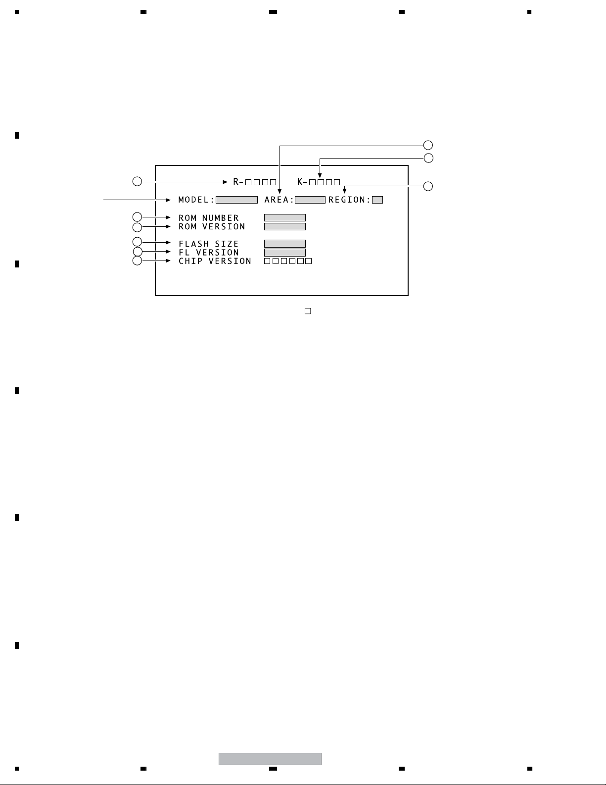
1234
7.1.4 SPECIFICATION OF MODEL INFORMATION DISPLAY
To display model information : Press the ESC key then the CHAP key.
To close the model information display : Press the ESC key.
A
• Display contents
1
10
9
B
C
Don't care.
3
4
5
6
7
1 Destination indication
Display it according to model information set from the FL controller.
2 Region No.
3 Part number
4 ROM version
5 Flash size
6 FL controller version
7 CHIP VERSION
D
2
Character in bold : Item name
: Information display
9 Remote control code
0 Key code of Main unit
E
F
88
1234
XV-EV9
Page 89

5678
7.1.5 FUNCTIONAL SPECIFICATION OF THE SERVICE MODE
• Display during Service Mode
To enter Service Mode, press the CHP/TIM key while holding the ESC key pressed.
To quit, press the ESC key.
Service mode display
1 ID Address
2 Error rate (always displayed), in exponential notation
ERROR RATE : ∗ ∗ ∗ ∗ ∗ ∗ ∗
( ∗ ∗ ∗ ∗ )
Number of error
• Calculation of the average error rate
For DVDs: OK with 5.0e-4 or less, for CDs: OK with 7.6e-3 or less
ex) For DVDs
• Step 1
%%e -&
• Step 2
%%e -4
A
B
%%e -6 : OK
%%e -5 : OK
%%e -4 : Refer to Step 2
%%e -3 : NG
%%e -2 : NG
3.0e -4 : OK
4.0e -4 : OK
5.0e -4 : OK
6.0e -4 : NG
7.0e -4 : NG
3 EDC/ID error history (ID Address, EDC/ID errors, last eight errors)
Note:
∗ Error of AV1 is not supported in this player.
Indication plan contents
1
2
C
3
D
Character in bold : Item name
: Information display
XV-EV9
56
E
F
89
7
8
Page 90

1234
7.1.6 SERVICE TEST MODE
A
1. Conditions during Testmode Check
• VDET does not operate (ignore)
• XPROTECT does not operate(ignore)
• Even if the unit is urgently shut down due to failure in normal mode, it can be POWER ON without waiting for one minute.
2. Way to enter Service Testmode
• Short PIN43(Micro-P STEST) and VE +5, then plug-in AC.
• The following shows some FL difference when testmode is entered, depending on whether testmode is entered after normal power off or
B
emergency shut down.
[After Normal Power Off]
FL display
FL display
FL display
[After Abnormal AMP shutdown]
C
[After Fault in DVD shutdown] [After Fault in EEPROM shutdown]
D
FL display
FL display
FL display
FL display
FL display
FL display
P R T W N G
V O L 0
D V S V C
D V D P R T
V O L 0
D V S V C
W
E L C O M E !
V O L 0
D V S V C
[After Fault in AMP]
FL display
FL display
FL display
FL display
FL display
FL display
* To esc from Testmode, POWER OFF or AC OFF.
* When escape from Testmode, PROTECT related RAM is cleared.
P R T E R R
V O L 0
D V S V C
E E P E R R
V O L 0
D V S V C
Note: EEPROM is an additional item
3. Operation Content
• While in testmode, when basic operation is performed, the following display can be seen when function is changed.
[Functions] [Indications on the FL display]
E
F
90
DVD/CD
TUNER
LINE
TC
D V S V C
X S V C
T
N S V C
L
T C S V C
XV-EV9
1234
Page 91

5678
5
5
8
5
5
5
C
4. Protect Error contents
• The following classifies the error display shown during power on.
P RT W N G
Protect circuit operates
1. Power supply becomes abnormal, could be V+10, V+5, V+3R3, VFDP being shorted or
V+10, V+5, V+3R3 voltage exceeded specification.
2. XPROTECT line from circuit to system microP could be shorted to ground or disconnected somewhere.
P
RT E R R
Protect circuit operates
1. Power supply becomes abnormal, could be V+10, V+5, V+3R3, VFDP being shorted or
V+10, V+5, V+3R3 voltage exceeded specification.
2. XPROTECT line from circuit to system microP could be shorted to ground or disconnected somewhere.
E
EP E R R
1. EEPROM communication line could be disconnected or shorted.
2. EEPROM IC could be spoilt
Note:
- It is advisable to check both XPROTECT and VDET lines to confirm that the set is in normal mode.
A
B
Service Test mode connecting point
MAIN ASSY
C
SIDE B
SIDE B
C
Connecting point
R
R
R
R
R
R5
R5563
R5566
R5567
R5568
R5571
R5570
R5565
R5581
R5596
80
81
R5597
R5598
R5599
R5569
100
R5600
R5572
R5575
R5574
R5573
R5577
R5576
R5584
R5585
C5627
R5627
C5588
R3145
R3144
R3114
R3115
R5556
R5591
3123
R3146
R3121
R5501
R5564
IC5501
R5503
UTEST
50
51
R5513
1
R5618
R5508
R5507
R5504
R5506
STEST
R5537
30
C5514
31
C5603
R5617
C5539
R5616
R5544
R5532
R5530
R5515
14
R5543
R5528
R5526
R5527
2
R5525
C5605
R5610
C5604
1
Q5601
5601
C5622
C5614
R5608
R5621
R5622
R5607
C5612
R5609
Q5603
C5613
Q5604
R5620
D5620
R5623
R5518
R5612
R5613
D
R5
TC
OR
F
E
F
56
XV-EV9
7
8
91
Page 92

1234
1
5
Q
3
R574
R544
D
4
U
7.1.7 METHOD FOR DIAGNOSING DEGRADATION OF THE LDs ON THE PICKUP ASSY
Case when this diagnosis is required :
When playback of any disc, including a test disc (DVD: GGV1025, CD: STD-905), won't play or doesn't play
A
How to diagnose
In the case mentioned above, degradation of the laser diodes (LDs) mounted on the 06SD Pickup Assy is suspected.
Measure the voltage between the two ends of one of the resistors mentioned below.
No playback of a DVD :
Measure the voltage between the both ends of R322 or R325 on the DVDM
Assy. If the voltage is 0.4 V or higher, the 650-nm LD is degraded.
B
No playback of a CD :
Measure the voltage between the both ends of R321 or R326 on the DVDM
Assy. If the voltage is 0.4 V or higher, the 780-nm LD is degraded.
If the measurements show degradation
of an LD, replace the 06SD Pickup
Assy.
PICKUP ASSY
DVDM ASSY
C
CN101
R152
R131
R132
C103
R133
C151
C145
C142
LD_DVD
BOTTOM SIDE
1
R314
R134
R135
R136
C152
C153
1
IC101
C102
44
C133
L308
Q304
C143
C141
3.3V
CN102
C563
C562
R530
R532
C53
24
1
R315
3
R318
R313
C530
C534
Q305
5
4
CN101
R564
R563
C564
R561
R534
R533
R531
C53
BOTTOM SIDE
C371
R373
R565
1
1
8
R535
C561
1
IC531
8
1
IC561
R536
P SIDE
03
P
1
4
C373
C374
R566
Q565
R578
R567
R568
Q563
Q534
R569
79
533
16 9
16
9
UP
1
23
R912
R322
R913
22
Q307
R914
R153
C146
R325
R915
R151
C161
C203
C140
C104
12
C144
LD_CD
L309
3.3V
R154
CN901
R910
R908
R907
R911
IC761
C101
D862
D861
R762
C761
R801
R763
R764
6.5V
GNDM
C132
D801
C801
R321
C131
Q308
C206
R326
D
E
B
SIDE A
F
92
1234
XV-EV9
Page 93

5678
7.1.8 DVD TROUBLE SHOOTING
No. Symptoms Diagnosis Contents Possible Defective Points
1 The power is not turned on. Are wires of output connector (MAIN Assy) and CN901 (DVDM Assy)
An opening screen is not
2
displayed on the monitor
(The FL display lights. The
mechanism does not work.)
disconnected or damaged ?
Check that the following voltage is output :
Q1202-source on the DVDM Assy: 3.3V
Are the signals output from IC201-pin 97 (MDATA) and pin 98 (SCLK)
on the DVDM Assy ? (in the range of 0-3V)
Are the signals input into IC5501-pin 24 (MDATA) and pin 25 (SCLK)
on the DVDM Assy ? (in the range of 0-3V)
Connector / cable
DVDM Assy
DVDM Assy
DVD IC (IC201)
MAIN Assy
UCOM (IC5501)
A
Check that the following voltage are output :
Q1302-collector on the DVDM Assy: 5V
Is a resonator (X201: 27MHz) on the DVDM Assy oscillating ?
•
Is a signal input into IC203-pin26 (PCE#) on the DVDM Assy ?
(Is a signal "H" for 80 mS and then "L" after the power is turned
on ?)
→ Communication with flash ROM.
• Are the signals input into IC202-pin 16 (DWE#), pin 19 (DCS#)
and pin 38 (SDCLK) on the DVDM Assy ?
(Is a signal fluctuating ?)
→ Communication with SDRAM
Is a signal output from IC203-pin 28 (PRD#) on the DVDM Assy? (Is a
signal fluctuating for several hundred mS after the power is turned on
?)
Is a signal input into IC5501-pin 67 (DVD ACK) on the DVDM
Assy ? (Is a signal fluctuating ?)
→ Communication with FL Control IC
Is a signal output from IC5501-pin 78 (XREADY) on the DVDM Assy ?
(Is a signal fluctuating in the range of 0-5V ?)
Are the signals output from IC5501-pin 23 (SDATA) on the DVDM Assy
? (in the range of 0-5V)
DVDM Assy
5V Regulator IC (IC751)
DVDM Assy
Crystal resonator (X201)
DVD IC (IC201)
DVDM Assy
DVD IC (IC201)
Flash ROM (IC203)
SDRAM (IC202)
DVDM Assy
Flash ROM (IC203)
DVDM Assy
DVD IC (IC201)
UCOM (IC5501)
DVDM Assy
UCOM (IC5501)
DVDM Assy
DVD IC (IC201)
MAIN Assy
UCOM (IC5501)
B
C
D
An opening screen is not
3
displayed on the monitor
(The FL display lights. The
mechanism works.)
56
Are the signals of IC204-pin 5 (SDA) and pin 6 (SCL) on the DVDM
Assy fluctuating for one or two seconds after the power is turned?
Check the video signal path between DVD IC (DVDM Assy IC201) and
video-out terminal (see the block diagram)
XV-EV9
7
DVDM Assy
EEPROM (IC204)
DVDM Assy
Video circuit after DVD IC
(IC201)
E
F
93
8
Page 94

1234
No. Symptoms Diagnosis Contents Possible Defective Points
A
A tray cannot be opened.
4
(An opening screen is
displayed on the monitor)
B
Playback impossible
5
(no focusing)
C
Playback impossible
6
(Spindle does not turn)
Does the voltage of CN104-pin 3 and pin 5 on the DVDM Assy change
normally ?
Pin 3 (SW2(TRIN)): Tray is fully closed: "L"
Pin 5 (SW1(TROUT)): Tray is fully opened: "L"
Is the signal input into IC101-pin 11 (TROPEN) on the DVDM Assy?
At open: 3.3V, At close: 0V
Are the signals output from IC101-pin 1 and pin 2 (CN103-pin 1 and
pin 2) on the DVDM Assy ?
Pin 2: Approx. 6V during opening tray approx. 0V during closing tray.
Pin 1: Approx. 0V during opening tray approx. 6V during closing tray.
Are wires of CN104 and CN103 on the DVDM Assy disconnected or
damaged ?
Does the voltage of CN102-pin 1 on the DVDM Assy change to 0V by
pressing the Inside switch.
Are the signals output from IC101-pin 3 (FOCS_DRV) and pin 4
(FOCS_RTN) on the DVDM Assy ?
Does 650-nm LD emit light ?
Does a pickup lens move up / down ?
Does an actuator spring bend ?
Are plastic parts damaged ? Or is a shaft detached ?
Is the turntable detached or tilted ?
Is flexible cable of CN101 on the DVDM Assy disconnected or
damaged ?
Is signal output from IC201-pin 42 (FOSO) on the DVDM Assy ?
(Device control of about 1.4 V is output usually. It is fluctuated by about
± 250 mV with focus up / down.)
Are the signals output from IC101-pin 30 (W), pin 33 (V) and pin 35 (U)
on the DVDM Assy ?
Is pin 26 (STBY) fixed LOW ? (pin 26 is High at playback: 3V)
Is there any part detached from the spindle motor ?
Or Is there any foreign object lodged in it ?
Are wires of CN102 on the DVDM Assy disconnected or damaged ? Flexible cable / connector
LOAB Assy
Tray SW (S101)
DVDM Assy
DVD IC (IC201)
DVDM Assy
FTS Driver IC (IC101)
Connector / cable
Inside switch
DVDM Assy
FTS Driver IC (IC101)
Pickup
Mechanism section (motor)
Flexible cable / connector
DVDM Assy
DVD IC (IC201)
DVDM Assy
FTS Driver IC (IC101)
Mechanism section
(Spindle motor)
Is signal output from IC201-pin 37 (DMSO) on the DVDM Assy ?
Does 650-nm LD deteriorate ?
If the voltage at each both ends of R322 and R325 on the DVDM Assy
D
Playback impossible
7
(Playback stops)
Picture disturbance during
8
playback
(block noise, freeze, other)
E
No sound
9
(Picture is normal)
is 0.4 V or more, the 650-nm LD is definitely deteriorated.
Does 780-nm LD deteriorate ?
If the voltage at each both ends of R321 and R326 on the DVDM Assy
is 0.4 V or more, the 780-nm LD is definitely deteriorated.
Is there abnormality in FG waveform ? (IC201-pin 50)
Are there scratches or dirt on the disc ? Disc
Are there scratches or dirt on the disc ?
Is there a problem with the format of the disc ?
Check the video signals.
Composite video signal (IC401-pin 25)
S video signal (IC401-pin 21, pin 26)
RGB video signal (IC401-pin 16, pin 18, pin 20)
Check the waveform (ALCK : IC201-pin 212), (ALRCK : IC201-pin
209), (ABCK : IC201-pin 210), (ASDATA0 : IC201-pin 197).
DVDM Assy
DVD IC (IC201)
650-nm LD deteriorated.
(When playback of a DVD is
impossible)
780-nm LD deteriorated.
(When playback of a CD is
impossible)
DVDM Assy
FG output : FTS Driver IC (IC101)
Disc
DVDM Assy
DVD IC (IC201)
Video IC (IC401, IC451)
DVDM Assy
DVD IC (IC201)
F
94
1234
XV-EV9
Page 95

5678
Symptoms that may occur when any of the following ICs is in failure
IC Symptoms
EEP ROM
(DVDM Assy : IC204)
User's data cannot be stored in memory.
A
Flash ROM
(DVDM Assy : IC203)
DVD IC
(DVDM Assy : IC201)
64M SDRAM
(DVDM Assy : IC202)
The power cannot be turned on.
Downloading of the firmware cannot be performed. The ID number is lost.
Any kind of symptoms (no power, a failure in any of the servo, video and audio systems, etc.) may be
generated, because the DVD processing is performed by a single chip.
No power.
Block noise is generated during playback.
B
C
D
E
F
56
XV-EV9
95
7
8
Page 96

1234
7.1.9 ID NUMBER AND ID DATA SETTING
Caution:
For the DVD players compatible with DVD-RW, for playback of a DVD-RW disc (CPRM) and for the DVD players possessing
A
HDMI output, for HDCP process, it is necessary that an individual ID number and ID data are set for each player. If the ID
number and ID data be not properly set in the manner described below, future operations cannot be guaranteed. The ID
number is written on the yellow label at the rear panel of the player.
If there is no yellow label, before downloading FLASH ROM, take note of the ID number set following the procedures
outlined in "ID Number Confirmation Mode" on the next page.
Note: Enter ID numbers while the unit is in Stop mode so that the values set will be immediately written to the flash ROM.
Setting an ID number or ID data is required in the
following case:
If "No NUM" or "NO DATA" is displayed on the FL display
for a few seconds immediately after the power to the player
is turned on or during Stop mode.
B
JIGS AND MEASURING INSTRUMENTS
Service Remote Control Unit
[GGF1381]
C
DVD Data Disc
[GGV1269]
ID Number Input Mode
To enter ID Number Input Mode, with no ID number set, such as
1
in a case of immediately after upgrading the firmware, press the
ESC key then the STEREO key.
Note: If a previous ID number and ID data, such as a factory-
preset ID number and ID data, are maintained, the unit
enters ID Number Confirmation Mode when the above keys
are pressed. However, if only an ID number is maintained,
the unit enters ID Data Input Mode.
Enter a 9-digit ID number. The ID number is also displayed on
2
D
the FL display.
By pressing the CLEAR key without having input a number, you
3
can exit this mode. Each press of this key after a number has
been input deletes one digit.
After entering all 9 digits, if you press the SEARCH key, the
5
unit unconditionally sets the input number as the ID number.
Then the unit automatically enters Player's Data Input Mode.
(The SEARCH key is not accepted until after all 9 digits have
been entered.)
[Player's ID Number Setting]
ID Number ?
0 0 0 0 0 0 0 0 1
4
<PLAY> Compare Mode
<SEARCH> Enter
5
Input ID Number !
This display appears when the PLAY key is pressed in Step 4.
6
Enter a 9-digit number to compare. The number is also
displayed on the FL display.
By pressing the CLEAR key without having input a number, the
7
unit returns to Step 2 without doing anything else. Each press
of this key after a number has been input deletes one digit.
[Player's ID Number Setting]
ID Number ?
0 0 0 0 0 0 0 0 1
Compare
∗ ∗ ∗ ∗ ∗ ∗ ∗ ∗ ∗
6
Input ID Number !
[Player's ID Number Setting]
ID Number ?
- - - - - - - - -
2
3
<CLEAR> Exit
E
Input ID Number !
After entering all 9 digits, if you press the PLAY key, the unit
4
enters Compare mode. Enter the same ID number again. Only
if your two input numbers match, the ID number is set. Compare
mode helps eliminate mistyping of the ID number.
Note: If you press the PLAY button before inputting a 9-digit ID
number, the unit returns to Step 2 without doing anything
F
else.
96
1234
XV-EV9
After entering all 9 digits, if you press the PLAY key, the unit
8
compares the numbers input in Steps 2 and 6, and only if the
numbers match, that number is set as the ID. Then the unit
automatically enters ID DATA Input Mode. If the numbers do not
match, the disc tray is opened, and the unit exits ID Number
Input Mode.
Note: If you press the PLAY button before inputting a 9-digit ID
number, the unit returns to Step 6 without doing anything
else.
[Player's ID Number Setting]
ID Number ?
0 0 0 0 0 0 0 0 1
Compare
0 0 0 0 0 0 0 0 1
<PLAY> Enter
8
Input ID Number !
Page 97
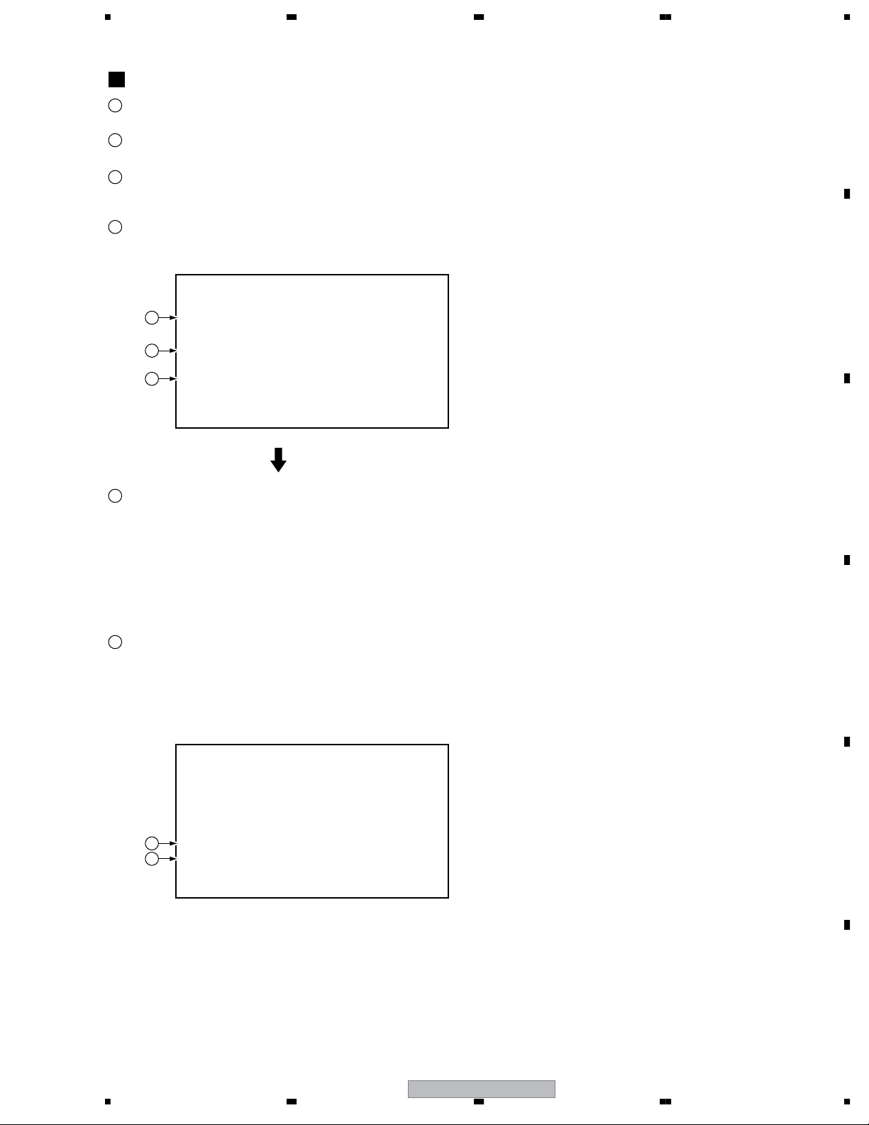
5678
ID Number Confirmation Mode
To enter ID Number Confirmation Mode after the ID number and
1
the ID data are set, press the ESC key then the STEREO key.
The ID number already set is displayed.
2
(It is also displayed on the FL display.)
Enter a 9-digit number for comparison. This is not required
3
when you only wish to check the ID number visually.
(The number is also displayed on the FL display.)
By pressing the CLEAR key without having input a number, you
4
can exit this mode. Each press of this key after a number has
been input deletes one digit.
• Indication of an ID number already set
An ID number already set is displayed in the following cases:
1) When the ESC key then the CLEAR key are pressed, user
settings are cleared, then the ID number set is displayed on
the screen. In this case, the ID number is not displayed on the
FL display.
2) When the unit enters ID Number Confirmation Mode by your
pressing the ESC key then the STEREO key, the ID number
set is displayed. In this case, the ID number is also displayed
on the FL display.
If you only need to confirm the ID number, you can exit
this mode by pressing the CLEAR key or turning off the power.
A
[Player's ID Number Setting]
ID Number ?
0 0 0 0 0 0 0 0 1
2
Compare
∗ ∗ ∗ ∗ ∗ ∗ ∗ ∗ ∗
3
<CLEAR> Exit
4
Input ID Number !
After entering all 9 digits, if you press the PLAY key, the unit
5
compares the number entered in Step 2 with the ID number
set, and only if the numbers match, the unit automatically exits
ID Number Confirmation Mode. If an ID data has not been
entered, the unit enters ID DATA Input Mode. If the numbers do
not match, the disc tray is opened, and the unit exits ID Number
Confirmation Mode.
Note: If you press the PLAY button before inputting a 9-digit ID
number, the unit returns to Step 4 without doing anything
else.
After entering all 9 digits, if you press the STOP key, the unit
6
compares the number entered in Step 3 with the ID number
set, and only if the numbers match, the unit automatically
deletes the ID number and exits this mode. If the numbers do
not match, the disc tray is opened, and the unit exits this mode.
(The STOP key is only accepted after the correct 9 digits have
been entered.)
• Indication when no ID number is set
If no ID number is set, the message "No ID NUM" flashes on FL
display for a few seconds after the power is turned on or during
Stop mode.
B
C
D
[Player's ID Number Setting]
ID Number ?
0 0 0 0 0 0 0 0 1
Compare
0 0 0 0 0 0 0 0 1
5
<PLAY> Enter
<STOP> Memory Clear
6
Input ID Number !
56
XV-EV9
E
F
97
7
8
Page 98

1234
ID DATA Input Mode
A
To enter ID DATA Input Mode, with the ID number set, press the
1
ESC key then the STEREO key.
When the STEREO key is pressed, the unit enters ID DATA
2
Input Mode.
When writing of the data read from the disc to flash ROM is
5
completed, "Rom Write OK!" is displayed. After seeing this
message, you can exit this mode by pressing the CLEAR key.
Note: Whether or not the data have been written to flash ROM can
be confirmed by watching for the message "Rom Write OK!"
being displayed after the disc is read.
[Player's ID Number Setting]
ID Number ?
[ 0 0 0 0 0 0 0 0 1 ]
Compare
B
> ∗ ∗ ∗ ∗ ∗ ∗ ∗ ∗ ∗
<CLEAR> Exit
<STEREO> ID Data Setting Mode
2
Input ID Number !
If the DVD DATA DISC is loaded in this mode, the unit
3
automatically starts reading the data.
(If the DVD DATA DISC has already been loaded, the unit does
not start reading the data. In this case, open then close the
C
tray.)
To exit this mode, press the CLEAR key. While data are being
4
read from the DVD DATA DISC, you cannot exit this mode.
[Player's Data Input Mode]
[Player's Data Input Mode]
5
Rom Write OK!
<CLEAR> Exit
If the data cannot be read from the disc, "Disc Error!" is
6
displayed on the screen, and the disc is ejected.
[Player's Data Input Mode]
6
Disc Error!
<CLEAR> Exit
D
E
F
<CLEAR> Exit
4
Insert The ID Data Disc !
• Indication when the data have not been set
If no ID data are set after the ID number is changed, the message
"NO DATA" flashes on the screen and FL display for a few seconds
after the power is turned on or during Stop mode.
98
XV-EV9
1234
Page 99

5678
7.1.10 DISASSEMBLY
Note 1: Do NOT look directly into the pickup lens. The laser beam may cause eye injury.
Note 2: Even if the unit shown in the photos and illustrations in this manual may differ from your product, the procedures
described here are common.
Note 3: For performing the diagnosis shown below, the following jigs for service is required:
• Cable for service (GGD1425)
Diagnosis of PCB's
1
Bonnet and Tray panel
A
Remove 4 screws from Bonnet L and R (BPZ30P080FNI).
1
Remove 2 screws from Bonnet L and R (BBZ30P080FNI).
2
Remove the Bonnet by removing the 6 screws
3
(BBZ30P080FNI).
3
Rear View
Press the STANDBY/ON button to turn on the power.
4
Press the OPEN/CLOSE button to open the Tray.
5
Remove the Tray Cap.
6
Set the Test Disc.
7
Press the OPEN/CLOSE button to close the Tray.
8
(Test Disc is clamped.)
Press the STANDBY/ON button to turn off the power.
9
Pull out the Power cord.
10
How to open the Tray when the power cannot be on
Insert a Tweezer(as shown in the photo) into the Slit located at
the bottom of the unit and slide the projection of the Drive Cam in
1
2
the Loader ASSY in the direction of the arrow, as indicated in the
photo.
If the Tray pops out a little, fully pull it out by hand.
Tweezer
Slit
B
C
D
6
Tray Cap
5
4 9
5
8
7
Test Disc
8
56
XV-EV9
Bottom View
E
F
99
7
8
Page 100

1234
2
Disassembly of Front Panel ASSY and MAIN ASSY diagnosis
A
Remove 2 screws at bottom side of the unit.
1
Remove 4 screws(BPZ30P080FNI) at the Rear Panel of the unit.
5
Remove 2 screws(BBZ30P080FNI) on the MAIN ASSY .
6
1
B
Bottom View
C
D
Remove the grounding screw.
2
Unhook the Cable Hook .
3
Released the hook at the right and left side of the Front
4
Panel ASSY.
5
Rear View
In the event that Power Amplifier ASSY was removed and
7
repaired(MAIN ASSY had been removed)
If you want to power on the set with MAIN ASSY removed
from the Rear Panel, make sure both the EVOL and RCA
grounds are connected to the Rear Panel as shown in
the attached photo.
MAIN ASSY
6
RCA Ground
SPEAKER
JACK GND
E
3
Rear View
MAIN ASSY
VIDEO
JACK GND
2
4
Front Panel ASSY
F
100
1234
XV-EV9
 Loading...