

Page 1
PIONEER CORPORATION 4-1, Meguro 1-chome, Meguro-ku, Tokyo 153-8654, Japan
PIONEER ELECTRONICS (USA) INC. P.O. Box 1760, Long Beach, CA 90801-1760, U.S.A.
PIONEER EUROPE NV Haven 1087, Keetberglaan 1, 9120 Melsele, Belgium
PIONEER ELECTRONICS ASIACENTRE PTE. LTD. 253 Alexandra Road, #04-01, Singapore 159936
PIONEER CORPORATION 2004
12345
FM/AM/ST.
DVD/CD TUNER TV/L1/L2
XV-HTD540
CD MODE TIMER
DISC SKIP EXCHANGE
OPEN/CLOSE
VOLUME
DOWN
UP
PHONES
DIRECT PLAY
12345
STANDBY/ON
DISC
DVD/CD RECEIVER
XV-HTD540
XV-DV8
THIS MANUAL IS APPLICABLE TO THE FOLLOWING MODEL(S) AND TYPE(S).
Model Type Power Requirement Region No. Remarks
XV-HTD540 KUCXJ AC120V 1
XV-DV8 DDXJ/RA AC120-127/220-230/240V 1
XV-DV8 DDXJ/RB AC120-127/220-230/240V 2
XV-DV8 DLXJ/NC AC120-127/220-230/240V 3
XV-DV8 DPWXJ AC120-127/220-230/240V 4
ORDER NO.
RRV2908
For details, refer to "Important symbols for good services" .
T-ZZR APR 2004 printed in Japan
Page 2
1234
SAFETY INFORMATION
A
This service manual is intended for qualified service technicians; it is not meant for the casual
do-it-yourselfer. Qualified technicians have the necessary test equipment and tools, and have been
trained to properly and safely repair complex products such as those covered by this manual.
Improperly performed repairs can adversely affect the safety and reliability of the product and may
void the warranty. If you are not qualified to perform the repair of this product properly and safely, you
should not risk trying to do so and refer the repair to a qualified service technician.
WARNING
This product contains lead in solder and certain electrical parts contain chemicals which are known to the state of California to
B
cause cancer, birth defects or other reproductive harm.
Health & Safety Code Section 25249.6 – Proposition 65
NOTICE
(FOR CANADIAN MODEL ONLY)
Fuse symbols (fast operating fuse) and/or (slow operating fuse) on PCB indicate that replacement
parts must be of identical designation.
REMARQUE
(POUR MODÈLE CANADIEN SEULEMENT)
Les symboles de fusible (fusible de type rapide) et/ou (fusible de type lent) sur CCI indiquent que
C
les pièces de remplacement doivent avoir la même désignation.
(FOR USA MODEL ONLY)
1. SAFETY PRECAUTIONS
The following check should be performed for the
continued protection of the customer and service
technician.
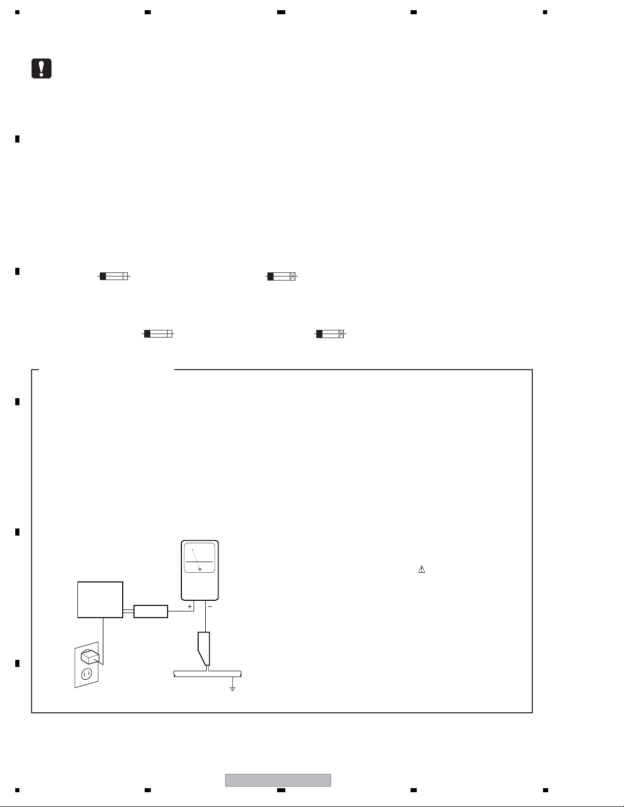
LEAKAGE CURRENT CHECK
Measure leakage current to a known earth ground
(water pipe, conduit, etc.) by connecting a leakage
current tester such as Simpson Model 229-2 or
D
equivalent between the earth ground and all exposed
metal parts of the appliance (input/output terminals,
screwheads, metal overlays, control shaft, etc.). Plug
the AC line cord of the appliance directly into a 120V
AC 60 Hz outlet and turn the AC power switch on. Any
current measured must not exceed 0.5 mA.
Leakage
current
E
Device
under
test
Also test with
plug reversed
(Using AC adapter
plug as required)
Test all
exposed metal
surfaces
AC Leakage Test
tester
Reading should
not be above
0.5 mA
Earth
ground
ANY MEASUREMENTS NOT WITHIN THE
LIMITS OUTLINED ABOVE ARE INDICATIVE
OF A POTENTIAL SHOCK HAZARD AND
MUST BE CORRECTED BEFORE RETURNING THE APPLIANCE TO THE CUSTOMER.
2. PRODUCT SAFETY NOTICE
Many electrical and mechanical parts in the appliance
have special safety related characteristics. These are
often not evident from visual inspection nor the
protection afforded by them necessarily can be obtained
by using replacement components rated for voltage,
wattage, etc. Replacement parts which have these
special safety characteristics are identified in this
Service Manual.
Electrical components having such features are
identified by marking with a
on the parts list in this Service Manual.
The use of a substitute replacement component which
does not have the same safety characteristics as the
PIONEER recommended replacement one, shown in the
parts list in this Service Manual, may create shock, fire,
or other hazards.
Product Safety is continuously under review and new
instructions are issued from time to time. For the latest
information, always consult the current PIONEER
Service Manual. A subscription to, or additional copies
of, PIONEER Service Manual may be obtained at a
nominal charge from PIONEER.
on the schematics and
F
2
1234
XV-HTD540
Page 3
5678
[ Important symbols for good services ]
In this manual, the symbols shown-below indicate that adjustments, settings or cleaning should be made securely.
When you find the procedures bearing any of the symbols, be sure to fulfill them:
1. Product safety
You should conform to the regulations governing the product (safety, radio and noise, and other regulations), and
should keep the safety during servicing by following the safety instructions described in this manual.
2. Adjustments
To keep the original performances of the product, optimum adjustments or specification confirmation is indispensable.
In accordance with the procedures or instructions described in this manual, adjustments should be performed.
3. Cleaning
For optical pickups, tape-deck heads, lenses and mirrors used in projection monitors, and other parts requiring cleaning,
proper cleaning should be performed to restore their performances.
4. Shipping mode and shipping screws
To protect the product from damages or failures that may be caused during transit, the shipping mode should be set or
the shipping screws should be installed before shipping out in accordance with this manual, if necessary.
A
B
5. Lubricants, glues, and replacement parts
Appropriately applying grease or glue can maintain the product performances. But improper lubrication or applying
glue may lead to failures or troubles in the product. By following the instructions in this manual, be sure to apply the
prescribed grease or glue to proper portions by the appropriate amount.For replacement parts or tools, the prescribed
ones should be used.
CONTENTS
SAFETY INFORMATION......................................................................................................................................2
1. SPECIFICATIONS .............................................................................................................................................5
2. EXPLODED VIEWS AND PARTS LIST.............................................................................................................6
2.1 PACKING....................................................................................................................................................6
2.2 EXTERIOR SECTION ................................................................................................................................8
2.3 FRONT PANEL SECTION ........................................................................................................................10
2.4 AMP POWER MODULE ...........................................................................................................................12
2.5 TRAVERSE MECHA ASSY 03-S..............................................................................................................13
2.6 TABLE MECHANISM SECTION ...............................................................................................................14
3. BLOCK DIAGRAM AND SCHEMATIC DIAGRAM ..........................................................................................16
3.1 BLOCK DIAGRAM DVD SECTION...........................................................................................................16
3.2 BLOCK DIAGRAM MAIN SECTION.........................................................................................................18
3.3 OVERALL WIRING DIAGRAM .................................................................................................................20
3.4 DVDM ASSY (1/4) ....................................................................................................................................22
3.5 DVDM ASSY (2/4) ....................................................................................................................................24
3.6 DVDM ASSY (3/4) ....................................................................................................................................26
3.7 DVDM ASSY (4/4) HTD540 Only..............................................................................................................28
3.8 DSP ASSY (1/2) .......................................................................................................................................30
3.9 DSP ASSY (2/2) .......................................................................................................................................32
3.10 6CH AMP ASSY .....................................................................................................................................34
3.11 AF ASSY (1/4) and DVD TRADE ASSY(HTD540 Only).........................................................................36
3.12 AF ASSY (2/4) ........................................................................................................................................38
3.13 AF(3/4) ASSY .........................................................................................................................................40
3.14 AF(4/4), DIODE L and DIODE S ASSYS................................................................................................42
3.15 TRSB, SSRB, LOMB and SSIB ASSYS .................................................................................................44
3.16 PRIMARY, AMP TRADE, DSP TRADE and VIDEO JACK ASSYS.........................................................46
C
D
E
F
56
XV-HTD540
3
7
8
Page 4

1234
3.17 DISPLAY, FUNCTION KEY, DISC KEY, HP MIC and JOG ASSYS ....................................................... 48
3.18 DVDM WAVEFORMS............................................................................................................................. 50
4. PCB CONNECTION DIAGRAM ..................................................................................................................... 53
4.1 TRSB, SSRB and LOMB ASSYS............................................................................................................. 52
A
4.2 SSIB and DVD TRADE ASSYS................................................................................................................ 53
4.3 DVDM ASSY (HTD540 Only)................................................................................................................... 54
4.4 DVDM ASSY (DV8 / Other) ...................................................................................................................... 56
4.5 AF ASSY.................................................................................................................................................. 58
4.6 6CH AMP ASSY ...................................................................................................................................... 62
4.7 DSP, DSP TRADE and AMP TRADE ASSYS..........................................................................................64
4.8 VIDEO JACK and PRIMARY ASSYS....................................................................................................... 66
4.9 DISPLAY, JOG, DISC KEY, HP MIC, DIODE L, R and FUNC KEY ASSYS ............................................ 68
5. PCB PARTS LIST ........................................................................................................................................... 72
6. ADJUSTMENT ............................................................................................................................................... 81
6.1 ADJUSTMENT ITEMS AND LOCATION ................................................................................................. 82
B
6.2 JIGS AND MEASURING INSTRUMENTS............................................................................................... 82
6.3 NECESSARY ADJUSTMENT POINTS ................................................................................................... 83
6.4 TEST MODE ............................................................................................................................................ 84
6.5 MECHANISM ADJUSTMENT.................................................................................................................. 85
7. GENERAL INFORMATION ............................................................................................................................. 87
7.1 DIAGNOSIS ............................................................................................................................................. 87
7.1.1 TEST MODE ...................................................................................................................................... 87
7.1.2 DISPLAY SPECIFICATION OF THE TEST MODE............................................................................ 89
7.1.3 FUNCTIONAL SPECIFICAION OF THE SHORTCUT KEY .............................................................. 90
7.1.4 SPECIFICAION OF MODEL INFORMATION DISPLAY .................................................................... 91
7.1.5 FUNCTIONAL SPECIFICAION OF THE SERVICE MODE............................................................... 92
7.1.6 MECHANICAL ERROR HISTORY..................................................................................................... 93
C
7.1.7 ID NUMBER AND ID DATA SETTING............................................................................................... 98
7.1.8 TROUBLE SHOOTING.................................................................................................................... 101
7.1.9 DSP TROUBLE SHOOTNG ............................................................................................................ 106
7.1.10 POWER ON SEQUENCE.............................................................................................................. 108
7.1.11 WAVEFORM POINTS LOCATION................................................................................................. 109
7.1.12 PROTECTION CIRCUIT................................................................................................................ 112
7.1.13 DISASSEMBLY .............................................................................................................................. 117
7.2 PARTS.................................................................................................................................................... 133
7.2.1 IC ..................................................................................................................................................... 133
7.2.2 DISPLAY.......................................................................................................................................... 139
7.2.3 DISC / CONTENT FORMAT PLAYBACK COMPATIBILITY............................................................. 140
7.2.4 CLEANING ...................................................................................................................................... 141
8. PANEL FACILITIES ...................................................................................................................................... 142
D
E
F
4
1234
XV-HTD540
Page 5
5678
1. SPECIFICATIONS
Specifications
Amplifier Section
Continuous Power Output (RMS):
Front,center,surround .....100 W per channel
Ω
(1 kHz,10 %T.H.D.,6
)
Subwoofer ....100 W (100 Hz,10 %T.H.D.,6
Disc section
Digital audio
characteristics ........ DVD fs:96 kHz,24-bit
Type ......DVD system,video CD system and
compact disc digital audio system
Frequency response ........... 4 Hz to 44 kHz
Wow and Flutter ....... Limit of measurement
±
0.001 %W.PEAK)or less (EIAJ)
(
Tuner Section
FM tuner section
Frequency range............. 87.5 to 108 MHz
Ω
Antenna.................. 75
AM tuner section
Frequency range
With 9 kHz step......... 531 kHz to 1,602 kHz
With 10 kHz step........ 530 kHz to 1,700 kHz
(Not applicable to the Saudi Arabian model)
Antenna..................... Loop antenna
Note:
• Specifications and design subject to possible modification without notice, due improvements.
,unbalanced
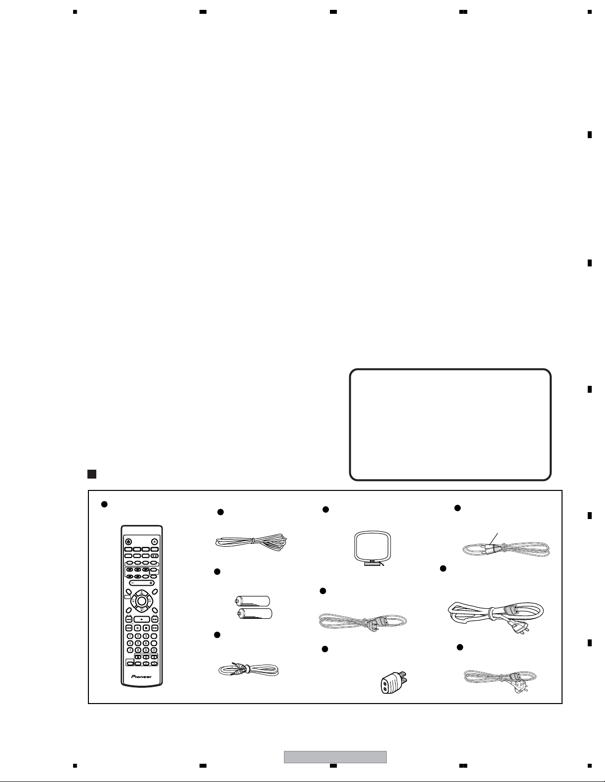
Accessories
Miscellaneous
A
Power Supply Section (XV-HTD540)
............... AC 120 V,60 Hz
Power requirements. . . . . . AC 120-127/220-230/
(XV-DV8) 240 V (switchable), 50/60 Hz
Ω
)
Power consumption
....................... 180 W
Power consumption in standby
...................... 0.5 W
Dimensions ... 420 (W)x 126 (H)x 445 (D)mm/
16-9/16 (W)x 4-15/16 (H)x 17-5/8 (D)in.
Weight .................... 9.8 kg/21 lb 10 oz
B
Accessories (DVD/CD receiver)
Remote control Unit .............................................................. 1
AA/R6P dry cell batteries ...................................................... 2
AM loop antenna ................................................................... 1
FM antenna ........................................................................... 1
Video cord (yellow plugs) ..................................................... 1
Mini jack cable ...................................................................... 1
Power cord ............................................................................ 1
Power plug adapter (Central and South American models,
PX model) . . . . . . . . . . . . . . . . . . . . . . . . . . . 1
These operating instructions . . . . . . . . . . . . . . . . . . . . . . . . .. . .1
C
Warranty Card (Australian and PX model) . . . . . . . . . . . . . .. . .1
* Manufactured under license from
Dolby Laboratories. “Dolby”, “Pro
Logic”, and the double-D symbol are
trademarks of Dolby Laboratories.
** “DTS” and “DTS Digital Surround”
are registered trademarks of Digital
D
Theater Systems, Inc.
Remote Control Unit x 1
(XXD3080)
STANDBY/ON
OPEN/CLOSE
L1/L2FM/AM
DVD/CD
TV LINE
TUNER
BASS MODE
DIALOGUE VIR. SB
FRONT
SURROUND ADVANCED
SOUND
SURROUND
MODE
SUBTITLE
ANGLE ZOOM
AUDIO
ROOM
DISC 1 DISC 2
DISC 3
SETUP
CD MODE
DISC 4 DISC 5
DISC SKIP
MUTE
VOLUME
SYSTEM SETUP
TOP MENU
DVD MENU
HOME
MENU
ENTER
QUIET/
MIDNIGHT
RETURN
FOLDER
FOLDER
PROGRAM
REPEAT RANDOM
CLEAR
TEST TONE CH LEVEL
TIMER
ENTER
DISPLAYSR +
DIMMER
TV CONTROL
CHANNELINPUT VOLUME
SHIFT
SURROUND
5.1ch DVD SYSTEM
FM Antenna x 1
(ADH7030)
AA/R6P Dry Cell
x
Batteries
2
Mini Jack Cable
(ADE7095)
AM Loop Antenna x 1
(ATB7013)
Power Cord
(XV-HTD540 : ADG7021)
Power Plug Adapter
(XV-DV8/DDXJ/RA Only
XKM3001)
XV-HTD540
56
Video Cord x 1
(XDE3046)
Yellow (L=1.5m)
Power Cord
(XV-DV8/DLXJ/NC : ADG1154)
x
1
(XV-DV8/DDXJ/RA : ADG1154)
(XV-DV8/DPWXJ : ADG7099)
x
1
E
Power Cord x 1
(XV-DV8/DDXJ/RB : ADG1158)
F
5
7
8
Page 6
1234
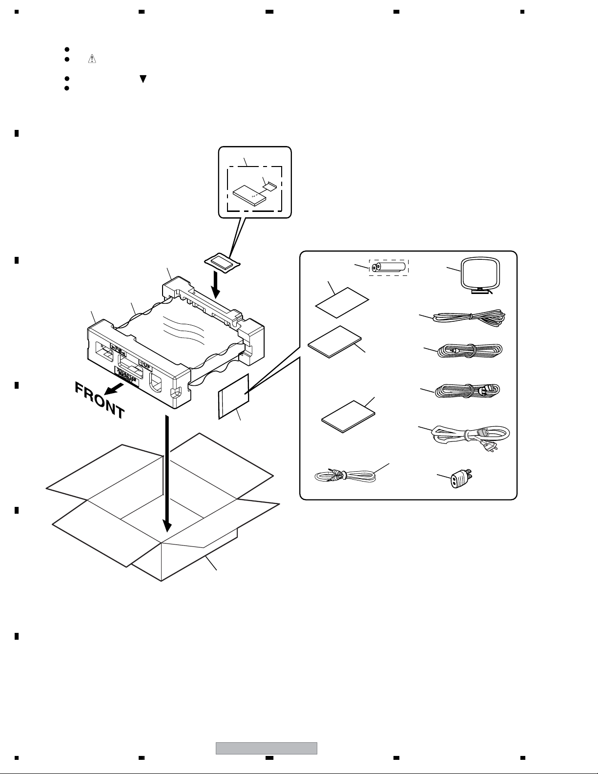
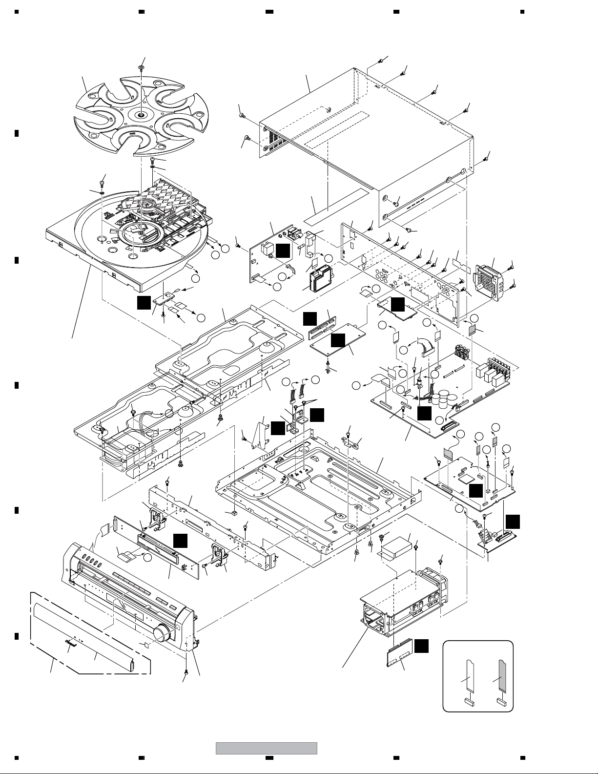
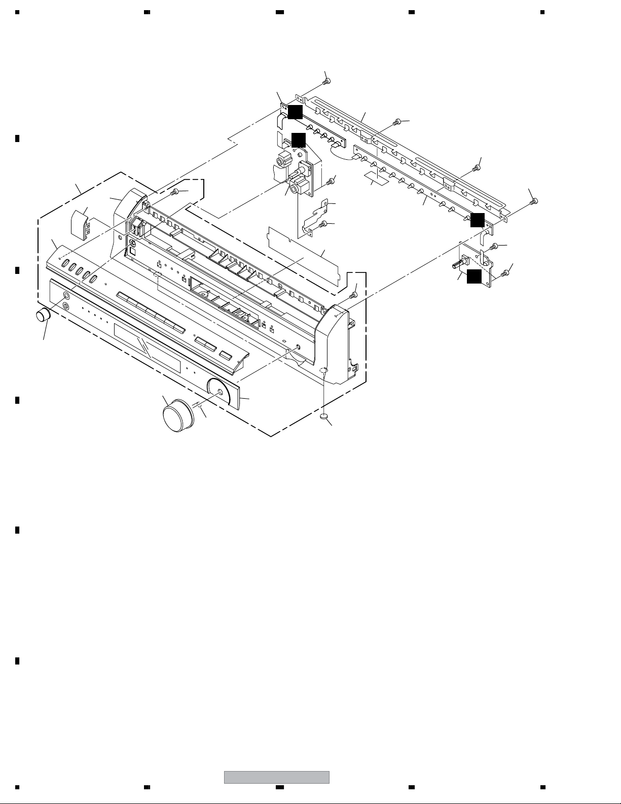
2. EXPLODED VIEWS AND PARTS LIST
NOTES:
A
Parts marked by "NSP" are generally unavailable because they are not in our Master Spare Parts List.
The mark found on some component parts indicates the importance of the safety factor of the part.
Therefore, when replacing, be sure to use parts of identical designation.
Screws adjacent to mark on product are used for disassembly.
For the applying amount of lubricants or glue, follow the instructions in this manual.
(In the case of no amount instructions, apply as you think it appropriate.)
2.1 PACKING
B
C
13
12
14
3
4
5
10
7
6
8
9
11
D
E
15
2
1
1
17
16
F
6
1234
XV-HTD540
Page 7
>
>
5678
PACKING parts List
No. Description Part No.
Mark
1Power Cord See Contrast table(2)
2 Video Cord (L = 1.5m) XDE3046
3 Remote Control Unit XXD3080
4 Battery Cover AZN7933
NSP 5 Dry Cell Battery (R6P, AA) VEM1031
No. Description Part No.
Mark
NSP 10 Warranty Card See Contrast table(2)
NSP 11 Polyethylene Bag Z21-038
(0.03 x 230 x 340)
12 Packing Sheet AHG7010
13 Front Pad (PS) XHA3143
A
6 FM Antenna Assy ADH7030
7 AM Loop Antenna Assy ATB7013
8 Operating Instructions See Contrast table(2)
9 Operating Instructions See Contrast table(2)
14 Rear Pad (PS) XHA3144
15 Packing Case (PAP) See Contrast table(2)
16 Power Plug adapter See Contrast table(2)
17 Mini Jack Cable(4P) ADE7095
(2) CONTRAST TABLE
XV-DV8/DDXJ/RA, DDXJ/RB, DLXJ/NC, DPWXJ and XV-HTD540/KUCXJ are constructed the same except for the
following :
Part No.
Mark No. Symbol and Description
1AC Power Cord ADG7021 ADG1154 ADG1158 ADG1154 ADG7099
8 Operating Instructions XRB3032
9 Operating Instructions XRC3123
NSP 10 Warranty Card ARY7045 ARY7025 Not used Not used ARY7047
15 Packing Case XHD3418 XHD3452 XHD3420 XHD3424 XHD3426
16 Power Plug Adapter Not used XKM3001 Not used Not used Not used
XV-HTD540
/KUCXJ
(English)
(French)
XV-DV8
/DDXJ/RA
XRB3033
(English)
Not used XRC3126
XV-DV8
/DDXJ/RB
XRB3040
(English)
(Arabic)
XV-DV8
/DLXJ/NC
XRB3033
(English)
XRC3125
(Chinese)
XV-DV8
/DPWXJ
XRB3033
(English)
Not used
B
C
D
E
F
56
XV-HTD540
7
7
8
Page 8
1234
2.2 EXTERIOR SECTION
A
B
C
Refer to
"2.6 TABLE MECHANISM SECTION".
D
35
33
51
49
14
51
48
G
50
50
42
53
28
50
36
7
50
E
C
24
K
15
18
F
M
13
22
54
A
10
N
B
2
27
L
E
J
52
50
20
50
23
K
29
4
5
F
53
11
16
53
50
50
H
O
M
G
I
K
50
3
21
49
33
B
from
Traverse
6
46
F
50
from
Traverse
50
G
D
50
50
53
37
50
D
50
50
50
43
50
53
50
53
A
L
N
I
50
30
50
50
50
H
19
E
B
D
C
50
38
50
17
J
E
44
40
41
39
F
8
1234
25
31
L
8
50
38
50
32
34
28
55
52
52
M
Refer to
50
"2.3 FRONT PANEL SECTION".
XV-HTD540
12
Refer to
"2.4 AMP MODULE 6CH".
9
A
1
N
26
NON-CONTACT
SIDE
CONTACT SIDE
50
T
Page 9
>
>
5678
EXTERIOR SECTION parts List
No. Description Part No.
Mark
1DVDM Assy See Contrast table(2)
2 DSP Assy AWX8523
3 AF Assy See Contrast table(2)
4 DIODE L Assy See Contrast table(2)
5 DIODE S Assy XWZ3842
No. Description Part No.
Mark
28 Push Rivet AEC7370
29 Barrier A HTL AEC7469
30 Fan Cover HTL AMR7451
31 Disc Guard PNM1245
A
6 SSIB Assy XWZ3843
7 PRIMARY Assy See Contrast table(2)
8 DISPLAY Assy XWZ3846
9 AMP TRADE Assy XWZ3847
10 DSP TRADE Assy XWZ3848
11 VIDEO JACK Assy XWZ3849
NSP 12 6CH AMP Module AXQ7254
13 FM/AM TUNER Module See Contrast table(2)
14 Power Transformer (T1) See Contrast table(2)
15 Fuse (FU1 : ) See Contrast table(2)
16 F.F.C/60V See Contrast table(2)
17 27P F.F.C/60V ADD7412
18 11P F.F.C/30V XDD3152
(AF CN5701 - TUNER UNIT CN201)
19 21P F.F.C/30V XDD3153
(AF CN5103 - VIDIO JACK CN8001)
20 DVD Angle HTL ANG7457
NSP 21 Chassis HTL XNA3020
22 Rear Panel HTL See Contrast table(2)
23 PCB Angle XNG3057
24 Mecha Frame HTL XNG3121
25 Front Frame HTL XNG3122
26 DVD TRADE Assy See Contrast table(2)
NSP 27 PCB Spacer AEC1446
NSP 32 PCB Holder HTL PNW1706
33 Mech. Spacer(T1.5) VEB1339
NSP 34 PC Support VEC1749
35 Rotary Tray VNK5558
36 Bonnet Cushion XEB3027
NSP 37 PCB Support XEC3020
38 PCB Holder XMR3087
NSP 39 Tray Cap Assy HTL XXG3173
40 Name Plate VAM1129
41 Tray Cap XAK3449
42 Bonnet HTM AZN7932
43 Speaker Label HTL AAX7976
NSP 44 Energy Star Label AAX8022
45 • • • •
46 Screw Z39-019
47 • • • •
48 Screw ABA7112
49 Step Screw C ABA7113
50 Screw BBZ30P060FTC
51 Screw BBZ40P060FTC
52 Screw IBZ30P080FTC
53 Screw VPZ30P100FTC
54 VS Knob See Contrast table(2)
55 Barrier B HTM See Contrast table(2)
B
C
D
(2) CONTRAST TABLE
XV-DV8/DDXJ/RA, DDXJ/RB, DLXJ/NC, DPWXJ and XV-HTD540/KUCXJ are constructed the same except for the
following :
Part No.
Mark No. Symbol and Description
1DVDM Assy AWM7882 AWM7881 AWM7881 AWM7881 AWM7881
3 AF Assy XWZ3837 XWZ3836 XWZ3836 XWZ3836 XWZ3836
4 DIODE L Assy XWZ3840 XWZ3841 XWZ3841 XWZ3841 XWZ3841
7 PRIMARY Assy XWZ3844 XWZ3845 XWZ3845 XWZ3845 XWZ3845
13 FM/AM TUNER Module AXX7172 AXX7173 AXX7173 AXX7173 AXX7173
>
>
14 Power Transformer ATS7354 ATS7355 ATS7355 ATS7355 ATS7355
15 Fuse (FU1 : ) REK1069
16 F. F. C./ 60V ADD7414(30P) ADD7409(18P) ADD7409(18P) ADD7409(18P)
22 Rear Panel HTL XNC3271 XNC3273 XNC3274 XNC3275 XNC3276
26 DVD TRADE Assy XWZ3858 Not used Not used Not used Not used
54 VS Knob Not used AAD7690 AAD7690 AAD7690 AAD7690
55 Barrier B HTM Not used AEC7470 AEC7470 AEC7470 AEC7470
56
XV-HTD540
/KUCXJ
(6.3A/125V)
XV-DV8
/DDXJ/RA
REK1029
(5.0A/250V)
XV-HTD540
XV-DV8
/DDXJ/RB
REK1029
(5.0A/250V)
XV-DV8
/DLXJ/NC
REK1029
(5.0A/250V)
7
XV-DV8
/DPWXJ
REK1029
(5.0A/250V)
ADD7409(18P)
8
E
F
9
Page 10
1234
2.3 FRONT PANEL SECTION
P
18
14
18
A
1
R
18
10
18
13
18
17
15
18
2
Q
18
18
S
4
5
B
6
C
19
9
8
17
3
11
12
D
E
7
16
F
10
1234
XV-HTD540
Page 11

5678
FRONT PANEL SECTION parts List
No. Description Part No.
Mark
1 FUNCTION KEY Assy XWZ3850
2 DISC KEY Assy XWZ3851
3H. P MIC Assy See Contrast table(2)
4 JOG Assy XWZ3854
NSP 5 Front Panel Assy HTL See Contrast table(2)
No. Description Part No.
Mark
11 VOL Knob XAA3027
12 VOL Ring ABH7230
13 GND Plate L XNG3123
14 Top Frame XNG3124
15 Sensor Cushion XEB3040
A
6Top Panel Assy XZN3147
7 Display Window HTL See Contrast table(2)
8Power Cap XAK3445
9Front Panel See Contrast table(2)
10 FL Filter HTL AAK8100
16 Leg AEB7090
17 Screw BPZ30P080FTC
18 Screw VPZ30P100FTC
19 MIC Knob See Contrast table(2)
(2) CONTRAST TABLE
XV-DV8/DDXJ/RA, DDXJ/RB, DLXJ/NC, DPWXJ and XV-HTD540/KUCXJ are constructed the same except for the
following :
Part No.
Mark No. Symbol and Description
3H. P MIC Assy XWZ3852 XWZ3853 XWZ3853 XWZ3853 XWZ3853
NSP 5 Front Panel Assy XXG3176 XXG3177 XXG3177 XXG3177 XXG3177
7 Display Window XAK3464 XAK3447 XAK3447 XAK3447 XAK3447
9Front Panel XMB3150 XMB3156 XMB3156 XMB3156 XMB3156
19 MIC Knob Not used XAA3024 XAA3024 XAA3024 XAA3024
XV-HTD540
/KUCXJ
XV-DV8
/DDXJ/RA
XV-DV8
/DDXJ/RB
XV-DV8
/DLXJ/NC
XV-DV8
/DPWXJ
B
C
D
E
F
56
XV-HTD540
11
7
8
Page 12
1234
2.4 AMP POWER MODULE
A
6
3
7
6
1
2
6
3
7
C
B
6
3
6
5
C
5
6
4
6
6
4
6
D
AMP POWER MODULE parts List
No. Description Part No.
Mark
1 6CH AMP Assy (for service) AZW7283
E
2 DC Fan Motor AXM7025
3 FET Bracket A ANG7418
4Fan Plate ANG7462
NSP 5 Heatsink ANH7166
6 Screw BBZ30P140FTC
7 Screw BBZ30P300FTC
F
12
XV-HTD540
1234
Page 13
5678
2.5 TRAVERSE MECHA ASSY 03-S
17
10
17
8
15 (Torque : 0.12 ± 0.01 N•m)
Silicone Adhesive
GEM1037
3
A
17
1
13
16
10
To SSIB CN1
(Spindle Motor)
7
6
12
4 (Adjustment Screw)
5
Screw Tight
5
GYL1001
16
To
DVDM CN121
(Pickup)
14
Silicone Adhesive
GEM1037
15 (Torque : 0.12 ± 0.01 N•m)
B
9
C
2
11
TRAVERSE MECHA ASSY 03-S parts List
Mark
No. Description Part No.
1 Spindle Motor 04 VXM1112
2 Stepping Motor 04 VXM1113
3 Pickup assy-S OXX8005
4 Skew Screw 04 VBA1091
5Skew Spring VBH1335
6 Guide Bar VLL1514
7 Sub Guide Bar VLL1515
8 Leaf Spring VNC1023
9 Joint Spring VNC1019
10 Support Spring VNC1020
To
SSIB CN2
(Stepping Motor)
Mark
No. Description Part No.
NON-CONTACT
SIDE
CONTACT SIDE
NSP 11 Mechanism Chassis 04 VNE2244
12 Damper Sheet VEB1335
13 Spacer VNL1913
14 Joint 03 VNL1949
15 Tapping Screw 04 VBA1092
16 Screw BBZ20P050FTC
17 Screw PMA26P100FTC
D
E
F
56
XV-HTD540
13
7
8
Page 14
1234
2.6 TABLE MECHANISM SECTION
A
37
(1/6)
B
31
40
C
39
34
D
12
38
41
30
30
1
I
30
36
32
3
37
(6/6)
[PCB Cover]
37
(2/6 - 5/6)
[Roller Cover]
35
Refer to
"2.5 TM ASSY 03-S".
19
(3/3)
30
28
44
20
30
14
16
18
43
NON-CONTACT
29
To DVDM
CN121
To SSIB
CN2
To SSIB
CN1
19
A
G
14
G
30
(2/3)
14
7
5
14
45
8
SIDE
CONTACT SIDE
30
2
H
19
(1/3)
15
23
30
21
E
F
14
1234
XV-HTD540
To DVDM
CN124
17
9
13
A
27
30
4
J
10
From
DVDM
CN123
11
12
26
A
25
30
22
24
Page 15

5678
TABLE MECHANISM SECTION parts List
No. Description Part No.
Mark
NSP 1 5C Mech. Base Assy AXA7134
2 TRSB Assy XWZ3855
3 SSRB Assy XWZ3856
4 LOMB Assy XWZ3857
5Traverse Mecha. Assy03-S VXX2909
6• • • •
7 Flexible Cable 24P ADD7418
8 Flexible Cable 17P ADD7419
9 Flexible Cable 8P ADD7420
10 Housing Assy 2P VKP2249
A
11 Slider Motor (LOADING) VXM1033
12 Motor Pulley PNW3026
13 Spring VBH1333
14 Floating Rubber VEB1351
15 Load Belt VEB1316
16 Clamper Plate 04 VNE2342
17 Mech. Base VNK5556
18 Clamper VNL1935
19 Float Base VNL1933
20 Clamper Holder VNL1939
21 Clamp Cam VNL1934
22 Planet Base ANW7258
23 Gear Pulley ANW7261
24 Loading Gear (1) ANW7262
25 Loading Gear (2) ANW7263
26 Drive Gear ANW7264
27 Change Gear ANW7260
28 CR cushion T2 XEB3020
29 Screw VPZ30P100FTC
30 Screw VBA1094
31 Motor (TRAY) VXM1106
32 Flexible Cable (7P) VDA1835
33 • • • •
34 Tray Belt VEB1317
35 Rubber Roller VEB1318
B
C
D
36 Roller Shaft VLL1511
37 Slide Table VNK5557
38 Motor Holder ANW7259
39 Worm Gear ANW7269
40 Tray Gear ANW7265
41 Screw JGZ17P028FMC
42 • • • • •
43 Cap VNL1936
44 TM Stopper ANG7460
45 Thrust Spring VBH1339
56
XV-HTD540
E
F
15
7
8
Page 16
1234
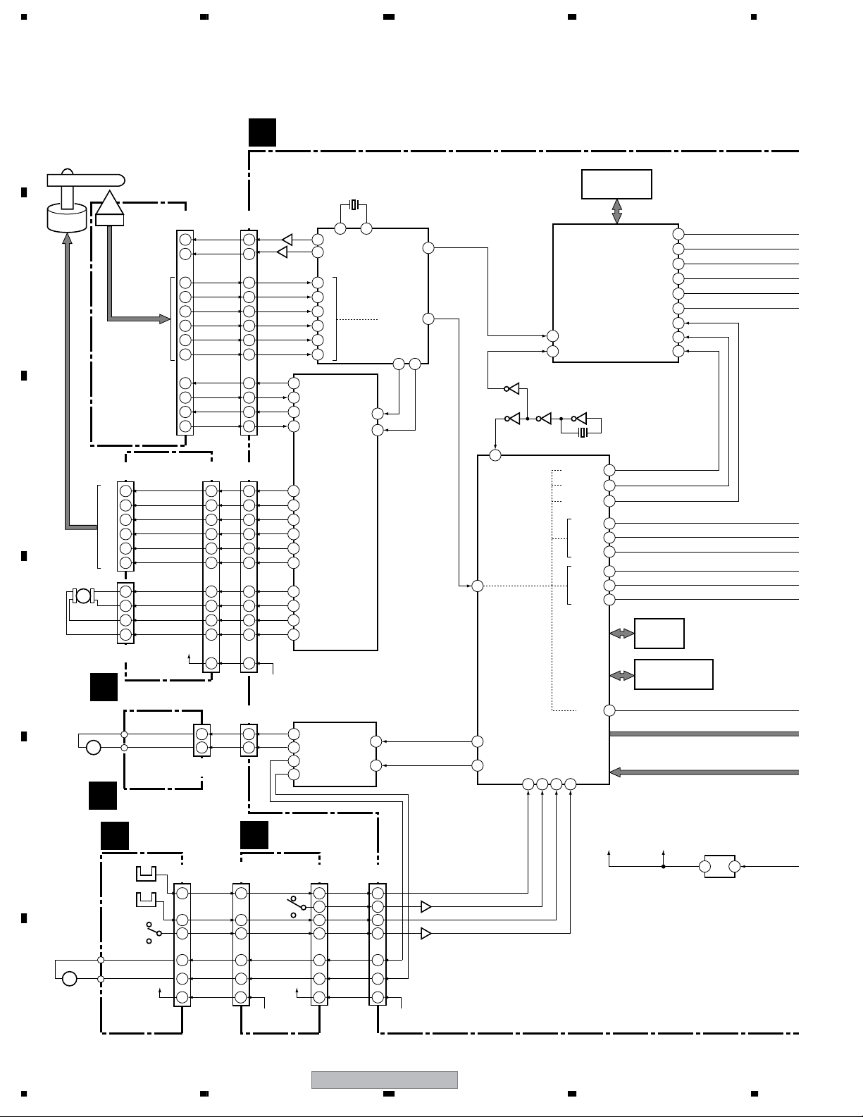
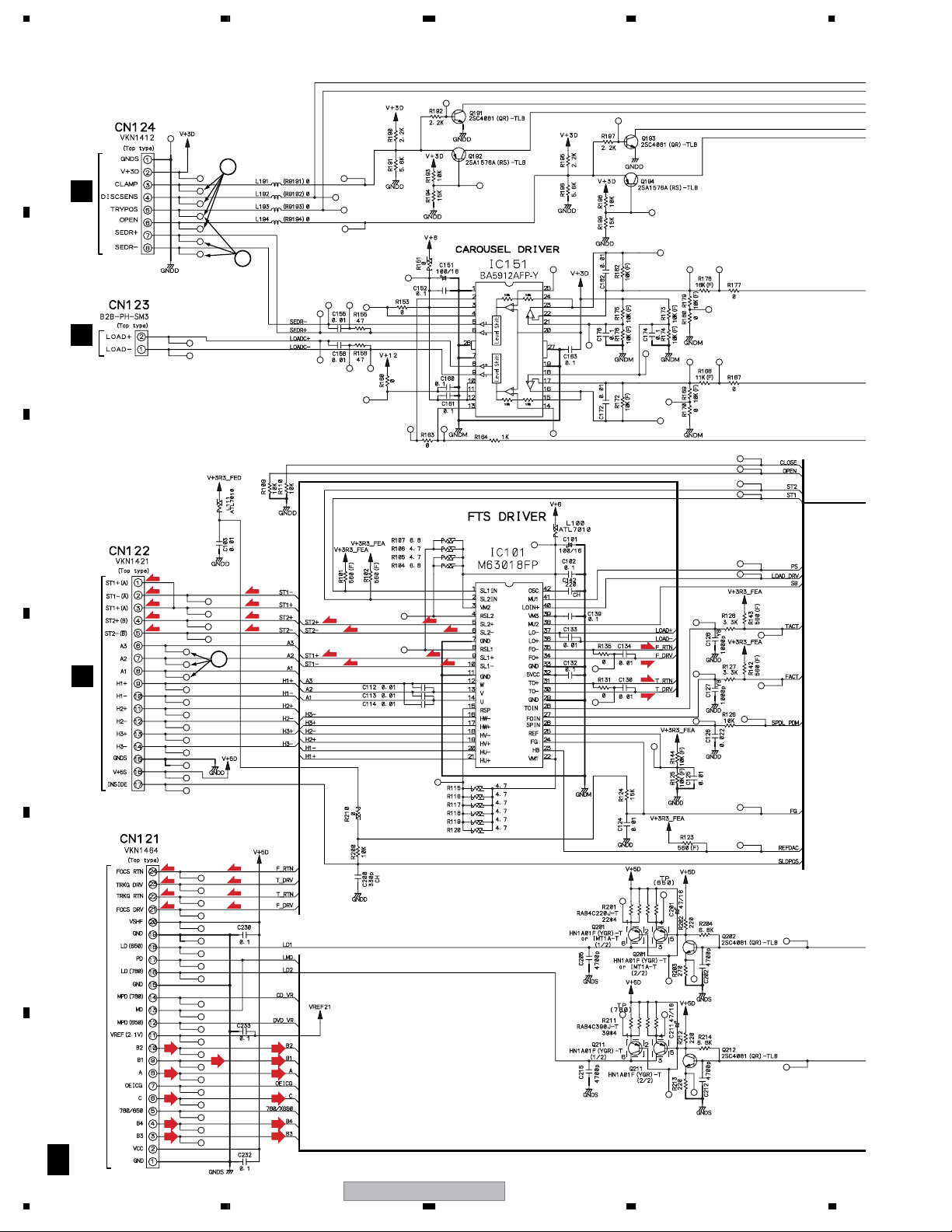
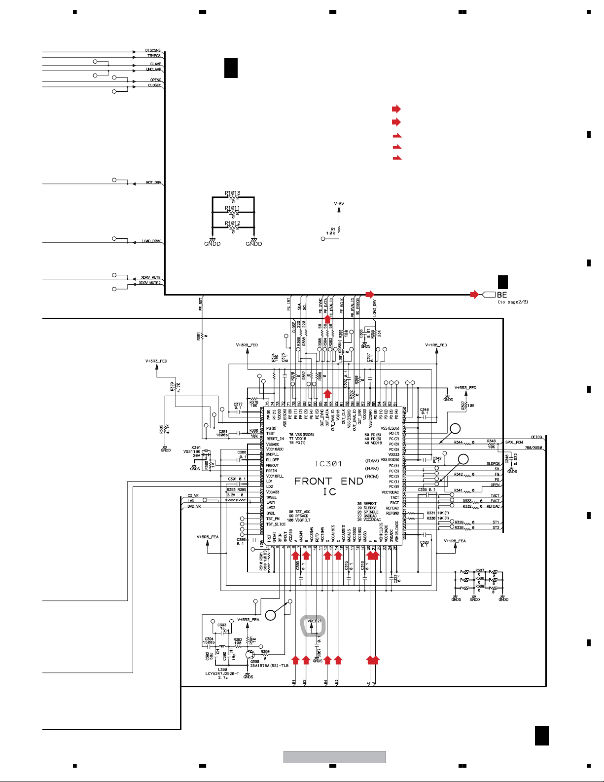
3. BLOCK DIAGRAM AND SCHEMATIC DIAGRAM
3.1 BLOCK DIAGRAM DVD SECTION
A
DVDM ASSYU(AWM7882)
A
X301
20MHz
B
C
D
E
F
SPINDLE
MOTOR
STEPPING
MOTOR
M
LOADING
MOTOR
+-
M
TRAY
MOTOR
OEIC
PICKUP
ASSY-S
CN1
(12P)
H1+
9
H1-
8
H2+
7
H2-
6
H3+
5
H3-
4
ST1+
ST1-
ST2+
2
ST2-
CN2
(4P)
G
SSIB ASSY
+–
M
J
LOMB ASSY
I
SSRB ASSY
PC21
PC22
S21
LOADING
POSITION
DET. SW
CN1013
(24P)
9
7
17
19
16
15
22
21
4
3
2
1
V+5S
CN31
CN21
(7P)
DISC SENS
5
TRAY POS
7
LOAD POS LOAD POS
3
6
4
+3.3V
2
LD (780)
LD (650)
A
C
B1
B2
B3
B4
TRKG DRV
TRKG RTN
FOCS DRV
FOCS RTN
CN3
(17P)
9
10
11
12
13
14
13
24
4
51
16
LOAD-
2
LOAD+
1
(2P)
SEDR+
SEDR-
V+3D
H1+
H1-
H2+
H2-
H3+
H3+
ST1+
ST1-
ST2+
ST2-
V+5S
CN121
(24P)
Q201,Q202
16
18
Q211,Q212
8
6
9
10
3
4
21
22
23
24
CN122
(17P)
9
10
11
12
13
14
1
2
4
5
16
V+5D
CN123
(2P)
1
2
H
TRSB ASSY
CN12
(7P)
S11
3
DISC
CLAMP
DET. SW
1
5
2
4
+3.3V
89
90
21
20
6
8
14
12
TO-
30
TO+
31
FO-
34
FO+
35
HU+
21
HU-
20
HV+
19
HV-
18
HW+
17
HW-
16
9
SL1+
10
SL1-
SL2+
5
SL2-
6
9
8
BA5912AFP-Y
6
Carousel Driver
5
CN11
(8P)
4
3
5
6
7
8
+3.3V
166
86 87
LD1
LD2
E
STM6316ATPAZ
F
A
B
C
D
SPIN
LOIN+
IC101
M63018FP
FTS Driver
IC151
DISC SENS
CLAMP
TRAY POS
SEDR+
SEDR-
V+3D
RFSACD
IC301
Front End IC
OUT_DATA
44 55
SPDL PDM
26
40
22
17
CN124
(8P)
4
3
5
6
7
8
16
V+3D
99
64
PC (6)
PD (0)
LOAD DRV
ROT DRV
LOAD DRVC
SACD_RF
Q191
Q193
FE DATA FE DATA
16
114
116
RF_SACD
SACD_27MHz
(1/3)
71
TC7WU04FU
120
PIXCLK
IC601
STI5588CVB
Back End IC
PWM2
PWM0
DISCSNS
SAA7893HL/C2
SACD IC
AGCINP
35
21
SYS_CLK
IC691
TC7WU04FU
PIO4[3]42PIO3[3]9PIO4[1]
PIO4[5]
CLAMP
TRYPOS
OPENC
(3/3)(2/3)
PCMDATA2
PCMDATA1
PCMDATA0
CV_OUT
40
OPENC
265 3
IC604
44
DISCSNS
CLAMP
TRYPOS
C_OUT
R_OUT
G_OUT
B_OUT
IC802
K4S641632F-TC75
64M SDRAM
DSD_PCM_0
DSD_PCM_1
IC801
Y_OUT
SPDIF
V+1R8_FED
DSD_PCM_2
DSD_PCM_3
DSD_PCM_4
DSD_PCM_5
PCM_LSRS_IN
PCM_LERI_IN
PCM_CELF_IN
X6401
27MHz
54
53
52
V
34
S_Y
32
S_C
33
R/Cr
27
G/Y
26
B/Cb
25
DOUT DOUT
57
DSD L/PCMDATA0
108
DSD R
109
DSD C/PCMDATA1
110
DSD LFE
111
DSD LS/PCMDATA2
113
DSD RS
114
40
39
41
IC603
VYW2182
Flash ROM
IC602
HY57V281620HCT
SDRAM
System Control
V+1R8_FEA
PQ018EZ01ZP
A DATA2
A DATA1
IC411
1.8V Reg.
A DATA0
V
S_Y
S_C
R/Cr
G/Y
B/Cb
13
16
XV-HTD540
1234
Page 17
5678
A
XV-HTD540
DAC L/D0
DAC R
DAC C/D1
DAC LFE
DAC LS/D2
DAC RS
V
S_Y
S_C
R/Cr
G/Y
B/Cb
Audio DAC (L, R)
PDATA
3
DSD_L
25
DSD_R
24
Audio DAC (Ls, Rs)
PCMDATA
4
DSD_L
1
DSD_R
2
Audio DAC (C, Lfe)
PCMDATA
4
DSD_L
1
DSD_R
2
Video Driver Amp.
V
4
S_Y
6
S_C
2
R/Cr
14
G/Y
10
B/Cb
12
IC851
DSD1791DBR
VOUTL+
VOUTL–
VOUTR+
VOUTR–
IC861
DSD1702EG
VOUTL
VOUTR
IC871
DSD1702EG
VOUTL
VOUTR
IC501
MM1623BF
V OUT
V IN
Y OUT
Y IN
C OUT
C IN
Cr OUT
Cr IN
CY OUT
CY IN
Cb OUT
Cb IN
IC741
17
18
13
12
9
10
9
10
BA4560F-HT
Audio LPF & Amp.
5
7
2/2
6
3
1
1/2
2
IC761
BA4560F-HT
Audio LPF & Amp.
3
1
1/2
2
6
7
2/2
5
IC781
BA4560F-HT
Audio LPF & Amp.
3
1
1/2
2
6
7
2/2
5
CN953
(30P)
11
FL
1
FR
3
SL
9
SR
C
5
LFE
7
CN5105
D
B
C
V
23
S_Y
21
S_C
26
R/Cr
16
G/Y
20
B/Cb
18
V
28
S_Y
30
S_C
26
R/Cr
24
G/Y
20
B/Cb
22
T
DOUT
IC901
TC74VHCT125AFT
IC421
13
3V → 5V Converter
IC911
TC74VHC08FT
5V → 3V Converter
V+3R3V+3R3_FEDV+3R3_FEA
V+3D
VDVD+12V+12
Q451
IC401
R1224N102H
3.3V Reg.
IC431
MM1565AF
V+5
V+5VV+5D
V+6
5V Reg.
IC441
PQ20WZ11
6V Reg.
VPR+8
63
71
VPR+8M
13
System Control System Control System Control
V+1R8_BE
PQ018EH01ZP
1.8V Reg.
21
30
29
28
27
26
CN911
(30P)
DOUT
VDVD+12
VPR+8
VPR+8
VPR+8M
VPR+8M
21
30
29
28
27
26
CN5107
(30P)
DVD TRADE ASSY
DOUT
VDVD+12
VPR+8
VPR+8M
19
CN5106
(19P)
CN5108
(4P)
2
1
2
DOUT
VDVD+12
VPR+8
VPR+8M
D
D
CN5104
E
D
J5105
F
56
XV-HTD540
17
7
8
Page 18
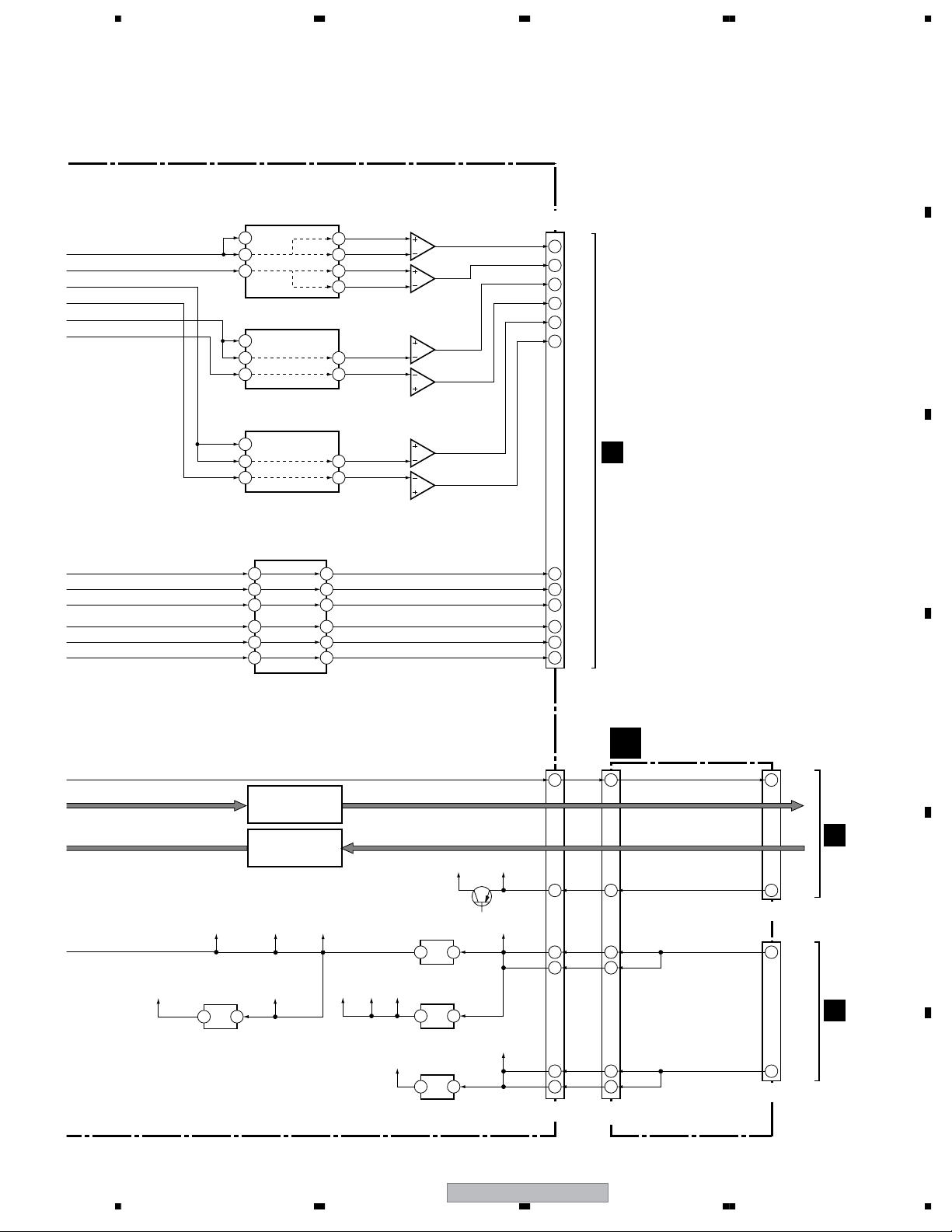
1234
3.2 BLOCK DIAGRAM MAIN SECTION
A
B
C
A
CN923
A
CN911
AUDIO
IN
VDVD+12
VPR+8M
VPR+8M
LINE1
AF ASSY
D
CN5102
(18P)
S_Y
18
S_C
14
V
16 9
R/Cr
12
B/Cb
10
G/Y
8
CN5101
(30P)
DOUT
21
30
VPR+8
29
28
27
26
JA3001
(1/2)
VDVD+12
VPR+8
VPR+8
TV
L
R
L
R
CN5103
(17P)
S_Y
11
S_C
7
V
R/Cr
5
B/Cb
3
G/Y
1
IC3001
BU4052BCF
Audio Input Select
11
4
15 13
14
5
32
O
CN8001
(18P)
11
7
9
5
3
1
IC3003
NJM4558MD
Buffer
3
2
VIDEO JACK ASSY
CN8852
S-VIDEO OUT
VIDEO OUT
CR
COMPONENT
CB
VIDEO OUT
Y
JA8851
(1/2)
1
Q3009,Q3005
6dB/10dB Attenuator
VIDEO
IC5501
PDC113A
System µ-com
HPL
DOUT
CN201
FM/AM TUNER
MODULE
D
K
E
AC IN
NEUTRAL
F
PRIMARY
ASSY
AN1
LIVE
1
2
J52
(8P)
VE+56
3 3
T1
CN1
1
POWER TRANSFORMER
2
(13P)
6
8
7
Lch
Rch
+9V
VFDP
VH
GND
VH
VL
VL
AC5V
AC5V
FLAC
FLAC
CN5701
(13P)
6
8
7
VX+9
CN52(8P)
CN11
(10P)
1
2
3
4
5
6
7
8
9
10
VE+56
VFDP
VH
VH
VL
VL
AC5V
AC5V
FLAC2
FLAC1
IC3101 (1/2)
NJM4558MD
LPF & Gain
2
1
3
IC3131 (1/2)
NJM4558MD
LPF & Gain
2
1
3
IC3161 (1/2)
NJM4558MD
LPF & Gain
2
1
3
IC3161 (2/2)
NJM4558MD
LPF & Gain
5
7
6
IC3121
BU4066BCF
SW Mix / Gain
11 10
3 4
SW
LIN
FL
SL
C
SW
SBLO
HPL
FL
INN1
2
FLOUT
SLOUT
COUT
SWOUT
IC3181
E-VOL
OUT1
27
30
29
32
3
INN2
6
SL
SLIN
13
C
CIN
15
SWIN
9
FL
FLIN
19
BD3814FV
Andrew
6
5
5
6
3
2
2
3
IC3252 (2/2)
NJM4558MD
IC3201 (2/2)
NJM4558MD
7
IC3241 (2/2)
NJM4558MD
7
IC3261 (1/2)
NJM4558MD
1
5
1
6
IC3261 (2/2)
NJM4558MD
FLSW
SL
C
SW
7
SBLO
18
XV-HTD540
1234
Page 19
FLAC1
FLAC2
VD+5
VFDP
VE+5
VA+12
VA-12
5
6
IC3901 (2/2)
NJM4560M
HP Amp.
VD+5
VA+5
CN5711
7
CN5602
(23P)
22
23
19
CN5603
(23P)
4
2
8
6
12
10
16
14
20
18
5678
DISPLAY ASSY
(27P)
13
14
19
21
25
24
22
7
8
VA+5
VD+5
OPTIN
LIN
RIN
FLO
FRO
SLO
SRO
CO
SWO
SBLO
SBRO
FLAC1
FLAC2
VD+5
VFDP
VE+5
VA+12
VA-12
HPR
HPL
L
CN5721
(27P)
7
8
13
14
19
21
25
24
22
DSP TRADE
N
ASSY
CN5612
(23P)
VA+5
22
VD+5
23
19
CN5613
(23P)
4
2
8
6
12
10
16
14
20
18
FLAC1
FLAC2
VD+5
VFDP
VE+5
VA+12
VA-12
IC5651
HEF4794BT
LED Driver
MSM9202-01
JOG
KEY
SR
VD+5
VA+5
V5601
XAV3020
FL TUBE
IC5601
FL Driver
5951
Remote Sensor Unit
COAXIAL
CN5621
(13P)
VD+5
8
VD+5
9
VA+5
12
OPTIN
3
CN5623
(19P)
CN5622
(19P)
3
1
7
5
11
9
15
13
19
17
LIN
RIN
FL
FR
SL
SR
C
SW
SBL
SBR
VA-12
VA+12
VD+5
JA8103
IN
CN8003
(13P)
CN8011
(19P)
CN8007
(19P)
8
9
12
3
3
1
7
5
11
9
15
13
19
17
CN5803
(13P)
11
10
2
8
6
V5D1
V5A
VA-12
VA+12
VD+5
HPR
HPL
J5801
(13P)
AK4114VQ
DIR & DIT
RX0
43
RX7
7
28
LIN
31
RIN
32
LOUT1
27
ROUT1
28
LOUT2
25
ROUT2
26
LOUT3
23
ROUT3
24
LOUT4
21
ROUT4
22
R
HP MIC
ASSY
VA-12
11
VA+12
10
VD+5
2
8
6
DSP ASSY
B
IC8201
FDTI
SDTO
25
IC8701
TC74LVX244FT
5V > 3V Converter
AK4529VQ
8ch CODEC
JA3901
PHONES
J5803
(5P)
IC8501
DSPD56367PV150
DSP
SDI1
10
SDO0
SDO1
SDO2
4 5 6 7
FDTO
SDTO
CDTO
66
7 8 12
SDTI1
SDTI2
IC8401
P
FUNCTION
KEY
ASSY
KEY KEY
IC8901
NJM2391DL1-33
3V Reg.
V5D1
IC8902
NJU7223DL1-18
1.8V Reg.
V5D1
BDTO
SDTI3
SDO3
SDTI4
31
12
J5805
(4P)
V3D
V1R8
JOG ASSY
S
DISC KEY
Q
ASSY
JOG
J5811
(3P)
A
B
C
D
UN+8V
VD+5
VA-12
VP+15
VPR+8
CN3032
(23P)
14
17
20
21
18
19
2
3
8
9
10
22
23
FLIN
FRIN
SLIN
SRIN
CIN
SWIN
UN+8V
UN+8V
VD+5
VA-12
VP+15
VPR+8
VPR+8
CN3012
(23P)
14
17
20
21
18
19
2
3
8
9
10
22
23
CN3022
(23P)
14
17
20
21
18
19
2
3
8
9
10
22
23
FLIN
FRIN
SLIN
SRIN
CIN
SWIN
UN+8V
UN+8V
VD+5
VA-12
VP+15
VPR+8
VPR+8
CN3002
(23P)
14
17
20
21
18
19
2
3
8
9
10
22
23
UN+8V
VD+5
VA-12
VP+15
VPR+8
CH1 IN
1
CH2 IN
15
CH3 IN
16
IC3301
STK402-270
Power Amp.
CH1 IN
1
CH2 IN
15
CH3 IN
16
IC3401
STK402-270
Power Amp.
CH1+VE
CH2+VE
CH3+VE
CH1+VE
CH2+VE
CH3+VE
6
10
18
6
10
18
VH+
VH-
CN3001
(23P)
7
8
3
4
22
23
18
19
14
15
10
11
12
13
1
2
FLOUT
FLOUT
FROUT
FROUT
SLOUT
SLOUT
SROUT
SROUT
COUT
COUT
SWOUT
SWOUT
VH+
VH+
VHVH-
M
6CH AMP ASSY
AMP TRADE
ASSY (1/2)
56
C
M
XV-HTD540
CN3021
(23P)
CN3011
(23P)
7
8
3
4
22
23
18
19
14
15
10
11
12
13
1
2
22
23
18
19
14
15
10
11
12
13
7
8
3
4
SWOUT
SWOUT
1
2
AMP TRADE
ASSY (2/2)
7
FLOUT
FLOUT
FROUT
FROUT
SLOUT
SLOUT
SROUT
SROUT
COUT
COUT
VH+
VH+
VHVH-
CN3031
(23P)
7
8
3
4
22
23
18
19
14
15
10
11
12
13
1
2
SBLO
VH+
VH-
IC3731 (2/2)
NJM4558MD
MIC MIX
5
7
6
JA3001
SBLO
CN3301
L
R
L
R
CENTER
SUBWOOFER
(1/2)
L
R
FRONT
SURROUND
LINE1
AUDIO
OUT
8
SPEAKER
E
F
19
Page 20
1234
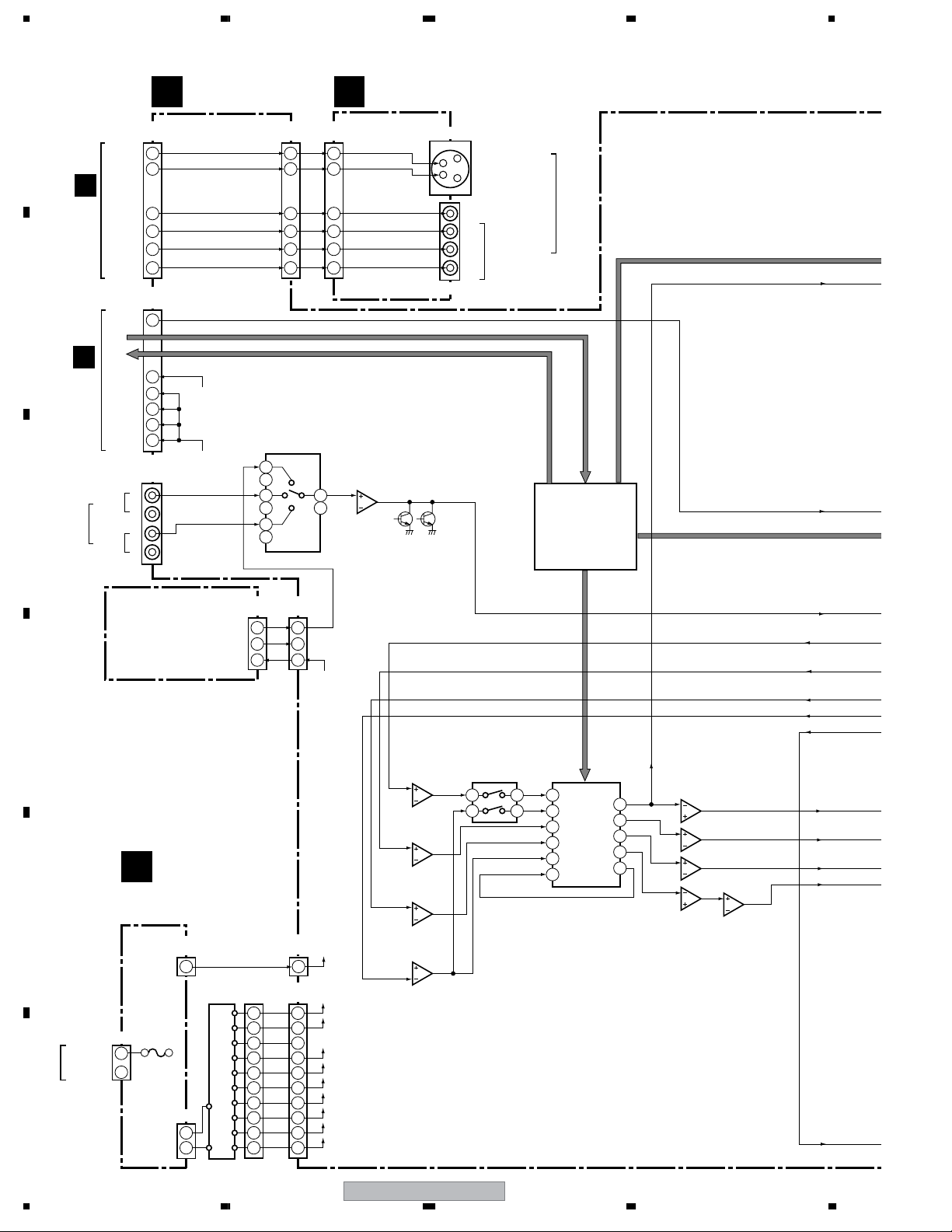
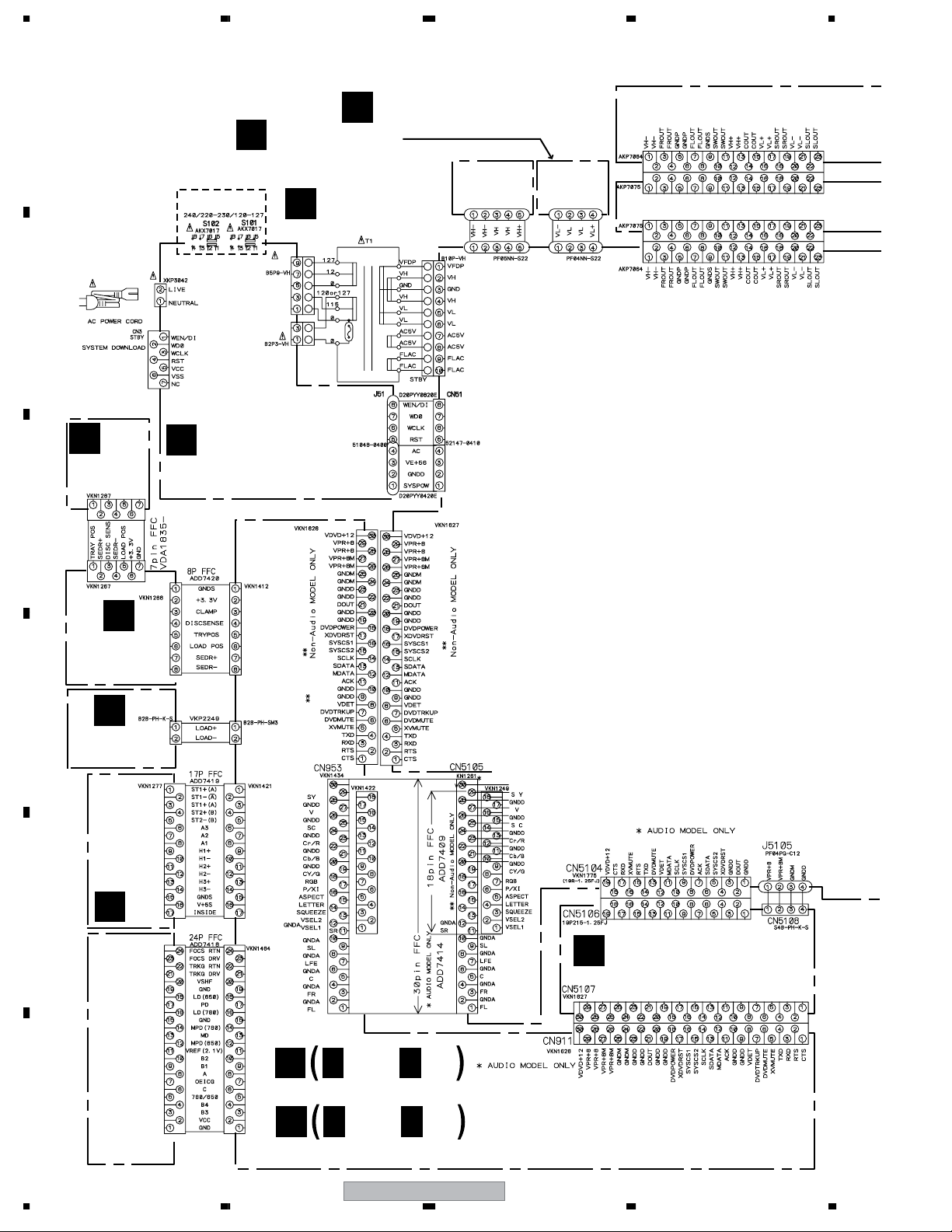
3.3 OVERALL WIRING DIAGRAM
A
B
C
I
SSRB ASSY
(XWZ3856)
CN21
DIODE L ASSY
E
(XWZ3840 :HTD540)
(XWZ3841 : DV8)
XV-DV8 Only
AN1
PRIMARY ASSY
K
F
CN2
CN1
(XWZ3844 : HTD540)
(XWZ3845 : DV8)
6CH AMP ASSY(AZW7283)
C
DIODE S ASSY
(XWZ3842)
J52
CN911
CN5101
CN52
J12
CN11
J21
CN3001
CN3021
CN3011
CN3031
CN124
CN12
CN11
H
TRSB ASSY
(XWZ3855)
D
J
CN31
LOMB ASSY
(XWZ3857)
CN3
SSIB ASSY
(XWZ3843)
E
G
CN1013
CN123
CN122
CN121
CN923
CN5102
DVD TRADE ASSY
T
(XWZ3858 : HTD540
Only)
A
A 1/4 - A 4/4
DVDM ASSY(AWM7882 : HTD540/KUCXJ Only)
F
PICKUP ASSY-S
(OXX8005)
A
A 1/3 - A 3/3
DVDM ASSY(AWM7881 : DV8 / Other)
20
1234
XV-HTD540
Page 21
5678
CN3651
CN3002
CN3022
CN3012
CN3032
D 1/4 - D 4/4
D
CN3301
AMP TRADE ASSY(XWZ3847)
M
JA3001
AF ASSY(XWZ3837 : HTD540/KUCXJ)
(XWZ3836 : DV8/Other)
CN5103
CN5701
A
B
VIDEO JACK ASSY(XWZ3849)
O
CN8001
C
CN201
CN5603
CN5613
CN5621
CN8003
NOTES: • When ordering service parts, be sure to refer to “EXPLODED
VIEWS and PARTS LIST” or “PCB PARTS LIST”.
• The > mark found on some component parts indicates the
importance of the safety factor of the part.
Therefore, when replacing, be sure to use parts of identical
designation.
• : The power supply is shown with the marked box.
CN5602
CN5612
DSP TRADE ASSY(XWZ3848)
N
CN5622
CN5623
JOG ASSY
(XWZ3854)
CN8007
B
CN8011
B 1/2 - B 2/2
S
DSP ASSY(AWX8523)
CN5711
CN5721
CN5803
DISPLAY ASSY
L
(XWZ3846)
HP MIC ASSY
R
(XWZ3852
:HTD540)
(XWZ3853
:DV8)
J5803
J5805J5811
Q
DISC KEY ASSY
(XWZ3851)
FM/AM TUNER UNIT
(AXX7172 : HTD540)
(AXX7173 : DV8)
J5801
P
FUNC KEY ASSY
(XWZ3850)
D
E
F
56
XV-HTD540
21
7
8
Page 22
1234
3.4 DVDM ASSY (1/4)
A
H
CN11
B
J
CN31
7
6
C
(S)
(S)
(S)
(S)
(S)
G
CN3
(S)
(S)
(S)
(S)
4
(S)
(S)
(S)
(S)
(S)
(S)
(S)
(S)
(F)
(F)
(T)
(T)
D
(F)
(T)
(T)
E
(F)
(F)
(T)
(T)
(F)
F
22
CN1013
PICKUP ASSY-S
A 1/4
1234
(RF)
(RF)
(RF)
(RF)
(RF)
(RF)
(RF)
(RF)
(RF)
(RF)
(RF)
(RF)
XV-HTD540
Page 23
(F)
(DVD)
(RF)
(T)
(S)
5678
A 1/4
DVDM ASSY (AWM7882 : HTD540)
(AWM7881 : DV8/Other)
: RF SIGNAL ROUTE
: DVD DATA SIGNAL ROUTE
(DVD) (DVD)
(DVD)
: FOCUS SERVO LOOP LINE
: TRACKING SERVO LOOP LINE
: STEPPING SERVO LOOP LINE
A
B
A 2/4
C
(DVD)
3
2
STM6316ATPAZ
(RF)
(RF)
(RF)
(RF)
(RF)
(RF)
1
(RF)
(RF)
(RF)
(RF)
(RF)
(RF)
R1011
R1012
R1013
(TO CHASSIS
GND)
D
E
56
XV-HTD540
F
A 1/4
23
7
8
Page 24
1234
3.5 DVDM ASSY (2/4)
A
B
A 2/4
DVDM ASSY (AWM7882 : HTD540)
(AWM7881 : DV8/Other)
7
C
D
STM5589CVS-K
(AD) (AD) (AD)
E
(DVD)
(AD)
(AD)
F
24
A 2/4
(CV)
(C)
(Y)
(DVD)(DVD)
(DVD)
(CY/G)
(Cb/B)
(Cr/R)
XV-HTD540
1234
Page 25
5678
(DVD)
(Cr/R)
HY57V641620HGT-H
(AD) (AD) (AD)
(CY/G)
(Cb/B)
(Y)
(C)
(C/V)
(AD)
: DVD DATA SIGNAL ROUTE
: VIDEO SIGNAL ROUTE (Cr/R)
: VIDEO SIGNAL ROUTE (CY/G)
: VIDEO SIGNAL ROUTE (Cb/B)
: S VIDEO SIGNAL ROUTE (Y)
: S VIDEO SIGNAL ROUTE (Y)
: S VIDEO SIGNAL ROUTE (C/V)
: AUDIO DATA SIGNAL ROUTE
A
B
A 3/4
(C) (C)
(C/V) (C/V)
(Y) (Y)
(CY/G)
(CY/G)
(Cb/B)
(Cr/R)
(Cb/B)
(C)
(C/V)
(Y)
(C/V)
(CY/G)
(Cb/B)
(Cr/R) (Cr/R)
(C)
C
A 3/4
D
(C)(C)
(Y)
(C/V)
(Y)
(CY/G)
(Cb/B)
(Cr/R)
(C/V)
(CY/G)
(Cb/B)
(Cr/R)
(Y)
E
A 3/4
56
XV-HTD540
F
(DVD)(DVD)(DVD)
A 1/4
A 2/4
25
7
8
Page 26
1234
3.6 DVDM ASSY (3/4)
A
B
C
RSQ035P03
RSX201L-30
3V REG.
(AD)(AD)(AD)
A 2/4
D
E
F
A 3/4
26
XV-HTD540
1234
Page 27
5678
A 3/4
DVDM ASSY (AWM7882 : HTD540)
(AWM7881 : DV8/Other)
(AD)(AD)
(AD)
A 2/4
A
(AD)(AD)(AD)
T
B
CN5101 or CN5107
D 1/4
C
A 2/4
(Y)
(C/V)
(C)
(Cr/R)
(Cb/B)
(CY/G) (CY/G)
(Y)
(C/V)
(C)
(Cr/R)
(Cb/B)
(Y)
12
8
13
11
9
10
(C/V)
(C)
(Cr/R)
(Cb/B)
(CY/G)
(C/V)
(Cr/R)
(Cb/B)
(CY/G)
(Y)
(C)
D
CN5102 : DV8 Only
D 1/4
E
(Cr/R)
: VIDEO SIGNAL ROUTE (Cr/R)
(CY/G)
: VIDEO SIGNAL ROUTE (CY/G)
(Cb/B)
: VIDEO SIGNAL ROUTE (Cb/B)
(Y)
: S VIDEO SIGNAL ROUTE (Y)
(C)
: S VIDEO SIGNAL ROUTE (Y)
(C/V)
: S VIDEO SIGNAL ROUTE (C/V)
(AD)
: AUDIO DATA SIGNAL ROUTE
56
XV-HTD540
F
A 3/4
27
7
8
Page 28
1234
3.7 DVDM ASSY (4/4) HTD540 Only
A
A 3/4
A 2/4
B
C
D
E
(FL)
(C)
(SW)
(SL)
(AD)
A 2/4
A 2/4, 3/4
A 2/4
A 1/4
F
A 4/4
28
(AD) (AD)
(AD) (AD) (AD)
XV-HTD540
1234
Page 29
5678
(FL) (FL)
(FL)
(FL)
(C)
(SW)
(FL)
(FL)
(FL)
(FL)
A 2/4
(C)
(SW)
(SL)
A 2/4
A 4/4
(FL)
(C)
(SW)
(SL)
DVDM ASSY (AWM7882)
HTD540 : Only
(FL)
(C)
(SW)
(SL)
9
10
(CY/G)
(Cb/B)
(Cr/R)
(C)
(C/V)
(Y)
11
13
8
12
A
B
CN5105
D 1/4
C
(SL)
(SW)
(C)
(SL)
(SW)
(SL)
(C)
(SW)
(SL)
(SW)
(SL)
(Cr/R)
: VIDEO SIGNAL ROUTE (Cr/R)
(CY/G)
: VIDEO SIGNAL ROUTE (CY/G)
(Cb/B)
: VIDEO SIGNAL ROUTE (Cb/B)
(Y)
: S VIDEO SIGNAL ROUTE (Y)
(C)
: S VIDEO SIGNAL ROUTE (Y)
(C/V)
: S VIDEO SIGNAL ROUTE (C/V)
(AD)
: AUDIO DATA SIGNAL ROUTE
(FL)
: AUDIO SIGNAL ROUTE (Front L ch)
(SL)
: AUDIO SIGNAL ROUTE (Surround L ch)
(C)
: AUDIO SIGNAL ROUTE (Center ch)
(SW)
: AUDIO SIGNAL ROUTE (Sub Woofer ch)
D
E
56
XV-HTD540
F
A 4/4
29
7
8
Page 30
1234
3.8 DSP ASSY (1/2)
A
B
C
B 1/2
DSP ASSY (AWX8523)
(L2) (L2) (L2)
(L2)
(AD)
(AD)
D
(AD)
(AD)
(AD)(AD)
B 2/2
E
(AD)
F
30
B 1/2
B 2/2
1234
B 2/2
XV-HTD540
Page 31

5678
(AD)
: AUDIO DATA SIGNAL ROUTE
(L2)
: AUDIO SIGNAL ROUTE (LINE 2 COAXIAL)
(FL)
: AUDIO SIGNAL ROUTE (Front L ch)
(SL)
: AUDIO SIGNAL ROUTE (Surround L ch)
(C)
: AUDIO SIGNAL ROUTE (Center ch)
(SW)
: AUDIO SIGNAL ROUTE (Sub Woofer ch)
A
(AD)
(AD)
(AD)
(AD)
(AD)
(FL)
(SL)
(SW)
(FL)
(C)
(FL)
(SL)
(SW)
(C)
B
(FL)
CN5622
N
C
D
(AD)
(AD)(AD)
N
CN5621
(AD)
XV-HTD540
56
E
F
B 1/2
31
7
8
Page 32

1234
3.9 DSP ASSY (2/2)
A
B
C
B 2/2
DSP ASSY (AWX8523)
B 1/2
(AD)
(AD)
(AD)
(AD) (AD)
(AD)
(AD)
(AD)
(AD)
D
B 1/2
B 1/2
E
CN5623
F
N
B 2/2
32
XV-HTD540
1234
Page 33

5678
(AD)
: AUDIO DATA SIGNAL ROUTE
A
B
C
D
E
56
XV-HTD540
F
B 2/2
33
7
8
Page 34

1234
3.10 6CH AMP ASSY
A
To
DC FAN
MOTOR
C
6CH AMP ASSY (AZW7283)
2
B
C
D
CN3021
M
CN3022
M
(SL)
(SW)
(FL)
(C)
(SL)
(FL)
(SW)(SW)
(C)
5
(SL)
(FL)(FL)
(SW)
(C)(C)
(SL)
(C)
(FL)
(SL)
(SW)
E
(FL)
(C)
(SL)
F
(SW)
3
(FL)
(C)
(SL)
(SW)
(FL)
(C)
(SL)
(SW)
C
34
1234
XV-HTD540
Page 35

5678
(FL)
: AUDIO SIGNAL ROUTE (Front L ch)
(SL)
: AUDIO SIGNAL ROUTE (Surround L ch)
(C)
: AUDIO SIGNAL ROUTE (Center ch)
(SW)
: AUDIO SIGNAL ROUTE (Sub Woofer ch)
A
B
(FL) (FL) (FL)
(FL)
(C) (C)
(C)
(SL) (SL)
(FL)
(SL)
(C)
(SL)
(C)
(FL)
(SL)
(FL)
(C)
(C)
(SW)
(SL)
(SW)
(C)
(C)
(SW)
(C)
C
(FL)
D
E
(FL)
(C)
(SL)
(SW)
(SW)
(SW)
(SW)
: Refer to 7. 1.12
56
XV-HTD540
(SW)
F
C
35
7
8
Page 36

1234
3.11 AF ASSY (1/4) and DVD TRADE ASSY(HTD540 Only)
A
D 1/4
AF ASSY (XWZ3837 : HTD540)
(XWZ3836 : DV8)
B
R5589 :47k DV8
R5532 :47k HTD540
C
CN5603
(FL)
(FL)
D
CN5613
N
CN5602
E
(SL)
(SW)
(C)
CN5612
N
F
36
D 1/4
(AD)
(FL)
XV-HTD540
1234
(AD)
Page 37

5678
CN911
A
A
CN5711
(FL)
T
DVD TRADE
ASSY
(XWZ3858)
HTD540
(AD)
CN5721
L
(SW)
(SL)
Only
(C)
D 4/4
D 2/4
(C)
(Cr/R)
: VIDEO SIGNAL ROUTE (Cr/R)
(CY/G)
: VIDEO SIGNAL ROUTE (CY/G)
(Cb/B)
: VIDEO SIGNAL ROUTE (Cb/B)
(Y)
: S VIDEO SIGNAL ROUTE (Y)
(C)
: S VIDEO SIGNAL ROUTE (Y)
(C/V)
: S VIDEO SIGNAL ROUTE (C/V)
D 3/4
CN5101
CN911
A 3/3
B
C
(AD)
D 2/4-4/4
D 2/4,3/4
(C)
CN52
K
J52
(FL)
(Cb/B)
(CY/G)
(AD)
(FL)
(FL)
(FL)
(C)
(Cr/R)
CN8001
O
: AUDIO DATA SIGNAL ROUTE
: AUDIO SIGNAL ROUTE (Front L ch)
(SW)
(SL)
(C)
(SL)
(V)
(Y)
(SW)
(SW)
CN5103
(SL)
(C)
(SW)
XV-HTD540
56
(AD)
(Y)
(V)
(C)
(Cr/R)
(Cb/B)
(CY/G)
(AD)
(SL)
(C)
(SW)
: AUDIO SIGNAL ROUTE (Surround L ch)
: AUDIO SIGNAL ROUTE (Center ch)
: AUDIO SIGNAL ROUTE (Sub Woofer ch)
7
CN5102
D 1/4
8
D
CN923 or CN953
E
A 3/3
F
T
37
Page 38

1234
3.12 AF ASSY (2/4)
A
(FL)
B
C
(FL)
(SL)
(FL)
(SL)
(SL)
(FL)
(SW)
(SL)
D
D 1/4
E
F
(C)
(SW)
D 1/4,3/4
(C)
(FL)
(SW)
D 2/4
38
XV-HTD540
1234
Page 39

D 2/4
5678
(FL)
AF ASSY (XWZ3837 : HTD540)
(XWZ3836 : DV8)
: AUDIO SIGNAL ROUTE (Front L ch)
(SL)
: AUDIO SIGNAL ROUTE (Surround L ch)
(C)
: AUDIO SIGNAL ROUTE (Center ch)
(SW)
: AUDIO SIGNAL ROUTE (Sub Woofer ch)
A
D 1/4,3/4,4/4
(FL)
1.2k
12k
0.1
0.1
B
(SW)
(SL)
(FL)
(C)
(FL)
1.2k
680
680
1k
0.068
0.068
1800p
1800p
1800p
39k
39k
39k
12k
C
(SL)
220
220
D
(C)
220
1000p
6.8k
56k
10k
47k
47k
0.033
XV-HTD540
56
E
(SW)
D 4/4
F
D 2/4
39
7
8
Page 40

1234
3.13 AF(3/4) ASSY
A
JA3001
(TV)
(TV)
(L1)
(FL)
(L1)
B
(FL)
(FL)
C
D
(TX)
E
F
40
(TX)
(FL)
(FL)
D 1/4
D 3/4
XV-HTD540
1234
Page 41

5678
D 3/4
AF ASSY (XWZ3837 : HTD540)
(XWZ3836 : DV8)
(FL)
(FL)
: AUDIO SIGNAL ROUTE (Front L ch)
(TV)
: AUDIO SIGNAL ROUTE (TV L ch)
(L1)
: AUDIO SIGNAL ROUTE (LINE 1 L ch)
(TX)
: AUDIO SIGNAL ROUTE (Tuner L ch)
A
D 1/4,2/4
B
(TX)
(TX)
C
D
CN5701
E
56
XV-HTD540
MODULE
To FM/AM TUNER
D 1/4,2/4,4/4
F
D 3/4
41
7
8
Page 42

1234
3.14 AF(4/4), DIODE L and DIODE S ASSYS
A
J12A
J21A
J12 J21
F
DIODE S ASSY
B
C
(XWZ3842)
CN3031
CN3021
(FL)
(SW)
(C)
M
DIODE L ASSY
E
(XWZ3840 :HTD540)
(XWZ3841 :DV8)
D
E
CN3032
CN3022
M
D 2/4
D 1/4-3/4
D 1/4
(SL)
(FL)
(SW)
(SL)
(C)
5
2
F
42
D 4/4
E F
XV-HTD540
1234
Page 43

5678
D 4/4
AF ASSY (XWZ3837 : HTD540)
(XWZ3836 : DV8)
(FL)
1
7
(SW)
1
(C)
(FL)
(SW)
(C)
(SW)
(FL)
: AUDIO SIGNAL ROUTE (Front L ch)
(SL)
: AUDIO SIGNAL ROUTE (Surround L ch)
(C)
: AUDIO SIGNAL ROUTE (Center ch)
(SW)
: AUDIO SIGNAL ROUTE (Sub Woofer ch)
(FL)
(SW)
(C)
(SL)
(FL)
A
B
CN3301
C
6ch SPEAKER OUT
(SL) (SL)
7
1
7
1
4
D
7
E
: Refer to "7. 1.12
PROTECTION CIRCUIT"
XV-HTD540
56
F
D 4/4
43
7
8
Page 44

1234
3.15 TRSB, SSRB, LOMB and SSIB ASSYS
A
TRSB ASSY (XWZ3855)
H
CN11
B
CN124
A 1/3
CN12
CN21
C
(S)
: STEPPING SERVO LOOP LINE
D
SSIB ASSY (XWZ3843)
G
CN1
SPINDLE MOTOR
E
: VXM1099
CN122
F
G H I
44
A 1/3
CN3
CN2
XV-HTD540
1234
STEPPING MOTOR
: VXM1101
(S)
(S)
(S)
(S)
Page 45

5678
SSRB ASSY (XWZ3856)
I
A
B
C
D
E
CN31
CN123
A 1/3
XV-HTD540
56
J
LOMB ASSY (XWZ3857)
7
F
I J
45
8
Page 46

1234
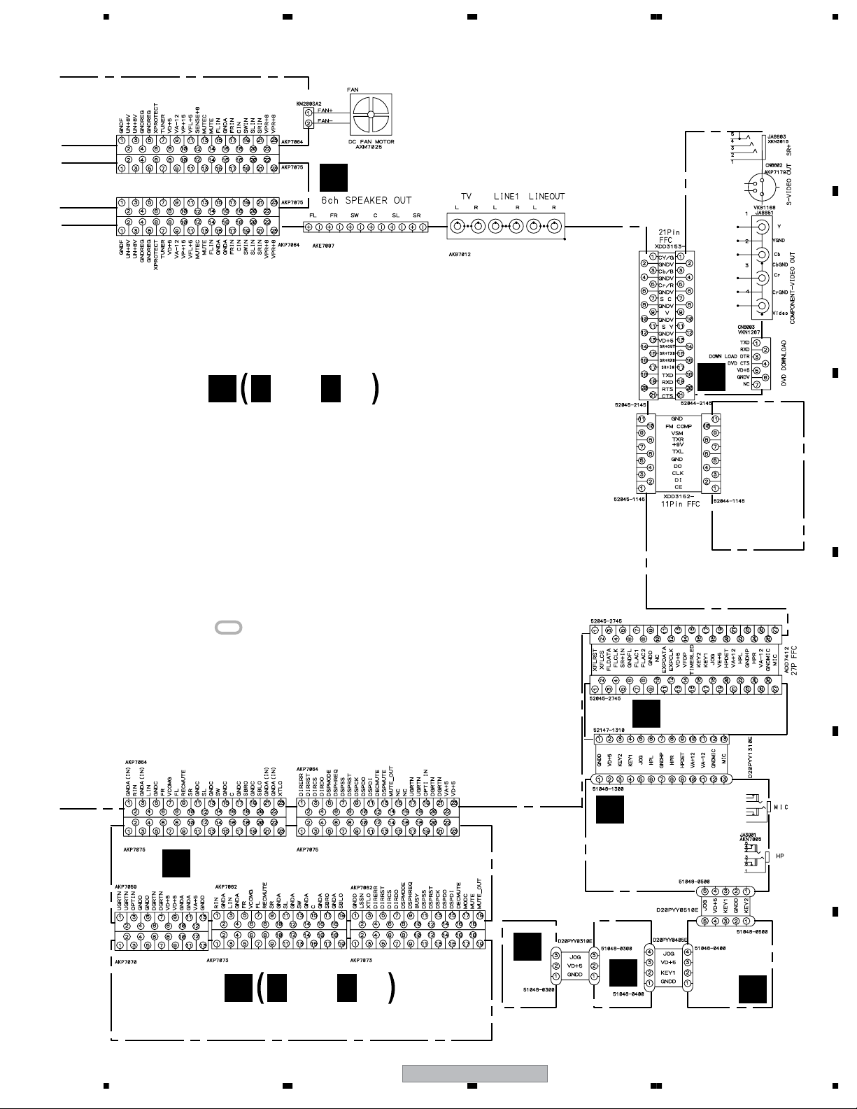
3.16 PRIMARY, AMP TRADE, DSP TRADE and VIDEO JACK ASSYS
CN5621
A
CN3011
CN3021
CN8003
(AD)
CN5613
CN5612
N
DSP TRADE ASSY
(XWZ3848)
CN5603
D 1/4
CN5602
D 1/4
B 1/2
(FL)
(SW)
CN3031
B
(C)
CN3001
C
D 4/4
(SL)
(FL)
CN3022
CN3002
C
CN3012
C
CN3032
D 4/4
(C)
(SW)
(SL)
CN5622
CN8007
B 1/2
CN5623
CN8011
B 1/2
(AD)
(FL)
(SL)
(SW)
(C)
D
E
(AD)
: AUDIO DATA SIGNAL ROUTE
(FL)
: AUDIO SIGNAL ROUTE (Front L ch)
(SL)
: AUDIO SIGNAL ROUTE (Surround L ch)
(C)
F
: AUDIO SIGNAL ROUTE (Center ch)
(SW)
: AUDIO SIGNAL ROUTE (Sub Woofer ch)
K M N
46
AMP TRADE ASSY
M
(XWZ3847)
CAUTION : FOR CONTINUED PROTECTION
AGAINST RISK OF FIRE.
REPLACE ONLY WITH SAME TYPE
NO. 491007 FOR IC25 MFD, BY
LITTELFUSE INC.
ADG7021 : KUCXJ
ADG1154 : DDXJ/RA,DLXJ/NC
ADG1158 : DDXJ/RB
ADG7099 : DPWXJ
REK1069: HTD540
(6.3A/125V)
AN1
/HTD540/KUC
/DV8/Other
K
(AD)
REK1029: DV8
(T5A/AL250V)
PRIMARY ASSY
(XWZ3844 : HTD540)
EXCEPT KUC
Model
HTD540/KUC
Only
(XWZ3845 : DV8/Other)
• NOTE FOR FUSE REPLACEMENT
CAUTION -
1234
FOR CONTINUED PROTECTION AGAINST RISK OF FIRE.
REPLACE WITH SAME TYPE AND RATINGS OF FUSE.
XV-HTD540
Page 47

5678
CN5103
D 1/4
(CY/G)
(Cb/B)
(Cr/R)
(C/V)
(Y)
(C)
JA8803
VIDEO JACK ASSY
O
(XWZ3849)
(CY/G)
: VIDEO SIGNAL ROUTE (CY/GR)
(Cb/B)
: VIDEO SIGNAL ROUTE (Cb/B)
(Cr/R)
: VIDEO SIGNAL ROUTE (Cr/R)
(Y)
(C)
(CY/G)
(Cb/B)
(Cr/R)
(C/V)
(Y)
: S VIDEO SIGNAL ROUTE (Y)
(C)
: S VIDEO SIGNAL ROUTE (Y)
(C/V)
: S VIDEO SIGNAL ROUTE (C/V)
CN8852
JA8851
A
B
C
KUCXJ
Only
CN8001
KUCXJ
Only
ATT7079 : HTD540
ATT7080 : DV8
CN2
CN1
ATS7354 : KUCXJ
ATS7355 : DV8/Other
D
CN11
D 4/4
E
CN52 or CN51
D 4/4
J52
STBY
XV-HTD540
56
F
OK
47
7
8
Page 48

1234
3.17 DISPLAY, FUNCTION KEY, DISC KEY, HP MIC and JOG ASSYS
A
B
DISPLAY ASSY
L
(XWZ3846)
C
D
E
CN5721
CN5711
D 1/4
(FL)
(FL)
JOG ASSY
F
L P S
48
J5811
(XWZ3854)
P
FUNC KEY ASSY(XWZ3850)
S
XV-HTD540
1234
Page 49

5678
JOG ASSY
S5861 : VOLUME UP ↔ DOWN
DISC KEY ASSY
S5841 : DISC 1
S5842 : DISC 2
S5843 : DISC 3
S5844 : DISC 4
S5845 : DISC 5
R
(FL)
: AUDIO SIGNAL ROUTE (Front L ch)
HP MIC ASSY
(XWZ3852 : HTD540)
(XWZ3853 : DV8/Other)
A
B
C
CN5803
(FL)
J5805
J5801
J5803
DISC KEY ASSY
Q
(XWZ3851)
(FL)
(FL)
HP MIC ASSY
S5831 : STAND BY/ON
FUNCTION KEY ASSY
S5851 : DVD/CD
S5852 : TUNER (FM/AM/ST.)
S5853 : TV/L1/L2
S5854 : 4 1 (REVERSE)
S5855 : ¡ ¢ (FORWARD)
S5856 : 7 (STOP)
S5857 : 6 (PLAY/PAUSE)
S5858 : DISC SKIP
S5846 : EXCHANGE
S5847 : OPEN/CLOSE (0)
D
E
F
56
XV-HTD540
RQPL
49
7
8
Page 50

1234
3.18 DVDM WAVEFORMS
A
DVDM ASSY
A
Note : The encircled numbers denote measuring point in the schematic diagram.
Measurement condition : No. 1 to 2 and 8 to 13 : reference A1 (DVD), T2-chp 19, Color -bar
IC301-pin 4 (RFOUT)
1
V: 200mV/div. H: 0.1µsec/div.
GND
IC301-pin 36 (FG)
2
V: 1V/div. H: 5msec/div.
B
IC301-pin 44 (SPDL_PDM)
3
[PLAY → STOP → PLAY] [PLAY]
Brakes
ON
PLAY
V: 2V/div. H: 1sec/div.
Accelerator
ON
PLAY PLAY
V: 2V/div. H: 500nsec/div. V: 2V/div. H: 500nsec/div.
C
[STOP]
CN122-pin 8, 7, 6
4
V: 2V/div. H: 2msec/div.
[PLAY]
(FTS Driver -A1, A2, A3)
CN124-pin 5 (TRAY POS)
6
CN124-pin 7, 8
(Rotating Tray Motor drive voltage)
DISC 2 DISC 3 DISC 4 DISC 5 DISC 5
D
CN124-pin 4, 5, 6, 3
7
IC601-pin 114
[Tray move] [Tray open]
CN124-pin 4 (DISC SENS),
CN124-pin 5 (TRAY POS)
E
V: 2V/div. H: 1sec/div.
CN923-pin 16 (Composite Video out)
8
V: 1V/div. H: 10µsec/div.
CN923-pin 8 (Component Video out-Y)
9
V: 1V/div. H: 10µsec/div.
CN923-pin 10 (Component Video out-Pb)
10
V: 2V/div. H: 10µsec/div.
CN923-pin 12 (Component Video out-Pr)
11
V: 2V/div. H: 10µsec/div.
[Tray close]
Rotary tray move
V: 2V/div. H: 500msec/div.
Elements on larger
Rotary tray stop
CN124-pin 6 (OPEN),
CN124-pin 3 (CLAMP)
Loading close
Clamp
V: 2V/div. H: 500msec/div. V: 2V/div. H: 10µsec/div.
Loading open
Unclamp
Rotary tray move
STOP
Right-hand
Left-hand
12
13
9
10
[Tray close]
Rotary tray stop
V: 2V/div. H: 200msec/div.
IC601-pin 114 (ROT_DRV)
CN923-pin 18 (S Video out-Y)
V: 1V/div. H: 10µsec/div.
CN923-pin 14 (S Video out-C)
V: 1V/div. H: 10µsec/div.
12
13
F
11
50
XV-HTD540
1234
Page 51

5678
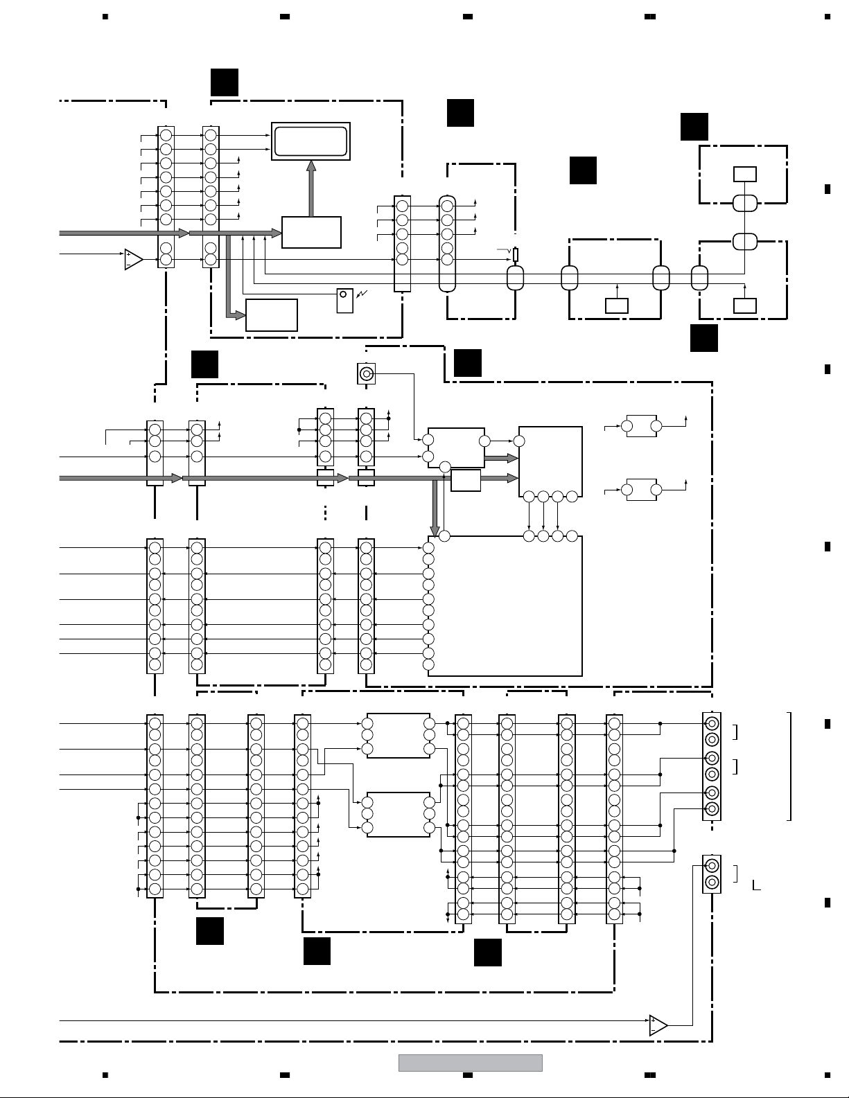
4. PCB CONNECTION DIAGRAM
NOTE FOR PCB DIAGRAMS :
1. Part numbers in PCB diagrams match those in the schematic
diagrams.
2. A comparison between the main parts of PCB and schematic
diagrams is shown below.
Symbol In PCB
Diagrams
BCE
BCE
D
Symbol In Schematic
Diagrams
BCEBCE
BCE
BCE
DGGSS
DGS
Part Name
Transistor
Transistor
with resistor
Field effect
transistor
Resistor array
3-terminal
regulator
3. The parts mounted on this PCB include all necessary parts for
several destinations.
For further information for respective destinations, be sure to
check with the schematic diagram.
4. View point of PCB diagrams.
Connector
Capacitor
SIDE A
P.C.Board
Chip Part
SIDE B
A
B
C
D
E
F
56
XV-HTD540
51
7
8
Page 52

1234
4.1 TRSB, SSRB and LOMB ASSYS
A
B
C
SIDE A
W21
W22
W23
S21
TRSB ASSY
H
TRSB
XWZ3855-
1.TRAY POS
5.LOAD POS
2.SEDR+
6.+3.3V
3.DISC SENS
7.GND
4.SEDR-
1
CN12
1
CN12
CN21
GND
7
+3.3V
W25
W24
5
PC21
DISC
SENSOR
1
4
2
CN21
3
W26
SSRB
XWZ3856-
FR1S
CN11
W11
7
W12
8.SEDR-
17
1
W27
GND
PC22
3
4
TRAY
POSITION
(XNP3082-B)
8
6.LOAD POS
7.SEDR+
CN11
8
4.DISC SENS
5.TRAY POS
7.TRAY POS
6.SEDR+
5.DISC SENS
4.SEDR-
3.LOAD POS
2.+3.3V
1.GND
2
1
1
1
1.GND
2.+3.3V73.CLAMP
(XNP3082-B)
CN124
A
W13
S11
GND
15
FR1S
TRSB ASSY
H
CMK-P3X
GND
R11
1
CLAMP SW
(XNP3082-B)
Black
Q22
Red
CMK-P3X
CN11
1
5
TRSB
1.TRAY POS
8
8.SEDR-
5.LOAD POS
6
5
51
8
7.SEDR+
2
2.+3.3V
4.DISC SENS
3.CLAMP
1.GND
6.LOAD POS
5.TRAY POS
5
CN12
TRAY
M
M
MOTOR
CN21
5.DISC SENS
3.LOAD POS 6.SEDR+
1.GND
17
7.TRAY POS
4.SEDR-
2.+3.3V
5
GND
C
Q22
TRAY
POSITION
E
R21
3
B
2
1
R25
R22
XWZ3856-
2
4
SSRB
R26
6
3
C21
C
XWZ3855-
2.SEDR+
3.DISC SENS
2
4.SEDR-
17
6.+3.3V 7.GND
+3.3V
4
2
1
BE
Q21
GND
R24
DISC
SENSOR
51
R23
(XNP3082-B)
SIDE B
5
POS SW
1
R27
SSRB ASSY
I
SSRB ASSY
I
D
LOMB ASSY
J
SIDE A
CN123
A
CN31
LOMB
XWZ3857-
1
CN31
2.LOAD-
1.LOAD+
E
1
FR1S
ROADING
MOTOR
CN31
Label Side
1
C31
LOADING MOTOR
CMK-P3X
1.LOAD+
SIDE B
2.LOAD-
M
+
(XNP3082-B)
F
+
LOMB
XWZ3857-
(XNP3082-B)
H I J H I J
52
1234
XV-HTD540
Page 53

5678
4.2 SSIB and DVD TRADE ASSYS
A
DVD TRADE ASSY
T
(HTD540 : Only)
DVD TRADE ASSY
T
CN5104
D
CN5106
J5105
D
CN5108
CN5107
CN5107
A
CN911
SIDE A
B
(XNP3081-B)
C
SIDE B
CN5106 CN5108
SIDE A
SSIB ASSY
G
CN2
M
(XNP3081-B)
1
1
Contact Side
A
CN2
4
4
CN3
1
1
CN3
CN122
ST1-A3ST2+
ST1-A3ST2+
[ST1+]
ST1+
ST1+
[ST1+]
Contact Side
Contact Side
ST2-
ST2-
V+5S
V+5S
A1
H1-
H3-
H2-
A1
H1-
H3-
H2-
SSIB
SSIB
INSIDE
INSIDE
H1+
A2
H2+
H1+
H2+
H3+
GNDS
A2
H3+
GNDS
XWZ3843-
CMK-P3X
12
17
17
12
1
1
Contact Side
Contact Side
CN1
CN1
SPINDLE
M
MOTOR
SSIB ASSY
G
SSIB
XWZ3843-
12
CN1
G T E
(XNP3081-B)
GND
C2
1
CMK-P3X
C1
17
CN3
4
1
SIDE B
1
CN2
(XNP3081-B)
G
T
XV-HTD540
56
7
8
D
E
F
53
Page 54

1234
4.3 DVDM ASSY (HTD540 Only)
A
B
C
D
E
F
SIDE A
A
IC901
Q192
Q201
Q390
IC441
Q401 Q929
IC411
Q761
IC421
DVDM ASSY
(XV-HTD540 Only)
30
30
C442
R443
R442
R441
C413
C412
C411
L411
C805
C806
R811
H
C409
R411
R1004
C443
IC441
D401
L402
C425
C481
A
Q451
D431
C451
C452
C431
R444
C441
R401
C404
C463
C414
F
R485
R481
75
7
IC481
1
C483
C484
R482
R1006
R1005
Q951
Q451
Q911
IC101
Q925
Q926
IC201
Q211
IC431
Q212Q202
Q193
IC301
Q923
IC401
Q922
Q921
Q927
Q928
Q930
Q722
IC461
IC604
Q763
Q762
IC691
IC601
Q782Q764
Q781
Q742
Q741
IC805
IC806
IC804
IC481
IC801
UP SIDE
30
CN901
R451
D432
R918
C902
R433
75
5
7
C433
R906
41
R908
41
IC431
C432
C403
R400
3
4
54
C407
A
R416
C462
IC411
IC461
C415
C621
L421
C423
C424
C422
IC421
C660
R839
R805
R808
R809
R806
C804
C827
IC806
1
3
R813
5
R812
4
R814
5
R815
4
41
R818
R895
R816
C482
R819
R820
C812
C803
C802
CN11
H
CN124
CN921
R983
R960
R961
R962
R921
14
C642
5
5
R826
C641
R803
R407
38
R837
D
C807
65
R984
Q925
CN124
Q926
R931
R922
R901
D925
D927
R151
R410
C151
D
R620
C644
C634
1
R610
C619
23
231
R673
C622
4
4
1
1
C640
13
R626
C636
4
IC691
156
5
IC601
C600
R600
R821
R822
R802
C601
D601
23
231
R801
R807
38
65
C813
C811
C808
R836
E
1
1
14
C901
R909
C434
C401
IC401
R409
R408
C491
C410
R462
L641
R461
224
2
8
C691
C692
L691
R698
224
2
R804
39
39
64
64
R827
R907
C421
C951
3
1
R881
7
IC901
8
1
C661
R640
IC604
R880
R817
R951
7
8
C408
R421
CN608
R810
24
R644
R838
C801
C461
CN609
X601
1
CN3
G
CN122
UP SIDE
1
12
1
12
1
R981
Q951
R963
8
8
L193
L194
R933
R932
R934
D926
C405
Q401
B
C311
C318
R693
R697
105
104
105
C607
C649
156
157
C659
CN607
1
129
2
2
R883
24
IC805
C814
R982
C312
C315
104
C830
C816
C815
1
1
10
IC801
R823
R953
R403
R924
R925
A
D402
SIDE
CONTACT
R954
R952
R955
R957
R199
Q193
Q923
R923
R926
D922
R402
C406
Q930
R938
R939
C307
R612
R613
C694
C671
E
C825
102
R956
R959
R196
Q922
SIDE
C310
R609
C690
1
R905
L192
C681
1
1
1
R197
C309
128
103
R958
C921
C303
C308
R696
R904
L191
LOAD-
102
H1-
1
1
CN122
R903
R902
CONTACT
LOAD+
Q921
R936
C698
C828
20
20
11
R825
128
C810
A3
A2
A1
H2+
H2-
H3+
R191
Q911
R194
SIDE
Q192
12
CN123
Q929
R937
R332
R333
R334
R341
R336
C
R337
R339
R340
C346
R675
C684
30
8
8
1
14
R824
R884
C809
1.INSIDE
1
H1+
1
CN105
GNDD
V+5S
H3-
C118
C120
R192
C102
C135
R123
21
R124
C121
C302
D923
R389
R935
D928
R338
R342
Q927
C
Q928
C301
C354
R344
R346
R398
R397
C664
R689
29
R686
30
E
R893
R888
R848
5
5
4
IC804
R886
R835
R834
R868
R828
R833
R832
R831
R830
R829
C132
R882
UP
R688
R887
C101
C342
21
C348
R847
R843
R844
C116
22
R658
C652
C824
J
17
17
R354
53
53
52
208157
208
R694
R687
R885
C860
CN31
CN123
B
4
4
CONTACT
SIDE
C113
C127
C128
C124
C126
IC301
C326
26
C335
50
R361
L361
R656
R657
R655
R652
52
R639
C648
C647
C630
C623
R628
C614
1
1
R685
R695
R664
C605
R684
R691
R692
C867
R894
C861
C864
C863
R869
CN104
1
1
ST2-
R102
C114
R101
C112
C133
C130
C323
C306
B
25
251
5026
51
R363
R654
R653
R364
R651
C650
R638
R648
R647
C637
R635
R641
R683
R682
R621
R681
C604
R619
R672
R603
R602
R605
C799
R879
C873
R878
PICKUP ASSY
24 1
24 1
24
231
23
ST1-
CN121
C221
IC101
R220
R221
R222
C222
C142
R223
42
R131
R135
C134
C390
R392
R391
RFOUT
RFIN
C300
1
100
R396
100
C388
76
7551
75
C373
R368
R369
R307
R309
R308
C357
R362
R360
C651
C564
R636
C1564
R561
R662
C1563
Q763
R768
R769
R767
R771
Q764
R788
R792
D782
R787
R791
R775
R760
R754
R770
R734
R739
C795
D781
R789
R738
R790
C877
C874
C870
R858
C851
C871
CN121
IC201
1
1
4
4
Q390
R390
C394
C392
R310
R302
NP
10 2
C305
C362
D761
R772
R756
D743
R753
R755
C798
R736
C850
9
BOTTOM SIDE
CN101
ST2+
ST1+
1
C139
R367
R365
R366
R637
R634
R629
R663
R665
R611
R608
R618
R617
R616
R607
R606
R889
R890
C750
BOTTOM SIDE
224
2
C103
1
51
SIDE
5
CONTACT
CN103
1
C231
R201
8
8
LD1
5
5
Q201
R202
L390
C393
Q202
R204
R214
R301
C202
R203
C304
C391
C383
R968
R111
R394
R969
R300
X301
C382
C377
R384
R383
R382
CN301
1092
R967
1
1
R966
R386
R378
R385
R379
Q722
R721
R722
R595
R594
C571
R571
R593
R592
R591
R590
R562
C1562
R1069
C561
Q762
Q761
Q782
Q781
Q742
CONTACT
SIDE
Q741
C797
D742
R737
C758
R859
D741
C857
C757
C854
R4
R2
R3
R1
R1003
SIDE A
C
1
W
S
D
3
+
V
2
W
S
+
D
A
O
-
L
D
A
O
L
V+5D
R211
GNDD
LD2
Q211
R212
Q212
C212
R213
C201
C211
CN904
11
11
1
1
SY
30
GNDD
V
GNDD
SC
R964
GNDD
Cr/R
R965
GNDD
Cb/B
GNDD
CY/G
20
RGB
P/XI
ASPECT
CN953
30
30
30
UP SIDE
1
1
1
CN943
D
R774
LETTER
C774
SQUEEZE
VSEL2
R773
VSEL1
C773
GNDA
R794
SR
C794
GNDA
R793
C793
SL
R758
GNDA
C756
LFE
R757
GNDA
C755
C
GNDA
C853
FR
GNDA
1 FL
R735
G
R1002
R1001
(VNP7480-A)
CN953
CN5105
D
54
A
A
XV-HTD540
1234
Page 55

5678
SIDE B
A
DVDM ASSY
CONTACT
SIDE
1
1
2
224
R1011
R1012
R1013
C232
R970
R972
R974
R976
15
28
C233
C215
C205
R393
R395
B
C
987654321
R373
R374
0
321
1
0
IC501
0
15
1528
28
28
C562
IC741
Q744
Q746
IC851
Q745
IC807
C521
C563
R521
R740
C501
R501
C511
R511
R977
IC761
C769
R779
C761
R759
8
IC781
5
14
141
1
1
3
C829
4
5
R109
UP SIDE
C743
R741
C214
R747
R745
NORMAL SOLDER
LEAD FREE SOLDER
R388
C204
C213
R387
R1970
C1051
C1052
C1053
C1054
C1055
C1056
R1056
R1057
R1058
R1059
R1060
R1061
R971
R973
R975
R751
C747
C751
R749
C741
C745
R743
R851
R856
R855
R854
R110
C203
CONTACT
SIDE
R765
C859
C858
C855
C852
R857
R850
R853
R852
R763
R761
A
1
0
C765
C763
C753
1
4
15
23
23
24
CN111
C230
C199
R305
R304
R303
R399
C381
R381
R380
R370
R376
D301
C565
14
114
1
1
4
C754
C791
F
R877
C876
C313
R375
R9531
R9551
R9541
R9521
R9501
R9511
C531
R531
R532
C551
R551
C541
R522
R541
R512
C771
Q977
C772
C766
8
1
11
1120
20
R874
R875
R876
HEAT-RESISITANCE
SIDE
R103
R106
R104
R107
R105
R108
R306
R330
R331
R343
R345
C355
R355
Q531
Q551
Q541
Q521
Q501
Q511
R533
R552
R553
R542
R543
R523
R503
R502
R513
R764
R766
C767
R762
C768
C762
C792
C789
8
11
1120
C866
20
R864
R865
10
C875
1
110
IC871
C872
R873
R872
R871
R870
CONTACT
R115
R116
R117
R328
R329
R674
C764
IC861
R866
R846
R845
17
R118
R119
R120
R128
R127
R143
R666
R604
10
1
110
R867
C787
C781
5
5
8
8
PRE-FLAX
17
C125
R125
R126
R142
R927
R660
R659
27
28
R601
C865
C862
R860
C788
C782
4
1
C826
R928
R699
R863
R862
R786
1
R210
R144
R661
R650
4
CN112
R929
C632
Q603
C786
C784
IC803
27
28
R649
SIDE B
A
CN5107
T
CN911
30
CLAMP
R164
R170R169
R1623
54
R783
C783
2
1
1
CN911
DISCSENS
TRYPOS
R160
R162
C161
13
14
14
C620
C628
1
1
IC602
54
25
241
C785
C822
C819
UP SIDE
30
30
2
D921
R915
SEDR-
OPEN
SEDR+
R914
CONTACT
71
1
7
IC911
SIDE
81
8
R161
R916
R154
R156
R159
R157
C155
R155
C158
R158
C160
26
26
13
27
27
C163
R179
C176
R176
R175
R173
C174
C602
IC603
R646
R178
R180
R615
R614
R623
R624
R627
C624
R625
R631
R622
C625
C643
R643
R645
R896
R841
R842
C820
C913
C912
8
14 8
14
C911
R917
R431
R432
R152
R153
C152
1
1
IC151
R405
R406
D403
25
25
R183
C182
R182
C181
R181
C177
R177
R642
R671
C626
C639
28
28
27
27
R483
C821
UP SIDE
CN931
CONTACT
SIDE
LF
CN941
1
1
C200
R200
C210
R113
R112
CN113
R189
R100
21
2
R930
D924
C633
C603
R630
R632
R633
R690
C903
R670
R784
R782
R861
V+3D
GNDS
R190
1
R193
CN114
Q191
R195
R198
Q194
1
R165
R163
Q924
R166
C172
R172
R171
C171
R168
C167
R167
R174
C635
C638
C627
C629
C631
48
D603
C749
C746
C748
R750
R752
R785
R781
C752
R744
R746
R748
C742
C744
R742
C823
C856
F
54
54
IC802
1
1
C818
R840
C817
R452
R913
R453
R912
1.CTS
RTS
RXD
TXD
R911
R404
DVDM ASSY
AWM7
R415
R422
FCICT
1
29
Q452
XVMUTE
SYS_CS1
C402
R414
UP SIDE
1
1
30
30
VDET
DVDMUTE
ZERO
DVDPOWER
XDVDRST
L401
0
00
0
1
11
1
2
22
2
3
33
3
4
44
4
4
5
55
5
6
66
6
7
77
7
7
8
88
8
9
99
9
R412
R417
R454
GNDD
10.GNDD
GNDD
20.GNDD
VPR+8M
00
11
22
33
4
55
66
7
88
99
R413
DOUT
VPR+8
ACK
GNDD
MDATA
GNDD
VPR+8
A-
Q452
IC911
Q191
SYS_CS2
SCLK
SDATA
30.VDVD+12
GNDM
GNDM
Q194
VPR+8M
Q924
IC151
Q531
Q551 Q541
Q521
Q501
Q511
IC501
IC602
Q603
Q977
IC603
Q745
Q746
IC761
Q744
IC781
IC741
IC802
IC803
IC851
IC871
IC807
(ANP7480-A)
B
C
D
IC861
E
F
A
56
XV-HTD540
A
55
7
8
Page 56

1234
4.4 DVDM ASSY (DV8 / Other)
SIDE A SIDE A
A
A
DVDM ASSY
G
CN3
(XV-DV8 Only)
PICKUP ASSY
CN121
H
CN11
CN122
J
CN31
21
R332
R333
R334
R341
R336
30
CN123
UP SIDE
R192
C121
D928
C301
C664
C302
R338
R398
R608
C101
R123
R389
R397
R342
C
C118
R346
R124
R344
C354
C124
C342
C116
21
C102
C348
22
C126
R658
C652
B
17
17
C113
C114
C128
C127
IC301
C326
C335
L361
R361
R354
R657
C651
53
53
52
52
C648
C647
C637
C630
R628
C614
1
C604
1
208
R618
R616
E
1
1
C120
D923
Q927
Q928
R675
29
291
30
R606
R607
1
4
1
4
SIDE
CONTACT
C112
R101
C132
R135
C130
R131
C134
B
C323
25
26 50
26
50
51 75
51
R363
R364
R654
R656
R655
R653
C357
R651
R652
C650
R639
R647
R637
R648
R634
R636
R635
C623
R641
R621
R665
R663
R662
R619
R611
R617
C605
1/2
CN104
R102
C133
R638
C139
C362
C705
BOTTOM SIDE
SIDE
CONTACT
1
42
R367
R368
R365
R366
C702
C708
242
24
23
IC101
R220
R221
C142
R222
C222
R223
C306
RFOUT
R369
C373
C706
C564
R561
R1084
R1083
125
1
100
75
C731
C1563
C392
R310
R301
100
76
C377
C305
BOTTOM SIDE
1
1
4
4
R391
Q390
R390
R396
C388
C382
18
1
8
R562
C561
IC201
R394
CN301
16
R742
R712
R713
C707
R1069
C221
9
8
5
C394
10
9
C732
R1082
L390 R392
C391
R718
R719
R716
R715
916
C703
C1562
NP
R734
124
124
1
8
5
R732
C733
123
C390
C393
C304
C300
R384
R378
R731
R741
IC701
C734
CN101
2
LD1
(650)
R204
R300
C383
R383
R382
R711
Q726
R2
R1
R3
R385
210
1
Q722
CN121
C103
Q201
R202
Q202
C202
R111
X301
R386
129
R724
R722
R733
R723
R744
R726
R725
R1081
R4
R214
R203
(L111)
R964
R379
Q723
C717
15
C231
R966
Q724
5
CN103
1
R201
R967
R714
C709
C710
Q725
R717
BOTTOM SIDE
C
R965
R968
Q721
CONTACT
V+5D
GNDD
R211
LD2
(780)
Q211
R212
R213
C212 Q212
C201
C211
CN904
11
11
1
1
R969
11
111
1
R721
CN902
18
18
18
UP SIDE UP SIDE
1
1
118
CN923
CN903
SIDE
D
CN923
CN5102
D
CN124
UP SIDE
1
1
12
1
12
1
SIDE
CONTACT
CN901
CN921
R981
R960
R983
R961
1
Q951
R962
R963
R984
L194
R932
D926
B
C311
C318
105
105
R609
C607
C636
156
157
157 208
C600
R982
8
L193
R934
C151
Q930
C659
1
CN607
R933
C405
Q401
104
2
2
C312
C315
R613
104
R924
R925
R612
Q193
R923
R926
A
C690
C671
R903
R905
R904
18
1
L191
L192
R196
R199
R197
Q923
Q922
R935
D922
Q921
R403
D402
R402
C406
R938
R939
R936
C307
C303
C308
C309
C310
R696
C681
C694
C684
C698
R688
R689
R694
R695
C644
R610
C921
Q925
CN124
Q926
D927
D
C634
IC601
R922
R151
C622
R626
C649
156
CN105
CN122
1
Q911
R902
R194
R191
SIDE
CONTACT
Q192
12
CN123
Q929
R937
C
R337
R339
R340
C346
R603
R664
R602
D432
R918
C902
57
5
R906
R400
45
A
54
C462
IC461
C951
R433
4
C407
C415
C422
1
R907
C421
R951
7
IC901
8
31
3
1
R421
IC604
R640
R952
7
8
R908
C621
UP SIDE
R954
R953
C461
CN609
24
C640
R644
X601
C434
C401
C491
C410
242
C660
R461
R955
14
C408
R462
2
R956
1
1
IC401
R409
R408
L641
8
242
R958
R957
R959
R921
14
R931
R901
C901
R909
D925
R410
R407
C641
R620
C642
123
1
23
C619
D
5
4
5
4
1
1
123
1
2
23
24
(L600)
CN608
R600
B
IC421
IC601
Q726
IC701
Q451
Q951
Q723Q725
Q911
Q925
Q926
Q721
Q192
Q211
Q201
Q390
C
Q724
Q212Q202
Q193
Q923
Q930
Q922
Q929
Q928
Q921
Q927
Q927
Q921
Q401 Q929
Q922
Q930
Q923
IC901
IC431
Q722
IC441
Q401
Q928
IC301
IC604
IC101
IC201
IC461
IC411
IC301
IC401
IC401
IC441
Q193
Q212
Q202
Q722
D
Q724 Q390
Q201
Q211
Q192
Q721
Q926
Q925
Q911
Q723 Q725
Q951
Q451
IC411
IC201
IC431
IC461
IC901
IC101
IC604
IC701
Q726
IC601
IC421
E
C442
R443
R442
R441
L411
C412
C411
C425
C443
IC441
R416
C409
R411
C413
A
C451
D401
L402
C463
IC421
F
30
30
30
30
D431
R451
Q451
C452
C431
7
R444
C433
C441
14
14
IC431
C432
R401
C403
C404
IC411
C414
L421
C423
C424
(ANP7463-B)
F
56
A
XV-HTD540
A
1234
Page 57

5678
SIDE B SIDE B
A
DVDM ASSY
CN5101
D
A
NORMAL SOLDER
LEAD FREE SOLDER
R109 R110
C214
1
0
R1050
R972
R973
R974
R970
R1011
R1012
R1013
R388
C203
C204
C213
R387
CBA
123456789
0
1
123
R1051
0
0
C1052
R1052
C1053
R1053
C1054
R1054
C1055
R1055
C1056
R1049
R571
R975
R976
R971
C562
C232
C1051
R1056
R1057
R1058
R1059
R1060
R1061
C571
R977
IC501
1
C205
Q977
CN911
CN113
R413
R200
R190
Q191
Q924
R412
R415
C631
48
D603
1
C200
12
1
UP SIDE
CN931
CONTACT
SIDE
30
CN941
CN911
1
1
1
1
1
18
CN114
R160
R162
R195
C161
R198
Q194
R165
R164
13
R163
14
14
R166
R169 R170
C172
R172
C171
R171
R168
R167
C167
R174
C638 C635
C629
C627
C620
C628
1
1
54
54
24
30
2
25
8
13
C602
IC602
30
2
C163
C176
R176
R175
R173
C174
R1623
IC603
R646
R161
C160
R627
30
R159
R158
R624
R631
R645
R643
23
R393
28 15
R572
R373
R376
R374
C563
C233
R395
CN111
C381
C230
R743
R381
C531
R531
C551
R551
C541
R541
14
1
23
CONTACT
24
242
SIDE
HEAT-RESISITANCE
C135
R106
R103
R107
R104
R108
R105
R306R305
R304R303
R330
R331
R399
R343
R345
R380
R355
R362
R370
R375
C701
R701
R702
C704
R532
C521
R521
C501
R501
C511
R511
R9521
R9501
R9511
Q521
Q501
Q511
R533
R553
R543
R522
R503
R513
R512
141
C565
SIDE
R128
C355
R523
CONTACT
R115
R116
R117
R127
R126
R328
R329
R360
R9531
R9551
R9541
R552
R542
R629
R502
(L210)
R143
R666
Q531
Q551
Q541
R210
17
R118
R119
R120
R604
R125
R142
PRE-FLAX
17
CN112
R144
R100
(L100)
C125
R928
R927
R930
R929
R661
R649
R659
R660
R650
R605
C632
27
27
28
28
Q603
C603
R601
R630
R690
C903
C210
R193
2
D924
R414
C633
R633
R632
1
2
C215
R1062
R1063
R1064
R1065
R1066
2815
R157
C158
SIDE
R623
27
27
R622
26
D921
CONTACT
R156
R155
26
R615
R614
(L623)
C624
R625
C625
C643 C639
IC911
R154
C155
R179
R916
R178
R180
25
R642
C177
1
C182
R182
1
C181
25
8
R152
R153
C152
IC151
R177
UP SIDE
7
R181
814
14
R917
R405
R406
R183
C626
17
1
D403
ICT FC
C913
C912
C911
R431
R432
UP SIDE
1
1
30
29
29
Q452
R453
R915
R914
R911
C402
DVDM ASSY
AWM7
R422
1
30
R913
B
1
Q194
Q924
Q924
Q194
Q603
IC602
IC911
IC501
Q603Q452
IC603
Q521
Q501
Q511
IC603
Q452
IC501
IC911
IC602
C
D
E
R452
R454
R912
L401
Q541
Q551
Q531
Q191
IC151
0
0
0
1 1
1
2 2
2
3
3 3
4
44
5
55
6
66
7
77
8
8
8
9
99
R417
IC151
Q191
Q531
Q551
Q541
Q977
A
56
XV-HTD540
(ANP7463-B)
F
A
57
7
8
Page 58

1234
C3701
W210
2
1
W
W
SLIN
3
4.5 AF ASSY
SIDE A
A
J52
K
CN5721
L
B
POWER
TRANSFORMER
A
CN953
HTD540
A
C
CN923
DV8/Other
E
J21A
F
J12A
D
E
A
CN911
DV8/Other
T
CN5106
F
HTD540
Only
D
58
1234
CN52
CN5711
CN11
CN5105
CN5102
J21
123mm
J12
CN5101
CN5104
C3920
NP
R3912
R3908
27
CN5711
W293
W292
W167
W165
W127
W166
W130
W131
R3907
CONTACT SIDE
W424
D3751
W379
W378
W377
W376
W375
W374
W330
W332
W333
W291
W271
W269
W268
W197
W199
W198
W126
VE+5
W146
W147
W101
W467
W241
W242
VE+5
R3911
C3919
W533
W296
W295
W538
W535
W536
XDVDRST
W520
W102
123mm
C3709
W513
27
1
1
W505
W163
W162
W128
W129
CN5104
119
119
NP
VFDP
VFL+5
GNDD
FLAC2
FLAC1
GNDFL
VE+5
DVDON/OFF
W133
W132
W103
W104
W168
W118
CN5105
W239
W169
W148
VDVD+12
W120
W105
W468
W272
W240
W200
W170
C3908
C3918
1
1
1
CN5102
W149
W134
W107
W106
1
W243
1
C3912
W469
C3911
W381
W380
W335
GNDA
W334
W495
R37
R36
C34
D36
C35
Q32
R35
2SB1565
D33
30
18
30
D34
R31
CONTACT SIDE
W244
W201
W136
W135
R5489
VDET
W110
W109
W108
CN5101
XV-HTD540
W111
W273
W245
C3907
W382
W138
W121
W383
D22
W202
C3906
C3917
W426
VA+12
W470
HPAC
W471
W523
GNDA
VA-12
W385
W384
W506
Printing
Side
W496
W338
W503
C33
D35
PCB SUPPORT
C5578
W203
VU+5
W139
VE+5
W534
W138 & W534
W122
W123
W112
W475
W427
VD+5
W474
VA-12
GNDD
HPL
GNDHP
W429
W428
W476
VA+12
VA-12
CN51
W473
W472
8
VA+12
W386
8
VE+56
GNDD
W387
W388
C84
1234
IC82
NJM7805FA
Printing
D83
W301
C25
W276
GNDD
W248
VE+56
W247
W246
VDVD+12
C5576 C5575
W249
VE+5
W537
GNDD
C5572
W205
W142
W143
W141
TEST MODE
W139 & W534
VDVD+12
DOUT
W113
30
L5571
W204
UTEST
W124
30
PCB BINDER
MIC
W477
HPR
GNDA
W522
W430
GNDD(UGRTN)
W431
CN52
12
4
DOUT
GNDD
VX+12
W392
W389
W391
W390
W343
W342
W340
W339
Side
W299
W504
W300
W297
W298
C32
W279
W275
W274
D67
W278
C15
X5501
W173
W174
W150
W144
Q32 IC82 IC61
D
A
DOUT
W432
GNDD
W433
1
IC61
NJM7812FA
C67
D32
C16
RYR
XPROTECT
CN5108
GNDD
VX+12
MIC
GNDX
W438
W435
W436
W437
W434
W393
C3064
C3063
Side
Printing
10
D31
W302
W303
J12
1
5
15
PCB BINDER
B
C8885
T
C3065
J21
1
14
RYFSC
W145
HTD540 Only
AF ASSY
W394
W280
W281
W250
W395
C3066
4
GNDD
DOUT
W176
W177
J5105
4
J5105
W282
FC
FC DC
GNDA
W396
W439
C3067
W304
SWIN
W397
W440
CIN
W398
DC
W442
W441
FLIN
W399
C3068
W305
R3635
W443
W444
FRIN
W400
134
CN11
1
VRY+12
C23
C24
GNDM
VFL+5
21
21
W178
W539
12
14
W524
W401
C3213
W310
W347
W344
L8882
C3214
W402
W445
W346
W349
W345
C3195
C3196
W256
W255
W254
W253
W252
W251
W208
W151
CN5103
10 20
W528
CN510
W209
W221
Pr
W403
W5
C3702
W2
W21
SRIN
Page 59

DC
DC
W442
FLIN
W399
C3068
1
1
W305
R3635
W443
FRIN
W400
CN11
C23
W444
W401
VRY+12
C3213
W347
W344
W310
W345
W402
C3195
C3196
W346
W349
C3214
W445
Production Code
C3211
W404
W406
W403
W405
W407
W510
VD+5 (CODEC)
W409
W508
SACDC
SACDSW
SACDSL
SACDSR
SACDFL
SACDFR
W306
GNDA
C3701
C3702
5678
SIDE A
A
UNIT
B
C
C3212
EVOLSWOUT
VA-12
EVOLSLOUT
W350
W348
R3200
R3199
W308
W283
GNDD
W307
W448
VD+5
VA+12
VA-12
W309
W446
W447
GNDA
GNDA
CMK-P3X
W478
C3262
GNDD
W412
W511
W411
C3721
C3145
C3146
EVOLSLIN
EVOLSRIN
W352
W351
W479
CONTACT SIDE
W449
W540
C3143
W355
C3144
W312
EVOLCIN
EVOLSWIN
W311
W353
W354
W526
W450
W285
W413
W313
W451
W541
23
W286
C5711
W501
Q5711
C3173
W315
W314
W481
C5712
1
W512
CN5602
W356
C3174
W287
W415
1
W480
W316
C3733
C3734
W357
C3118 C3117
CN5701
W484
W452
W358
C3171
10
W360
W359
11
W317
11
C3111
W453
W416
1
1
W454
C3035
C3172
W361
VUA+12
C3112
C5732
W483
C5731
W455
W362
W363
VUA-12
C3037
C3038
W456
C3036
W318
C3115
C3116
W457
W527
23
C3029
W319
W364
W417
C3161
W532
C3027
W289
W365
W486
W418
W328
C3030
W487
GNDA
W419
W366
W321
W288
W489
C3162
W490
W459
C3028
W458
CN5603
C3824
W460
W367
W322
W492
C3131
C3823
W368
W461
W462
W420
W323
W463
W491
1
123 23
C3132
W494
W493
C3018
W325
W290
C3017
W369
C3813
C3101
W327
W464
W320
W465
GNDA
W370
W421
W329
W466
JA3001
W423
VCOMG
W371
W372
W326
JA3801
W373
GNDA
W422
C3102
CN5701
LINE LINEOUT
TV
CN5603
CN5602
FM/AM TUNER
CN5613
N
CN5612
N
W263
RY3642
L3361
RY3641
L3462
W265
W264
R3561
L3362
R3462
W267
L3561
R3362
W266
CN3301
116712
W235
4
W196
12381059
W161
D
6 ch SPEAKER OUT
E
W256
W255
W254
W253
W252
W251
W208
W222
W215
W221
W209
W151
C24
L8882
CN5103
10 20
W528
2
W524
SRIN
W210
W211
SLIN
AF ASS'Y
W542
W214
W212
GNDA
FRIN
CIN
SWIN
1
1
XWZ3835XWZ3836XWM3837-
W257
W500
W184
W185
W219
W217
W216
W186
W529
FLIN
W530
W154
23
W152
VPR+8
XWZ3838-
XWZ3839-
D3632
W223
D3633
C5596
D3631
D3634
CONTACT SIDE
GREG
W218
GNDF
VL-
VH+
VH-
VP+15
VA-12
C5595
W525
CN3032
1
C3631
W531
W498
W156
23
1
W225
W224
VP+15
W502
C3633
HPAC
W258
W226
R3632
W191
W189
W188
W227
W160
C3632
W159
W158
23
R3617
R3631
VL+
GNDS
1
Q3641
W228
VH-
GNDP
VH+
W232
W229
W260
W230
R3628
W190
VRY+12
W259
R3618
W231
W233
W192
VL+VL-
CN3031
W261
R3627
W262
W234
W193
R3607
L3461
R3461
R3661
W194
R3608
1
23
RY3643
L3661
W195
R3361
Q3641
CN3031
CN3011
M
(XNP3081-B)
F
CN5103
CN8001
O
CN3032
CN3012
M
56
XV-HTD540
D
59
7
8
Page 60

1234
IC3201
R3215
R3222
A
B
C
D
E
SIDE B
IC3061
IC3801
Q3645
IC3001
IC3003
IC3901
IC3261
IC3201
IC3252
IC3731
IC3051
IC3241
IC3062
IC3161
IC3131
IC3181
IC3101
IC3821
IC3121
Q3124Q3122
IC3701
Q3635
IC5501
Q3007
Q3004
Q3904
Q3907
Q3902
Q3906
Q3901
Q3201
Q3010
Q3009
Q3741
Q3903
Q3006 Q3005
Q3001
Q3002
Q3061
Q3171
Q3121
Q3172
Q3131
Q5573
Q3101
Q3174
Q131
Q3801
Q3102
Q3802
Q115 Q114
Q3125
Q3123
Q3804
Q5572Q5571
Q3642
Q3636
Q5501
Q5576
Q3612
Q3644
Q3611
Q3633
Q3631
Q3632
Q3639
Q3622
Q3640
Q3638
Q3637
Q3803
Q5580
Q5578
Q3621
Q5575
Q5595
Q3601
Q5581
Q3602
Q3003
Q3905
R3003
L3003
TV LINE1
C3016
L3005
R3005
C3015 C3014
LINE OUT
R3009
R3809
C3802C3801
Q3802
R3810
SL
SR
C
SW FR
FL
L3009
C3011
C3012
C3669
R3004
Q3801
C3470C3469
C3365
C3369
C3370C3569
R3001
L3001
C3013
R3008
VCOMG
C3466
C3367
R3367
C3368
L3008
GNDA
C3001
C3803
R3667
L3004
R3467
R3365
R3011
L
R3807
R3808
R
C3003
R
R
L
R
R3007
C3010
IC3061
R3806
L
R3465
R3468
R3665
L
L3007
R3018
R9102
C3465
R3466
C3366
R9007
R3021
R3006
R3017
Q3002
L3801
C3009
R3022
R3801
L3006
C3665
Q3001
16
1
1
C3467
R3368
R3002
C3468
R
L3002
R3015
R3019 R3020
R3016
R3805
C3462
R3366
C3362
C3002
C3006
C3051
R9132
R3364
R3012
R3014
R9101
C3806
C3004
C3008
GNDA
R9803
C3661
C3364
R3053
R3812
C3667
C3563
C3005
C3007
R3013
R3052
C3052
1
C3061
9816
916
81
C3062
R3825
IC3801
916
916
81
8
C3463
D3612
C3663 R3663
D3601
C3363 C3361
R3363
R3055
GNDA
R3826
C3825
R3566
16
RIN
R9801
C3567
1
16
1
GNDA
R9131
C3805
R3463
C3461
C3464
R3464
R3565
C3565
D3602
LIN
R3823
R3563
IC3001
R3051
R3061
R3054
GNDC
C3821
Q3804
R9802
C3561
FRO
1
R3821
C3826
R3813
L3802
R3815
9
916
8
81
R3041
R3032
R3026
R3048
IC3051
FLO
SRO
R9161
IC3062
R3161
R9162
R3163
C3163
85
R9103
R3802
R3814
D3643
D3621
D3642
D3641
Q3602
C3026
D3004
916
9
81
8
GNDC
R3165
41
R3606
SLO
C3167
R3169
IC3821
R3605
R3167
C3165
D3622
GNDC
9
916
8
81
R3102
R3039
C3025
SWO
R3171
R3173
R3604
GNDC
R3062
R3827
Q3601
R3040
C3169
R3042
CO
R3024
R3824
R3034
R3028
R3046
GNDC
GNDA
Q3612
D3003
SBRO
R3103 R3104
C3822
R3101
C3103
C3104
R3822
R3029
R3030
R3105
C3105
C3106
R3626
R3602
GND
FM COMP
VSM
TXR
+9V
GND
TXL
DO
R5791
C5795
C5794
C5791
R5724
Q3007
Q3004
R3023
R3047
GNDA
R3172
R3109
R3108
R3615
R3616
D3603
R3049
Q3006
XTLO
R3164
C3168
R3166
C3170
R3162
C3109
41
58
R3110
D3611
R3614
R3622
R3624
Q3621
Q3005
C3110
R3613
R3601
Q3009
R3025
41
5
IC3161
R3113
IC3101
C3627
R5732
R5731
41
R3031
R3118
23
R3647
R3643
Q3611
R3612
D3623
R3045
85
R3747
R3740
R3050
C3736
DIRERR
DIRRST
DIRCS
1
C3176
C3175
8
R3168
VUA-12
VUA+12
Q3101
R3111
C3114
R3112
C3113
D3801
VRY+12
R3644
D3613
R3611
IC3003
R3748
R3178
R3177
R3175
R3176
R3625
11
R3739
R3115
Q3642
DIRDO
R3170
R3114
10
DSPMODE
DSPHREQ
R3179
R3116
Q3644
R3638
GNDP
VH+
R3738
DSPCS
Q3174
R3645
C3735
C3740
DSPRST
R3646
D3644
Q3639
D3635
VH-
23
R3027
C3034
C3033
R3033
Q3010
R3750
SBLO
GNDA
C3107R3107
C3108
R3106
Q3622
R3623
R3621
R3603
1
CLKDICE
C5792
R5728
C5793
C5721
1
C5723
R3744
C5722
C3739
R3737
5
8
R3735
1
4
R3742
DECMUTE
DSPMUTE
MUTEOUTNCNC
IC3731
DSPDO
DSPCK
DSPDI
C3142
Q3171
R3180
Q3172
C3139
R3137
R3135
R3141
R3131
R3183
R3185
R3181
R3187
814
814
Q3102
1
17
7
IC3121
R3188
R3186
R3182
R3184
HPAC
R3642
R3641
Q3645
Q3636
D3637
NP
Q3632
Q3640
Q3637
Q3638
GNDP
FROUT
FROUT
VH-
VH-
VL+
VL-
GNDS
GNDF
R3639
GNDP
R3123
UN+8V
R3132
R3124
D3636
Q3633
FLOUT
1
UN+8V
D5712
D5711
R5711
C3294
C3284
R3741
R3731
R3733
UGRTN
R3133 R3134
Q3122 Q3124
Q3635
FLOUT
GREG
C3282
C3286
R3272
C3276
R3268
C3274
R3266
Q3741
R3743
C3266
C3268
C3270
R3736
R3724
R3725
R3723
R3734
R3732
R3746
VD+5
UGRTN
DOUT
DGRTN
DGRTN
VD+5
GNDD
23
R3721
R3722
4
1
5
8
EVOLSWIN
R3143 R3144
C3133
R3139
IC3131
C3135
R3140
C3134
C3136
C3197
GNDA
R3138
R3136
R3142
C3140
GNDA
R3189
120
120
R3190
R3155
Q3125
Q3123
R3633
Q3631
SROUT
VL+
VL+
COUT
COUT
VH+
VH+
SWOUT
SWOUT
GNDS
VP+15
GREG
VFL+5
VP+15
VA-12
VD+5
TUNER
XPRCT
GREG
C3292
R3264
C3264
R3634
SROUT
R5598
C3288
C3290
R3262
C3298
IC3252
EVOLCIN
C3194
VL-
R3156
VA-12
VL-
IC3261
4
5
EVOLSRIN
SLOUT
SLOUT
MUTE
MUTEC
58
EVOLSLIN
IC3181
R5597
R5596
GNDA
FLIN
1
8
C3189
2140
2140
R3710
GNDF
GNDA
R3708
C3190
R3712
Q5595
FRIN
C3188
C3198
VH+
VH-
C3263
R3263
R3269
R3271
C3269
C3296
R3267
R3265
R3270
C3295
14
R3194
C3185
C3186
R3195
C3187
GNDA
R3703
R3709
R3711
R3707
R3705
R3706 R3704
VD+5
VL-
VP+15
R5595
23
VPR+8
SRIN
SWIN
CIN
SLIN
R3261
AF ASS'Y
R3210
C3220
R3214
C3210 C3209
C3265
R3213
C3219
R3209
C3261
GNDA
R3298
R3253
EVOLSWOUT
VA-12
D3604
EVOLSLOUT
C3297
R3064
R3297
Q3061
R3063
VA+12
VA-12
R3713
8
5
14
IC3701
R9005
R9006
R9631
FLIN
GNDA
VPR+8
VPR+8
R3204
C3204
R3206
R3203
GNDD
VD+5 (CODEC)
VD+5
SACDFR
GNDA
VL-
FRIN
CIN
D5559
D5556
R3232
SACDC
SACDSW
SACDSL
SWIN
CY/G
1
R3234
D3121
SLIN
GNDD
R3202
Cb/B
4
5
R3205
D3182
SRIN
R3236
R3231
GNDD
R3233
R3201
SACDSR
SACDFL
C3193
C3192
R3192
R3193
Cr/R
C3218
C3191
C3217
GNDD
C3203
R3191
R3216
1
8
R3235
R3221
SC
GNDD
Q5579
CN3031 CN3032
Q5577
AF ASSY
D
F
D
60
1234
XV-HTD540
Page 61

5678
C
VPR+8
AF ASS'Y
R3210
C3220
R3214
C3210 C3209
R3213
C3219
R3209
R3204
C3204
R3206
R3232
C3261
A
R3203
R3253
EVOLSWOUT
VA-12
EVOLSLOUT
C3297
GNDD
3064
VD+5 (CODEC)
R3297
Q3061
VD+5
R3063
VA+12
VA-12
SACDC
SACDSW
SACDSL
SACDFR
GNDA
R3713
8
5
14
3701
R3234
D3121
R3202
R3205
D3182
Q3901Q3902
R3909
SIDE B
A
R3717
27
B
1
Q5573
C
R3934
VFDP
VFL+5
GNDD
FLAC2
FLAC1
GNDFL
R3940
R3929R3930
Q3907
C3922
R3941
R3901
Q3904
C3921
R3942
Q3903
R3939
R3935
R3937
24.HPR
23.GNDHP
22.HPL
21.VA+12
20.HPDET
19.VE+5
18.VOLJOG
17.KEY1
16.KEY2
15.TIMERLED
14.VFDP
13.VD+5
12.EXPCLK
11.EXPDATA
10.NC
9.GNDD
8.FLAC2
7.FLAC1
6.GNDFL
5.SR+IN
R3938
R9902
R9901
27.MIC
26.GNDMIC
25.VA-12
LEVEL
R3916
R3913
4.FLCLK
3.FLDATA
2.XFLCS
1.XFLRST
C3910
R3928
R3924
C3914
R3926
GNDD
VE+56
R3919
R3918
D3901
VD+5
VA-12
VA-12
VA+12
HPAC
VA-12
VA+12
R133
R132
R131
Q131
R111
Q115
Q114
R3917
GNDA
TH131
VA+12
R3921
R3922
Q3906
R3933
R3927
1
0
0
123
1
0
VSEL2
LETTER
P/XI
18
S Y
R112
R113
R114
Q3121
SWIN
R3229
R3152
C3121
R3117
GNDA
R3122
XWZ3835XWZ3836XWZ3837-
C3215
C3252
C3248
C3246
R3245
C3245
R3247
C3251
C3247
14
C3216
R3246
C3249
R3242
GNDD
R3244
R3241
GNDX
C3244
41
R3243
MIC
R3228
R3227
R3250
85
R3249
C3243
VX+12
IC3241
R3252
MIC
R3251
C3250
C66
GNDD
R3248
R3010
DOUT
SYSPOW
GNDD(UGRTN)
VE+56
GNDD
GNDA
RSTACWCLK
VX+12
HPR
GNDD
WD0
GNDHP
WEN/DI
DOUT
C83
HPL
GNDD
15
XWZ3838XWZ3839-
R3230
R3220
R3224 R3223
R3226
Q3201
R3219
R3217
R3718
R9701
R9702
R3714
R3225
R3218
R3254
FRIN
CIN
FLIN
R3151
R3121
R3145
R9721
R3150
R3147
R3149
R3148
C3141
Q3131
R3146
110
R3719
VRY+12
D3181
R3715R3716
R3701R3702
C3705C3706
R3222
C3218
R3216
R3236
4
1
IC3201
8
5
R3231
R3215
R3233
R3235
C3217
C3203
R3201
R3221
SACDSR
SACDFL
C3193
C3191
C3192
R3191
R3192
R3193
C3916
123456789
0
CY/G
Cb/B
Cr/R
S C
V
30
18
R9908
R9906
R9907
R9905
C3915
R9904
GNDA
R9903
58
IC3901
GNDA
GNDA
GNDA
GNDA
GNDA
GNDA
GNDD
GNDD
4
1
1
VSEL1
SQUEEZE
ASPECT
RGB
GNDD
GNDD
FL
FR
C
LFE
SL
GNDD
1
C3913
R3925
R3923
C3909
A
B
C
SR
R3914
R3910
R3936
R9006
R9005
FLIN
R9631
GNDA
FRIN
D5556
VL-
CIN
D5559
SWIN
R5494
D5575
VE+5
VU+5
C5573
C5515
301
31
VE+5
R5583
R5500
D5570
R5498
R5499
C8883
GNDD
GNDD
GNDM
VPR+8
VPR+8M
C8881
VPR+8
VPR+8M
GNDD
DOUT
GNDM
R5488
IC5501
5031
Q5577
DVDPOWER
GNDD
R5575
C5571
50
R5581
R5582
R5491
SYSCS1
XDVDRST
R5577
51
UTEST
SCLK
SYSCS2
R5576
R5497
130
51
GNDD
MDATA
SDATA
ACK
C5513
GNDD
100
VDET
R5515
C5504
R5558
R5578
DVDMUTE
TRKUP
R5495
100
R5557
R5579
R5580
TXD
XVMUTE
R5505
VDET
RXD
Q5576
R5506
R5509
81
81
80
80
C5510
C5511
R5587
R5586
R5585
R5547
R5551
Q3905
Q5579
VDVD+12
RTS
CTS
VDVD+12
19 1
1
CTS
DVDON/OFF
R5510
R5516
R5565
R5546
XVMUTE
RXD
C5502
R5517
R5530
RTS
VE+5
C5503
Q5580
R5529
Q5581
DVDMUTE
TXD
R5528
R5507
R5525
VDET
R5508
XDVDRST
VE+5
C5514
R5511
R5512
Q3803
R5554
R5545
MDATA
SCLK
R5513
R5514
R5524
R5537
R5538
R5536
DVDPOWER
SYSCS1
ACK
R5533
SDATA
R5593
R5535
SYSCS2
R5521
R5522
XDVDRST
GNDD
R5518
R5523
DOUT
VE+5
R5602
R5520
GNDD
R5519
R5502
R5503
R5600
R5504
R5501
C5501
D
E
F
GNDD
VDVD+12
VE+56
R5573
Q5501
DOUT
MODEL
GNDD
Q3003
TEST MODE
R5566
R5531
R5526
R5568
R5569
R5567
VDVD+12
D5571
R5584
R5570
C5579
Q5571 Q5572
R5572
R5571
R5574
R5527
D5572
C5577
C5574
R9001
R9002
R9003
R9004
SLIN
SRIN
SR+TXD
SR+IN
CTS
VD+5
SY
RXD
SR+OUT
SC
Cb/B
CY/G
V
Cr/R
GNDD
GNDD
GNDD
GNDD
GNDD
GNDD
1
SR+RXD
RTS
TXD
21
1020
VFL+5
GNDM
GNDD
DOUT
41
RYSFC
R5591
Q5575
C5509
D5573
R5548
R5493
R5549
R5550
R5555
R5560
XPROTECT
R5490
Q5578
R5556
R5561
SIMUKE
R5534
R5590
R5532
R5589
R5539
C5506
C5580
R5588
R5541
R5540
C5507
C5508
R5542
R5544
C5518
R3153
R5559
RYR
R5486
R5492
D103
R5562
R5563
R5564
R5601
C5516
( XNP3081-B)
C8884
C8882
R8881
30
VDVD+12
L8881
56
XV-HTD540
D
61
7
8
Page 62

1234
23
19
10
23
4.6 6CH AMP ASSY
A
B
C
D
E
SIDE A
C
Q3384
Q3383
IC3303
IC71
IC3301
Q3654
Q61
Q62
IC81
Q91
IC3401
6CH AMP ASSY
D3388
IRFIZ34G
IRFIZ34G
D3390
D3390
Q3384
Q3384
Q3383
Q3383
D3389
D3389
Surface
Surface
Word
D72
D72
IC71
IC71
NJM7912FA
W207
W206
W207
W206
Q61
2SD2012
C63
1
W205
word surface
1910
W204
W203
W203
R3388
R3388
D3394
D3394
R3387
R3387
D3393
D3393
W202
W202
W199
W199
IRFI9Z34G
IRFI9Z34G
C72
C72
Q62
Q62
1
1910
IC3401
IC3401
W191
W188
W187
W198
W198
+B
+B
W189
VL-
VL-
W175
W175
C3408
C3507
-B
-B
-B
C3407
W201
W201
W200
W200
VL+
VL+
W197
W197
D3423
D3424
D3392
D3392
W190
W190
GNDP
D3391
D3391
C101
C102
W162
+B
W169
R3421
R3422
D3422
VL+
D3421
W163
W180
W180
W176
D3388
D3386
D3386
D3385
D3385
D3387
D3387
W168
VL-
VL-
W183
W183
GNDP
GNDP
W182
W182
W181
W181
R3328
W179
W178
W177
R3327
GNDP
GNDP
W174
C3323
VF-12
VF-12
XPROTECT
XPROTECT
VP+15
VP+15
VPF+15
VPF+15
VD+5
VD+5
VA-12
VA-12
W167
R3417
R3419
D3425
C3421
W166
W165
D3426
R3418
R3420
W164
R3517
R3519
W161
AWM
AWM
W185
W185
C3322
W196
W195
7720
W194
W193
W192
W173
SROUT
SROUT
GNDREG
GNDREG
SWOUT
SWOUT
W160
W184
W184
C3321
D3427
C3422
D3428
C3424
7787
7786
W159
C3324
W172
W144
W144
W171
W171
W143
W143
D3328
D3327
R3427
7788
W158
W152
W136
D3325
Q3654
C3651
SLOUT
SLOUT
GNDS
GNDS
VH+
FROUT
W154
W153
D3322
D3322
D3326
D3324
W151
D3323
W150
W149
C3307
D3655
W145
W148
C3652
R3657
W142
W142
W170
W170
C3423
C3423
GNDP
W141
+B
W140
GNDP
W139
-B
C3377
W138
R3428
C3378
GNDP
W137
C3578
C3477
C3478
C3577
AMP Assy
W156
W147
W147
DC FAN MOTOR
VH-
W157
W155
R3520
1910
1
NJM7805FA
Q91
W120
C3301
C3502
W116 W118
C3402
C3501
W133
19
10
word surface
W129
1
W126
W125
W124
D3651
D82
IC81
W121
Word Surface
IRFI9Z34G
W119
C3302
W117
C3401
W115
D3321
W146
W146
R3322
R3321
W127
W127
R3518
C3508
C3308
R3320
R3318
W132
R3319
W128
R3317
CN3651
1
VH+
VL+
W114
W135
VL-
W130
SWOUT
W113
SROUT
W131
IC3303
IC3301
VA-12
D3654
W109
C3653
W108
D3653
W123
W122
D98
C98
C91
123
123
1
1
CN3001
CN3001
FLOUT
FLOUT
W111
W111
23
23
W112
W112
123
1
1
CN3002
UN+8
23
W110
D3652
C82
FC DC
W107
W106
W105
W104
C3317
C3318
Production Code
W103W101
C3179
C3167
FR1S P
W102
C3168
C3178
(ANP7461-A)
CN3302
SIDE A
M
CN3021
M
CN3022
F
C
62
XV-HTD540
C
1234
Page 63

5678
SIDE B SIDE B
6CH AMP ASSY
C
VH-
VH-
FROUT
FROUT
GNDP
GNDP
FLOUT
FLOUT
GNDS
SWOUT
SWOUT
VH+
VH+
COUT
COUT
CN3001
VL+
VL+
SROUT
SROUT
VL-
VL-
SLOUT
SLOUT
23 1
GNDF
UN+8
UN+8
GNDR
GNDR
XPRCT
TUNER
VD+5
VA-12
VP+15
VFL+5
SEN+8
MUTEC
MUTE
FLIN
GNDA
CN3002
FRIN
CIN
SWIN
SLIN
SRIN
VPR+8
VPR+8
23 1
R3303
R3304
R3500
Q3504
FR1S P
R3403
R3404
R3503
CN3561
VH+
VL-
FLOUT
SWOUT
VA-12
UN+8
R94
R95
R96
R97
D
R48
C92
R3313
Q3301
R3314
Q3302
R3504
R3514
Q3502
R3413
Q3401
R3414
Q3402
Q3501
R3351
R108
VL+
SROUT
C3310
R3312
C3309
R3311
C97
R3371
R3372
R3572
R3471
R3472
R3571 R3513
VH-
C3510
1
C81R46
Q43
S
R92
R93
R3375
R3301
R3302
R3376
R3576
R3502
R3401
R3402
R3501
TH111
Q92
G
R3475
R3476
Q106
R3512
R114
R3575
IC3301
D42
FAN SIDE
Q3534
R3340
VP+15
D3441
R3537
VL-
D3544
Q3334
+B
D3343
Q3333
R3339
C3326
R3326
VF-12
XPROTECT
R3431
Q3431
R3437 R3433
R3438
R3492
R3432
Q3531
AWM
GNDP
D3344
GNDP
GNDP
D3581
R3382
R3381
-B
D106
D3481
D3482
E1
B1
C2
VH+
FROUT
R3532
R3592
R3506
C3506
C3504
C3304
C3306
R3324
R3323
C3305
C3303
Q107
TH121
R47
Q3372
Q3471
Q3571
R3310
R45
R3307
Q3371
Q3572
Q3472
R3309
R3510
R3508
R3308
R3392
R3306
R3391
R3305
D3657
R3658
R113
R111
R112
Q111
Q121
R123
R121
R122
D104
R91
D91
R3345
R3373
R3377
R3378
R3374
R3346
R3546
R3574
R3578
R3477
C3426
R3473
R3445
R3446
R3474
R3478
R3577
R3573
R3545
R3544
R3538
D3582
Q3532
R3540
R3534
R3332
Q3332
D3382
R3334
R3338
D3341
R3337
R3333
D3381
Q3331
R3331
R3316
R3656
R3655
Q3651
Q3653
Q3652
R3651
SROUT
GNDREG
SWOUT
SLOUT
GNDS
R3416
R3439
GNDP
Q3433
D3443
R3443
R3435
+B
GNDP
-B
R3444
D3444
Q3434
GNDP
R3440
R3426
Q3533
AMP Assy
D3543
7788
7786
7787
R3533
R3539
R3543
R3335
R3654
R3344
R3343
D3658
VPF+15
VD+5
VA-12
R3434
Q3432
7720
R3386
Q3382
R3384
R3383
R3385
Q3381
-B
VL-
D105
R102
R103
C71
VL+
+B
D102
R106
R105
Q104
R3491
R3591
R3408
R3507
R3509
VL+
NP
Q103
R104
R3451
R3531
C1
B2
E2
R101
Q63
R3406
R3505
R109
NP
Q101Q102
C61
R64
R65
R67
R68
C62
R3405
R3407
C3403
1
C3405
R3409
R3423
IC3401
R3424
C3406
C3404
R3410
C3503
C3505
Q3382
R3390
GDS
Q3381
Q3532 Q3534
R3389
Q3332 Q3334
SDG
IC3301
D101
Q3331 Q3333
Q102
Q3651
BCE
Q101
Q3653
R66
Q106 Q103
R63
Q107 Q3652
R61
R62
Q104
Q111
Q43
C3409
R3411
Q3433
Q92 Q92
IC3401
Q3301 Q3371
Q3302 Q3372
R3412
C3410
Q3434 Q3432
Q3504 Q3502 Q3572
C3509
Q3401 Q3471
Q3533 Q3531
R3511
Q3402 Q3472
Q3501 Q3571
Q63
Q121
Q3431
A
B
C
D
E
C
56
XV-HTD540
(ANP7461-A)
F
C
63
7
8
Page 64

1234
4.7 DSP, DSP TRADE and AMP TRADE ASSYS
SIDE A SIDE A
A
DSP ASSY
B
C8706
C8705
Q8341
IC8502
KN8501
IC8201
IC8702
Q8504
IC8603
ICT
IC8603
17
I
FC
B
IC8301
IC8601
IC8501
Q8501
IC8401
IC8701
32
94V-0
H C T-163
23
R8606
C8554
C8613
C8609
C8550
R8601
C8551
C8610
L8601
J
C8604
C8603
C8602
C8601
7
C8548 R8540 R8541
C8547
L8603
R8605
IC8601
CN8015
CN8016
L8504
J
I
R8530
R8608
73
72
C8524
73
72
C8527
16
C8526
C8528
C8530
1
C8533
C8532
1
122
108
C8536
C8537
108
109
G
IC8501
109
F
C8511
R8514
R8346
R8337
R8513
R8512
R8332
R8511
R8333
44
R8336
R8556
44
R8557
R8810
111
111
1
R8805
19
X8501
R8553
R8524
R8552
1
4
IC8502
1
C8543
Q8501
CN8012
CN8013
1
R8533
C8523
C8545
R8534
R8539
R8531
C8549
C8522
R8550
CN8014
1
C8515
144
R8551
C8516
1
1
C8513
CN8018
C8512
37
37
36
36
G
C8509
C8507
C8504
C8505
R8506
1
1
JTAG
144
10
R8554
101
11
IC8701
1
H
C8546
1
20
C8701
R8521
C8703
19
C8702
R8522
R8519
E
11
R8335
R8329
R8330
R8331
C8422
C8415
5
85
8
C8525
C8541
H
R8503
R8501
C8503
R8502
R8803
R8804
R8802
CN8011
17
17
CN8019
R8703
11
C8301
C8302
F
R8543
L8402
C8418
C8420
15
Q8341
6
1
1
22
22
10
101
R8704
IC8702
R8701
Q8504
R8702
1
18
L8301
8
IC8301
11
R8339
12
12
C8419
C8421
22
22
R8416
23 33
23
IC8401
R8413
R8412
R8414
CN8007
CN8009
CN8008
CN8010
R8411
L8702
6
16
1
9
R8410
C8704
20 11
20
11
D8501
16
R8345
9
R8405R8406
C8407
C8423
R8409
R8408
D8401 CN8005
E
1
R8328
111
44
33
34
34 44
C
C8404
C8408
1
1
R8223
R8222
R8211
C8225
L8203
13
13
C8213
B
C8212
24
24
A
25
25
C8209
R8216
L8202
R8207
R8404
C8406
C8405
15
1
R8017
CN8003CN8007CN8011
C
D
IC8201
121
12
R8210
C8210
X8201
R8204
A
R8213
R8214
R8215
R8016
R8209
R8225
R8219 L8205
13
10
36
36
R8203
R8205
R8206
1
C8904
B
9
CN8017
R8231
C8222
48
C8901
L8204
10
C8221
R8230
48
C8226
R8229
C8201
37
37
L8201
C8215
C8214
CN8001
CN8002
CN8003
R8705
R8707
R8706
R8708
D
C8202
C8223
C8113
C8217
CN8004
CN8006
R8232
R8111
R8109
C8219
R8227
C8112
R8110
C8107
R8107
R8102
C8218
R8226
C8108
R8103
C8902
C8003
C8004
R8010
C
R8009
C8001
C8002
R8015
1
JA8103
JA8101
KN8102
(ANP2022-B)
KN8201
JA8102
C8105
23
KN8101
R
1
DSP TRADE ASSY
N
19
19
CN5612
1
23
CN5612
D
CN5602
D
CN5623
19
1
1
19
W141W139
VD+5
W140W138
DGRTN
W146
23
1
23
D
1
VD+5
DGRTN
CN5613
1
CN5613
CN5621CN5622CN5623
1
13
13
W145
UGRTN UGRTN
CN5621 CN5622
1
1
VD+5
W137
XWZ3848-
W144 W147
23
1
DSP TRADE ASSY
CMK-P3X
(XNP3082-B)
CN5603
AMP TRADE ASSY
M
CN3001
C
CN3021
E
1
23
491007
W182
IC25
7A125V
CAUTION
REPLACE WITH SAME TYPE
NO.491007 FOR IC25
GNDS
MFD.BY LITTELFUSE INC.
AMP TRADE ASSY
CMK-P3X
CN3011
1
1
CN3002
C
1
CN3021
UPSIDE
XWZ3847-
23
CN3022
W179
W178
GNDA
1
CN3022
23
23
23
1
23
23
W158
W159
W160
W161
GNDREG
W181
1
23
1
W180
CN3012
CN3011
F
CN3031
D
CN3032
D
CN3012
(XNP3082-B)
B M N B M N
64
1234
XV-HTD540
Page 65

5678
SIDE A SIDE A
DSP ASSY
B
A
IC8702
IC8401
Q8341
IC8502
IC8201
Q8504
IC8603
IC8301
IC8601
IC8501
Q8501
IC8701
C8548 R8540 R8541
J
ICT
IC8603
17
C8613
C8609
I
C8554
C8550
C8551
C8610
L8603
R8605
C8547
KN8501
FC
32
94V-0
H C T-163
DSP TRADE ASSY
N
C8604
C8603
R8601
L8601
IC8601
CN8015
CN8016
C8602
7
C8601
R8606
23
L8504
I
R8530
R8608
73
73
C8527
16
C8526
C8528
C8530
1
C8533
C8532
1
122
108
C8536
C8537
108
109
G
IC8501
C8511
R8514
R8513
R8512
R8511
44
R8556
44
R8557
R8810
111
111
1
R8805
19
J
109
R8346
R8337
R8332
R8333
R8336
72
C8524
72
F
X8501
R8553
R8524
R8552
1
4
IC8502
1
Q8501
CN8012
CN8013
1
C8543
R8533
C8523
C8545
R8534
R8539
R8531
C8522
CN8014
C8549
C8515
R8550
1
C8516
1
1
C8513
C8512
JTAG
144
144
10
R8554
101
11
R8551
IC8701
CN8018
37
37
36
36
G
C8509
C8507
C8504
C8505
R8506
1
1
H
1
20
1
5
85
8
C8525
C8541
H
R8503
R8501
C8503
R8502
R8803
R8804
R8802
CN8011
17
17
C8546
C8701
R8521
C8703
19
C8702
R8522
R8519
E
C8415
11
11
R8335
R8329
R8330
R8331
C8422
F
C8418
CN8019
R8703
R8704
R8701
R8702
C8301
C8302
R8543
L8402
C8420
15
R8413
C8706
Q8341
6
1
1
22
L8702
22
10
101
IC8702
Q8504
6
16
16
1
1
18
R8345
L8301
8
9
9
IC8301
R8405R8406
11
R8339
12
12
C8419
C8421
22
22
R8416
23 33
23
IC8401
R8412
R8411
R8410
R8414
CN8007
CN8009
CN8008
CN8010
C8705
C8704
20 11
20
11
D8501
C8407
C8423
R8409
R8408
D8401 CN8005
E
R8328
111
1
1
1
C
R8223
R8222
R8211
C8225
L8203
13
13
C8213
B
C8212
24
24
A
25
25
C8209
R8216
44
L8202
R8207
R8404
C8406
C8404
C8405
34
34 44
33
C8408
15
1
R8017
D
IC8201
121
12
R8210
C8210
X8201
R8204
A
R8213
R8214
R8215
R8016
R8209
R8225
R8219 L8205
13
10
36
36
R8203
R8205
R8206
1
C8904
9
CN8017
R8231
C8222
C8901
B
L8204
10
R8230
48
48
C8201
37
37
C8215
CN8001
CN8002
CN8003
C8221
C8226
R8229
L8201
C8214
R8705
R8707
R8706
R8708
D
C8202
CN8004
CN8006
C8223
C8113
C8217
C
R8232
R8227
C8219
C8218
R8226
C8108
C8902
C8001
R8111
R8109
C8112
R8110
C8107
R8107
R8102
R8103
R8009
1
R8010
C8002
R8015
JA8101
KN8102
C8004
JA8103
C8003
KN8201
JA8102
C8105
23
R
KN8101
B
1
CN8003CN8007CN8011
(ANP2022-B)
C
19
19
CN5612
1
23
CN5623
19
1
1
19
W141W139
VD+5
W140W138
DGRTN
W146
23
1
23
1
VD+5
DGRTN
CN5613
1
CN5621CN5622CN5623
1
13
13
W145
UGRTN UGRTN
CN5621 CN5622
1
1
VD+5
W137
XWZ3848-
W144 W147
23
1
DSP TRADE ASSY
CMK-P3X
CN5602
D
AMP TRADE ASSY
M
CN3001
C
CN3031
D
1
CMK-P3X
23
491007
1
1
CN5612
CN3002
C
CN3021
W182
IC25
7A125V
CAUTION
REPLACE WITH SAME TYPE
NO.491007 FOR IC25
GNDS
MFD.BY LITTELFUSE INC.
AMP TRADE ASSY
XWZ3847-
CN3011
CN3011
D
D
CN5603
23
1
CN3021
UPSIDE
23
23
CN3032
CN5613
(XNP3082-B)
D
CN3022
W179
W178
GNDA
1
CN3022
23
23
23
E
1
23
W158
W159
W160
W161
GNDREG
W181
1
1
W180
CN3012
CN3012
(XNP3082-B)
F
B M N B M N
56
XV-HTD540
7
8
65
Page 66

1234
4.8 VIDEO JACK and PRIMARY ASSYS
SIDE A SIDE A
A
PRIMARY ASSY
K
AN 1
AC IN
PRIMARY ASSY
W190
W185
S101S102
AN1
H1H2
FU1
A V
W184
W183
B
W164
W148
W166
W165
PRIMARY
W168
W167
XWZ3844XWZ3845XWZ3859-
XWZ3844
only
W150
W149
4
W152
W151
W155
W154
W170
W169
W171
W153
1
C2
12
CN1
C1
CN 1
L1
POWER
TRANSFORMER
C
CN 2
W162
W163
1
W187
W186
RISK OF FIRE -
REPLACE FUSE AS MARKED.
W175
W174
W173
W172
STBY
W176
H5
W177
FU2
W142
H4
H6
H3
W143
STAND BY
W157
W156
FU3
STAND BY
15
1
CN2
W136
W135
POWER
NJM78M56FA
5
RY1
C52
C54
IC51
PRINTED
SIDE
Q51
CONTACT
SIDE
W124
7
1
17
CN3
R1
SECONDARY
W126
W125
GNDD
VE+56
CMK-P3X
5
1
1
18
14
J51
J52
4
8
J52
CN52
D
(XV-DV8 Only)
TRANSFORMER
D
9
T2
C51
W123
KN1
(XNP3082-B)
VIDEO JACK ASSY
O
O
D
CN5103
1
1
121
CN8001
6
W127
CN 8001
21
W121
8801
56
W122
3
2
CONTACT
SIDE UP
W128
JA8803
W129
1
W130
W132
W131
4
7
C8831
CN8802
C8821
CMK-P3X
1
2
5
XV-HTD540
VIDEO ASSY
XWZ3849-
C8851
C8871
JA8851
W201
C8861
17
W133
W202
W134
CONTACT
SIDE UP
CN8003
1
7
(XNP3082-B)
E
F
K O
66
1234
K
Page 67

5678
+-
12
15
18
1
7
41
C57
C56
D53
R53
R51
R52
C53
D54
D51
D52
R55
R56
D55
R54
Q52
C5501
R5501
C58
XWZ3859-
REPLACE FUSE AS MARKED.
RISK OF FIRE -
A V
IC51
NEUTRAL
J51
GNDD
AC
SYSPOW
VE+56
RST
WCLK
WD0
WEN/DI
LIVE
240
230
220-
127
120-
240
230
220-
127
120-
PRIMARY
SECONDARY
XWZ3845-
XWZ3844-
CN3
J52
1
2
3
4
5
6
7
8
5
6
7
84
3
2
1
VE+56
GNDD
FU1
FU3
FU2
STAND BY
STAND BY
Ó
Ó
17
121
R8886
R8885
R8884
R8861
C8862
R8887
L8884
L8883
R8821
F8821
C8822
R8822
R8832
R8852
R8851
R8853
R8871
R8873
R8854
C8832
R8831
F8831
C8842
R8842
R8841
F8841
C8852
R8855
R8856
L8861
L8871
L8851
R8864
R8862
R8874
R8872
R8863
R8866
R8883
R8865
R8882
R8881
L8881
L8882
C8872
R8876
R8875
C8884
C8883
C8882
C8881
SRRXD
NC
SRIN
XWZ3849-
VIDEO ASSY
CMK-P3X
S Y
V
S C
Cr/R
Cb/B
CY/G
GNDV
GNDV
GNDV
GNDV
GNDV
GNDV
VD+5
TXD
RXD
RTS
CTS
CN8003
SROUT
SRTXD
GNDV
VD+5
CTS
DTR
RXD
TXD
SIDE BSIDE B
PRIMARY ASSY
K
VIDEO JACK ASSY
O
O
K
O
K
(XNP3082-B)
(XNP3082-B)
CN 8001
CN 8001
AC IN
A
B
C
D
E
F
56
XV-HTD540
7
67
8
Page 68

1234
D
4.9 DISPLAY, JOG, DISC KEY, HP MIC, DIODE L, R and FUNC KEY ASSYS
A
B
C
D
SIDE A
FUNCTION KEY ASSY
P
J5805
4
14
1
S5852
J5805
(XNP3082-B)
HP MIC ASSY
R
HP MIC ASSY
S5831
STBY/ON
15
J5803A
51
J5803A
W189
W195
JA3901
W188
VR5801
W194
3
2
1
XWZ3852XWZ3853-
W191
MIC
231
654
C5808
7
6
3
2
1
4
5
W198
W200
W196
J5801
1
7
11013
(XNP3082-B)
JA5801
W197
W192
W193
J5801
C5814
IC5801
GNDMIC
W199
C5802
C5803
C5806
13
S5855
DISC KEY ASSY
Q
S5856S5854S5851 S5853
DISC KEY ASSY
XWZ3851-
J5803
51
15
J5803
DIODE L ASSY
E
J21
D
DIODE L
DIODE L
ASS'Y
ASS'Y
XWZ3840XWZ3841-
CMK-P3X
PLAY/PAUSESTOPFORWARDREVERSETV/AUXTUNER/BANDDVD/CD
CMK-P3X
D21
(XNP3081-B)
S5857
S5841
J21A
4
1
14
C21
1 234
DISC 2DISC 1
S5842
E
F
E L P Q R
68
1234
DISPLAY ASSY
L
CONTACT
SIDE
1
12
W106
VE+5
10 13
10 13
CN5803
W120
CN5803
GNDHP
DISC 1 DISC 2 DISC 3 DISC 4 DISC 5
D5651
D5652
IC5651
D5653
D5654
W119
XV-HTD540
D5655
C5679
W105
GNDD
GNDFL
W118
27
W104
FLAC1
W117
W116
VA+12
27
CN5721
CN5711
D
CONTACT
SIDE
FL
SPACER
CN5721
W103
GNDFL
1
37 58 62
1
W113
GNDFL
W114
W115
Page 69

5678
W115
SIDE A
A
S5858
CMK-P3X
DISC 5DISC 4DISC 3DISC 2
S5842
S5843
S5844 S5845
J5805A
4
1
14
J5805A
SY DIODE S ASSY
4
4
21
1
F
D
DIODE S
ASS'Y
XWZ3842-
J12
CMK-P3X
J12A
1
15
5
C11
D11
1234
OPEN/CLOSEEXCHANDEDISC SKIP
FUNCTION KEY ASSY
S5847S5846
XWZ3850-
J5811A
1
13
J58011A
(XNP3082-B)
B
JOG ASSY
S
S5861
231
J5811
1
13
J5811
C
JOG ASSY
XWZ3854-
Production code
CMK-P3X
FC DC
) (XNP3081-B)
IC5601
V5601
W113
GNDFL
W114
C5678
L5563
W112
W111
W110
FL
C5564
SPACER
W109
L5562
D
(XNP3082-B)
15 31 37
C5680
W102
VD+5
CD MODE TIMER
C5953
1
W108
5951
D5657D5656
W107
DISPLAY ASSY
W101
E
CMK-P3X
XWZ3846-
F
(XNP3082-B)
56
XV-HTD540
PLF Q S
69
7
8
Page 70

1234
0
A
B
C
SIDE B
FUNCTION KEY ASSY
P
R5846 R5855
OPEN/CLOSE
C
C5861
R5862
R5864
C5862
J5811
J5811
J5811
FUNCTION KEY ASSY
1.GNDD
2.VD+5
3.JOG
13
JOG ASSY
S
J5811
13
1.GNDD
3.JOG
2.VD+5
XWZ3850-
(XNP3082-B)
R5861
R5863
R5845
EXCHANGE
DISC SKIP
Q
CMK-P3X
PLAY/PAUSE
DISC KEY ASSY
1.GNDD
2.KEY1
3.VD+5
4.JOG
J5805
41
J5805
F
DISC 5
DIODE S ASSY
R5844
DISC 4
R5843
R5856R5857
DISC KEY ASSY
DISC 3 DISC 2
R5842R5841
STOP
CMK-P3X
B
JOG ASSY
15
XWZ3842-
DIODE S
ASS'Y
XWZ3854-
A
D
(XNP3082-B)
DISPLAY ASSY
L
R5657
R5658
TIMER CD MODE
R5656
E
VD+5
C5670
C5562
C5669
C5663
C5664
C5563
DISPLAY ASSY
XWZ3846-
C5952
R5952
R5951
R5953
CMK-P3X
(XNP3081-B)
R5691
Q5691
C5665
R5695
R5693
33 48
33
IC5601
C5675
C5666
C
B
A
D5662
48
17 32
17 32
123456789
16
16
C5674
49
49
R5674
0
1
123
0
0
1
F
F L P Q S
70
1234
IC5651 IC5651Q5691
XV-HTD540
Page 71

2
R5855
56
4
C
STOP
5678
SIDE B
A
1.GNDD
2.KEY1
3.VD+5
J5805
4.JOG
41
FORWARD
R5854
R5853
REVERSE
R5852
TV/AUX
R5851
TUNER/BAND
J5805
DVD/CD
B
R5841
XWZ3851-
CMK-P3X
J5803
2.GNDD
1.KEY2
3.KEY1
4.VD+5
15
5.JOG
C KEY ASSY
3 DISC 2 DISC 1
R58
J5803
SY DIODE L ASSY
E
14
DIODE L
ASS'Y
XWZ3840XWZ3841-
) (XNP3081-B)
HP MIC ASSY
R
R5804
C5815
IC5801
85
C5810
41
L5803
R3906
R3904
C3904
GNDHP
J5801
C5801
R5808
L3903
HPL
R5801
GNDMIC
L5802
JOG
C5804
KEY1
R5802
R5811
R5803
C5816
C5805
R5805
D
C5807
R5806
MIC
VA-12
GNDMIC
C
VA+12
L5801
HPDET
L3904
HPR
10 113
(XNP3082-B)
C5809
R5809
HP MIC ASSY
R5810
C3903
R3905
R3903
VD+5
KEY2
XWZ3852-
XWZ3853-
R3911
L3911
L3916
GNDD
R3913
L3913
R5813
C5811
C5812
C5813
R3916
R3912
L3912
B
C3906
CMK-P3X
C3905
A
GNDD
C3907
KEY2
KEY1
VD+5
C
R5831
15
JOG
J5803
D
C5667
17 3
17 32
116
116
C5671
C5672
D5561
R5674
1
1
C5674
123
C5676
R5663
R5662
R5664
R5661
GNDFL
XFLRST
XFLCS
C5673
C5677
0
0
0
FLDATASRFLCLK
CN5721
FLAC1
FLAC2
GNDD
EXPCE
EXPDATA
EXPCLK
VD+5
TIMERLED
VFDP
33 48
3
IC
C5675
D5662
48
49 64
49 64
0
123456789
C5662
GNDD
C5668
C5661
GNDFL
FLAC1
HP_DET
VA+12
KEY2
KEY1
VE+5
JOG
VA+12
27 1
GNDHP
VA-12
GNDMIC
HPL
MIC
HPR
R5655
DISC 5
C5642
R5642
C5643
R5643
R5654
C5651
R5653
IC5651
16
9
916
1
8
81
R5652
DISC 1DISC 2DISC 3DISC 4
1.GNDD
2.VD+5 8.HPR
3.KEY2
4.KEY1
5.JOG
6.HPL
R5651
GNDHP
7.GNDHP
9.HPDET
10.VA+12
11.VA-12
12.GNDMIC
13.MIC
R5697
R5696
VE+5
E
CN5803
CN5803
CN5721
IC5651
F
(XNP3082-B)
P QE L R
56
XV-HTD540
7
8
71
Page 72

1234
5. PCB PARTS LIST
NOTES:
A
Parts marked by "NSP" are generally unavailable because they are not in our Master Spare Parts List.
The mark found on some component parts indicates the importance of the safety factor of the part.
Therefore, when replacing, be sure to use parts of identical designation.
When ordering resistors, first convert resistance values into code form as shown in the following examples.
Ex.1 When there are 2 effective digits (any digit apart from 0), such as 560 ohm and 47k ohm (tolerance is shown by J=5%,
and K=10%).
560 Ω
47k Ω
0.5 Ω
1 Ω
56 x 10
47 x 10
R50
1R0
1
3
561
473
Ex.2 When there are 3 effective digits (such as in high precision metal film resistors).
5.62k Ω
LIST OF WHOLE PCB ASSEMBLIES
B
Mark Symbol and Description
1..FM/AM TUNER MODULE AXX7172 AXX7173
NSP 1..COMPLEX ASSY XWM3236 XWM3237
2..AMP TRADE ASSY XWZ3847 XWZ3847
2..DSP TRADE ASSY XWZ3848 XWZ3848
2..VIDEO JACK ASSY XWZ3849 XWZ3849
2..PRIMARY ASSY XWZ3844 XWZ3845
2..DISPLAY ASSY XWZ3846
C
2..JOG ASSY XWZ3854 XWZ3854
2..DISC KEY ASSY XWZ3851 XWZ3851
2..FUNCTION KEY ASSY XWZ3850 XWZ3850
2..HP MIC ASSY XWZ3852 XWZ3853
2..TRSB ASSY XWZ3855 XWZ3855
2..SSRB ASSY XWZ3856 XWZ3856
2..LOMB ASSY XWZ3857 XWZ3857
1
XV-HTD540
/KUCXJ
5621
RD1/4PU J
RD1/4PU J
RN2H K
RS1P K
RN1/4PC F562 x 10
XV-DV8
/DDXJ/RA
XWZ3846 XWZ3846 XWZ3846 XWZ3846
XV-DV8
/DDXJ/RB
AXX7173
XWM3237 XWM3237 XWM3237
XWZ3847 XWZ3847 XWZ3847
XWZ3848 XWZ3848 XWZ3848
XWZ3849 XWZ3849 XWZ3849
XWZ3845 XWZ3845 XWZ3845
XWZ3854 XWZ3854 XWZ3854
XWZ3851 XWZ3851 XWZ3851
XWZ3850 XWZ3850 XWZ3850
XWZ3853 XWZ3853 XWZ3853
XWZ3855 XWZ3855 XWZ3855
XWZ3856 XWZ3856 XWZ3856
XWZ3857 XWZ3857 XWZ3857
561
473
R50
1R0
5621
XV-DV8
/DLXJ/NC
AXX7173 AXX7173
XV-DV8
/DPWXJ
NSP 1..MAIN ASSY XWM3233 XWM3232 XWM3266
2..AF ASSY XWZ3837 XWZ3836 XWZ3897
2..DVD TRADE ASSY XWZ3858 Not used
D
E
2..DIODE L ASSY XWZ3840 XWZ3841
2..DIODE S ASSY XWZ3842
2..SSIB ASSY XWZ3843 XWZ3843 XWZ3843 XWZ3843 XWZ3843
1..AMP MODULE 6CH AXQ7242 AXQ7242
2..6CH AMP ASSY AZW7283 AZW7283
1..DSP ASSY AWX8523 AWX8523
1..DVDM ASSY AWM7882 AWM7881
XWZ3842 XWZ3842 XWZ3842 XWZ3842
XWM3232 XWM3232
XWZ3836 XWZ3836
Not used Not used Not used
XWZ3841 XWZ3841 XWZ3841
AXQ7242 AXQ7242 AXQ7242
AZW7283 AZW7283 AZW7283
AWX8523 AWX8523 AWX8523
AWM7881 AWM7881 AWM7881
F
72
1234
XV-HTD540
Page 73

5678
AF ASSY
D
XWZ3836, XWZ3897 and XWZ3837 are constructed the same except for the following :
Mark
Symbol and Description XWZ3837 XWZ3836 XWZ3897
IC3003,IC3101,IC3131,IC3161,IC3201 HA17558AF NJM4558MD NJM4558MD
IC3241,IC3252,IC3261,IC3731 HA17558AF NJM4558MD NJM4558MD
IC3701 Not used NJM4558MD NJM4558MD
Q3061,Q5580,Q5581 DTA124EUA Not used Not used
Q3101,Q3102,Q3171,Q3172,Q3174 Not used 2SD2114K 2SD2114K
Q3131 Not used XP4506 XP4506
D3604 MA111 Not used Not used
D3751 MA111 1SS133 1SS133
C3017,C3018,C3063- C3068 CEAT100M50 Not used
C3061, C3062 CKSRYB103K50 Not used
C3170 CKSRYB122K50 CKSRYB682K50 CKSRYB682K50
C3705,C3706 Not used CKSRYB103K50 CKSRYB103K50
C3709 Not used CEAT101M16 CEAT101M16
C3721 Not used CEAT101M50 CEAT101M50
C3739,C3740 Not used CCSRCH151J50 CCSRCH151J50
L8881 Not used VTL1075 VTL1075
R3051,R3061,R3062,R3193 RS1/16S102J Not used Not used
R3052 RS1/16S103J Not used Not used
R3053- R3055,R3718,R3719,R9101 Not used RS1/16S0R0J RS1/16S0R0J
R3063 RS1/16S101J Not used Not used
R3064,R5590 RS1/16S473J Not used Not used
R3114,R3115,R3170,R3180,R3703 Not used RS1/16S103J RS1/16S103J
R3704-R3706,R3735,R3736 Not used RS1/16S103J RS1/16S103J
R3145,R3146, R3177 RS1/16S0R0J RS1/16S271J
R3149,R3150,R3179 Not used RS1/16S472J
Not used
Not used
RS1/16S271J
RS1/16S472J
A
B
C
R3162 RS1/16S123J RS1/16S222J
R3164,R3166 RS1/16S183J RS1/16S332J RS1/16S332J
R3178 RS1/16S0R0J RS1/16S123J RS1/16S123J
R3709,R3712 RS1/16S0R0J RS1/16S393J RS1/16S393J
R3710,R3711,R3733,R3734 Not used RS1/16S393J RS1/16S393J
R3713,R3714 Not used RS1/16S220J RS1/16S220J
R3717 RS1/16S0R0J RS1/16S393J RS1/16S393J
R3721 Not used RS1/16S273J RS1/16S273J
R3722,R3731,R3732 RS1/16S0R0J RS1/16S273J RS1/16S273J
R3723 Not used RS1/16S682J RS1/16S682J
R3724,R3737,R3738 RS1/16S0R0J RS1/16S103J RS1/16S103J
R3741,R3742 RS1/16S0R0J RS1/16S123J RS1/16S123J
R3743,R3744 RS1/16S472J RS1/16S103J RS1/16S103J
R5589 Not used RS1/16S473J RS1/16S473J
R5532 RS1/16S473J RS1/16S473J RS1/16S393J
R5539 Not used RS1/16S473J RS1/16S683J
R8881 RS1/16S0R0J RS1/16S221J RS1/16S221J
R9102,R9131,R9132,R9161,R9162 Not used RS1/16S0R0J RS1/16S0R0J
R9007,R9701,R9702,R9721,R9881 RS1/16S0R0J Not used Not used
CN5101 B to B Connector 30P Not used VKN1627 VNK1627
CN5102 FFC Connector 18P Not used VKN1249 VNK1249
CN5104 1.25FJ Connector 19R-1.25FJ Not used Not used
CN5105 FFC Connector 30P VKN1261 Not used Not used
J5105 Connector Assy PF04PG-C12 Not used Not used
RS1/16S222J
D
E
56
XV-HTD540
F
73
7
8
Page 74

1234
Mark No. Description Part No.
DVDM ASSY (AWM7881)
A
SEMICONDUCTORS
A
IC151 BA5912AFP-Y
IC602 HY57V641620HGT-H
IC101 M63018FP
>
IC431 MM1565AF
IC501 MM1623BF
>
IC421 PQ018EH01ZP
>
IC411 PQ018EZ01ZP
>
IC441 PQ20WZ11
>
IC401 R1224N102H
IC601 STM5589CVS
IC301 STM6316ATPAZ
B
IC911 TC74VHC08FT
IC901 TC74VHCT125AFT
IC604 TC7WU04FU
IC603 VYW2195
Q192, Q194, Q390 2SA1576A
>
Q451 2SA1576A
Q923, Q924, Q926 2SA1576A
Q191, Q193, Q202, Q212, Q452 2SC4081
Q921 DTA124EUA
Q951 DTC114TUA
Q724, Q977 DTC114YUA
C
Q922, Q925 DTC124EUA
Q201, Q211 HN1A01F
Q911 RN1903
Q603 RN4982
>
Q401 RSQ035P03
D431, D432 1SR154-400
D402, D403, D922-D927 1SS355
D603 RB501V-40
D401 RSX201L-30
D921 UDZS4.7B
D
COILS AND FILTERS
L401 Power Inductor ATH7011
L100, L111, L623 ATL7010
Chip Beads
L402 Inductor CTH1254
L390 LCYA2R7J2520
CAPACITORS
C408 CCSRCH121J50
C390 CCSRCH180J50
C142 CCSRCH221J50
C200 CCSRCH331J50
E
C690 CCSRCH470J50
C392 CCSRCH560J50
C393, C640, C644 CCSRCH7R0D50
C452 CEVW100M16
C101, C151, C401, C404, C410 CEVW101M16
C412, C422, C443, C561, C564 CEVW101M16
C600, C621, C660 CEVW101M16
C415, C425 CEVW101M4
C201, C211 CEVW470M16
C406 CKSQYB104K25
C431 CKSQYB105K16
F
C433 CKSQYB225K10
C127, C128, C381, C562, C563 CKSRYB102K50
C624 CKSRYB102K50
74
1234
Mark No. Description Part No.
C103, C112-C114, C124, C125 CKSRYB103K50
C130, C133, C134, C155, C158 CKSRYB103K50
C172, C182, C355 CKSRYB103K50
C102, C132, C139, C152 CKSRYB104K16
C160, C161, C163, C174, C176 CKSRYB104K16
C230, C232, C233, C300, C307 CKSRYB104K16
C309, C315, C318, C323, C326 CKSRYB104K16
C335, C342, C348, C357, C362 CKSRYB104K16
C373, C377, C388, C391 CKSRYB104K16
C413, C414, C423, C424 CKSRYB104K16
C441, C442, C451, C511, C531 CKSRYB104K16
C551, C565, C571, C604, C607 CKSRYB104K16
C614, C619, C622, C623 CKSRYB104K16
C626-C632, C636, C637, C641 CKSRYB104K16
C647-C649, C659, C664, C671 CKSRYB104K16
C681, C684, C694, C698, C902 CKSRYB104K16
C912, C921 CKSRYB104K16
C501, C521, C541, C603, C620 CKSRYB105K10
C625 CKSRYB105K10
C394 CKSRYB152K50
C126, C346 CKSRYB223K50
C202, C205, C212, C215 CKSRYB472K50
C402, C403, C405, C409 (10/16V) DCH1165
RESISTORS
R201 RAB4C220J
R211 RAB4C390J
R1011-R1013, R151, R210 RS1/10S0R0J
R387-R389, R412-R415, R417 RS1/10S0R0J
R421, R422, R561, R600 RS1/10S0R0J
R403 RS1/10S100J
R105, R106, R115-R120 RS1/10S4R7J
R104, R107 RS1/10S6R8J
R125, R144, R169, R172-R176 RS1/16S1002F
R179, R182, R330, R331, R628 RS1/16S1002F
R635 RS1/16S1002F
R168 RS1/16S1102F
R301 RS1/16S1202F
R502, R512, R522, R532, R542 RS1/16S1500F
R552 RS1/16S1500F
R408 RS1/16S1502F
R178 RS1/16S1602F
R410 RS1/16S1802F
R443 RS1/16S2001F
R409 RS1/16S2702F
R441 RS1/16S4701F
R101, R102, R123, R142, R143 RS1/16S5600F
R442 RS1/16S6801F
R411 RS1/8S0R0J
Other Resistors RS1/16S###J
OTHERS
CN123 PH Connector B2B-PH-SM3
7P Flexible Cable VDA1681
CN124 8P FFC Connector VKN1412
CN122 17P FFC Connector VKN1421
CN923 18P FFC Connector VKN1422
CN121 24P FFC Connector VKN1464
CN911 B to B Connector VKN1626
X601 (27MHz) VSS1172
X301 (20MHz) VSS1186
XV-HTD540
Page 75

5678
Mark No. Description Part No.
Mark No. Description Part No.
DVDM ASSY (AWM7882)
A
SEMICONDUCTORS
IC741,IC761,IC781 BA4558F-HT
IC151 BA5912AFP-Y
IC861,IC871 DSD1702EG
IC851 DSD1791DBR
IC602 HY57V281620HCT
IC802 K4S641632F-TC75
IC101 M63018FP
>
IC431 MM1565AF
IC501 MM1623BF
>
IC421 PQ018EH01ZP
>
IC411 PQ018EZ01ZP
>
IC441 PQ20WZ11
>
IC401 R1224N102H
IC801 SAA7893HL/C2
IC601 STI5588CVB
IC301 STM6316ATPAZ
IC911 TC74VHC08FT
IC901 TC74VHCT125AFT
IC807 TC7SET08FU
IC691 TC7SU04FU
IC803 TC7WH34FU
IC604,IC804 TC7WU04FU
IC603 VYW2182
Q192,Q194,Q390 2SA1576A
>
Q451 2SA1576A
Q744,Q764,Q923,Q924,Q926 2SA1576A
Q191,Q193,Q202,Q212,Q452 2SC4081
Q741,Q742,Q761,Q762 2SD2114K
Q781,Q782 2SD2114K
>
Q401 CPH6314
Q921 DTA124EUA
Q951 DTC114TUA
Q722,Q746,Q763,Q977 DTC114YUA
Q922,Q925 DTC124EUA
Q201,Q211 HN1A01F
Q911 RN1903
Q603 RN4982
D431,D432 1SR154-400
D402,D403,D743,D761,D782 1SS355
D922-D927 1SS355
D401 RB051L-40
D603 RB501V-40
D921 UDZS4.7B
D741,D742,D781 UDZS6.2B
COILS AND FILTERS
L401 POWER INDUCTOR ATH7011
L100,L111,L413,L414,L623 ATL7010
CHIP BEAD
L402 INDUCTOR CTH1254
L390 LCYA2R7J2520
L1056-L1061 CHIP BEAD VTL1078
CAPACITORS
C408,C747,C748,C751,C752 CCSRCH121J50
C390 CCSRCH180J50
C142 CCSRCH221J50
C765,C766,C785,C786 CCSRCH270J50
C200,C763,C764,C783,C784 CCSRCH331J50
56
RESISTORS
XV-HTD540
C690 CCSRCH470J50
C755,C756,C773,C774 CCSRCH471J50
C793,C794 CCSRCH471J50
C392 CCSRCH560J50
C393,C640,C644 CCSRCH7R0D50
C452,C753,C754,C771,C772 CEVW100M16
C791,C792 CEVW100M16
C101,C151,C401,C404,C410 CEVW101M16
C412,C422,C443,C561,C564 CEVW101M16
C600,C750,C797-C799,C809 CEVW101M16
C851,C853,C854,C861 CEVW101M16
C863,C864,C871,C873,C874 CEVW101M16
C415,C425,C621,C660,C812 CEVW101M4
C857 CEVW101M4
C201,C211 CEVW470M16
C761,C762,C781,C782,C867 CEVW470M6R3
C877 CEVW470M6R3
C406 CKSQYB104K25
C431 CKSQYB105K16
C433 CKSQYB225K10
C127,C128,C381,C562,C563 CKSRYB102K50
C624,C802,C810 CKSRYB102K50
C103,C112-C114,C124,C125 CKSRYB103K50
C130,C133,C134,C155,C158 CKSRYB103K50
C172,C182,C355,C805 CKSRYB103K50
C102,C132,C139,C152 CKSRYB104K16
C160,C161,C163,C174,C176 CKSRYB104K16
C300,C307,C309,C315,C318 CKSRYB104K16
C323,C326,C335,C342,C348 CKSRYB104K16
C357,C362,C373,C377,C388 CKSRYB104K16
C391,C413,C414,C423,C424 CKSRYB104K16
C441,C442,C451,C511,C531 CKSRYB104K16
C551,C565,C571,C604,C607 CKSRYB104K16
C614,C619,C622,C623 CKSRYB104K16
C626-C632,C636,C637,C641 CKSRYB104K16
C647-C649,C659,C664,C671 CKSRYB104K16
C681,C684,C691,C694,C698 CKSRYB104K16
C741,C742,C749,C767-C769 CKSRYB104K16
C787-C789,C801,C803,C804 CKSRYB104K16
C806-C808,C811,C813-C826 CKSRYB104K16
C829,C852,C855,C856 CKSRYB104K16
C858,C859,C862,C865,C866 CKSRYB104K16
C872,C875,C876,C902,C912 CKSRYB104K16
C921 CKSRYB104K16
C230,C232,C233,C501,C521 CKSRYB105K10
C541,C603,C620,C625 CKSRYB105K10
C757,C758,C795 CKSRYB105K10
C394,C743-C746 CKSRYB152K50
C126,C346 CKSRYB223K50
C202,C205,C212,C215 CKSRYB472K50
C402,C403,C405,C409 DCH1165
R824,R825,R836-R838 RAB4C0R0J
R201 RAB4C220J
R211 RAB4C390J
R1001-R1006,R1011-R1013,R1069 RS1/10S0R0J
R151,R210,R387-R389,R412 RS1/10S0R0J
R415,R417,R421,R422,R483 RS1/10S0R0J
7
8
A
B
C
D
E
F
75
Page 76

1234
Mark No. Description Part No.
R485,R561,R600,R840,R884 RS1/10S0R0J
R403 RS1/10S100J
R105,R106,R115-R120 RS1/10S4R7J
R104,R107 RS1/10S6R8J
A
Mark No. Description Part No.
C8421 CCSRCH101J50
C8106 CCSRCH221J50
C8107 CCSRCH470J50
C8007, C8008, C8109, C8201, C8212 CCSRCH471J50
R125,R144,R169,R172-R176 RS1/16S1002F
R179,R182,R330,R331,R628 RS1/16S1002F
R635,R761-R764,R781-R784 RS1/16S1002F
R168 RS1/16S1102F
R301 RS1/16S1202F
R502,R512,R522,R532,R542 RS1/16S1500F
R552 RS1/16S1500F
R408 RS1/16S1502F
R178 RS1/16S1602F
R410 RS1/16S1802F
B
R443 RS1/16S2001F
R741-R746,R751,R752 RS1/16S2201F
R409 RS1/16S2702F
R441 RS1/16S4701F
R101,R102,R123,R142,R143 RS1/16S5600F
R442 RS1/16S6801F
R411 RS1/8S0R0J
Other Resistors RS1/16S###J
OTHERS
CN123 CONNECTOR B2B-PH-SM3
C
0 FLEXIBLE CABLE VDA1681
CN124 8P CONNECTOR VKN1412
CN122 17P CONNECTOR VKN1421
CN953 30P CONNECTOR VKN1434
C8214, C8404, C8409-C8414 CCSRCH471J50
C8416, C8417, C8419, C8505, C8507 CCSRCH471J50
C8509, C8511, C8512, C8515, C8518 CCSRCH471J50
C8520, C8522, C8524, C8526, C8528 CCSRCH471J50
C8530, C8532, C8534, C8536, C8539 CCSRCH471J50
C8541, C8543, C8545, C8551, C8703 CCSRCH471J50
C8706 CCSRCH471J50
C8548, C8549 CCSRCH8R0D50
C8701, C8704 CEVW100M16
C8105, C8406, C8415, C8546, C8547 CEVW101M16
C8902, C8904 CEVW101M16
C8217, C8225, C8408 CEVW470M6R3
C8204, C8555 CKSRYB102K50
C8009, C8104, C8405, C8418, C8517 CKSRYB103K50
C8554 CKSRYB103K50
C8010, C8202, C8207, C8213, C8215 CKSRYB104K16
C8407, C8420, C8422, C8504, C8513 CKSRYB104K16
C8521, C8523, C8525, C8527, C8529 CKSRYB104K16
C8531, C8533, C8535, C8537, C8538 CKSRYB104K16
C8540, C8542, C8544, C8550, C8702 CKSRYB104K16
C8705, C8901, C8903 CKSRYB104K16
C8110, C8516 CKSRYB105K6R3
C8514 CKSRYB333K16
C8203 CKSRYB473K50
CN121 24P CONNECTOR VKN1464
CN911 CONNECTOR VKN1626
X601 CRYSTAL RESONATOR VSS1172
(27MHz)
X301 CERAMIC RESONATOR VSS1186
(20MHz)
D
DSP ASSY
B
SEMICONDUCTORS
IC8201 AK4114VQ
IC8401 AK4628VQ
IC8501 DSPD56367PV150
IC8901 NJM2391DL1-33
IC8902 NJU7223DL1-18
IC8101 TC74HCU04AF
IC8701 TC74LVX244FT
IC8702 TC74VHCT244AFT
IC8502 TC7WU04FU
E
Q8504 UMD2N
Q8503 UN5112
D8501 1SS355
D8401 DAN202K
D8402, D8502, D8503 DAP202K
COILS AND FILTERS
L8002, L8004, L8501, L8502 ATL7002
Chip Solid Inductor
L8101, L8103, L8201, L8203, L8204 QTL1013
Chip Solid Inductor
F
L8401, L8402, L8504, L8701, L8702 QTL1013
CAPACITORS
C8209, C8210 CCSRCH100D50
76
1234
XV-HTD540
RESISTORS
R8506 RAB4C101J
R8201 RS1/16S1802F
Other Resistors RS1/16S###J
OTHERS
X8501 (20MHz) VSS1171
X8201 (24.576MHz) XSS3003
CN8003 13P Socket AKP7070
CN8007, CN8011 19P Socket AKP7073
JA8103 1P Pin Jack VKB1159
AF ASSY
D
SEMICONDUCTORS
IC3181 BD3814FV
IC3003, IC3101, IC3131, IC3161, IC3201HA17558AF
IC3241, IC3252, IC3261, IC3731 HA17558AF
IC3901 NJM4565M
>
IC82 NJM7805FA
>
IC61 NJM7812FA
IC5501 PDC113A
IC3001 TC4052BFN
IC3121 TC4066BFN
Q5576, Q5577 2SA1037K
Q3906 2SA1576A
>
Q32 2SB1565
Q131, Q3005, Q3006, Q3009, Q3010 2SC4081
Q3601, Q3602, Q3611, Q3612 2SC4081
Q3621, Q3622, Q3631, Q3637, Q3638 2SC4081
Q3642, Q3644, Q5501, Q5572 2SC4081
Q3641 2SD1858X
>
Q5711 2SD1858X
Page 77

5678
Mark No. Description Part No.
Q114, Q3001, Q3002, Q3901-Q3904 2SD2114K
Q115, Q3003, Q3004, Q3007, Q3061 DTA124EUA
Q3121, Q3122, Q3124, Q3635, Q3639 DTA124EUA
Q3645 DTA143EUA
Q3123, Q3125, Q3636, Q3640, Q5575 DTC124EUA
Q5578, Q5579 DTC124EUA
Q5571, Q5573 DTC143EUA
Q3633 RN1901
Q5595 RN2901
Q3632 UMB1N
Q3741 XP4506
D35, D3632-D3634 1SS133
>
D22 D5SBA20F20
D3635 DAN202K
D3644 DAN217
D3603, D3613, D3623, D3901 DAP202K
D103, D3601, D3602, D3604 MA111
D3611, D3612, D3621, D3622 MA111
D3636, D3637, D3641-D3643, D5556 MA111
D5559, D5570, D5571, D5573, D5575 MA111
D5712 MA111
D33, D34 MTZJ16A
D3631 MTZJ5.1A
D36 MTZJ6.8B
D83 MTZJ7.5C
>
D31, D32 S5688G
D5711 UDZS10B
D3003, D3004 UDZS6.2B
D3181, D3182 UDZS6.8B
>
TH131 NCP18WF104J03RB
Mark No. Description Part No.
C35, C3633, C3701, C3702 CEAT100M50
C3733, C3734, C3906, C3917, C3918 CEAT100M50
C5711 CEAT100M50
C34, C67, C84 CEAT220M50
C3195, C3196 CEAT221M10
C32 CEAT221M63
C8885 CEAT222M10
C3631 CEAT2R2M2A
C33 CEAT330M50
C3027, C3028, C3111, C3112 CEAT470M16
C3211, C3212, C3911, C3912 CEAT470M16
C3632 CEAT471M6R3
C5595, C5596 CEJQ220M50
C5504 CKSRYB102K50
C3025, C3026, C3033, C3034 CKSRYB103K50
C3113, C3114, C3141, C3142 CKSRYB103K50
C3175, C3176, C3197, C3198 CKSRYB103K50
C3209, C3210, C3249, C3250 CKSRYB103K50
C3295-C3298, C3735, C3736 CKSRYB103K50
C5506-C5508, C5518, C5571, C5573 CKSRYB103K50
C5580, C5791 CKSRYB103K50
C3014-C3016, C3185-C3188, C3288 CKSRYB104K16
C3290, C5513-C5516, C5574 CKSRYB104K16
C5794 CKSRYB105K10
C3217, C3218 CKSRYB123K50
C3133-C3136, C3163, C3165 CKSRYB152K50
C3251, C3252, C3261 CKSRYB153K50
C3276 CKSRYB222K50
C3361-C3364, C3461-C3464, C3561 CKSRYB223K50
C3563, C3661, C3663 CKSRYB223K50
A
B
C
COILS AND FILTERS
L3361, L3362, L3461, L3462, L3561 ATH-059
L3661 AF Choke Coil ATH-059
L8882 Power Inductor ATH7012
L5571 LAU220J
L8881 Chip Beads VTL1075
SWITCHES AND RELAYS
RY3641-RY3643 ASR7017
CAPACITORS
C5575 (0.047F/5.5V) ACH1246
C23, C24 (5600uF/35V) ACH7181
C15, C16 (2200uF/63V) ACH7182
C25 (6800uF/25V) ACH7183
C3191-C3193, C3913, C3914 CCSRCH101J50
C5510, C5511, C5577, C5722, C5723 CCSRCH101J50
C3001-C3008 CCSRCH221J50
C3103, C3104 CCSRCH331J50
C3294, C3909, C3910 CCSRCH470J50
C3109, C3110 CCSRCH680J50
C3009, C3010, C3105, C3106 CCSRCH821J50
C3139, C3140, C3169 CCSRCH821J50
C3029, C3030, C3035, C3036, C5576 CEAL100M16
C5572 CEAL101M6R3
C5578 CEAL1R0M50
C3919, C3920 CEANP470M16
C3037, C3038, C3101, C3102 CEAT100M50
C3115-C3118, C3131, C3132 CEAT100M50
C3143-C3146, C3161, C3162 CEAT100M50
C3171-C3174, C3213, C3214, C3262 CEAT100M50
56
RESISTORS
XV-HTD540
C3243, C3244, C3263 CKSRYB272K50
C3266, C3282, C3292 CKSRYB273K16
C3270 CKSRYB333K16
C3268 CKSRYB334K10
C3247, C3248 CKSRYB393K16
C3269 CKSRYB393K25
C3189, C3190 CKSRYB472K50
C3284, C3286, C3365-C3368 CKSRYB473K50
C3465-C3468, C3565, C3567, C3665 CKSRYB473K50
C3667, C66, C83 CKSRYB473K50
C3170 CKSRYB682K50
C3245, C3246, C3265 CKSRYB683K16
C3219, C3220 CKSRYB823K25
R3607, R3608, R3617, R3618 ACN7112
R3627, R3628 (0.1 /2W) ACN7112
R3199, R3200 RD1/2PM151J
R3361, R3362, R3461, R3462, R3561 RD1/2PMF101J
R3661 RD1/2PMF101J
R31 RD1/2PMF332J
R36, R37 RD1/4PU101J
R3907, R3908, R3911, R3912 RD1/4PU330J
R3635 RD1/4PU332J
R3631, R3632 RD1/4PU333J
R35 RD1/4PU472J
R5489 RD1/4PU473J
R131 RS1/16S5600F
R132 RS1/16S6800F
Other Resistors RS1/16S###J
7
8
D
E
F
77
Page 78

1234
Mark No. Description Part No.
OTHERS
X5501 (10MHz) ASS7034
A
CN5701 11P FFC Connector 52045-1145
CN5103 21P FFC Connector 52045-2145
CN5711 27P FFC Connector 52045-2745
CN52 4P Jumper Connector 52147-0410
3001 6P Pin Jack AKB7012
CN3301 12P Speaker Terminal AKE7097
CN3031, CN3032, CN5602, CN5603 AKP7064
23P Plug
CN11 10P-VH Connector B10P-VH
J21 Connector Ass'y PF04NN-S22
J12 Connector Ass'y PF05NN-S22
B
PCB Binder VEF1040
CN5102 18P FFC Connector VKN1249
CN5101 B to B Conector 30P VKN1627
DVD TRADE ASSY(XWZ3858)
T
COILS AND FILTERS
L8891 CHIP BEAD VTL1075
RESISTORS
All Resistors RS1/16S###J
C
OTHERS
CN5108 KR CONNECTOR S4B-PH-K
CN5107 B TO B CONNECTOR 30P VKN1627
CN5106 FJ CONNECTOR VKN1775
Mark No. Description Part No.
>
D98 MTZJ11B
>
D72 MTZJ15C
D3393,D3394 MTZJ18B/C
>
D63 MTZJ18C
D3385,D3386 MTZJ36A
>
D82 MTZJ7.5C
D91 UDZS18B
D105,D106,D3658 UDZS7.5B
TH111 NCP18WF104J03RB
CAPACITORS
C3305,C3306,C3405,C3406 CCSRCH221J50
C3505,C3506,C62,C97 CCSRCH221J50
C3309,C3310,C3409,C3410 CCSRCJ3R0C50
C3509,C3510 CCSRCJ3R0C50
C3307,C3308,C3407,C3408,C3508 CEAL100M16
C3507 CEAL470M6R3
C72 CEAT100M50
C3651 CEAT101M25
C101,C102 CEAT1R0M50
C3323,C3324,C3423,C3424 CEAT221M50
C3167,C3168,C3178,C3179 CEAT2R2M50
C3301,C3302,C3317,C3318 CEAT2R2M50
C3401,C3402,C3501,C3502 CEAT2R2M50
C3652,C63,C82,C98 CEAT470M25
C3653 CEAT470M35
C3303,C3304,C3403,C3404 CKSRYB102K50
C3503,C3504 CKSRYB102K50
C92 CKSRYB104K16
C71,C81 CKSRYB473K50
6CH AMP ASSY
C
SEMICONDUCTORS
>
IC81 NJM7805FA
>
IC71 NJM7912FA
>
IC3301,IC3401 STK402-270
D
Q3382,Q43 2SA1576A
Q62 2SB1237X
Q111,Q3381,Q63,Q92 2SC4081
>
Q61 2SD2012
Q3301,Q3302,Q3401,Q3402 2SD2114K
Q3501,Q3502,Q3504 2SD2114K
Q3654 2SD2144S
Q107,Q3653 DTA124EUA
Q3652 DTA124TK
Q106 DTC124EUA
>
Q3383,Q91 IRFI9Z34G
E
>
Q3384 IRFIZ34G
Q3651 RN1901
Q101,Q103 UMB1N
Q102,Q104 UMH1N
>
D3321-D3326 1SR139-400
D3327,D3328 1SR139-400
>
D3421-D3426 1SR139-400
D3427,D3428 1SR139-400
D3387,D3388,D3651-D3655 1SS133
D101,D102,D104,D3657,D42 1SS355
>
D3391,D3392 30PDA20-FC6
F
>
D3381,D3382,D3481,D3482 DAN217
>
D3581,D3582 DAN217
D3389,D3390 MTZJ10C
78
1234
XV-HTD540
RESISTORS
R3317-R3320,R3417-R3420 ACN7122
R3517-R3520 ACN7122
>
R3327,R3328,R3427,R3428 RD1/4MUF470J
R3387,R3388 RD1/4PU101J
R3657 RD1/4PU330J
R96,R97 RS1/16S1002F
>
R3323,R3324,R3351,R3423,R3424 RS1/16S1R0J
>
R3451 RS1/16S1R0J
R67,R68 RS1/16S2201F
R94,R95 RS1/16S2701F
>
R62 RS1/16S330J
R65 RS1/16S4700F
R47,R48 RS1/16S4701F
Other Resistors RS1/16S###J
OTHERS
CN3001,CN3002 23P PLUG AKP7064
CN3651 PLUG (2P) KM200SA2
DIODE L ASSY (XWZ3840)
E
SEMICONDUCTORS
>
D21 D5SBA20(B)
DIODE L ASSY (XWZ3841)
E
SEMICONDUCTORS
>
D21 D5SBA20(B)
C21 CQMA103K2E
Page 79

5678
Mark No. Description Part No.
DIODE S ASSY
F
SEMICONDUCTORS
>
D11 D3SBA20(B)
SSIB ASSY
G
OTHERS
CN2 4P FFC Connector VKN1264
CN1 12P FFC Connector VKN1272
CN3 17P FFC Connector VKN1277
TRSB ASSY
H
RESISTORS
Other Resistors RS1/10S###J
OTHERS
CN12 7P FFC Connector VKN1267
CN11 8P FFC Connector VKN1268
Reaf Switch VSK1011
Mark No. Description Part No.
>
T2 ATT7079
SWITCHES AND RELAYS
>
RY1 XSR3008
CAPACITORS
>
C1, C2 (0.022uF/AC275V) ACE7022
C52 CEAT102M25
C54 CEAT470M16
C53 CKSRYB103K50
C56- C58 CKSRYB473K50
RESISTORS
>
R1 (2.2M, 1/2W) RCN1080
Other Resistors RS1/16S###J
OTHERS
4P Cable Holder 51048-0400
H1, H2 Fuse Clip AKR7001
>
CN1 2P-VH Connector B2P3-VH
J52 Jumper Wire D20PYY0420E
KN1 Wrapping Terminal VNF1084
>
AN1 1P AC Inlet XKP3042
A
B
SSRB ASSY
I
SEMICONDUCTORS
Q21 2SC2412K
Q22 DTC124EK
PC21 GP2S28
PC22 RPI-574
CAPACITORS
C21 CKSQYB102K50
RESISTORS
Other Resistors RS1/10S###J
OTHERS
CN21 7P FFC Connector VKN1267
Reaf Switch VSK1011
LOMB ASSY
J
CAPACITORS
C31 CKSQYB102K50
OTHERS
CN31 KR Connector B2B-PH-K
PRIMARY ASSY (XWZ3844)
K
SEMICONDUCTORS
>
IC51 NJM78M56FA
Q52 2SC4081
Q51 2SD1858X
D53 DAN217
>
D51 DF06SA
D52 MA111
D55 UDZS20B
PRIMARY ASSY (XWZ3845)
K
SEMICONDUCTORS
>
IC51 NJM78M56FA
Q52 2SC4081
Q51 2SD1858X
D53 DAN217
>
D51 DF06SA
D52 MA111
D55 UDZS20B
COILS AND FILTERS
>
L1 Line Filter XTF3004
TRANSFORMERS
>
T2 ATT7080
SWITCHES AND RELAYS
>
RY1 XSR3008
>
S101,S102 Voltage Selector AKX7017
CAPACITORS
>
C1, C2 (0.022uF/AC275V) ACE7022
C52 CEAT102M25
C54 CEAT470M16
C53 CKSRYB103K50
C56- C58 CKSRYB473K50
RESISTORS
Other Resistors RS1/16S###J
OTHERS
4P Cable Holder 51048-0400
H1, H2 Fuse Clip AKR7001
>
CN1 2P-VH Connector B2P3-VH
J52 Jumper Wire D20PYY0420E
KN1 Wrapping Terminal VNF1084
C
D
E
COILS AND FILTERS
>
L1 Line Filter XTF3004
TRANSFORMERS
56
>
>
XV-HTD540
AN1 1P AC Inlet XKP3041
CN02 5P-VH Connector B5P9-VH
7
F
79
8
Page 80

1234
Mark No. Description Part No.
DISPLAY ASSY
L
SEMICONDUCTORS
A
IC5651 BU2090F
IC5601 PT6302LQ-003
Q5691 2SC4081
D5651-D5657 MPG5064X
Mark No. Description Part No.
C8872 CCSRCH470J50
C8821,C8831,C8851 CEAT102M6R3
C8861,C8871 CEAT471M6R3
RESISTORS
R8821,R8831,R8841,R8853,R8863 RS1/16S75R0F
R8873 RS1/16S75R0F
COILS AND FILTERS
L5563 LFEA100J
L5562 LFEA220J
CAPACITORS
C5642, C5643 CCSRCH101J50
C5674 CCSRCH470J50
C5564 CEJQ101M6R3
B
C5679, C5680 CEJQ1R0M50
C5678 CEJQ220M35
C5953 CEJQ470M16
C5671-C5673, C5676 CKSRYB102K50
C5677 CKSRYB103K50
C5651 CKSRYB104K16
C5562, C5563, C5665, C5666, C5675 CKSRYB223K50
C5952 CKSRYB223K50
RESISTORS
Other Resistors RS1/16S###J
C
OTHERS
CN5721 27P FFC Connector 52045-2745
CN5803 13P Jumper Connector 52147-1310
5671 FL Spacer AEB7069
5951 Remote Receiver Unit GP1UM27XK
V5601 FL Tube XAV3020
OTHERS
CN8001 17P CONNECTOR 52044-1745
JA8851 JACK VKB1150
JA8802 JACK VKB1178
CN8003 7P CONNECTOR VKN1267
FUNCTION KEY ASSY
P
SWITCHES AND RELAYS
S5846, S5847, S5851-S5858 VSG1010
RESISTORS
Other ResistorsRS1/16S###J
OTHERS
3P Cable Holder 51048-0300
4P Cable Holder 51048-0400
J5805 Jumper Wire D20PYY0405E
DISC KEY ASSY
Q
SWITCHES AND RELAYS
S5841-S5845 VSG1010
RESISTORS
Other Resistors RS1/16S###J
AMP TRADE ASSY
M
SEMICONDUCTORS
D
>
IC25 AEK7047
RESISTORS
Other Resistors RS1/16S###J
OTHERS
CN3011, CN3012, CN3021, CN3022 AKP7075
23P Socket
(24.576MHz)
DSP TRADE ASSY
N
E
RESISTORS
All Resistors RS1/16S###J
OTHERS
CN5621 13P PLUG AKP7059
CN5622,CN5623 19P PLUG AKP7062
CN5612,CN5613 23P SOCKET AKP7075
VIDEO JACK ASSY
O
COILS AND FILTERS
L8861,L8871 CHIP BEAD VTL1089
F
CAPACITORS
C8822,C8832,C8842,C8852,C8862 CCSRCH470J50
80
1234
XV-HTD540
OTHERS
4P Cable Holder 51048-0400
5P Cable Holder 51048-0500
J5803 Jumper Wire D20PYY0510E
HP MIC ASSY (XWZ3852)
R
SWITCHES AND RELAYS
S5831 VSG1024
CAPACITORS
C3906 CKSRYB103K50
C3905, C3907 CKSRYB104K16
C3903, C3904 CKSRYB223K50
RESISTORS
Other Resistors RS1/16S###J
OTHERS
5P Cable Holder 51048-0500
13P Cable Holder 51048-1300
JA3901 Mini Jack AKN7005
J5801 Jumper Wire D20PYY1310E
HP MIC ASSY (XWZ3853)
R
SEMICONDUCTOR
IC5801 BA4558F
SWITCHES AND RELAYS
Page 81

5678
Mark No. Description Part No.
S5831 ASG7013
CAPACITORS
C3906 CKSRYB103K50
C3905,C3907,C5811 CKSRYB104K16
C3903,C3904 CKSRYB223K50
C5801,C5807 CCSRCH101J50
C5802,C5808,C5806 CEAL100M16
C5804,C5810 CKSRYB473K50
C5805 CCSRCH471J50
C5809 CCSRCH681J50
C5816 CKSRYB333K25
RESISTORS
VR5801 XCS3007
All Resistors RS1/16S###J
OTHERS
0 5P CABLE HOLDER 51048-0500
0 13P CABLE HOLDER 51048-1300
JA3901 MINI TURE JACK AKN7005
J5801 JUMPER WIRE 13P D20PYY1315E
JA5801 STEREO MINI JACK AKN7005
JOG ASSY
S
SWITCHES AND RELAYS
S5861 XSX3007
A
B
C
CAPACITORS
C5861 CKSRYB102K50
C5862 CKSRYB104K16
RESISTORS
Other Resistors RS1/16S###J
OTHERS
3P Cable Holder 51048-0300
J5811 Jumper Wire D20PYY0310E
D
E
56
XV-HTD540
F
81
7
8
Page 82

1234
6. ADJUSTMENT
6.1 ADJUSTMENT ITEMS AND LOCATION
A
Adjustment Items
[Mechanism Part]
1
Tangential and Radial Height Coarse Adjustment
2
DVD Jitter Adjustment
[Electrical Part]
Electrical adjustments are not required.
B
C
Adjustment Points (Mechanism Part)
Cautions: After adjustment, adjustment screw locks with the
Screw tight.
1 2
Tangential
adjustment
screw
1 2
Radial
adjustment
screw
D
6.2 JIGS AND MEASURING INSTRUMENTS
E
F
Screwdriver (large)
Precise screwdriver
Screwdriver (medium)
DVD test disc
(GGV1025)
TV monitor
Soldering iron
Test mode remote control
unit (GGF1381)
Screw tight
(GYL1001)
82
XV-HTD540
1234
Page 83

5678
6.3 NECESSARY ADJUSTMENT POINTS
When
Exchange Parts of Mechanism Assy
Exchange the Pickup
Exchange the Traverse Mechanism
Exchange the Spindle Motor
Mechanical
point
Electric
point
Mechanical
point
Electric
point
Mechanical
point
Electric
point
Adjustment Points
~, Ÿ
Ÿ
∗ After adjustment, screw locks
with the Screw tight.
∗ After adjustment, screw locks
with the Screw tight.
A
B
C
Exchange PCB Assy
Exchange PC Board
LOMB and DVDM ASSY
Mechanical
point
Electric
point
D
E
56
XV-HTD540
F
83
7
8
Page 84

1234
6.4 TEST MODE
• The TEST MODE functions that are used only during adjustment are described here. For details, see "7.1.1 TEST MODE".
A
TEST MODE: ON
ESC TEST
POWER
GGF1381
Test mode
B
ON
remote control
unit
TEST MODE: DISC SET
<TRAY OPEN>
OPEN/CLOSE
(Player)
C
DVD disc
TEST MODE: PLAY
<PLAY>
TV/LDP
D
< When playback with the target address of disc (DVD)>
For example, when playback with # 30000
An address is displayed
CHECK
DVD, CD
OPEN/CLOSE
(Player)
DSC - &&&
CAUTION:
Perform only trace, video and audio outputs
are nothing.
During PLAY
E
TEST MODE: OFF
POWER
F
84
OFF
1234
+10 3 0 0 0 0 CHP/TIM
ESC
OR
GGF1381
Test mode
remote control
unit
XV-HTD540
Press keys in order
030000
Page 85

5678
6.5 MECHANISM ADJUSTMENT
Tangential and Radial Height Coarse Adjustment
1
START
• Remove the servo mechanism.
• Remove a Spacer for height adjustment
attached to the back side (shaded area)
of the Servo Mechanism (Float Base) with
nippers.
Servo Mechanism
Float Base
A
B
Cautions:
Because there is not a Spacer for height adjustment in
adjustment after the second time, will keep it at need.
(This parts is Traverse mechanism exclusive use of a model
for 2003 years)
7.3mm
Spacer for Height adjustment
Note:
Turn the Short switch to Short side when
removing the Pickup Flexible Cable.
(Refer to "7.1.13 DISASSEBLY".)
Put a spacer between a Tangential (or Radial) adjustment
screw and Mechanism Base and turn each screw to adjust
the height. (Refer to "6.2 ADJUSTMENT ITEMS AND
LOCATION".)
Turn a flat side
into bottom
C
D
E
56
XV-HTD540
F
85
7
8
Page 86

1234
DVD Jitter Adjustment
2
• Playback method of inner and outer address for the purpose is refererd to "6.4 TEST MODE".
• Jitter indication of the monitor is refererd to "7.1.2 DISPLAY SPECIFICATION OF THE TEST MODE".
A
START
• Test mode
• Play the DVD test disc
at outer track
(around #200000)
B
Mechanism Assy
Adjust the Tangential
Adjustment Screw so that
jitter becomes minimum.
J : Min
Use disc: GGV1025
• Play the DVD test disc
at inner track
(around #30000)
Mechanism Assy
Adjust the Radial
Adjustment Screw so that
jitter becomes minimum.
J : Min
C
D
Turn the POWER OFF in
case of NG once, and
perform the adjustment
once again.
E
If error rate is OK,
locks a root of
tangential and radial
adjustment screws with
the Screw tight.
CHECK
NG
OK
J : - - - -
Player
Monitor
Confirm the error rate that is
displayed "OK"
(Example ERROR RATE: 6.6oe - 6 OK )
Disc playback normally.
• The measurement of block error rate
5ESC
• Play the DVD test disc
at outer track
(around #200000)
Mechanism Assy
Readjust the Tangential
Adjustment Screw so that
jitter becomes minimum.
J : Min
ESC
Screw tight: GYL1001
Test mode end
F
86
1234
XV-HTD540
Page 87

5678
7. GENERAL INFORMATION
7.1 DIAGNOSIS
7.1.1 TEST MODE
Test Mode Functional Specification
1 Test mode entry
In the power ON state, press the [ESC] (A8-5F) key and [TEST / RANDOM] (A8-5E) key in order of the Test mode remote control
unit.
• Light all FL and LEDs, and turns off the FL and LEDs when pressing any key.
• OSD displays test mode. Refer to "7.1.2 DISPLAY SPECIFICATION OF THE TEST MODE".
2 Release the Test mode
• Turn off the power.
• Press the [ESC] (A8-5F) key of the remote control unit and reset it.
3 Tray open / close
• Press the [REPEAT A-B] (A8 - 48) key of the remote control unit.
• Press the [OPEN / CLOSE] key of the main unit during the stop state.
4 Playback stop
1. Press the [REPEAT] (A8 - 44) key of remote control unit during playback state.
2. Press the [STOP] key of the remote control unit or main unit during playback state.
(Playback stops, but the loaded disc keeps rotating.)
A
B
5 LD ON
DVD : Press the [TEST] (A8-5E) and [1] (A8-01) keys in order, and turn on the laser diode (650n).
CD : Press the [TEST] (A8-5E) and [4] (A8-04) keys in order, and turn on the laser diode (780n).
6 Focus on / sweep
1. Lock the focus by pressing the [TEST] (A8-5E) and [2] (A8-02) keys in order.
2. Repeat focus sweep by pressing the [TEST] (A8-5E) and [3] (A8-03) keys in order.
7 Spindle FG servo
CAV : Press the [TEST] (A8-5E) and [5] (A8-05) keys in order,then rise up the spindle and FG servo is turned on.
CLV : Press the [TEST] (A8-5E) and [9] (A8-09) keys in order,then rise up the spindle and FG servo is turned on.
8 Tracking open / close
1. Open tracking by pressing the [STEP FWD] (A8-54) key of remote control unit during play state.
2. Close tracking by pressing the [STEP REV] (A8-50) key of remote control unit during play state.
9 Slider servo on/off
1. Turn on the slider servo by pressing the [TEST] (A8-5E) and [CX] (A8-0E) keys in order.
2. Turn off the slider servo by pressing the [TEST] (A8-5E) and [TV/LDP] (A8-0F) keys in order.
0 Slider in / out
Slider in : In tracking off state, press the [SCAN REV] (A8-11) key of the remote control unit.
Slider out : In tracking off state, press the [SCAN FWD] (A8-10) key of the remote control unit.
- Play (perform only ID search and trace to the specified location)
Press the [TV/LDP] (A8-0F) key of the remote control unit during stop state.
Only trace is performed, there are no video and audio outputs.
C
D
E
= Screen display ON/OFF
1. Turn off the display by pressing the [AUDIO] (A8-1E) key of the remote control unit.
2. Turn on the display by pressing the [DISPLAY] (A8-43) key of the remote control unit.
XV-HTD540
56
F
87
7
8
Page 88

1234
~ Search
1. Search address input entry
• It enters to address input mode when pressing the [+10] (A8-1F) key. (Most significant digit of an address displays "<".)
• In this time, the last address is displayed as the initial state.
A
2. Search address input
• Press [0] to [9] (A8-00 to 09) keys of the remote control unit. In the DVD, set an address with hexadecimal.
• In the address input mode, turn to the hexadecimal input by pressing the [PROGRAM] (A8-4C) key (display a "∗" mark), and [1] to
[6] keys are each input as A to F.
• Hexadecimal input and decimal input can switch with toggle.
• In case of CD, only the absolute time search is performed.
3. Search execution
• Press the [CHP/TM] (A8-13) key of the remote control unit.
• After the search, only trace is performed, there are no video and audio outputs.
B
4. Release the Search address input
• Clear the address by pressing the [CLEAR] (A8-45) key. Release from address input mode by pressing the [CLEAR] key once again.
C
D
E
F
88
1234
XV-HTD540
Page 89

5678
7.1.2 DISPLAY SPECIFICATION OF THE TEST MODE
Character in bold : Item name
: Information display
1
5
6
13
10
11
1 Address indication
The address being traced is displayed in number.
(as for the DVD, indication of decimal number is possible.)
DVD : ID indication (hexadecimal number, 8 digits)
[∗ ∗ ∗ ∗ ∗ ∗ ∗ ∗]
CD : A-TIME (min. sec.) [0 0 0 0 ∗ ∗ ∗ ∗]
2 Code indication of remote control unit [R – ∗ ∗ ∗ ∗]
In case of double code, display a 2nd code.
2
3
7
8
9
12
14
15
16
17
18
19
0 Disc sensing [DSC – ∗ ∗ ∗]
The type of discs loaded is displayed.
[DVD], [CD ], [VCD], [ ]
- Jitter value [J – ∗ ∗ ∗ ∗]
= Version of the AV-1 chip / version of firmware
[AV: ∗ ∗ / ∗ ∗ ∗ ∗ ∗ ∗ ∗ ∗]
A
B
C
3 Main unit keycode indication [K – ∗ ∗]
5 Tracking status [TRKG – ∗ ∗ ∗]
Tracking on : [ON]
Tracking off : [OFF]
6 Spindle status [SPDL – ∗ ∗ ∗]
[OFF], [ACC/BRK], [CAV], [CLV]
7 Mechanism (loading) position value [M – ∗ ∗]
Unknown : [01] or [41]
Open state : [04]
Close state : [08]
During opening : [12]
During closing : [22]
8 Slider position [S – ∗ ∗ ∗ ∗]
In Side Switch ON : [01]
In Side Switch OFF : [00]
9 Output video system [V – ∗ ∗ ∗ ∗]
NTSC system : [NTSC]
PAL system : [PAL]
Automatic setting : [AUTO]
Scart terminal output [SK – ∗ ∗]
(Display only the WY model which can do the output setting
of scart terminal.)
VIDEO : [00]
S-VIDEO : [01]
RGB : [02]
~ Version of the FL controller [FL: ∗ ∗ ∗ ∗]
! Region setting of the player [REG: ∗]
Setting value : [1] to [6]
@ Destination setting of the FL controller
[MDL: ∗ ∗ ∗ ∗ / ∗ ∗ ∗]
Four characters in the front represent the type of model.
Three characters in the back represent the destination code.
J: /J, K: /KU, /KC, /KU/KC, R: /RL/RD, RAM : /RAM,
LB: /LB, WY: /WY
# Part number of the flash ROM and system controller
[∗ ∗ ∗ ∗ ∗ ∗ / ∗ ∗ ∗ ∗ ∗ ∗]
$ Version of the flash ROM [V: ∗. ∗ ∗ ∗]
Flash ROM size [FLASH = ∗ ∗]
% Revision of the system controller [S: ∗. ∗ ∗ ∗ / ∗. ∗ ∗ ∗]
version . revision / build number of the ST core
^ Revision of the DVD mechanism controller
[M: ∗ ∗ / ∗ ∗ ∗]
Kinds of version / firmware of the FE.
RAM or ROM
D
E
F
56
XV-HTD540
89
7
8
Page 90

1234
7.1.3 FUNCTIONAL SPECIFICAION OF THE SHORTCUT KEY
Only during normal playback, the following shortcut keys can be assigned by pressing a required key after pressing the ESC
key of the remote control unit. To quit, press the ESC key
A
Command Contents Conditions
Memory clear and resion / revision indication CLEAR (∗1) A8-45
Average value measurement of DVD error rate 5 (∗1) A8-05
CD error rate measurement 5 (∗1) A8-05
Aspect : Pan scan 2 AF-A2
Aspect : Letter box 3 AF-A3
Aspect : Wide 4 AF-A4
Digital : AC3 5 AF-A5
Digital : AC-3 > PCM 6 AF-A6
B
Virtual surround : OFF
Virtual surround : TruSurround 8 AF-A8
Digital output ON REPEAT A AF-E8
Digital output OFF REPEAT B AF-E4
DTS Digital output ON STEP FWD AF-B7
DTS Digtal output OFF STEP REV AF-B8
Scart terminal output : VIDEO
Scart terminal output : S-VIDEO SUBTITLE AF-36
Scart terminal output : RGB ANGLE AF-B5
Progressive OFF
C
Progressive ON F_SKIP A3-9C
Audio 5.1 CH ON
FL indication of EDC / ID error CX (∗1) A8-0E
FL indication of ID number STEREO (∗1) A8-4A
ZOOM ON (X4) ZOOM AF-37
ZOOM OFF < X3 (∗1) A8-59
Service mode indication (error rate indication, etc.) CHP/TIM (∗1) A8-13
Model information indication CHAP (∗1) A8-40
Background color change +10 (∗1) A8-1F
Audio last stage mute ON 9 AF-A9
D
Audio last stage mute OFF 0 AF-A0
Title search Input mode IN
Region confimation mode
Title No. input
Search execution
Only for models having the corresponding
functions
WY, models equipped with Scart terminal
Only for progressive models
Only for models having the corresponding functions
• Service mode indication (ESC + CHP/TIM keys)
ID Address
The error rate is always displayed in exponential notation, e.g., ∗.∗ ∗ e - ∗, for both DVDs and CDs.
EDC/ID/AV 1 error history (ID Address, EDC/ID/AV 1 Error, last eight errors)
Self-diagnosis functions (If a mechanical error has occurred, the mechanical-error history is also displayed.)
Remote Control
Key Name
7 AF-A7
AUDIO AF-BE
R_SKIP A3-9D
KD_ENTER AF-EF
SIDE A (∗1)
Numbers (∗1)
PLAY (∗1)
AUDIO (∗1)
Numbers (∗1)
∗1 : Test mode remote control unit
Remote
Control Code
A8-00 to A8-09
A8-01 to A8-08
A8-4D
A8-17
A8-1E
• Calculation of the average error rate (ESC + "5" [Test mode remote control unit] keys)
E
The average of the last eight error rates is calculated and indicated in exponential notation. After the calculation is completed, "OK" or "NG" is
displayed. If "NG" is displayed, the disc tray will open (for both DVDs and CDs)
For DVDs: OK with 5.0e-4 or less, for CDs: OK with 7.6e-3 or less
• Indication of model information (ESC + CHAP keys)
The items from 12 to 19 of the TEST MODE Indications are displayed. However, in the indications, S in the standard test mode is changed to
B.E VERSION, and M is changed to F.E VERSION. For details, see 7.1.4.
• Change of the background colors (ESC + "+10" [Test mode remote control unit] keys)
Every time the keys are pressed, the background color is changed between blue and green alternately.
(The green background is used in SETUP NAVIGATOR.)
• Region confirmation mode (ESC + AUDIO [Test mode remote control unit] + "1"-"8" [Test mode remote control unit] keys)
After you press the AUDIO key while holding the ESC key pressed and then input the region number, if the number is different from that set in
F
the unit, an error message is displayed, and the tray opens.
90
1234
XV-HTD540
Page 91

5678
7.1.4 SPECIFICAION OF MODEL INFORMATION DISPLAY
To display model information : Press the ESC key then the CHAP key.
To close the model information display : Press the ESC key.
• Display contents
A
2
12
11
1
4
5
6
7
8
9
10
1 Model name
Display it according to model information set from the FL controller.
2 Destination indication
Display it according to model information set from the FL controller.
3 Region No.
4 Part number
5 ROM version
6 Flash size
7 FL controller version
8 CHIP VERSION
Version of ST CHIP
CUT ID / JTAG ID
3
B
Character in bold : Item name
: Information display
C
D
(two columns) (eight columns)
9 B.E VERSION
Version of BACK END (version of ST core software)
. /
softwareVersion . softwareRevision / buildNumber
0 F.E VERSION
Version of FRONT END (version of mechanism controller CHIP software)
/
MainVersion / Kinds of firmware RAM or ROM
- Remote control code
= Key code of Main unit
XV-HTD540
56
E
F
91
7
8
Page 92

1234
7.1.5 FUNCTIONAL SPECIFICAION OF THE SERVICE MODE
• EDC / ID error FL display (shortcut function)
EDC/ID error is displayed on the FL display if you press the CX key while holding the ESC key on the TEST MODE remote
control unit pressed. To quit while an EDC/ID error is displayed, press the ESC key.
A
FL display
0 0 / 0 0 / 0 1 ∗
∗: Lights when an AV1 error was generated at least once.
Number of sites where an EDC or ID error was generated
Number of retrials while an ID error is being generated
(only displayed at the moment when an error is being generated),
and for the ST models, the number of retrials made for the latest ID error
B
• Display during Service Mode
To enter Service Mode, press the CHP/TIM key while holding the ESC key pressed.
To quit, press the ESC key.
Service mode display
1 ID Address
2 Error rate (always displayed), in exponential notation
C
∗ ∗ ( ∗ ∗ ∗ ∗ )
Number of retrials while an EDC error is being generated
(only displayed at the moment when an error is being generated),
and the number of retrials made for the latest EDC error
Number of error rates
02: Indicates use of the same method as for the 02 models,
No indication: Indicates use of the method used for models before the 02 model
3 EDC/ID/AV1 error history (ID Address, EDC/ID/AV1 errors, last eight errors)
Description of AV1 errors
BIT0: In BE code, an EDC error, FEC I/F buffer overflow, or "not valid" is generated (B.E error)
BIT1: In BE code, the ID is different from that of the target (B.E error)
BIT2: An error was generated in FE-added 2-byte EDC data. (F.E error)
4 Self-diagnosis functions
D
Whether F.E is normal or not is checked.
FE OK: No abnormality in F.E
FE Error: Abnormality is recognized in F.E.
Pressing the CHP/TIM key again displays the mechanical error history. Each press of the CHP/TIM
key changes the displays between the mechanical error history and the Service Mode display.
For details on the mechanical error history, refer to the addendum.
Indication plan contents
E
1
2
4
3
AV1
ERR 1
BIT
2
00 000
01 001
02 010
03 011
04 100
05 101
06 110
07 111
0
Character in bold : Item name
F
92
1234
XV-HTD540
: Information display
Page 93

5678
7.1.6 MECHANICAL ERROR HISTORY
Mechanical Error History
Only if a mechanical error (FE error) has been generated, a mechanical error history containing up to the last eight errors is
displayed if you press the CHP/TIM key in Service Mode.
Errors are displayed in descending order, with the latest one at the top.
Description of the mechanical error history
1 Error number
The first two digits are for the error code, and the second
two digits are for the servo state.
Note: When an error has been generated, if the servo state
is "Disc judge," the disc tray opens, and if the servo
state is other than "Disc judge," the unit stops
(excluding a case of a device error with the error
Servo State
code 0xd∗).
Error Code
2 Error number
Indication contents
The elapsed time from the time when the system was
turned on until an error was generated is displayed.
1
Note: If a later error time is shorter than the previous
error time, it means that the unit was turned off
1
then on again.
3 Description of errors
Error messages are displayed.
Example: If the error code is 0x13 (Focus lost timeout)
and the servo state is 0x05 (Disc judge), the
message becomes "Focus lost timeout in Disc
judge."
• List of the error codes • List of the servo states
FOCUS ERROR 0x0∗ FOCUS TIMEOUT 0x1∗
Focus on error 0x01 Focus on timeout 0x11
Focus off error 0x02 Focus off timeout 0x12
Focus lost error 0x03 Focus lost timeout 0x13
Focus balance adjust error 0x04 Focus balance adjust timeout 0x14
Focus gain adjust error 0x05 Focus gain adjust timeout 0x15
Focus sweep error 0x06 Focus sweep timeout 0x16
Focus reflection error 0x07 Focus reflection timeout 0x17
TRACKING ERROR 0x2∗ TRACKING TIMEOUT 0x3∗
Tracking on error 0x21 Tracking on timeout 0x31
Tracking off error 0x22 Tracking off timeout 0x32
Tracking lost error 0x23 Tracking lost timeout 0x33
Tracking balance adjust error 0x24 Tracking balance adjust timeout 0x34
Tracking gain adjust error 0x25 Tracking gain adjust timeout 0x35
STEPPING ERROR 0x4∗ STEPPING TIMEOUT 0x5∗
Stepping on error 0x41 Stepping on timeout 0x51
Stepping off error 0x42 Stepping off timeout 0x52
Stepping lost error 0x43 Stepping lost timeout 0x53
Stepping move error 0x44 Stepping move timeout 0x54
SPINDLE ERROR 0x6∗ SPINDLE TIMEOUT 0x7∗
Spindle on error 0x61 Spindle on timeout 0x71
Spindle off error 0x62 Spindle off timeout 0x72
Spindle lost error 0x63 Spindle lost timeout 0x73
Spindle CAV error 0x64 Spindle CAV timeout 0x74
Spindle CLV error 0x65 Spindle CLV timeout 0x75
ACQUISITION ERROR 0x8∗ ACQUISITION TIMEOUT 0x9∗
PLL lost error 0x83 PLL lost timeout 0x93
DECODER ERROR 0xa∗ DECODER TIMEOUT 0xb∗
ID lost error 0xa3 ID lost timeout 0xb3
DEVICE ERROR 0xd∗
SRAM error 0xd1
0x00 Reset
0x01 Stop (inside position)
0x02 Stop (any position)
0x03 Braking for stop
0x04 New disc
0x05 Disc judge
0x06 Reserved 1
0x07 Playing
0x08 Start up
0x09 Seeking
0x0A Pausing
0x0B Reading BCA
0x0C Reserved 2
0x0D
0x0E
0x0F
Tray open
Tray moving
Note : 0 x & &
code
(Only this part is displayed to a display)
A
B
2
3
2
3
C
D
E
F
56
XV-HTD540
93
7
8
Page 94

1234
Error Code Table
Error Name No. Causes Check Item Possibility of Trouble
FOCUS ERROR (0 x 0∗)
A
Focus on error 0 x 01 Focus on could not be completed
Focus off error 0 x 02 Focus off could not be completed Unknown
Focus lost error 0 x 03 Focus servo is lost
Focus balance adjust error 0 x 04 AFB on could not be completed
Focus gain adjust error 0 x 05 Focus AGC could not be completed
Focus sweep error 0 x 06
Focus reflection error 0 x 07
FOCUS TIMEOUT (0 x 1∗)
B
Focus on timeout 0 x 11 Did timeout at focus on
Focus off timeout 0 x 12 Did timeout at focus off
Focus lost timeout 0 x 13 Did timeout at focus backup
Focus balance adjust timeout 0 x 14 Did timeout at AFB
Focus gain adjust timeout 0 x 15 Did timeout at AGC
Focus sweep timeout 0 x 16
TRACKING ERROR (0 x 2∗)
Tracking on error 0 x 21 Tracking on could not be completed
Tracking off error 0 x 22 Tracking off could not be completed
C
Tracking lost error 0 x 23 Tracking servo is lost 1. Pickup
Tracking balance adjust error 0 x 24 ATB could not be completed 1. Pickup
Tracking gain adjust error 0 x 25 AGC could not be completed 1. Pickup
Tracking jump error 0 x 26 Tracking jump could not be completed
TRACKING TIMEOUT (0 x 3∗)
Tracking on timeout 0 x 31 Did timeout at tracking on
Tracking off timeout 0 x 32 Did timeout at tracking off
Tracking lost timeout 0 x 33 Did timeout at tracking backup
Tracking balance adjust timeout 0 x 34 Did timeout at ATB 1. Pickup
D
Tracking gain adjust timeout 0 x 35 Did timeout at AGC 1. Pickup
Tracking jump timeout 0 x 36 Did timeout at tracking jump
STEPPING ERROR (0 x 4∗)
Stepping on error 0 x 41 Stepping on could not be completed
Stepping off error 0 x 42 Stepping off could not be completed
Stepping lost error 0 x 43 Stepping servo is lost
Stepping move error 0 x 44 Stepping could not move
E
STEPPING TIMEOUT (0 x 5∗)
Stepping on timeout 0 x 51 Did timeout at stepping on
Stepping off timeout 0 x 52 Did timeout at stepping off
Stepping lost timeout 0 x 53 Did timeout at stepping backup
Stepping move timeout 0 x 54 Did timeout at stepping movement
Dimensions of S curve did not reach to the aim value
Are not there a dirt or a scratch in
the Disc? Does LD become weak?
Does the lens move up and down?
Are not there a dirt or a scratch in
the Disc? Does LD become weak?
Does LD become weak? 1. Pickup
Are not there a dirt or a scratch in
the Disc? Does LD become weak?
Does the lens move up and down?
Are not there a dirt or a scratch in
the Disc?
Are not there a dirt or a scratch in
the Disc?
Do move to inner and outer periphery
stepping
stepping
in the test mode?
stepping
?
in the test mode?
stepping
?
of the
Do indicate "S-04" at the most inner
periphery of the
Do move to inner and outer periphery
of the
Do indicate "S-04" at the most inner
periphery of the
Remarks
1. Pickup
2. Driver
3. Front End IC
1. Pickup
1. Pickup
2. Driver
3. Front End IC
1. Pickup
2. Driver
3. Front End IC
1. Pickup
2. Driver
3. Front End IC
1. Pickup
1. Pickup
2. Driver
3. Front End IC
1. Stepping motor
2. Inside switch
3. Driver
1. Pickup
2. Driver
3. Front End IC
1. Stepping motor
2. Inside switch
3. Driver
F
94
XV-HTD540
1234
Page 95

5678
Error Name No. Causes Check Item Possibility of Trouble
SPINDLE ERROR (0 x 6∗)
Spindle on error 0 x 61 Spindle on could not be completed
Spindle off error 0 x 62 Spindle off could not be completed
Spindle lost error 0 x 63 Spindle lost control
Spindle CAV error 0 x 64 CAV on could not be completed
Spindle CLV error 0 x 65 CLV on could not be completed
SPINDLE TIMEOUT (0 x 7∗)
Spindle on timeout 0 x 71 Did timeout at spindle on
Spindle off timeout 0 x 72 Did timeout at spindle stop
Spindle lost timeout 0 x 73 Did timeout at spindle backup
Spindle CAV timeout 0 x 74 Did timeout at CAV on
Spindle CLV timeout 0 x 75 Did timeout at CLV on
ACQUISITION ERROR (0 x 8∗)
PLL lost error 0 x 83 PLL is lost
ACQUISITION TIMEOUT (0 x 9∗)
PLL lost timeout 0 x 93 Did timeout at PLL backup
DECODER ERROR (0 x a∗)
ID lost error 0 x a3 ID is not readable
DECODER TIMEOUT (0 x b∗)
ID lost timeout 0xb3 Did timeout at ID backup
DEVICE ERROR (0 x d∗)
SRAM error 0 x d1 Cannot access SRAM
FAILSAFE (0 x e∗)
Unexpected error 0 x e1 Unexpected error
Are not there a dirt or a scratch in
the Disc?
Is FG output from the driver?
Is spindle rotating?
Is FG output from the driver?
Is the PDM output from Front End?
Are not there a dirt or a scratch in
the Disc?
Are not there a dirt or a scratch in
the Disc?
Are not there a dirt or a scratch in
the Disc?
Are not there a dirt or a scratch in
the Disc?
Power supply of SRAM
Is not bus line short-circuiting?
1. Spindle motor
2. Spindle driver
1. Spindle motor
2. Spindle driver
3. Front End IC
1. Pickup
2. Front End IC
1. Pickup
2. Front End IC
1. Pickup
2. Front End IC
1. Pickup
2. Front End IC
1. SRAM
2. Front End IC
Front End-SRAM bus line
3.
1. software runaway
3. Software bug
Remarks
A
B
C
D
E
F
56
XV-HTD540
95
7
8
Page 96

1234
Protection Specifications and Service Mode
Protection Specifications
The system microcomputer (AF Assy IC5501) for this unit always monitors if abnormality of the power is generated, and as soon as an
A
abnormality is detected shuts off the power. The specifications of the microcomputer terminal for monitoring are as follows:
Name of microcomputer terminal XPROTECT (Pin 22) VDET (Pin 17)
Monitoring item
In normal conditions 0.71 Vdd∗ or more 0.5 Vdd-0.85 Vdd∗
Voltage at terminal
Monitoring start time 1.5 sec after power is turned on
Time required for determining abnormality 0.5 sec after detection 0.5 sec after detection
B
In abnormal conditions 0.36 Vdd-0.71 Vdd∗
In failure 0.36 Vdd∗ or less
Abnormality of AMP-system power
Short-circuiting of the SP terminal, etc.
In abnormal conditions or in failure, the TIMER LED flashes after the power is shut off. If the power was shut off because of an
abnormality, it can be turned on by pressing the STANDBY/ON key. However, if the power was shut off because of failure, for one minute
after a shutdown the STANDBY/ON key is disabled in order to protect against possible ignition of fumes. If the AC power cord is pulled
out during this one minute of standby, when the AC power cord is reconnected, the STANDBY/ON key will still be disabled until the
remaining seconds have elapsed.
This unit has Service Test mode for analyzing the above power abnormality. Its specifications are as follows:
1. Specific conditions for Service Test mode
• VDET is neglected.
• XPROTECT is neglected.
• Even if the unit is urgently shut down in failure in Normal mode, you can turn it on without waiting for one minute.
C
Abnormality of power inside the DVDM
Assy
0.85 Vdd∗ or more
0.5 Vdd∗ or less
Detection starts 0.5 sec after DVD module
is turned on.
∗Vdd = Approx. 5 V (depending on the unit)
2. How to enter Service Test mode
• While holding the "DISC 1 key" and "STOP key" pressed, connect AC power cord.
3. How to quit Service Test mode, and the conditions for quitting
• To quit Service Test mode, turn the power off or disconnect the AC power cord.
• When quitting Service Test mode, only RAM data related to protection are cleared.
4. Indications when Service Test mode starts
• Indications on the FL display when Service Test mode starts differ depending on whether the unit was turned off normally or if the unit
was urgently shut down because of the abnormality of the power, as described below.
D
[After the power is turned off normally] [After the power is shut down because of
FL display
FL display
FL display
[After the power is shut down because of
a failure in the AMP system]
FL display
E
FL display
FL display
W e l c o m e !
V
o l u m e 0
V S E R V I C E
D
P
R T C T E R R
V
o l u m e 0
D
V S E R V I C E
an abnormality in the AMP system]
FL display
FL display
FL display
[After the power is shut down because of a failure
in the DVD system]
FL display
FL display
FL display
P
R T C T W N G
V
o l u m e 0
V S E R V I C E
D
D
V D P R T E C T
V
o l u m e 0
D
V S E R V I C E
5. Operations during Service Test mode
• Basically, operations in Service Test mode are the same as in Normal mode. However, to clarify that it is in Service Test mode, during
this mode, when functions are changed, the indications on the FL display become as follows:
[Functions] [Indications on the FL display]
DVD/CD
TUNER
F
LINE1
D
V S E R V I C E
X S E R V I C E
T
1 S E R V I C E
L
[Functions] [Indications on the FL display]
LINE2
TV
L 2 S E R V I C E
V S E R V I C E
T
96
XV-HTD540
1234
Page 97

5678
6. Operations during DSP module error diagnosis function
[ How to enter DSP module error diagnosis]
• Press "DISPLAY" button in service test mode to select the mode that DSP error messages are displayed.
[ How to quit DSP module error diagnosis]
• Press "DISPLAY" button again to select normal service test mode.
For this reason, the usual function of "display" is not effective during Service Test mode.
• DVD total running time/remaining time display is prohibited.
• OSD changing on TV is also prohibitted.
Specification of DSP error display
Space
The name of an error is displayed
by six characters.
DIR UNLOCK(This character is displayed while DIR is UNLOCK.)
DSP MUTE(This character is displayed while DSPMUTE is active.)
96k(This character is displayed while the source is 88.2 or 96kHz PCM.)
A
B
FL
‡ ‡‡‡‡‡
- U M 9
[Error] [Indications on the FL display]
ERR_0
ERR_1
ERR_2
ERR_3
ERR_4
NO ERR
(The source is 88.2/96kHz.)
NO ERR
(The source is not 88.2/96kHz.)
D IRE R R - U M
D SPE R R - U M
REQ - U M
H
S P N -G U M
D
D
M TU E - M
S P O K - 9
D
D S P O K -
Refer to "7.1.9 DSP TROUBLE SHOOTING".
C
D
56
XV-HTD540
E
F
97
7
8
Page 98

1234
7.1.7 ID NUMBER AND ID DATA SETTING
Caution:
For the DVD players compatible with DVD-RW, for playback of a DVD-RW disc (CPRM), it is necessary that an individual ID
number and ID data are set for each player. If the ID number and ID data be not properly set in the manner described below,
A
future operations cannot be guaranteed. The ID number is written on the yellow label at the rear panel of the player.
If there is no yellow label, before downloading FLASH ROM, take note of the ID number set following the procedures
outlined in "ID Number Confirmation Mode" on the next page.
Note: Enter ID numbers while the unit is in Stop mode so that the values set will be immediately written to the flash ROM.
Setting an ID number or ID data is required in the
following case:
If "No ID Number!" or "NO ID DATA!" is displayed on the
TV screen and on the FL display for a few seconds
immediately after the power to the player is turned on or
during Stop mode.
B
JIGS AND MEASURING INSTRUMENTS
Service Remote Control Unit
[GGF1381]
Note) GGV1175 is to be released in May, 2004.
C
DVD Data Disc
[GGV1174 (& GGV1133)]
ID Number Input Mode
To enter ID Number Input Mode, with no ID number set, such as
1
in a case of immediately after upgrading the firmware, press the
ESC key then the STEREO key.
Note: If a previous ID number and ID data, such as a factory-
preset ID number and ID data, are maintained, the unit
enters ID Number Confirmation Mode when the above keys
are pressed. However, if only an ID number is maintained,
the unit enters ID Data Input Mode.
Enter a 9-digit ID number. The ID number is also displayed on
2
the FL display.
D
By pressing the CLEAR key without having input a number, you
3
can exit this mode. Each press of this key after a number has
been input deletes one digit.
After entering all 9 digits, if you press the SEARCH key, the
5
unit unconditionally sets the input number as the ID number.
Then the unit automatically enters Player's Data Input Mode.
(The SEARCH key is not accepted after all 9 digits have been
entered.)
[Player's ID Number Setting]
ID Number ?
0 0 0 0 0 0 0 0 1
4
<PLAY> Compare Mode
<SEARCH> Enter
5
Input ID Number !
This display appears when the PLAY key is pressed in Step 4.
6
Enter a 9-digit number to compare. The number is also
displayed on the FL display.
By pressing the CLEAR key without having input a number, the
7
unit returns to Step 2 without doing anything else. Each press
of this key after a number has been input deletes one digit.
[Player's ID Number Setting]
ID Number ?
0 0 0 0 0 0 0 0 1
Compare
∗ ∗ ∗ ∗ ∗ ∗ ∗ ∗ ∗
6
Input ID Number !
[Player's ID Number Setting]
ID Number ?
- - - - - - - - -
2
3
<CLEAR> Exit
E
After entering all 9 digits, if you press the PLAY key, the unit
4
enters Compare mode. Enter the same ID number again. Only
if your two input numbers match, the ID number is set. Compare
mode helps eliminate mistyping of the ID number.
Note: If you press the PLAY button before inputting a 9-digit ID
F
Input ID Number !
number, the unit returns to Step 2 without doing anything
else.
98
1234
XV-HTD540
After entering all 9 digits, if you press the PLAY key, the unit
8
compares the numbers input in Steps 2 and 6, and only if the
numbers match, that number is set as the ID. Then the unit
automatically enters ID DATA Input Mode. If the numbers do not
match, the disc tray is opened, and the unit exits ID Number
Input Mode.
Note: If you press the PLAY button before inputting a 9-digit ID
number, the unit returns to Step 6 without doing anything
else.
[Player's ID Number Setting]
ID Number ?
0 0 0 0 0 0 0 0 1
Compare
0 0 0 0 0 0 0 0 1
<PLAY> Enter
8
Input ID Number !
Page 99

5678
ID Number Confirmation Mode
To enter ID Number Confirmation Mode after the ID number and
1
the ID data are set, press the ESC key then the STEREO key.
The ID number already set is displayed.
2
(It is also displayed on the FL display.)
Enter a 9-digit number for comparison. This is not required
3
when you only wish to check the ID number.
(The number is also displayed on the FL display.)
By pressing the CLEAR key without having input a number, you
4
can exit this mode. Each press of this key after a number has
been input deletes one digit.
• Indication of an ID number already set
An ID number already set is displayed in the following cases:
1) When the ESC key then the CLEAR key are pressed, user
settings are cleared, then the ID number set is displayed on
the screen. In this case, the ID number is not displayed on the
FL display.
2) When the unit enters ID Number Confirmation Mode by
pressing the ESC key then the CLEAR key, the ID number set
is displayed. In this case, the ID number is also displayed on
the FL display.
If you only need to confirm the ID number, you can exit
this mode by pressing the CLEAR key or turning off the power.
A
[Player's ID Number Setting]
ID Number ?
[ 0 0 0 0 0 0 0 0 1 ]
2
Compare
> ∗ ∗ ∗ ∗ ∗ ∗ ∗ ∗ ∗
3
<CLEAR> Exit
4
Input ID Number !
After entering all 9 digits, if you press the PLAY key, the unit
5
compares the number entered in Step 2 with the ID number
set, and only if the numbers match, the unit automatically exits
ID Number Confirmation Mode. If an ID data has not been
entered, the unit enters ID DATA Input Mode. If the numbers do
not match, the disc tray is opened, and the unit exits ID Number
Confirmation Mode.
Note: If you press the PLAY button before inputting a 9-digit ID
number, the unit returns to Step 4 without doing anything
else.
After entering all 9 digits, if you press the STOP key, the unit
6
compares the number entered in Step 3 with the ID number
set, and only if the numbers match, the unit automatically
deletes the ID number and exits this mode. If the numbers do
not match, the disc tray openes, and the unit exits this mode.
(The STOP key is not accepted after all 9 digits have been
entered.)
• Indication when no ID number is set
If no ID number is set, the message "No ID Number!" flashes on
the screen and FL display for a few seconds after the power is
turned on or during Stop mode.
B
C
D
[Player's ID Number Setting]
ID Number ?
[ 0 0 0 0 0 0 0 0 1 ]
Compare
> 0 0 0 0 0 0 0 0 1 OK?
5
<PLAY> Enter
<STOP> Memory Clear
6
Input ID Number !
56
XV-HTD540
E
F
99
7
8
Page 100

1234
ID DATA Input Mode
To enter ID DATA Input Mode, with the ID number set, press the
1
ESC key then the STEREO key.
A
When the STEREO key is pressed, the unit enters ID DATA
2
Input Mode.
When writing of the data read from the disc to flash ROM is
5
completed, "Rom Write OK!" is displayed. After seeing this
message, you can exit this mode by pressing the CLEAR key.
Note: Whether or not the data have been written to flash ROM can
be confirmed by the message "Rom Write OK!"
being displayed after the disc is read.
[Player's ID Number Setting]
ID Number ?
[ 0 0 0 0 0 0 0 0 1 ]
Compare
> ∗ ∗ ∗ ∗ ∗ ∗ ∗ ∗ ∗
B
<CLEAR> Exit
<STEREO> ID Data Setting Mode
2
Input ID Number !
If the DVD DATA DISC (GGV1174) is loaded in this mode, the
3
unit automatically starts reading the data.
(If the ID DISC has already been loaded, the unit does not start
reading the data. In this case, open the tray then close.)
C
To exit this mode, press the CLEAR key. While data are being
4
read from the DVD DATA DISC (GGV1174), you cannot exit this
mode.
[Player's Data Input Mode]
[Player's Data Input Mode]
5
Rom Write OK!
<CLEAR> Exit
If the data cannot be read from the disc, "Disc Error!" is
6
displayed on the screen, and the disc is ejected.
[Player's Data Input Mode]
6
Disc Error!
<CLEAR> Exit
<CLEAR> Exit
4
D
Insert The ID Data Disc !
• Indication when the data have not been set
If no ID data are set after the ID number is changed, the message
"NO ID DATA" flashes on the screen and FL display for a few
seconds after the power is turned on or during Stop mode.
E
F
100
XV-HTD540
1234
 Loading...