

Page 1
2011
X-HM20-K
CD Receiver System
X-HM20-K
X-HM20-S
X-HM10-K
X-HM10-S
THIS MANUAL IS APPLICABLE TO THE FOLLOWING MODEL(S) AND TYPE(S).
ORDER NO.
RRV4220
Model Type Power Requirement Serial No. Remarks
X-HM20-K SYXJC8 AC 220 V to 240 V &&&&######YY YY: Europe
X-HM20-S SYXJC8 AC 220 V to 240 V &&&&######YY YY: Europe
X-HM10-K SYXJC8 AC 220 V to 240 V &&&&######YY YY: Europe
X-HM10-S SYXJC8 AC 220 V to 240 V &&&&######YY YY: Europe
PIONEER CORPORATION 1-1, Shin-ogura, Saiwai-ku, Kawasaki-shi, Kanagawa 212-0031, Japan
PIONEER ELECTRONICS (USA) INC. P.O. Box 1760, Long Beach, CA 90801-1760, U.S.A.
PIONEER EUROPE NV Haven 1087, Keetberglaan 1, 9120 Melsele, Belgium
PIONEER ELECTRONICS ASIACENTRE PTE. LTD. 253 Alexandra Road, #04-01, Singapore 159936
PIONEER CORPORATION
K-IZV SEPT.
2011 Printed in Japan
Page 2
1
WARNING
This product may contain a chemical known to the State of California to cause cancer, or birth defects or other reproductive
harm.
Health & Safety Code Section 25249.6 - Proposition 65
This service manual is intended for qualified service technicians; it is not meant for the casual do-it-
yourselfer. Qualified technicians have the necessary test equipment and tools, and have been trained
to properly and safely repair complex products such as those covered by this manual.
Improperly performed repairs can adversely affect the safety and reliability of the product and may
void the warranty. If you are not qualified to perform the repair of this product properly and safely, you
should not risk trying to do so and refer the repair to a qualified service technician.
IMPORTANT
THIS PION EER APPARATUS CON TA IN S
LASER OF CLASS 1.
SERVICING OPERATION OF THE APPARATUS
SHOULD BE DON E BY A SPECIALLY
INSTRUCTED PERSON.
For CD Wave length (typ) : 790 nm
Operation output : 4 mW CW, Class 1
Maximum output : Class 1 (Under fault condition)
Laser Pickup specifications and Laser characteristics
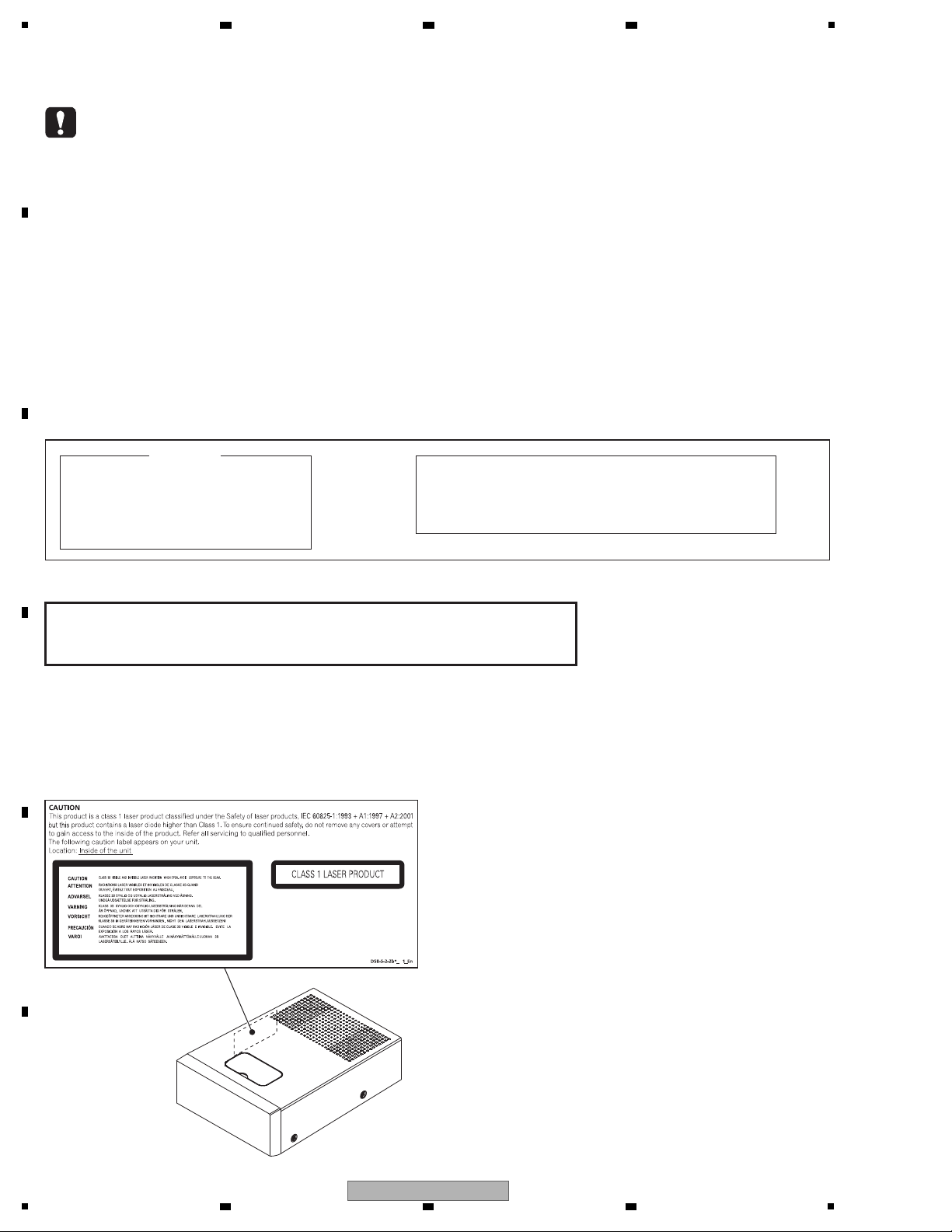
LABEL CHECK
B
WARNING
The Laser component is capable of emitting radiation exceeding the limit for CLASS 1.
A specially instructed person should do servicing operation of the apparatus.
2 3 4
SAFETY INFORMATION
A
B
C
D
E
F
2
1
2 3 4
X-HM20-K
Page 3

5
6 7 8
CONTENTS
SAFETY INFORMATION.......................................................................................................................................................... 2
1. SERVICE PRECAUTIONS ....................................................................................................................................................4
1.1 NOTES ON SOLDERING............................................................................................................................................... 4
1.2 WHEN REPLACING CD MECHA UNIT.......................................................................................................................... 4
2. SPECIFICATIONS .................................................................................................................................................................5
3. BASIC ITEMS FOR SERVICE ..............................................................................................................................................6
3.1 PCB LOCATIONS ........................................................................................................................................................... 6
3.2 JIGS LIST .......................................................................................................................................................................7
4. BLOCK DIAGRAM ................................................................................................................................................................8
4.1 OVERALL WIRING DIAGRAM .......................................................................................................................................8
4.2 OVERALL BLOCK DIAGRAM....................................................................................................................................... 10
5. DIAGNOSIS ........................................................................................................................................................................ 11
5.1 TROUBLESHOOTING.................................................................................................................................................. 11
5.2 PROTECTION CIRCUIT............................................................................................................................................... 12
6. SERVICE MODE................................................................................................................................................................. 12
7. DISASSEMBLY ................................................................................................................................................................... 13
8. EACH SETTING AND ADJUSTMENT................................................................................................................................ 19
8.1 UPDATING OF THE FIRMWARE ................................................................................................................................. 19
9. EXPLODED VIEWS AND PARTS LIST...............................................................................................................................20
9.1 PACKING SECTION ..................................................................................................................................................... 20
9.2 EXTERIOR SECTION .................................................................................................................................................. 22
10. SCHEMATIC DIAGRAM .................................................................................................................................................... 24
10.1 MAIN PCB ASSY (1/7) ...............................................................................................................................................24
10.2 MAIN PCB ASSY (2/7) ...............................................................................................................................................26
10.3 MAIN PCB ASSY (3/7) ...............................................................................................................................................28
AIN PCB ASSY (4/7) ...............................................................................................................................................30
10.4 M
10.5 MAIN PCB ASSY (5/7) ...............................................................................................................................................32
10.6 MAIN PCB ASSY (6/7) ...............................................................................................................................................34
10.7 MAIN PCB ASSY (7/7) ...............................................................................................................................................36
10.8 iPOD PCB ASSY (X-HM20 ONLY) ............................................................................................................................. 38
10.9 RADIO PCB ASSY ..................................................................................................................................................... 40
10.10 DISPLAY PCB ASSY ................................................................................................................................................42
10.11 KEY-SWITCH PCB ASSY.........................................................................................................................................44
10.12 HEADPHONE PCB ASSY ........................................................................................................................................45
10.13 POWER PCB ASSY ................................................................................................................................................. 46
10.14 USB PCB ASSY ....................................................................................................................................................... 48
11. PCB CONNECTION DIAGRAM........................................................................................................................................50
11.1 MAIN and iPOD PCB ASSYS....................................................................................................
11.2 DISPLAY and KEY-SWITCH PCB ASSYS .................................................................................................................54
11.3 RADIO PCB ASSY ..................................................................................................................................................... 56
11.4 HEADPHONE and USB PCB ASSYS ........................................................................................................................ 57
11.5 POWER PCB ASSY ................................................................................................................................................... 58
.................................50
A
B
C
D
E
F
X-HM20-K
5
6 7 8
3
Page 4
1
• For environmental protection, lead-free solder is used on the printed circuit boards mounted in this unit.
Be sure to use lead-free solder and a soldering iron that can meet specifications for use with lead-free solders for repairs
accompanied by reworking of soldering.
• Compared with conventional eutectic solders, lead-free solders have higher melting points, by approximately 40 ºC.
Therefore, for lead-free soldering, the tip temperature of a soldering iron must be set to around 373 ºC in general, although
the temperature depends on the heat capacity of the PC board on which reworking is required and the weight of the tip of
the soldering iron.
Do NOT use a soldering iron whose tip temperature cannot be controlled.
Compared with eutectic solders, lead-free solders have higher bond strengths but slower wetting times and higher melting
temperatures (hard to melt/easy to harden).
The following lead-free solders are available as service parts:
• Parts numbers of lead-free solder:
GYP1006 1.0 in dia.
GYP1007 0.6 in dia.
GYP1008 0.3 in dia.
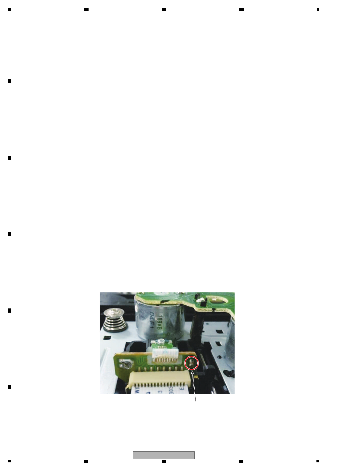
It is necessary to remove the soldering on the short circuit point after connecting the flexible cable.
Short circuit point
2 3 4
1. SERVICE PRECAUTIONS
1.1 NOTES ON SOLDERING
A
B
C
1.2 WHEN REPLACING CD MECHA UNIT
D
E
F
4
1
2 3 4
X-HM20-K
Page 5
5
iPhone adapters x3
(X-HM20 only)
(92L43200033101)
(92L43200033201)
(92L43200033301)
FM aerial
(92L28101510501)
Remote control
(92L34900101001)
“AA” size battery
Accessories
AM loop aerial
(92L50100680101)
Power Cord
(92L20018200101)
Warranty card
Operation instructions
(92L87500200101)
As part of ou r policy of continuous improvement,
PIONEER reserves the right to make design and
specification changes for product improvement without
prior notice. The performance specification figures
indicated are nominal values of production units. There
may be some deviations from these values in individual
units.
g General
Power source AC 220 V to 240 V, 50 Hz/60 Hz
Power
consumption
Power on:
45 W (X-HM20)
30 W (X-HM10)
Power stand-by: 0.4 W
Dimensions Width: 215 mm
Height: 99 mm
Depth: 300 mm
Weight 3.8 kg (X-HM20)
3.7 kg (X-HM10)
g Amplifier
Output power RMS: 15 W + 15 W (1 kHz, 10 %
T.H.D., 4 ohms)
Output terminals Speakers: 4 ohms
20 Hz to 20 kHz
Video output (X-HM20 only): 1 Vp-p
Headphones: 16 ohms
(recommended: 32 ohms)
Input terminals Line in (Analog input):
500 mV/47 k ohms
g CD player
Type Single disc multi-play compact disc
player
Signal readout Non-contact, 3-beam
semiconductor laser pickup
D/A converter Multi bit D/A converter
Frequency
response
20 Hz to 20 000 Hz
Dynamic range 90 dB (1 kHz)
g USB
USB host interface k Complies with USB 1.1 (Full
Speed)/2.0 Mass Storage
Class.
k Support Bulk only and CBI
protocol.
Support file k MPEG 1 Layer 3
k WMA (Non DRM)
Bitrate support k MP3 (32 kbps to 320 kbps)
k WMA (64 kbps to 160 kbps)
Other k Maximum total number of
MP3/WMA files is 999.
k Maximum total number of
folders is 99 INCLUSIVE of
root directory.
k The ID3TAG information
supported are TITLE, ARTIST
and ALBUM only.
k Supports ID3TAG version 1
and version 2.
File system
support
k Support USB devices with
Microsoft Windows/DOS/FAT
12/FAT 16/ FAT 32.
k 2 kbyte block length for sector.
g Tuner
Frequency range FM: 87.5 MHz to 108 MHz
AM: 522 kHz to 1,620 kHz
Preset 40 (FM and AM station)
g Speaker
X-HM20
Type 2-way type speaker system
5 cm Tweeter
10 cm Woofer
Maximum input
power
15 W
Impedance 4 ohms
Dimensions Width: 132 mm
Height: 260 mm
Depth: 173 mm
Weight 2.0 kg/each
X-HM10
Type 2-way type speaker system
Piezoelectric Tweeter
10 cm Woofer
Maximum input
power
15 W
Impedance 4 ohms
Dimensions Width: 132 mm
Height: 260 mm
Depth: 158 mm
Weight 1.6 kg/each
2. SPECIFICATIONS
6 7 8
A
B
C
D
5
X-HM20-K
6 7 8
E
F
5
Page 6
1
A
MAIN
PCB ASSY
H
USB
PCB ASSY
LOADER
ASSY
CD MECHA UNIT
Bottom view
Bottom view
B
iPOD PCB ASSY
(X-HM20 ONLY )
G
POWER PCB ASSY
C
RADIO PCB ASSY
F
HEADPHONE
PCB ASSY
D
DISPLAY
PCB ASSY
E
KEY-SWITCH
PCB ASSY
1..MAIN PCB ASSY (X-HM20) 92L36100201011
1..MAIN PCB ASSY (X-HM10) 92L36100101011
> 1..POWER PCB ASSY (X-HM20) 92L36800201010
> 1..POWER PCB ASSY (X-HM10) 92L36800101010
1..DISPLAY PCB ASSY (X-HM20) 92L36500201010
1..DISPLAY PCB ASSY (X-HM10) 92L36500101010
1..RADIO PCB ASSY (X-HM20) 92L36400201010
1..RADIO PCB ASSY (X-HM10) 92L36400101010
1..HEADPHONE PCB ASSY (X-HM20) 92L37100201011
1..HEADPHONE PCB ASSY (X-HM10) 92L37100101011
1..USB PCB ASSY (X-HM20) 92L36900201011
1..USB PCB ASSY (X-HM10) 92L36900101011
1..iPOD PCB ASSY (X-HM20 ONLY) 92L36600201010
1..KEY-SWITCH PCB ASSY (X-HM20) 92L37200201010
1..KEY-SWITCH PCB ASSY (X-HM10) 92L37200101011
1..CD MECHA UNIT 92L28700220301
1..LOADER ASSY 92L5150020071T
Mark No. Description Part No. Mark No. Description Part No.
LIST OF ASSEMBLIES
NOTES: - Parts marked by “NSP” are generally unavailable because they are not in our Master Spare Parts List.
-
The > mark found on some component parts indicates the importance of the safety factor of the part.
Therefore, when replacing, be sure to use parts of identical designation.
2 3 4
3. BASIC ITEMS FOR SERVICE
3.1 PCB LOCATIONS
A
B
C
D
E
F
6
1
2 3 4
X-HM20-K
Page 7
5
Lubricants and Glues List
Name Part No. Remarks
Adhesive (No. 1600B) GYL1007 Refer to "7. DISASSEMBLY".
6 7 8
3.2 JIGS LIST
A
B
C
D
E
F
X-HM20-K
5
6 7 8
7
Page 8
1
A
MAIN PCB ASSY
(X-HM20: 92L36100
(X-HM10: 92L36100
E
KE
(X
(X
C
RADIO PCB ASSY
(X-HM20: 92L36400201010)
(X-HM10: 92L36400101010)
F
HEADPHONE PCB ASSY
(X-HM20: 92L37100201011)
(X-HM10: 92L37100101011)
H
USB PCB ASSY
(X-HM20: 92L36900201011)
(X-HM10: 92L36900101011)
A
1/7-A7/7
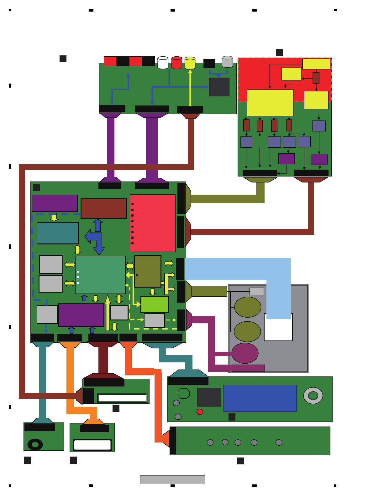
4. BLOCK DIAGRAM
4.1 OVERALL WIRING DIAGRAM
A
B
2 3 4
C
D
E
F
8
1
X-HM20-K
2 3 4
Page 9
5
B
iPOD PCB ASSY
(92L36600201010)
D
DISPLAY PCB ASSY
(X-HM20: 92L36500201010)
(X-HM10: 92L36500101010)
E
KEY-SWITCH PCB ASSY
(X-HM20: 92L37200201010)
(X-HM10: 92L37200101011)
A
7/7
-
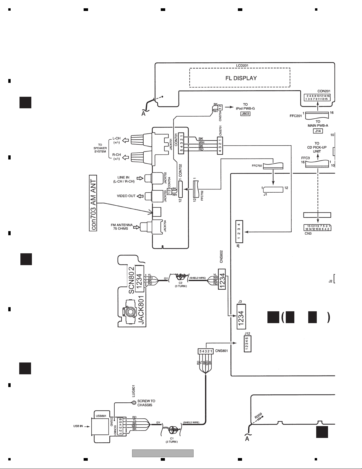
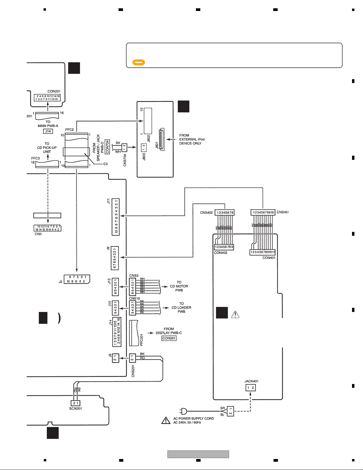
When ordering service parts, be sure to refer to "EXPLODED VIEWS and PARTS LIST" or "PCB PARTS LIST".
-
The > mark found on some component parts indicates the impor tance of the safety factor of the part.
Therefore, when replacing, be sure to use parts of identical designation.
-
: The power supply is shown with the marked box.
(X-HM20 ONLY)
G
POWER PCB ASSY
(X-HM20: 92L36800201010)
(X-HM10: 92L36800101010)
6 7 8
A
B
C
D
E
F
X-HM20-K
5
6 7 8
9
Page 10
1
PLAY STOP UP DOWN OPEN/CLOSE
D407
~D410
D411
~D414
D415
~D418
KBU802
CON 401 (11P)
CON 402 (9P)
REG.8V
IC402
REG.5V
IC401
D419
~D421
AC INLET
RELAY
(RL401)
MAIN TRANS.
SUB.
TRANS
T401
D401
~D404
F401
F402
F403
F404
PRIMARY
SECTION
J14 (16P)
J11 (10P)
J9 (8P)
TUNER
Si4730
IC701
CON702 (12P)
(CON703)
(JACK701)
(JACK702)
(JACK704)
(JACK703)
IR
FL DISPLAY LCD201
CON 201 (16P)
FL
DRIVER
( IC 201)
VOLUME VR
(VOL201)
KEY BUTTON
IC 1
OPTEK OTK 5256
Microprocessor
Audio DSP
Audio Decoder
U5
Philip
SAA7824HL
SERVO DSP
U8
AUDIO_CODEC
WM8781
U900
POWER AMP IC
STA 339BW/S
IC 7
FLASH_IC
8M
U7
DRIVER_IC
SA1469
U2
MULTIPLEXER
PI5V331W
IC902
SDRAM
1Mx16bit
IC901
iPod
certification
U3
MULTIPLEXER
FSUSB30MUX
DOCK CONNECTOR
J802 (10P)
J2 (10P)
J12(5P)
J3(4P)
USB CONNECTOR
SCN801(6P)
SCN802(4P)
LOADING
MOTOR
SLIDE
MOTOR
SPIN
MOTOR
PICK UP
J10 (5P)
J13 (6P)
CN3(16P)
J1 (12P)
Power Supply
8V (Motor Supply)
iPod 5V [U501]
USB 5V [U551]
AMP IC 18V
VDD 3.3V [IC8]
VDD1.8V [U4]
OTHER 3.3V [IC6]
FL (F1, F2, VP- )
CON701(4P)
J6 (4P)
Video OutAUX INSPK Terminal Jack
AM Cone FM Coaxial
CON704(2P)
PU in
Open /Close SW
SCN201(2P)
J5(2P)
J803
(2P)
HP
(JACK801)
F405
FUNCTION
POWER ON
LED
IC13
HP AMP
TDA1308
IC800
SA6208
A
MAIN PCB ASSY
F
HEADPHONE
PCB ASSY
H
USB PCB ASSY
E
KEY-SWITCH PCB ASSY
LOADER ASSY
D
DISPLAY PCB ASSY
B
iPOD PCB
ASSY
(X-HM20 ONLY )
C
RADIO PCB
ASSY
G
POWER PCB ASSY
2 3 4
4.2 OVERALL BLOCK DIAGRAM
A
B
C
D
E
F
10
1
X-HM20-K
2 3 4
Page 11
1. Does the pickup move to the PICKUP-IN Switch
position?
Check Sled circuit. U7 (pin 17,18,19,20)
Although a CD is inserted and the Tray is closed, "NO DISC" is displayed.
Press the Tray CD Eject Button without inserting a disc, and try starting the playback operation.
Yes
No
2. Does the focus (lens) move up and down?
Check Focus peripheral circuit.
U5 (pin 65) U7 (pin 1 to 4)
No
Yes
3. Is the laser lit?
Check the laser diode at U5 pin 80 and R128
peripheral circuit.
No
Yes
4. Is the turntable rotating?
Check Spindle circuit.
U5 (pin 68), U7 (pin 9,10,11,12)
No
Yes
5. Is the Laser power, Focus, Tracking circuit OK?
Check the Laser power, Focus, Tracking peripheral
circuit. U5 (pin 64, 65, 80), U7 (pin 1 to 4 24 to 27)
No
Ye s
Ye s
Check the IC401, D401 to D404, T401, F405
(POWER PCB Assy). At abnormal, replace
POWER PCB Assy.
No
No Power
Is the voltage of MCU+5V
(POWER PCB Assy CON402-1 pin)
5 V?
Check the IC8, U4 (MAIN PCB Assy).
At abnormal, replace MAIN PCB Assy.
No
Check the RELAY_CTL line.
No
Is the VDD3.3V (MAIN PCB Assy
IC8-3 pin), VDD1.8V (MAIN PCB Assy
U4-5 pin) output?
Ye s
Ye s
Check the F401 to F404 power lines.
At abnormal, replace POWER PCB Assy.
Replace MAIN PCB Assy.
No
Does the voltages output in CON401?
(POWER PCB Assy: +B: 18V, USB_VCC: 12V,
iPod_VCC: 12V, +8V)
After having pressed STANDBY/ON
button, is the voltage of RELAY_CTL
(POWER PCB Assy CON402-3 pin) 3.3V
and is RELAY (RL401) on?
5
5. DIAGNOSIS
5.1 TROUBLESHOOTING
6 7 8
A
B
C
D
E
F
X-HM20-K
5
6 7 8
11
Page 12

1
The protection circuit is activated when a failure in power or voltage is generated in the D-AMP circuit. If the protection circuit is
activated, the unit will shut itself off and the TIMER indicator on the front panel will start flashing. The indicator will continue to
flash until the problem is resolved. After a shutdown, to turn the unit back on, unplug the AC power cord then plug it back into
the AC outlet.
5.2 PROTECTION CIRCUIT
A
B
6. SERVICE MODE
There is no information to be shown in this chapter.
2 3 4
C
D
E
F
12
1
2 3 4
X-HM20-K
Page 13
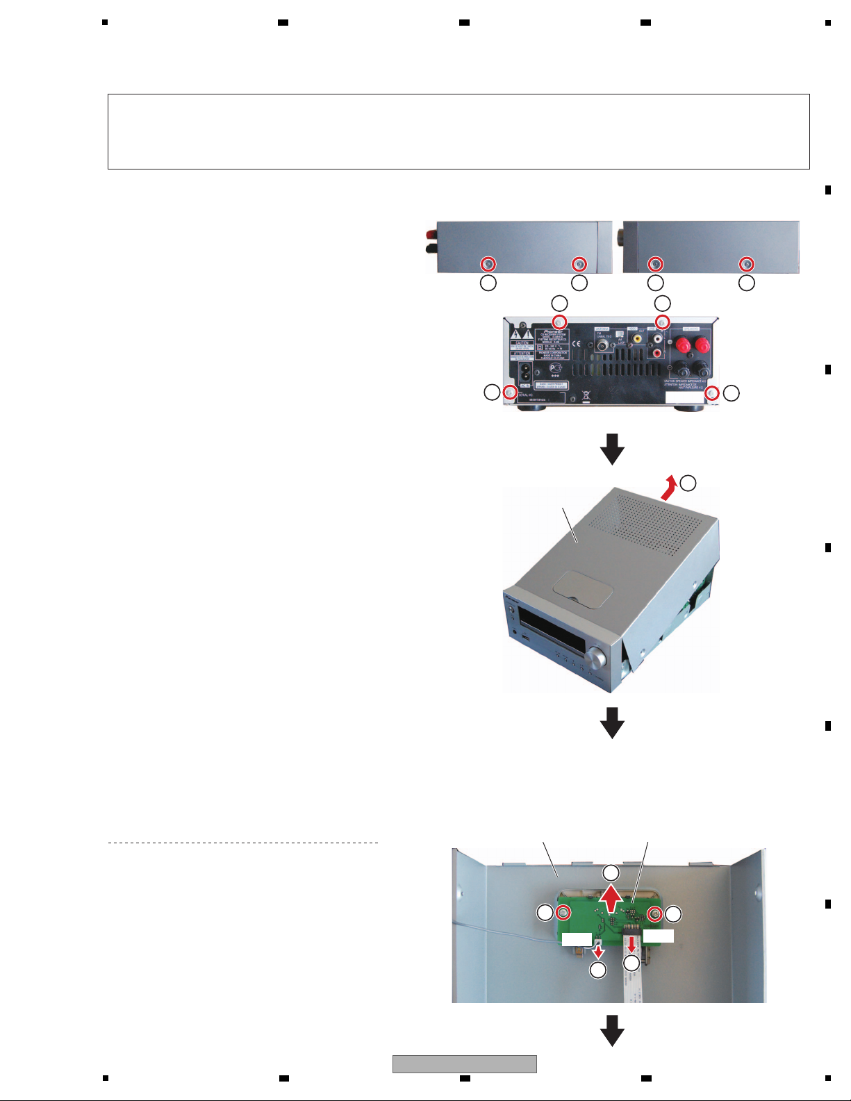
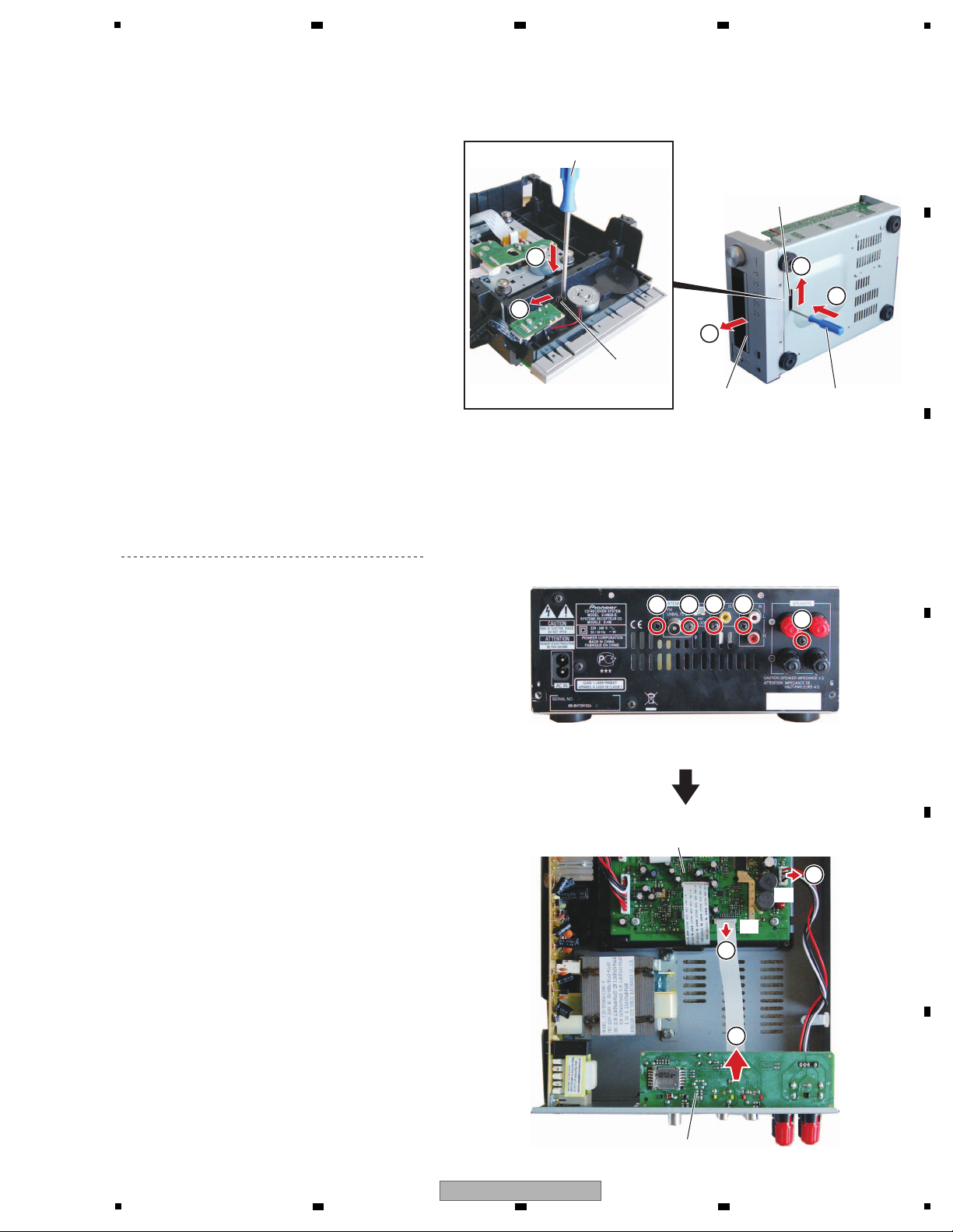
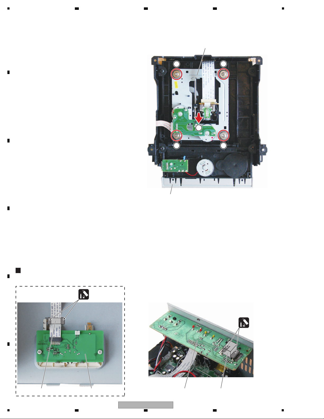
5
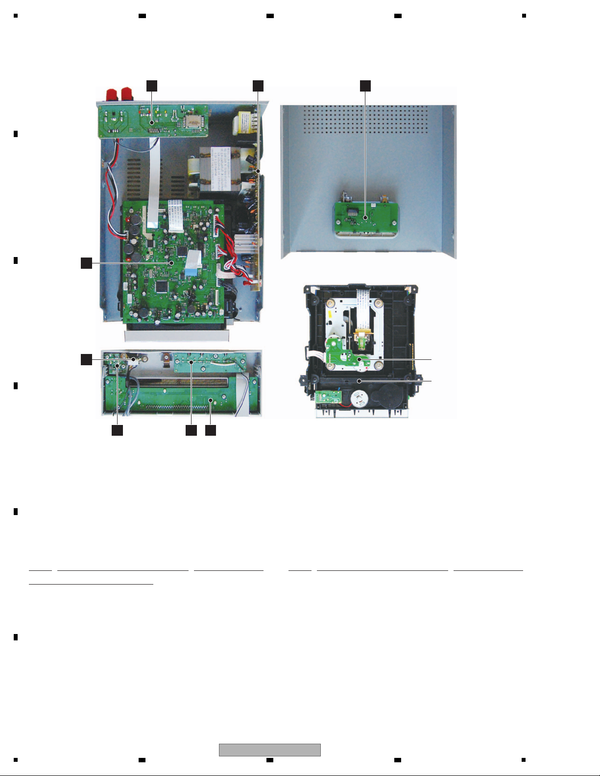
(1) Remove the four screws.
(2) Remove the four screws.
[1] Top Cabinet
Note:
(1) Do NOT look directly into the pickup lens. The laser beam may cause eye injury.
(2) Even if the unit shown in the photos and illustrations in this manual may differ from your product, the
procedures described here are common.
3
1
2 2
2
2
2
2
1 1 1
(3) Remove the top cabinet.
Note (X-HM20 only):
Please do not damage the cables when removing
the top cabinet.
(1) Disconnect the one flexible cable and one
connectors. (J802, J803)
(2) Remove the two screws.
(3) Remove the iPOD PCB Assy.
Top cabinet
Top cabinet iPOD PCB Assy
• Rear view
1
1
[2] iPOD PCB Assy (X-HM20 only)
• Bottom view
J803
J802
(1) Remove the top cabinet.
(See procedure "[1] Top Cabinet".)
3
6 7 8
7. DISASSEMBLY
A
B
C
D
5
X-HM20-K
6 7 8
E
F
13
Page 14
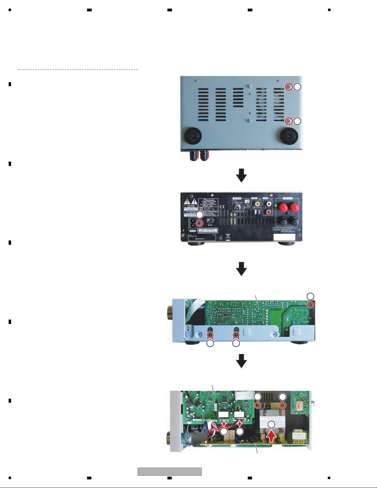
1
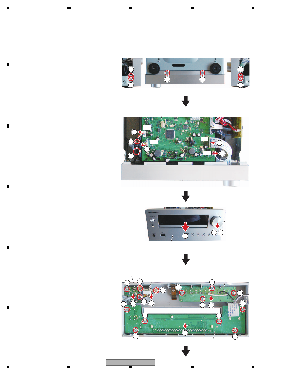
(1) Remove the two screws.
(2) Remove the two screws.
(3) Unhook the two hooks.
[3] Front Panel Section
(1) Remove the top cabinet.
(See procedure "[1] Top Cabinet".)
(4) Disconnect the one flexible cable and three
connectors. (J3, J5, J12, J14)
(5) Release the jumper wires from hook.
(6) Remove the one screw.
(7) Remove the volume knob.
(8) Remove the nut and washers.
(9) Remove the front panel section.
(10) Remove the two screws.
(11) Remove the 12 screws.
(12) Remove the DISPLAY, KEY-SWITCH,
HEADPHONE and USB PCB Assemblies.
9
1 1
22
3 3
Front panel section
DISPLAY PCB Assy
KEY-SWITCH PCB Assy
USB PCB Assy
HEADPHONE PCB Assy
Volume knob
• Bottom view
7 8
6
10
10
11
11
11
11
11
11
11
11
12
12
12
12
11
11
11
11
MAIN PCB Assy
4
J14
J5
J3
J12
4
4
4
5
A
B
2 3 4
C
D
E
F
14
1
X-HM20-K
2 3 4
Page 15
5
• Bottom view
2
2
3
1
1
Thin minus screwdriver
Thin minus screwdriver
Slit
Tr ay
Lever
(1) Insert the thin minus screwdriver to the slit.
(2) Slide the lever in the arrow direction.
(3) Pull out the tray by hand.
How to open the tary when the power cannot be on
(1) Remove the five screws.
(2) Disconnect the one flexible cable and one
connectors. (J1, J6)
(3) Remove the RADIO PCB Assy.
[4] RADIO PCB Assy
(1) Remove the top cabinet.
(See procedure "[1] Top Cabinet".)
1
11
11
RADIO PCB Assy
MAIN PCB Assy
• Rear view
2
2
J1
J6
3
6 7 8
A
B
C
D
5
X-HM20-K
6 7 8
E
F
15
Page 16
1
(1) Remove the two screws.
(2) Remove the one screw.
(3) Remove the three screws.
(4) Remove the two screws.
(5) Disconnect the two connectors.
(J9, J11)
(6) Remove the POWER PCB Assy.
[5] POWER PCB Assy
(1) Remove the top cabinet.
(See procedure "[1] Top Cabinet".)
1
1
• Bottom view
2
3
4
4
33
• Rear view
POWER PCB Assy
POWER PCB Assy
MAIN PCB Assy
5
J11J9
6
5
A
B
2 3 4
C
D
E
F
16
1
X-HM20-K
2 3 4
Page 17
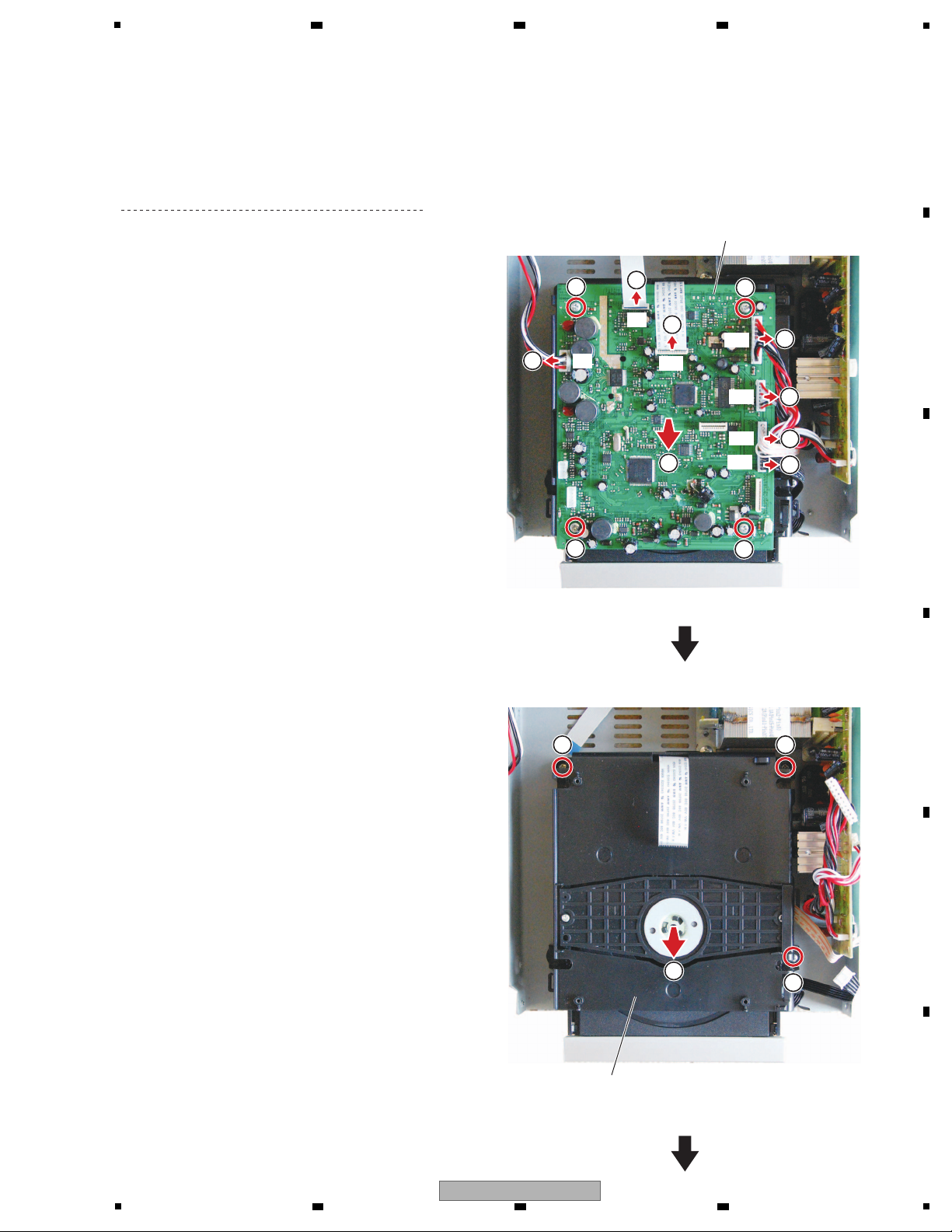
5
(1) Disconnect the two flexible cables and five
connectors. (J1, J6, J9, J10, J11, J13, J19)
(2) Remove the four screws.
(3) Remove the MAIN PCB Assy.
(4) Remove the three screws.
(5) Remove the LOADER Assy.
[6] MAIN PCB Assy, LOADER Assy, CD MECHA Unit
(1) Remove the top cabinet.
(See procedure "[1] Top Cabinet".)
(2) Remove the front panel section.
(See procedure "[3] Front Panel Section".)
2
2
2
2
4 4
4
MAIN PCB Assy
LOADER Assy
1
1
1
3
5
1
1
1
1
J11
J13
J10
J19
J9
J1
J6
6 7 8
A
B
C
D
E
X-HM20-K
5
6 7 8
F
17
Page 18
1
(6) Remove the four screws.
(7) Remove the CD MECHA Unit.
6
6
66
CD MECHA Unit
7
• Bottom view
Note:
Removal of the disc tray cover is not required
during disassembly/reassembly of the front panel
section, because this cover does not interfere with
the front panel.
Disc tray cover
RADIO PCB Assy
Gasket
iPOD PCB Assy
X-HM20 ONLY
Ferrite core
The Application Position of Adhesive
Adhesive (No.1600B)
GYL1007
Adhesive (No.1600B)
GYL1007
A
B
2 3 4
C
D
E
F
18
X-HM20-K
1
2 3 4
Page 19

5
MCU software
1. Create a "system" folder in USB device.
Note: "system" folder must be written in lower-case letter.
2. Copy the upgrade file (upgrade_Pioneer_108P.bin) and the text file (upgrade.txt) into the "system" folder in USB device.
3. Turn on the main unit and select the USB function.
4. Connect the USB device.
5. FL will display "Upgrade" - indicating upgrading in process.
Caution: During upgrading process, DO NOT CUT THE AC SUPPLY.
6. FL will display "Success" - indicating the upgrading process is completed.
7. After FL display "Success", unplug the power cord from the main unit then only remove the USB device from main unit.
8. Re-plug in the power cord to the main unit and turn on the main unit.
The software upgrade is completed.
To check the software version
1. Press INPUT button to "Line in" function.
2. In "Line in" function,
short press np button once then long press f(PLAY/PAUSE) button until the software version is displayed.
software version display: X-HM20-K/-S → "CD-HM20R Vxxx", X-HM10-K/-S → "CD-HM10R Vxxx"
6 7 8
8. EACH SETTING AND ADJUSTMENT
8.1 UPDATING OF THE FIRMWARE
A
B
C
D
E
F
X-HM20-K
5
6 7 8
19
Page 20
1
NOTES: - Parts marked by “NSP” are generally unavailable because they are not in our Master Spare Parts List.
-
The > mark found on some component parts indicates the importance of the safety factor of the part.
Therefore, when replacing, be sure to use parts of identical designation.
-
Screws adjacent to b mark on product are used for disassembly.
-
For the applying amount of lubricants or glue, follow the instructions in this manual.
(In the case of no amount instructions, apply as you think it appropriate.)
X-HM20
only
2 3 4
9. EXPLODED VIEWS AND PARTS LIST
A
9.1 PACKING SECTION
B
C
D
E
F
20
1
2 3 4
X-HM20-K
Page 21
5
6 7 8
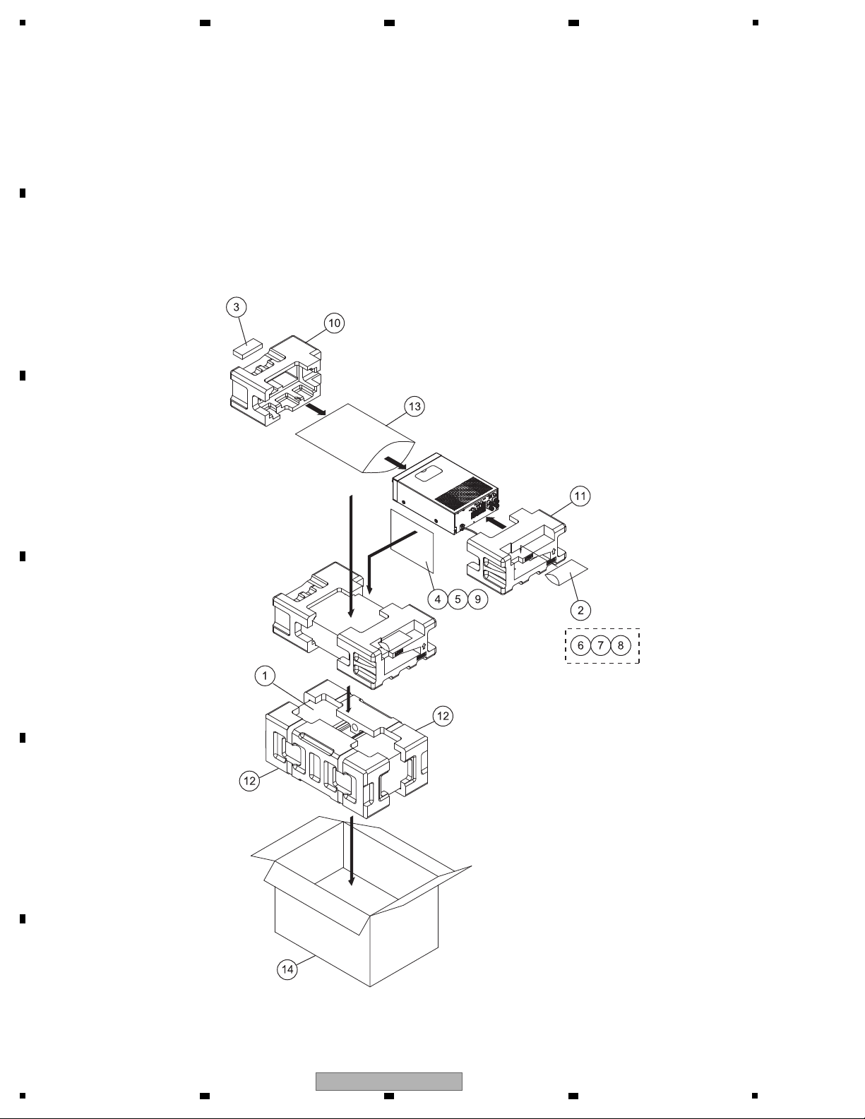
(1) PACKING SECTION PARTS LIST
Mark No. Description Part No.
1 Speaker See Contrast table (2)
> 2Power Cord 92L20018200101
3 Remote Control 92L34900101001
4 AM Loop Aerial 92L50100680101
5 FM Aerial 92L28101510501
6 iPhone Adaptor See Contrast table (2)
7 iPhone 3G Adaptor See Contrast table (2)
8 iPhone 4G Adaptor See Contrast table (2)
9 Operating Instructions 92L87500200101
(En, Fr, Es, De, It, Nl, Ru)
A
10 Front Packing Add 92L87000200101
11 Rear Packing Add 92L87000200201
12 Speaker Packing Add See Contrast table (2)
13 Miramat Bag Unit 92L89134045001
14 Packing Case See Contrast table (2)
(2) CONTRAST TABLE
X-HM20-K/SYXJC8, X-HM20-S/SYXJC8, X-HM10-K/SYXJC8 and X-HM10-S/SYXJC8 are constructed the same except for the
following:
Mark No. Symbol and Description
1 Speaker 92L33400201001 92L33400201001 92L33400101002 92L33400101002
6 iPhone Adaptor 92L43200033101 92L43200033101 Not used Not used
7 iPhone 3G Adaptor 92L43200033201 92L43200033201 Not used Not used
8 iPhone 4G Adaptor 92L43200033301 92L43200033301 Not used Not used
12 Speaker Packing Add 92L87000200301 92L87000200301 92L87001510201 92L87001510201
14 Packing Case 92L89600200102 92L89600200101 92L89600104102 92L89600104101
X-HM20-K
/SYXJC8
X-HM20-S
/SYXJC8
X-HM10-K
/SYXJC8
X-HM10-S
/SYXJC8
B
C
D
E
F
X-HM20-K
5
6 7 8
21
Page 22

1
A
C
D
E
G
H
F
B
X-HM20-K,
X-HM20-S
only
9.2 EXTERIOR SECTION
A
B
2 3 4
C
D
E
F
22
1
2 3 4
X-HM20-K
Page 23

5
6 7 8
(1) EXTERIOR SECTION PARTS LIST
Mark
No. Description Part No.
1 MAIN PCB Assy See Contrast table (2)
> 2POWER PCB Assy See Contrast table (2)
3 DISPLAY PCB Assy See Contrast table (2)
4 RADIO PCB Assy See Contrast table (2)
5 HEADPHONE PCB Assy See Contrast table (2)
No. Description Part No.
Mark
26 Door Washer See Contrast table (2)
27 Main Chassis 92L54500200101
28 Rear Panel See Contrast table (2)
29 PWB Bracket 92L72900200101
30 Spring Plate See Contrast table (2)
A
6 USB PCB Assy See Contrast table (2)
7 iPOD PCB Assy See Contrast table (2)
8 KEY-SWITCH PCB Assy See Contrast table (2)
9 • • • • •
10 CD MECHA Unit 92L28700220301
11 LOADER Assy 92L5150020071T
12 Front Cabinet Assy See Contrast table (2)
13 Power Button Assy See Contrast table (2)
14 Operation Button See Contrast table (2)
15 Volume Knob See Contrast table (2)
16 iPod Door See Contrast table (2)
17 iPod Holder See Contrast table (2)
18 Top Cabinet See Contrast table (2)
19 Disc Tray Cover See Contrast table (2)
20 ESD Sheet 92L45900200101
21 iPod Door Cushion See Contrast table (2)
22 Leg 92L48301510201
23 FL Holder 92L51500200101
24 iPod Spacer See Contrast table (2)
25 CD Mecha Holder 92L51501510101
31 Laser Label 92L88900200201
32 Leg Cushion 92L48300200101
33 • • • • •
34 Washer 92L65004000101
35 Washer 92L65004000201
36 Screw BBZ30P080FTC
37 Scre
w BB
Z30P100FTC
38 Screw 2.6x6 92L75526906001
39 Screw 2.6x8 92L75526908001
40 Screw 3.0x6 92L75603006001
41 Screw 3.0x6 92L75603006002
42 Screw 3.0x8 92L75603008001
43 Screw 4.0x8 92L75604008001
44 Screw 92L77017906001
45 Screw 2.6x8 92L78026908002
46 Screw 3.0x6 See Contrast table (2)
47 Screw 3.0x8 See Contrast table (2)
B
C
(2) CONTRAST TABLE
X-HM20-K/SYXJC8, X-HM20-S/SYXJC8, X-HM10-K/SYXJC8 and X-HM10-S/SYXJC8 are constructed the same except for the following:
Mark No. Symbol and Description
1 MAIN PCB Assy 92L36100201011 92L36100201011 92L36100101011 92L36100101011
> 2POWER PCB Assy 92L36800201010 92L36800201010 92L36800101010 92L36800101010
3 DISPLAY PCB Assy 92L36500201010 92L36500201010 92L36500101010 92L36500101010
4 RADIO PCB Assy 92L36400201010 92L36400201010 92L36400101010 92L36400101010
5 HEADPHONE PCB Assy 92L37100201011 92L37100201011 92L37100101011 92L37100101011
6 USB PCB Assy 92L36900201011 92L36900201011 92L36900101011 92L36900101011
7 iPOD PCB Assy 92L36600201010 92L36600201010 Not used Not used
8KEY-SWITCH PCB Assy 92L37200201010 92L37200201010 92L37200101011 92L37200101011
12 Front Cabinet Assy 92L20100200102 92L20100200101 92L20100100102 92L20100100101
13 Power Button Assy 92L20700200102 92L20700200101 92L20700200102 92L20700200101
14 Operation Button 92L20800200102 92L20800200101 92L20800200102 92L20800200101
15 Volume Knob 92L20900300102 92L20900200102 92L20900300102 92L20900200102
16 iPod Door 92L40300200102 92L40300200101 Not used Not used
17 iPod Holder 92L40300200202 92L40300200201 Not used Not used
18 Top Cabinet 92L43100200103 92L43100200101 92L43100100201 92L43100100101
19 Disc Tray Cover 92L43800200102 92L43800200101 92L43800200102 92L43800200101
21 iPod Door Cushion 92L48300200501 92L48300200401 Not used Not used
24 iPod Spacer 92L51500200201 92L51500200201 Not used Not used
26 Door Washer 92L51501510501 92L51501510501 Not used Not used
28 Rear Panel 92L70200200102 92L70200200101 92L70200100102 92L70200100101
30 Spring Plate 92L73000200101 92L73000200101 Not used Not used
46 Screw 3.0x6 92L75603006002 92L75603006001 92L75603006002 92L75603006001
47 Screw 3.0x8 92L76503008013 92L76503008012 92L76503008013 92L76503008012
X-HM20-K
/SYXJC8
X-HM20-S
/SYXJC8
X-HM10-K
/SYXJC8
X-HM10-S
/SYXJC8
D
E
F
X-HM20-K
5
6 7 8
23
Page 24

1
VDD_3v3 1.5mA at 32KHz
1.8v LDO 250uA(output)500uA(input) at 32KHz with SD_clk 32KHz output
A18
A17
A15
USB_ID H for slave mode,L for Host mode
delay 180ms
1,0.22uF 16ms
2,1uF 56ms
2.
1.
Y1
24MHz
Y2
32.768KHz
C27
22pF
C28
22pF
C29
20pF
C30
20pF
R19
1M
R20
10K+_1%
C3
104P
C4
104P
C7
104P
C5
104P
C9
104P
C15
104P
C16
104P
C18
104P
C33
104P
C34
1uF
C35
104P
C36
104P
C37
104P
C38
104P
R22
100R
1
PDVDD
2
S(D)RAM_WE/GPIO1[15]
25
A0/GPIO1[17]
24
A1/GPIO1[18]
23
A2/GPIO1[19]
22
A3/GPIO1[20]
3
A4/GPIO1[21]
4
A5/GPIO1[22]
34
GPIO1[0]/UART_TX
35
GPIO1[1]/UART_RX
38
GPIO1[2]/SPI_CLK
36
GPIO1[3]/SPI_MOSI
13
PDVSS
14
PDVDD
40
GPIO1[4]/SPI_MISO
39
GPIO1[5]/SPI_CS048GPIO1[6]/SPI_CS1
5
A6/GPIO1[23]
6
A7/GPIO1[24]
20
PVDD_1V8
7
A8/GPIO1[25]
8
A9/GPIO1[26]
27
A10/GPIO1[27]
17
A11/GPIO1[28]
18
A12/GPIO1[29]
26
PDVDD
29
A13/SDRAM_BANK0/GPIO1[30]
28
A14/SDRAM_BANK1/GPIO1[31]
33
A15/LDQM/IO2[0]
21
A16/SDRAM_UDQM/GPIO2[1]
32
A17/SDRAM_CAS/GPIO2[2]
31
A18/SDRAM_RAS/GPIO2[3]
GPIO0[30]/
GPIO0[29
125
GPIO0[28]/I2S_1_DIN
GPIO0[27
GPIO0[26
124
GPIO0[25]/CD_CFLG
GP
GPIO0[23
GPIO0[2
GPIO0[2
GPIO0[20
GP
GPIO0[1
GPIO0
GPIO0
GPIO0
GPIO0
GPIO
GPIO
GPIO
GPIO
GP
GP
GP
GP
GP
GP
GPIO
61
GPIO0[2]/LCD_DEN
GPIO0
104
USB_ID
103
USB_VBUS
102
VDDA_USB_1V8
101
USB_RES10K_1%_REF
100
VCCA_USB_3V3
99
USB_DM98USB_DP
97
AGND
105
ADC_CH_0
106
ADC_CH_1
107
ADC_CH_2
108
AVDD_PLL_3V3
109
AVSS_PLL
110
PVDD_1V8
111
GPIO0[31]/PWM_OUT
112
T_MODE
113
RESET
114
JTRST
115
JTMS/TX_1
116
JTCK/RX_1
117
JTDI/TORARY_A
118
JTDO/ROTARY_B
119
PDVDD
120
PI32KHZ
121
PO32KHZ
122
PI24MHZ
123
PO24MHZ
127
GPIO1[9]
126
GPIO1[10]
128
PVSS
GPIO0
64
D15/GPIO2[19]
62
PDVDD63D14/GPIO2[18]
60
D13/GPIO2[17]
59
D12/GPIO2[16]
58
D11/GPIO2[15]
57
D10/GPIO2[14]
56
D9/GPIO2[13]
49
PVDD_1V8
55
D8/GPIO2[12]
54
SRAM_OE/GPIO1[16]
53
SRAM_CS/GPIO1[14]
30
SDRAM_CS/GPIO1[13]
19
SDRAM_CLK
50
PDVDD52SDRAM_CLKE/GPIO1[11]
41
D7/GPIO2[11]
42
D6/GPIO2[10]
43
D5/GPIO2[9]
44
D4/GPIO2[8]45D3/GPIO2[7]
46
D2/GPIO2[6]
47
D1/GPIO2[5]
16
A24/SPI_DATA3
15
A23/SPI_DATA2
10
A22/SPI_DATA1
37
PDVDD
9
A21/SPI_DATA0
12
A20/SPI_CLK
11
A19/SPI_CS
51
D0/GPIO2[4]
IC1
OPTEK_OTK5256
R82
5M
R55
10K
T1
T4
R127
220R
Q1 3906
R16
4
R27
150K
R32
39K
R49
100K
Q4
3904
Q9
3906
R50
10K
R51
39K
R58
4K7
R140
NA
R141
0R
C78
NA
C80
NA
C81
NA
C82
NA
C10
10uF
C139
10pF
C77
1nF
FB5
NC
FB7
121
VDD_3V3
VDD_3V3
VDD_3V3
VDD_1V8
VDD_3V3
VDD_1V8
VDD_3V3
VDD_1V8
RESET
JTRST
JTMS
JTCK
JTDI
JTDO
VDD_3V3
A13
A0
A1
A10
A2
A3
SD_UDQM
A4
A5
A6
A7
A8
A9
D0
D10
D11
D12
D13
D2
D3D4D5D6D7
D8
D9
SDRAM_CS
SD_CAS
SD_RAS
SPI_FLASH_CLK
SPI_FLASH_D0
SPI_FLASH_D1
SPI_FLASH_D2
SPI_FLASH_D3
SPI_FLASH_CS
D1
R/W
UART_TX
UART_RX
SD_LDQM
SD_CLKE
SD_CLK
AMP_RESET
VDD_3V3
VDD_1V8
VDD_3V3
USB_D-
USB_D+
V
KEY0
+3V3
RESET
SPI_CLK
SPI_CS0
SPI_MOSI
USB_POW_CTL
SHORT_DET
KEY1
KEY2
VFD_RESET
SE_CFLG/DVD_TRIN
ADC_DAT
A
GPIO_SDA
GPIO_SCL
IPOD_POW_CTL
+3V3
LOW_VOLTAGE_DET
USB5.1V
A
1/7
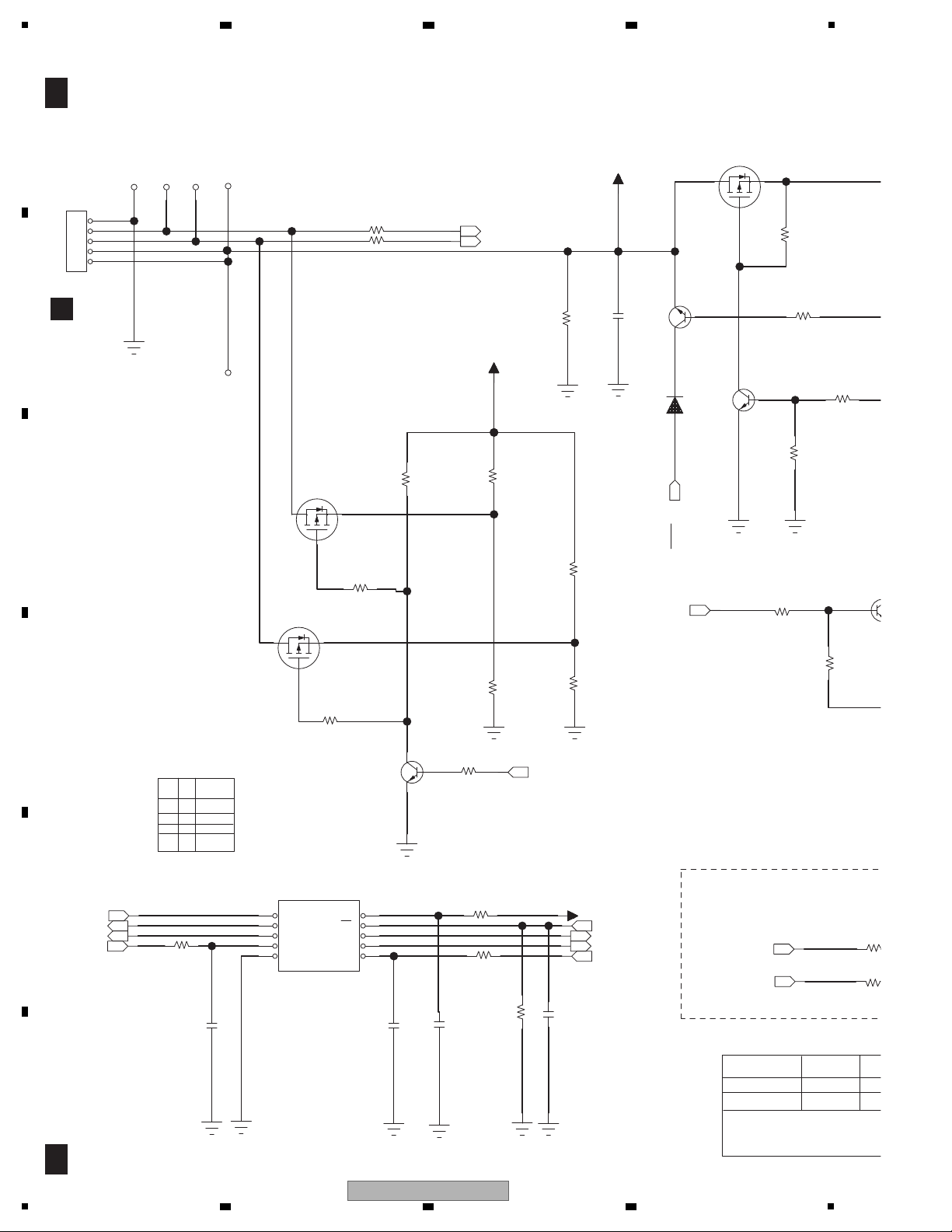
MAIN PCB ASSY
(X-HM20: 92L36100201011)
(X-HM10: 92L36100101011)
A
1/7
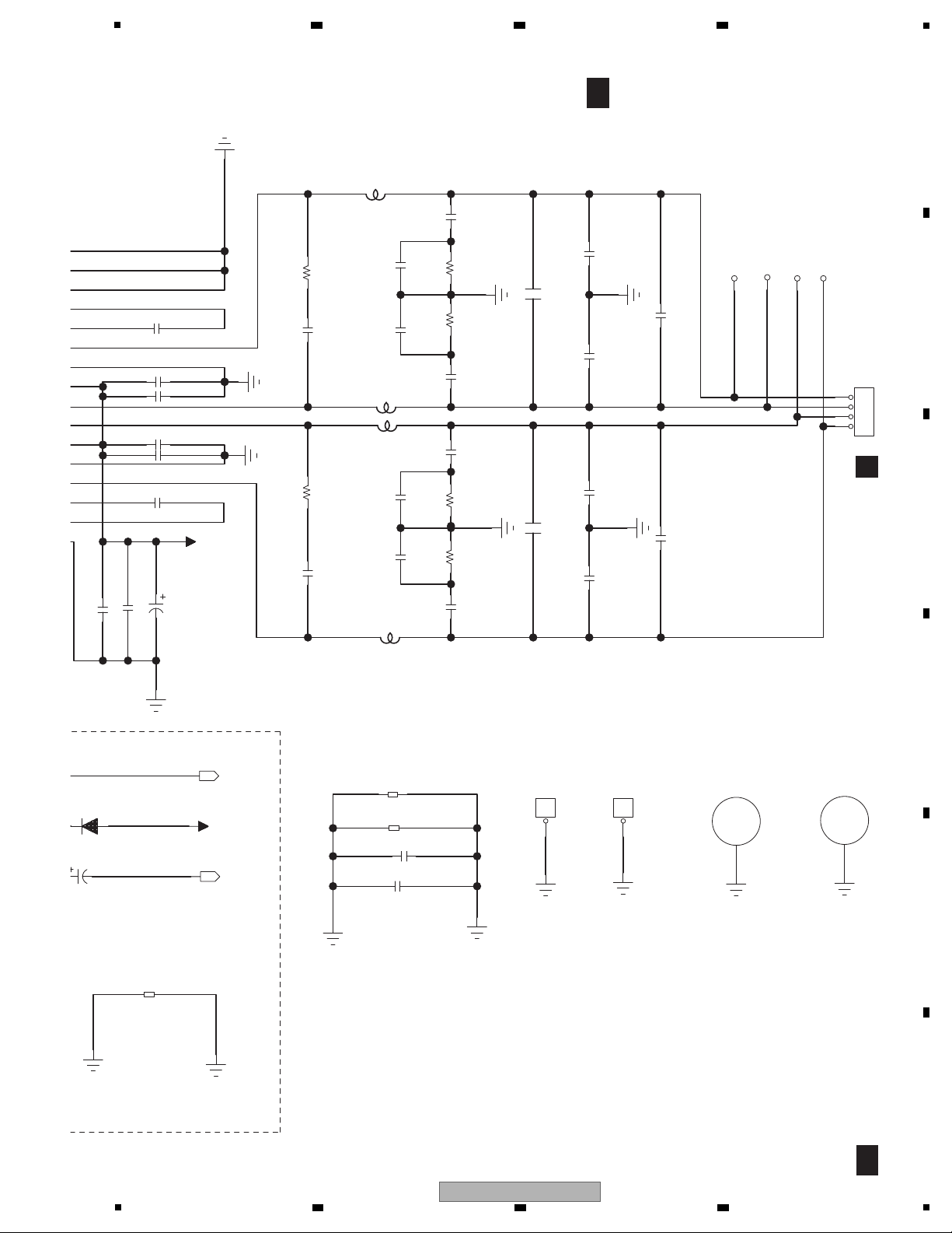
10. SCHEMATIC DIAGRAM
10.1 MAIN PCB ASSY (1/7)
A
B
2 3 4
C
D
E
F
24
1
X-HM20-K
2 3 4
Page 25

Following Points is necessary for software tools online debug connection
2th Funciton for iPod_POW_CTL
L for USB_3v3 of 5256 On
for Standby_LED_CTL
for Buck H Enable
for analog_channel_SEL
For setting version
Notes:In DVD mode R66 don't populate.R130 will be changed to 10R
R20
10K+_1%
R599
NA
R597
10K
R594
10K
R595
10K
C18
104P
C31
104P
C32
104P
C33
104P
C34
1uF
C35
104P
R171
15K
1
CS
2
DO(IO1)
3
WP(IO2)
4
GND
8
VCC
7
HOLD(IO3)
6
CLK
5
DI(IO0)
IC7
W25Q80BVSSI
C50
104P
96
GPIO0[30]/I2S_MCLK_I/O
95
GPIO0[29]/I2S_1_DOUT
94
GPIO0[27]/I2S_1_LRCK
93
GPIO0[26]/I2S_1_BCLK
92
GPIO0[24]/CD_EF
88
GPIO0[23]/I2S_0_DOUT
91
GPIO0[22]/I2S_0_DIN
90
GPIO0[21]/I2S_0_LRCK
89
GPIO0[20]/I2S_0_BCLK
85
PDVDD
76
GPIO0[19]/SD_WP
80
GPIO0[18]/SD_DETECT
82
GPIO0[17]/SD_DATA3
84
GPIO0[16]/SD_DATA2
77
GPIO0[15]/SD_DATA1
78
GPIO0[14]/SD_DATA0
81
GPIO0[13]/SD_CMD
79
GPIO0[12]/SD_CLK
83
PVDD_1V8
72
GPIO0[11]/LCD_D7
71
GPIO0[10]/LCD_D6
70
GPIO0[9]/LCD_D5
69
GPIO0[8]/LCD_D4
68
GPIO0[7]/LCD_D3
67
GPIO0[6]/LCD_D2
66
GPIO0[5]/LCD_D1
65
GPIO0[4]/LCD_D0
75
GPIO0[3]/DOT_CLK
61
GPIO0[2]/LCD_DEN
73
GPIO0[1]/LCD_VSYNC
USB_ID
103
USB_VBUS
102
VDDA_USB_1V8
101
USB_RES10K_1%_REF
100
VCCA_USB_3V3
99
USB_DM98USB_DP
97
AGND
87
GPIO1[7]/SDA
86
GPIO1[8]/SCL
74
GPIO0[0]/LCD_HSYNC
64
D15/GPIO2[19]
62
PDVDD63D14/GPIO2[18]
60
D13/GPIO2[17]
59
D12/GPIO2[16]
D11/GPIO2[15]
R52
15K
R55
10K
R130
910R
FB1
121
R108
100R
R109
470R
R122
100R
R127
220R
T5
T9
T10
T11
T12
T13
T2
Q1 3906
R16
4K7
R6
15K
R7
NA
FB9
121
R3
100R
R17
100R
R64
47R
R66
1K1
C62
10pF
R121
15K
C14
1uF
R123
15K
R119
X-HM20: 10K
X-HM10: 39K
C139
10pF
FB5
NC
VDD_3V3
LCD_D0
LCD_D1
LCD_D2
VDD_1V8
AMP_STD
CLOSE_DET
VDD_3V3
DAC_BCLK
DAC_LRCK
DAC_DATA
LCD_D0
LCD_D1
VDD_3V3
LCD_D2
+3V3
KEY0
SPI_FLASH_CS
SPI_FLASH_D2
SPI_FLASH_D3
SPI_FLASH_CLK
SPI_FLASH_D0
D11
D12
D13
D14
D15
SPI_FLASH_D1
SE_RESET
HW_SDA
HW_SCL
VDD_3V3
VDD_1V8
USB_D-
USB_D+
MCU_+5V
SE_CLK
+3V3
IRDA
+3V3
JTDI
JTDO
JTCK
JTMS
JTRST
+3V3
LCD_D4
STANDBY _KEY
TUNER_RE SET/DAB _1V2_CTL
RELAY_CTL
IPOD_SEL
CD/DVD_ON
OPEN_DET
TRAY_IN
KEY1
KEY2
SE_EF/CVBS_IPOD
SE_DATA
SE_LRCK
SE_BCLK
ROTARY_A
ROTARY_B
AUDIO_CLK
CLASS_D_CLK
DVD_USB_SEL
LCD_D4
EARPHON E_IN_DE T
+3V3
IPOD_DET
ACC_POWER
VDD_3V3
TRAY_OUT
ANALOG_CH_SEL
KEY1
A
1/7
5
6 7 8
A
B
C
D
E
5
6 7 8
X-HM20-K
F
25
Page 26

1
BANK0
Only for software Debug
must be delayed to 100ms when present 3v3
Note:don't populate
1,In the Tuner:R111,R112,R10,R88
2,In the DAB mode:R101,R103,R104,R8
1
VDD1
2
IO0
3
IO1
4
VSSQ1
5
IO2
6
IO3
7
VDDQ1
8
IO4
9
IO5
10
VSSQ2
11
IO6
12
IO7
13
VDDQ2
14
LDQM
15
WE
16
CAS
17
RAS
18
CS
19
A11
20
A10/AP
21
A0
22
A1
23
A2
24
A3
25
VDD2
26
VSS1
27
A4
28
A5
29
A6
30
A7
31
A8
32
A9
33
NC
34
CKE
35
CLK
36
UDQM
37
NC/RFU
38
VDDQ3
39
IO8
40
IO9
41
VSSQ3
42
IO10
43
IO11
44
VDDQ4
45
IO12
46
IO13
47
VSSQ4
48
IO14
49
IO15
50
VSS2
IC902
1Mx 16bit SDRAM
FB991
121
C991
100uF
C992
104P
C993
104P
C994
104P
C995
104P
C996
104P
C997
104P
C998
104P
R863
1K
C853
104P
Q851
3904
R862
100K
C854100uF
FB17
121
FB24
NC
FB25
121
FB32
121
FB33
121
R65
100R
R101
100R
R103
100R
R104
100R
FB34
121
FB35
NC
FB36
121
R111
NA/100R
R112
NA/100R
12
11
10
9
8
7
6
5
4
3
2
1
J1
CON12_S
R8
100R
Q850
SS855
R10
NA/15K
R88
NA/15K
T119
T120
T121
T122-
T123
T124
T125
T126
T127
T128
T129
T130
]31:0[A]51:0[D
A0
A1
A2
A3
A4
A5
A6
A7
A8
A9
A10
A13
SD_LDQM
R/W
SD_CAS
SD_RAS
SDRAM_CS
SD_CLKE
SD_CLK
SD_UDQM
D0
D1
D2
D3
D4
D5
D6
D7
D8
D9
D10
D11
D12
D13
D14
D15
+3V3
TUNER_RESET/DAB_1V2_C TL
TUNER/DAB_3V3
TUNER/DAB_3V3
TUNER_RESET/DAB_1V2_CTL
GPIO_SCL
GPIO_SDA
RDS_DAVN
UART_TX
UART_RX
REAR_RCA_IN_R
REAR_RCA_IN_L
TUNER/DAB_L
TUNER/DAB_R
+3V3
RADIO_GND
RCA_GND
VDD_SDRAM
A
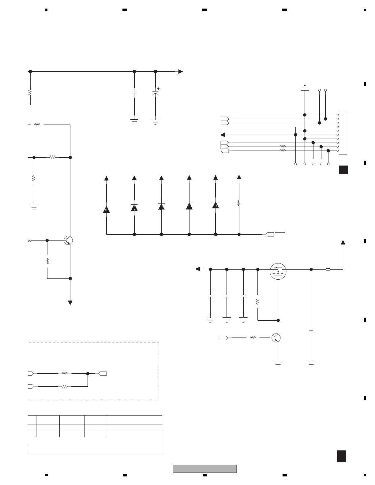
2/7
MAIN PCB ASSY
(X-HM20: 92L36100201011)
(X-HM10: 92L36100101011)
A
2/7
C
CON702
10.2 MAIN PCB ASSY (2/7)
A
2 3 4
B
C
D
E
F
26
1
X-HM20-K
2 3 4
Page 27

5
Hold Low for at least 30ms
For iPod certification
X-HM20 ONLY
For Tray Loder controll
C910
104P
1
NC
2
MODE1/SPICS
3
NC
4
RESET
5
VCC
15
NC
14
MODE0/CLK
13
SDA/SOMI
12
SCL/SIMO
11
VSS
16NC17NC18NC19NC20
NC
10
NC9NC8NC7NC6NC
IC901
IPOD_PHONE_CP
R910
10K
R43
100
R44
100
R60
15K
R61
15K
C70
1nF
1
2
3
4
5
J10
CON5_S
T8
T14
T17
T18
T19
R62
10R
1
VCC
2
BOUT
3
GND
4
AOUT
8
AIN
7
GND
6
NC
5
BIN
IC800
SA6208
FB27
0R
C43
104P
C852
104P
R863
1K
C853
104P
Q851
3904
R862
100K
R864
4K7
FB853
121
Q850
SS8550
OTHER_3V3
GPIO_SCL
GPIO_SDA
TUNER_RESET/DAB_1V2_CTL
OPEN_DET
CLOSE_DET
OTHER_3V3
LD+
LD-
LD-
LD+
A_+5V6
TRAY_OUT
TRAY_IN
OTHER_3V3
ANALOG_CH_SEL
VDD_SDRAM
A
2/7
LOADER ASSY
6 7 8
A
B
C
D
E
5
X-HM20-K
6 7 8
F
27
Page 28

1
Optional
for CD
for iPod
for iPad/USB
for Amp
PGND
MOTO_GND
1.22v
1.22v
only for DVD model
only for 75mA
Only for DVD model
C504
104P
L501
C512
10nF
R
R505
12K
D501
S240
R503
15K
LL4148
D701
LL4148
C702
104P
C502
5.6nF
C501
104P
7
EN
8
SS
3
SW
5
FB
1
BS
2
IN
6
COMP
4
GND
9
SHIELD
U501
MP1482
C553
104P
C561
10nF
D551
S340
R553
15K
D554
LL4148
C559
104P
C552
5.6nF
C551
104P
7
EN
8
SS
3
SW
5
FB
1
BS
2
IN
6
COMP
4
GND
9 SHIELD
U551
MP1430
10
9
8
7
6
5
4
3
2
1
J11
CON10_S
Pitch 2.5
FB31
0R
C67
104P
FB19
2A
FB20
2A
FB21
2A
FB37
2A
C21
104P
D3
LL4148
T21
T22
T23
T24
T25
T26
T49
T65
T66
T67
T68
T69
T70
T71
C53
104P
C24
104P
R131
470R
C60
104P
R132
NA
T72
T73
C39
104P
C40
104P
3
VIN2VOUT
1
GND
IC2
1117/5V
C75
470uF
C23
10uF
8
7
6
5
4
3
2
1
J9
CON8_S
C26
104P
R76
1K
Q12
NC
R169
47K
R158
100K
C505 220uF/25v
C554 220uF/25v
R137
1R5
R139
1R5
C20
100uF/25v
C701
220uF/25v
C560
100uF/25v
D601
PMEG2101EA
C601 470uF
Q601
MMBT 3906
Q60
R601
1K
R603
1K
C209220uF
T15
R602
15K
R1
NC
R2
0R
R78
22K
R81
22K
R84
22K
R96
22K
D15
LL4148
+12V_0.7A
12V/0.7A
18V/4.5A
12V/1.1A
12V/0.7A
7.5V/1.5A
+12V_1A1
12V/1.1A
-VP
VF1
VF2
MCU_+5V
DGND
DGND-1
DGND
BUCK_EN
BUCK_EN
A_+5V6
CD/DVD_ON
LOW_VOLTAGE_DET
V7_OTOM V7_OTOM
+3V3
RELAY_CTL
A_+5V6
MOTO_7V
MCU_+5V
DGND-1
+3V3
A
3/7
MAIN PCB ASSY
(X-HM20: 92L36100201011)
(X-HM10: 92L36100101011)
A
3/7
G
CON401
G
CON402
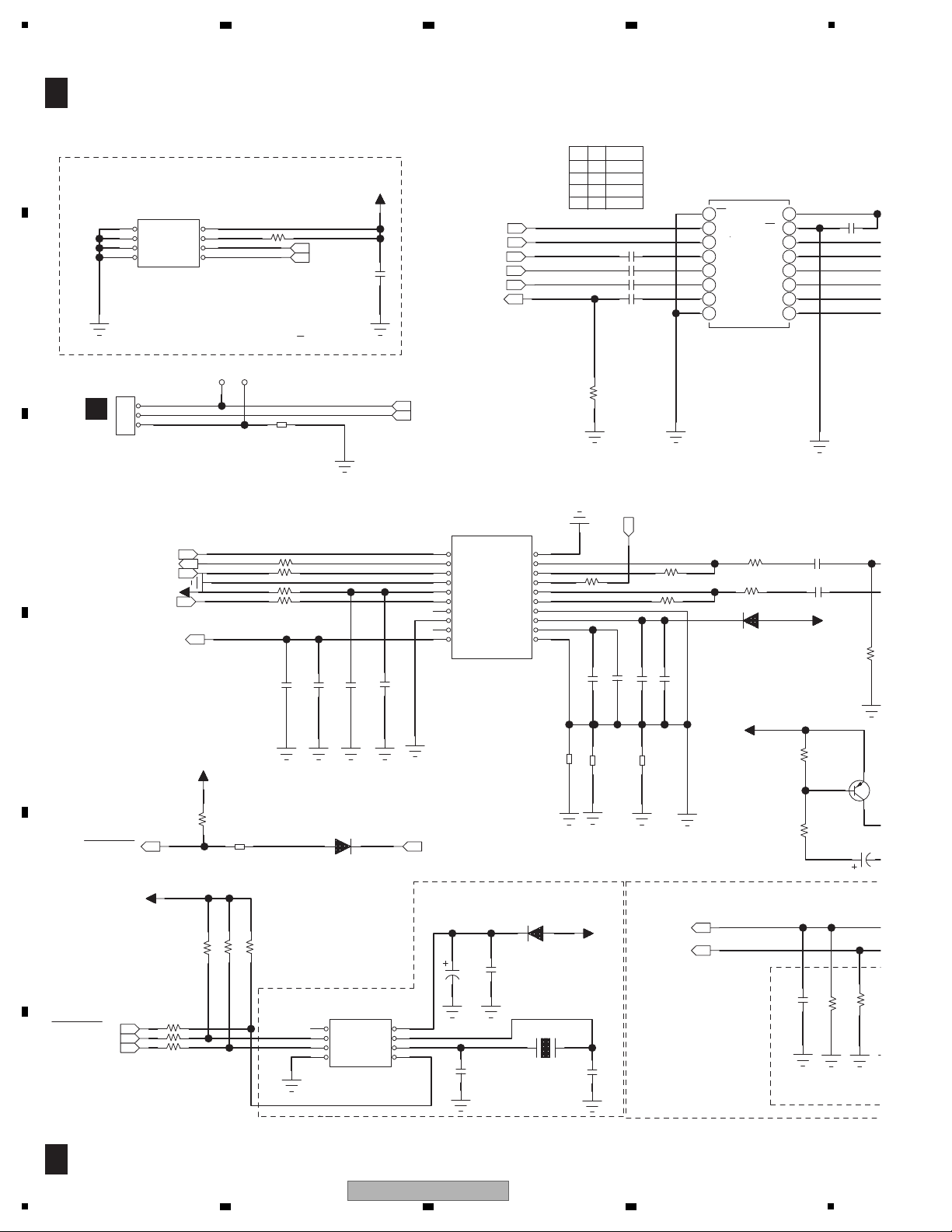
10.3 MAIN PCB ASSY (3/7)
A
B
C
2 3 4
D
E
F
28
X-HM20-K
1
2 3 4
Page 29

5
LC1207CC3TR33
Optional
Optional
1.22v
1.22v
C227
104P
C228
104P
C229
1uF
C231 220uF
1
VIN
3
STBY
5
VOUT
4
NC
2
GND
U4
AP2121-1.8V
FB6
121
R4
10K
C42
104P
FB8
121
C44
104P
2
VIN3VOUT
1
GND
IC8
C1
104P
C41
10uF
C88 220uF
C79
10uF
FB12
121
C84
104P
C86 220uF
L501
15uH/3A
C512
10nF
C507
104P
C508
10uF
R504
56K
R505
12K
D501
S240
D503
LL4148
3
5
L502
15uH/4A
C561
10nF
C556
104P
C557
10uF
R554
39K
R555
12K
D551
S340
R553
15K
D552
LL4148
C552
5.6nF
3
SW
5
FB
1
BS
6
COMP
MP1430
C97
104P
C98
104P
C100
104P
C101 220uF
3
VIN2VOUT
1
GND
IC6
AMS1117
C102 220uF
D2
PMEG2010EA
C53
104P
C24
104P
C54
4.7uF
D13
NA/PMEG2101EA
FB2
121
C555
470uF
C506 470uF
A
C601 470uF
MMBT 3906
Q602
S8050
Q603
S8050
R603
1K
R604
4R7
R605
2R2
D509
SS14
R602
15K
C6
470uF
C8
104P
C13 470uF
C51
104P
+3V3
+3V3
1V8
VDD_1V8
VDD_3V3
MCU_+5V
IPOD_5.1V
USB_5.1V
OTHER_3V3
A_+5V6
+3V3
1V8
1V8
+3V3
USB5.1V
A
3/7
6 7 8
A
B
C
D
E
5
X-HM20-K
6 7 8
F
29
Page 30
1
S1 S0 channels
L L 0
L H 1
H L 2
H H 3
IPOD_SEL
DVD_USB_SEL
PIN/FUNCTION DVD_USB AU
L
H
L
L
Note:IPOD_SEL=USB_HW_CHARGE
DVD_USB_SEL=IPOD_HW_CHANGE
iPad_HW_CHARGE by USB port
R846
0R
R847
0R
C820
104P
R810
2R2
C847
104P
1
2
3
Q5 AP2301GN
R67
43.2K
R68
49.9K
R69
75.0K
R70
49.9K
1
2
3
Q6 AP2301GN
R71
10K
R72
10K
Q7
3904
R73
4K7
R110
2R2
R113
2R2
C63
10pF
C64
10pF
R46
10K
R114
10K
1
2
3
4
5
J12
CON5_S
R25
10K
T74
T75
T76
T77T78
1
2
3
Q15
PMV65XP
Q17
R159
100K
R160
1K
Q18
3904
R161
100K
R162
4K7
R163
10K
Q420
3904
R497
1K
1
S/L=1
2
HSD1+
3
HSD2+
4
D+
5
GND
6
D-
7
HSD2-
8
HSD1-
9
OE
10
VCC
U3
SGM7222/FSUSB30MUX
D5
LL4148
C142
102P
R115
R117
USB_PORT_D-
USB_PORT_D+
USB_D-
USB_D+
OTHER_3V3
USB_VBUS
USB_VBUS
IPOD_SEL
USB_POW_CTL
IPOD_SEL
IPOD_D+
IPOD_D-
DVD_USB_SEL
USB_PORT_D+
USB_PORT_D-
SHORT_DET
DVD_USB_SEL
LCD_D2
A
4/7
MAIN PCB ASSY
(X-HM20: 92L36100201011)
(X-HM10: 92L36100101011)
A
4/7
H
SCN801
10.4 MAIN PCB ASSY (4/7)
A
B
C
D
2 3 4
E
F
30
1
X-HM20-K
2 3 4
Page 31
5
iPod docking subboard connector
pitch1.25
L
H
L
LLHH
H
DEFAULT
R807
1K
10
9
8
7
6
5
4
3
2
1
J2
CON10_S
R806
1K
FB800
0R
C804
104P
C843 220uF
C844
104P
C68
104P
T20
T50
T51
T52
T53
T54
T55
D8
LL4148
D9
LL4148
D11
LL4148
D10
LL4148
D12
LL4148
R85
4K7
Q16
3904
Q17
MMBT 3906
R159
100K
R160
1K
R161
100K
4K7
R163
10K
Q19
AP2301GN
R164
100K
C806
10uF
C805
10uF
R116
10K
497
1K
R115
0
R117
NC
IPOD_D+
IPOD_D-
IPOD_+5V
IPOD_DET
ACC_POWER
IPOD_POW_CTL
IPOD_5.1V
USB_5.1V
IPOD_HW_CHARNGE_CTL
SHORT_DET
USB_5.1VIPOD_5.1V
OTHER_3V3
A_+5V6
7.5V/1.5A
IPOD_+5V
+3V3
OTHER_3V3
IPOD_HW_CHARNGE_CTL
A
4/7
B
J802
6 7 8
A
B
C
D
E
F
X-HM20-K
5
6 7 8
31
Page 32

1
Class_D_AMP
Headphone circuit section
C933
104P
C9
10
C932
1nF/25v
1
GND_SUB
2
SA
3
TEST_MODE
4
VSS
5
VCC_REG
6
OUT2B
7
GND2
8
VCC2
9
OUT2A
10
OUT1B
11
VCC1
12
GND1
13
OUT1A
14
GND_REG
15
VDD
16
CONFIG
17
OUT3B
18
OUT3A
19
OUT4A
20
OUT4B
21
VDD_DIG
22
VSS_DIG
23
POWER_DN
24
PLL_VDD
25
PLL_FT
26
PLL_GND
27
XT1
28
BICKI
29
LRCKI
30
SDI
31
RESET
32
INT_LINE
33
SDA
34
SCL
35
GND_DIG
36
VCC_DIG
37
U900
STA339BW/S
R901
100R
C901
104P
R902
100R
FB901
121
R903
10K
C904
104P
FB902
121
FB903
121
FB904
121
FB905
121
R905
2K2
C905
680pF
C906
4.7nF
FB906
121
C907
104P
R906
22R
R907
1K
C908
104P
C909
104P
C913
10
C914
C915
1
C916
1
R915
10K
C911
C912
R925
4K7
R926
4K7
C945
470P
R927
4K7
R928
4K7
C946
150P
R930
4K7
R931
4K7
1
OUTA
2
-
3
+
4
VSS
8
VDD
7
OUTB
6
-
5
+
IC13
TDA1308
R932
4K7
R934
4K7
C947
470P
R935
4K7
R936
4K7
C948
150P
R937
4K7
R938
4K7
C949
220pF
R939 4.99K 1%
C950 100uF
C951
220pF
R951 4.99K (1%)
C952 100uF
R953
10K
R954
10K
C953
220pF
R955
10K
R956
10K
C954
220pF
C955
104P
C956100uF
FB912
121
D901
PMEG2101EA
R960
3K3
FB910
8K2
C965
1nF
D14
LL4148
FB920
121
FB921
121
FB922
121
FB923
121
FB924
121
FB925
121
FB257
121
FB911
12
C960
22uF
GPIO_SCL
GPIO_SDA
OTHER_3V3
AMP_RESET
DAC_DATA
DAC_LRCK
DAC_BCLK
CLASS_D_CLK
AMP_3V3
AMP_3V3
AMP_STD
AMP_3V3
I2S_DATA
OUT3A
OUT3B
OUT4A
OUT4B
OUT3B
OUT3A
OUT4B
OUT4A
SHORT_DET
AA_+5V
AA_+5V
AUDIO_IN_AGND
A
5/7
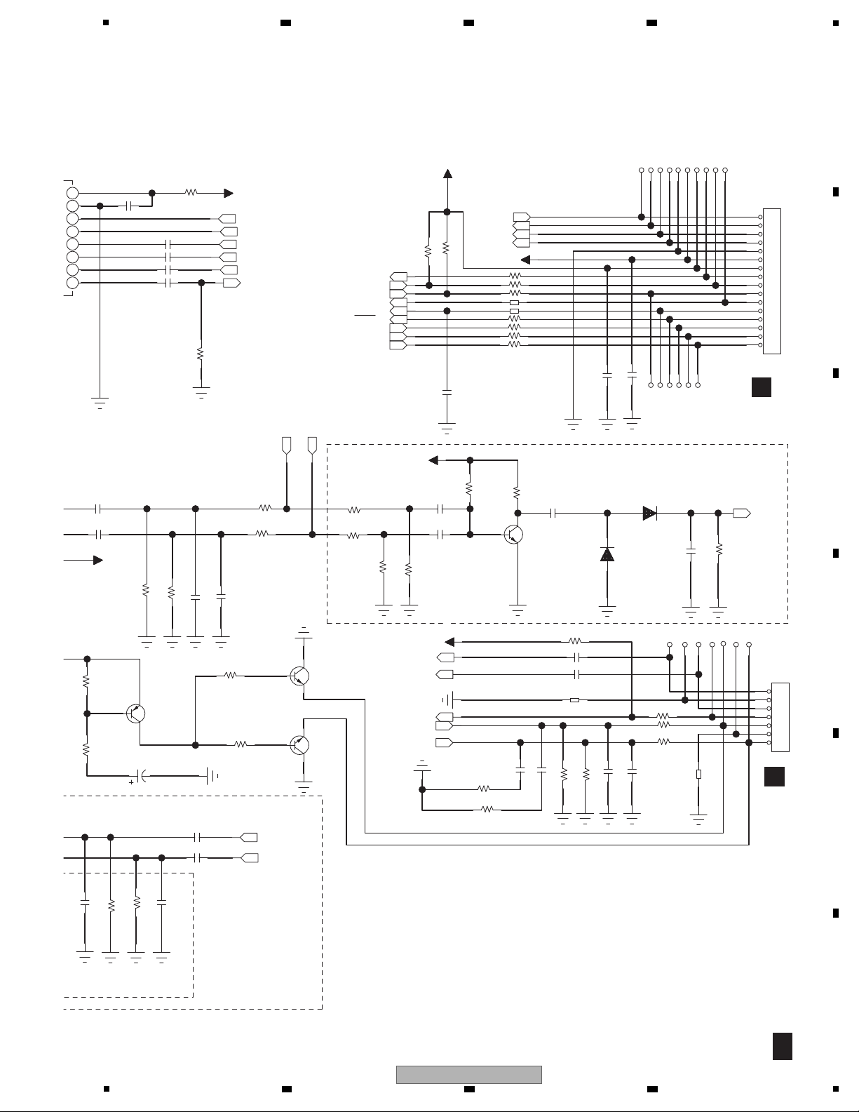
10.5 MAIN PCB ASSY (5/7)
A
2 3 4
B
C
D
1
E
F
32
X-HM20-K
2 3 4
Page 33
5
R+
R-
L+
L-
10uH,1uF,220nF ,2R7 value for 4ohm speak
C933
104P
C931
1000uF/25v
C932
1nF/25v
C913
104P
C914
1uF
C915
104P
C916
1uF
L901
10UH
L902
10UH
L903
10UH
L904
10UH
C927
1uF
C928 1uF
1
2
3
4
J6
CON4_S
T115
T116
T117
T118
C917
330p
R909
20R
C918
330p
R908
20R
R911
4R7
R912
4R7
C919
224
C923
224
C920
224
C922
224
R913
4R7
R914
4R7
C924
224
C942
224
C925
224
C926
224
C929
220nF
C944
220nF
C911
104P
C912
104P
C940
1nF
C941
1nF
C930
1nF
C943
1nF
1
GND
6MM-D-A
100uF
1
GND
6MM-D-A
PMEG2101EA
FB3
NC
FB926
121
1
GND
SOLT-SOLDER
1
GND
SOLT-SOLDER
FB911
121
C141
102P
C143
102P
18V/4.5A
EARPHONE_R
EARPHONE_L
A_+5V6
ADC_AGND
AUDIO_IN_AGND
A
5/7
MAIN PCB ASSY
(X-HM20: 92L36100201011)
(X-HM10: 92L36100101011)
A
5/7
C
CON701
6 7 8
A
B
C
D
E
F
X-HM20-K
5
6 7 8
33
Page 34
1
S1 S0 channels
L L 1
L H 2
H L 3
H H 4
Rear panel board interface
Realtime clock chip
IWL Word Leng
0 =16bit
1=20bit
Z=24bit
FORMAT
Z=I2S
to connect GND of FM/Line/headphone
I2C Adrees:1010 A2 A1 A0 R/w 0xA0
don't populate
don't popula
don't populate
FB11
121
C890
104P
R26
NC
R29
NC
C17
NC
R86
47K
C896
104P
C898
8P
R896
15K
D4
LL4148
1
INTB
2
SCL
3
DAT
4
GND
8
VCC1
7
OSCI
6
OSCO
5
INTA
U895
BL5372
C895
8P
R11
100R
R12
100R
R31
100R
Y3
32.768KHz
FB26
121
R33
4K7
R34
4K7
T63
T64
C83
2.2uF
C89
2.2uF
C90
2.2uF
C
C9
C9
1
ENA
2
IN1
3
S4A
4
S3A
5
S2A
6
S1A
7
DA
8
GND
9
DB
10
S1B
11
S2B
B3S 21
13
S4B
14
IN0
15
ENB
16
VCC
U2
PI5V331W
C9
C96
2.2uF
R125
10K
1
MCLK
2
DOUT
3
LRCLK
4
DGND
5
DVDD
6
BCLK
7
IWL
8
FSAMPEN
9
FORMAT
10
VMID
20
M/S
19
AINL
18
AINOPL
17
COM
16
AINR
15
AINOPR
14
AGND
13
AVDD
12
VREFP
11
VREFGND
U8
WM8781
R142
10R
R144
10R
C99
0.1uF
C103
10uF
C104
0.1uF
C118
10uF
R149
3K3
C121
0.1uF
C130
10uF
C131
0.1uF
C132
10uF
R150
10K
R151
18K
R152
10K
R153
18K
C133
4.7uF
C134
4.7uF
R154
2R2
R155
10R
R156
10K
C897
470uF
Q11
MM
R24
47K
R45
10K
C2 1
D795
IN60
FB795
121
FB796
121
FB797
121
1
A0
2
A1
3
A2
4
GND
8
VCC
7
PCT
6
SCL
5
SDA
IC795
EEPROM
C796
104P
R795
10K
3
2
1
J5
DIP3/2.0mm
D16
LL4148
REAR_RCA_L
REAR_RCA_R
+3V3
+3V3
+3V3
STANDBY_KEY
GPIO_SCL
GPIO_SDA
STANDBY_KEY
KEY0_FRONT
MAX_R
ANALOG_CH_SEL
TUNER/DAB_L
REAR_RCA_L
AUX_FRONT_L
DVD_L_CH
AUDIO_CLK
ADC_DATA
DAC_LRCK
OTHER_3V3
DAC_BCLK
VMID
VMID
A_+5V6
A_+5V6
RADIO_GND
LININ_GND
ADC_AGND
GPIO_SCL_E
GPIO_SDA_E
+3V3
GPIO_SCL_E
GPIO_SDA_E
KEY
KEY0
A
6/7
MAIN PCB ASSY
(X-HM20: 92L36100201011)
(X-HM10: 92L36100101011)
A
6/7
E
SCN201
10.6 MAIN PCB ASSY (6/7)
A
B
C
2 3 4
D
E
F
34
X-HM20-K
1
2 3 4
Page 35
5
Front panel board interface
Standby_LED_CTL
for AUX_DET
don't populate
don't populate
R21
1K
R28
1K
R35
1K
R36
1K
FB10
121
FB13
121
C890
104P
R890
2R2
R54
1K
R56
1K
R57
15K
R59
15K
R63
100R
FB4
121
FB14
121
R13
10K
R14
10K
C11
100pF
C12
100pF
R18
1K
R23
100K
R26
NC
R29
NC
C17
NC
C19
NC
R89
68K
C55
1uF
C57
1uF
Q14
3904
R90
750K
R93
4K7
C58
2.2uF
D6
LL4148
D7
LL4148
R98
15M
16
15
14
13
12
11
10
9
8
7
6
5
4
3
2
1
J14
CON16_S
Pitch1.0
C65
104P
C66
104P
1
2
3
4
5
6
7
J3
7P2.0mm
T56
T57
T58
T59
T60
T61
T62
C46
0R
C47
0R
C48
0R
C49
0R
T79
T80
T81
T82
T83
T84
T85
T86
T87
T88
T89
T90
T91
T92
T93
T94
R75
68K
C92
2.2uF
C93
2.2uF
C94
2.2uF
9
10
11
13
14
15
16
C95
2.2uF
C59
4.7uF
R124
10K
C133
4.7uF
C134
4.7uF
R156
10K
R157
10K
C135
3300pF
C137
3300pF
R170
NA
R172
NA
R173
1K
R174
1K
Q8
3904
Q10
3904
R5
220R
R15
220R
Q11
MMBT 3906
R24
47K
R45
10K
C2 10uF
R47
121
R77
121
R97
47R
R99
47R
C138
22nF
C140
22nF
C795
102P
SPI_CS0
SPI_MOSI
SPI_CLK
VFD_RESET
KEY0
LCD_D1
ROTARY_A
ROTARY_B
OTHER_3V3
IRDA
AUX_FRONT_L
AUX_FRONT_R
EARPHONE_R
EARPHONE_L
EARPHONE_IN_DET
+3V3
OTHER_3V3
KEY2
VF1
VF2
-VP
+3V3
REAR_RCA_IN_L
REAR_RCA_IN_R
KEY0_FRONT
LCD_D0
MAX_L
TUNER/DAB_R
REAR_RCA_R
AUX_FRONT_R
DVD_R_CH
A_+5V6
MAX_L
MAX_R
A_+5V6
AUDIO_IN_AGND
KEY
A
6/7
F
SCN802
D
CON201
6 7 8
A
B
C
D
E
F
X-HM20-K
5
6 7 8
35
Page 36

1
1V7
CD Section
1
LPWR
2
EXTF
3
MONITOR
4
SENSE
5
VSSSA1
6
IREF
7
VDDA1
8
VRFO
9
D1
10
D2
11
D3
12
D4
13
R1
14
R2
15
CEQ
16
VDDA2
17
VSSA2
18
OSCO
19
OSCI
20
VSSA3
60
SBSY
59
SFSY
58
SUB
57
RCK
56
STATUS
55
SILD
54
RAB
53
SCL
52
SDA
51
RESET
50
CLK12
49
CLK16
48
SCLK
47
WCLK
46
DATA
45
EF
44
SCLI
43
WCLI
42
SDI
41
VDDD
61
VSD262DOBM63VDD1
64RA65FO66SL67
MOTO168MOTO2
69
VSD370VDD2
71V172V273V374V475V576
TEST177TEST278TEST379TEST4
80
LASE
40
VSSD39CFLG38CCLK37CDAT36CRDY35RKILL34LKILL33BUGND32BUIL31BUOL30BUOR29BUIR28BUVP27DAVP26DALP25DALN24DAREF23DARN22DARP21DACGND
U5
SAA7824HL
FB15
121
L3
100uH/1A
C91
104P
C105
104P
C106
104P
R37
3K3
R95
5K1
C107
2.2nF
C108
104P
R39
3K9
R107
3K9
C109
2.2nF
C110
104P
C111
104P
R40
2K7
R79
8K2
R87
2R2
R9
4K7
C112
104P
C113
104P
R135
15K
R136
18R
C114
104P
C115
104P
R129
2R2
C1
R91
24K
R92
10R
C119
104P
R128
C122
104P
R133
Q2
3904
R102
47R
R105
47R
R106
47R
C125
104P
R146
5K1
R147
8K2
C52
47uF
R120
1
28
27
26
25
24
23
22
21
20
19
18
17
16
15
30
R80
10K
R83
10K
Y5
16.9344MHZ
C61
20P
C76
20P
R74
100R
C69
220uF
C149
220uF
MD
VCC1
B
A
C
D
F
E
SE_CLK
3V3_CDA
3V3_CDD
3V3_CDD
VB
HW_SCL
HW_SDA
SE_RESET
OTHER_3V3
3V3_CDA
CD_3V3
3V3_CDD
3V3_CDA
3V
SE_BCLK
SE_LRCK
SE_DATA
SE_EF/CVBS_IPOD
VREF
RA
FO
SL
MOTOR2
SE_CFLG/DVD_TRIN
RADIAL
SLEDGE
SLSL+
RAD-
RAD+
+6V5VCC
VREF
DVD_DATA
DVD_LRCK
DVD_BCLK
OTHER_3V3
A
7/7
MAIN PCB ASSY
(X-HM20: 92L36100201011)
(X-HM10: 92L36100101011)
A
7/7
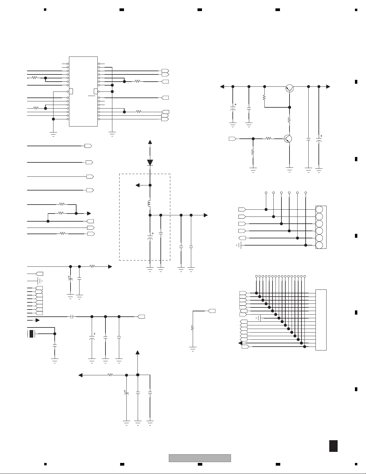
10.7 MAIN PCB ASSY (7/7)
A
B
2 3 4
C
D
E
F
36
X-HM20-K
1
2 3 4
Page 37
5
DA11
Must be populated all mode
C116
104P
2
C117
104P
10R
C120
104P
R94
2R2
R128
2R2
R133
2R2
C123
104P
C124
104P
R138
2R2
L1
100uH/1A
C152
0.1nF
C128
0.1nF
C161
0.1nF
C129
104P
R143
6K8
5K1
147
8K2
R30
6K8
C56 47uF
C136
47uF
R38
100K
R41
470R
C71
1uF
Q3
3904
R42
1K
C72
104P
Q13
SS8550
16
FCS-
15
TRK-
14
TRK+
13
FCS+
12
PD
11
VR
10
LD
9
GND
8
F
7
C
6
B
5
A
4
D
3
E
2
VCC
1
VREF
CN3
CON16_DA11
R134
0R
T32
T33
T34
T35
T36
T37
T38
T39
T40
T41
T42
T43
T44
T45
T46
T47
1
2
3
4
5
6
J13
CN06P/2.0
T27
T28
T29
T30
T31
T48
R120
15K
1
DO1.1
2
DO1.2
3
DI1.1
4
DI1.2
5
REG
6
REO
7
MUTE
8
GND1
9
DI2.1
10
DI2.2
11
DO2.1
12
DO2.2
13
GND
14
OPOUT
28
GND
27
DO4.2
26
DO4.1
25
DI4.2
24
DI4.1
23
VREF
22
VCC2
21
VCC1
20
DI3.2
19
DI3.1
18
DO3.2
17
DO3.1
16
OPIN+
15
OPIN-
2930
U7
SA1469PH
D1
1N4001
16.9344MHZ
C61
20P
C74
470uF
C127
47uF
C73
470uF
C126 220uF
R301
15K
MD
VCC1
3V3_CDA
B
A
C
D
F
E
VREF
3V3_CDA
3V3_CDA
VCC1
LD
VREF
SLEDGE
FOCUS
RADIAL
+6V5VCC
FOCUS
HOME_SW
V4
SPINDLE
SPINDLE
OTHER_3V3
CD_3V3
CD/DVD_ON
FOCRADRAD+
FOC+
MD
LD
VREF
VCC1
F
C
B
A
D
E
VR
SP+
SP-
SL+
SL-
HOME_SW
3V3_CDD
V4
SP-
SP+
FOC+
FOC-
MOTO_7V
7.5V/1.5A
VR
A
7/7
CD MECHA UNIT
(MOTOR)
CD MECHA UNIT
(PICKUP)
6 7 8
A
B
C
D
E
F
X-HM20-K
5
6 7 8
37
Page 38

1
iPod docking subboard connector
pitch1.25
Ipod docking subboard
IPOD_HW_CHARGE_CTL
IPOD_HW_CHARGE_CTL
C801
0.1uF
FB22
BLM18BB121SN1
FB23
NC
1
2
3
Q8 AP2301GN
R74
75.0K
R75
49.9K
R76
43.2K
R77
49.9K
1
2
3
Q10 AP2301GN
R78
10K
R81
10K
Q12
MMBT 3904
R84
4K7
R115
10K
1
2
J803
CON2_S
10
9
8
7
6
5
4
3
2
1
J802
CON10_S
R825
47K
IPOD_+
IPOD_+5V
IPOD_D+
IPOD_D-
DVD_USB_SEL
AGND
IPOD_D+
IPOD_D-
IPOD_+5V
IPOD_DET
ACC_POWER
DVD_USB_SEL
IPOD_VIDEO
IPOD_+5V
B
iPOD PCB ASSY
(92L36600201010)
B
C
CON704
A
4/7
J2
2 3 4
10.8 iPOD PCB ASSY (X-HM20 ONLY)
A
B
C
D
E
F
38
1
X-HM20-K
2 3 4
Page 39

Band rate:19200 or 57600(+/-2%)
iPOD 30pin Docking socket
1
DGND
2
DGND/MAIN_LINK_LANE0_RETURN
3
DP_ML_LANE0_P
4
USB_D+
5
DP_ML_LANE0_N
6
USB_D-
7
DP_ML_LANE1_P
8
USB_VBUS
9
DP_ML_LANE1_N
10
ACCE_IDENTIFY
11
DP_HOT_PLUG_DETECT/
12
F/W_PWR(FLOATING)
13
ACCESSORY_PWR(IPOD_OUTPUT)
14
RESERVED
15
DGND/AUXILIARY_CHANNEL_RETURN
16
DGND/MAIN_LANE1_LINK_RETURN
17
RESERVED
18
RX
19
TX
20
ACCE_DETECT
21
S_VIDEO_Y/COMPONENT_PR
22
S_VIDEO_C/COMPONENT_Y
23
COMPOSITE_VIDEO/PB
24
REMOTE_SENSE
25
LINE_IN_L/DP_AUX_CH_P
26
LINE_IN_R/DP_AUX_CH_N
27
LINE_OUT_L
28
LINE_OUT_R
29
AUDIO/VIDEO_RETURN
30
DGND
31
CHASSIS
32
CHASSIS
J801
IPOD_30PIN
R803
100R
C801
0.1uF
T15
T16
R801
100R
T3
C800
0.1uF
R802
47K
R45
0R
T6
R825
47K
IPOD_DET
IPOD_D+
IPOD_D-
IPOD_+5V
ACC_POW
IPOD_VIDEO
AGND
B
iPod
5
6 7 8
A
B
C
D
E
F
X-HM20-K
5
6 7 8
39
Page 40
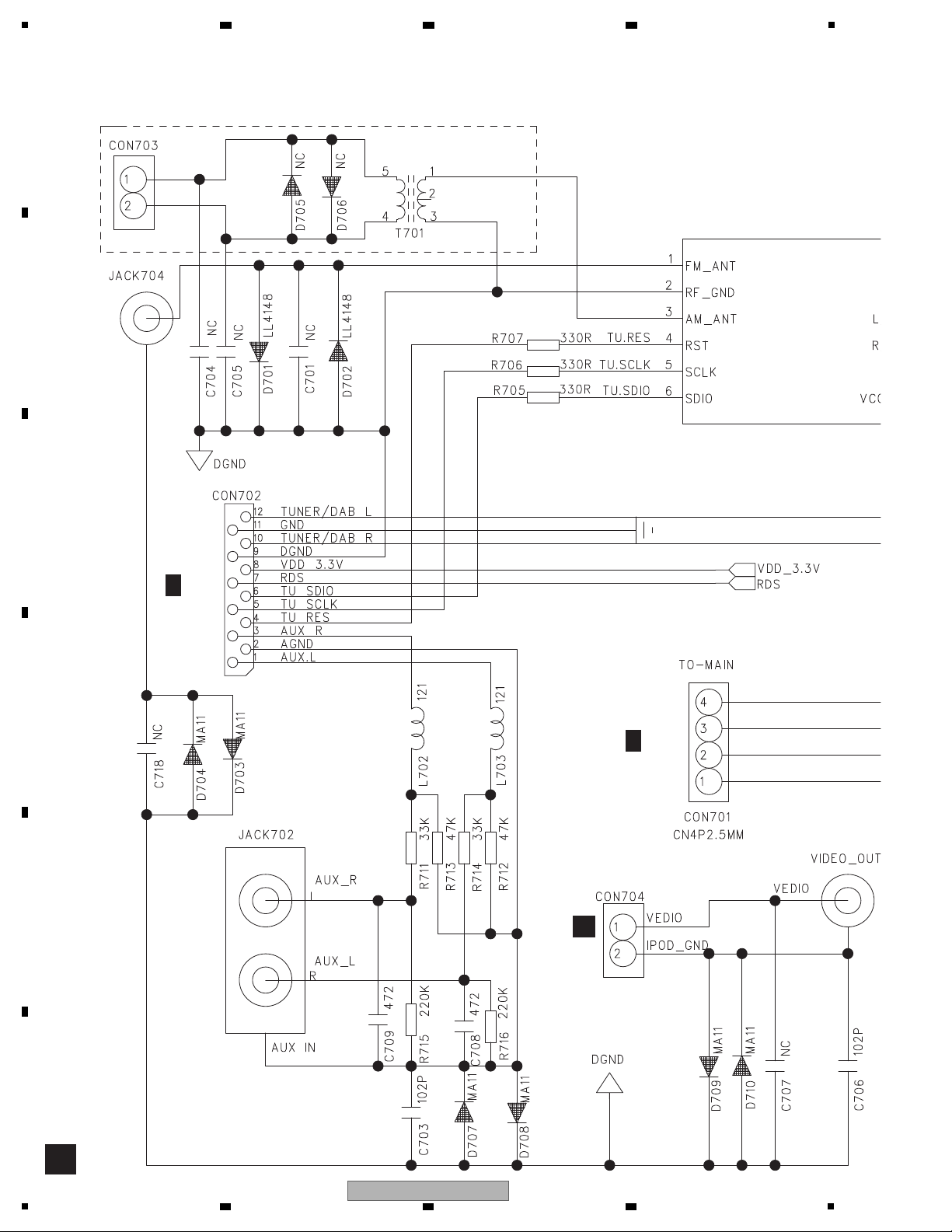
1
C
B
J803
A
5/7
J6
A
2/7
J1
Only for AM model
10.9 RADIO PCB ASSY
A
B
2 3 4
C
D
E
F
40
1
2 3 4
X-HM20-K
Page 41
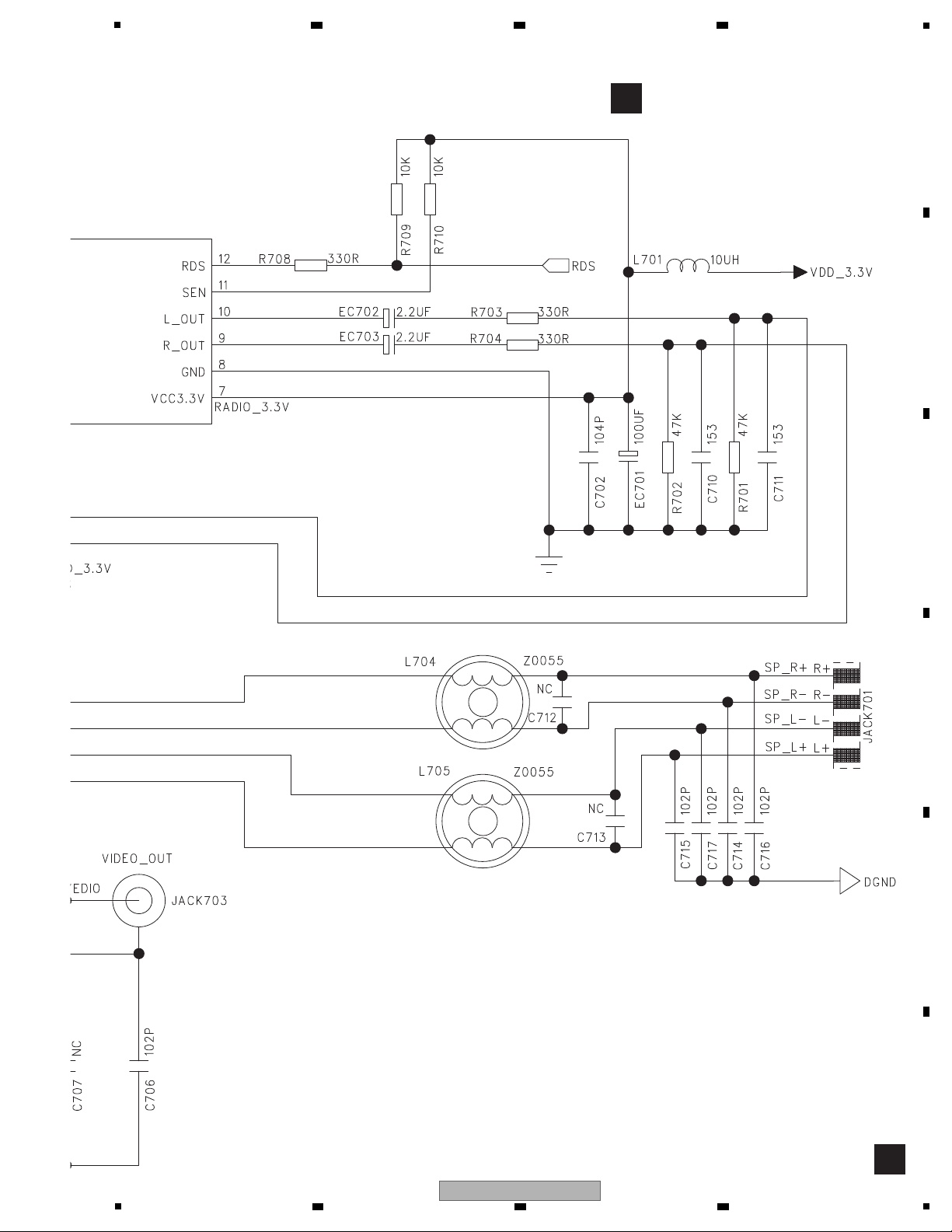
5
C
RADIO PCB ASSY
(X-HM20: 92L36400201010)
(X-HM10: 92L36400101010)
C
6 7 8
A
B
C
D
E
F
X-HM20-K
5
6 7 8
41
Page 42

1
D
DISPLAY PCB ASSY
(X-HM20: 92L36500201010)
(X-HM10: 92L36500101010)
D
A
6/7
J14
10.10 DISPLAY PCB ASSY
A
B
2 3 4
C
D
E
F
42
1
2 3 4
X-HM20-K
Page 43

5
D
6 7 8
A
B
C
D
E
F
X-HM20-K
5
6 7 8
43
Page 44
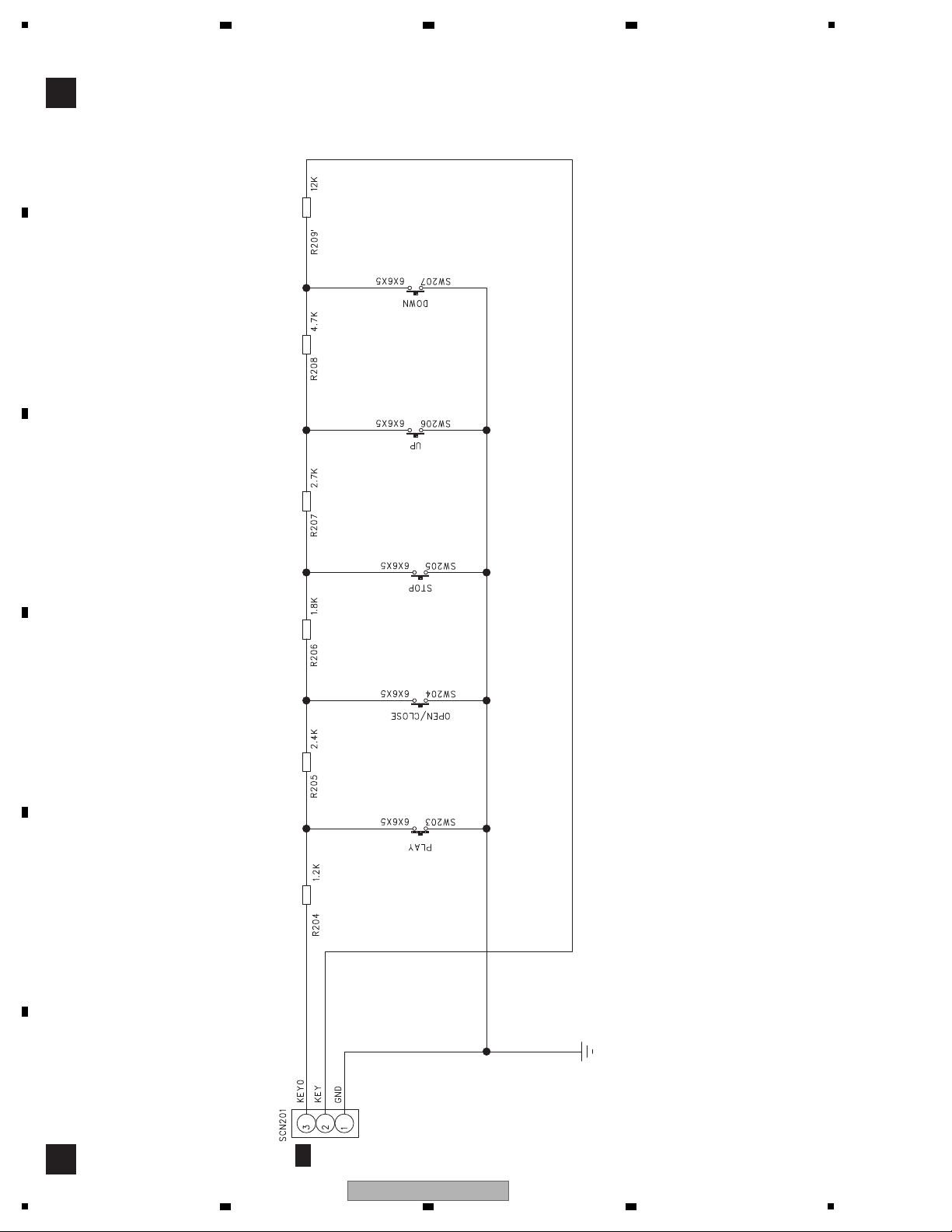
1
E
KEY-SWITCH PCB ASSY
(X-HM20: 92L37200201010)
(X-HM10: 92L37200101011)
E
A
6/7
J5
10.11 KEY-SWITCH PCB ASSY
A
B
2 3 4
C
D
E
F
44
1
2 3 4
X-HM20-K
Page 45

5
6 7 8
10.12 HEADPHONE PCB ASSY
HEADPHONE PCB ASSY
F
(X-HM20: 92L37100201011)
(X-HM10: 92L37100101011)
J3
6/7
A
A
B
C
D
E
F
F
X-HM20-K
5
6 7 8
45
Page 46

1
A
3/7
J11
A
3/7
J9
G
Only for DVD model
10.13 POWER PCB ASSY
A
B
2 3 4
C
D
E
F
46
X-HM20-K
1
2 3 4
Page 47

5
G
POWER PCB ASSY
(X-HM20: 92L36800201010)
(X-HM10: 92L36800101010)
G
6 7 8
A
B
C
D
E
F
X-HM20-K
5
6 7 8
47
Page 48

1
H
USB PCB ASSY
(X-HM20: 92L36900201011)
(X-HM10: 92L36900101011)
H
A
4/7
J12
10.14 USB PCB ASSY
A
B
2 3 4
C
D
E
F
48
1
2 3 4
X-HM20-K
Page 49

5
6 7 8
A
B
C
D
E
F
X-HM20-K
5
6 7 8
49
Page 50
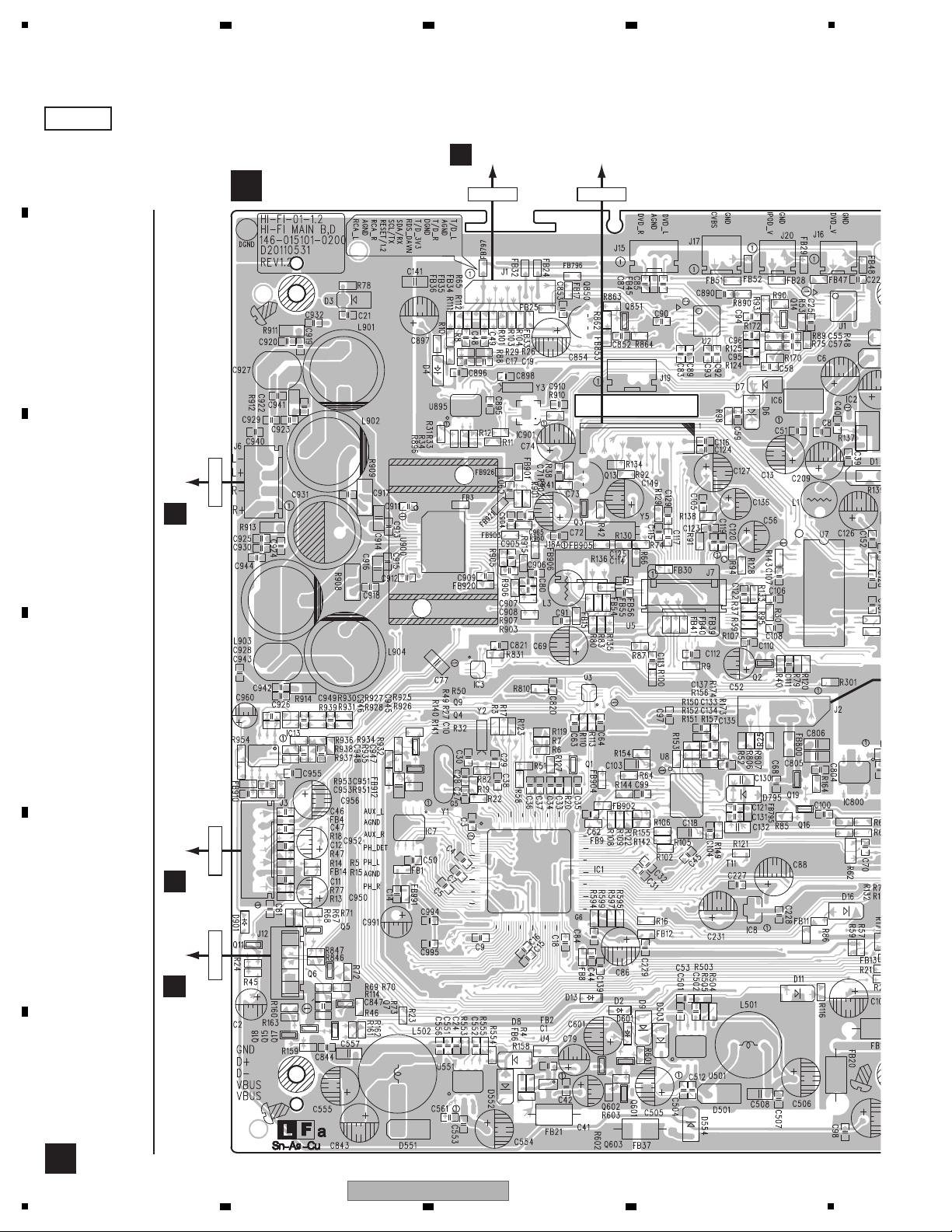
1
A
A
MAIN PCB ASSY
SIDE A
C
CON701
J6
H
SCN801
J12
F
SCN802
J3
C
CON702
J1
CD MECHA
UNIT (PICKUP)
CN3
IC901
Q851 Q14
IC6
U7
U2
U1
U895
Q850
Q13
Q3
Q2
IC3
U3
Q16
IC800
Q19
Q1
U8
U5
IC1
IC7
Q9
Q4
IC8
U501
Q601
U551
U4
Q7
Q18
Q17
Q15
Q5
Q11
Q12
IC13
U900
2 3 4
11. PCB CONNECTION DIAGRAM
11.1 MAIN and iPOD PCB ASSYS
A
B
C
D
E
F
50
X-HM20-K
1
2 3 4
Page 51

5
BA
B
iPOD PCB ASSY
SIDE A
G
CON402
J9
E
SCN201
J5
D
CON201
J14
CD MECHA
UNIT (MOTOR)
J13
LOADER
ASSY
J10 J2
J802
G
CON401
J11
C
CON704
J803
NOTE FOR PCB DIAGRAMS :
1. The parts mounted on this PCB include all
necessary parts for several destinations.
For further information for respective destinations, be sure to check with the schematic diagram.
CapacitorConnector
P.C.Board Chip Part
SIDE A
SIDE B
2. View point of PCB diagrams.
Q8 Q10 Q12
6 7 8
A
B
C
D
E
F
X-HM20-K
5
6 7 8
51
Page 52
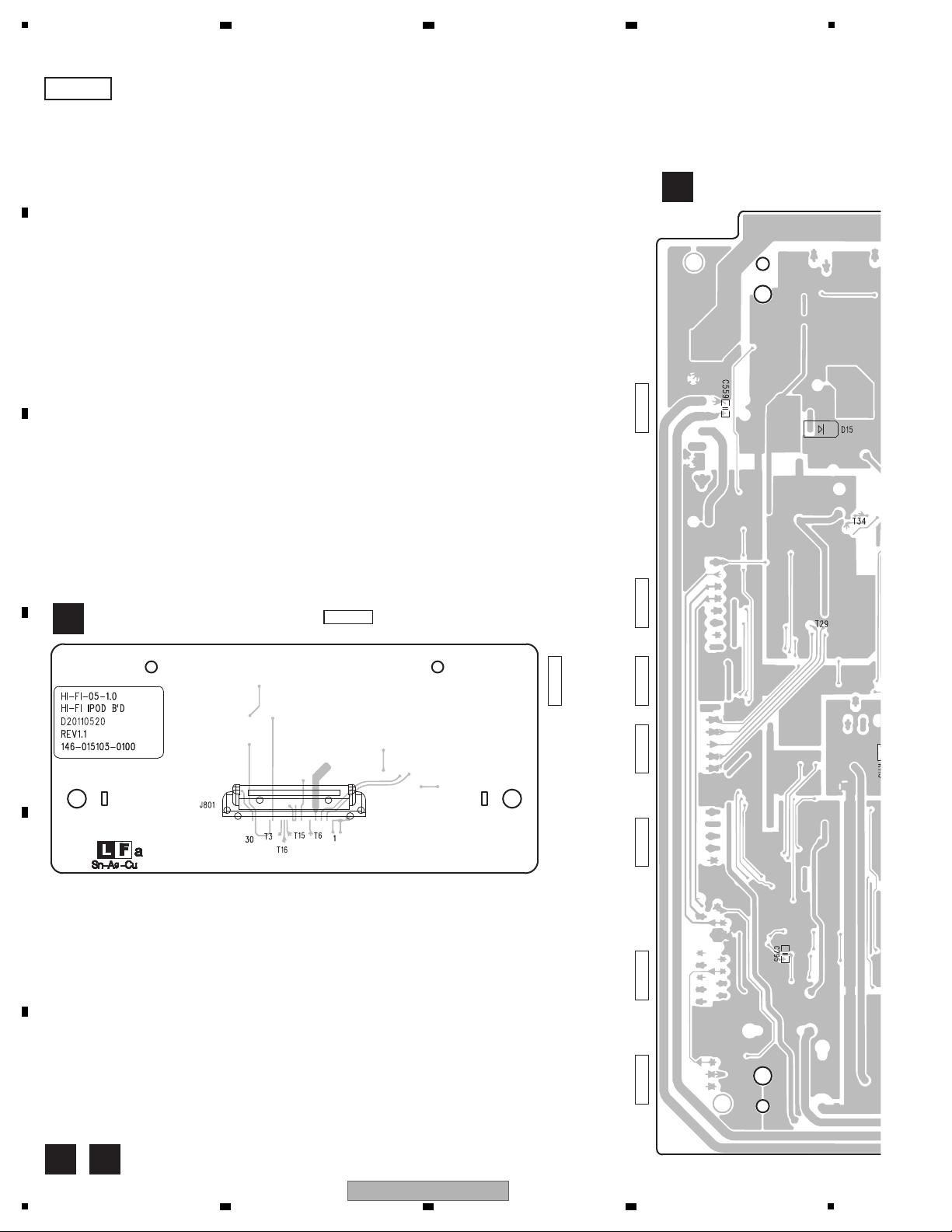
A
BA
A
MAIN PCB ASSY
B
iPOD PCB ASSY
SIDE B
J9J5 J14 J13J10 J2
J802
J11
J803
B
1
2 3 4
C
D
E
F
52
1
2 3 4
X-HM20-K
Page 53

5
A
SIDE B
J6J12 J3
J1CN3
IC795
IC902
IC4
Q8
Q10
Q420
6 7 8
A
B
C
D
E
F
X-HM20-K
5
6 7 8
53
Page 54
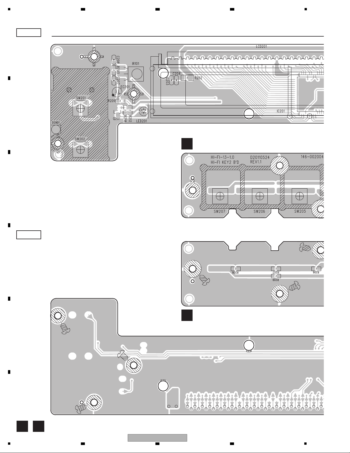
1
E
KEY-SWITCH PCB ASSY
E
KEY-SWITCH PCB ASSY
ED
SIDE A
SIDE B
Q201 IR101 IC201
2 3 4
11.2 DISPLAY and KEY-SWITCH PCB ASSYS
A
B
C
D
E
F
54
X-HM20-K
1
2 3 4
Page 55
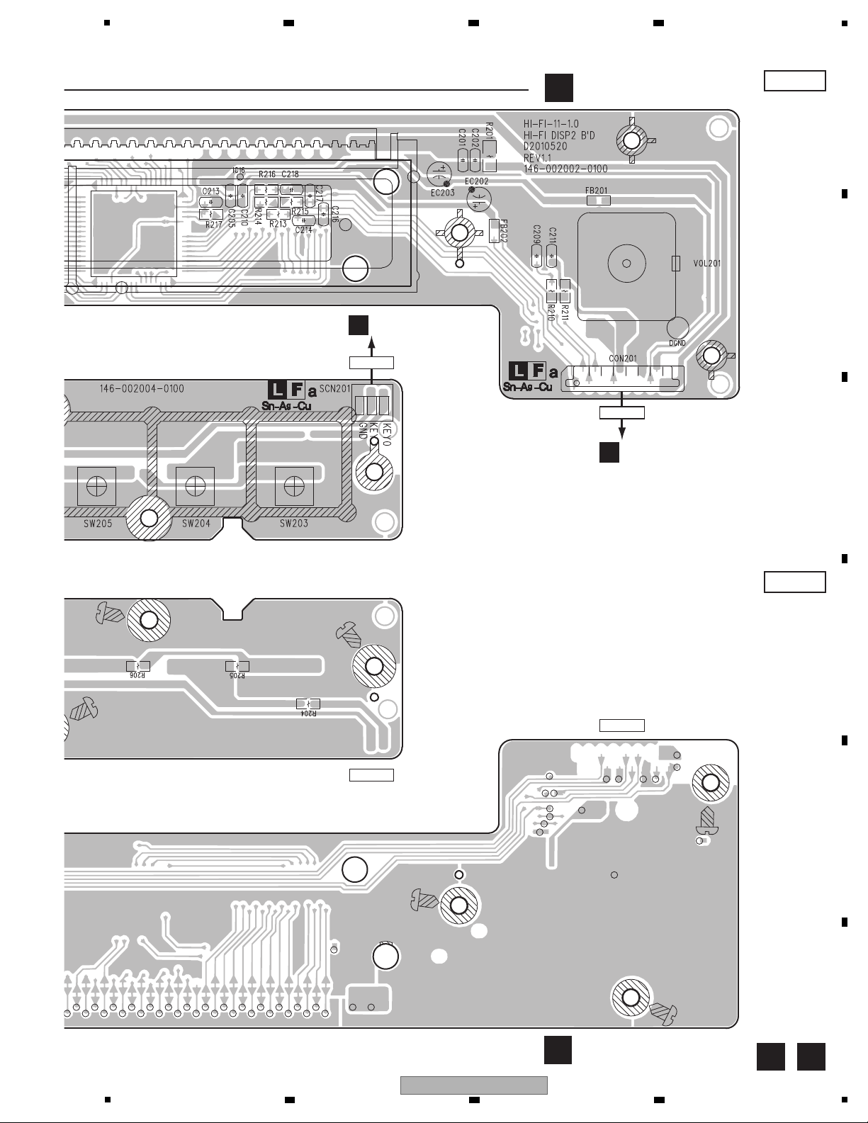
5
D
DISPLAY PCB ASSY
D
DISPLAY PCB ASSY
A
J14
CON201
A
J5
SCN201
ED
SIDE A
SIDE B
IC16
CON201
SCN201
6 7 8
A
B
C
D
E
F
X-HM20-K
5
6 7 8
55
Page 56

1
C
SIDE A SIDE A
SIDE B SIDE B
C
RADIO PCB ASSY
C
RADIO PCB ASSY
A
J1
CON702
B
J803
CON704
CON704
A
J6
CON701
CON702 CON701
IC701
2 3 4
11.3 RADIO PCB ASSY
A
B
C
D
E
F
56
X-HM20-K
1
2 3 4
Page 57

5
6 7 8
11.4 HEADPHONE and USB PCB ASSYS
SIDE A SIDE A
A
HEADPHONE PCB ASSY
F
J3
A
SCN802
USB PCB ASSY
H
J12
A
SCN801
B
C
SIDE B SIDE B
HEADPHONE PCB ASSY
F
SCN802 SCN801
USB PCB ASSY
H
D
E
F
HF
X-HM20-K
5
6 7 8
57
Page 58

1
G
SIDE A SIDE A
G
POWER PCB ASSY
A
J11
A
J9
CON401
CON402
AC IN
JACK401
IC401
Q401
Q402
IC402
11.5 POWER PCB ASSY
A
2 3 4
B
C
D
E
58
X-HM20-K
1
2 3 4
F
Page 59

5
6 7 8
SIDE B SIDE B
POWER PCB ASSY
G
JACK401
A
B
C
D
E
CON401
CON402
F
G
X-HM20-K
5
6 7 8
59
 Loading...