

Page 1
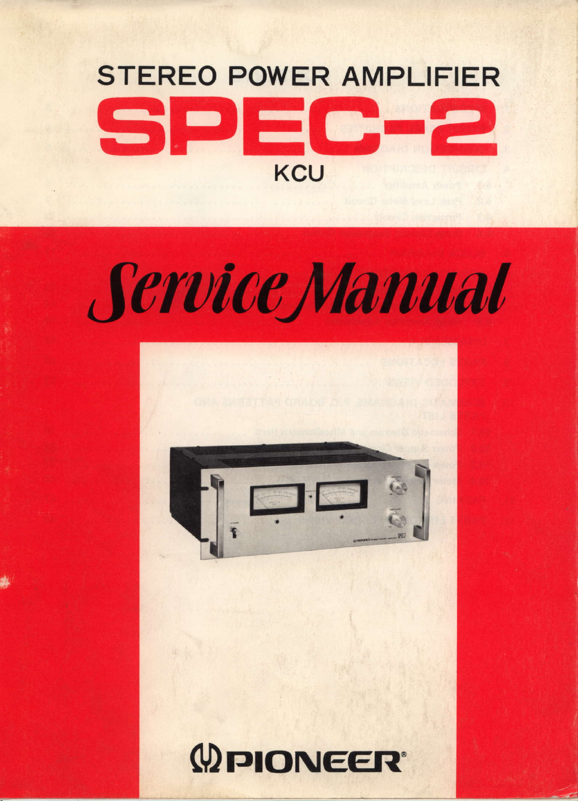
STEREO POWER
AMPLIFIER
SPEGI?,
KCU
(DrrroNEER'
Page 2
CONTENTS
1.
SPEC|F|CAT|ONS
2.
FRONT
3.
CoNNECTION
4.
CIRCUIT
4.1
4.2
4.3
4.4 Surge Current
BLOCK
5.
ADJUSTING
6.
6.1
6.2 Current
6.3
D|SASSEMBLY
7.
PARTS LOCATTONS
8.
9.
EXPLODED
PANEL FACILITIES
DESCRIPTION
Power
Peak Level Meter Circuit
Protection Circuit ,
ldle Current Adiustment
Meter Amplifier
Amplifier
DIAGRAM ...
PROCEDURES
VIEWS
.....
DIAGRAM
Suppressor
Limiter
Sensitivity
Adjustment
Circuit .
Adiustment
... ... ..
.. .......
'........
......
....'...
. .
......
.. . 16
...
........
3
4
5
6
7
8
10
11
13
. . 14
15
20
23
10.
SCHEMATIC
PARTS LIST
10.1 Schematic
Power
10.2
10.3 Power Amplifier Assembly
Meter Amplifier Assembly
10.4
PACKING
11.
PARTSLISTOFEXPLODEDVIEWS.
12.
DIAGRAMS,
Diagram
Supply
Circuit Assembly
P.C. BOARD
and Miscellaneous
PATTERNS AND
Parts ..
(AWR-093)
(AWH-045)
(AWM-0811
.......
'... 33
....
-. '. 37
..
' ' 42
. .
......
.........48
... 47
30
Page 3
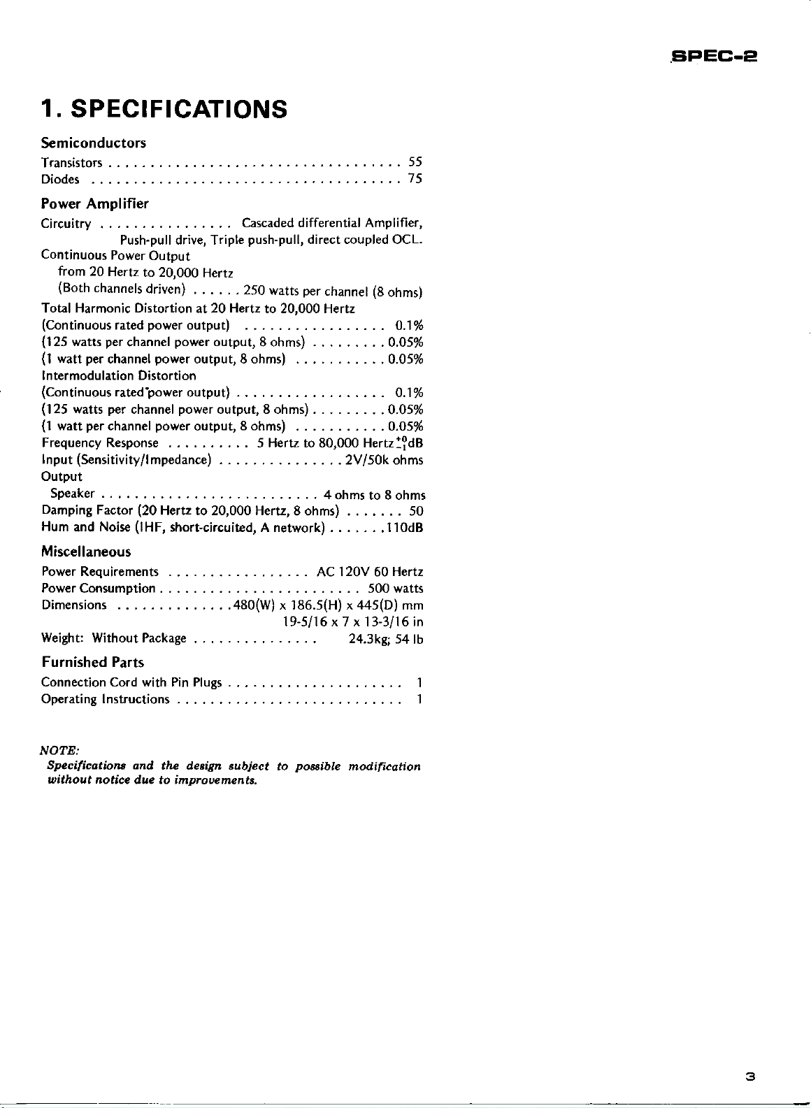
1.
SPECIFICAT|ONS
Semiconductors
Transistors
Diodes ..
...........55
...........75
Power Amplifier
Circuitry
Continuous
from
(Both
Total Harmonic Distortion
(Continuous
(125
(1
watt
.
20
Hertz
channels
per
watts
per
channel
Push-pull drive, Triple
Power
rated
channel
.......
Outout
to 20,000
driven)
power
. .
at20
output)
power
poweroutput,8
lntermodulation Distortion
(Continuous
(125
(1
watt
Frequency Response
Input
rated'power
per
watts
per
channel
channel
output) ......... - O."lo/o
power
power
output,
. 5 Hertz to 80,000 HertzlldB
(Sensitivity/lmpedance)
Output
Speaker..
Damping
Hum
and
(20
Factor
(lHF,
Noise
Hertz to 20,000 Hertz,
short-circuited,
Miscellaneous
Power Requirements .
Power
Consumotion . . . . . . .,.. 500watts
Dimensions
Weight:
Without Package
......480(W) x186.5(H) x445(D) mm
.
Cascaded differential Amplifier,
push-pull,
Hertz
. . . . 250
Hertz
output,8
to 20.000 Hertz
direct coupled OCL.
per
watts
channel
ohms) . ........O.O5%
ohms) . . . . . . .
output, S ohms) ..
8 ohms)
.
..
. . . .O.O5%
. . . . . . 2Vl50k ohms
.
4ohmstoSohms
S ohms) ...,... 50
A network) . . . . . .
. AC 120V 60
19-5/16 x 7 x13-3116in
-....0.05%
Furnished Parts
Connection Cord with Pin Plugs
Operating lnstuctions
(g
ohms)
o.1%
, . . . 0.Q5o/o
.110d8
Hertz
24.3kg;
54lb
EiPEC.E
NOTE:
Specificdtiotrt and
without notice
the design subject
due to improuements.
possible
to
mod,fication
Page 4
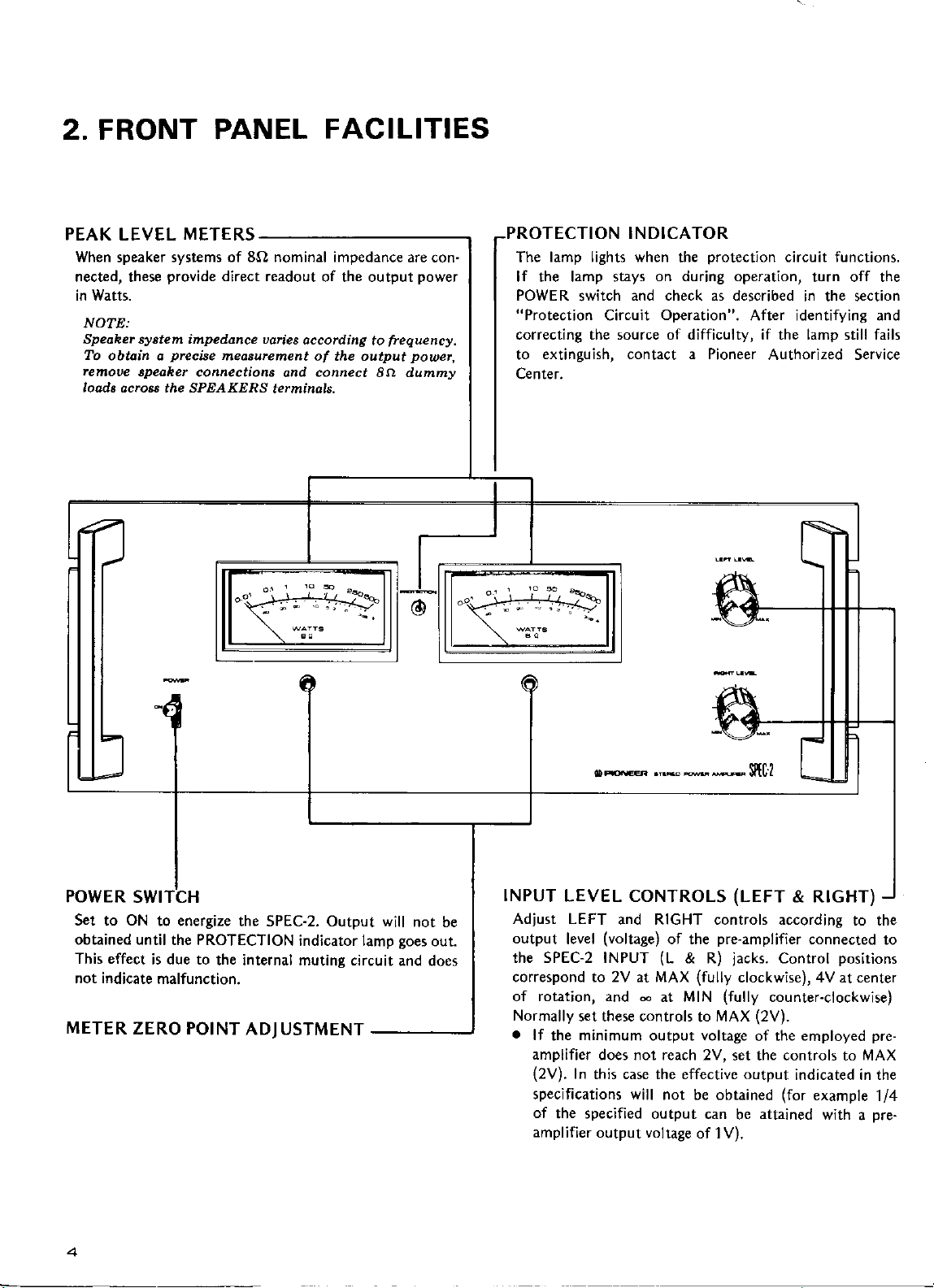
2. FRONT PANEL
FACILITIES
PEAK LEVEL
When
speaker
nected, these
in Watts.
NOTE:
Speoher syotem impedance uaries
To
obtoin o
remoue
loods ocro4i the SPEAKERS
METERS
systems of 8O nominal impedance
provide
preciae
Spedher con\ectiotrs
direct readout
medsurcment
of the output
occording
of the output
connect
ond
termindls-
are con-
power
to
frequency.
poue\
8a dumtuy
PROTECTION INDICATOR
lamp lights when
The
lf the lamp stays
POWER
"Protection
correcting the source of difficulty, if the lamp still fails
to
Center,
switch
Circuit
extinguish, contact a Pioneer
on during operation,
and check as described
protection
the
Operation".
circuit functions.
turn off the
in the section
After identifying and
Authorized Service
POWER
S'et to ON
obtained until
This effect
not indicate
METER
SWI CH
ZERO POINT
to energize
the PRoTEcTIoN
is due to
malfunction.
the SPEC-2. Output will
the internal muting
ADJ USTMENT
indicator lamp
circuit and does
not be
Soes
out.
INPUT
Adjust LEFT
output
the SPEC-2 INPUT
correspond to 2V
of rotation, and d
Normally
.
LEVEL CONTROLS
and RIGHT controls according
(voltage)
level
MAX
at
set these controls
lf
the minimum output voltage
amplifier
(2V).
specifications will
of
amplifier
does not reach 2V.
In
this case the effective output
the specified
output voltage
output can
(LEFT
of the
(L
at MIN
not be obtained
pre-amplifier
jacks.
& R)
(fully
clockwise), 4V at center
(fully
(2V).
MAX
to
of the
set the controls to MAX
attained
be
of 1V).
& RIGHT)
to the
connected to
Control
counter-ciockwise)
(for
positions
a
pre-
1/4
pre-
employed
indicated in the
example
with
Page 5
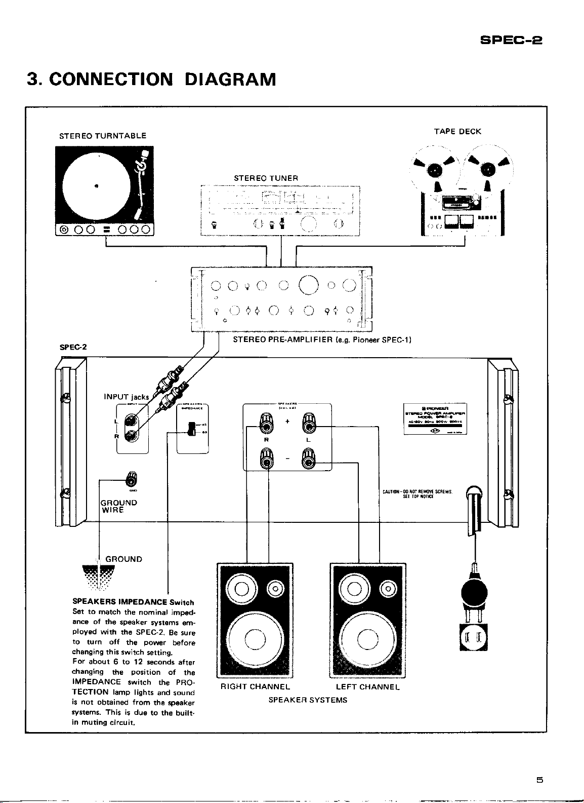
sPEC-e
3.
CONNECTION
STEREO
TURNTABLE
DIAGRAM
-i
;
. , 1 I , r ,
rl
tO
C
STEREO
PRE-AMPLIFIER
'\..,,
i
O
q1
(e.s.
o
Pioneer
TAPE DECK
SPEC-1)
SPEAKERS
S€t to
ance
ployed
to
turn otf
chenging
For
changing
IMPEDANCE
TECTION lamp
is
not obtained from
systems. This is du6
in muting
IMPEDANCE
malch
of the
spoaker
with
the SPEC-2.
this switch
about
6 to 12 seconds
the
circuit,
the nominal imDed-
the
position
swirch the PRO-
lights
syst€ms
po!!€r
setting.
o{
and sound
the speaksr
to
the built-
swilch
em-
Be sure
before
6tter
the
RIGHT
CHANNEL
SPEAKER
LEFT CHANNEL
SYSTEMS
Page 6
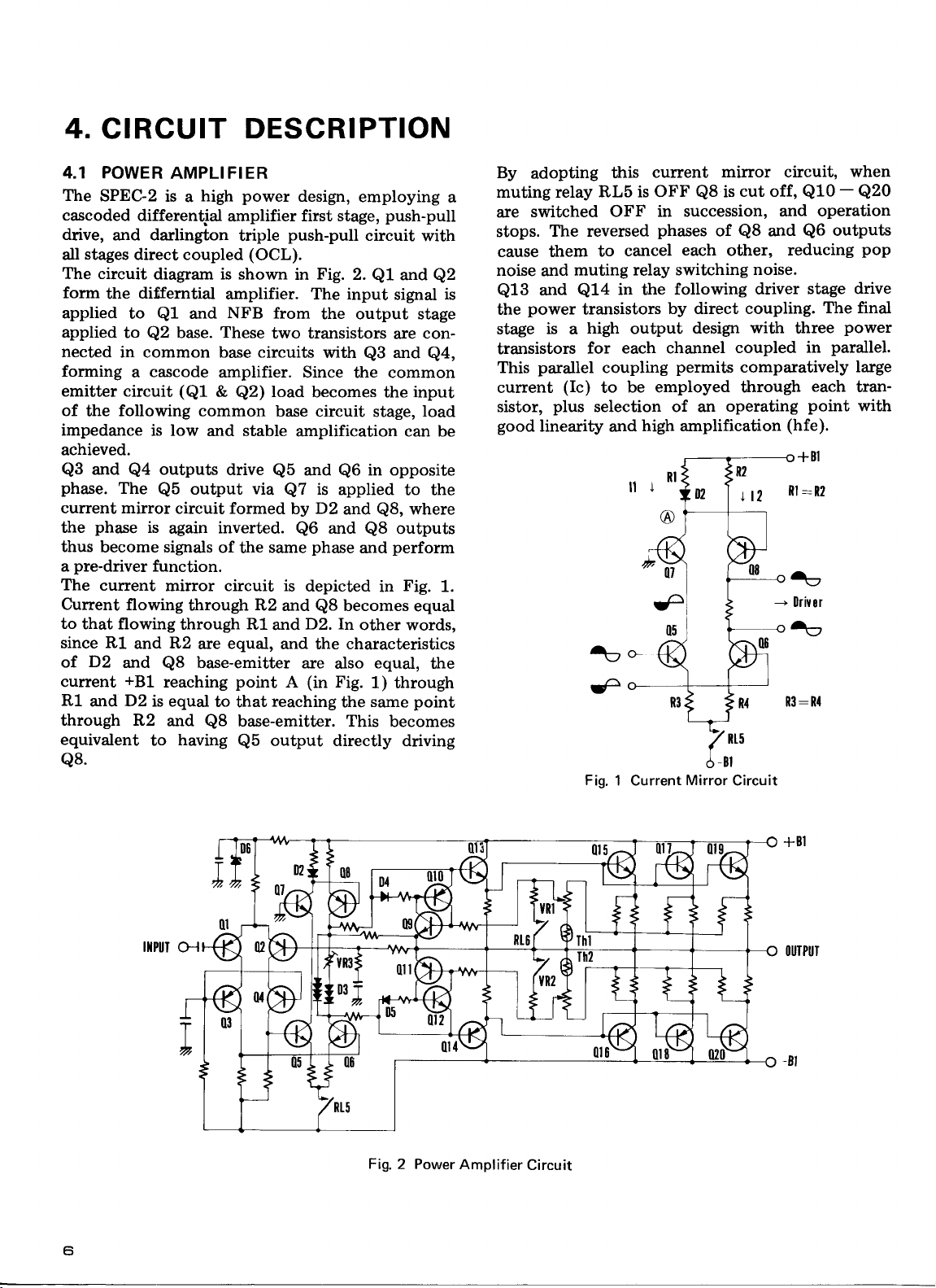
4.
CIRCUIT
DESCRIPTION
4.1 POWER
The
SPEC-2
cascoded
drive,
all
The circuit
form
applied
applied
nected
forming
emitter circuit
of
impedance
achieved.
Q3
phase.
current mirror
the
thus
a
The
Current
to
since
of.
current
R1
through R2
equivalent
Q8.
and darlington
stages
the
in common base circuits
the following common
and
The
phase
become signals
pre-driver
cunent
that flowing
R1
D2
and
AMPLIFIER
high
is
a
differential
direct coupled
diagram is shown
differntial
to
to
a
Q4
flowing
and
and
+BL
D2
and
Q1
base.
Q2
cascode
(Q1
is low
Qb
is
function.
is equal
to
and stable
outputs
output
circuit formed
again
mirror circuit is
through R2
through Rl
R2
are
base-emitter
Q8
reaching
and
Q8
having
power
amplifier
triple
(OCL).
amplifier. The input
NFB
These
amplifier. Since
&
Q2)
drive
inverted.
of
the
equal,
point A (in
to
that
base-emitter. This
Q5
design,
first stage,
push-pull
Fig.
in
from
two transistors
load
base circuit
amplification can be
Q5
via
Q7
by
Q6
same
and
and
and the characteristics
are
reaching
output directly
2.
the output stage
with
the common
becomes the input
and
Q6
is
applied
D2
and
and
phase
depicted
becomes
Q8
In
D2.
also
Fig.
the
employing
push-pull
circuit
Q1
Q3
stage,
in opposite
Q8
and
other words,
1) through
same
and
signal
are con-
and
to the
where
Q8,
outputs
perform
Fig.
in
equal
equal,
point
becomes
driving
with
Q2
Q4,
load
1.
the
By
adopting
muting relay
a
is
switched
are
stops.
cause them
noise
Q13
the
stage
transistors
This
current
sistor,
good
The reversed
and
and
power
is
parallel
linearity
RLb is OFF
to
muting
Q14
transistors
high
a
for
coupling
(Ic)
to
plus
selection of an
current
this
OFF in succession,
phases
cancel
relay switching
in the following
by direct coupling.
output
each channel
be employed through
high amplification
and
mirror circuit,
is
Q8
of
each
other,
design
coupled
permits
operating
cut off,
and operation
and
Q8
reducing
noise.
driver
with
three
comparatively
(hfe).
+Bl
ll:t2
-
llrirel
when
Q10 - Q20
outputs
Q6
stage drive
in
each
point
pop
The final
power
parallel.
large
tran-
with
tu
€
Fig.
1 Current
Mirror
Circuit
IIIPUTH
Fig.
Power
2
Amplifier
Circuit
Page 7
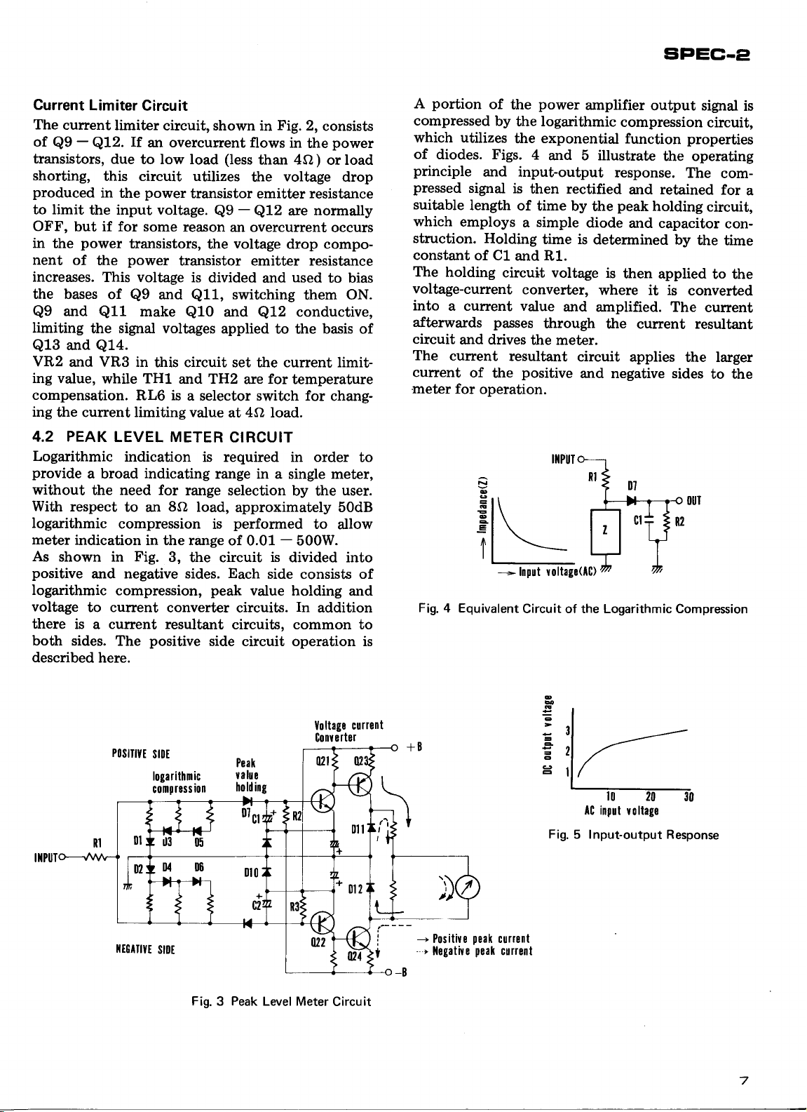
Current
The
of
transistors,
shorting,
produced
to limit
OFF,
in
nent
increases.
the
Q9
limiting
Q13
VR2
ing value,
compensation.
ing
current
-
Q9
Limiter
qLz.
Circuit
limiter
If
an overcurrent
due
to low load
circuit, shown in
this circuit utilizes
in the
power
the input voltage.
but if for
power
the
of
the
some rea.son
transistors,
power
This voltage
bases of
and
Ql1
the
and
Q14.
and VR3 in
and
Q9
make
signal voltages
this circuit set the current limit-
while TH1
RLG is
the current limiting value
Fig.
2,
consists
power
the
4S2)
or load
resistance
occurs
drop
(less
transistor
-
Q9
an overcurrent
voltage
the
flows in
than
voltage
the
emitter
are normally
Q12
drop compo-
transistor emitter resistance
is
divided
switching
Q11,
and
Q10
applied
and TH2
are
a selector switch for
4O
at
used
and
them
conductive,
Q12
to the basis of
for
temperature
load.
to bias
ON.
chang-
portion
A
compressed
of
by
which utilizes
of
diodes. Figs.
principle
pressed
suitable
which
struction.
constant
and input-output
signal
length
employs
Holding
of C1
The holding
voltage-current
into
a current value
afterwards
circuit
The
current
current
.meter
passes
and drives
of
the
for
operation.
pov/er
the
amplifier
the logarithmic
exponential
the
4
and 5 illustrate
is
then rectified
of
time by
simple
a
the
diode
time is
and R1.
circuit voltage
converter,
and
through
the meter.
resultant
positive
circuit applies
and negative sides
SPEC-p
output signal
compression
function
the operating
response.
and retained
peak
holding
and capacitor
determined
is
then applied
where it is
amplified. The
the current resultant
circuit,
properties
The
circuit,
by
ttre time
to the
converted
current
the larger
to the
comfor
con-
is
a
4.2 PEAK
Logarithmic
provide
without
With
a broad indicating
the
respect
logarithmic
meter
indication
As
shown in Fig.
positive
and negative sides. Each
logarithmic
voltage
there
both
described
to current
is a cunent resultant
sides. The
here.
LEVEL METER
indication
is required in order
range in a
need for
to
compression
an
8O
range
load,
is
in the range
3,
the circuit
compression,
peak
converter circuits.
positive
PostTtvt
stDE
logarithmic
comp
side circuit operation is
ion
ress
CIRCUIT
single meter,
selection by the
user.
approximately 50dB
performed
to
allow
of 0.01 - 500W.
is
divided into
side
consists
value
holding and
In
addition
circuits, common to
current
Yoltage
rter
Conv e
Peak
r alue
ho ld ing
to
of
Fig.
4 Equivalent
o
E
I\ f
o
e
I
EL
+
Inprt voltagc(lC)
Circuit of the Logarithmic Compression
e
4
=
e
e
€
o
E
Fig.
lC input
voltage
5 Input-output Response
It0lltvt
st0t
Fig. 3 Peak
Level Meter
Circuit
-
Positive
--'
llegatiYe
peak
current
peal
current
7
Page 8
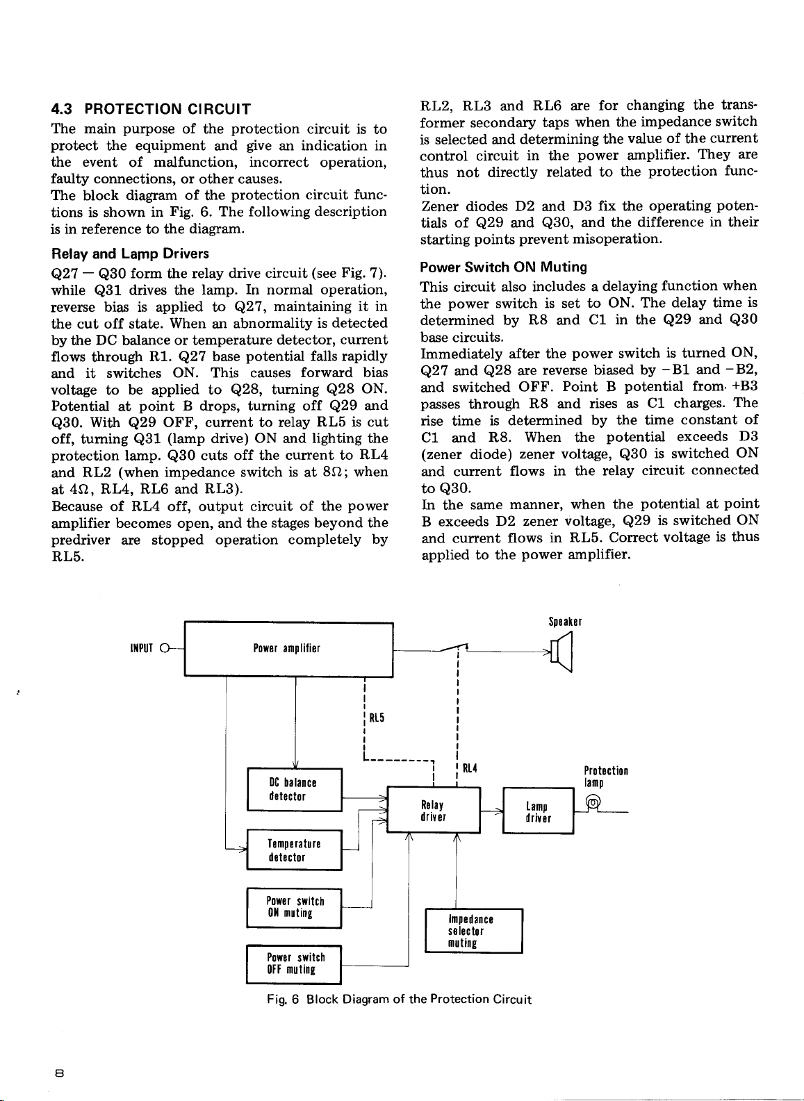
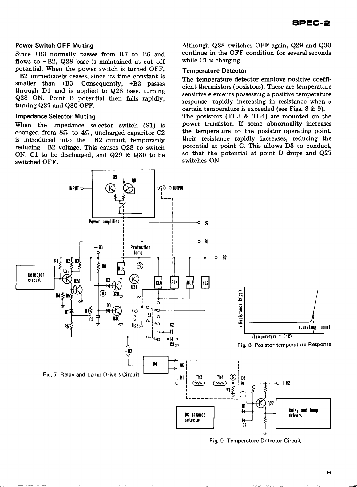
PROTECTION
4.3
The main
protect
the event
purpose
equipment
the
of
malfunction, incorrect
faulty connections,
The block
tions
in
is
reference to
Relay and
-
q27
while
reverse
the cut
by the
flows through
and
voltage
Potential
Q30.
off, tuming
protection
RL2
and
4Q, RL4, RL6 and
at
Because of
amplifier
predriver
diagram of
Fig.
is shown
in
the
Lamp Drivers
form
Q30
Q31
the
drives
bias is applied to
off state.
DC
balance
When
R1.
it switches
be
to
at
With
Q29
lamp.
(when
ON. This causes
applied
point
OFF, current to
(lamp
Q31
Q30
impedance switch
RL4
off, output
becomes open, and the
are stopped operation
RL5.
CIRCUIT
of the
protection
give
and
or other causes.
protection
the
The following description
6.
dia$am.
relay drive
lamp.
the
circuit
In
Q27,
abnormality
an
or
temperature
potential
base
Q27
to
Q28,
B
drops, turning
drive)
ON
cuts off the
RL3).
circuit of the
circuit is
to
an indication in
operation,
circuit func-
(see
Fig.
7).
normal operation,
detected
is
current
it in
maintaining
detector,
falls rapidly
forward bias
turning
off
RL5 is
relay
lighting
and
current to
is
at
Q28
Q29
8Q;
ON.
and
cut
the
RL4
when
power
stages beyond the
completely
by
RLg
RL2,
former
selected and
is
control
not directly
thus
and
secondary
circuit
tion.
Zener
tials
starting
Power
This circuit
the
diodes
of
Q29
points
Switch
power
and
also includes a
switch is set to
determined by
base circuits.
Immediately
and
Q27
switched
and
passes
rise
time
C1 and
(zener
and current
to
Q30.
In
the
B exceeds
current
and
applied
after the
Q28
through
is determined
R8.
diode)
flows in the
manner,
same
D2 zener
flows
to the
RL6
are
when the
taps
determining
in the
power
related to
D2
prevent
ON
R8
DB
and
and the
Q30,
misoperation.
Muting
and
C1 in the
power
reverse biased by
are
OFF.
Point
R8 and
rises as
by the
When
zener
the
voltage,
when the
voltage,
in RL5.
power
amplifier.
changing
for
impedance
value of
the
amplifier.
the
fix
the
difference
delaying
ON. The
switch
potential
B
potential
Q30
circuit
relay
potential
Q29
Correct
the
switch
current
the
They
protectiorr
operating
poten-
in
function
delay time
and
Q29
is
turned
-B1
and
from'+B3
Cl charges.
constant
time
exceeds
is switched
connected
at
is switched
voltage
is thus
trans-
are
func-
their
when
is
Q30
ON,
-B2,
The
of
D3
ON
point
ON
Fig.
6 Block
Diagram of the
Protection
Circuit
Page 9
SPEG.El
Power
Since
flows to
potential.
-B2
smaller
through Dl
Q28
tuming
lmpedance
When
changed
is
reducing
ON,
switched
Switch
+B3
OFF
normally
-B.2,
Q28
When the
immediately
than
+83.
and is
ON. Point B potential
and
Q27
Q30
Selector Muting
the impedance
from 8Sl
introduced into
-B2
voltage.
C1
to be discharged,
OFF.
Muting
passes
from
base is maintained
power
switch is
ceases, since its
Consequently,
applied
to
Q28
then falls rapidly,
OFF.
selector
4Sl, uncharged
to
-
82
the
This
circuit,
causes
and
Q29
R7
to
at cut
tumed OFF,
time
constant
+83
base, tuming
switch
capacitor
temporarily
to switch
Q28
&
Q30
R6
passes
(S1)
to
and
off
is
is
C2
be
Although
continue
switches OFF
Q28
in
the
OFF
condition
again,
Q29
for several seconds
while C1 is charging.
Temperature
The temperature detector
cient thermistors
sensitive elements
Detector
employs
(posistors).
possessing a positive
positive
These are temperature
temperature
response, rapidly increasing in resistance
(see
certain
The
power
the
their
potential
so that the
temperature
posistors (TH3
transistor.
temperature to the
resistance rapidly increases,
point
at
potential
is exceeded
TH4)
&
If
some abnormality
are mounted
posistor
C. This allows
point
at
Figs.
operating
reducing the
DB
to conduct,
D drops and
switches ON.
and
Q30
coeffi-
when a
8 &
9).
on the
increa.ses
point,
Q27
q
4
o
,2
o
4
A
-Tem0erature
Posistor-temperature
Fig. 8
Fig.
9 Temperature Detector Circuit
point
("
t
Response
Page 10
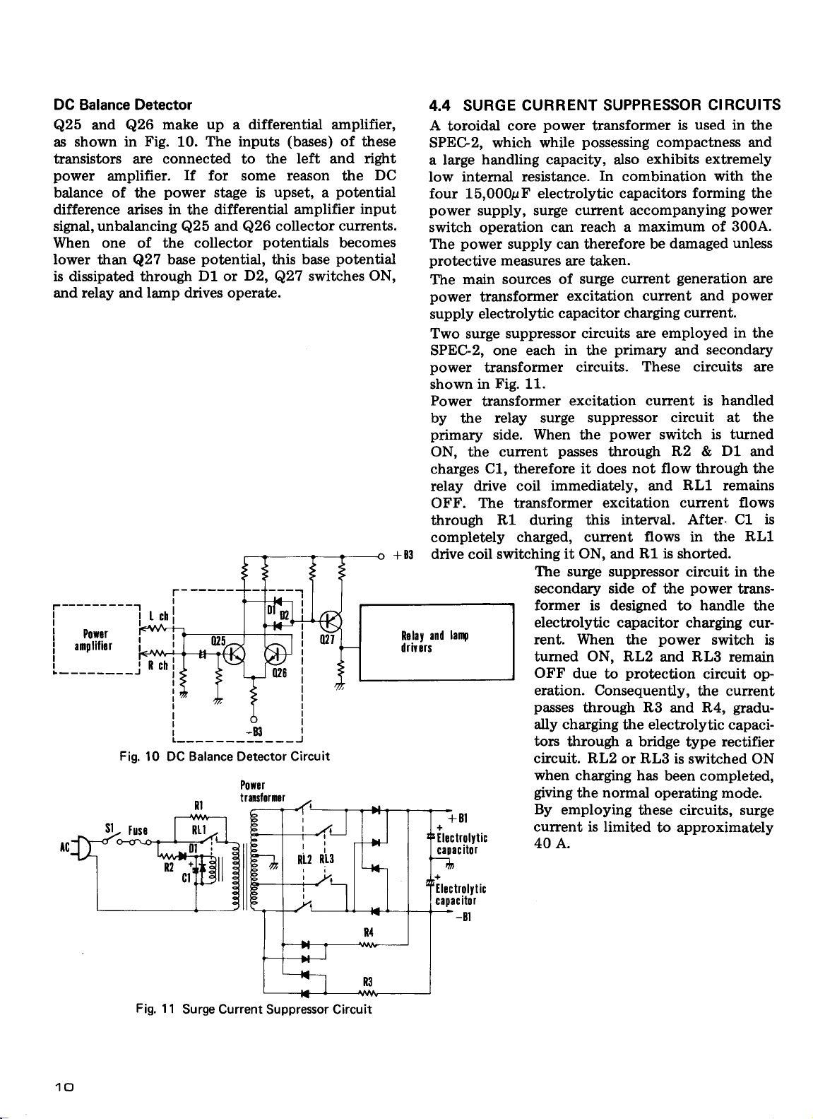
DC
Balance
and
Q25
as shown
Detector
make up a differential amplifier,
Q26
Fig.
in
The inputs
10.
transistors are connected to the
power
balance of
amplifier.
the
difference arises in
signal, unbalancing
When one
lower
than
of
Q27
is dissipated through
and relay
and
If
for
power
the
q25
the collector
potential,
base
D1 or
lamp
drives
-----
r-
some
is
upset,
stage
differential
and
Q26
potentials
this base
D2,
operate.
collector
q27
Poror
amplilicr
i
r--------J
itcll
I
I
I
L- --:E---..i
Fig.
10 DC Balance Detector Circuit
(bases)
of
these
left and right
reason
the
potential
a
amplifier input
currents.
becomes
potential
switches
DC
ON,
4.4 SURGE
A
toroidal
SPEG2,
a large
low intemal
CURRENT SUPPRESSOR
core
which while
handling capacity, also
resistance.
four 15,000pF electrolytic
power
switch
The
protective
The
power
supply
Two surge
supply, surge
operation
power
supply can
measures
main sources
transformer
electrolytic
suppressor circuits are
SPEC-2, one each
power
shown
Power
by
primary
transformer
Fig.
in
transformer
relay surge
the
side.
11.
When
ON, the current
C1,
charges
relay
therefore
drive coil
OFF. The transformer
R1
through
completely
drive coil switching
+83
during this
charged,
The surge
secondary side of
former is designed
electrolytic
Relay
d riv ors
rent.
turned
lanp
and
OFF
eration. Consequently,
passes
ally charging
tors
circuit. RL2
when
gving
+Bl
+
t lectrolytic
t
ito
catac
By
current is
40 A.
power
transformer
possessing
is used in
compactness and
exhibits extremely
In
combination
capacitors forming the
current accompanying
can reach a
therefore
maximum of 3004.
damaged
be
are taken.
surge current
of
excitation current
capacitor
charging
generation
and
current.
employed in the
in
the
circuits.
primary
These circuits are
and
secondary
excitation current is handled
suppressor circuit
power
the
passes
through
it does
immediately, and
excitation
current
it ON, and
switch is turned
R2 &
not
flow through the
RLl
current flows
interval.
flows
R1 is
shorted.
After. C1
in the
suppressor circuit in
power
the
handle
to
capacitor charging cur-
When
ON,
due
to
power
the
RL2 and RLB remain
protection
circuit op-
the current
through
through a bridge
charging has
the normal
employing
R3
and R4,
electrolytic
the
type
RLB is
or
switched ON
been completed,
operating mode.
these circuits, surge
limited
to approximately
CIRCUITS
the
with the
power
unless
are
power
at the
D1
and
remains
is
RL1
the
trans-
the
switch is
gradu-
capaci-
rectifier
10
Fig.
11
Surge Current
tlectrolytic
capacitor
-Bl
Suppressor Circuit
Page 11
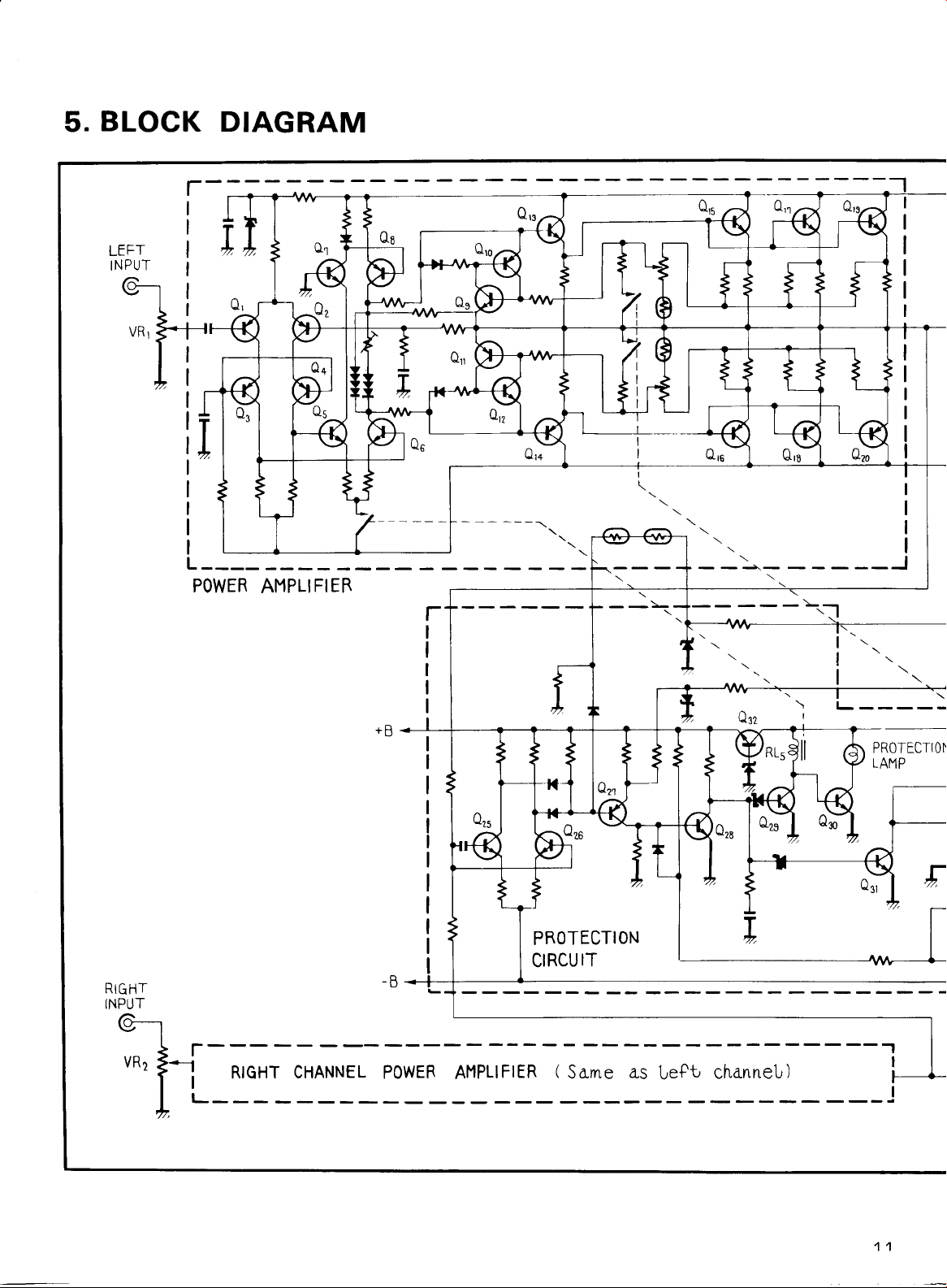
BLOCK
5.
DIAGRAM
LEFT
TNPUT
etl
u*,il-
Li
I
I
POWER
AMPLIFIER
_
--
--_\
Qlr
I
RIGHT
INPUT
@-9_l
u*t
: l---
f*l
'l
ll
Irl
tl
LE--
RIGHT CHANNEL
powER
PROTECTION
CIRCUIT
(
AMPLTFTER
same
as
Lelt,
t
-----r
cirannel,,)
PROTECTIOI
LANP
I
44
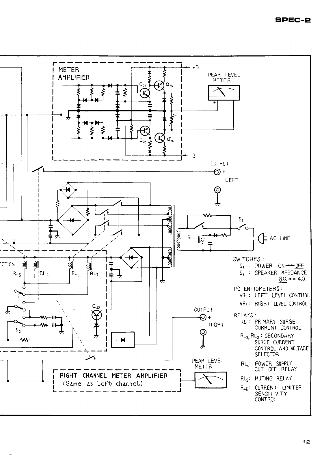
Page 12
t-
METER
ANPLIFIER
PEAK
METE
OUTPUT
LEVEL
R
L
EFT
sPEC-e
-
t--
aRrcHT
(Sarne
|
\
CHANNEL METER
I
AllPLtFtER
as Left, channeL)
!
TPUT
@+
6\-
+
LEVEL
PEAK
METER
1
RIGH
AC LINE
SWITCHES
Sr : P0WER
Sz . SPEAKER
POTENTIOMETERS
VRr
VR2: RIGHT
RELAYS
RL1:
RL2, RLs
RLn:
RL5:
Rh' CURRENT LIM{TER
:
0N*_0EF
I|'lPEDANCE
8.0*
:
:
LEFT
LEVEL C0NTR0L
LEVEL C0I{TR0L
;
PRIMARY
CURRENT
:
SURGE
CONTROL AND VOLTAGE
SELECTOR
P0WER
CUT_ OFF
MUTING
SENSITIVITY
CONTROL
SURGE
CONTROL
SECSNDARY
CURRENT
SUPPLY
RELAY
RELAY
4Q,
t<
Page 13
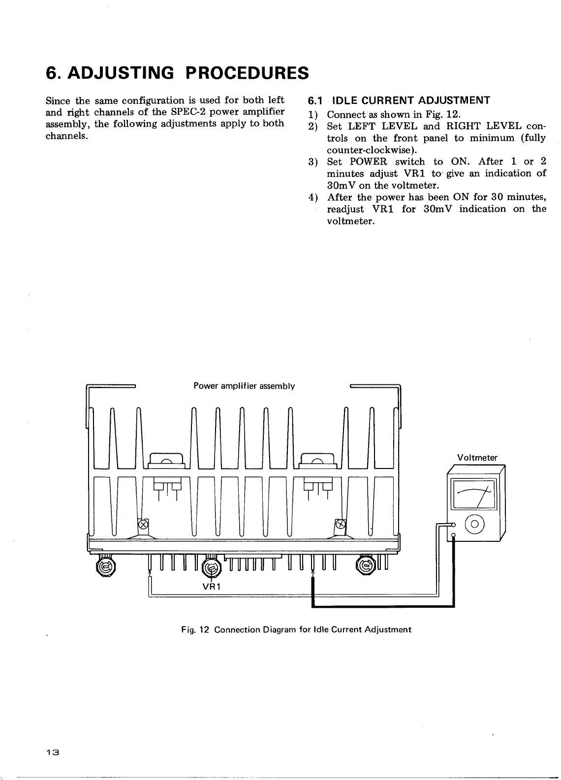
ADJUSTING PROCEDURES
6.
Since
the
right channels
and
assembly,
channels.
same configuration
of
the following
SPEC-2
the
adjustments
used for both
is
power
apply to
Power
amplifier
left
amplifier
both
assembly
IDLE
6.1
1)
Connect as
2)
Set LEFT
trols
counter-clockwise).
Set
3)
minutes adjust
30mV on the
After
4)
readjust
voltmeter.
CURRENT
on
the
POWER
the
VRl for 30mV
shown in
LEVEL
front
switch to
VR1
voltmeter.
po\Mer
has
ADJUSTMENT
Fig. 12.
and
panel
to
been
RIGHT
to
ON.
give
ON for 30
LEVEL con-
minimum
After I or
indication of
an
indication on the
(fully
2
minutes,
13
Fig. 12
Connection
Diagram
for
ldle
Current
Adjustment
Page 14
6.2 CURRENT
ADJUSTMENT
Note:
The high
dummy
200W
8S},
output
load of 4O
dummy
100W
loads in
load is
LIMITER
power
of the
and more
not available,
parallel.
SENSITIVITY
SPEC-2
requires
than 200W.
connect
If
two
Connect as shown
1)
Set SPEC-2 impedance selector switch to
2)
(even
though a
a
a
VR2
While
3)
the
In
the same manner, adjust VR3
torted
voltmeter
the
just
to
waveform.
point
in Fig. 14.
4O
dummy
indicated
distorted
the lower
load is used).
point
the
half
with
30V/(40
upper half of
to
28.3V/(44).
adjust
),
just
8O
dis-
ilPur
|
/
la
AF
Fig.
13
signal
The Position
generator
of VR2
Voltmeter
and VR3
VR3
Osilloscope
ooo
Waveform
Fig.
14
Connection
Diagram for
Current Limiter
Sensitivity
Adjustment
Page 15
6.3
1)
2)
3)
METER
Connect
Adjust
44.7V
At
is for
on
as shown
input
on
this time,
right channel) for
LEVEL
the
AMPLI FIER
Fig.
in
level
to
voltmeter.
the
adjust VR1
meter.
ADJUSTMENT
16.
give
an indication
(left
channel;
(250W)
OdB
indication
Meter
SPEG.E!
of
VR2
amplifier assembly
Fis. 15
SPEC-2
NPUT
I
r
IA
R
Position of
The
VR2
VR 1
VR2
and
RIGHT
AF.
VRl
Voltmeter
.----.
S
Fig.
a
att\
'J-'
16
Connection Diagram for Meter
Amplifier Adjustment
15
Page 16

7. DISASSEMBLY
1. Removing the Top Cover
Remove
cover.
L2 screws
t],:.e
(A)
to
detach
the top
2. Removing the Bottom
Remove
13 screws
the
plate.
Plate
(B)
to
(A)
E
@
,a/-*rutez&tt"-..^
""*€:
"€a*...
i
detach the
(A)
n
bottom
?soo
ToP
(A)
9
cover
(A)
Y
*""'-€(A,
.- -
A)
I
g
-
\
-.
""",:'i,*u*
Page 17

sPEC-e
3. Removing the
(1)
Remove
out.
(2)
Remove
LEVEL shaft
(3)
Remove
main body.
removal.
the
Front
all
the
panel
Front Panel
control
nuts
4 screws
The front
knobs
LEFT LEVEL
and washers.
(C)
by
each
on
panel
pulling
and
is ready for
them
RIGHT
side of the
'--=-
-..----
)
,/.
7
-'-
.
Washer
j
@(c)
Main
body
17
Page 18

4. Removing the
(1)
Remove
the top cover, bottom
panel.
(2)
Unscrew
the 4 screws
stay.
(3)
Unscrew
printed
This
moved,
length
the 4 screws
circuit
allows
though the
lts
of
Meter Amplifier
(D).
(E)
board on
printed
the
peak
circuit board
distance
lead wire.
Assembly
plate
and
Remove
the
which mount
level
meter.
is limited by
front
panel
the
be
to
the
Meter amplif ier assembly
Panel
stay
Page 19

5.
Removing
(1)
Remove
(2)
Unscrew
power
(3)
Unscrew
printed
Power Amplifier Assembly
the
the
top cover
the 4 screws
and bottom
(F)
which mount
plate.
amplifier assembly on the rear
the 4 screws
circuit board
(G)
on the
which mount the
heat
sink.
SFEC.A
the
panel.
Printed
circuit board
Heat sink
19
Page 20

PARTS
8.
1.
Top
View
LOCATIONS
Power
amplifier
assembly
{RIGHT CHANNEL)
AWH-045
Power
supply
circuit
assembly
AWR.093
Electrolytic
r 5,00&F
ACH-052
capacitor
100v
Power
amplitier
assembly
(LEFT
AWH-045
CHANNEL}
Oiode
KBH2504
Power
transformer
ArT-245
Meter
amplif ier
assembly
AWM.081
Page 21

siPEc-e
2. Front Panel
Front
3.
View
View
with Panel
Handle
ANK,O84
Knob
(POWER)
AAD-109
Removed
Front panel
ANB,358
assembly
'm
K nob
(LEFT
AAB,097
Knob
(R
IGHT
AAB-097
LEVEL)
8:
&E
LEVE
L)
Hand
le
ANK.O84
(bar
Lamp
8V 0.3A
AE
L-058
switch
Lever
(POWER)
ASK.OSO
type)
Peak level meter
(LE
FT CHANNEL)
AAW,O51
with wire
Lamp
8V 50mA
(PROTECTTON
AEL-O42
)
Peak
level
(R
IGHT
AAW.O51
CHANNE
Variable
100ko-B
(LEFT
ACV-009
meter
LEVEL)
Variable resistor
100kf,-B
(R
IG HT LEV E L)
ACV-009
L)
resistor
Page 22

4. Rear View
Input
AKB.O13
terminal
Output terminal
AKE.02O
(A)
Spacer
AEB.O75
Spacer
AEB.075
Qround
terminal
AKE.O19
Slide
switch
(IMPEDANCE)
ASH.014
Output
AKE.O21
terminal
(B)
Page 23

ir3
EXPLODED
9.
NOTE:
Parts
indicated in
green
Top
ANE.097
VIFWS
type cannot htisupplied.
BM.3x8*,
cover
ili
BM.3x8
PM.4x10
BM.3xg
rTw.30
PM.4x10
@.
rTW.3d
d
@''
-(9-
:ii!i:.ii1iitiiil,i,r::.iiirf
Front
ANB.358
Handle
ANK-084
illliliJtlirj.l$;t;:1}?;i!,Y,
(POWER)
Knob
AAD.109
Knob
(LEFT
AAB-097
LEVEL,
PM.3x8
FW.3@x0.5t
panel
assembly
RIGHT
{ii'i!.!tir.1
1i1r1;tl,iii!:il
VEL)LE
@
iri
:
PART
1
PM.3x8
FW'3@x
0.51
@^
Nut
871-004
Spacer 9dx1t
M9
M45-086
3
Page 24

sIrEc-e
PART
page
S*e
3
27
PM.4x
RT.4x16
Foot
assembly
AEC.178
RT'4x16
10
30
,r..",
i
*'b
BM'3x8
Foot
assembly
AEC-178
RT'4x
16itTW
Page 25

PART
1
NOTE:
Parts indicated in
green
type cannot
..
supplied.
tb
t.'1
,i::,
Metpf
amplifier
AWM-081
assembly
A
B
r..
-i
,i
.
RT'3x6
(bar
Lamp
AEL-058
:ffi
type)
qgf.l:,.,,,,i,,
PL
socket
AKK-OO2
-:iii:i:r
.'
ii
i-:.fl.ira:
8V,
..PL
r,
:,,
Relay
ASR.O15
N.3d
PM.4x
8
orw.ao'
A
B
c
D
25
Rubber
AEB-051
Lamp
with
AEL.O42
holder
wire
8V,
c
D
50mA
3
Page 26

PART
NOTE:
Parts indicated
Power
2
green
in
transformer
type cannot
ATT-249.
A
':.:i.!,:itlii:!'1.:i.i..!1j,..:1i.i-1:.:t:;i,|:'it,r'.:.i,.tft:itjiri:rl:lilsi
I
B
Electrolytic
15,000pF, 100V
ACH-052
E
15,000pF
ACH-052
PM'4x10
capaci
lectrolytic
Diode
KBH-2504
ti'r
supplied.
be
Power
AWR-093
T'4x8
supply
RT.4x8
RT.4x16
circu
it assembly
Fus6.2A
AEK;103
RT'4x8
3
.,1
"i
Fuse 1
AEK-1I
B
Ceramic
0.01pF, 1
ACG-00!
c
RT
c
Electrolytic
15,0001rF,
t00V
ACH-052
Spring
washer
ABE-026
Nut
M6
Spring
washer
ABE.026
Nut
M6
ABN.O17
M6
MG
sw.30
Mounting pillar
ALA.O21
Terminal
D
striP
1
(4P)
PM.3x8
RT.3x6
D
PM.4x10
26
Page 27

siPEC-e
PART
NOTE:
Parts indicated in
A
Terminal 9o.16
AEC-252
Terminal
M4e-052
B I
Terminal
M49-014
Slide switch
ASH-014
c
3
green
Output terminal
AKE.O2O
Output
AKE_021
board held metal
held
board
(IMPEDANCE)
metal
type
cannot
(A)
terminal
,lil
be
(B)
t
L
Sonnector
i$sembly
6DX-020
supplied.
(6P)
power
ACp
ADG
ry''
-
cord
-013
BM.3x8
OTW'4d
wN.4O
,,tt
tinBUi$i;il.rh;l.i'.:,
AKB-013
Ground
AKE.O19
terminal
Screw
ABA.O89
Spacer
AEB-075
i
A
:
c
D
Connector
assembly
ADX.O23
Power
amplifier
AWH.O45
(See
page
(3P)
28)
assembly
Connector
ADX-024
conn$to,
assernhly
(6P)
ADXS21
a*sembly
,!i
PoweF.ampl
AWH€45
(See
p$se
if ier
28)
lr
(3P)
assembly
Connector
assembly
ADX-O22
(5P)
Connector
assembly
ADX-O22
(5P)
D
Page 28

POWER
AMPLIFIER
NOTE:
Parts indicated
green
in
ASSEMBLY
ype
t
cannot
be supplied
A
B
RT.3x
Varistor
,STV4H
BM.3x8
A
BM.3x10
Toggle
nut
AEC-225
.t'..ii.:.:t,lt':',
,::.,r'.:f
Power
2SC1
.i11:.:..:.,.r:rii...:.ljt::ri.lf,iL:,:llt!r.il!tr...,.,ft,...ii.:,:
i
i::rti..ii
rr,i:
transistor
586
Power
transistor
2SA909
PM.3x
16
B
8
,
I
Insulating
wafer
x:c-076
c
Transistor
AKH-OO1
BM.3x8
'
Contact strip
AKM-018
BM'3x8
' '
,"Contact
:1.
',
l'
strip
'.
AKM.O19
D D
(3P)
,'.
i:'
(5P)
socket
Contact
AKM.O2O
strip
(6P)
BM.3x
8
c
2e
Page 29

sPEC-e
NOMENCLATURE
The fouowing symbols
Symbol
RT
PT Pan
BT Binding head
CT
TT
ocT
CM
octv
Erazier
head tapping
Countersunk head tapping
Truss head tapping screw
Oval countersunk head
Pan
head machine
Countersunk
Oval countersunk
OF SCREWS.
Do.cription
head tapping
tapping screw
head
WASHERS ANDNUTS
stand for screws,
screw
screw
screw
tapping
screw
machine
head
washers and
Shspe
fF-
ft-.
u--
t-
@
vt-:t
F
nuts as shown in exploded view.
Symbol
EW
SW
N
oTw
E type
Spring lock
Washer
Internal toothed lock
Outernal
sc Slotted set screw
Slotted set screw
Dsscriprion
washer
faced
nut
toothed lock
washer
{Cone
(Flar
washer
ooinr)
point)
Shape
\D
oil
A4
\\,
og
@fl
@il
#l
e=D
cEr
I
Tt!!
AM
PSA
PSB
PSF
EXAMPLE
PM ' 3x8
-::::";::1,,
L
Truss head
Binding head
Pan head
Pan
lock
Pan head
screw with sprjng
head
screw
washer
scr6w with flat
Symbol
machine screw
machino screw
with spring
and flat
washer
washe.
r
G=
hr
HS
ocw
CW Countersunk head
FW'9@x 1'
Hexagon socket headless
Oval
countersunk
Round head wood screw
T-
th;skns55
-
diameter
Symbol
set
head
wood
wood screw
in mm ( I
(
in mm
d
@@
)
)
-11'
/At
{( )l d
I
Page 30

1O. SCHEMATIC
DIAGRAMS, P.C.
AND PARTS LIST
BOARD PATTERNS
10.1 SCHEMATIC DIAGRAM AND MISCELLANEOUS
Miscellaneous Parts
CAPACITORS
Symbol
c1
c2
c3
c4
c6
c7
c9
c10
RESISTORS
Symbol Ds3cription
R1
VR2
SWITCHES
Symbol Description
s1
Csramic 0.01 150V
Electrolytic
Electrolytic 15,OOO
Electrolvtic 15,000
El€ctrolytic
Ceramic 0.O1 150V
Ceramic
Ceramic
Ceramic O.O1 150V
Ceramic
AND POTENTIOMETEBS
Metal
Metal
Variable resistor
(LEFT
Variable
(RIGHT
(POWER)
Slide switch
(IMPEDANCE)
List
D€scription Parl No.
15.000 |OoV
15,000 l00V
O.Ol 15OV
O.O1 15OV
0.01
oxid6 4.7k
oxide
LEVEL)
4.7k 3W
1ook-B
resistor 100k-B
LEVEL}
IOoV
1oOV
'l50V
3W
ACG-003
ACH-052
ACH-052
ACH-052
ACH-052
ACG-001
ACG-001
ACG-001
ACG-001
ACG-003
RS3P
R53P
ACV-009
ACV-009
ASK-O80
ASH-014
Part
No.
472K
472K
Part No.
PARTS
NOTE:
.
Copocitors: in
.
fiesrsao/s. in a, AW unless otheruise
FUSES
Symbol
FUl
FU2
FU3
FU4
FU5
FU6
FU1
FU8
OTHERS
Symbol
T1
PL1
PL2
PL3
PL4
PL5
RL1
RL4
D1
D2
pF
unless
otherwise noted
D€scription Part
Fuse
Fuse
Fuse 1A
Fuse
Fuse
Fuse 12A
Power
Lamp with wire 8V, sOmA
Lamp
Lamp
Lamp
Lamp
Relay
Diode
Diode
(Secondary)
2A
(Secondary)
2A
(Secondary)
(Secondary)
1A
24
{Secondary)
(Primary
D€rcription Psrt
transformer
(bar
lbar
(bar
(bar
l
typel 8V,
lype) 8V, 0.3A
rypel 8V, 0.3A
typel
0.3A
8V, 0.3A
p:pF
noted h:hf]-, M:Ma
No.
A E K-103
AE
K.103
AEK.106
AE K"106
AEK-103
AEK-301
No,
ATT.249
AEL.U2
AEL-O58
AE L-O58
AEL.O58
AE L-O58
ASR-015
ASR-016
KBH-2504
st801-02
2sA7s8
25A725
2SC1312
Bt
g7Y-ct
E itsE,
-82
r--r
ffiirE"
U)-B
2sA733
2sA872A
2SC94S
2S8507
2SB63OA
2SD31 3
2SD61OA
2SA909
A--B
4J-;
(2s8600A)
2sc1586
(2SD555A)
|lF}r
l/11 lr{ -
c
U l$=%
'-'-l'>B @?
2sc1384
rlPl\
[ \l 5,t
\\sl
c
-
Page 31

Schematic
Diagram
nNe Ass)
PO$/ER
AwH
-
04$
INPI.JT
LCF
| tr\/trt
@
I
TI
t;
rt
CONTROL
0r.Qe,
2SD6l0A
2
l
r0
Qrz
'+
c?60P
C3
n,
.1;=
16s
|
20v
,'9
tH o,,Dr,Ds,os,Dr,Dro
POWER
lS24?3
xs
N1P
ASSy
AWH - 045
2SA?33
0r,o"
os,q'o2SC945
xt
xz
&:22
Rr ^
2SCt58S'xi
rER
AtlP
orDgz
or,Qr,Qr,Qr2SC13l2,c
r'nt:ilrlir:,+il::.]
e:,er,0s,0c
RrlK(2'\i)
Assy
lS24?3x3t
iriir.t
;i:ri,
rj:,
2SA?25'+
Awll-081
:nji.:.iir!
Drs
:Fil-,u
6
E
d
.:i+
6
i
:
NOTES
S W I TCHES
:
P0$/ER
Sr
SPEAKER
ST,
+
0N
8(}-4Q
0,,l524?3
SWITCH
oFF
II'IPEDANCE
flss 2.'lK
wZiS?
ll'.25850
j
0n*
RELAYS
RLr
RLr r
RL+
RLs
3
3'l
Page 32

ri
Cl58*xi
LEFT
RIqHT
050
9N
PO9{ER $'mY ASSy
rs:
t6T
i$
---
A
A
AWR
-
093
sPEC-e
RELAYS
RLI PRII'4ARY
CONTROL
RLz.3
SECONOARY SURGE
CONTROL ANO VOLTAGE
OUTPUT
RL+
NUTING
RLs
kto^s
SURGE
RELAY
CUT-OFF
RELAY
Rs. ??
CURRENT
CURRENT
SELECTOR
RELAY
RELAYS
RLr
c'URRENT
CONTROL RELAY
AC r20V
50-60 Hr
LIilITOR
SENSITIVITY
'
l-l]
:
v
(
:
v)
v0tTAGE NECESSARY
SIGNAL
250fv,/6Q
DC
OC
DC CURREN.T'
oUTPUT
NO INPUT
VOLTASE
VOLTA$S AT 25OfV/EQ
AT
::i;l
NO
AT
POWER
INPUT
FOR
(lKHz)'
SIGNAL.
OUTPUT
SIGNAL,
OBTAINING
POWER
32
Page 33

10.2 FOWER
SUPPLY CIRCUIT ASSEMBLY
(AWR.Og3I
Power
Por,ver
Power
transformer
transformer
Power
transformer
(OR)
(O
R
)
transformer
ED}
{R
(R
EO)
Cz- Cs
15,000/1(xh4
Rr,Rz
4.7ksl(3W)
Power
amplifier assembly-No.21
Meter amplif
ier assembly-No.23
Power amplif ier ass€mbly-No.5
Meter
amplif
ier
assembly-No.7
Page 34

Power
transformer
transformer
(GRN)
(GRN)
transformer
transformer
(BLK)
(GRY)
transformer
transformer
(BLU)
Power
amplifier
amplifier
Meter amplif ier
ampl itier assembly-No.5
ier assembly-No.7
amplif
amplif ier ass6mbly-No.
amplifier
amplifier
ass€mbly-No.10
ass€mbly-No.
ass€mbly-No.6
6embty-No.6
1 1
ramps
8V 0.3Ax4
assembly-No.5
(R
CH.)
(L
CH.)
Page 35

Page 36

Parts
List of Power
CAPACITORS
Symbol
c1
c4
Ceramic
C€ramic
Ceramic
Ceramic
C6ramic
Supply Circuit
De3cription
o.01
o.o'l
0.01
0.01
0.01
Assembly
150V
150V
150V
150V
150V
(AWR-093)
Psrt
No.
ACG-O04-0
ACG-004-0
acG-00+o
ACG-004-0
ACG-004-0
sPEC-e
c6
c7
c8
C€ramic
C€ramic
Ceramic
c9
cl0
cl1
c12
Efoctrolytic
Electrolytic
RESISTORS
Symbol
R1
D€.cription
SEMICONDUCTORS
Sytnbol
ol
D2
D3
D4
D6
o7
DA
D9
D10
Diod€
Diode
Diode
Diode
Diode
Diods
Diode
Diode
Diode
Diod€
Oe.cription
0.01
0.01
0.ol
47O
1000
20
20
150V
150V
150V
35V
35V
201,
2w,t
ACG-OO4-0
ACG-O04-0
t:::"""
cEA
471P35€5C
cEA 102P35-85C
Prrt No"
ACN-00S0
ACN-005-0
Pr.l
No,
-04
stB0l
st
801-o4
srB01-04
-04
stB0l
sl Bot-02
slBol-o2
srB01-02
slaol-o2
stB0l-02
stB01-o2
OTHERS
qmbol
RL1
RL2
Rolsy
Rolay
Ds.cription
Part No.
ASR-013-O
ASR-O13-0
Page 37

IO.3
POWER
AMPLIFIER ASSEMBLY
(AWH.I!4sI
Meter amplif
Polwr
supply circuit s€mb|y.Nos.23,24,25
Pn-Cr3
25A90
assembly'No.24
i€r
9
MEtsr amplif ier asembly-No.21
Power
amplifier ass€mbly.No.7
(221
(R
CH.)
Meter
amplitier assembly-No. 18
(
191
Power srpply circuit assembly-N06. 32,31,34
ier
smplif
ass€mbly-No.7
Pourer supply circuit Nernbly-No.28
Page 38

Meter amplifisr
Metor amplif ier
Power supply circuit
assembly-No. 15( 1
assembly-No.23
ass€mbly-N
6)
06.
19,
20,21
0*-
0,r
25C1586
VRr
100k-B
Page 39

siPEc-e
=
mU
f
d
c{
G
(M9)s'0
-(\l
fr
-rC)
dF
t---
F
0'u
A
&-l
ffi
(/.tS)Sn
.^6
jitn
jg
@(v
(o
A
B
r
i*
!o
tlt
r
(D
(M?l)Offuu
$l
<n
<\l
/+
l3
=
.'4i
uL:t
iE/-ZZel
ilzu
-
t'0
6l
c
0i0tu
N
o
o
ct
.;<
-^./t
5c\r
N
C-l
E*
G'
f
r
=
F
"EE
(o
ct
.J'
(!
y8:tsu
l*
)1,9
sg
e
e
o9o'o''
a
(?)
r
sr
cl
ct)
D
d-
c
td
<a> -at)
- O-.o
=
a
F
t
+c?
)001t'u
ol
9A/
riil;*ri:l;
s-
.t>
4
t
o
o
*'$
"'
vsttu
?
E
di+
cl
D
dI;
r
y0
Y
ry
t_
N
tlzz'u
39
Page 40

Parts
List of Power Amplif ier Assembly
(AWH-045)
CAPACITORS
Symbol Description
c1
c2
c3
c4
c6
c8
c9
c10
Efectrolytic
C€ramic
Ceramic 47p
Electrolytic
Electrolytic 10
Efectrolytic
Ceramic
tulylar
lvlylar
Ceramic 47Op
ct1
:::T::
c13
cl4
c15
cl6
c18
RESISTORS
R1
R3
R4
R6
R8
R9
R10
Ceramic
C6ramic
Ceramic 820p
Ceramic
AND POTENTIOMETERS
4.7 35V
68p sOV
10 35V
22 35V
4p 50V
0.1 20OV
0.1 200V
470p
O.O47 l50V
22p
47Op
2.2M
'110k
2.2k
15k
1.8k
r.8k
33k
't5k
4.7k
4.7k
50V
35V
500V
500v
50V
50V
50
Part No.
cszA 4R7M
35
Symbol D6scription Part
ccDsL 680K 50
ccDSL 470K
50
cEA t00P 50
r00P
cEA
cEA
220P
35
35
ccDsl o40K 50
104K
coMA
200
coMA 104K 200
CKDYB
:.:?L'.1""
ACG-OO9-O
CKDYB 220 50
CKDYB
CKDYB 471K
RDY.PS
RD%PS 114J
RD%PS
RD7.PS
ROlr'rPSF
ROIZPSF
RD7.PS
RDz.PS 153J
RS2P 472K
ROy.PS 472J
471K 5OO
"'
821K 50
50
225J
222J
153J
122J
122J
333J
SEMICONDUCTORS
R31
R32
R33
R34
R35
R36
R37
R38
R39
R40
R41
R42
R43
R44
R45
R46
R47
848
R51
vR2
VR3
Symbol
o1
o3
04
o5
film
C6rbon
film
Carbon
film
C€rbon
film
C€rbon
film
Carbon
lilm
Carbon
film
Carbon
tilm
Carbon
Wire wound
Wire wound 0.5
Wire wound
Wire wound 0.5
Metal
oxide
Wir6 wound 2.2
Wire wound
Carbon film
film
Carbon
Semi-fixed
Semi-fixed
S6mi-fixEd
Transistor
Transistor
Transistor
Transistor
Transistor
27
27
10
10
10
10
10
10
0.5 5W
0.5
0.5
lk
1O
910
1.3k
470-B
100-B
100"8
Doscription Part No.
5W
5W
5W
5W
5W
3W
vll
5W
No,
RD%PS 27OJ
RD%PS 27OJ
RDY.PS 1OOJ
RDY.PS l
RD%PS 1OOJ
RD%PS 1OOJ
RD%PS l
RD%PS I OOJ
RTSB
RTsB OR5K
RTsB OR5K
RTsB
RT5B OR5K
RTsB
RS3P 102K
RT2B 2R2K
RTSB 1OOK
RD%PS 9'I1J
RDY.PS
ACP-051.o
ACP-050-0
ACP-050-0
2SA798-G or F
2SA872A-D or E
2SA872A-D or E
2SD61oA-R
2SD6'l0A-R
OOJ
OOJ
ORSK
OR5K
ORSK
'I32J
or S, O
or
S, O
40
R11
R12
R13
R14
Rt5
R16
Rt7
R18
R19
R20
R21
823
F24
100
100
100
100
22
't
10k
22
22
Carbon film
.Carbon film
Carbon lilm
Carbon filrn 22Ok
film
Carbon
1ook
100k
22Ok
47
RD%PMF lOIJ
RD%PMF 101J
RD/,PMF 101J
RD%PMF 101J
ao%PsF 22oJ
RDT.PSF
BDT.PSF
BD%PSF
RD7.PSF 22OJ
RD7.PS
RD%PS 101J
AD%PSF 221J
RO%PSF
RD7.PS
RD'/.PS
RD%PMF
RDT,PMF
RD7.PS
RD%PS
22OJ
114J
220.J
1O1J
221
47OJ
470J
471J
471J
331J
331J
06
Q7
08
o9
010
011
012
or3
014
015
o16
o17
018
019
Transistor
Trantastor
Transistor
Transistor
Transistor
Transistor
Transistor
Transistor
Tlansistor
Transistor
Transistor
Transistor
Transistor
Transistor
2SD61OA-R
2SB63OA-R or S, O
2SA733-R
25C945-R
25C945-R
25A733-R
25061oA-R
2SB630A-R
2SC1586-0 or
25D555A-R
2SC1586-0
25D555A-R or
2SC1586-0 or
2SD555A-R or S
2SA909-O
2S8600A-R or S
2SA909-O or R
2SB60OA-R or S
2SA909-O
2S860OA-R or
or S, O
or S, O
or
or
or R
or R
or R
S, O
R
S
S
R
S
Page 41

€tPEC-P
Symbol
o1
D3
04
D5
D6
o7
D8
o9
010
Dl1
Thl
Th2
Th3
OTHERS
Symbol
L1
D€scription
Zener diode
Diode
Diode
Diode
Diode
Diode
Diod€
Diode
Thermistor
Thermistor
P.T.C.
thermistor
D.3criplion
AF choke coil
Part No.
BZ
340
1S2473
(1S1555)
STV3H-Y
1S2473
(1S1555)
152473
{1S1555)
-04
stB0l
stB01-04
152413
{1S1555}
1S2473
(1515551
STV4H
TH101-2
TH101-2
AEX-O44
No.
P.rl
ATH-012-0
RLl
RL2
Reod
Reod
relay
relay
ASR-017-0
ASR-005-C
Page 42

A
B
10.4
METER AMPLIFIER ASSEMBLY
(|YlD00ereu
t-
raN
<?
(?
o
a,
(\l
c
a
(Mzll)vq
0su
Jyl .
i-k$ 5
F.o==
+t
/Za
9t
t0'0
r
'- -
o(.,d-3
dtr
+
({
U,
So
r_\-
9c/01
31.')
-1r)
DtJ
zLJ
.tO
r
|l
*
G
(n
ql
cD
6r,
ro
{
q)
c)
U'
(\l
a
9
N
PE
,=
+=
(J
6l
(t)
::(n
-Gl
-
CJ
x
(?
r
.f
<\r
I
,..: ,r{til:
x
GT
r
P(!-)
dF
-(J
ur
-2
(NWM.O8l}
(M%)vi
sc/01
r
o
ro
m
(t,
cl
=
<i
Ll.
Jlo
sc/zlst)
!n
T
<0
o
N
=
.O
sr/
]Lv
C-
N
=
',
/ c7*
8;
s*
2
+N
t,
OO
N
(\l
o
I
,o
GO
.4
c-l
t
A
--
T
>.Ll
<
co
<f)
zz
esu
(?
t!*,
t
al
?
yOgi
rsu
B
$
o
I
o
@
(t,
N
o
tfj
#t
J\tta
1'-t_
I
4?
-00r
g
c
0:,!'^'l
A i ._ i
st
v
X
K)
s:
cr
s2
C)
U'
ct,
6r
cr
s
c!.
c:
a
q
ct
€
N
c-)
r
F$
=
D
S
E
o<\l
rl
.t,
I
c-
+
CT
ygtzz
u
g.
ct
";
o
j
a
C'
zu^
c
5toslscu
ystrzu
D
Page 43

Peak
le\rel meter
(R
chl
-+*---.-------<',
r,
,,,
*
{ia"!i;
tff
t.
E
*"
l''
:':'l
i{
15
Power
amplifier
Power
amplifier
amplifier
Power
supply
amplifier
Power
supply
Power supply cirbuit
Power supply circuit assembly-No.30
Power
amplifier
Power
amplifier
assembly-No.8
assembly-No.8
assembly-No.2
circuit
assembly-Nos.
assembly-No. t6
circuit assembly-Nos.
assembly-No.31
assembly-No.4
assembty-No.4
(L
{R
l
23, 24, 25
(R
CH.)
{L
CH.)
CH.)
19.20,21
<---'------------
CH.}
8r,
4f,,
-"
Su
8s,
4f,
Power amplif ier assembly-No.
Power amplifier
assembly-No.19
43
{R
l9
CH.)
Page 44

Peak
E|FEC-P
lar6l
meter
(L
ch)
rNo.19
r(R
CH.)
(L
CH.)
Power
amplif
Power supply
Power
supply circuit assembly.No.26
circuit assembly-No.27
Power
transformer
Power
transformer
Power
supply circuit assembly-No.35
{BRN}
(WHT)
supply circuit assembly-Nos.32,33,34
ier assembly-No.5
Page 45

Parts List of Meter Amplif ier Assembly
CAPACITORS
Symbol
c1
c4
c1
c8
c9
cl0
c11
c12
cl3
c14
cl5
cl6
c18
c19
c20
c21
RESISTORS
Electrolytic
Electrolytic
Electrolytic
Electrolytic
Electrolytic
Efectrolytic
Efectrolytic
Efectrolytic
Efectrolytic
Efoctrolytic
Efectrolytic
Ceramic
Ceramic
Ef€ctrolytic
Efectrolylic
Electrolytic
Electrolytic
::
Electrolytic
Electrolytic
AND POTENTIOMETERS
Symbol
M6tal oxide
Metal
R3
R4
R8
R9
Rr0
R1l
F12
R13
Rl4
R15
R16
R17
R18
R19
R20
R21
R22
R23
R24
R25
Carbon
Carbon film
Carbon
Carbon film
Carbon
Carbon film
Carbon film
Carbon
Carbon film
C€rbon film
Carbon
Carbon film
Carbon film
Carbon
Carbon film 4.7M
Carbon
Carbon
C€rbon film 4.7M
Carbon film 15k
Carbon film
Carbon
Carbon film 15k
Carbon
Description
1 25V
1
25V
1 25V
"..
1
220
22O
220
22O
47O
47O
47O
0.O1
O.01
22
22
10
10
10
10
10
25V
6V
6V
6V
6V
6V
16V
50v
50v
35V
35V
35V
35V
160V
35V
35V
D€scription P6rt
1k 2W
oxide
film
lk 2W
47k
47k
film
film
filrn
film
film
film
film
film
film
8.2k
8.2k
8.2k
8.2k
'l
OO
10O
10O
1O0
27
27
27
2'l
4.7M
4,1M
15k
15k
3.3k
cszA
cszA 0't0M 25
cszA
cszA
cEA 221P
cEA 221P
cEA
cEA
cEA
cEA
cEA
cKoYB 103K
CKDYB
cEA 220P
cEA 220P
cEA r
cEA 1
ACH-313-O
cEA 100P
cEA t00P
RS2P
RS2P
RD%PS 473J
RD%PS
RD%PS
RD%PS
RD%PS A22J
RD%PS
RD%PS
RDy.PS 101J
RD'/.PS 101J
RD%PS 101J
RD%PS
RD7.PS
RD/.PS
RD'/.PS 270J
RDl.PS
RD%PS 475J
RD7.PS 475J
RDY.PS
RDI.PS
RDY.PS 153J
RD7.PS 153J
RD7.PS 153J
RD7.PS
(AWM-081
Pert No.
)
010M 25
or0M 25
01otvr 25
6
6
221P
6
221P
6
471P
6
471P
6
471P 16
50
1O3K 50
35
35
00P 35
00P 35
35
35
No.
't02J
102J
473J
822J
822J
822J
101J
27OJ
27OJ
27OJ
475J
475J
153J
332J
Sylhbol
R27
R2a
R29
R30
R31
R32
R33
R34
R35
R36
R37
R38
R39
R40
R41
R42
R43
R44
R45
R46
F47
R48
R49
R50
R51
R52
R53
R54
R56
R57
R58
R59
R60
R61
R62
R63
R64
R65
R66
R67
R68
R69
R70
VR1
VR2
De.cription P€rt
Carbon film
Carbon film
film
Carbon
film
Carbon
film
Carbon
film
Carbon
film
Carbon
film
Carbon
film
Carbon
film
Carbon
film
Carbon
Iilm
Carbon
Carbon film
lilm
Carbon
3.3k
3.3k
3.3k
3.3k
3.3k
3.3k
3.3k
150
150
150
l50
330
33O
4.7k
Carbon film 1.5k
lilm
Carbon
Carbon
Carbon
tilm
tilm 100
6.8k
6.8k
Carbon tilm 100
film
Carbon
8.2k
Carbon filrn 150k
film
Carbon
Carbon
Carbon
Carbon
Carbon
filrn
tilm
tilm
lilm 22
4.7k
15k
15k
'lsk
Carbon film 150k
Iilm
Carbon
tilm
Carbon
Carbon film
film
Carbon
film
Carbon
tilm
Carbon
{ilm 15k
Carbon
tilm
Carbon
Metal oxide
film 1k
Carbon
4.7k
2.7k
2.2k
47k
4.7k
15k
k
I
330
Carbon film 22
Carbon film 22
Wire wound 4.7
Metal oxide
Carbon tilm
film
Carbon
Semi-fixed
Semi-tixed
1k
47O
47O
100-B
100-B
hw
vzw
1AW
vd
1AW
5W
2W
No.
RD%PS
RDY.PS
RDY.PS
RD/.PS
RD7.PS
RD/.PS
332J
332J
332J
332J
332J
332J
RDY.PS 332J
RD%PS 151J
RDY.PS
151J
RDI.PS 151J
:?':::1"'
RD'/.PS 33I J
RO%PS 331J
RO%PS 472J
RD/.PS 152J
RD%PS
RD%PS
RO%PS 101J
RD%PS 101J
RDy.PS 822J
RD%PS 154J
RD%Ps 472J
RDY.PS 153J
RD/.PS |53J
RO%PS 153J
RD%PS 22OJ
RD7.PS
RD%PS 472J
RO%?S 272J
RD%PS 222J
RDY.PS
RO%PS 472J
RD%PM
RDY2PM 153J
RD7,PM 1O2J
RS2P
RD%PM 1O2J
RD%PS 22OJ
RD%PS 22OJ
RT5B 4R7K
RS2P
RD%PS 471J
RD7.PS 471J
ACP-O50-O
ACP-050-0
682J
682J
154J
473J
.I53J
331J
102J
45
Page 46

SEMICONDUCTORS
Symbol
o1
a2
o3
04
o7
08
09
010
011
o12
013
014
015
Transistor
T€nsistor
Transistor
Transistor
Transistor
Traosistor
Transistor
Transiator
Transistor
Transistor
Transistor
Tranaistor
Transistor
Transirtor
Transistor
Doscription
Fert No.
I
2SC13't 2-G
25A725-G
2SA725-G
2SA725-G
25A725-G
2SC1312-G
2SC13't
2SC1312-G
2SC1312-G
2SA733-O
2SC1384-R
2SC945-O
2SC138+S
2SC138+R
2-G
or
or
or R
or S
Symbol Derciption
D34
D36
037
D38
D39
D40
D41
D42
D43
R
S
D44
D45
Zener diode
Diode
Diode
Diode
Zaner diod6
Zene. diode
Diode
Zener
diode
Zan6r diode
Diode
Diode
Diods
Psn
No,
w2061
152473
st
801-02
slB0l-02
w2150
wz't 50
1S2473
wzl57
w2157
rB01-o4
s
152473
-o4
rBol
s
o16
017
D1
D2
D3
D4
D5
D6
D7
D8
D9
Dto
D11
D12
D13
D14
t)15
Dl6
017
D18
D't
o20
D21
o22
D23
D24
I
Transistor
Transistor
Diode
Diod6
Diode
Diode
Diode
Diode
Diod€
Diod6
Diodo
Diode
Oiode
Diode
Diode
Diode
Diode
Diode
Oiode
Oiode
Oiod6
Diode
Diode
Diode
Diode
Diode
Diode
2SD313-D
2SB5O7-D
152473
152473
152473
1S2473
1S2473
152473
152473
152473
1S2473
152473
152473
1S2473
1S2473
152473
1s2473
'ts2473
152473
1s2473
152473
1s2473
1S2473
1s2473
152473
1s2473
't
s2473
or E
or E
46
D26
D27
D28
o29
D30
D31
o32
D33
Diode
Diodo
Diode
Diode
Oiode
Diode
Diode
Zenor diode
1S2473
152473
152473
1s2473
152473
152473
1s2473
wz't 00
Page 47

11. PACKING
pad
Top
AHA-09O
Panel
cover
AHB-027
SPEC.El
Connecting
pin
with
ADE-013
plug
cord
Polyethylene
AHG.O29
Operating
ARB.153
Front
pad
AHA.O91
Bottom
AHA.096
packing
Inside
AHC.023
cover
instructions
Rear pad
AHA-092
Packing case
AHD.272
Page 48

12. PARTS
LIST
OF
EXPLODED
VIEWS
Par$ No.
AAB.O97
AAD,1(D
AAW.Os1
ABA.O33
ABA-O8A
ABA-089
ABA.O9O
ABA-097
ABE.026
ABN.OO9
ABN-Ot 7
ACG-OO1
ACH-052
ACV-009
ADE.O13
ADG.O13
ADX.02O
ADX-O2l
ADX-O22
ADX-023
ADX-024
AEa,oo'l
AEB.O51
AEB.075
AEC-036
Paats Namo
Knob
Knob
Peak
Level Meter
Screw M2.6x4
Screw
Screw
Screw M4x8
Mounting
Spring Washer M6
Union Nut
Nut M6
Ceramic Capacitor
Ele,
Variable Resistor
Connection
AC
connector Ass.
Connector
Connector Ass.
Connector Ass.
Connector Ass.
Washer
Rubber Holder
Spacer
Clip
Pillar
Capacitor
Pow6r
Cord
Ass,
{lnternal
Cord
(6P)
(6P)
l5P)
(3P)
{3P)
Toothed Lock}
{with
Pin Plug)
Parts No.
AKM.OlA
AKM.O19
AKM-O2O
ALA-021
AN
8,358
ANE,O97
ANK.O84
ARB.153
ASH414
AS
K-080
ASR-015
ASR-016
ATT-249
AWH{45
AWM{81
AWR-O93
871-OO4
M4s-086
M49{14
M49-052
25A909
2SB
1586
KBH25O4
STV4H
Parts Name
Contact Strip
Contact
Contact Strip
Chassis Mounting Pillar
Front Panel
Top
Cover
Handle
Operating
Slide Svltitch
Lever
Relay
Relay
Power
Pow€r
Nut Mg
Spacer
Terminal
Terminal
Power Transistor
Diode
(3P)
Strip
l5P)
(6P)
Ass.
Instruction
Switch
Transtorm€r
Ass.
Supply
gmmx1t
Board
Board
Held Metal
Held Metal
AEC-076
AEC-079
AEC-178
AEC-222
AEC-225
AEC-236
AEK-103
AEK.106
A€L-O42
AEL-OsA
AHA-O9O
AHA-091
AHA-OS2
AHA.096
AHB.O27
AHC-O23
AHO-272
AHG-O29
AKB-013
AKC-031
AKE-O19
AKE.O2O
AKE-O21
AKH-OO'I
AKK-OO2
Insulating
Terminal
Togqle Nut
Plastic
Fuse 2A
Larnp with Wire
Lamp 8V
Top Pad
Front
Rear P6d
Bottom
Panel
Insid6 Packing
Packing
Polyelhylene
Input
T€rminal
Ground
Oueut T6rminal
Output
Transistor
PL
Board
Pad
Cover
Terminal
Socket
Wa{er
Board
0.3A
Pad
Cas€
Cover
(4P)
strip
Terminal
Terminal B
Socket
(8V
A
50mA)
Page 49

PIONEEFI
4-'1, Meguno
75 oxfo.cl D.rwe.
1
184 Boundanv troad, B.aes de, Vicconi6 3'l95,
7A
ELECTFI(fNIC GOFIFOFIATION
U.Ei. PIONEEFI ELECTFIC'NICS CCIF:PG'FIATIGIN
t-dg-.-'
t -,
FIONEEFI ELECTFICINICA AUATFIALIA PTY. LTc,.
l-Chome, Megueo-ku, Tokyo T53. Japan
Moonach e, New Jel.sev o7o74,u. -A.
PIG'NEEFI
--,
ELECTFIG,NIC
*eg no. 9, 2OJO A.rwp.o. Ele
(
EIJFIC,PE! N.V.
g,ur
Alst.a ia
o
SEPT, 1975
Printed
in Japan
 Loading...