

Page 1
PLASMA DISPLAY
PDP-501MX
PLASMA DISPLAY
PDP-V501X
THIS MANUAL IS APPLICABLE TO THE FOLLOWING MODEL(S) AND TYPE(S).
Type
KUC
PDP-501MX
Model
PDP-V501X
Power Requirement
AC120V
Remarks
ORDER NO.
ARP2997
• This manual does not contain the full schematic diagrams and the PCB connection diagrams.
CONTENTS
1. SAFETY INFORMATION
2. EXPLODED VIEWS AND PARTS LIST
3. SCHEMATIC DIAGRAM
4. PCB CONNECTION DIAGRAM
5. PCB PARTS LIST
6. ADJUSTMENT
PIONEER ELECTRONIC CORPORATION 4-1, Meguro 1-Chome, Meguro-ku, Tokyo 153-8654, Japan
PIONEER ELECTRONICS SERVICE, INC. P.O. Box 1760, Long Beach, CA 90801-1760, U.S.A.
PIONEER ELECTRONIC (EUROPE) N.V. Haven 1087, Keetberglaan 1, 9120 Melsele, Belgium
PIONEER ELECTRONICS ASIACENTRE PTE. LTD. 501 Orchard Road, #10-00 Wheelock Place, Singapore 238880
PIONEER ELECTRONIC CORPORATION 1998
...............................................
....................................................
......................................
................
.....................................
..........................
12
20
20
38
2
5
7. GENERAL INFORMATION
7.1 IC
7.2 DIAGNOSIS
7.2.1 DISASSEMBLY
7.2.2 CIRCUIT BOARDS LOCATION
7.2.3 WIRING
7.2.4 TROUBLESHOOING
7.3 BLOCK DIAGRAM
8. PANEL FACILITIES AND SPECIFICATIONS
.................................................................
.................................................
.................................................
O – SZS AUG. 1998 Printed in Japan
................................
.....................................
.......................................
............
.............................
....
47
47
76
76
78
79
82
86
95
Page 2

PDP-501MX, PDP-V501X
1. SAFETY INFORMATION
This service manual is intended for qualified service technicians ; it is not meant for the casual do-ityourselfer. Qualified technicians have the necessary test equipment and tools, and have been trained
to properly and safety repair complex products such as those covered by this manual.
Improperly performed repairs can adversely affect the safety and reliability of the product and may void
the warranty. If you are not qualified to perform the repair of this product properly and safety, you
should not risk trying to do so and refer the repair to a qualified service technician.
WARNING
This product contains lead in solder and certain electrical parts contain chemicals which are known to the state of
california to cause cancer,birth defects or other reproductive harm.
Health & safety code section 25249.6—Proposition 65
NOTICE
(FOR CANADIAN MODEL ONLY)
Fuse symbols (fast operating fuse) and/or (slow operating fuse) on PCB indicate that replacement parts must be
of identical designation.
REMARQUE
(POUR MODÈLE CANADIEN SEULEMENT)
Les symboles de fusible (fusible de type rapide) et/ou (fusible de type lent) sur CCI indiquent que les pièces de
remplacement doivent avoir la même désignation.
1.1 SAFETY PRECAUTIONS
NOTICE : Comply with all cautions and safety related
notes located on or inside the cabinet and on the chassis.
The following precautions should be observed :
1. When service is required, even though the PDP UNIT
an isolation transformer should be inserted between the
power line and the set in safety before any service is
performed.
2. When replacing a chassis in the set, all the protective
devices must be put back in place, such as barriers,
nonmetallic knobs, adjustment and compartment
covershields, isolation resistor-capacitor, etc.
3. When service is required, observe the original lead
dress. Extra precaution should be taken to assure correct
lead dress in the high voltage circuitry area.
4. Always use the manufacture's replacement components.
Especially critical components as indicated on the
circuit diagram should not be replaced by other
manufacture's.
Furthermore where a short circuit has occurred, replace
those components that indicate evidence of overheating.
5. Before returning a serviced set to the customer, the
service technician must thoroughly test the unit to be
certain that it is completely safe to operate without
danger of electrical shock, and be sure that no protective
device built into the set by the manufacture has become
defective, or inadvertently defeated during servicing.
Therefore, the following checks should be performed
for the continued protection of the customer and service
technician.
6. Perform the following precautions against unwanted
radiation and rise in internal temperature.
• Always return the internal wiring to the original styling.
• Attach parts (Ground, Rear Cover, Shield Case) surely
after disassembly.
7. Perform the following precautions for the PDP panel.
• When the front case is removed, make sure nothing hits
the panel face, panel corner, and panel edge (so that
the glass does not break).
• Make sure that the panel vent does not break. (Check
that the cover is attached.)
• Handle the FPC connected to the panel carefully.
Twisting or pulling the FPC when connecting it to the
connector will cause it to peel off from the panel.
8. Pay attention to the following.
• Be sure to wire the fan. If the fan does not work, the
temperature will rise and cause the protection circuit
to operate.
• When the front case is removed, infrared ray is radiated
and may disturb reception of the remote control unit.
• Pay extreme caution when the front case and rear panel
are removed because this may cause a high risk of
disturbance to TVs and radios in the surrounding.
2
Page 3
PDP-501MX, PDP-V501X
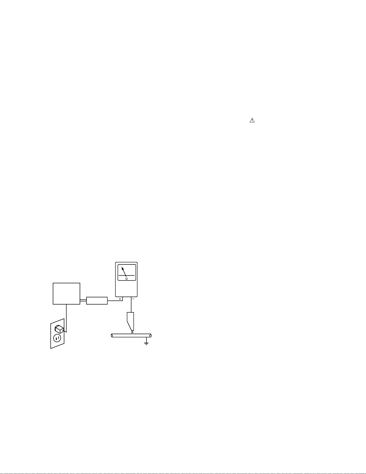
Leakage Current Cold Check
With the AC plug removed from an AC power source, place
a jumper across the two plug prongs. Turn the AC power
switch on. Using an insulation tester (DC 500V), connect
one lead to the jumpered AC plug and touch the other lead
to each exposed metal part (input/output terminals,
screwheads, metal overlays, control shafts, etc.),
particularly any exposed metal part having a return path
to the chassis. Exposed metal parts having a return path to
the chassis should have a minimum resistor reading of
0.3MΩ and a maximum resistor reading of 5MΩ. Any
resistor value below or above this range indicates an
abnormality which requires corrective action. Exposed
metal parts not having a return path to the chassis will
indicate an open circuit.
Leakage Current Hot Check
Plug the AC line cord directly into an AC power source
(do not use an isolation transformer for this check).
Turn the AC power switch on.
Using a "Leakage Current Tester (Simpson Model 229
equivalent)", measure for current from all exposed metal
parts of the cabinet (input/output terminals, screwheads,
metal overlays, control shaft, etc.), particularly any
exposed metal part having a return path to the chassis, to a
known earth ground (water pipe, conduit, etc.). Any
current measured must not exceed 0.5mA.
1.2 PRODUCT SAFETY NOTICE
Many electrical and mechanical parts in PIONEER set have
special safety related characteristics. These are often not
evident from visual inspection nor the protection afforded
by them necessarily can be obtained by using replacement
components rated for higher voltage, wattage, etc.
Replacement parts which have these special safety
characteristics are identified in this Service Manual.
Electrical components having such features are identified
by marking with a on the schematics and on the parts
list in this Service Manual.
The use of a substitute replacement component which dose
not have the same safety characteristics as the PIONEER
recommended replacement one, shown in the parts list in
this Service Manual, may create shock, fire or other
hazards.
Product Safety is continuously under review and new
instructions are issued from time to time. For the latest
information, always consult the current PIONEER Service
Manual. A subscription to, or additional copies of,
PIONEER Service Manual may be obtained at a nominal
charge from PIONEER.
Reading should
not be above
0.5mA
Earth
ground
Device
under
test
Also test with
plug reversed
(Using AC adapter
plug as required)
Test all
exposed metal
surfaces
Leakage
current
tester
AC Leakage Test
ANY MEASUREMENTS NOT WITHIN THE LIMITS
OUTLINED ABOVE ARE INDICATIVE OF A POTENTIAL
SHOCK HAZARD AND MUST BE CORRECTED BEFORE
RETURNING THE SET TO THE CUSTOMER.
3
Page 4
PDP-501MX, PDP-V501X
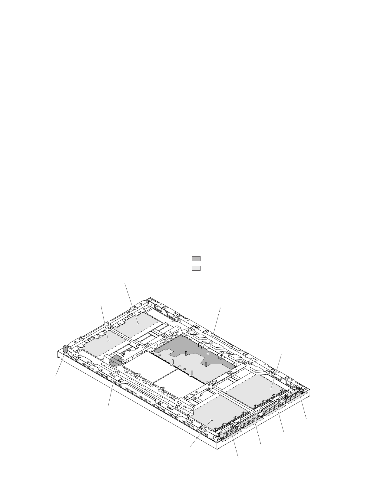
1.3 CHARGED SECTION AND HIGH VOLTAGE GENERATING POINT
7 Charged Section
The places where the commercial AC power is used
without passing through the power supply transformer.
If the places are touched, there is a risk of electric shock.
In addition, the measuring equipment can be damaged if it
is connected to the GND of the charged section and the
GND of the non-charged section while connecting the set
directly to the commercial AC power supply. Therefore,
be sure to connect the set via an insulated transformer and
supply the current.
7 Charged Section
(Power supply primary side)
1. AC Power Cord
2. AC Inlet with Filter
3. Power Switch (S1)
4. Fuse (In the MAIN POWER ASSY)
5. STB Transformer and Converter Transformer
(In the MAIN POWER ASSY)
6. Other primary side of the MAIN POWER ASSY
For the places, refer to the EXPLODED VIEWS, the
SCHEMATIC DIAGRAM and the PCB CONNECTION
DIAGRAM sections.
X DRIVE (A) ASSY
7 High Voltage Generating Point
The places where voltage is 100V or more except for the
charged places described above. If the places are touched,
there is a risk of electric shock.
1. POWER SUPPLY MODULE (170V)
2. X DRIVE (A) ASSY (170V)
3. X DRIVE (B) ASSY (170V)
4. Y DRIVE (A) ASSY (170V)
5. Y DRIVE (B) ASSY (170V)
6. SCAN ASSY (A),(B),(C),(D) (150V)
For the places, refer to the EXPLODED VIEWS, the
SCHEMATIC DIAGRAM and the PCB CONNECTION
DIAGRAM sections.
Part is charged section.
Part is the high voltage generating points other than
the charged section.
POWER SWITCH (S1)
4
X DRIVE (B) ASSY
AC INLET
POWER SUPPLY MODULE
Y DRIVE (B) ASSY
Y DRIVE (A) ASSY
SCAN A ASSY
SCAN B ASSY
SCAN C ASSY
SCAN D ASSY
Page 5
PDP-501MX, PDP-V501X
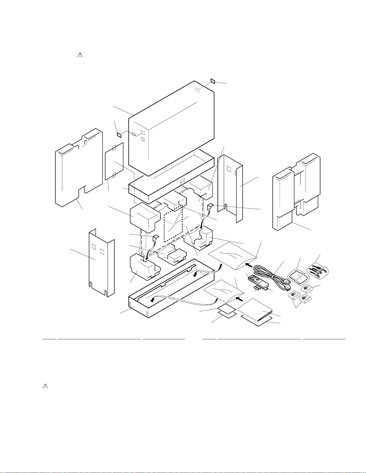
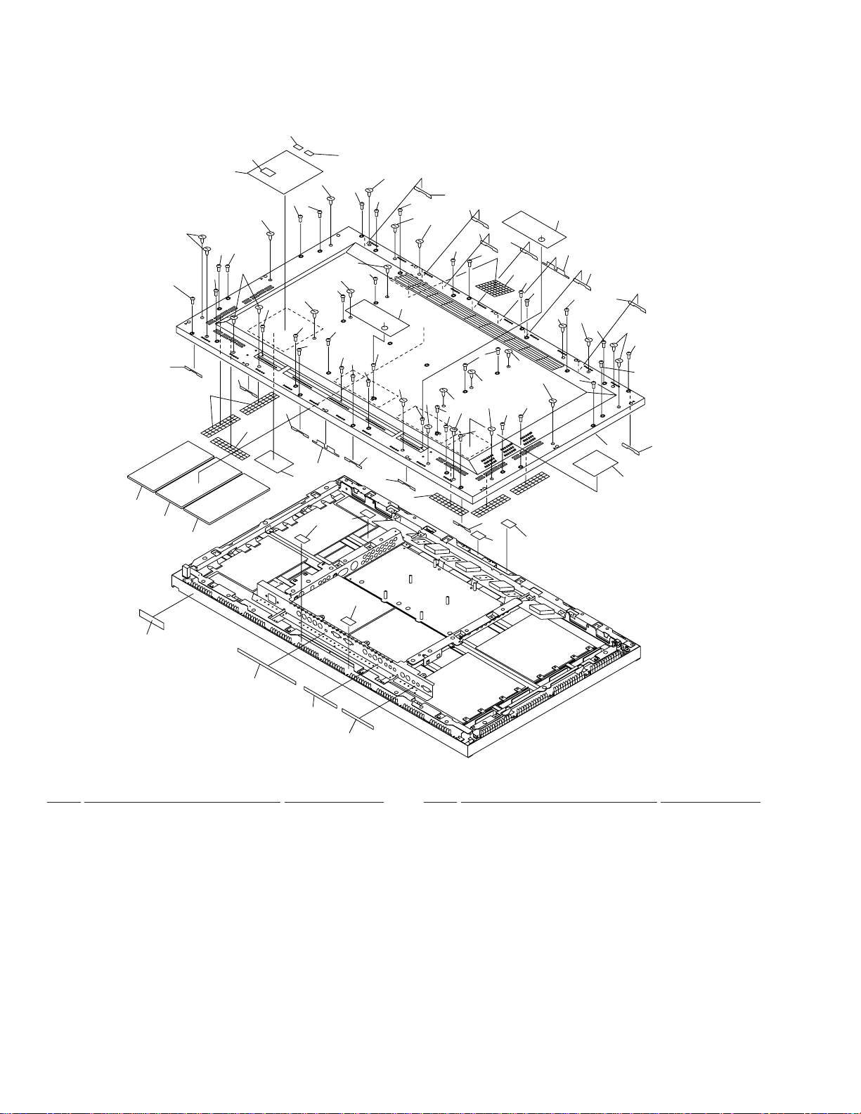
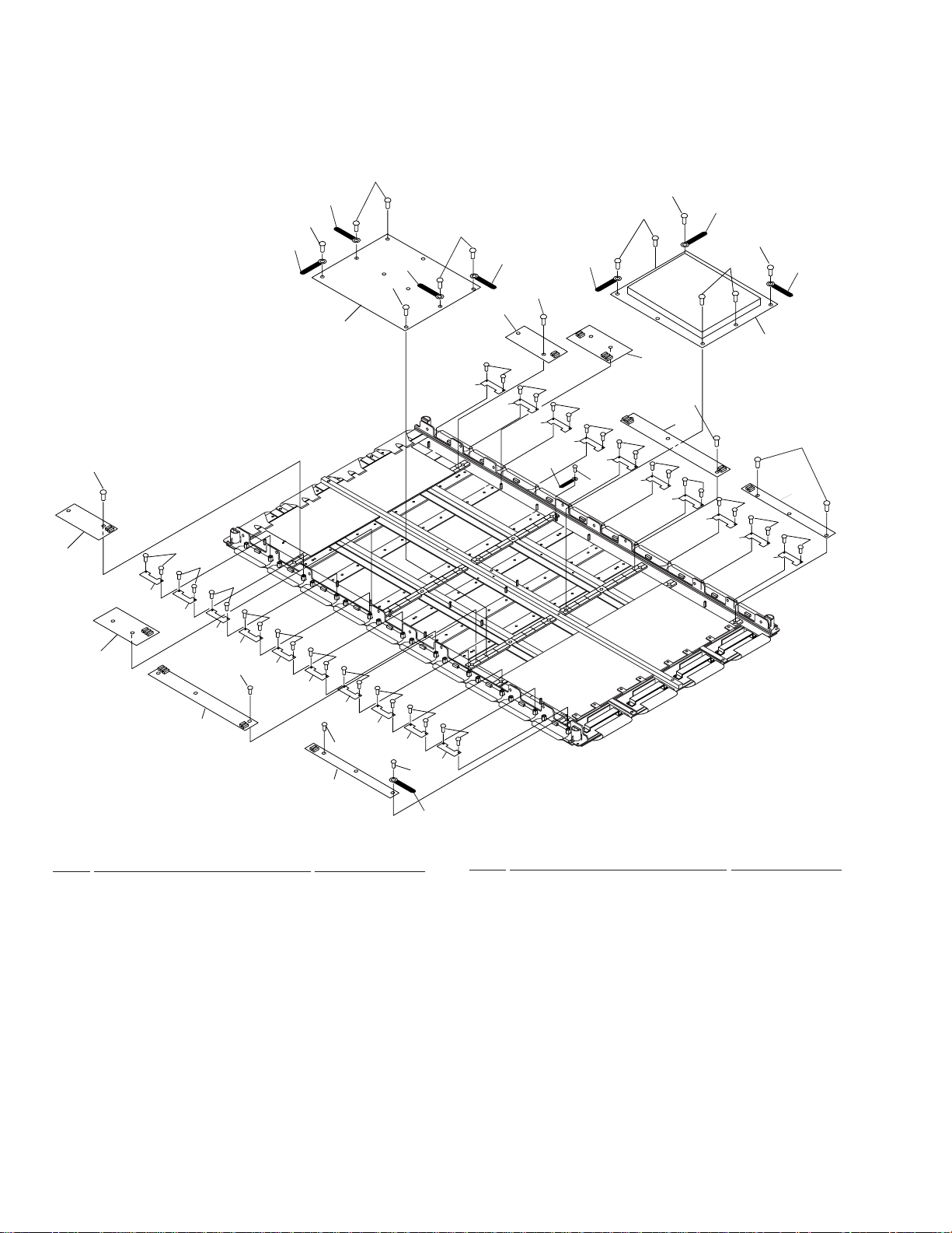
2. EXPLODED VIEWS AND PARTS LIST
NOTES:•Parts marked by "NSP" are generally unavailable because they are not in our Master Spare Parts List.
The mark found on some component parts indicates the importance of the safety factor of the part. Therefore, when
•
replacing, be sure to use parts of identical designation.
Screws adjacent to ¥ mark on the product are used for disassembly.
•
2.1 P ACKING
2
16
12
13
18
26
19
22
10
26
11
16
22
14
23
27
5
8
4
7
3
9
27
6
1
20
PARTS LIST
Mark No. Description Part No. Mark No. Description Part No.
NSP 1 Battery (R6P,AA) AEX-010
2 Rear Carton AHB1201
3 Binder Assy AEC1758
4 Wiping Cloth AED1174
5 Under Pad R AHA2213
6 Under Pad L AHA2214
7 AC Power Cord ADG1178
8 Mirror Mat AHG1284
9 Remote Control (SR) AXD1437
10 Under Pad C AHA2215
11 Upper Pad R AHA2216
12 Upper Pad L AHA2217
13 Upper Carton (501MX) AHD2980
13 Upper Carton (V501X) AHD2979
14 Upper Pad C AHA2218
15 Plasma Caution Sheet ARM1145
15
17
16 Side Carton AHB1196
17 Caution Sheet ARM1146
18 Protect Sheet SHC-925
19 Carton Cover AHD2975
20 UNDER CARTON ASSY AHD2976
21 Instruction Manual (501MX)
(English, French) ARE1337
21 Instruction Manual (V501X)
(English, French) ARE1339
22 Carton Spacer AHB1198
23 Front Carton AHB1200
24 BNC Conversion Connector
(501MX) AKX1052
NSP 25 Warranty Card (501MX) ARY1094
NSP 26 Label VRW1629
NSP 27 Literature Bag AHG-117
28 Battery Cover AZN2379
28
24
21
25
24
5
Page 6
PDP-501MX, PDP-V501X
2.2 REAR CASE
7
9
2
2
15
6
2
5
23
3
3
6
23
14
14
3
8
11
2
15
6
2
6
2
6
6
6
5
6
23
25
26
13
12
2
5
6
2
6
10
6
5
6
2
23
23
14
22
6
2
6
22
2
22
6
2
2
6
22
5
6
2
2
2
6
5
23
12
16
24
4
5
6
2
2
15
21
22
6
22
2
2
6
2
5
15
6
1
22
20
27
17
18
PARTS LIST
Mark No. Description Part No.
NSP 1 Rear Case (M) (501MX) AMR3097
NSP 1 Rear Case (MB) (V501X) AMR3100
2 Hole Rivet AMR2969
3 Barrier AMR3049
4 Net F AED1185
5 Screw BPZ40P160FZK
6 Screw AMZ30P100FZK
NSP 7 UPC Code Label (501MX) AAX2673
NSP 7 UPC Code Label (V501X) AAX2674
NSP 8 Label VRW1629
NSP 9 Name Label (501MX) AAL2274
NSP 9 Name Label (V501X) AAL2285
10 Terminal Label L (501MX) AAX2662
10 Terminal Label L (V501X) AAX2680
NSP 11 Manufactured Label AAX-372
12 IC Protector Label AAX2642
6
21
19
Mark No. Description Part No.
NSP 13 Drive Voltage Label ARW1077
14 Net R AED1178
15 Screw BMZ40P120FMC
16 Terminal Label R (501MX) AAX2663
16 Terminal Label R (V501X) AAX2679
17 Terminal Label 3 AAX2641
18 Terminal Label 2 AAX2640
19 Terminal Label 1 AAX2639
NSP 20 Bolt Caution Label (501MX) AAX2656
NSP 20 Bolt Caution Label (V501X) AAX2681
21 IC Protector Label (F) AAX2675
22 Rear Shield US ANK1574
23 Rear Shield DS ANK1575
24 Rear Shield UB ANK1576
25 Rear Shield DB ANK1577
26 Solder Warning Label AAX2644
27 Serial Sheet AAX1322
Page 7
PDP-501MX, PDP-V501X
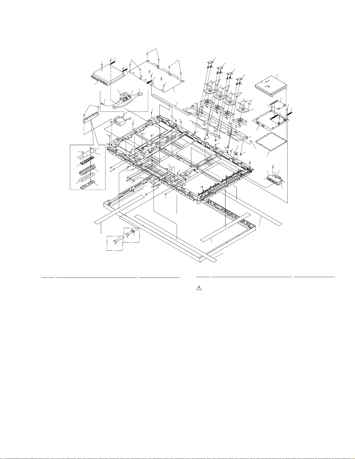
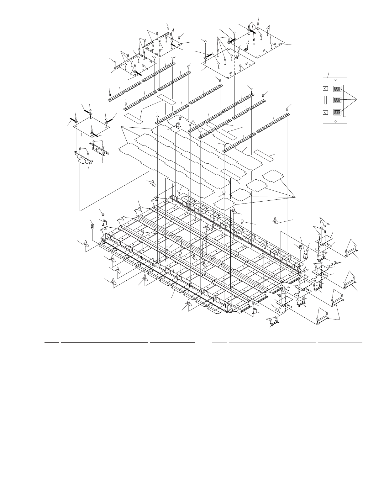
2.3 MAIN SECTION (1)
13
16
12
15
16
21
32
34
25
44
30
21
31
33
12
38
12
12
16
12
13
26
24
30
21
22
12
13
30
23
12
21
21
12
12
14
37
12
12
23
43
39
23
30
12
1
2
5
7
9
8
9
12
11
11
3
5
6
7
8
12
11
12
11
30
4
5
5
6
7
6
7
6
8
9
36
23
8
9
12
19
10
27
11
30
17
18
16
20
41
35
16
13
12
16
24
42
28
22
(for PDP-V501X)
40
12
(for PDP-501MX)
PARTS LIST
Mark No. Description Part No.
1 DC FAN A ASSY AWZ6323
2 DC FAN B ASSY AWZ6324
3 DC FAN C ASSY AWZ6325
4 DC FAN D ASSY AWZ6326
5 Locking Card Spacer AEC1736
6 Fan Cushion B AEC1750
7 Fan Cushion A AEC1749
8 Fan Filter DNH1548
9 Fan Motor 80*25 AXM1032
NSP 10 Fan Angle ANG2237
11 Screw PPZ50P100FZK
12 Screw BMZ30P060FCU
13 Binder AEP-215
14 Power Supply Module AXY1029
15 RGB ASSY AWV1687
16 Screw AMZ30P080FCU
NSP 17 Analog Shield A ANK1536
NSP 20 Analog Shield B ANK1537
18 PROGRESSIVE BLOCK AWZ6222
19 VIDEO ASSY AWZ6305
21 Screw BPZ30P080FZK
22 Screw BBA1017
23 Screw BPZ40P160FZK
29
28
29
Mark No. Description Part No.
24 Ferrite Core ATX1031
25 AC Inlet with Filter AKP1180
26 Housing Wire ADX2406
27 SENSOR A ASSY AWZ6309
28 Panel Sheet B AMR2958
NSP 29 Panel Sheet H AMR3035
30 Screw BMZ40P120FMC
31 SIDE SWITCH ASSY AWZ6315
32 Control Button AAC1536
NSP 33 Control PCB Holder ANG2292
34 Blind Cover AMR3098
35 CONTROL ASSY AWZ6307
36 SENSOR B ASSY AWZ6310
37 Shield Gusket A ANK1578
38 Control Name Plate (501MX) AAK2719
38 Control Name Plate (V501X) AAK2720
39 Terminal Cover (501MX) AMR3099
40 Terminal Cover (232C) (501MX)ANG2294
NSP 41 232C Case A ANK1567
NSP 42 232C Case B ANK1568
43 Fan Barrier AMR3124
44 Ground Wire (J13) ADX2332
7
Page 8
PDP-501MX, PDP-V501X
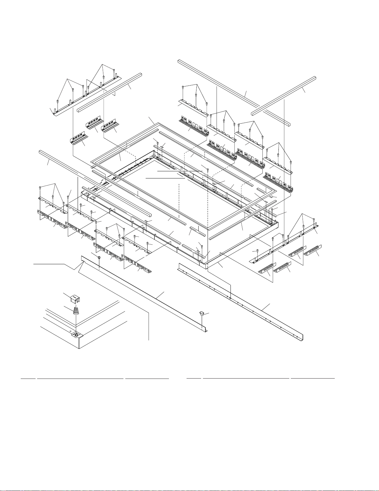
2.4 FRONT CASE SECTION
11
11
17
6
4
7
7
16
10
10
5
8
10
11
5
8
13
15
11
7
20
10
5
8
5
10
15
10
10
8
5
15
18
21
19
8
18
15
10
10
10
5
22
16
10
10
8
5
8
15
23
15
20
11
3
10
5
8
19
10
11
7
24
17
11
6
7
7
7
12
9
PARTS LIST
Mark No. Description Part No.
1 Sash U AAP1583
2 Sash D (N) AAP1591
3 Front Case (M) (501MX) AMB2632
3 Front Case (M) (V501X) AMB2624
4 PROTECT PANEL ASSY AMR3065
NSP 5 Panel Holder H ANG2228
6 Panel Holder V ANG2277
7 Panel Shield FV ANK1541
8 Panel Shield FH ANK1542
9 Coil Spring ABH1103
10 Screw PMZ40P080FMC
11 Screw BPZ40P080FZK
12 Power Button AAD4101
8
2
1
14
Mark No. Description Part No.
13 LED Lens AAK2695
14 Lens AAK2703
NSP 15 Sheet AED1176
16 Panel Cushion 50H AED1181
17 Panel Cushion 50V AED1182
18 Shield Gusket F ANK1583
19 Shield Gusket E ANK1582
20 Shield Gusket D ANK1581
21 Shield Gusket G ANK1584
22 Shield Gusket H ANK1585
23 Shield Gusket C ANK1580
24 Shield Gusket B ANK1579
Page 9
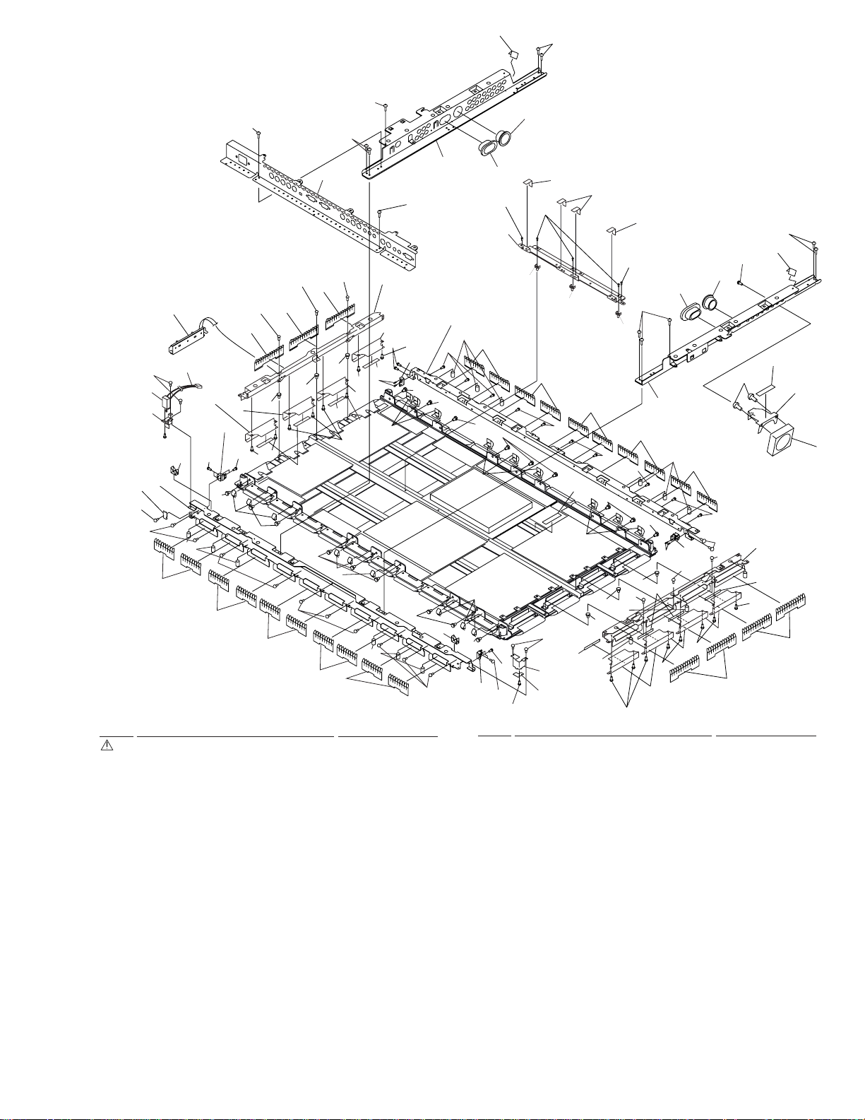
2.5 MAIN SECTION (1)
14
14
14
26
30
PDP-501MX, PDP-V501X
14
10
13
13
6
13
39
6
6
19
14
2
1
34
24
11
22
11
11
33
25
24
15
25
25
15
28
9
25
33
4
17
8
13
23
13
11
27
11
11
27
7
7
13
7
7
23
7
PARTS LIST
Mark No. Description Part No.
1 Power Switch ASG1082
2 Housing Wire (J12) ADX2407
3 Frame V ANG2232
4 Frame HD ANG2233
5 Frame HU ANG2234
33
27
3
24
28
22
11
14
25
11
13
32
31
18
14
21
12
26
21
26
14
14
26
31
30
25
14
26
5
13
23
7
21
37
7
38
36
11
27
11
11
13
37
7
13
11
27
13
7
11
29
15
23
22
35
7
13
28
3
13
13
11
23
13
25
24
33
25
24
24
25
27
9
14
11
22
15
28
20
16
33
11
11
23
8
Mark No. Description Part No.
NSP 21 PCB Mold AMR2115
22 Corner Holder AMR3067
23 VCP Cap AEC1760
24 FPC Shield ANK1550
25 Screw BBZ30P060FMC
33
25
6
6
6 Panel Shield RV ANK1539
7 Panel Shield RH ANK1540
8 Nyron Rivet AEC1671
9 Edging Saddle AEC1737
10 Terminal Panel ANG2310
11 Well Nut ABN1029
12 Screw AMZ30P140FCU
13 Screw BMB30P140FZK
14 Screw BMZ30P060FCU
15 Screw
16 IR RECEIVER ASSY AWZ6224
17 INDICAT OR ASSY AWZ6225
NSP 18 Center Frame ANG2230
NSP 19 Switch Holder ANG2239
NSP 20 Holder ANG2240
26 Frame Sheet AED1173
27 Shield Finger ABX1004
28 Screw AMZ30P100FZK
29 Sub Frame R ANG2303
NSP 30 Bush A AEC1738
NSP 31 Bush C AEC1740
32 Sub Frame L ANG2236
33 FPC Cushion AEB1341
34 FPC Shield (M) ANK1561
35 Fan Motor AXM1026
36 Fan Angle B ANG2301
37 Fan Cushion B AEC1750
38 Screw PPZ50P100FZK
39 Side Switch Assy AWZ6315
9
Page 10
PDP-501MX, PDP-V501X
2.6 MAIN SECTION (3)
13
25
2
4
25
1
2
4
2
4
2
25
4
2
4
25
2
12
14
5
6
3
23
21
4
3
3
19
3
3
15
4
3
16
17
1
4
9
3
3
3
18
3
20
22
4
8
3
3
24
3
24
22
20
7
11
18
4
16
3
3
3
17
4
19
3
3
3
21
4
3
23
15
10
2
PARTS LIST
Mark No. Description Part No.
1 Binder AEC-826
2 Binder AEP-215
3 Screw BMZ30P040FMC
4 Screw BPZ30P080FZK
5 DIGITAL VIDEO ASSY AWV1728
6 CABLE E ASSY AWZ6218
7 CABLE F ASSY AWZ6219
8 CABLE A ASSY AWZ6214
9 CABLE B ASSY AWZ6215
10 CABLE C ASSY AWZ6216
11 CABLE D ASSY AWZ6217
12 CABLE G ASSY AWZ6220
13 CABLE H ASSY AWZ6221
10
Mark No. Description Part No.
14 U-CON ASSY AWV1689
15 PUMP UP A ASSY AWZ6249
16 PUMP UP B ASSY AWZ6250
17 PUMP UP C ASSY AWZ6251
18 PUMP UP D ASSY AWZ6252
19 PUMP UP E ASSY AWZ6253
20 PUMP UP F ASSY AWZ6254
21 PUMP UP G ASSY AWZ6255
22 PUMP UP H ASSY AWZ6256
23 PUMP UP K ASSY AWZ6257
24 PUMP UP L ASSY AWZ6258
25 Screw AMZ30P140FCU
Page 11
2.7 MAIN SECTION (4)
21
21
21
12
12
16
7
8
11
7
11
11
7
34
21
11
11
7
21
1
1
11
7
2
28
31
12
PDP-501MX, PDP-V501X
12
11
21
25
21
8
21
11
12
12
15
7
7
11
8
14
8
8
5
11
32
21
21
21
8
10
8
11
11
10
10
77
10
7
10
10
10
11
8
8
29
8
8
2
30
11
10
13
17, 18, 19, 20
11
8
30
6
23
5
9
25
31
31
31
31
31
27
PARTS LIST
Mark No. Description Part No.
NSP 1 3D Y/C Holder ANG2293
NSP 5 Rivet AEC1748
2 Panel Shield L ANK1548
3 Panel Shield S ANK1553
4 Hot Plate ANG2231
6 Sheet AEH1027
7 Binder AEP-215
8 PCB Spacer AMR3037
9 Spacer AEF1026
10 Screw AMZ30P140FCU
11 Screw BMZ30P060FCU
12 Screw BPZ30P080FZK
13 Y DRIVE A ASSY AWV1695
14 Y DRIVE B ASSY AWV1696
15 X DRIVE A ASSY AWZ6242
16 X DRIVE B ASSY AWZ6243
17 SCAN A ASSY AWZ6226
31
32
19
3
31
25
9
26
6
31
32
33
31
32
11
20
26
5
25
22
4
Mark No. Description Part No.
18 SCAN B ASSY AWZ6227
19 SCAN C ASSY AWZ6228
20 SCAN D ASSY AWZ6229
21 Screw AMZ30P080FCU
22 Screw IPZ30P080FCU
NSP 23 FRAME ASSY(AL) ANA1544
NSP 24 Scan Heatsink ANH1544
NSP 25 Tube Cover AMR3036
NSP 26 PVC Sheet AMR3038
NSP 27 PLASMA PANEL ASSY AAV1229
NSP 28 Frame Barrier X AMR3062
NSP 29 Frame Barrier C AMR3063
NSP 30 Frame Barrier Y AMR3064
NSP 31 Circuit Board Spacer AEC1744
NSP 32 PCB Spacer AEC1573
NSP 33 Circuit Board Spacer AEC1743
34 3D Y/C SEP. ASSY AWZ6332
6
11
5
11
6
11
22
4
21
17
21
26
22
4
6
24
21
24
24
18
26
22
21
4
11
Page 12
1
2
S
23
PDP-501MX, PDP-V501X
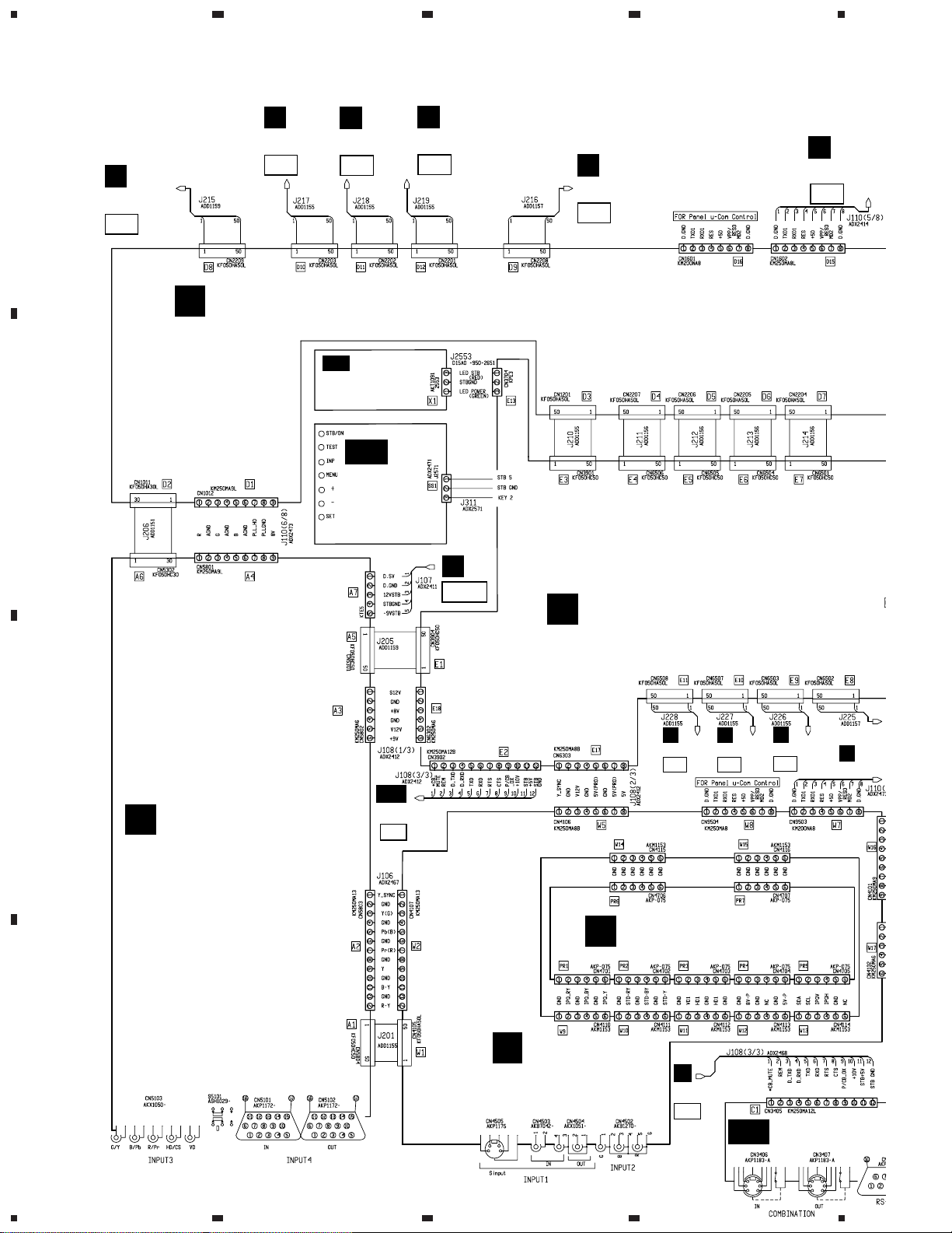
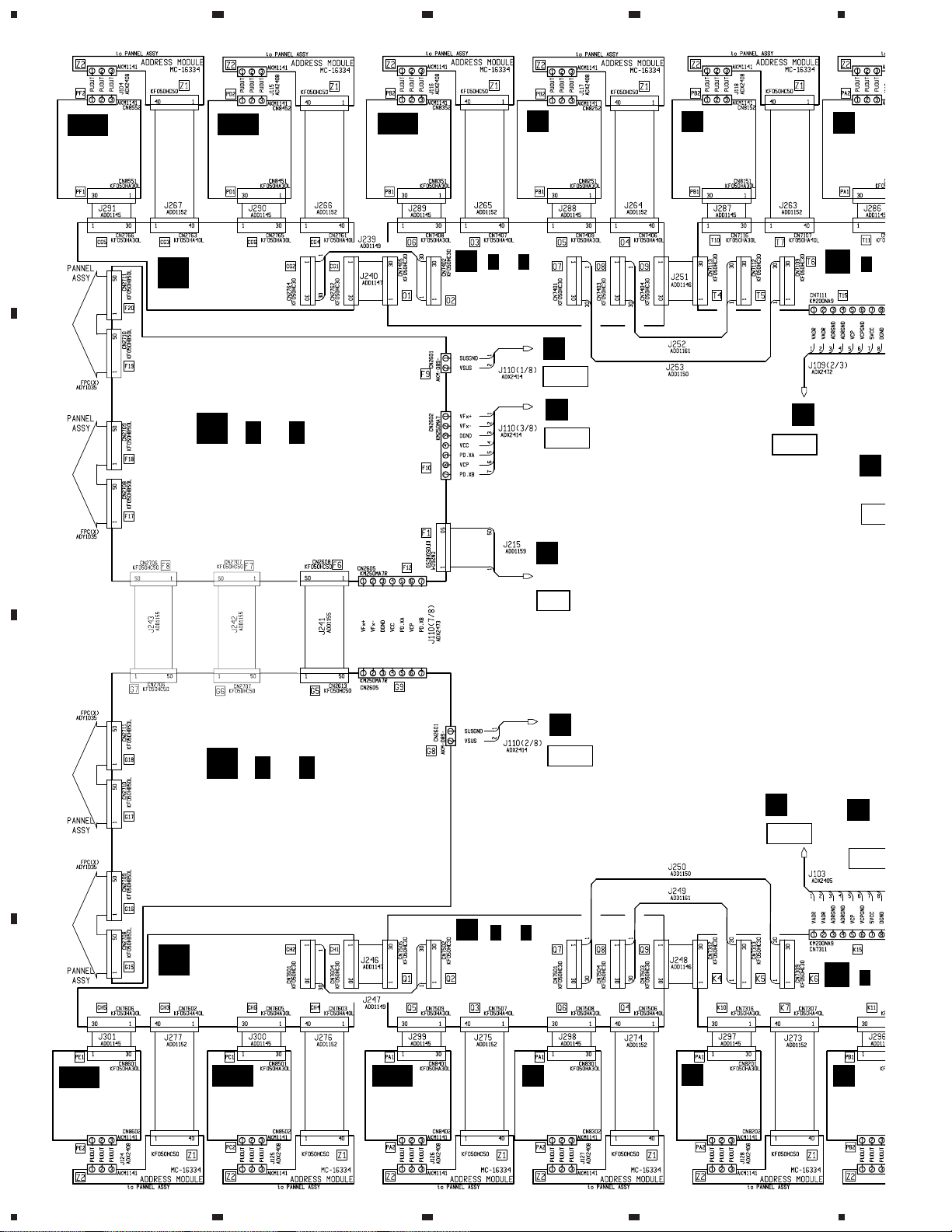
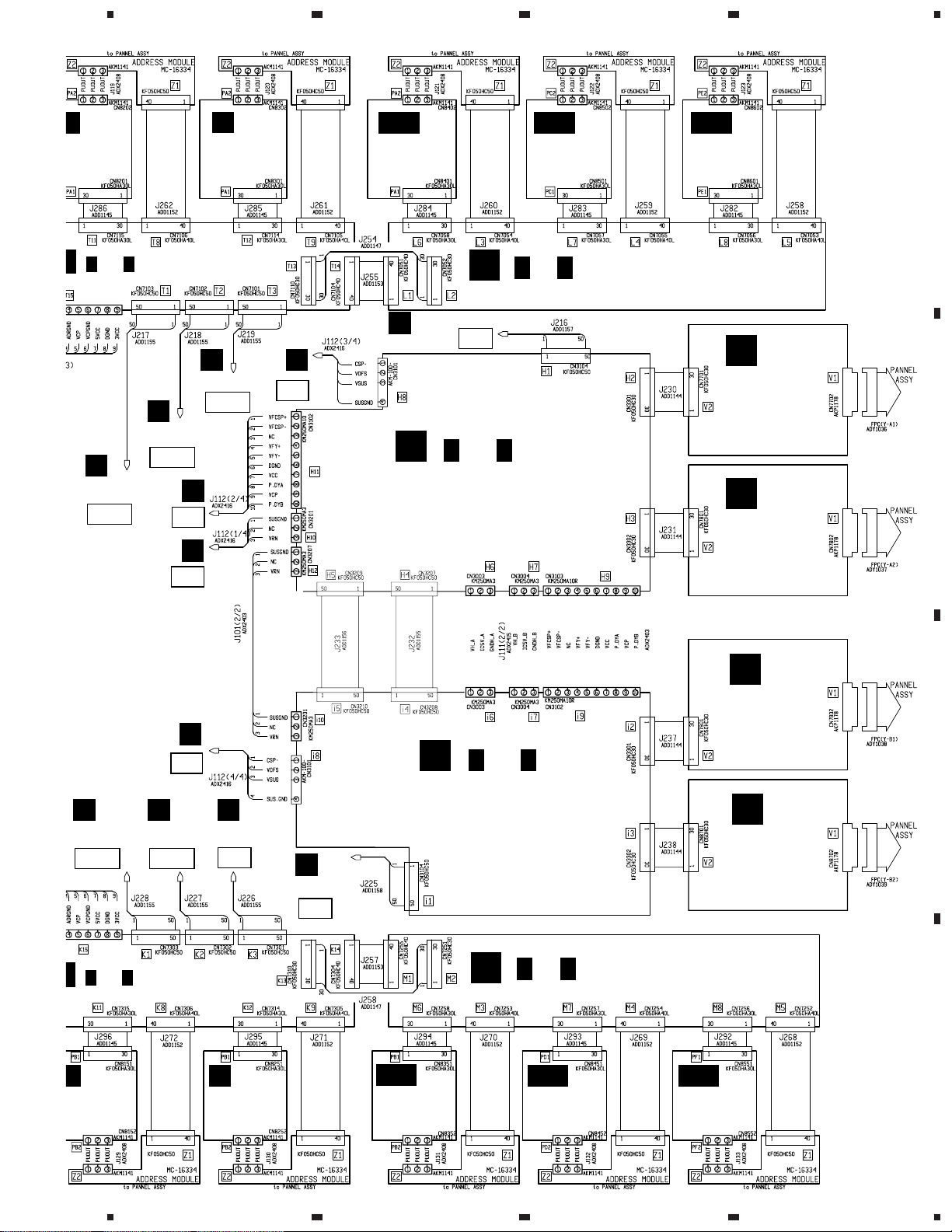
3. SCHEMATIC DIAGRAM
3.1 OVERALL CONNECTION DIAGRAM (1/2)
L
CN7103
A
T1
E
CN2604
F1
D
DIGITAL VIDEO ASSY (AWV1728)
L
CN7102
T2
AH
INDICATOR
ASSY
(AWZ6225)
L
CN7101
T3
G
CN3104
H1
4
A
CN4101
B7
B
AQ
SIDE
SWITCH
ASSY
(AWZ6315)
J5101
J
P20
I
U-CON ASSY (AWV1689)
N
CN7303
C
K1
N
CN7302
K2
AO
C
CN3405
C1
RGB ASSY (AWV1687)
N
CN7301
K3
D
CN160
PROGESSIVE BLOCK
B
(AWZ6222)
A
D
VIDEO ASSY
(AWZ6305)
12
1234
I
CN3902
E2
AO
CONTROL A
(AWZ6307)
Page 13
5
Note: When ordering service parts, be sure to refer to “EXPLODED VIEWS and
PARTS LIST” or “PCB PARTS LIST”
678
PDP-501MX, PDP-V501X
A
CN4101
B7
E
CN2601
F9
E
CN2602
F10
F
CN2601
G8
J
(
1/2 ,
J
L
CN7111
T15
2/2
J
)
POWER SUPPLY MODULE
(AXY1029)
N
CN7311
K15
G
CN3101
H8
G
CN3102
H11
G
CN3201
H10
H
CN3101
I 8
A
B
H
CN3104
301
D
CN1602
I 1
K
NTROL ASSY
Z6307)
D15
AG
J311
ADX2475
IR RECEIVE
ASSY
(AWZ6224)
A I
DC FAN A ASSY
(AWZ6323)
AM
AP
SENSOR A
ASSY
3D Y/C SEP. ASSY
(AWZ6332)
(AWZ6309)
AP
AK
DC FAN C ASSY
(AWZ6325)
AKC1002
K8601
DC FAN B
ASSY
(AWZ6324)
AJ
C
J5101
A7
Y312
YJSHA0-20-5/5
K8602
AKC1002
AN
SENSOR B
ASSY
(AWZ6310)
C
AL
DC FAN D
ASSY
(AWZ6326)
D
5
6
7
13
8
Page 14
1
P
0
P
4
1
PDP-501MX, PDP-V501X
23
4
3.2 OVERALL CONNECTION DIAGRAM (2/2)
O
1/2,
Y
PUMP UP C
ASSY
(AWZ6251)
O
2/2
)
AE
PUMP UP K
A
ASSY
(AWZ6257)
Q
AC
PUMP UP G
ASSY
(AWZ6255)
CABLE G
ASSY
(AWZ6220)
AA
PUMP UP E
ASSY
(AWZ6253)
(
O
CABLE E
ASSY
(AWZ6218)
W
PUMP UP A
ASSY
(AWZ6249)
X
PUMP U
ASSY
(AWZ625
L
(
L
1/3
J
P11
J
E
E
(
B
X DRIVE A ASSY
(AWZ6242)
1/2,
E
2/2
)
P12
J
P17
D
CN
D
D
CN2209
D8
J
C
F
F
(
)
2/2
F
1/2,
X DRIVE B ASSY
(AWZ6243)
P
1/2,
P
(
CABLE H
R
ASSY
(AWZ6221)
D
AF
PUMP UP L
ASSY
(AWZ6258)
AD
PUMP UP H
ASSY
(AWZ6256)
AB
PUMP UP F
ASSY
(AWZ6254)
CABLE F
ASSY
(AWZ6219)
P14
2/2
P
)
Z
PUMP UP D
ASSY
(AWZ6252)
X
PUMP UP B
ASSY
(AWZ6250)
J
P18
I
CN6
E11
(
N
W
PUMP U
ASSY
(AWZ62
1/3
N
14
1234
Page 15
5
678
PDP-501MX, PDP-V501X
MP UP B
SSY
WZ6250)
1/3 –
L
(
D
CN2203
D10
CABLE B ASSY
3/3
L
)
(AWZ6215)
D
CN2201
D
CN2202
D11
J
P6
J
P7
Z
PUMP UP D
ASSY
(AWZ6252)
D12
J
P5
AB
PUMP UP F
ASSY
(AWZ6254)
D
CN2208
1
2
3
4
G
(
Y DRIVE A ASSY
(AWZ6321)
1/4 –
G
K
D9
G
(
K
4/4
AD
PUMP UP H
ASSY
(AWZ6256)
2/2
K
1/2,
)
AF
PUMP UP L
ASSY
(AWZ6258)
)
CABLE A ASSY
(AWZ6214)
S
SCAN A
ASSY
(AWZ6226)
T
SCAN B
ASSY
(AWZ6227)
A
B
I
CN6508
E11
1/3 –
N
(
UMP UP A
SSY
WZ6249)
J
P8
I
CN6507
E10
CABLE D ASSY
3/3
N
)
(AWZ6217)
I
CN6503
E9
Y
PUMP UP C
ASSY
(AWZ6251)
I
CN6502
E8
H
(
1/4 –
H
Y DRIVE B ASSY
(AWZ6322)
M
AA
PUMP UP E
ASSY
(AWZ6253)
4/4
H
1/2,
M
(
AC
PUMP UP G
ASSY
(AWZ6255)
)
M
CABLE C ASSY
2/2
)
(AWZ6216)
AE
PUMP UP K
ASSY
(AWZ6257)
U
SCAN C
ASSY
(AWZ6228)
C
V
SCAN D
ASSY
(AWZ6229)
D
5
6
7
15
8
Page 16
1
23
PDP-501MX, PDP-V501X
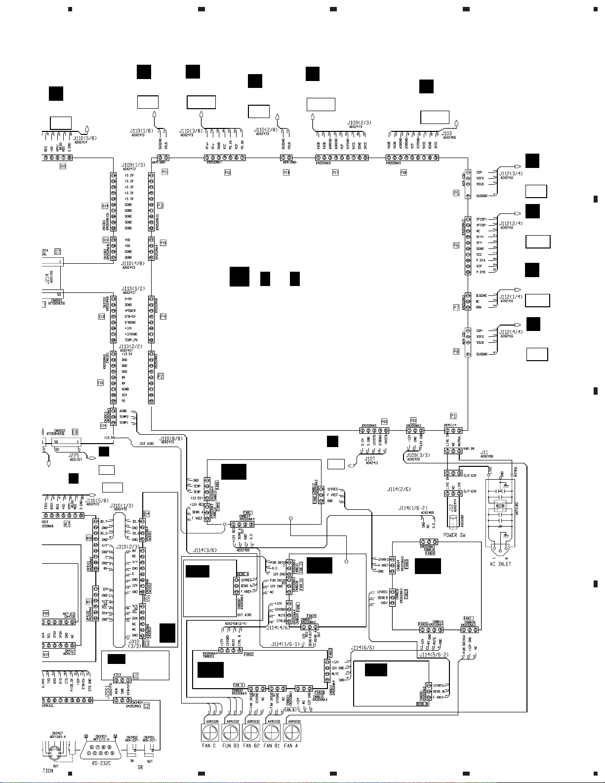
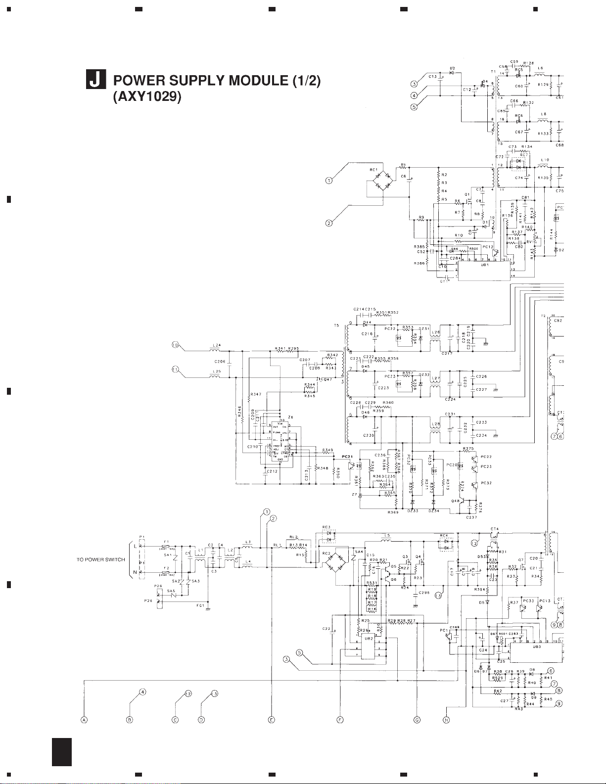
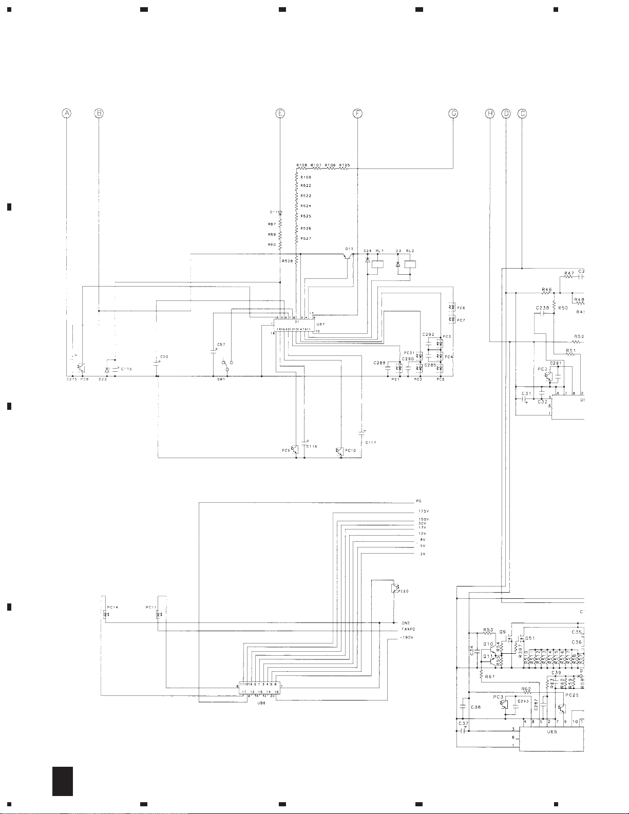
3.3 POWER SUPPLY MODULE (1/2)
A
B
4
C
D
J
16
1/2
1234
Page 17
5
678
PDP-501MX, PDP-V501X
A
B
5
6
J
7
C
D
17
1/2
8
Page 18
1
23
PDP-501MX, PDP-V501X
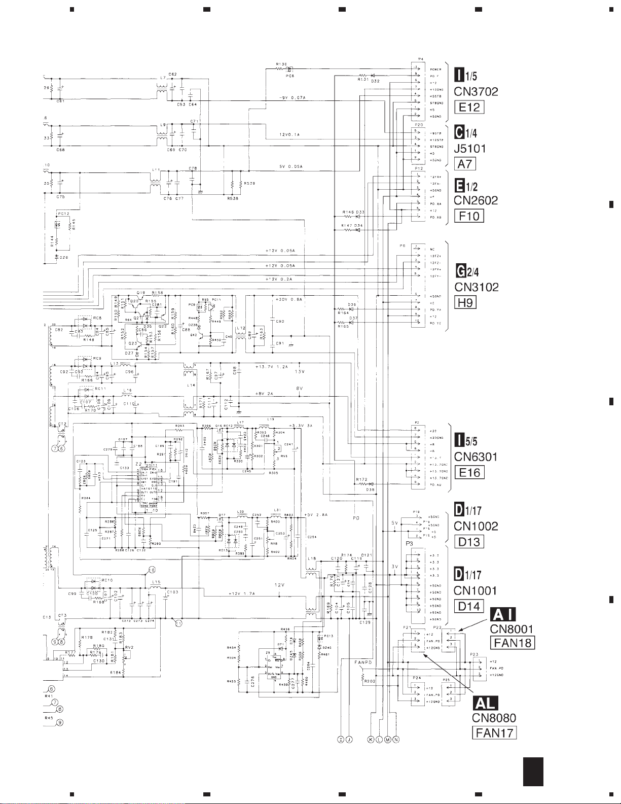
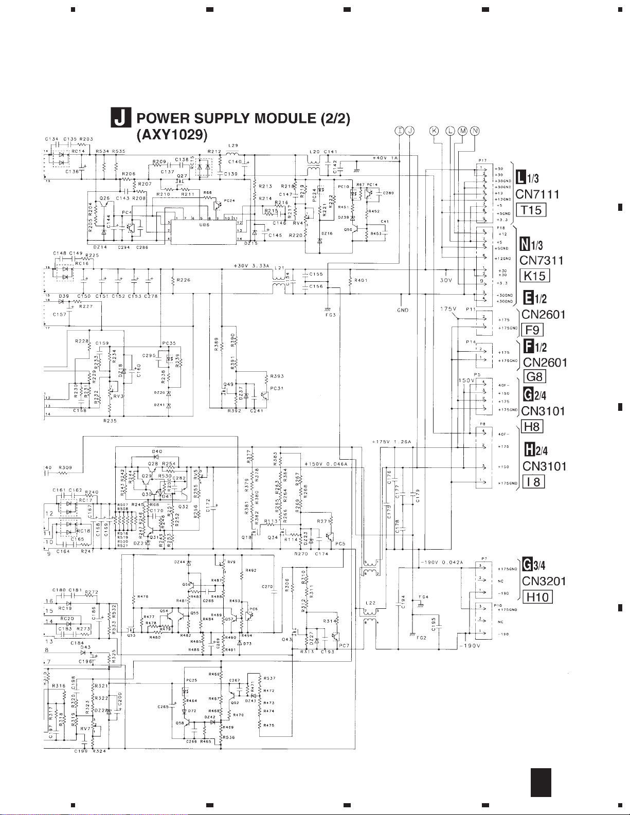
3.4 POWER SUPPLY MODULE (2/2)
A
B
4
C
D
18
J
2/2
1234
Page 19
5
678
PDP-501MX, PDP-V501X
A
B
5
6
J
7
C
D
19
2/2
8
Page 20
PDP-501MX ,PDP-V501X
4. PCB CONNECTION DIAGRAM
Mark No. Description Part No.
There is no information to be shown in this chapter.
5. PCB PARTS LIST
NOTES:
Mark No. Description Part No.
LIST OF ASSEMBLIES
NSP CONNECTOR ASS'Y AWV1647
NSP SCAN ASS'Y AWV1653
NSP PUMP UP ASSY AWV1656
NSP ANALOG VIDEO ASS'Y AWV1685
Parts marked by "NSP" are generally unavailable because they are not in our Master Spare Parts List.
The mark found on some component parts indicates the importance of the safety factor of the part.
Therefore, when replacing, be sure to use parts of identical designation.
When ordering resistors, first convert resistance values into code form as shown in the following examples.
Ex.1 When there are 2 effective digits (any digit apart from 0), such as 560 ohm and 47k ohm (tolerance is shown by J=5%,
and K=10%).
560
47k
0.5
1
56 x 10
47 x 103
R50
1R0
1
561
473
Ex.2 When there are 3 effective digits (such as in high precision metal film resistors).
5.62k RN1/4PC F562 x 10
DIGITAL VIDEO ASS'Y AWV1728
CABLE A ASS'Y AWZ6214
CABLE B ASS'Y AWZ6215
CABLE C ASS'Y AWZ6216
CABLE D ASS'Y AWZ6217
CABLE G ASS'Y AWZ6220
CABLE H ASS'Y AWZ6221
PROGRESSIVE BLOCK AWZ6222
IR RECEIVER ASS'Y AWZ6224
INDICAT OR ASS'Y AWZ6225
SCAN A ASS'Y AWZ6226
SCAN B ASS'Y AWZ6227
SCAN C ASS'Y AWZ6228
SCAN D ASS'Y AWZ6229
PUMP UP A ASSY AWZ6249
PUMP UP B ASSY AWZ6250
PUMP UP C ASSY AWZ6251
PUMP UP D ASSY AWZ6252
PUMP UP E ASSY AWZ6253
PUMP UP F ASSY AWZ6254
PUMP UP G ASSY AWZ6255
PUMP UP H ASSY AWZ6256
PUMP UP K ASSY AWZ6257
PUMP UP L ASSY AWZ6258
VIDEO ASS'Y AWZ6305
CONTROL ASS'Y AWZ6307
RGB ASS'Y AWV1687
U-CON ASS'Y AWV1689
1
5621
Mark No. Description Part No.
RD1/4PU J
RD1/4PU J
RN2H K
RS1P K
561
473
R50
1R0
5621
Mark No. Description Part No.
NSP X DRIVE A ASS'Y AWV1692
NSP X DRIVE B ASS'Y AWV1698
D
CABLE E ASS'Y AWZ6218
X DRIVE A ASS'Y AWZ6242
SENSER A ASSY AWZ6309
SENSER B ASSY AWZ6310
Y DRIVE A ASS'Y AWV1695
Y DRIVE A ASS'Y AWZ6321
DC FAN A ASSY AWZ6323
DC FAN B ASSY AWZ6324
Y DRIVE B ASS'Y AWV1696
Y DRIVE B ASS'Y AWZ6322
DC FAN C ASSY AWZ6325
DC FAN D ASSY AWZ6326
CABLE F ASS'Y AWZ6219
X DRIVE B ASS'Y AWZ6243
3D Y/C SEP. ASS'Y A WV1709
SIDE SWITCH A AWZ6315
3D Y/C SEP . ASS'Y AWZ6332
POWER SUPPLY MODULE AXY1029
DIGITAL VIDEO ASS'Y
SEMICONDUCTORS
IC1131,IC1151,IC1171 CXA3026Q
IC1242 CXA3106Q
IC1601 HD64F3048F16
IC1056 KIA431F
IC1301 PD4891B
IC1351 PD4892A
IC1401,IC1451,IC1501 PD4893B
IC1551 PD4894A
IC1271 PD5447A
IC1286 PDY038B
20
IC1603 PST9146N
IC1001-IC1004 TA78M05F
IC1901,IC1902,IC1951,IC1955-IC1957 TC74LCX541FT
IC1201,IC1221,IC1903-IC1906 TC74VHC541FT
IC1952-IC1954,IC2001-IC2010 TC74VHC541FT
Page 21

PDP-501MX, PDP-V501X
Mark No. Description Part No.
IC2101-IC2110 TC74VHC541FT
IC1046 TC74VHCT541AFT
IC1273 TC7SET00FU
IC1272 TC7SET08FU
IC1243,IC1244 TC7SH04FU
IC1651,IC1652 TC7W08FU
IC1604 TC7W14FU
IC1241 UPC78L05T
IC1701,IC1702,IC1751,IC1752 UPD481850GF-A12
IC1801,IC1802 UPD481850GF-A12
Q1072 ,Q1073 ,Q1082 ,Q1083 2SA1037K
Q1092 ,Q1093 2SA1037K
Q1071 ,Q1074 ,Q1081 ,Q1084 ,Q1091 2SC2412K
Q1094 ,Q1102 ,Q1103 ,Q1112 ,Q1113 2SC2412K
Q1122 ,Q1123 2SC2412K
D1601 -D1603 1SS352
D1901 AEL1171
COIL AND FILTERS
F1017 -F1020 ATF1184
F1551 -F1556 ,F1561 ,F1562 ATF1188
F1901 -F1908 ,F1951 -F1954 ATF1188
F2001 -F2010 ,F2101 -F2110 ATF1188
F1001 -F1014 ,F1241 ,F1242 ,F1921 ATF1189
F1971 ,F1972 ATF1189
SWITCH AND RELAY
S1601 ASG9003
CAP ACITORS
C1262 ,C1268 (0.33µF/16V) ACE1116
C1301 -C1310 ,C1351 -C1362
(1µF/16V) ACG1051
C1401 -C1412 ,C1451 -C1462
(1µF/16V) ACG1051
C1501 -C1512 ,C1551 -C1555
(1µF/16V) ACG1051
C1261 ,C1617 -C1621 CCSQCH101J50
C1203 -C1210 ,C1256 -C1258 ,C1264 CCSQCH220J50
C1276 -C1278 ,C1285 ,C1298 ,C1299 CCSQCH220J50
C1078 ,C1114 ,C1124 CCSQCH330J50
C1274 CCSQCH470J50
C1263 CCSQSL122J50
C1003 ,C1009 ,C1015 ,C1021 ,C1033 CEV101M6R3
C1037 ,C1056 ,C1057 ,C1133 ,C1145 CEV101M6R3
C1153 ,C1160 ,C1173 ,C1180 ,C1201 CEV101M6R3
C1243 ,C1245 ,C1254 ,C1271 ,C1289 CEV101M6R3
C1293 ,C1311 ,C1312 ,C1371 ,C1372 CEV101M6R3
C1421 ,C1422 ,C1471 ,C1472 CEV101M6R3
C1521 ,C1522 ,C1561 ,C1562 CEV101M6R3
C1631 ,C1632 ,C1721 -C1724 CEV101M6R3
C1771 -C1774 ,C1821 -C1824 CEV101M6R3
C1922 ,C1923 ,C1972 ,C1973 ,C1975 CEV101M6R3
C2021 ,C2022 ,C2121 ,C2122 CEV101M6R3
C1074 ,C1076 ,C1084 ,C1086 ,C1094 CEV1R0M50
C1096 ,C1275 ,C1606 CEV1R0M50
C1001 ,C1007 ,C1013 ,C1019 ,C1031 CEV221M10
C1035 ,C1240 CEV221M10
Mark No. Description Part No.
C1241 CEV470M16
C1602 CEV4R7M35
C1273 CFHSQ103J16
C1616 CKSQYB102K50
C1073 ,C1075 ,C1083 ,C1085 ,C1093 CKSQYB103K50
C1095 ,C1259 ,C1281 ,C1559 ,C1603 CKSQYB103K50
C1607 ,C1609 ,C1651 ,C1652 CKSQYB103K50
C1002 ,C1004 ,C1008 ,C1010 ,C1014 CKSQYF104Z25
C1016 ,C1020 ,C1022 ,C1032 ,C1034 CKSQYF104Z25
C1036 ,C1038 ,C1047 ,C1058 CKSQYF104Z25
C1063 ,C1064 ,C1071 ,C1072 CKSQYF104Z25
C1081 ,C1082 ,C1091 ,C1092 CKSQYF104Z25
C1102 ,C1103 ,C1112 ,C1113 CKSQYF104Z25
C1122 ,C1123 ,C1131 ,C1132 CKSQYF104Z25
C1134 -C1139 ,C1141 ,C1143 ,C1144 CKSQYF104Z25
C1146 ,C1151 ,C1152 ,C1154 -C1159 CKSQYF104Z25
C1161 ,C1163 ,C1164 ,C1166 CKSQYF104Z25
C1171 ,C1172 ,C1174 -C1179 ,C1181 CKSQYF104Z25
C1183 ,C1184 ,C1186 ,C1202 ,C1222 CKSQYF104Z25
C1242 ,C1244 ,C1246 -C1253 ,C1255 CKSQYF104Z25
C1260 ,C1266 ,C1267 ,C1272 ,C1279 CKSQYF104Z25
C1282 -C1284 ,C1287 ,C1288 CKSQYF104Z25
C1290 -C1292 ,C1294 ,C1296 ,C1297 CKSQYF104Z25
C1601 ,C1610 -C1613 ,C1701 -C1712 CKSQYF104Z25
C1751 -C1762 ,C1801 -C1812 CKSQYF104Z25
C1901 -C1906 ,C1921 ,C1951 -C1957 CKSQYF104Z25
C1971 ,C1974 ,C2001 -C2010 CKSQYF104Z25
C2101 -C2110 CKSQYF104Z25
RESISTORS
R1140 -R1143 ,R1160 -R1163 RA4C220J
R1180 -R1183 ,R1211 ,R1212 ,R1275 RA4C220J
R1201 ,R1202 ,R1213 ,R1214 RA4C470J
R1551 -R1558 ,R1561 -R1563 RA4C470J
R1901 -R1912 ,R1951 -R1958 RA4C470J
R1964 -R1967 ,R2001 -R2020 RA4C470J
R2101 -R2120 RA4C470J
R1278 RD1/4PU103J
R1295 RD1/4PU220J
R1059 ,R1061 ,R1271 RN1/10SE1001D
R1058 RN1/10SE1501D
R1060 RN1/10SE2001D
R1256 RN1/10SE2401D
R1257 RN1/10SE3301D
R1258 ,R1259 ,R1263 ,R1292 RS1/16S0R0J
R1311 -R1316 RS1/16S0R0J
R1021 ,R1248 ,R1252 -R1255 ,R1301 RS1/16S100J
R1351 ,R1559 RS1/16S100J
R1245 RS1/16S101J
R1203 -R1210 ,R1655 RS1/16S103J
R1246 ,R1609 RS1/16S104J
R1601 -R1603 ,R1617 RS1/16S123J
R1022 -R1027 ,R1241 -R1244 ,R1260 RS1/16S220J
R1262 ,R1272 ,R1273 ,R1287 -R1289 RS1/16S220J
R1921 RS1/16S221J
R1616 RS1/16S273J
R1922 RS1/16S331J
21
Page 22

PDP-501MX ,PDP-V501X
Mark No. Description Part No.
R1221 ,R1222 ,R1225 ,R1303 ,R1608 RS1/16S470J
R1620 -R1626 ,R1629 -R1632 ,R1634 RS1/16S470J
R1653 ,R1654 ,R1913 ,R1914 RS1/16S470J
R1959 -R1963 ,R1968 RS1/16S470J
R1223 ,R1604 -R1607 ,R1610 -R1615 RS1/16S472J
R1618 ,R1619 ,R1627 ,R1628 ,R1633 RS1/16S472J
R1635 -R1652 RS1/16S472J
Other Resistors RS1/10S&&&J
OTHERS
K1001 -K1022 ,K1025 -K1034 AKX9002
K1101 ,K1102 ,K1111 ,K1112 AKX9002
K1121 ,K1122 ,K1131 ,K1132 AKX9002
K1151 ,K1152 ,K1171 -K1173 AKX9002
K1201 -K1209 ,K1241 -K1253 AKX9002
K1261 -K1266 ,K1351 -K1357 ,K1401 AKX9002
K1451 ,K1501 ,K1551 -K1556 AKX9002
K1601 -K1606 ,K1951 -K1956 AKX9002
9102 ANK1517
X1552 (90.99MHz) ASS1131
CN1011 PLUG 30P KF050HA30L
CN1201,CN2201-CN2209
CN1001 PLUG 10P KM200NA10L
CN1002 PLUG 4P KM250MA4L
CN1602 PLUG 8P KM250MA8L
K
CABLE A ASS'Y
PLUG 50P KF050HA50L
SEMICONDUCTORS
IC7001,IC7002 TC74VHC541FT
IC7003-IC7008 TC74VHC574FT
COIL AND FILTERS
F7012 ,F7013 ATF1124
F7001 -F7009 ATF1188
L7001 -L7003 (100µH) ATH1065
CAPACITORS
C7010 ,C7011 CEHV101M16
C7013 -C7015 CEHV470M16
C7001 -C7009 ,C7012 CKSRYF104Z16
RESISTORS
R7001 -R7033 RA4C470J
OTHERS
K7001 -K7004 AKX9002
CN7056-CN7058 30P CONNECTOR KF050HA30L
CN7053-CN7055 40P CONNECTOR KF050HA40L
CN7052 30P CONNECTOR KF050HC30
CN7051 40P CONNECTOR KF050HC40
L
CABLE B ASS'Y
SEMICONDUCTORS
IC7121-IC7126 TC74VHC574FT
COIL AND FILTERS
F7130 ATF1124
F7141 -F7146 ATF1184
F7122 -F7127 ATF1188
L7101 -L7104 (100µH) ATH1065
Mark No. Description Part No.
CAPACITORS
C7104 ,C7128 CEHV101M16
C7129 -C7131 CEHV470M16
C7103 ,C7121 -C7127 CKSRYF104Z16
RESISTORS
R7121 -R7144 RA4C470J
Other Resistors RS1/10S&&&J
OTHERS
K7101 -K7103 AKX9002
CN7114-CN7116 30P CONNECTOR KF050HA30L
CN7105-CN7107 40P CONNECTOR KF050HA40L
CN7109,CN7110,CN7112,CN7113
CN7104 40P CONNECTOR KF050HC40
CN7101-CN7103 50P CONNECTOR KF050HC50
M
CABLE C ASS'Y
30P CONNECTOR KF050HC30
SEMICONDUCTORS
IC7201,IC7202 TC74VHC541FT
IC7203-IC7208 TC74VHC574FT
COIL AND FILTERS
F7210 ,F7212 ATF1124
F7201 -F7209 ATF1188
L7201 -L7203 (100µH) ATH1065
CAPACITORS
C7210 ,C7212 CEHV101M16
C7213 -C7215 CEHV470M16
C7201 -C7209 ,C7211 CKSRYF104Z16
RESISTORS
R7201 -R7233 RA4C470J
OTHERS
K7201 -K7204 AKX9002
CN7256-CN7258 30P CONNECTOR KF050HA30L
CN7252-CN7254 40P CONNECTOR KF050HA40L
CN7251 30P CONNECTOR KF050HC30
CN7255 40P CONNECTOR KF050HC40
N
CABLE D ASS'Y
SEMICONDUCTORS
IC7321-IC7326 TC74VHC574FT
COIL AND FILTERS
F7330 ATF1124
F7341 -F7346 ATF1184
F7322 -F7327 ATF1188
L7301 -L7304 (100µH) ATH1065
CAPACITORS
C7304 ,C7328 CEHV101M16
C7329 -C7331 CEHV470M16
C7303 ,C7321 -C7327 CKSRYF104Z16
RESISTORS
R7321 -R7344 RA4C470J
Other Resistors RS1/10S&&&J
OTHERS
K7301 -K7303 AKX9002
CN7314-CN7316 30P CONNECTOR KF050HA30L
CN7305-CN7307 40P CONNECTOR KF050HA40L
CN7309,CN7310,CN7312,CN7313
30P CONNECTOR KF050HC30
22
Page 23

PDP-501MX, PDP-V501X
Mark No. Description Part No.
CN7304 40P CONNECTOR KF050HC40
CN7301-CN7303 50P CONNECTOR KF050HC50
Q
CABLE G ASS'Y
SEMICONDUCTORS
IC2762,IC2763 TC74VHC541FT
IC2764-IC2767 TC74VHC574FT
COIL AND FILTERS
F2767 ,F2768 ATF1124
F2761 -F2766 ATF1188
L2761 ,L2762 (100µH) ATH1065
CAPACITORS
C2782 ,C2784 CEHV101M16
C2785 ,C2786 CEHV470M16
C2781 ,C2783 CKSQYF104Z50
C2768 -C2773 CKSRYF104Z16
RESISTORS
R2767 -R2788 RA4C470J
OTHERS
K2761 -K2763 AKX9002
CN2765,CN2766 30P CONNECTOR KF050HA30L
CN2761,CN2763 40P CONNECTOR KF050HA40L
CN2762,CN2764 30P CONNECTOR KF050HC30
R
CABLE H ASS'Y
SEMICONDUCTORS
IC7601,IC7602 TC74VHC541FT
IC7603-IC7606 TC74VHC574FT
COIL AND FILTERS
F7601 ,F7608 ATF1124
F7602 -F7607 ATF1188
L7601 ,L7602 (100µH) ATH1065
CAPACITORS
C7601 ,C7611 CEHV101M16
C7609 ,C7610 CEHV470M16
C7602 ,C7612 CKSQYF104Z50
C7603 -C7608 CKSRYF104Z16
RESISTORS
R7601 -R7622 RA4C470J
OTHERS
K7601 -K7603 AKX9002
CN7605,CN7606 30P CONNECTOR KF050HA30L
CN7602,CN7603 40P CONNECTOR KF050HA40L
CN7601,CN7604 30P CONNECTOR KF050HC30
SCAN ASS'Y
CAPACITORS
C2553 CEAS220M50
Mark No. Description Part No.
IC4719 SAA4990H
IC4702 SAA7165WP
IC4718 TC74HC4066AF
IC4714 TC74HCT04AF
IC4716 TC74HCT08AF
IC4703 TDA8755T
IC4705,IC4706 TMS4C2973-26
IC4707,IC4708 UPC29L33T
IC4709-IC4711 UPC78L05T
Q4707 ,Q4709 2SA1037K
Q4704 ,Q4706 ,Q4712 2SA1162
Q4701 ,Q4703 ,Q4705 ,Q4711 2SC2712
D4706 ,D4712 1SS352
D4705 ,D4711 1SV232
COIL AND FILTERS
F4703 ,F4704 ATF1124
F4701 ATF1186
L4706 ATG1060
F4715 ATG1063
L4704 ,L4705 ,L4710 ,L4713 ,L4714 LCTA100J3225
L4707 -L4709 LCTA1R5J3225
L4712 LCTA1R8J3225
L4701 ,L4702 LCTA221J3225
CAPACITORS
C4771 ,C4773 ,C4774 ,C4776 ,C4778 CCSQCH121J50
C4780 CCSQCH121J50
C4721 ,C4772 ,C4775 ,C4779 CCSQCH150J50
C4731 ,C4732 ,C4805 CCSQCH220J50
C4704 ,C4706 ,C4718 ,C4719 CCSQCH221J50
C4761 ,C4762 CCSQCH221J50
C4746 CCSQCH270J50
C4747 ,C4760 CCSQCH331J50
C4730 CCSQCH390J50
C4748 ,C4749 CCSQCH680J50
C4811 CCSQCH8R0D50
C4702 ,C4703 ,C4715 ,C4717 ,C4765 CEV100M16
C4810 ,C4816 ,C4817 CEV100M16
C4785 ,C4787 ,C4789 ,C4791 ,C4812 CEV220M16
C4814 ,C4819 CEV220M16
C4711 CEV2R2M50
C4701 ,C4777 CEV470M6R3
C4705 ,C4707 ,C4744 CEV4R7M35
C4763 CKSQYB272K50
C4712 ,C4713 CKSQYB333K50
C4708 ,C4710 ,C4743 ,C4764 ,C4806 CKSQYF103Z50
C4709 ,C4714 ,C4716 ,C4720 ,C4722 CKSQYF104Z50
C4725 -C4729 ,C4750 ,C4752 -C4756 CKSQYF104Z50
C4759 ,C4766 -C4770 ,C4781 -C4784 CKSQYF104Z50
C4786 ,C4788 ,C4790 ,C4792 -C4800 CKSQYF104Z50
B
PROGRESSIVE BLOCK
SEMICONDUCTORS
IC4713 CD74HCT4046AM
IC4722 M51952BML
IC4720 PE6001A9
IC4701 PST9146N
IC4704 SAA4952WP
C4804 ,C4808 ,C4809 ,C4813 ,C4815 CKSQYF104Z50
C4818 CKSQYF104Z50
C4742 CKSQYF473Z50
RESISTORS
Other Resistors RS1/10S&&&J
OTHERS
K4701 -K4703 AKX9002
X4701 (12MHz) ASS1133
23
Page 24

PDP-501MX ,PDP-V501X
Mark No. Description Part No.
AG
IR RECEIVER ASS'Y
SEMICONDUCTORS
IC2551 SBX8035-H
Q2551 2SC2712
D2553 1SS352
CAPACITORS
C2554 CKSRYB472K50
C2551 CKSRYF104Z16
RESISTORS
R2564 RS1/16S101J
R2561 ,R2562 RS1/16S223J
R2563 RS1/16S472J
AH
INDICATOR ASS'Y
SEMICONDUCTORS
D2552 AEL1170
OTHERS
J2553 D15A03-950-2651
S
SCAN A ASS'Y
SEMICONDUCTORS
IC7702,IC7703,IC7705-IC7708 HCPL-M611
IC7701 ICL7667CBA
IC7709-IC7711 SN755862PJA
IC7704 UPC78L05T
Q7701 ,Q7702 2SK2518
COIL AND FILTERS
L7701 VTL1007
CAPACIT ORS
C7718 -C7721 ,C7727 -C7730
C7736 -C7739 (0.1µF/250V) ACG1059
C7704 ,C7707 ,C7709 ,C7711 ,C7713 CCSQCH220J50
C7722 -C7726 ,C7731 -C7735 CCSQCH220J50
C7702 CCSQCH470J50
C7717 CEHAQ100M2D
C7715 CEHV101M16
C7705 CEHV470M16
C7701 ,C7703 ,C7706 ,C7708 ,C7710 CKSQYF104Z50
C7712 ,C7714 ,C7716 ,C7740 -C7746 CKSQYF104Z50
(0.1µF/250V) ACG1059
RESISTORS
Other Resistors RS1/10S&&&J
OTHERS
CN7701 30P CONNECTOR KF050HC30
T
SCAN B ASS'Y
SEMICONDUCTORS
IC7802,IC7803,IC7805-IC7808 HCPL-M611
IC7801 ICL7667CBA
IC7809-IC7811 SN755862PJA
IC7804 UPC78L05T
Q7801 ,Q7802 2SK2518
COIL AND FILTERS
L7801 VTL1007
Mark No. Description Part No.
CAP ACITORS
C7818 -C7821 ,C7827 -C7830
C7836 -C7839 (0.1µF/250V) ACG1059
C7804 ,C7807 ,C7809 ,C7811 ,C7813 CCSQCH220J50
C7822 -C7826 ,C7831 -C7835 CCSQCH220J50
C7802 CCSQCH470J50
C7817 CEHAQ100M2D
C7815 CEHV101M16
C7805 CEHV470M16
C7801 ,C7803 ,C7806 ,C7808 ,C7810 CKSQYF104Z50
C7812 ,C7814 ,C7816 ,C7840 -C7846 CKSQYF104Z50
(0.1µF/250V) ACG1059
RESISTORS
Other Resistors RS1/10S&&&J
OTHERS
CN7801 30P CONNECTOR KF050HC30
U
SCAN C ASS'Y
SEMICONDUCTORS
IC7902,IC7903,IC7905-IC7908 HCPL-M611
IC7901 ICL7667CBA
IC7909-IC7911 SN755862PJA
IC7904 UPC78L05T
Q7901 ,Q7902 2SK2518
COIL AND FILTERS
L7901 VTL1007
CAP ACITORS
C7918 -C7921 ,C7927 -C7930
C7936 -C7939 (0.1µF/250V) ACG1059
C7904 ,C7907 ,C7909 ,C7911 ,C7913 CCSQCH220J50
C7922 -C7926 ,C7931 -C7935 CCSQCH220J50
C7902 CCSQCH470J50
C7917 CEHAQ100M2D
C7915 CEHV101M16
C7905 CEHV470M16
C7901 ,C7903 ,C7906 ,C7908 ,C7910 CKSQYF104Z50
C7912 ,C7914 ,C7916 ,C7940 -C7946 CKSQYF104Z50
(0.1µF/250V) ACG1059
RESISTORS
Other Resistors RS1/10S&&&J
OTHERS
CN7901 30P CONNECTOR KF050HC30
V
SCAN D ASS'Y
SEMICONDUCTORS
IC8702,IC8703,IC8705-IC8708 HCPL-M611
IC8701 ICL7667CBA
IC8709-IC8711 SN755862PJA
IC8704 UPC78L05T
Q8701 ,Q8702 2SK2518
COIL AND FILTERS
L8701 VTL1007
CAP ACITORS
C8718 -C8721 ,C8727 -C8730
C8736 -C8739 (0.1µF/250V) ACG1059
C8704 ,C8707 ,C8709 ,C8711 ,C8713 CCSQCH220J50
(0.1µF/250V) ACG1059
24
Page 25

PDP-501MX, PDP-V501X
Mark No. Description Part No.
C8722 -C8726 ,C8731 -C8735 CCSQCH220J50
C8702 CCSQCH470J50
C8717 CEHAQ100M2D
C8715 CEHV101M16
C8705 CEHV470M16
C8701 ,C8703 ,C8706 ,C8708 ,C8710 CKSQYF104Z50
C8712 ,C8714 ,C8716 ,C8740 -C8746 CKSQYF104Z50
RESISTORS
Other Resistors RS1/10S&&&J
OTHERS
CN8701 30P CONNECTOR KF050HC30
W
PUMP UP A ASSY
SEMICONDUCTORS
IC8151 ICL7667CBA
IC8152 ICP-S1.0
Q8151 2SJ327-Z
Q8152 2SK2796S
D8151 D1FL20U
CAPACITORS
C8154 ,C8155 CCSQCH221J50
C8152 CEHAQ101M63
C8151 CFTXA474J50
C8153 CKSQYF103Z50
C8156 CKSQYF104Z50
RESISTORS
R8151 -R8154 RS2MMF180J
Other Resistors RS1/10S&&&J
OTHERS
CN8152 AKM1141
K8151 -K8155 AKX9002
CN8151 30P CONNECTOR KF050HA30L
X
PUMP UP B ASSY
SEMICONDUCTORS
IC8201 ICL7667CBA
IC8202 ICP-S1.0
Q8201 2SJ327-Z
Q8202 2SK2796S
D8201 D1FL20U
CAPACITORS
C8204 ,C8205 CCSQCH221J50
C8202 CEHAQ101M63
C8201 CFTXA474J50
C8203 CKSQYF103Z50
C8206 CKSQYF104Z50
RESISTORS
R8201 -R8204 RS2MMF180J
Other Resistors RS1/10S&&&J
OTHERS
CN8202 AKM1141
K8201 -K8205 AKX9002
CN8201 30P CONNECTOR KF050HA30L
Y
PUMP UP C ASSY
SEMICONDUCTORS
IC8251 ICL7667CBA
Mark No. Description Part No.
IC8252 ICP-S1.0
Q8251 2SJ327-Z
Q8252 2SK2796S
D8251 D1FL20U
CAPACITORS
C8254 ,C8255 CCSQCH221J50
C8252 CEHAQ101M63
C8251 CFTXA474J50
C8253 CKSQYF103Z50
C8256 CKSQYF104Z50
RESISTORS
R8251 -R8254 RS2MMF180J
Other Resistors RS1/10S&&&J
OTHERS
CN8252 AKM1141
K8252 -K8255 AKX9002
CN8251 30P CONNECTOR KF050HA30L
Z
PUMP UP D ASSY
SEMICONDUCTORS
IC8301 ICL7667CBA
IC8302 ICP-S1.0
Q8301 2SJ327-Z
Q8302 2SK2796S
D8301 D1FL20U
CAPACITORS
C8304 ,C8305 CCSQCH221J50
C8302 CEHAQ101M63
C8301 CFTXA474J50
C8303 CKSQYF103Z50
C8306 CKSQYF104Z50
RESISTORS
R8301 -R8304 RS2MMF180J
Other Resistors RS1/10S&&&J
OTHERS
CN8302 AKM1141
K8301 -K8305 AKX9002
CN8301 30P CONNECTOR KF050HA30L
AA
PUMP UP E ASSY
SEMICONDUCTORS
IC8351 ICL7667CBA
IC8352 ICP-S1.0
Q8351 2SJ327-Z
Q8352 2SK2796S
D8351 D1FL20U
CAPACITORS
C8354 ,C8355 CCSQCH221J50
C8352 CEHAQ101M63
C8351 CFTXA474J50
C8353 CKSQYF103Z50
C8356 CKSQYF104Z50
RESISTORS
R8351 -R8354 RS2MMF180J
Other Resistors RS1/10S&&&J
OTHERS
CN8352 AKM1141
K8352 -K8355 AKX9002
CN8351 30P CONNECTOR KF050HA30L
25
Page 26

PDP-501MX ,PDP-V501X
Mark No. Description Part No.
AB
PUMP UP F ASSY
SEMICONDUCTORS
IC8401 ICL7667CBA
IC8402 ICP-S1.0
Q8401 2SJ327-Z
Q8402 2SK2796S
D8401 D1FL20U
CAPACITORS
C8404 ,C8405 CCSQCH221J50
C8402 CEHAQ101M63
C8401 CFTXA474J50
C8403 CKSQYF103Z50
C8406 CKSQYF104Z50
RESISTORS
R8401 -R8404 RS2MMF180J
Other Resistors RS1/10S&&&J
OTHERS
CN8402 AKM1141
K8401 -K8405 AKX9002
CN8401 30P CONNECTOR KF050HA30L
AC
PUMP UP G ASSY
SEMICONDUCTORS
IC8451 ICL7667CBA
IC8452 ICP-S1.0
Q8451 2SJ327-Z
Q8452 2SK2796S
D8451 D1FL20U
CAPACITORS
C8454 ,C8455 CCSQCH221J50
C8452 CEHAQ101M63
C8451 CFTXA474J50
C8453 CKSQYF103Z50
C8456 CKSQYF104Z50
RESISTORS
R8451 -R8454 RS2MMF180J
Other Resistors RS1/10S&&&J
OTHERS
CN8452 AKM1141
K8451 -K8455 AKX9002
CN8451 30P CONNECTOR KF050HA30L
AD
PUMP UP H ASSY
SEMICONDUCTORS
IC8501 ICL7667CBA
IC8502 ICP-S1.0
Q8501 2SJ327-Z
Q8502 2SK2796S
D8501 D1FL20U
CAPACITORS
C8504 ,C8505 CCSQCH221J50
C8502 CEHAQ101M63
C8501 CFTXA474J50
C8503 CKSQYF103Z50
C8506 CKSQYF104Z50
RESISTORS
R8501 -R8504 RS2MMF180J
Mark No. Description Part No.
Other Resistors RS1/10S&&&J
OTHERS
CN8502 AKM1141
K8501 -K8505 AKX9002
CN8501 30P CONNECTOR KF050HA30L
AE
PUMP UP K ASSY
SEMICONDUCTORS
IC8551 ICL7667CBA
IC8552 ICP-S1.0
Q8551 2SJ327-Z
Q8552 2SK2796S
D8551 D1FL20U
CAPACITORS
C8554 ,C8555 CCSQCH221J50
C8552 CEHAQ101M63
C8551 CFTXA474J50
C8553 CKSQYF103Z50
C8556 CKSQYF104Z50
RESISTORS
R8551 -R8554 RS2MMF180J
Other Resistors RS1/10S&&&J
OTHERS
CN8552 AKM1141
K8551 -K8555 AKX9002
CN8551 30P CONNECTOR KF050HA30L
AF
PUMP UP L ASSY
SEMICONDUCTORS
IC8601 ICL7667CBA
IC8602 ICP-S1.0
Q8601 2SJ327-Z
Q8602 2SK2796S
D8601 D1FL20U
CAPACITORS
C8604 ,C8605 CCSQCH221J50
C8602 CEHAQ101M63
C8601 CFTXA474J50
C8603 CKSQYF103Z50
C8606 CKSQYF104Z50
RESISTORS
R8601 -R8604 RS2MMF180J
Other Resistors RS1/10S&&&J
OTHERS
CN8602 AKM1141
K8601 -K8605 AKX9002
CN8601 30P CONNECTOR KF050HA30L
A
VIDEO ASS'Y
SEMICONDUCTORS
IC9003,IC9504 BA7655AF
IC9205 CXA1875AM
IC4502,IC4503 MC14577CF
IC4501 NJM2234M
IC9961 PA0030
IC9001 TA8759BN
26
Page 27

PDP-501MX, PDP-V501X
Mark No. Description Part No.
IC4101 TC4052BF
IC4102,IC9502 TC4053BF
IC9505 TC74ACT541FS
IC9503,IC9801 TC74HC4053AF
IC9002,IC9507 TC74HC4538AF
IC9501 TDA4566
IC9506 UPC1862GS
Q4104 ,Q4123 ,Q4137 ,Q4520 ,Q9008 2SA1037K
Q9522 ,Q9523 ,Q9542 ,Q9544 ,Q9547 2SA1037K
Q9551 ,Q9552 ,Q9801 -Q9803 ,Q9844 2SA1037K
Q9858 ,Q9874 ,Q9895 ,Q9912 2SA1037K
Q9921 -Q9923 ,Q9926 ,Q9941 ,Q9944 2SA1037K
Q4106 ,Q4108 -Q4111 ,Q4113 2SC2412K
Q4115 ,Q4116 ,Q4121 ,Q4124 ,Q4127 2SC2412K
Q4129 -Q4132 ,Q4134 ,Q4511 -Q4513 2SC2412K
Q4521 ,Q9003 -Q9006 ,Q9009 -Q9014 2SC2412K
Q9101 ,Q9102 ,Q9501 ,Q9503 -Q9507 2SC2412K
Q9509 -Q9521 ,Q9525 -Q9527 2SC2412K
Q9530 -Q9536 ,Q9538 -Q9541 ,Q9543 2SC2412K
Q9545 ,Q9546 ,Q9548 -Q9550 ,Q9821 2SC2412K
Q9823 -Q9825 ,Q9841 -Q9843 2SC2412K
Q9855 -Q9857 ,Q9871 -Q9873 ,Q9911 2SC2412K
Q9913 ,Q9942 ,Q9943 ,Q9945 ,Q9946 2SC2412K
Q9971 2SC2412K
Q4114 2SK208
Q4509 ,Q9508 ,Q9524 ,Q9528 ,Q9529 DTC124EK
Q9972 ,Q9973 DTC124EK
D4105 -D4107 ,D4502 -D4508 1SS226
D9208 ,D9209 1SS226
D4102 ,D4523 ,D9001 ,D9002 ,D9004 1SS352
D9501 -D9504 ,D9801 ,D9841 1SS352
D9003 RD5.1MB
COIL AND FILTERS
F4108 ,F9202 ,F9501 -F9508 ATF1124
F4101 -F4107 ATF1128
DL9941,DL9942 ATN1029
L4109 ,L9962 LCTA100J3225
L4107 LCTA101J3225
L4106 LCTA120J3225
L4108 LCTA150J3225
L9006 ,L9007 LCTA270J3225
L4110 LCTA3R9J3225
L9963 ,L9964 LCTA4R7J3225
L9961 LCTA5R6J3225
L4105 ,L9855 ,L9871 LCTA6R8J3225
CAPACITORS
C9056 ,C9579 (0.22µF/16) ACE9008
C9554 ,C9963 -C9965 ,C9967 CCSQCH100D50
C9061 CCSQCH101J50
C9563 ,C9586 CCSQCH102J50
C9004 CCSQCH120J50
C4111 ,C4122 CCSQCH121J50
C9961 CCSQCH150J50
C4129 CCSQCH151J50
C9005 CCSQCH181J50
Mark No. Description Part No.
C9941 CCSQCH220J50
C4110 ,C9030 ,C9032 ,C9055 ,C9555 CCSQCH221J50
C9561 CCSQCH221J50
C9576 ,C9855 ,C9871 ,C9962 CCSQCH330J50
C9003 ,C9577 CCSQCH390J50
C9553 CCSQCH470J50
C9049 ,C9050 CCSQCH471J50
C9856 ,C9872 CCSQCH560J50
C4123 ,C9029 ,C9031 CCSQCH680J50
C4109 CCSQCH821J50
C4112 CCSQSL122J50
C9560 CCSQSL152J50
C9578 CCSQSL1R0C50
C9565 CCSQSL222J50
C9966 CEAS100M50
C4107 ,C4115 ,C4116 ,C4522 CEV100M16
C9039 CEV100M50
C9518 ,C9971 CEV101M16
C4514 ,C4517 ,C9225 ,C9583 CEV101M6R3
C9057 ,C9564 ,C9566 ,C9569 CEV1R0M50
C4501 ,C4502 ,C4511 ,C4526 ,C9065 CEV220M16
C9502 ,C9505 -C9507 ,C9511 ,C9512 CEV220M16
C9544 ,C9545 ,C9570 ,C9896 CEV220M16
C4121 ,C9102 ,C9103 ,C9230 CEV220M6R3
C9534 -C9536 ,C9547 ,C9550 ,C9552 CEV220M6R3
C9592 -C9594 ,C9822 -C9824 ,C9913 CEV220M6R3
C9925 CEV220M6R3
C4108 ,C4117 CEV330M10
C9969 CEV330M25
C4118 ,C4127 ,C4131 ,C4506 ,C4525 CEV470M16
C9023 ,C9025 ,C9047 ,C9503 ,C9509 CEV470M16
C9514 ,C9516 ,C9522 ,C9537 ,C9539 CEV470M16
C9541 ,C9590 ,C9801 ,C9804 ,C9806 CEV470M16
C9858 ,C9891 ,C9911 ,C9943 CEV470M16
C4518 ,C4527 ,C9069 ,C9520 ,C9524 CEV470M6R3
C9526 ,C9528 ,C9530 ,C9532 ,C9548 CEV470M6R3
C9551 ,C9567 ,C9573 ,C9574 ,C9588 CEV470M6R3
C4523 ,C9559 ,C9580 CEV4R7M35
C9067 ,C9068 ,C9843 ,C9857 ,C9873 CEVNP100M16
C9916 CEVNP100M16
C9058 CEVNP1R0M50
C9007 CEVNP2R2M50
C9026 ,C9582 CEVR47M50
C9043 CFHS223J16
C9045 CFHSP104J16
C9011 ,C9012 ,C9059 CFHSP563J16
C4532 ,C9006 ,C9044 ,C9581 ,C9587 CFHSQ103J16
C9046 CFHSQ472J16
C9037 CKSQYB102K50
C4106 ,C4119 ,C4128 ,C4132 CKSQYB103K50
C4134 ,C4135 ,C4139 ,C4505 ,C4513 CKSQYB103K50
C4515 ,C4516 ,C4524 ,C4530 ,C4531 CKSQYB103K50
C4534 ,C9010 ,C9015 ,C9033 ,C9038 CKSQYB103K50
C9051 ,C9054 ,C9062 -C9064 CKSQYB103K50
27
Page 28

PDP-501MX ,PDP-V501X
Mark No. Description Part No.
C9070 -C9072 ,C9101 ,C9519 ,C9521 CKSQYB103K50
C9523 ,C9525 ,C9556 ,C9557 ,C9562 CKSQYB103K50
C9571 ,C9585 ,C9802 ,C9805 ,C9807 CKSQYB103K50
C9821 ,C9841 ,C9842 ,C9844 ,C9859 CKSQYB103K50
C9892 ,C9912 ,C9923 ,C9942 ,C9968 CKSQYB103K50
C9972 -C9976 CKSQYB103K50
C4113 CKSQYB392K50
C9213 CKSQYF102Z50
C9226 ,C9231 ,C9504 ,C9508 ,C9510 CKSQYF103Z50
C9513 ,C9515 ,C9517 ,C9527 ,C9529 CKSQYF103Z50
C9531 ,C9533 ,C9538 ,C9540 CKSQYF103Z50
C9542 ,C9543 ,C9549 ,C9558 ,C9568 CKSQYF103Z50
C9572 ,C9575 ,C9584 ,C9589 ,C9591 CKSQYF103Z50
C9770 ,C9771 CKSQYF103Z50
C4504 ,C9024 ,C9034 -C9036 CKSQYF104Z50
C9040 -C9042 ,C9048 ,C9066 ,C9501 CKSQYF104Z50
C9803 CKSQYF104Z50
C4519 CKSQYF473Z50
RESISTORS
R9988 ,R9989 RD1/4PU471J
R4232 ,R4233 RD1/4PU681J
R9113 RD1/4PU821J
R9713 RN1/10SE8202D
VR9005 VRTS6VS102
VR9002-VR9004 VRTS6VS103
Other Resistors RS1/10S&&&J
OTHERS
CN4502 PIN JACK(3P-AU) AKB1270
JA4503 JACK AKB7096
CN4505 SIN SOCKET AKP1175
CN4504 CONNECTOR AKX1051
K4501 ,K4502 ,K9502 ,K9921 ,K9924 AKX9002
K9961 ,K9971 -K9973 AKX9002
X9003 (503kHz) ASS1019
X9502 CRYSTAL (14.31818MHz) ASS1056
X9002 CRYSTAL (3.579545MHz) ASS1091
X9501 (503kHz) ASS1112
CN9501 50P CONNECTOR KF050HA50L
CN4107 PLUG 12P KM250MA13
CN4102 PLUG 6P KM250MA6
CN9502 PLUG 8P KM250MA8B
CN4101 PLUG 9P KM250MA9
5001 SCREW TERMINAL VNE1949
AO
CONTROL ASS'Y
SEMICONDUCTORS
IC3401 MC145407F
IC3402 TC74HC00AF
Q3405 ,Q3409 ,Q3411 2SA1162
Q3404 ,Q3406 -Q3408 ,Q3410 2SC2712
D3401 ,D3402 ,D3416 -D3418 1SS352
D3404 -D3411 RD15MB
Mark No. Description Part No.
SWITCHES AND RELAYS
S3401 ASH1010
CAP ACITORS
C3404 ,C3406 ,C3409 ,C3410 CEV100M35
C3403 ,C3408 ,C3412 CEV470M16
C3405 ,C3407 ,C3411 CKSQYB103K50
C3402 CKSQYB472K50
RESISTORS
Other Resistors RS1/10S&&&J
OTHERS
CN3401,CN3402JACK AKN-207
CN3403 SOCKET (9P D-SUB)AKP1171
CN3406,CN3407 6P MINIDIN SOCKETAKP1183
CN3404 PLUG 3P KM250MA3
3401 SCREW TERMINAL VNE1949
C
RGB ASS'Y
SEMICONDUCTORS
IC5102 24LCS21A
IC6001 AN5390FBS
IC6002 AN5395FBP
IC5101,IC5802,IC6003 BA7657F
IC5109 L T1260CS
IC5307 M52036SP
IC5801 M52337SP
IC5805 M62358FP
IC6145 NJM072BM-E
IC5112 NJM2234M
IC5103-IC5106 NJM360M
IC5301 PDY052A
IC5310 PE1007A
IC6005 PQ20VZ1U
IC5107,IC5309,IC6006 TA78M05F
IC5108 TA79L05F
IC6004 TC74HC4066AF
IC5312 TC74HC4538AFS
IC5311 TC74VHC123AFT
IC5111,IC5302,IC5303,IC5306,IC5308 TC74VHCT541AFT
IC5803 TC74VHCT541AFT
IC5304 TC74VHCU04FS
IC5804 TC7S32F
Q5118 ,Q5120 ,Q5127 ,Q5132 ,Q5134 2SA1037K
Q5136 ,Q5155 -Q5158 ,Q5282 ,Q5302 2SA1037K
Q5808 -Q5810 ,Q5825 -Q5827 2SA1037K
Q5954 -Q5956 ,Q6008 ,Q6010 -Q6019 2SA1037K
Q6146 ,Q6148 2SA1037K
Q5103 ,Q5106 ,Q5117 ,Q5119 2SC2412K
Q5125 ,Q5126 ,Q5128 ,Q5131 ,Q5133 2SC2412K
Q5135 ,Q5303 ,Q5304 ,Q5801 2SC2412K
Q5804 -Q5807 ,Q5811 ,Q5814 -Q5818 2SC2412K
Q5821 -Q5824 ,Q6001 -Q6007 ,Q6009 2SC2412K
Q6147 ,Q6149 2SC2412K
Q5123 ,Q5301 ,Q5305 DTC124EK
Q5283 FS30AS-06
D5108 ,D5802 -D5805 ,D5807 ,D5808 1SS184
28
Page 29

PDP-501MX, PDP-V501X
Mark No. Description Part No.
D5103 ,D5105 ,D5106 ,D5109 -D5111 1SS226
D5113 -D5120 ,D5125 -D5130 1SS226
D6003 ,D6004 1SS226
D5102 ,D5104 ,D5121 ,D5122 1SS352
D5303 -D5306 ,D5806 ,D6145 1SS352
D6148 ,D6149 HSS104-02
D6005 ,D6006 RD10MB
D5112 ,D6001 RD6.8MB
COIL AND FILTERS
F5301 -F5304 ATF1116
F5803 -F5805 ,F6001 -F6007 ATF1124
L5101 -L5104 LCTA470J3225
L6002 LCTA820J3225
L6001 LCTAR22J3225
SWITCHES AND RELAYS
S5101 ASH1029
CAP ACITORS
C6044 ,C6079 ,C6080 ,C6084
(0.22µF/16V) ACE9008
C6108 -C6110 CCDSL121J50
C5331 ,C5338 CCSQCH151J50
C5326 ,C5813 ,C5820 ,C5826 ,C6081 CCSQCH221J50
C5334 ,C5353 -C5356 ,C5359 -C5361 CCSQCH471J50
C5365 ,C5369 CCSQCH471J50
C5303 ,C5304 CCSQCH7R0D50
C6056 CCSQCH820J50
C6023 ,C6025 ,C6026 CEAS3R3M50
C5118 ,C5121 ,C5145 ,C5148 ,C5324 CEV100M16
C6006 -C6008 ,C6021 ,C6073 ,C6146 CEV100M16
C6149 CEV100M16
C5170 ,C5176 ,C5178 ,C5193 CEV101M6R3
C5808 ,C5809 ,C5836 ,C5860 CEV101M6R3
C5877 ,C5878 ,C5889 ,C5890 ,C5897 CEV101M6R3
C6093 CEV101M6R3
C5325 ,C5814 ,C5819 ,C5825 CEV1R0M50
C6001 ,C6002 ,C6022 ,C6031 CEV1R0M50
C5197 ,C6020 CEV220M16
C5198 CEV220M6R3
C5157 ,C5174 ,C5180 ,C5307 CEV470M16
C5311 -C5314 ,C5329 ,C5332 ,C5333 CEV470M16
C5344 ,C5345 ,C5363 ,C5364 ,C5806 CEV470M16
C5811 ,C5816 ,C5821 ,C5823 ,C5838 CEV470M16
C5841 -C5843 ,C5845 ,C5847 ,C5862 CEV470M16
C5866 ,C5868 ,C5875 ,C5880 ,C5887 CEV470M16
C5892 ,C5894 ,C6010 ,C6012 ,C6014 CEV470M16
C6030 ,C6034 ,C6037 ,C6038 ,C6040 CEV470M16
C6048 ,C6070 ,C6075 ,C6078 ,C6083 CEV470M16
C6086 ,C6088 ,C6091 ,C6096 ,C6098 CEV470M16
C6107 CEV470M16
C5119 ,C5122 ,C5123 ,C5126 ,C5133 CEV470M6R3
C5140 ,C5142 ,C5146 ,C5149 ,C5150 CEV470M6R3
C5154 ,C5196 ,C5199 CEV470M6R3
C5335 ,C5336 ,C6047 ,C6060 CEV4R7M35
C5120 ,C5147 CEVNP100M16
C6016 ,C6032 ,C6033 CEVNP1R0M50
C5101 ,C5112 ,C5113 ,C5128 ,C5129 CEVNP470M10
Mark No. Description Part No.
C5135 ,C5137 ,C5139 ,C5152 ,C5153 CEVNP470M10
C5114 -C5116 ,C5899 ,C5901 ,C5903 CEVNP470M6R3
C6100 ,C6102 ,C6104 CEVNP470M6R3
C5117 ,C5144 CEVNP4R7M16
C6003 -C6005 CEVR10M50
C5102 -C5107 ,C5134 ,C5136 ,C5138 CFHSQ103J16
C5367 ,C6017 ,C6018 ,C6042 ,C6052 CFHSQ103J16
C6061 ,C6062 ,C6064 ,C6065 ,C6069 CFHSQ103J16
C5337 CFHSQ472J16
C6145 CFTYA474J50
C5109 ,C5111 ,C5124 ,C5125 ,C5127 CKSQYB103K50
C5130 -C5132 ,C5141 ,C5143 ,C5151 CKSQYB103K50
C5155 ,C5156 ,C5169 ,C5192 CKSQYB103K50
C5194 ,C5195 ,C5200 ,C5201 ,C5301 CKSQYB103K50
C5328 ,C5339 ,C5341 -C5343 CKSQYB103K50
C5347 ,C5348 ,C5357 ,C5358 ,C5805 CKSQYB103K50
C5807 ,C5810 ,C5812 ,C5829 -C5831 CKSQYB103K50
C5837 ,C5844 ,C5846 ,C5848 ,C5861 CKSQYB103K50
C5863 ,C5867 ,C5869 ,C5874 ,C5876 CKSQYB103K50
C5879 ,C5881 ,C5886 ,C5888 ,C5891 CKSQYB103K50
C5893 ,C5895 ,C5896 ,C5898 ,C5900 CKSQYB103K50
C5902 ,C5904 ,C5906 ,C6011 ,C6013 CKSQYB103K50
C6015 ,C6019 ,C6035 ,C6036 ,C6039 CKSQYB103K50
C6041 ,C6043 ,C6046 ,C6049 -C6051 CKSQYB103K50
C6053 -C6055 ,C6057 -C6059 ,C6063 CKSQYB103K50
C6066 -C6068 ,C6071 ,C6072 ,C6074 CKSQYB103K50
C6076 ,C6077 ,C6082 ,C6085 ,C6087 CKSQYB103K50
C6090 ,C6092 ,C6094 ,C6097 ,C6099 CKSQYB103K50
C6101 ,C6103 ,C6105 ,C6106 CKSQYB103K50
C5815 ,C5817 ,C5818 ,C5822 ,C5824 CKSQYB223K50
C5827 ,C5828 ,C5832 ,C5833 CKSQYB223K50
C5839 ,C5840 ,C5849 -C5859 CKSQYB223K50
C5108 ,C5865 ,C6095 CKSQYB471K50
C6009 CKSQYB473K50
C5302 ,C5308 -C5310 ,C5315 -C5323 CKSQYF104Z25
C5330 ,C5340 ,C5346 ,C5362 ,C5366 CKSQYF104Z25
C6089 ,C6148 CKSQYF104Z25
C5864 ,C6027 -C6029 ,C6045 CKSQYF104Z50
C5173 ,C5175 ,C5177 ,C5179 CKSRYF103Z50
RESISTORS
R6127 -R6129 RD1/4PU221J
R6094 RN1/10SE1001D
R5120 ,R5131 ,R5172 ,R5183 RN1/10SE1002D
R5833 ,R5835 -R5839 RN1/10SE1301D
R5868 ,R5878 ,R5879 RN1/10SE3601D
R5128 ,R5139 ,R5180 ,R5191 ,R5974 RN1/10SE3901D
R5121 ,R5132 ,R5173 ,R5184 ,R5869 RN1/10SE4701D
R5873 -R5877 ,R5976 ,R6002 ,R6154 RN1/10SE4701D
R5127 ,R5138 ,R5179 ,R5190 ,R6153 RN1/10SE5601D
R6093 RN1/10SE6201D
R6130 RN1/4PC6201F
R5975 RS1/10S2201D
R5840 ,R5842 ,R5843 RS1/2S681J
Other Resistors RS1/10S&&&J
29
Page 30

PDP-501MX ,PDP-V501X
Mark No. Description Part No.
OTHERS
J5101 BORD IN WIRE ADX2411
CN5101,CN5102 15PD-SUB SOCKET AKP1172
CN5103 AKX1050
K5302 -K5306 ,K5311 -K5315 AKX9002
K5318 -K5321 ,K5802 ,K5803 AKX9002
K5805 -K5807 ,K6002 ,K6003 AKX9002
K6005 -K6008 ,K6020 -K6023 AKX9002
X5301 (16.000MHz) ASS1128
CN5302 30P CONNECTOR KF050HC30
CN5301,CN5804 50P CONNECTOR KF050HC50
CN5803 PLUG 12P KM250MA13
CN5802 PLUG 6P KM250MA6
I
U-COM ASS'Y
SEMICONDUCTORS
IC3704 24LC64(I)SN
IC6471 HG62G010R29FB
IC3703 PD5435A9
IC6302,IC6303,IC6401 PQ20VZ1U
IC6301,IC6304 PQ30RV21
IC3702,IC3705 PST9146N
IC6305,IC6402 TA78M05F
IC6441 TA8667F
IC6431 TC35071F
IC6481 TC74ACT74FS
Mark No. Description Part No.
C6414 CCSRCH820J50
C6301 ,C6305 ,C6309 CEAS471M25
C3744 ,C3906 ,C6420 CEV100M16
C3703 ,C3704 ,C3706 ,C3742 ,C3924 CEV101M6R3
C6317 ,C6321 ,C6408 ,C6471 ,C6477 CEV101M6R3
C6481 CEV101M6R3
C3747 ,C6446 CEV1R0M50
C3746 CEV220M16
C6304 ,C6324 CEV2R2M50
C3714 ,C3749 ,C6310 ,C6314 ,C6315 CEV470M16
C6319 ,C6401 ,C6404 ,C6406 ,C6411 CEV470M16
C6441 ,C6519 CEV470M16
C6431 CEV470M6R3
C6416 CEVNP100M16
C6302 ,C6303 ,C6306 -C6308 CKSQYF103Z50
C6311 -C6313 ,C6316 ,C6318 ,C6320 CKSQYF103Z50
C6322 ,C6323 CKSQYF103Z50
C3725 ,C3726 ,C3730 ,C3731 CKSRYB102K50
C3735 -C3741 ,C3743 ,C3745 ,C3754 CKSRYB102K50
C6419 ,C6422 ,C6473 CKSRYB102K50
C3705 ,C3707 -C3709 ,C3712 ,C3713 CKSRYB103K50
C3715 ,C3901 ,C3905 ,C3907 CKSRYB103K50
C6445 CKSRYB822K50
C6402 ,C6403 ,C6405 ,C6407 ,C6409 CKSRYF103Z50
C6412 ,C6417 CKSRYF103Z50
C6418 ,C6432 ,C6434 ,C6435 CKSRYF104Z16
IC3906 TC74HC02AF
IC6482 TC74HC4040AF
IC6505,IC6506 TC74LCX541FT
IC6507,IC6510 TC74VHC541FT
IC3901,IC3903 TC74VHCT541AFT
Q3710 -Q3713 ,Q3715 ,Q3717 ,Q3718 2SA1162
Q3725 ,Q3726 ,Q6423 2SA1162
Q3701 ,Q3716 ,Q6411 -Q6413 ,Q6417 2SC2712
Q6421 ,Q6441 ,Q6451 ,Q6452 2SC2712
Q6461 ,Q6462 2SC2712
Q6418 ,Q6419 ,Q6442 2SC2714
Q3709 2SC2878
Q6422 2SK208
D3706 ,D3707 ,D3709 -D3712 1SS226
D6423 1SS269
D6421 ,D6422 ,D6451 1SS352
D3721 HSS104-02
D3704 ,D3705 ,D3708 ,D3713 RD6.8MB
COIL AND FILTERS
L6401 ATC1037
F6401 -F6404 ATF1128
F6507 -F6509 ,F6514 ATF1188
L3701 LCTA100J3225
L6411 LCTA4R7J3225
CAPACITORS
C6433 CCSRCH101J50
C6413 ,C6415 CCSRCH121J50
C3710 ,C3711 ,C3916 ,C3917 CCSRCH220J50
C6410 ,C6421 ,C6453 CCSRCH221J50
C6442 -C6444 ,C6452 ,C6462 ,C6472 CKSRYF104Z16
C6474 -C6476 ,C6482 -C6484 CKSRYF104Z16
C6506 -C6508 ,C6510 ,C6520 CKSRYF104Z16
RESISTORS
R6517 ,R6518 ,R6520 ,R6521 RA4C470J
R6523 ,R6524 ,R6530 ,R6535 -R6537 RA4C470J
R4019 RD1/4PM473J
R3784 ,R3827 ,R3898 ,R3914 -R3925 RS1/16S0R0J
R3932 -R3935 ,R4007 RS1/16S0R0J
R3701 ,R3702 ,R3720 ,R3721 RS1/16S101J
R3748 -R3750 ,R3765 ,R3816 ,R3886 RS1/16S101J
R3909 -R3913 ,R3949 -R3956 RS1/16S101J
R3986 ,R3987 ,R3990 -R3992 ,R6411 RS1/16S101J
R6418 ,R6425 ,R6427 ,R6437 RS1/16S101J
R6440 ,R6441 ,R6448 ,R6451 ,R6453 RS1/16S101J
R6457 ,R6460 ,R6461 ,R6467 RS1/16S101J
R6471 -R6473 ,R6481 ,R6482 RS1/16S101J
R3783 ,R3826 ,R3877 ,R3899 RS1/16S102J
R3901 -R3908 ,R3926 -R3929 RS1/16S102J
R3941 -R3948 ,R3988 ,R3989 RS1/16S102J
R6474 -R6478 RS1/16S102J
R3736 ,R3741 ,R3811 ,R3813 ,R3818 RS1/16S103J
R3823 ,R3824 ,R3878 ,R3889 ,R6434 RS1/16S103J
R6439 ,R6454 ,R6455 ,R6464 ,R6465 RS1/16S103J
R6416 RS1/16S104J
R6415 RS1/16S122J
R3897 RS1/16S123J
R6413 RS1/16S151J
R3887 RS1/16S152J
30
Page 31

PDP-501MX, PDP-V501X
Mark No. Description Part No.
R3879 ,R6447 RS1/16S153J
R6412 RS1/16S162J
R6442 RS1/16S183J
R3705 ,R3706 ,R3710 -R3712 ,R3719 RS1/16S221J
R3722 -R3735 ,R3737 -R3740 RS1/16S221J
R3742 -R3747 ,R3751 -R3764 ,R3767 RS1/16S221J
R3774 -R3778 ,R3780 -R3782 RS1/16S221J
R3814 ,R3815 ,R3817 ,R3819 -R3821 RS1/16S221J
R3707 ,R3708 ,R3766 ,R3768 ,R3769 RS1/16S222J
R3844 ,R3883 ,R6423 ,R6459 RS1/16S222J
R3810 ,R3839 ,R3869 ,R3870 ,R3881 RS1/16S223J
R3939 ,R6420 -R6422 ,R6458 RS1/16S223J
R3822 ,R3867 RS1/16S224J
R6431 RS1/16S271J
R6426 RS1/16S272J
R3885 RS1/16S392J
R6446 RS1/16S393J
R6452 ,R6462 RS1/16S432J
R3884 ,R6519 ,R6522 ,R6525 RS1/16S470J
R3888 RS1/16S471J
R3713 -R3715 ,R3812 ,R3825 RS1/16S472J
R3832 ,R3833 ,R3846 ,R3872 ,R3873 RS1/16S472J
R4009 -R4014 ,R6456 ,R6466 RS1/16S472J
R3847 -R3854 ,R3856 -R3866 ,R3868 RS1/16S473J
R3874 ,R3875 ,R3882 ,R3995 ,R4006 RS1/16S473J
R4020 ,R6435 RS1/16S473J
R3880 RS1/16S562J
R3779 RS1/16S563J
R6414 RS1/16S681J
R4003 ,R4005 ,R6436 ,R6444 RS1/16S682J
R6445 RS1/16S754J
R3834 ,R3835 ,R3840 -R3843 ,R3871 RS1/16S822J
R3930 ,R3931 ,R6424 ,R6443 RS1/16S822J
R3703 RS1LMFR47J
R6311 RS2LMF150J
R6401 RS2LMF220J
R6315 ,R6316 RS3LMF100J
R6317 RS3LMF3R3J
Other Resistors RS1/10S&&&J
OTHERS
K3703 ,K3706 -K3713 AKX9002
KN6304 GROUND PLATE ANK-142
X3702 CRYSTAL (9.8304MHz) ASS1127
6303 SCREW BMZ30P060FCU
CN6502,CN6503,CN6507,CN6508
50P CONNECTOR KF050HA50L
CN3901,CN3904,CN6501,CN6504-CN6506
50P CONNECTOR KF050HC50
CN3902 PLUG 12P KM250MA12B
CN3903 PLUG 3P KM250MA3
CN6302 PLUG 6P KM250MA6
CN3702 PLUG 8P KM250MA8
CN6303 PLUG 8P KM250MA8B
CN6301 PLUG 9P KM250MA9
CN3704 3P CONNECTOR KPE3
Mark No. Description Part No.
O
CABLE E ASS'Y
SEMICONDUCTORS
IC7421,IC7422 TC74VHC541FT
IC7423-IC7426 TC74VHC574FT
COIL AND FILTERS
F7401 ,F7425 ATF1124
F7421 -F7424 ,F7426 ,F7427 ATF1188
L7401 ,L7402 (100µH) ATH1065
CAPACITORS
C7404 ,C7428 CEHV101M16
C7401 ,C7402 CEHV470M16
C7403 ,C7421 -C7427 CKSRYF104Z16
RESISTORS
R7421 -R7442 RA4C470J
OTHERS
K7401 -K7404 AKX9002
CN7408,CN7409 30P CONNECTOR KF050HA30L
CN7406,CN7407 40P CONNECTOR KF050HA40L
CN7401-CN7405 30P CONNECTOR KF050HC30
E
X DRIVE A ASS'Y
SEMICONDUCTORS
IC2606-IC2609 HCPL-M611
IC2612 PE1006A
IC2610,IC2611 STK795-120A
IC2605 TC74ACT541FS
IC2613 TC74VHC541FT
IC2601-IC2604 UPC78L05T
Q2603 ,Q2605 ,Q2608 ,Q2611 ,Q2714 2SA1162
Q2604 ,Q2606 ,Q2607 ,Q2609 ,Q2610 2SC2712
Q2612 ,Q2614 ,Q2713 2SC2712
Q2702 ,Q2703 2SJ281
Q2708 2SK2167
D2604 ,D2605 ,D2607 ,D2703 1SS352
D2601 ,D2602 D1FL20U
COIL AND FILTERS
L2601 -L2604 ATH1020
L2605 ,L2606 ,L2701 ATH1064
L2607 (100µH) ATH1066
L2609 (47µH) ATH1067
L2608 (22µH) ATH1068
CAPACITORS
C2622 ,C2623 (2.2µF/250V) ACE1113
C2620 ,C2621 (470µF/200V) ACH1293
C2708 (100µF/250V) ACH1301
C2608 ,C2609 ,C2611 ,C2612 ,C2619 CEHV101M16
C2713 ,C2714 CEHV101M16
C2613 ,C2626 CEHV221M16
C2607 ,C2610 CEHV331M16
C2614 -C2618 CEHV470M16
C2602 -C2604 ,C2606 CKSQYF104Z50
C2601 ,C2605 ,C2625 ,C2627 ,C2629 CKSRYB103K50
RESISTORS
R2620 ,R2624 ,R2626 ,R2632 ,R2634 RA4C470J
R2616 ,R2617 RD1/2PM4R7J
R2734 RS1LMF563J
31
Page 32

PDP-501MX ,PDP-V501X
Mark No. Description Part No.
R2730 RS2LMF562J
R2738 RS3LMF122J
R2737 RS3LMF561J
Other Resistors RS1/10S&&&J
OTHERS
CN2601 PLUG 2P AKM-089
K2601 ,K2602 ,K2604 -K2606 AKX9002
K2608 ,K2609 ,K2611 ,K2613 -K2616 AKX9002
K2702 AKX9002
KN2601 GROUND PLATE ANK-142
CN2708-CN2711 50P CONNECTOR KF050HB50L
CN2604,CN2608,CN2706,CN2707
CN2602 PLUG 7P KM250MA7
CN2605 PLUG 7P KM250MA7R
AM
SENSER A ASSY
50P CONNECTOR KF050HC50
SEMICONDUCTORS
IC8058 LM50CIM3
CAPACITORS
C8079 CKSQYF103Z50
C8091 CKSQYF104Z50
RESISTORS
Other Resistors RS1/10S&&&J
OTHERS
CN8084 3P SOCKET KP200IA3L
AN
SENSER B ASSY
Mark No. Description Part No.
Q3301 ,Q3305 2SA1162
Q3104 ,Q3106 ,Q3107 ,Q3109 ,Q3110 2SC2712
Q3112 ,Q3114 ,Q3302 ,Q3306 ,Q3309 2SC2712
Q3215 2SJ181S
Q3103 ,Q3202 ,Q3203 2SJ281
Q3201 2SJ449
Q3205 ,Q3216 2SK2167
Q3006 ,Q3012 ,Q3206 -Q3209 2SK2255-01M
Q3204 2SK2355
Q3101 2SK2796S
Q3005 ,Q3011 FS14UM-9
Q3003 ,Q3004 ,Q3009 ,Q3010 FS30AS-06
D3104 ,D3105 ,D3107 ,D3209 ,D3320 1SS352
D3322 1SS352
D3311 1Z180
D3001 ,D3002 ,D3004 ,D3005 D1FL20U
D3101 ,D3102 ,D3106 ,D3201 -D3206 D1FL20U
D3313 ,D3314 ,D3325 ,D3326 D1FL20U
D3315 D1FL40
D3318 RD110P
D3319 RD15MB
D3316 ,D3317 ,D3321 ,D3327 ,D3328 RD33MB
D3312 S2L60
COIL AND FILTERS
L3101 ,L3102 ,L3105 ,L3106 ATH1020
L3001 ,L3002 ,L3103 ,L3107 ATH1064
L3109 ,L3110 ,L3201 (100µH) ATH1066
L3104 ,L3301 ,L3302 (47µH) ATH1067
L3108 (22µH) ATH1068
SEMICONDUCTORS
IC8055 LM50CIM3
CAPACITORS
C8078 CKSQYF103Z50
C8093 CKSQYF104Z50
RESISTORS
Other Resistors RS1/10S&&&J
G
Y DRIVE A ASS'Y
SEMICONDUCTORS
IC3307 AN1431M
IC3013-IC3018,IC3110-IC3113 HCPL-M611
IC3205,IC3206 HCPL-M611
IC3001-IC3003,IC3007-IC3009,IC3201ICL7667CBA
IC3203 ICL7667CBA
IC3308 MIP161
IC3306,IC3309,IC3311 PC817AB
IC3109 PDT042A
IC3310 PQ20VZ1U
IC3101,IC3106 STK795-120A
IC3107 TC74ACT541FS
IC3114-IC3116 TC74VHC541FT
IC3004-IC3006,IC3010-IC3012 UPC78L05T
IC3102-IC3105,IC3202,IC3204 UPC78L05T
Q3102 ,Q3105 ,Q3108 ,Q3111 ,Q3217 2SA1162
T3302 ATK1113
CAPACITORS
C3107 ,C3120 (2.2µF/250V) ACE1113
C3106 ,C3121 (470µF/200V) ACH1293
C3016 ,C3032 (330µF/100V) ACH1297
C3015 ,C3031 (180µF/200V) ACH1307
C3205 ,C3209 CCSQCH220J50
C3003 ,C3006 ,C3009 ,C3019 ,C3022 CCSRCH220J50
C3025 CCSRCH220J50
C3303 ,C3314 ,C3315 CEHAQ220M2D
C3201 CEHAQ220M2E
C3011 -C3013 ,C3027 -C3029 ,C3110 CEHV101M16
C3115 ,C3116 ,C3118 ,C3119 ,C3204 CEHV101M16
C3208 ,C3215 CEHV101M16
C3113 ,C3124 CEHV221M16
C3114 ,C3117 ,C3319 ,C3321 ,C3325 CEHV331M16
C3327 CEHV331M16
C3033 -C3038 ,C3112 ,C3125 -C3128 CEHV470M16
C3213 ,C3214 ,C3216 ,C3217 ,C3310 CEHV470M16
C3312 ,C3318 ,C3322 ,C3323 CEHV470M16
C3001 ,C3002 ,C3004 ,C3005 CKSQYF104Z50
C3007 ,C3008 ,C3017 ,C3018 CKSQYF104Z50
C3020 ,C3021 ,C3023 ,C3024 CKSQYF104Z50
C3103 -C3105 ,C3109 ,C3202 ,C3203 CKSQYF104Z50
C3206 ,C3207 ,C3313 ,C3316 ,C3317 CKSQYF104Z50
C3320 CKSQYF104Z50
32
Page 33

PDP-501MX, PDP-V501X
Mark No. Description Part No.
C3108 ,C3111 ,C3122 ,C3129 -C3131 CKSRYB103K50
RESISTORS
R3122 ,R3123 ,R3129 ,R3130 RA4C470J
R3146 -R3150 ,R3154 RA4C470J
R3115 RD1/2PM102J
R3213 ,R3214 RD1/2PM152J
R3116 ,R3117 RD1/2PM4R7J
R3336 RS1/10S1101F
R3328 RS1/10S1501F
R3337 RS1/10S3301F
R3321 -R3324 ,R3326 ,R3327 RS1/10S7502F
R3246 ,R3248 RS1LMF563J
R3349 RS2LMF153J
R3210 RS2LMF562J
R3014 -R3016 ,R3039 -R3041 RS3LMF1R8J
R3209 ,R3241 RS3LMF391J
R3201 RS3LMF6R8J
VR3302 VRTS6HS102
Other Resistors RS1/10S&&&J
OTHERS
K3101 -K3106 ,K3108 -K3115 AKX9002
K3117 -K3124 ,K3203 ,K3204 ,K3206 AKX9002
K3301 -K3308 AKX9002
KN3101 GROUND PLATE ANK-142
CN3301,CN3302 30P CONNECTOR KF050HC30
CN3104,CN3202,CN3203
CN3103 PLUG 10P KM250MA10
CN3102 PLUG 10P KM250MA10R
CN3003,CN3004,CN3201
CN3207 PLUG 3P KM250MA3R
CN3105,CN3106,CN3303,CN3304
AI
DC FAN A ASSY
50P CONNECTOR KF050HC50
PLUG 3P KM250MA3
PLUG 4P KM250MA4B
SEMICONDUCTORS
IC8611 M5223FP
IC8610 PQ20VZ1U
Q8616 ,Q8617 2SA1162
Q8601 ,Q8602 ,Q8620 ,Q8621 2SC2712
D8611 ,D8613 ,D8615 1SS352
D8601 UDZ5.1B
CAPACITORS
C8624 CEV100M16
C8601 ,C8602 ,C8622 CEV220M16
C8623 CEV470M16
C8625 CKSQYF103Z50
RESISTORS
R8724 RD1/4LMF100J
R8601 ,R8614 RN1/10SE1001D
R8699 RN1/10SE1002D
R8712 RN1/10SE1501D
R8702 RN1/10SE1801D
R8704 RN1/10SE2001D
Mark No. Description Part No.
R8695 ,R8700 RN1/10SE2401D
R8703 RN1/10SE3001D
R8711 RN1/10SE3301D
R8602 RN1/10SE3901D
R8692 RN1/10SE4700D
R8603 ,R8615 RN1/10SE4701D
R8696 RN1/10SE6201D
Other Resistors RS1/10S&&&J
OTHERS
K8609 ,K8610 AKX9002
AJ
DC FAN B ASSY
SEMICONDUCTORS
IC8609 M5223FP
IC8606,IC8608 PQ20VZ1U
Q8610 ,Q8611 2SC2712
CAPACITORS
C8614 ,C8616 ,C8618 ,C8620 CEV220M16
C8619 CKSQYF103Z50
C8627 ,C8628 CKSQYF104Z50
RESISTORS
R8664 -R8666 ,R8668 ,R8679 RN1/10SE1001D
R8660 RN1/10SE1501D
R8671 RN1/10SE2401D
R8667 ,R8675 RN1/10SE3001D
R8678 ,R8682 RN1/10SE3901D
R8663 RN1/10SE5601D
R8661 RN1/10SE6201D
Other Resistors RS1/10S&&&J
OTHERS
K8606 ,K8607 AKX9002
H
Y DRIVE B ASS'Y
SEMICONDUCTORS
IC3302 AN1431M
IC3013-IC3018,IC3110-IC3113 HCPL-M611
IC3205,IC3206 HCPL-M611
IC3001-IC3003,IC3007-IC3009,IC3201ICL7667CBA
IC3203 ICL7667CBA
IC3303 MIP161
IC3301,IC3304,IC3312 PC817AB
IC3109 PDT042A
IC3305 PQ20VZ1U
IC3101,IC3106 STK795-120A
IC3107 TC74ACT541FS
IC3114-IC3116 TC74VHC541FT
IC3004-IC3006,IC3010-IC3012 UPC78L05T
IC3102-IC3105,IC3202,IC3204 UPC78L05T
Q3102 ,Q3105 ,Q3108 ,Q3111 ,Q3217 2SA1162
Q3303 ,Q3307 2SA1162
Q3104 ,Q3106 ,Q3107 ,Q3109 ,Q3110 2SC2712
Q3112 ,Q3114 ,Q3304 ,Q3308 ,Q3310 2SC2712
Q3215 2SJ181S
Q3103 ,Q3202 ,Q3203 2SJ281
33
Page 34

PDP-501MX ,PDP-V501X
Mark No. Description Part No.
Q3201 2SJ449
Q3205 ,Q3216 2SK2167
Q3006 ,Q3012 ,Q3206 -Q3209 2SK2255-01M
Q3204 2SK2355
Q3101 2SK2796S
Q3005 ,Q3011 FS14UM-9
Q3003 ,Q3004 ,Q3009 ,Q3010 FS30AS-06
D3104 ,D3105 ,D3107 ,D3209 ,D3310 1SS352
D3324 1SS352
D3301 1Z180
D3001 ,D3002 ,D3004 ,D3005 D1FL20U
D3101 ,D3102 ,D3201 -D3206 D1FL20U
D3303 ,D3304 ,D3325 ,D3326 D1FL20U
D3305 D1FL40
D3308 RD110P
D3309 RD15MB
D3306 ,D3307 ,D3323 ,D3327 ,D3328 RD33MB
D3302 S2L60
COIL AND FILTERS
L3101 ,L3102 ,L3105 ,L3106 ATH1020
L3001 ,L3002 ,L3103 ,L3107 ATH1064
L3109 ,L3110 ,L3201 (100µH) ATH1066
L3104 ,L3301 ,L3302 (47µH) ATH1067
L3108 (22µH) ATH1068
T3301 ATK1113
CAPACITORS
C3107 ,C3120 (2.2µF/250V) ACE1113
C3106 ,C3121 (470µF/200V) ACH1293
C3016 ,C3032 (330µF/100V) ACH1297
C3015 ,C3031 (180µF/200V) ACH1307
C3205 ,C3209 CCSQCH220J50
C3003 ,C3006 ,C3009 ,C3019 ,C3022 CCSRCH220J50
C3025 CCSRCH220J50
C3302 ,C3303 ,C3315 CEHAQ220M2D
C3201 CEHAQ220M2E
C3011 -C3013 ,C3027 -C3029 ,C3110 CEHV101M16
C3115 ,C3116 ,C3118 ,C3119 ,C3204 CEHV101M16
C3208 ,C3215 CEHV101M16
C3113 ,C3124 CEHV221M16
C3114 ,C3117 ,C3307 ,C3309 CEHV331M16
C3326 ,C3327 CEHV331M16
C3033 -C3038 ,C3112 ,C3125 -C3128 CEHV470M16
C3213 ,C3214 ,C3216 ,C3217 ,C3306 CEHV470M16
C3310 ,C3311 ,C3322 ,C3324 CEHV470M16
C3001 ,C3002 ,C3004 ,C3005 CKSQYF104Z50
C3007 ,C3008 ,C3017 ,C3018 CKSQYF104Z50
C3020 ,C3021 ,C3023 ,C3024 CKSQYF104Z50
C3103 -C3105 ,C3109 ,C3202 ,C3203 CKSQYF104Z50
C3206 ,C3207 ,C3301 ,C3304 ,C3305 CKSQYF104Z50
C3308 CKSQYF104Z50
C3108 ,C3111 ,C3122 ,C3129 -C3131 CKSRYB103K50
RESISTORS
R3122 ,R3123 ,R3129 ,R3130 RA4C470J
R3146 -R3150 ,R3154 RA4C470J
R3115 RD1/2PM102J
R3213 ,R3214 RD1/2PM152J
Mark No. Description Part No.
R3116 ,R3117 RD1/2PM4R7J
R3317 RS1/10S1101F
R3309 RS1/10S1501F
R3318 RS1/10S3301F
R3302 -R3305 ,R3307 ,R3308 RS1/10S7502F
R3246 ,R3248 RS1LMF563J
R3354 RS2LMF153J
R3210 RS2LMF562J
R3014 -R3016 ,R3039 -R3041 RS3LMF1R8J
R3209 ,R3241 RS3LMF391J
R3201 RS3LMF6R8J
VR3301 VRTS6HS102
Other Resistors RS1/10S&&&J
OTHERS
K3101 -K3106 ,K3108 -K3115 AKX9002
K3117 -K3124 ,K3203 -K3205 AKX9002
K3301 -K3308 AKX9002
KN3101 GROUND PLATE ANK-142
CN3301,CN3302 30P CONNECTOR KF050HC30
CN3104,CN3204,CN3205
CN3102 PLUG 10P KM250MA10R
CN3003,CN3004 PLUG 3P KM250MA3
CN3201 PLUG 3P KM250MA3R
AK
DC FAN C ASSY
50P CONNECTOR KF050HC50
SEMICONDUCTORS
IC8605 M5223FP
IC8604 PQ20VZ1U
D8612 1SS352
CAPACITORS
C8611 CEV100M16
C8607 ,C8608 ,C8633 CEV220M16
C8610 CEV470M16
C8631 ,C8632 CKSQYF103Z50
C8629 CKSQYF104Z50
RESISTORS
R8618 ,R8619 ,R8621 ,R8626 RN1/10SE1001D
R8620 RN1/10SE3601D
Other Resistors RS1/10S&&&J
OTHERS
K8605 AKX9002
AL
DC FAN D ASSY
SEMICONDUCTORS
IC8602,IC8603 M5223FP
IC8601 PQ20VZ1U
Q8606 ,Q8607 2SA1162
Q8608 ,Q8609 ,Q8618 ,Q8619 2SC2712
D8608 ,D8614 ,D8616 1SS352
CAPACITORS
C8613 CEV100M16
C8604 ,C8612 ,C8617 ,C8630 CEV220M16
C8603 CEV470M16
C8605 ,C8615 CKSQYF103Z50
C8626 CKSQYF104Z50
34
Page 35

PDP-501MX, PDP-V501X
Mark No. Description Part No.
RESISTORS
R8637 ,R8638 ,R8640 ,R8643 ,R8655 RN1/10SE1001D
R8646 RN1/10SE1002D
R8656 RN1/10SE1501D
R8651 ,R8722 RN1/10SE2001D
R8612 ,R8647 RN1/10SE2401D
R8639 RN1/10SE3601D
R8650 ,R8721 RN1/10SE3901D
R8605 ,R8720 RN1/10SE4700D
R8649 RN1/10SE4701D
R8653 ,R8657 RN1/10SE5601D
R8613 RN1/10SE6201D
Other Resistors RS1/10S&&&J
OTHERS
K8604 ,K8608 AKX9002
P
CABLE F ASS'Y
SEMICONDUCTORS
IC7525,IC7526 TC74VHC541FT
IC7521-IC7524 TC74VHC574FT
COIL AND FILTERS
F7501 ,F7527 ATF1124
F7521 -F7526 ATF1188MH
L7501 ,L7502 (100µH) ATH1065
CAPACITORS
C7504 ,C7528 CEHV101M16
C7501 ,C7502 CEHV470M16
C7503 ,C7521 -C7527 CKSRYF104Z16
RESISTORS
R7521 -R7542 RA4C470J
OTHERS
K7501 -K7504 AKX9002
CN7508,CN7509 30P CONNECTOR KF050HA30L
CN7506,CN7507 40P CONNECTOR KF050HA40L
CN7501-CN7505 30P CONNECTOR KF050HC30
F
X DRIVE B ASS'Y
SEMICONDUCTORS
IC2606-IC2609 HCPL-M611
IC2612 PE1006A
IC2610,IC2611 STK795-120A
IC2605 TC74ACT541FS
IC2613 TC74VHC541FT
IC2601-IC2604 UPC78L05T
Q2603 ,Q2605 ,Q2608 ,Q2611 ,Q2714 2SA1162
Q2604 ,Q2606 ,Q2607 ,Q2609 ,Q2610 2SC2712
Q2612 ,Q2614 ,Q2713 2SC2712
Q2702 ,Q2703 2SJ281
Q2708 2SK2167
D2604 ,D2605 ,D2607 ,D2703 1SS352
D2601 D1FL20U
COIL AND FILTERS
L2601 -L2604 ATH1020
L2605 ,L2606 ,L2701 ATH1064
L2607 (100µH) ATH1066
Mark No. Description Part No.
L2609 (47µH) ATH1067
L2608 (22µH) ATH1068
CAPACITORS
C2622 ,C2623 (2.2µF/250V) ACE1113
C2620 ,C2621 (470µF/200V) ACH1293
C2708 (100µF/250V) ACH1301
C2608 ,C2609 ,C2611 ,C2612 ,C2619 CEHV101M16
C2713 ,C2714 CEHV101M16
C2613 ,C2626 CEHV221M16
C2607 ,C2610 CEHV331M16
C2614 -C2618 CEHV470M16
C2602 -C2604 ,C2606 CKSQYF104Z50
C2601 ,C2605 ,C2625 ,C2627 ,C2629 CKSRYB103K50
RESISTORS
R2620 ,R2624 ,R2626 ,R2632 ,R2634 RA4C470J
R2616 ,R2617 RD1/2PM4R7J
R2734 RS1LMF563J
R2730 RS2LMF562J
R2738 RS3LMF122J
R2737 RS3LMF561J
Other Resistors RS1/10S&&&J
OTHERS
CN2601 PLUG 2P AKM-089
K2601 ,K2602 ,K2604 -K2606 AKX9002
K2608 ,K2609 ,K2611 ,K2613 -K2616 AKX9002
K2702 AKX9002
KN2601 GROUND PLATE ANK-142
CN2708-CN2711 50P CONNECTOR KF050HB50L
CN2604,CN2613,CN2706,CN2707
CN2606 10P PLUG KM200IA3
CN2602 PLUG 7P KM250MA7R
AQ
SIDE SWITCH ASS'Y
50P CONNECTOR KF050HC50
SWITCHES AND RELAYS
S2571 -S2577 ASG1034
CAPACITORS
C2571 CKSQYF104Z50
RESISTORS
Other Resistors RS1/10S&&&J
OTHERS
J2571 HOUSING WIRE ADX2471
AP
3D Y/C SEP. ASS'Y
SEMICONDUCTORS
IC3355 MC14577CP
IC3205 MN4776AS
IC3202 MN4777AS
IC3353 NJM2234M
IC3350 NJM7805FA
IC3352 UPC1861GR
IC3203 UPC1862GS
IC3201 UPC659AGS
IC3204 UPD6487GF3BA
Q3203 ,Q3204 ,Q3206 ,Q3208 ,Q3212 2SA1037K
35
Page 36

PDP-501MX ,PDP-V501X
Mark No. Description Part No.
Q3351 2SA1037K
Q3201 ,Q3202 ,Q3205 ,Q3207 2SC2412K
Q3209 -Q3211 ,Q3213 -Q3217 ,Q3220 2SC2412K
Q3350 ,Q3352 -Q3357 ,Q3359 ,Q3364 2SC2412K
D3201 1SS184
D3350 -D3356 1SS226
COIL AND FILTERS
F3201 ,F3202 ATF1127
F3203 ATF1179
L3350 ATH1046
DL3350 ATN1023
L3202 -L3206 ,L3208 ,L3210 ATX1008
L3352 -L3354 ,L3357 ,L3358 ATX1008
L3209 LCTA100J3225
L3355 ,L3356 LCTA150J3225
L3201 ,L3207 LCTA220J3225
CAPACITORS
C3362 CCSQCH120J50
C3271 CCSQCH151J50
C3234 CCSQCH221J50
C3228 ,C3267 ,C3360 CCSQCH330J50
C3201 ,C3230 CCSQCH390J50
C3270 CCSQCH470J50
C3219 CCSQCK1R0C50
C3203 CEAT100M50
C3204 CEAT101M25
C3240 ,C3241 ,C3252 CEAT1R0M50
C3206 ,C3214 ,C3216 ,C3226 ,C3250 CEAT221M10
C3256 ,C3258 ,C3367 CEAT221M10
C3368 CEAT2R2M50
C3350 -C3352 ,C3357 CEAT331M16
C3221 ,C3236 ,C3243 ,C3260 ,C3262 CEAT470M25
C3264 ,C3273 ,C3365 ,C3366 CEAT470M25
C3372 -C3374 ,C3406 CEAT470M25
C3223 ,C3239 CEAT4R7M50
C3217 CEATR10M50
C3274 CEATR22M50
C3227 CEATR47M50
C3232 CKSQYB102K50
C3215 ,C3218 ,C3222 ,C3225 ,C3229 CKSQYB103K50
C3231 ,C3235 ,C3238 ,C3242 CKSQYB103K50
C3268 ,C3269 CKSQYB103K50
C3237 CKSQYB152K50
C3233 CKSQYB222K50
C3202 ,C3247 ,C3251 ,C3259 ,C3361 CKSQYF103Z50
C3363 ,C3364 ,C3370 ,C3371 CKSQYF103Z50
C3375 -C3379 ,C3382 ,C3383 CKSQYF103Z50
C3404 ,C3405 ,C3407 CKSQYF103Z50
C3205 ,C3207 -C3213 ,C3220 CKSQYF104Z50
C3244 -C3246 ,C3248 ,C3249 CKSQYF104Z50
C3253 -C3255 ,C3257 ,C3261 ,C3263 CKSQYF104Z50
C3265 ,C3266 ,C3272 ,C3275 CKSQYF104Z50
C3380 ,C3381 CKSQYF104Z50
C3369 CKSQYF222Z50
C3353 -C3355 ,C3359 CKSQYF472Z50
Mark No. Description Part No.
C3224 CQMA223J50
RESISTORS
R3227 ,R3265 ,R3292 ,R3380 ,R3382 RS1/16S0R0J
R3408 ,R3409 RS1/16S0R0J
R3387 ,R3406 RS1/16S100J
R3201 ,R3207 ,R3208 ,R3213 RS1/16S101J
R3217 ,R3218 ,R3220 ,R3224 ,R3232 RS1/16S101J
R3236 ,R3238 ,R3254 ,R3266 ,R3267 RS1/16S101J
R3273 -R3276 ,R3278 ,R3281 ,R3282 RS1/16S101J
R3285 ,R3286 ,R3352 ,R3358 ,R3359 RS1/16S101J
R3365 ,R3367 ,R3373 ,R3374 RS1/16S101J
R3378 ,R3379 ,R3388 -R3390 ,R3399 RS1/16S101J
R3202 ,R3214 ,R3249 ,R3257 ,R3258 RS1/16S102J
R3279 ,R3298 ,R3308 ,R3357 RS1/16S102J
R3216 ,R3226 ,R3235 ,R3250 ,R3251 RS1/16S103J
R3253 ,R3255 ,R3384 -R3386 ,R3403 RS1/16S103J
R3412 ,R3417 RS1/16S103J
R3241 ,R3280 RS1/16S104J
R3228 RS1/16S105J
R3211 RS1/16S122J
R3414 ,R3419 RS1/16S123J
R3230 ,R3353 RS1/16S151J
R3203 ,R3248 ,R3360 RS1/16S152J
R3355 RS1/16S153J
R3259 RS1/16S162J
R3369 ,R3372 RS1/16S182J
R3363 ,R3371 RS1/16S183J
R3272 RS1/16S201J
R3240 ,R3243 RS1/16S221J
R3239 ,R3289 ,R3291 ,R3295 ,R3297 RS1/16S222J
R3283 ,R3284 ,R3288 ,R3290 ,R3294 RS1/16S223J
R3296 ,R3375 RS1/16S223J
R3210 RS1/16S241J
R3209 RS1/16S242J
R3222 ,R3223 ,R3245 ,R3262 -R3264 RS1/16S271J
R3206 ,R3247 ,R3381 RS1/16S272J
R3215 RS1/16S273J
R3256 RS1/16S302J
R3204 RS1/16S331J
R3219 ,R3221 RS1/16S332J
R3252 ,R3269 ,R3271 ,R3413 ,R3418 RS1/16S333J
R3420 RS1/16S361J
R3260 RS1/16S362J
R3205 ,R3212 ,R3225 ,R3416 ,R3421 RS1/16S471J
R3229 ,R3231 ,R3237 RS1/16S472J
R3242 ,R3244 ,R3293 ,R3376 ,R3377 RS1/16S473J
R3234 RS1/16S511J
R3356 RS1/16S512J
R3287 ,R3366 ,R3368 RS1/16S561J
R3364 ,R3370 RS1/16S563J
R3277 ,R3415 RS1/16S621J
R3233 ,R3307 ,R3354 ,R3361 ,R3362 RS1/16S681J
R3383 ,R3410 RS1/16S681J
R3268 ,R3270 RS1/16S683J
R3246 RS1/16S822J
36
Page 37

PDP-501MX, PDP-V501X
Mark No. Description Part No.
R3261 RS1/16S911J
R3404 RS2MMF1R0J
VR3350 VRTS6VS222
VR3351 VRTS6VS471
OTHERS
X3201 CRYST AL RESONATOR ASS1056
X3202 CERAMIC RESONA T ORASS1112
CN3351 PLUG 4P KM250MA4
CN3353 PLUG 6P KM250MA6
CN3352 PLUG 8P KM250MA8
POWER SUPPLY MODULE
This module has no service part.
Mark No. Description Part No.
37
Page 38

PDP-501MX, PDP-V501X
6. ADJUSTMENT
Note: Position for pasting the drive voltage label
6.1 Adjustments of Parts
Note)
In these adjustments, assembly are indicated by the following
symbols.
:ANALOG VIDEO ASSEMBLY
A
:PROGRESSIVE BLOCK
B
:POWER SUPPLY MODULE
J
:Y DRIVE (A) ASSEMBLY
G
:Y DRIVE (B) ASSEMBLY
H
Procedure Adjusting Item Input Signal Adjusting Point Adjusting Method
1 TINT
B-Y demodulation
2
angle
Chroma modulation
ramp signal
EIA colour bar
VR9002
( A )
VR9005
( A )
Adjust so that the output of Pin 2 (R-Y signal) of CN9505 becomes
minimum.
Adjust so that the amplitudes of a and b become equal at the output
of Pin 4 of CN9505.
Drive voltage label ARW1077
b
a
Colour (B-Y)
3
Colour (R-Y)
4
Deflection PLL
5
adjustment
Acquisition PLL
6
adjustment
VCO free-run
7
frequency for 910
fH clock
Y/C mode chroma
8
signal output level
VH_A, VH_B
9
voltage
adjustment
EIA colour bar (Colour
saturation 75% only)
EIA colour bar (Colour
saturation 75% only)
Any standard
signal
Any standard
signal
NTSC RAMP signal
(with burst and chroma)
NTSC RAMP signal
(S terminal signal with
burst and chroma)
100% white signal
VR9003 ( A )
VR9004 ( A )
L4715 ( B )
L4706 ( B )
VR3350
( AP )
VR3351
( AP )
VR3302 ( G )
VR3301 ( H )
Adjust so that the output of Pin 4 (B-Y signal) of CN9505 becomes
0.525 Vp-p ±10 mV.
Adjust so that the output of Pin 2 of CN9505 becomes 0.525 Vp-p
±10 mV.
Adjust so that the voltage of TP K4701 becomes 2.6 ± 0.1V.
Adjust the timing of the waveforms of Pin 3 (CLP) of CN4703 and TP
K4702 (HRA) so that the rising edge of the HRA pulse are at the
center of the CLP pulse.
CLP
HRA
Center± 0.2µs
Set the input to "C.VIDEO", observe the voltage of Pin 7 of IC3352
(TP P3350), and adjust so that the voltage becomes 2.5V ± 0.1V using
the digital voltmeter.
Set the input to "S.VIDEO", observe the Q3354 emitter using the
oscilloscope, and adjust so that the level of the chroma signal becomes
400 mV ± 20 mV.
VH A (Scan IC power supply voltage A)
Check the drive voltage label value at the upper left side of the unit
inside, and adjust RV3302 so that the voltage between Pin 1 (VH_
A) and Pin 4 (GND H_A) of the check connector CN3303 becomes
that value.
VH B (Scan IC power supply voltage B)
Check the drive voltage label value at the upper left side of the unit
inside, and adjust VR3301 so that the voltage between Pin 1 (VH_B)
and Pin 4 (GND H_B) of the check connector CN3304 becomes
that value.
38
Page 39

PDP-501MX, PDP-V501X
Procedure Adjusting Item Input Signal Adjusting Point Adjusting Method
VSUS (Sustain power supply voltage)
Check the drive voltage label value at the upper left side of the
unit inside, and adjust RV7 so that the value between TP CH24
(175V) and TP-CH25 (175 GND) becomes that value.
VOFS (Offset power supply voltage)
Check the drive voltage label value at the upper left side of the
unit inside, and adjust RV5 so that the value between Pin 1 of
VSUS, VOFS, VADR,
VCSP, VRN voltage
10 100% white signal
adjustment
RV7, RV5,
RV3, RV4,
RV9 ( J )
If the U-COM assembly has been replaced, mount the former EEPROM (IC3704 24LC64 (I) SN) in the new U-COM assembly .
CN3106 (150V) and Pin 4 of CN3105 (SUS, GND) inside the Y
drive assembly becomes that value.
VADR (Address power supply voltage)
Check the drive voltage label value at the upper left side of the
unit inside, and adjust RV3 so that the value between TP CH22
(30V) and TP-CH23 (30V GND) becomes that value.
VCSP (CSP power supply voltage)
Check the drive voltage label value at the upper left side of the unit
inside, and adjust RV4 so that the potential between Pin 4 (CSP)
and Pin 1 (150V) of CN3106 of the Y drive assembly becomes
that value.
VRN (Minus reset power supply voltage)
Check the drive voltage label value at the upper left side of the
unit inside, and adjust RV9 so that the value between TP CH26
(190V) and TP CH25 (175 GND) becomes that value.
Note: CSP, GNDH_A, and GNDH_B differ from the GND potential in the unit. The GND potentials are also different each other.
• The adjustment tolerance of the drive voltage label is ± 0.5V.
• The adjustments of the ANALOG VIDEO ASSEMBLY (step 1), (step 2), (step 3), (step 4), (step 5), and (step 6) is not necessary when
replacing this assembly.
• Adjusting points which need not be adjusted again in the unit after replacing other assemblies are as follows.
SW power supply RV8 (+5V)
RV6 (+3.3V)
RV2 (+12V)
RV1 (+5VSTB)
• If the above adjustment controls are rotated by mistake, adjust to the following values;
RV8 (+5V): Adjust the DC voltage between TP CH16 (5V) and TP CH19 (5V GND) to 5.0V ± 0.1V.
RV6 (+3.3V): Adjust the DC voltage between TP CH17 (3.3V) and TP CH19 (5V GND) to 3.3V ± 0.066V.
RV2 (+12V): Adjust the DC voltage between TP CH18 (12V) and TP CH19 (5V GND) to 12.0V ± 0.24V.
RV1 (+5VSTB): Adjust the DC voltage between TP CH4 (5V) and TP CH19 (5V GND) to 5.0V ± 0.1V.
6.2 White Balance Adjustment
Set COLOUR to minimum and the other video settings to the
standard setting in the following measurements.
1. Black level adjustment
1) Input the RAMP signal.
2) Monitor the output TP terminals of the RGB assembly (R:P5802,
G:P5801, B:P5803), and adjust R,G,B LOW LIGHT so that the
black level (0IRE) becomes 2.6V.
2. LOW LIGHT adjustment
Input the RAMP signal, and adjust R, G, B:LOW LIGHT so that
the point which starts to light up becomes gray.
3. HIGH LIGHT adjustment
1) Input the RAMP signal.
2) Monitor the TP terminals of the RGB assembly (R:P5802,
G:P5801, B:P5803), and adjust R,G,B HIGH LIGHT so that the
white level (100IRE) becomes 4.4V.
3) Input the white signal (80IRE).
4) Adjust R,G,B HIGH LIGHT so that the screen becomes reddish
white (T=7200K, dev=0.000uv).
4. Adjusting voltage check
Input the RAMP signal, monitor the TP terminals of the RGB
assembly (R:P5802, G:P5801, B:P5803), and check that the black
level (0IRE) is 2.6V ± 0.1. The white level (100IRE) value is not
specified.
(Reference)
Adjustment values using the Minolta colour-difference meter
CA-100
80% window step 0dB
[NTSC] [HDTV]
x=300
y=315
Y=58 ± 15cd/m
2
[RGB]
x=290
y=315
Y=35
± 10cd/m
2
(20% 2.5cd/m2)
20% 4.0cd/m2 (NTSC)
3.0cd/m2 (HDTV)
Checking picture quality
1. Face colour check (Colour balance check)
After adjusting the white balance, check the face colour of figures
in LD still pictures.
If the colour is not natural, adjust COLOUR and TINT and
memorize the value.
2. Picture quality check
Set the sharpness to 120 for both NTSC and HDTV, and the detail
setting to 70 for NTSC and 65 for HDTV, and check the picture
quality.
Note: Adjust the white balance and check the picture quality in each
NTSC screen mode (natural wide, zoom, etc.) and HDTV
(MUSE).
39
Page 40

PDP-501MX, PDP-V501X
6.3 Service Factory Mode
This mode is used for checking the operations and setting the picture
quality.
Perform the operations of the service factory mode using the remote
control unit provided with the PDP-501MX (CU-PDP002:
AXD1437) and the remote control unit provided with the PDP501HD (CU-PDP001: AXD1432).
1. Entering the factory mode
In the standby state, press the remote control keys Menu , Set ,
and Power in this order within 3 seconds. (See figure below ‘.)
Or in the ON state, send the <FAY> command of RS-232C.
In service
factory mode
Service factory Mode
Mute
Normal operation
mode
Menu
<FAN>
SERVICE MENU
Display
RANGE CHECK
Front surround
PICTURE
Standard/AV
INITIALIZE
Bilingual
(Standby)
Mute
Mute
memory
Mute
3. RANGE CHECK
( Front Surround key)
Mode for checking the operations of the circuits.
Each time this key is pressed, the mode changes from center,
maximum, to minimum.
RANGE MODE E A /
Current main menu
CONTRAST
Setting
parameter
Range (center, maximum,
and minimum)
Keys
1 COLOUR
Center→Maximum→Minimum (Each time key 1 is pressed)
2 CONTRAST
Center→Maximum→Minimum (Each time key 2 is pressed)
3 SHARP (NESS)
Center→Maximum→Minimum (Each time key 3 is pressed)
4 CLK FRQ.
Center→Maximum→Minimum (Each time key 4 is pressed)
COLOUR and SHARP cannot be used for RGB (PC/VIDEO (RGB
input)).
POWER
: 128
• When the service factory mode is set, the video and the screen
will be reset.
• In the service factory mode, the Mute key functions to change
the mode in the following order;
SERVICE MENU→RANGE CHK.→PICTURE→INIT.
The other keys Display , Front Surround , Standard/AV
memory , and Bilingual function to switch the mode directly.
• In the factory mode, press the Menu key to set the normal
operation mode.
2. SERVICE MENU ( Display Call key)
Information mode
PD5435A MODE E A /
TV SYSTEM
CONTROL µ-COM'S
Version
• Refer to the table on the next page for details on the video signal
type and screen size.
• Signal state [ / ]:Composite, Y/C
[+]:Component (Colour difference signal)
[None]:RGB
Note: The EA/ in the above example indicates that the signal input
is the NTSC (15.7 kHz/60 Hz) and screen size is NATURAL
WIDE.
40
Image signal
discrimination
Screen size
Signal type
STANDBY/ON
INPUT2
INPUT3 INPUT4INPUT1
RGB
VIDEO
C.VIDEO
S-VIDEO
DISPLAY
MENU
PLASMA DISPLAY
REMOTE CONTROL UNIT
( RCA )
( BNC )
FULL AUTO
ZOOM
SET
( D-sub )
SCREEN
RGB
SIZE
DISPLAY
Front
Surround
Standard
/AV memory
Bilingual
Î
Remote control unit provided
with the PDP-501MX
(CU-PDP002: AXD1437)
1234
5678
9101112
BS 3 BS 5 BS 7
BS 1
BS 9 BS 11 BS 13 BS 15
WIDE PLASMA DISPLAY
REMOTE CONTROL UNIT
Remote control unit provided with
the PDP-501HD
(CU-PDP001: AXD1432)
MENU
SET
MUTE
Volume +
Volume –
<Note> Do not press keys nor make changes in the
factory mode other than the adjustment items
indicated in the service manual.
Page 41

List of Input Signals
(1) Table of video input signals (When setting INPUT 1,2/INPUT 3,4:VIDEO)
PDP-501MX, PDP-V501X
Input signal
NTSC, SDTV480i
Double-speed
NTSC, SDTV480i
HDTV 720P
HDTV1080i
Horizontal
frequency
Fh (kHz)
15.734
31.5
45.0
33.75
Vertical
frequency
Fv (Hz)
60.0
60.0
60.0
60.0
Signal format
4:3NORMAL
S/video
....................................................................................................................................
Component
....................................................................................................................................
RGB (Note)
Component
....................................................................................................................................
RGB
Component
....................................................................................................................................
RGB
Component
....................................................................................................................................
RGB
E6/
E6+
EB
F6+
F6
Screen size...On Screen Display
FULL ZOOM
E7/
E7+
EC
F7+
F7
J2+
J2
G2+
G2
E8/
E8+
ED
F8+
F8
CINEMA WIDE
E9/
E9+
EE
F9+
F9
NATURAL WIDE
EA/
EA+
EF
FA+
FA
Note: The NTSC-RGB signal can be used only when the key p STD-RGB (standard speed RGB enable setting) of ''5. INITIALIZE MODE"
is set to on. It is not displayed at the factory setting (OFF).
(2) List of PC input signals (When setting INPUT 3, 4:PC)
Model
NEC
PC-9800
series
IBM PC/AT
compatibility
Apple
Macintosh
Exclusive
Videocard
Input signal
Dot x line
640∗400
640∗480
800∗600
1024∗768
1280∗1024
640∗400
640∗480
800∗600
1024∗768
1280∗1024
640∗480
832∗624
1024∗768
1152∗870
1280∗768
Horizontal
Frequency
Fh (kHz)
(Note)
24.8
.................................................................................................................................................................
31.5
31.5
.................................................................................................................................................................
37.5
37.9
.................................................................................................................................................................
46.9
56.5
.................................................................................................................................................................
60.0
64.0
31.5
.................................................................................................................................................................
31.5
.................................................................................................................................................................
37.9
.................................................................................................................................................................
37.5
35.2
.................................................................................................................................................................
37.9
.................................................................................................................................................................
48.1
.................................................................................................................................................................
46.9
48.4
.................................................................................................................................................................
56.5
.................................................................................................................................................................
60.0
.................................................................................................................................................................
35.5
64.0
35.0
49.7
60.2
68.7
45.1
Vertical
Frequency
Fv (Hz)
(Note)
56.4
70.1
59.9
75.0
60.3
75.0
70.1
75.0
60.0
70.1
59.9
72.8
75.0
56.3
60.3
72.2
75.0
60.0
70.1
75.0
87.0
60.0
66.7
74.6
74.9
75.1
56.3
ORIGINAL or
ORIGINAL (TYPE)
B0
N0
F0
R0
I0
S0
O1
U1
N0
F0
P0
R0
C0
I0
Q0
S0
K1
O1
U1
21
M0
T0
U1
Screen size .... On Screen Display
4:3 NORMAL or
4:3 (TYPE)
B1
N1
F1
I1
S1
L1
N1
F1
C1
I1
Q1
S1
L1
M1
M2
V1
D1
FULL or
FULL (TYPE)
B2
N2
F2
I2
S2
O2
U2
L2
N2
F2
C2
I2
Q2
S2
K2
O2
U2
22
L2
M2
T3
U2
V2
D2
ZOOM
L3
L3
Note: The input signal frequency displayed when the remote control key DISPLAY is pressed is the typical values of each signal mode, and
may differ from the actual input signal frequency.
41
Page 42

PDP-501MX, PDP-V501X
4. PICTURE ( Standard/AV Memory Key)
Mode for selecting the video tables to be adjusted.
(1) Menu in mode
PICTURE MODE E A /
Current main menu
REFERENCE
Current video and audio table
Keys
1 REFERENCE
5 COLOUR TEMP1
6 COLOUR TEMP2
7 COLOUR TEMP3
8 COLOUR TEMP4
9 GAME
p LIVING
q CINEMA
Offset memorized for selection
Not necessary to readjust
Fix at the factory setting
w SPORTS
Keys 2 to w cannot be used when INPUT SETTING is set to
PC.
3
Set key
Sets the mode and moves to the lower level.
Colour temperature offset
Not necessary to readjust
Fix at the factory setting
(2) Parameter adjustment (When REFERENCE is selected)
REFERENCE MODE E A /
Current selected mode
CONTRAST
Setting parameter
: 128
Adjustment value
Keys Commands
1 CONTRAST (000 to 255) <CNT>
2 BRIGHT (NESS) (000 to 255) <BRT>
3 COLOUR (000 to 127) <COL>
4 TINT (000 to 127) <TNT>
5 SHARP (NESS) (000 to 255) <SHP>
6 DETAIL (000 to 255) <DTL>
7 R HIGH (000 to 255) <RHI>
8 G HIGH (000 to 255) <GHI>
9 B HIGH (000 to 255) <BHI>
p R LOW (000 to 255) <RLW>
q G LOW (000 to 255) <GLW>
w B LOW (000 to 255) <BLW>
BS5 B-Y GAIN (000 to 063)
BS9 BLK LEV START (000 to 015)
BS11 BLK LEV GAIN (000 to 015)
Not necessary to
readjust
Fix at the factory
setting
Note: Do not change the factory settings for BS1 and BS3 .
If changed, the panel may be damaged.
<NOTE>
When messages not indicated in the service manual are
displayed on the screen, turn OFF the power promptly.
And exit the service factory mode.
Changing the data not indicated in the service manual
unintentionally may result in the damage of the unit.
3
Volume + Increases the value of the parameter selected for
adjustment <UPn> *
V olume – Decreases the value of the parameter selected for
adjustment <DWn> *
Set Memorizes the adjusted value and moves to a
higher level
* n: 0~9, F
1→1
2→2
•
•
•
0→10
F→Full
42
Page 43

PDP-501MX, PDP-V501X
5. INITIALIZE ( Bilingual key)
Mode for changing and checking the initial settings.
(1) Menu in mode
INITIALIZE MODE E A /
Current main menu
SUB VIDEO
Current selected menu
Keys Commands
1 SUB VIDEO (Set using the SET key.)
2 MIRROR_MODE (Inverted Picture mode)
OFF/XY cyclic (OFF at the factory setting) <MMN>/<MMZ>
3 FULL MASK
ON/OFF-cyclic (OFF at the factory setting) <FMY>/<FMN>
5 HOUR METER (Displays the current hours meter) <HMD>
6 BAUD RATE (Sets the RS-232C communication speed with
PC) <BRm> *
1200 to 19200 cyclic (4800) at the factory setting
7 EEPROM INIT. (For manufacturing line only)
8 MASK CONTROL (Automatic mask position change setting)
ON/OFF cyclic (ON at the factory setting) <MCY>/<MCN>
p STD-RGB (Standard speed (15. 734kHz) RGB enable setting)
ON/OFF (OFF at the factory setting) <NRY>/<NRN>
q INTE. MODE (Integrator mode setting)
FREE, ON, LOCK cyclic (FREE at the factory setting)
(Menu OFF) <IMF>/<IMY>/<IMN>
BS1 FINAL SETUP (factory setting) Set using the Set key
(Recovers the initial setting) Refer to next page. <FST>
BS3 IPQ ADJ (Progressive conversion
parameter adjustment)
Not necessary to readjust
Fix at the factory setting
(2) Parameter adjustments (SUB VIDEO)
Common picture quality adjustment for all input signal modes.
SUB VIDEO MODE E A /
Current selected mode
SUB CONTRAST
Setting parameter
: 127
Adjustment value
Keys
1 SUB CONTRAST (000 to 127)
2 ACL START (000 to 015)
3 ACL GAIN (000 to 015)
9 ACL SW ACL SW ON/OFF cyclic
p VAP GAIN (000 to 007)
q VAP INV (000 to 031)
BS3 R SIDE LEV (000 to 255)
BS5 G SIDE LEV (000 to 255)
BS7 B SIDE LEV (000 to 255)
Not necessary
to readjust
Fix at the
factory
setting
BS11 R FULL LEV (000/255)
BS13 G FULL LEV (000/255)
BS15 B FULL LEV (000/255)
Note: Do not change the factory settings for keys 6 and 8.
If changed, the panel may be damaged.
Volume + Increases the value of the parameter selected for
3
adjustment
V olume – Decreases the value of the parameter selected for
adjustment
Set Memorizes the adjusted value and moves to a
higher level
Set (1, BS1 )
Sets the mode and moves to the lower level.
Note: 1) Do not change the factory settings for the modes of keys
9 . If changed, the panel may be damaged.
2) Be sure to turn the key 3 FULL MASK off when the power
is turned off.
*
m: 1~5
1→1200bps
2→2400bps
3→4800bps
4→9600bps
5→19200bps
43
Page 44

PDP-501MX, PDP-V501X
(3) Details of FINAL SETUP
Item
Input function
FULL AUTO ZOOM
Screen size
V.POSITION
KEY LOCK
PICTURE
SCREEN
V MEMORY
(RECALL)
V MEMORY
(MEMORY)
AUTO POWER OFF
3D Y/C MODE
INPUT SETTING
SIGNAL
CLAMP
ABL
MP MODE
PICTURE
WHITE BALANCE
SCREEN
COLOUR MODE
BAUD RATE
HOUR METER
MIRROR MODE
STD-RGB
SIDE MASK
FULL MASK
MASK CONTROL
INTE. MODE
ACL SW
CTI
VNR
ID No.
OSD
Initial Setting
INPUT1
OFF
NATURAL WIDE
...................................................................................................................................
PC1 4:3 NORMAL (Including TYPE)
...................................................................................................................................
PC2 ORIGINAL (Including TYPE)
0
UNLOCK
Center value for all adjustment items
Center value for all adjustment items
STANDARD
..........................................................................................................................................................
STANDARD
..........................................................................................................................................................
STANDARD
GAME (MEMORY 1)
.............................................................................
LIVING (MEMORY 2)
.............................................................................
CINEMA (MEMORY 3)
.............................................................................
SPORTS(MEMORY 4)
USER A to D (STANDARD for all memory contents)
..........................................................................................................................................................
USER A to D (STANDARD for all memory contents)
OFF
STILL
COMPONENT 2(SMPTE170M)
..........................................................................................................................................................
PC
.............................................................................
RGB (Fixed)
..........................................................................................................................................................
PC
.............................................................................
RGB (Fixed)
MODE1
ON
ON
(Adjustment values for all adjustment items)
(Adjustment values for all adjustment items)
Center value for all adjustment items
1
4800BPS
OFF
OFF
R LEVEL: 56
..........................................................................................................................................................
G LEVEL: 56
..........................................................................................................................................................
B LEVEL: 112
OFF
ON
FREE (PDP-V501X) LOCK (PDP-501MX/KUC)
ON
ON
3
ON
PDPV501X
VIDEO
COMPONENT 1
PDP-501
MX/KUC
Common for all input functions
VIDEO
mode D,E,L,V
mode B,C,F,I,K,M,N,O,P,Q,R,S,T,U,X,Y,Z,2
Input functions
Input functions (VIDEO)
Input functions (VIDEO-RGB)
Input functions (PC-RGB)
VIDEO
RGB
PC
Common for all input functions
INPUT2
INPUT3
INPUT4
For each setting-INPUT 3, 4
For each setting-INPUT 3, 4 PC
For each setting-INPUT 3, 4 PC
Memory contents cleared for PC
Memory contents cleared for PC
Common for all input functions
Common for input functions
Remarks
Commands
<IN1~4>
<AZY> / <AZN>
<SM0~5>
note 1
<UPS>
<KLY> / <KLN>
note 2
note 3
<APY> / <APN>
<YCS / <YCM>
<CL1> / <CL2>
<ABY> / <ABN>
<MPY> / <MPN>
note 2
note 3
<CM1> / <CM2>
<BR1~5>
<MMN> / <MMZ>
<NRY> / <NRN>
<RSL>
<GSL>
<BSL>
<FMY> / <FMN>
<MCY> / <MCN>
<IMF>/<IMY>/<IMN>
<IDS> / <IDC>
<DIY> / <DIN>
note 1
<SM0>: Original
<SM1>: 4:3 Normal
<SM2>: Full
<SM3>: Zoom
<SM4>: Cinema Wide
<SM5>: Natural Wide
44
note 2
<CNT>: Contrast
<COL>: Color
<TNT>: Tint
<SHP>: Sharp
<BRT>: Bright
<DTL>: Detail
<RHI>: R High
<RLW>: R Low
<GHI>: G High
<GLW>: G Low
<BHI>: B High
<BLW>: B Low
note 3
<VPS>: V. Pos 1
<HPS>: H. Pos 1
<CFR>: CLK FRQ
<CPH>: CLK PHS
Page 45

POWER SUPPLY MODULE
3D Y/C SEP ASSY
VIDEO ASSY
PROGRESSIVE
BLOCK
PDP-501MX, PDP-V501X
Y DRIVE A ASSY
J
POWER SUPPLY MODULE
RV8
(+5V ADJ)
RV6
(+3.3V ADJ)
RV1
CH4(5V)
(+5VSTB ADJ)
CH17(3.3V)
CH19(13.7V)
(SVGND)
CH18(12V)
Note: Shaded VR, RV1, RV2, RV6, and RV8 have
already been adjusted. Do not adjust them.
Y DRIVE B ASSY
RV2
(+12V ADJ)
RV5
RV3
CH16(5V)
CH23
(30V GND)
A
ANALOG VIDEO ASSY
(150V ADJ)
CH22(30V)
CH20
(150V)
B
PROGRESSIVE BLOCK
RV7(175V ADJ)
RV4
(40F ADJ)
CH21(40F_ )
CH24(175V)
RV9
(–190V ADJ)
CH26(–190V)
CH25
(175VGND)
VR4105
VR4103
VR4102
K4101
K4103
K4107
1 2
IC4101
12
6
1
6
1
VR4104
CN4111
CN4703
K4701
L4715
K4702
L4706
45
Page 46

PDP-501MX, PDP-V501X
G
Y DRIVE A ASSY
CN3303
1 4
VR3302
CN3106
4
1
1
4
CN3105
H
Y DRIVE B ASSY
CN3106
4
1
1
4
CN3105
CN3304
1 4
VR3301
46
Page 47

PDP-501MX, PDP-V501X
7. GENERAL INFORMATION
7.1 IC
7.1.1 LIST OF IC
The information shown in the list is basic information and may not correspond exactly to that shown in the schematic diagrams.
CXA3026Q, CXA3106Q, PD4891B, PD4892A, PD4893B, PD4894A, PD5447A, PDY038B, UPD481850GF, HD64F3048F16, PDT042A,
STK795-120A, PE1006A, PD5435A9, 24LC64(I)SN, AN5390FBS, AN5395FBP, BA7657F, M52337SP, PDY052A, PE1007A,
CD74HCT4046AM, SAA4990H, SAA7165WP, TDA8755T, PE6001A9, SAA4952WP, TMS4C2973-26, SN755862PJA
7 CXA3026Q
(DIGITAL VIDEO ASSY: IC1131)
A/D CONVERTOR
¶ Pin Assignment ¶ Block Diagram
CLK/E
CLKN/E
CLK/T
N.C.
N.C.
N.C.
CC
DV
DGND2
P2D0
P2D1
P2D2
P2D3
3
VRTAGND
P2D5
P2D6
RM
V
AVCCV
CXA3026Q
P2D7
DGND1
DGND3
13
14
15
16
17
18
2
19
20
21
22
23
24
2526272829 30 31 32 33 34 35
P2D4
2
RM
1
CC
DV
VINAVCCV
2
CC
DV
DGND2
1
RM
P1D0
AGND
P1D1
VRBDV
123456789101112
36
P1D2
3
EE
P1D3
48
RESETN/E
47
RESET/E
46
RESETN/T
45
SELECT
INV
44
43
CLKOUT
42
DV
DGND2
41
40
P1D7
39
P1D6
38
P1D5
37
P1D4
AV
CC
5 8
V
RT
11
r1
r/2
r
1
r
2
r
63
r
9
VRM3
64
CC
2
VRM2
IN
V
VRM1
RB
V
r
65
r
126
r
127
r
7
6
4
2
128
r
129
r
191
r
192
r
193
r
254
r
255
r2
r/2
6bit
6bit
ENCODER
6bit
6bit
DV
INV
44
8bit
8bit
6bit LATCH+ENCODER
CC
LATCH A
LATCH A
LATCH B
1
193031
CC
2
DV
DGND3
12
42
(MSB)
40
P1D7
39
P1D6
38
P1D5
37
P1D4
36
TTL OUT
TTL OUT
P1D3
35
P1D2
34
P1D1
33
P1D0
(LSB)
(MSB)
28
P2D7
P2D6
27
26
P2D5
P2D4
25
24
P2D3
23
P2D2
22
P2D1
P2D0
21
(LSB)
CLK/T
CLK/E
CLKN/E
RESETN/T
RESETN/E
RESET/E
15
13
14
46
48
47
3
AGND
Delay
DQ
10
Q
Select
45
SELECT
29
DGND1
20 32
DGND2
16
17
N.C.
18
43
CLK OUT
1
41
EE
3
DV
47
Page 48

PDP-501MX, PDP-V501X
7 CXA3106Q
(DIGITAL VIDEO ASSY: IC1242)
PLL IC
¶ Pin Assignment
PECLVCCVBB
DSYNCH
DSYNCL
CLKH
CLKL
CLK/2H
CLK/2L
PECLVCCIOGND
TTLVCCTTLGND
252627282930313233343536
37
IOGND
38
IOVcc
39
PLLVcc
PLLGND
VCOVcc
VCOGND
VCOHGND
IREF
RC2
RC1
IRGND
IRVcc
40
41
42
43
44
45
46
47
48
1
IOVcc
¶ Block Diagram
VCO
(TTL)
VCO
(PECL)
SYNC
(TTL)
SYNC
(PECL)
HOLD
(TTL)
TTL IN
PECL IN
TTL IN
PECL IN
TTL IN
DAC
CXA3106Q
2 3 4 5 6
VCOL
VCOH
IOGND
Polarity
1bit
CONTROL REGISTER
IRFF
SENABLE
8
7
VCO
HOLD
SYNCH
Detector
1bit
SCLK SDATA
9
SYNC
SYNCL
RC1 RC2
Phase
on/off
TTL OUT
11 12
10
SENABLE
Charge
Pump
1bit
read out
SCLK
SDATA
1/16~20/16 CLK
2bit
SER OUT
24
DSYNC
23
CLK
22
CLKN
21
CLK/2
CLK/2N
20
19
DGND
18
DVcc
17
UNLOCK
16
DIVOUT
15
SEROUT
14
CS
13
TLOAD
Fine
Delay
5bit
1/256~1/4096 CLK
Programmable
Counter
12bit
1bit
on/off
TTL OUT
DIV OUT
VCO
MUX
TTL IN
TLOAD
1bit
Latch
Logic
DIV
1~4 CLK
Coarse
Delay
2bit
synthesizer
power save
1bit
2bit
Polarity
RSET
1/2
whole chlp
power save
CS
1bit
on/off
TTL OUT
PECL OUT
on/off
TTL OUT
on/off
TTL OUT
PECL OUT
on/off
TTL OUT
on/off
TTL OUT
PECL OUT
on/off
unlock
detect
PECL
1bit
1bit
1bit
1bit
1bit
1bit
DSYNC
(TTL)
DSYNC
(PECL)
CLK
(TTL)
NCLK
(TTL)
CLK
(PECL)
CLK/2
(TTL)
NCLK/2
(TTL)
CLK/2
(PECL)
UNLOCK
VBB
48
Page 49

7 PD4891B
(DIGITAL VIDEO ASSY: IC1301)
GATE ARRAY
¶ Pin Function
Pin No.
1
2
3
4
5
6
7
8
9
10
11
12
13
14
15
16
17
18
19
20
21
22
23
24
25
26
27
28
29
30
31
32
33
34
35
36
37
38
39
40
41
42
43
44
45
46
47
48
49
50
PinName
GND
GND
N.C.
N.C.
HWRB
UA12
UA11
UA10
UA9
UA8
UA7
UA6
GND
UA5
UA4
UA3
UA2
UA1
UA0
GND
UD15
UD14
UD13
UD12
UD11
GND
VDD
UD10
UD9
UD8
UD7
UD6
GND
UD5
UD4
UD3
UD2
UD1
UD0
VDD
RESETB
GND
PRG_INTB
LN_DTB
SELB0
CSB4
CSB5
W_NB
GND
CLK3
I/O
B
B
B
B
B
B
B
B
B
B
B
B
B
B
B
B
PDP-501MX, PDP-V501X
BLOCK TYPE
-
-
-
I
I
I
I
I
I
I
I
I
I
I
I
I
I
-
-
-
-
I
I
I
I
I
I
I
I
-
-
-
FIV1
FIV1
FIV1
FIV1
FIV1
FIV1
FIV1
FIV1
FIV1
FIV1
FIV1
FIV1
FIV1
FIV1
-
BX01
BX01
BX01
BX01
BX01
-
-
BX01
BX01
BX01
BX01
BX01
-
BX01
BX01
BX01
BX01
BX01
BX01
FIF1
-
FDV1
FDV1
FIV1
FIV1
FIV1
FDV1
FI01
Pin No.
51
52
53
54
55
56
57
58
59
60
61
62
63
64
65
66
67
68
69
70
71
72
73
74
75
76
77
78
79
80
81
82
83
84
85
86
87
88
89
90
91
92
93
94
95
96
97
98
99
100
Pin Name
GND
GND
VDD
FIELD
V_ACTB
V
H
VLD_B
VLD_A
BB0
BB1
BB2
BB3
GND
BB4
BB5
BB6
BB7
BA0
BA1
BA2
BA3
BA4
BA5
BA6
BA7
GB0
VDD
GND
GB1
GB2
GB3
GB4
GB5
GB6
GB7
GA0
GA1
GA2
GA3
GND
GA4
GA5
GA6
GA7
RB0
RB1
RB2
RB3
RB4
I/O
BLOCK TYPE
-
-
O
O
O
O
O
O
O
O
O
O
O
O
O
O
O
O
O
O
O
O
O
O
O
-
O
O
O
O
O
O
O
O
O
O
O
O
O
O
O
O
O
O
O
O
-
-
FO09
FO09
FO09
FO09
FO09
FO09
FO09
FO09
FO09
FO09
FO09
FO09
FO09
FO09
FO09
FO09
FO09
FO09
FO09
FO09
FO09
FO09
FO09
-
FO09
FO09
FO09
FO09
FO09
FO09
FO09
FO09
FO09
FO09
FO09
FO09
FO09
FO09
FO09
FO09
FO09
FO09
FO09
FO09
Note: I/O B: I/O Buffer (TTL Low Noise (5V))
49
Page 50

PDP-501MX, PDP-V501X
Pin No.
101
102
103
104
105
106
107
108
109
110
111
112
113
114
115
116
117
118
119
120
121
122
123
124
125
126
127
128
129
130
131
132
133
134
135
136
137
138
139
140
141
142
143
144
145
146
147
148
149
150
151
152
153
154
Pin Name
RB5
RB6
RB7
VDD
GND
GND
RA0
RA1
RA2
RA3
RA4
RA5
RA6
RA7
VDD
N.C.
ADRSTB
GND
REI7
REI6
REI5
REI4
REI3
REI2
REI1
REI0
ROI7
ROI6
ROI5
VDD
GND
ROI4
ROI3
ROI2
ROI1
ROI0
GEI7
GEI6
GEI5
GEI4
GEI3
GEI2
GEI1
GEI0
GOI7
GOI6
GOI5
GOI4
GOI3
GOI2
GOI1
GOI0
GND
VCLK
I/O
O
O
O
O
O
O
O
O
O
O
O
O
BLOCK TYPE
FO09
FO09
FO09
-
-
-
-
-
I
I
I
I
I
I
I
I
I
I
I
-
I
I
I
I
I
I
I
I
I
I
I
I
I
I
I
I
I
I
I
I
I
I
-
-
FO09
FO09
FO09
FO09
FO09
FO09
FO09
FO09
-
FO04
FDV1
FDV1
FDV1
FDV1
FDV1
FDV1
FDV1
FDV1
FIV1
FIV1
FIV1
-
-
FIV1
FIV1
FIV1
FIV1
FIV1
FDV1
FDV1
FDV1
FDV1
FDV1
FDV1
FDV1
FDV1
FIV1
FIV1
FIV1
FIV1
FIV1
FIV1
FIV1
FIV1
-
FIV1
Pin No.
155
156
157
158
159
160
161
162
163
164
165
166
167
168
169
170
171
172
173
174
175
176
177
178
179
180
181
182
183
184
185
186
187
188
189
190
191
192
193
194
195
196
197
198
199
200
201
202
203
204
205
206
207
208
Pin Name
GND
GND
VDD
BEI7
BEI6
BEI5
BEI4
BEI3
BEI2
BEI1
BEI0
BOI7
BOI6
BOI5
BOI4
BOI3
BOI2
BOI1
BOI0
GND
HDI
VDI
FLDI
GND
S_DB
GND
VCLK2
GND
VDD
DRI
DBI
DGI
DBLKI
HRET
VRET
BUNRI
N.C.
N.C.
N.C.
N.C.
N.C.
TMB2
TMB1
TMB0
GND
TO7
TO6
TO5
TO4
TO3
TO2
TO1
TO0
VDD
I/O
O
O
O
O
O
O
O
O
O
O
BLOCK TYPE
-
-
I
I
I
I
I
I
I
I
I
I
I
I
I
I
I
I
I
I
I
I
I
-
I
I
I
I
I
-
-
-
-
I
I
I
-
-
-
-
FDV1
FDV1
FDV1
FDV1
FDV1
FDV1
FDV1
FDV1
FIV1
FIV1
FIV1
FIV1
FIV1
FIV1
FIV1
FIV1
-
FIV1
FIV1
FIV1
-
FI01
-
FIV1
-
FDV1
FDV1
FDV1
FDV1
FV04
FV04
FIU1
-
-
-
-
-
FIU1
FIU1
FIU1
FO09
FO09
FO09
FO09
FO09
FO09
FO09
FO09
-
K1264 (FDLI) Output (Input Field Discrimination Signal)
Output Signal State (177 Pin Input)
Fixed at H
ODD:L EVEN:H
Fixed at L
50
No.
1
2
3
Input Signal
NTSC (double speed)
HDTV
PC
Page 51

7 PD4892A
(DIGITAL VIDEO ASSY: IC1351)
GATE ARRAY
¶ Pin Function
Pin No.
1
2
3
4
5
6
7
8
9
10
11
12
13
14
15
16
17
18
19
20
21
22
23
24
25
26
27
28
29
30
31
32
33
34
35
36
37
38
39
40
41
42
43
44
45
46
47
48
49
50
Pin Name
GND
GND
EVLD_AI
EVLD_BI
EHDI
EVDI
EV_ACTBI
EFLDI
TMB7
TMB6
TMB5
GND
APLP
RDB
HWRB
UA12
UA11
UA10
UA9
GND
VDD
UA8
UA7
UA6
UA5
UA4
UA3
UA2
UA1
UA0
GND
UD15
UD14
UD13
UD12
UD11
UD10
UD9
UD8
VDD
GND
UD7
UD6
UD5
UD4
UD3
UD2
UD1
UD0
GND
I/O
O
B
B
B
B
B
B
B
B
B
B
B
B
B
B
B
B
PDP-501MX, PDP-V501X
BLOCK TYPE
-
I
I
I
I
I
I
I
I
I
-
I
I
I
I
I
I
-
I
I
I
I
I
I
I
I
I
-
-
-
-
-
FUI1
FUI1
FUI1
FUI1
FUI1
FUI1
FUI1
FUI1
FUI1
-
FV09
FIV1
FIV1
FIV1
FIV1
FIV1
FIV1
-
FIV1
FIV1
FIV1
FIV1
FIV1
FIV1
FIV1
FIV1
FIV1
-
BX01
BX01
BX01
BX01
BX01
BX01
BX01
BX01
-
-
BX01
BX01
BX01
BX01
BX01
BX01
BX01
BX01
-
Pin No.
51
52
53
54
55
56
57
58
59
60
61
62
63
64
65
66
67
68
69
70
71
72
73
74
75
76
77
78
79
80
81
82
83
84
85
86
87
88
89
90
91
92
93
94
95
96
97
98
99
100
Pin Name
RESETB
PRG_INTB
LN_DTB
SEL1B
CS4B
TEST
GND
CLK3
GND
GND
VDD
BB0
BB1
BB2
BB3
BB4
BB5
BB6
BB7
BB8
BB9
BB10
BB11
BA0
BA1
BA2
BA3
BA4
BA5
GND
VDD
BA6
BA7
BA8
BA9
BA10
BA11
FIELD
V_ACTB
V
GND
H
VLD_B
VLD_A
GB0
GB1
GB2
GB3
GB4
VDD
I/O
BLOCK TYPE
I
I
I
I
I
I
I
-
-
-
O
O
O
O
O
O
O
O
O
O
O
O
O
O
O
O
O
O
-
-
O
O
O
O
O
O
O
O
O
-
O
O
O
O
O
O
O
O
-
FIF1
FDV1
FDV1
FIV1
FIV1
FIU1
-
FI01
-
-
FO09
FO09
FO09
FO09
FO09
FO09
FO09
FO09
FO09
FO09
FO09
FO09
FO09
FO09
FO09
FO09
FO09
FO09
-
FO09
FO09
FO09
FO09
FO09
FO09
FO04
FO04
FO04
FO04
FO04
FO04
FO09
FO09
FO09
FO09
FO09
-
51
Page 52

PDP-501MX, PDP-V501X
Pin No.
101
102
103
104
105
106
107
108
109
110
111
112
113
114
115
116
117
118
119
120
121
122
123
124
125
126
127
128
129
130
131
132
133
134
135
136
137
138
139
140
141
142
143
144
145
146
147
148
149
150
151
152
153
154
Pin Name
GND
GB5
GB6
GB7
GB8
GB9
GB10
GB11
GA0
GA1
GA2
GA3
GA4
GA5
GA6
GA7
GA8
GA9
GA10
VDD
GND
GND
GA11
RB0
RB1
RB2
RB3
RB4
RB5
RB6
RB7
RB8
RB9
RB10
RB11
RA0
RA1
RA2
GND
VDD
RA3
RA4
RA5
RA6
RA7
RA8
RA9
RA10
RA11
GND
TOB0
TOB1
TOB2
TOB3
I/O
O
O
O
O
O
O
O
O
O
O
O
O
O
O
O
O
O
O
O
O
O
O
O
O
O
O
O
O
O
O
O
O
O
O
O
O
O
O
O
O
O
O
O
O
O
O
O
BLOCK TYPE
-
-
-
-
-
-
-
FO09
FO09
FO09
FO09
FO09
FO09
FO09
FO09
FO09
FO09
FO09
FO09
FO09
FO09
FO09
FO09
FO09
FO09
-
-
FO09
FO09
FO09
FO09
FO09
FO09
FO09
FO09
FO09
FO09
FO09
FO09
FO09
FO09
FO09
FO09
-
FO09
FO09
FO09
FO09
FO09
FO09
FO09
FO09
FO09
FO09
FO09
FO09
FO09
Pin No.
155
156
157
158
159
160
161
162
163
164
165
166
167
168
169
170
171
172
173
174
175
176
177
178
179
180
181
182
183
184
185
186
187
188
189
190
191
192
193
194
195
196
197
198
199
200
201
202
203
204
205
206
207
208
Pin Name
TOB4
TOB5
TOB6
TOB7
TOB8
VDD
GND
TOA0
TOA1
TOA2
TOA3
TOA4
TOA5
TOA6
TOA7
TOA8
GND
BUNRI
TMB0
TMB1
TMB2
TMB3
TMB4
RAI7
GND
GND
VDD
RAI6
RAI5
RAI4
RAI3
RAI2
RAI1
RAI0
RBI7
RBI6
RBI5
RBI4
RBI3
RBI2
RBI1
RBI0
GAI7
GAI6
GAI5
GND
VDD
GAI4
GAI3
GAI2
GAI1
GAI0
GBI7
GBI6
I/O
O
O
O
O
O
O
O
O
O
O
O
O
O
O
BLOCK TYPE
FO09
FO09
FO09
FO09
FO09
-
-
I
I
I
I
I
I
I
-
-
I
I
I
I
I
I
I
I
I
I
I
I
I
I
I
I
I
I
-
I
I
I
I
I
I
I
-
FO09
FO09
FO09
FO09
FO09
FO09
FO09
FO09
FO09
-
FIU1
FIU1
FIU1
FIU1
FIU1
FIU1
FI01
-
-
-
FI01
FI01
FI01
FI01
FI01
FI01
FI01
FI01
FI01
FI01
FI01
FI01
FI01
FI01
FI01
FI01
FI01
FI01
-
-
FI01
FI01
FI01
FI01
FI01
FI01
FI01
52
Page 53

PDP-501MX, PDP-V501X
Pin No.
209
210
211
212
213
214
215
216
217
218
219
220
221
222
223
224
Pin Name
GBI5
GBI4
GBI3
GBI2
GBI1
GBI0
BAI7
BAI6
BAI5
BAI4
BAI3
VDD
GND
BAI2
BAI1
BAI0
7 PD4893B
(DIGITAL VIDEO ASSY: IC1401)
GATE ARRAY
¶ Pin Function
Pin No.
1
2
3
4
5
6
7
8
9
10
11
12
13
14
15
16
17
18
19
20
21
22
23
24
25
26
27
28
29
30
31
Pin Name
GND
GND
RESETB
GND
BIT3
BIT2
BIT1
BIT0
SFSTB
CYCLEB
ER_ON
ER_EN
GND
ABFLD
RFLD
DO39
DO38
DO37
DO36
GND
VDD
DO35
DO34
DO33
DO32
DO31
DO30
GND
DO29
DO28
DO27
I/O
I/O
BLOCK TYPE
I
I
I
I
I
I
I
I
I
I
I
-
I
I
I
-
I
I
I
I
I
I
I
I
I
-
O
O
O
O
O
O
-
-
O
O
O
O
O
O
-
O
O
O
FI01
FI01
FI01
FI01
FI01
FI01
FI01
FI01
FI01
FI01
FI01
-
FI01
FI01
FI01
BLOCK TYPE
-
-
FIF1
FIV1
FIV1
FIV1
FIV1
FIV1
FIV1
FIV1
FIV1
-
FV09
FV09
FE04
FE04
FE04
FE04
-
-
FE04
FE04
FE04
FE04
FE04
FE04
-
FE04
FE04
FE04
Pin No.
225
226
227
228
229
230
231
232
233
234
235
236
237
238
239
240
Pin No.
32
33
34
35
36
37
38
39
40
41
42
43
44
45
46
47
48
49
50
51
52
53
54
55
56
57
58
59
60
61
62
Pin Name
BBI7
BBI6
BBI5
BBI4
BBI3
BBI2
BBI1
BB10
GND
VLD_AI
VLD_BI
HDI
VDI
V_ACTB
FLDI
VDD
Pin Name
DO26
DO25
DO24
DO23
DO22
DO21
DO20
MY_A3
VDD
GND
MY_A2
MY_A1
MY_A0
PC_CHGB
MY_A9
MY_CSB
MY_RASB
MY_CASB
MY_WB
MY_DQ23
MY_DQ22
MY_DQ21
MY_DQ20
MY_DQ19
MY_DQ18
MY_DQ17
MY_DQ16
GND
GND
VDD
MY_DQ7
I/O
I/O
BLOCK TYPE
I
I
I
I
I
I
I
I
I
I
I
I
I
I
-
O
O
O
O
O
O
O
O
-
-
O
O
O
I
O
O
O
O
O
B
B
B
B
B
B
B
B
-
-
-
B
FI01
FI01
FI01
FI01
FI01
FI01
FI01
FI01
FI01
FI01
FI01
FI01
FI01
FI01
-
BLOCK TYPE
FE04
FE04
FE04
FE04
FE04
FE04
FE04
FO09
-
FO09
FO09
FO09
FIU1
FO09
FO09
FO09
FO09
FO09
B00U
B00U
B00U
B00U
B00U
B00U
B00U
B00U
-
-
-
B00U
Note: I/O B: I/O Buffer (3.3V)
53
Page 54

PDP-501MX, PDP-V501X
Pin No.
63
64
65
66
67
68
69
70
71
72
73
74
75
76
77
78
79
80
81
82
83
84
85
86
87
88
89
90
91
92
93
94
95
96
97
98
99
100
101
102
103
104
105
106
107
108
109
110
111
112
113
114
115
116
Pin Name
MY_DQ6
MY_DQ5
MY_DQ4
MY_DQ3
MY_DQ2
MY_DQ1
MY_DQ0
MX_A3
MX_A2
MX_A1
MX_A0
MULTB
MX_A9
MX_CSB
MX_RASB
MX_CASB
MX_WB
GND
VDD
MX_DQ23
MX_DQ22
MX_DQ21
MX_DQ20
MX_DQ19
MX_DQ18
MX_DQ17
MX_DQ16
MX_DQ7
MX_DQ6
MX_DQ5
MX_DQ4
MX_DQ3
MX_DQ2
MX_DQ1
MX_DQ0
MX_DQ31
MX_DQ30
VDD
GND
MX_DQ29
MX_DQ28
MX_DQ27
MX_DQ26
MX_DQ25
MX_DQ24
MX_DQ15
MX_DQ14
MX_DQ13
MX_DQ12
MX_DQ11
MX_DQ10
MX_DQ9
MX_DQ8
MCLK
I/O
B
B
B
B
B
B
B
O
O
O
O
O
O
O
O
O
O
B
B
B
B
B
B
B
B
B
B
B
B
B
B
B
B
B
B
B
B
B
B
B
B
B
B
B
B
B
B
B
B
O
BLOCK TYPE
B00U
B00U
B00U
B00U
B00U
B00U
B00U
FO09
FO09
FO09
FO09
FV09
FO09
FO09
FO09
FO09
FO09
-
-
-
-
-
B00U
B00U
B00U
B00U
B00U
B00U
B00U
B00U
B00U
B00U
B00U
B00U
B00U
B00U
B00U
B00U
B00U
B00U
-
B00U
B00U
B00U
B00U
B00U
B00U
B00U
B00U
B00U
B00U
B00U
B00U
B00U
B00U
FO01
Pin No.
117
118
119
120
121
122
123
124
125
126
127
128
129
130
131
132
133
134
135
136
137
138
139
140
141
142
143
144
145
146
147
148
149
150
151
152
153
154
155
156
157
158
159
160
161
162
163
164
165
166
167
168
169
170
Pin Name
MX_A8
MX_A7
MX_A6
VDD
GND
GND
MX_A5
MX_A4
MY_DQ31
MY_DQ30
MY_DQ29
MY_DQ28
MY_DQ27
MY_DQ26
MY_DQ25
MY_DQ24
MY_DQ15
MY_DQ14
MY_DQ13
MY_DQ12
MY_DQ11
MY_DQ10
GND
VDD
MY_DQ9
MY_DQ8
DQM
GND
MY_A8
MY_A7
MY_A6
MY_A5
MY_A4
GND
DO0
DO1
DO2
DO3
DO4
DO5
DO6
DO7
DO8
VDD
GND
DO9
DO10
DO11
DO12
DO13
DO14
DO15
DO16
DO17
I/O
O
O
O
O
O
B
B
B
B
B
B
B
B
B
B
B
B
B
B
B
B
O
O
O
O
O
O
O
O
O
O
O
O
O
O
O
O
O
O
O
O
O
O
O
O
BLOCK TYPE
FO09
FO09
FO09
-
-
-
-
-
-
-
-
-
-
-
FO09
FO09
B00U
B00U
B00U
B00U
B00U
B00U
B00U
B00U
B00U
B00U
B00U
B00U
B00U
B00U
-
B00U
B00U
FE04
FO09
FO09
FO09
FO09
FO09
FE04
FE04
FE04
FE04
FE04
FE04
FE04
FE04
FE04
-
FE04
FE04
FE04
FE04
FE04
FE04
FE04
FE04
FE04
54
Page 55

PDP-501MX, PDP-V501X
Pin No.
171
172
173
174
175
176
177
178
179
180
181
182
183
184
185
186
187
188
189
190
191
192
193
194
195
196
197
198
199
200
201
202
203
204
205
Pin Name
DO18
DO19
GND
TI0
TI1
TI2
TI3
TI4
GND
GND
VDD
MUTEB
DINA11
DINA10
DINA9
DINA8
DINA7
DINA6
DINA5
DINA4
DINA3
DINA2
DINA1
DINA0
DINB11
DINB10
DINB9
DINB8
DINB7
GND
VDD
DINB6
DINB5
DINB4
DINB3
I/O
O
O
BLOCK TYPE
FE04
FE04
I
I
I
I
I
-
-
I
I
I
I
I
I
I
I
I
I
I
I
I
I
I
I
I
I
-
I
I
I
I
FIU1
FIU1
FIU1
FIU1
FIU1
-
-
FIU1
FI01
FI01
FI01
FI01
FI01
FI01
FI01
FI01
FI01
FI01
FI01
FI01
FI01
FI01
FI01
FI01
FI01
-
FI01
FI01
FI01
FI01
Pin No.
206
207
208
209
210
211
212
213
214
215
216
217
218
219
220
221
222
223
224
225
226
227
228
229
230
231
232
233
234
235
236
237
238
239
240
Pin Name
DINB2
DINB1
DINB0
VLD_AI
VLD_BI
HI
VI
FILEDI
TMB5
TMB4
TMB3
TMB2
TMB1
TMB0
VDD
GND
CLK2A
GND
CLK2B
GND
CLK2C
GND
MODE2
MODE1
MODE0
LN_DTB
PROG_INT
W_NB
GND
SDT
SENB
SCLK
GND
CLK3
VDD
I/O
BLOCK TYPE
I
I
I
I
I
I
I
I
I
B
B
I
I
I
-
I
I
I
I
I
I
I
I
I
I
I
I
I
-
FI01
FI01
FI01
FI01
FI01
FI01
FI01
FI01
FIU1
BOUU
BOUU
FIU1
FIU1
FIU1
-
-
FI01
-
FI01
-
FIO1
FDV1
FDV1
FDV1
FDV1
FDV1
FDV1
-
FIV1
FIV1
FIV1
-
FI01
-
7 PD4894A
(DIGITAL VIDEO ASSY: IC1551)
GATE ARRAY
¶ Pin Function
Pin No.
1
2
3
4
5
6
7
8
9
10
Pin Name
VDD
IJ0
IJ1
IJ2
IJ3
IJ4
IJ5
IJ6
IJ7
IJ8
I/O
O
O
O
O
O
O
O
O
O
BLOCK TYPE
-
FO01
FO01
FO01
FO01
FO01
FO01
FO01
FO01
FO01
Pin No.
11
12
13
14
15
16
17
18
19
20
Pin Name
IJ9
IJ10
IJ11
IJ12
IJ13
IJ14
IJ15
GH0
GND
GH1
I/O
BLOCK TYPE
O
O
O
O
O
O
O
O
-
O
FO01
FO01
FO01
FO01
FO01
FO01
FO01
FO01
-
FO01
55
Page 56

PDP-501MX, PDP-V501X
Pin No.
21
22
23
24
25
26
27
28
29
30
31
32
33
34
35
36
37
38
39
40
41
42
43
44
45
46
47
48
49
50
51
52
53
54
55
56
57
58
59
60
61
62
63
64
65
66
67
68
69
70
71
72
Pin Name
GH2
GH3
GH4
GH5
GH6
GH7
GH8
GH9
GH10
GH11
GH12
GH13
GH14
GH15
BLK0
VDD
GND
GND
BLK1
BLK2
BLK3
BLK4
BLK5
BLK6
BLK7
BLK8
BLK9
EF0
EF1
EF2
EF3
EF4
EF5
VDD
EF6
EF7
EF8
EF9
EF10
EF11
EF12
EF13
EF14
EF15
CD0
CD1
CD2
CD3
CD4
CD5
GND
GND
I/O
O
O
O
O
O
O
O
O
O
O
O
O
O
O
O
O
O
O
O
O
O
O
O
O
O
O
O
O
O
O
O
O
O
O
O
O
O
O
O
O
O
O
O
O
O
O
BLOCK TYPE
FO01
FO01
FO01
FO01
FO01
FO01
FO01
FO01
FO01
FO01
FO01
FO01
FO01
FO01
FO01
-
-
-
-
-
-
-
-
FO01
FO01
FO01
FO01
FO01
FO01
FO01
FO01
FO01
FO01
FO01
FO01
FO01
FO01
FO01
FO01
FO01
FO01
FO01
FO01
FO01
FO01
FO01
FO01
FO01
FO01N
FO01N
FO01N
FO01N
FO01N
FO01N
-
-
Pin No.
73
74
75
76
77
78
79
80
81
82
83
84
85
86
87
88
89
90
91
92
93
94
95
96
97
98
99
100
101
102
103
104
105
106
107
108
109
110
111
112
113
114
115
116
117
118
119
120
121
122
123
124
Pin Name
VDD
CD6
CD7
CD8
CD9
CD10
CD11
CD12
CD13
CD14
CD15
CLK1B
CLK1
CLK2C
CLK2B
CLK2A
CLK3
GND
CLK6
GND
CLK_RESB
BIT0
BIT1
BIT2
BIT3
DLOAD
START
PSTOPB
TEST_A
TEST_B
TEST_C
BUNRI
UA14
UA13
UA12
VDD
GND
GND
UA11
UA10
UA9
UA8
UA7
UA6
UA5
UA4
UA3
UA2
UA1
UD15
UD14
UD13
I/O
O
O
O
O
O
O
O
O
O
O
O
O
O
O
O
O
-
I
-
I
O
O
O
O
O
O
O
I
I
I
I
I
I
I
-
-
-
I
I
I
I
I
I
I
I
I
I
I
I
I
I
BLOCK TYPE
FO01N
FO01N
FO01N
FO01N
FO01N
FO01N
FO01N
FO01N
FO01N
FO01N
FO01
FO01
FO01
FO01
FO01
FO01
-
FI01
-
FUS1
FO01
FO01
FO01
FO01
FO01
FO01
FO01
FID1
FID1
FID1
FIU1
FI01H
FI01H
FI01H
-
-
FI01H
FI01H
FI01H
FI01H
FI01H
FI01H
FI01H
FI01H
FI01H
FI01H
FI01H
FI01
FI01
F101H
56
Page 57

PDP-501MX, PDP-V501X
Pin No.
125
126
127
128
129
130
131
132
133
134
Pin Name
UD12
UD11
UD10
UD9
UD8
UD7
UD6
UD5
UD4
UD3
7 PD5447A
(DIGITAL VIDEO ASSY: IC1271)
OSD IC
¶ Pin Assignment
2
DD
V
20 19 18 17 16 15
1
CPOUT
HOR
VERT
2 3 4 5 6
2
SS
V
P5/B
AC
CS
P3/G
P4
PD5447A
SIN
SCK
P2
14
7
TCK
P1/R
13 12 11
8
9
1
DD
V
I/O
I
I
I
I
I
I
I
I
I
I
1
SS
P0/BLNK0
V
10
P6
P7
BLOCK TYPE
F101H
F101H
F101H
F101H
F101H
F101H
F101H
F101H
F101H
F101H
¶ Block Diagram
4
SCK
V
V
V
VSS2
CS
SIN
DD
DD
SS
AC
Input
control
5
circuit
6
8
1
20
2
11
1
2
3
Data
control
circuit
Display
control
register
Display RAM
Display character
Pin No.
ROM
135
136
137
138
139
140
141
142
143
144
Address
control
circuit
CPOUT
TCK
7
Display clock
oscillation
Timing
generator
Read address
control
Pin Name
UD2
UD1
UD0
CLRB
SEL2B
CS5B
HWRB
IC_RESB
GND
GND
1
circuit
circuit
Shift register
HOR
18
Polarity switching circuit
Sync signal
switching circuit
H counter
Display position
detection circuit
Blinking
circuit
Display
control
circuit
I/O
I
I
I
I
I
I
I
I
-
-
BLOCK TYPE
F101H
F101H
F101H
FIU1
FIU1
FIU1
FIU1
FUS1
VERT
19
Polarity switching circuit
Port output
control
circuit
-
-
12
13
15
17
14
16
9
10
P0/BLNK0
P1/R
P3/G
P5/B
P2
P4
P6
P7
7 PDY038B
(DIGITAL VIDEO ASSY: IC1286)
FPGA
¶ Pin Assignment
VCCINT = Exclusive power supply pin. Connected to VCC
VCCIO = Exclusive power supply pin. Connected to VCC
GND = Exclusive ground pin or unused exclusive input.
Connected to GND
RESERVED = Unused I/O pin. Do not connect.
RESERVED
VCCIO
RESERVED
RESERVED
RESERVED
RESERVED
RESERVED
GND
RESERVED
RESERVED
RESERVED
RESERVED
RESERVED
RESERVED
VCCIO
RESERVED
FIELD
VD_OUT
RESERVED
RESERVED
GND
RESERVED
RESERVED
GND
CLK
GND
SCLR
DIGCLK
VCCINT
RESERVED
RESERVED
RESERVED
GND
RESERVED
RESERVED
RESERVED
RESERVED
11
10 9 8 7 6 5 4 3 2 1 84 83 82 81 80 79 78 77 76 75
12
13
14
15
16
17
18
19
20
21
22
23
24
25
26
27
28
29
30
31
32
33 34 35 36 37 38 39 40 41 42 43 44 45 46 47 48 49 50 51 52 53
RESERVED
RESERVED
RESERVED
RESERVED
VCCIO
RESERVED
RESERVED
RESERVED
PDY038B
HIN
GND
VCCINT
GND
RESERVED
RESERVED
RESERVED
RESERVED
RESERVED
RESERVED
VCCIO
RESERVED
VD_IN
HD_PLD1
CLP_PLD1
RESERVED
RESERVED
74
RESERVED
73
RESERVED
72
GND
71
HACT
VACT
70
69
VRET
68
RESERVED
67
RESERVED
66
VCCIO
65
RESERVED
64
RESERVED
63
RESERVED
62
SCLK
61
SDATA
60
S_EN
59
GND
58
VDP
57
VBLK
56
HBLK
55
CLP
54
RESERVED
VCCIO
57
Page 58

PDP-501MX, PDP-V501X
7 UPD481850GF
(DIGITAL VIDEO ASSY: IC1701)
SGRAM
¶ Pin Assignment
DQ28
VCCQ
DQ27
DQ26
VSSQ
DQ25
DQ24
VCCQ
DQ15
72
74
75
76
77
79
80
81
DQ29
VSSQ
82
DQ30
83
DQ31
84
VSS
85
86
N.C.
N.C.
87
N.C.
88
N.C.
89
N.C.
90
91
N.C.
92
N.C.
93
N.C.
94
N.C.
N.C.
95
96
VCC
97
DQ0
98
DQ1
99
VSSQ
DQ2
100
2
1
DQ3
VCCQ
¶ Block Diagram
78
345
DQ4
DQ5
VSSQ
6
DQ6
7
DQ7
73
8
VCCQ
9
DQ16
DQ14
71
10
DQ17
VSSQ
DQ13
DQ12
70
68
69
UPD481850GF
11
13
12
DQ18
DQ19
VSSQ
VCCQ
VSS
VCC
67
66
65
1516171819
14
VSS
VCC
VCCQ
DQ11
64
DQ20
DQ10
63
DQ21
VSSQ
62
VSSQ
DQ9
DQ8
VCCQ
NC(VREF)
DQM3
DQM1
58
DQM0
57
DQM2
56
WE
59
60
61
20
21
222324252627282930
DQ22
DQ23
VCCQ
CLK
55
CAS
CKE
54
RAS
DSFNCA8
53
52
A9
CS
51
A7
50
A6
49
A5
48
A4
47
VSS
46
N.C.
45
N.C.
44
N.C.
43
N.C.
42
N.C.
41
N.C.
40
39
N.C.
N.C.
38
N.C.
37
N.C.
36
Vcc
35
A3
34
A2
33
32
A1
31
A0
NC(VREF)
58
A0
A1
A2
A9
CLK
CKE
CS
RAS
CAS
WE
DSF
V
CC
VSS
Refresh
Counter
Address
Buffer
Timing
Generator
Row
Decoder
Row
Decoder
256 col. x 32 I/O
Memory Cell Array
Bank A
Sense Amp.
Column Decoder
256 col. x 32 I/O
Memory Cell Array
Bank B
Sense Amp.
Column Decoder
512
Rows
512
Rows
32
32
V
CCQ
Random
I/O Buffer
32
Color
Register
(32 bits)
Mask
Register
(32 bits)
V
SSQ
DQM0 to 3
DQ0 to 31
Page 59

7 HD64F3048F16
(DIGITAL VIDEO ASSY: IC1601)
PANEL µ-COM
¶ Pin Function
Pin No.
1
2
3
4
5
6
7
8
9
10
11
12
13
14
15
16
17
18
19
20
21
22
23
24
25
26
27
28
29
30
31
32
33
34
35
36
37
38
39
40
41
42
43
44
45
46
47
48
49
50
Pin Name
VCC
PB0
PB1
PB2
PB3
PB4
PB5
PB6
PB7
RES0
VSS
P90
TXD1
RXD0
RXD1
SCK0
P95
D0
D1
D2
D3
VSS
D4
D5
D6
D7
D8
D9
D10
D11
D12
D13
D14
D15
VCC
A0
A1
A2
A3
A4
A5
A6
A7
VSS
A8
A9
A10
A11
A12
A13
I/O
O
O
O
O
O
O
O
O
O
O
I/O
I/O
I/O
I/O
I/O
I/O
I/O
I/O
I/O
I/O
I/O
I/O
I/O
I/O
I/O
I/O
O
O
O
O
O
O
O
O
O
O
O
O
O
O
PDP-501MX, PDP-V501X
Pin Function
-
I
-
-
I
I
I
-
-
-
+5D
SEL0B
SEL1B
SEL2B
LN_DTB
PRG_INT12
PRG_INTB
STOPB
CLRB
VPP/RESO
DGND
ERR
D_TXD
D_DATA
D_RXD
D_CLK
BUSY
DATA0
DATA1
DATA2
DATA3
DGND
DATA4
DATA5
DATA6
DATA7
DATA8
DATA9
DATA10
DATA11
DATA12
DATA13
DATA14
DATA15
+5D
ADRESS0
ADRESS1
ADRESS2
ADRESS3
ADRESS4
ADRESS5
ADRESS6
ADRESS7
DGND
ADRESS8
ADRESS9
ADRESS10
ADRESS11
ADRESS12
ADRESS13
Pin No.
51
52
53
54
55
56
57
58
59
60
61
62
63
64
65
66
67
68
69
70
71
72
73
74
75
76
77
78
79
80
81
82
83
84
85
86
87
88
89
90
91
92
93
94
95
96
97
98
99
100
Pin Name
A14
A15
A16
A17
A18
A19
VSS
P60
P61
P62
Ø
STBY
RES
NMI
VSS
EXTAL
XTAL
VCC
AS
RD
HWR
LWR
MD0
MD1
MD2
AVCC
VREF
P70
P71
P72
P73
P74
P75
P76
P77
AVSS
P80
P80/IRQ1
IRQ2
P83/IRQ3
P84
VSS
PA0
PA1
PA2
PA3
PA4
PA5
PA6
PA7
I/O
Pin Function
O
O
O
O
O
O
O
O
O
O
I
I
-
-
I
I
O
O
O
O
I
I
I
-
-
I
I
I
I
-
-
-
-
O
I
I
I
-
-
O
O
O
O
O
O
O
ADRESS14
-
-
-
-
-
DGND
MODE0
MODE1
MODE2
-
-
RESET
-
DGND
CLK1
-
+5D
-
RDB
HWRB
MD0
MD1
MD2
AVCC
VREF
RFLD
VACT_BL
ABFLD
PLL_ULK
-
-
-
-
DGND
SENB
VDL
APLP
EMG_U
-
DGND
-
SCLK_P
ENABLE
SDT
SCLK
CSB5
CSB4
RESETB
59
Page 60

PDP-501MX, PDP-V501X
7 PDY042A
(Y DRIVE A ASSY: IC3109)
PLD
¶ Pin Assignment
BYPASSO
VCC
GND
YSUS-BI
YSUS-UI
19
20
1
2
3
YCP-MSKO
YSUS-GO
18
17 16 15 14
YSUS-DO
YSUS-UO
YSUS-BO
13
YSUS-MSKO
CSP-MSKO
12
11
GND
GND
10
YCP-MSKI
9
¶ Block Diagram
ysus_bi
ysus_ui
ysus_di
ysus_gi
ycp_mski
ycsp_mski
ysus_mski
ybypassi
546 7
YSUS-DI
YSUS-GI
2
I_34
I_41
3
I_33
4
I_32
5
I_31
9
I_30
6
I_29
8
I_28
7
I_27
I_40
I_39
I_38
I_36
I_35
8
BYPASSI
CSP-MSKI
I_16
I_15
I_14
I_13
I_45
I_12
YSUS-MSKI
I_18
I_44
I_43
I_26
I_25
I_24
I_23
I_22
I_21
I_20
I_19
14
15
16
17
18
12
13
19
ysus_bo
ysus_uo
ysus_do
ysus_go
ycp_msko
ycsp_msko
ysus_msko
ybypasso
60
Page 61

7 STK795-120A
(Y DRIVE A ASSY: IC3101)
PDP PULSE MODULE IC
¶ Pin Assignment
1
R13
2
3
R1
4
C1
R4
5
C3
6
13
R7
14
C5
15
20
R10
21
C7
22
IC1
2
IN A
OUT A
3
4
2
3
4
2
3
4
2
3
4
GND
IN B
IN A
GND
IN B
IN A
GND
IN B
IN A
GND
IN B
OUT B
IC2
OUT A
OUT B
IC3
OUT A
OUT B
IC4
OUT A
OUT B
DD
V
DD
V
DD
V
DD
V
D5
C2
R2
7
D6
6
5
R3
D7
C4
R5
7
D8
6
5
R6
D9
C6
R8
7
D10
6
5
R9
D11
C8
R11
7
D12
6
5
R12
TR1
TR3
TR5
TR7
TR2
TR4
TR6
TR8
D1
D2
D3
D4
SUB
PDP-501MX, PDP-V501X
9
7
11
18
16
23
7 PE1006A
(X DRIVE A ASSY: IC2612)
PLD IC
DIP
/CLK
GND
1
2
I
3
I
4
I
5
I
6
I
7
I
8
I
9
I
10
20
V
CC
19
I/O/Q
18
I/O/Q
17
I/O/Q
16
I/O/Q
15
I/O/Q
PE1006A
14
I/O/Q
13
I/O/Q
I/O/Q
12
I/OE
11
¶ Block Diagram¶ Pin Assignment
I/CLK
GND
1
2
I
3
I
4
I
5
I
6
I
7
I
8
I
9
I
10
CLK
8
OLMC
8
OLMC
8
OLMC
8
OLMC
8
OLMC
8
OLMC
8
OLMC
8
OLMC
OE
20
CC
V
19
I/O/Q
18
I/O/Q
17
I/O/Q
16
I/O/Q
15
I/O/Q
14
I/O/Q
13
I/O/Q
12
I/O/Q
11
I/OE
61
Page 62

PDP-501MX, PDP-V501X
7 PD5435
(µ-CON ASSY : IC3703)
TV SYSTEM CONTROL µ-COM
¶ Pin Function
Pin No..
1
2
3
4
5
6
7
8
9
10
11
12
13
14
15
16
17
18
19
20
21
22
23
24
25
26
27
28
29
30
31
32
33
34
35
36
37
38
39
40
41
42
43
44
45
46
47
48
49
50
Pin Name
KEY2
P/CB OX
S2DET
PH
PV
Y OX
SCL
SDA
CLK2
DATA2
RTS
VOL
HDM
VDM
CTS
BUSY
*EMG P
EP RST
(E)SDA
(E)SCL
TXD
RXD
REM
KEY
(CNVSS)
(*RESET)
POWER
*S OX
(X IN)
(X OUT)
(VSS)
PLL_ULK
50/60
RGB SW1
ERR
PN RST
V MUTE
*LED GRN
*LED RED
*LED YLW
CLOCK
COL2
COL1
*SW3
*SW2
*SW1
*EWG U
*PN MUTE
PMV
I/O
I
I
I
I
I
I
O
I/O
O
I/O
O
O
I
I
I
I
-
O
I/O
O
O
I
I
I
-
-
O
I
-
-
-
I/O
O
O
I
O
O
O
O
-
-
-
-
-
-
-
-
O
I
Pin Function
A/D key input
Refer to separate sheet
0 to 1.3V:normal, 1.4 to 2.4V:letter box, 2.5 to 5V:squeeze
SYNC polarity (H) for PC discrimination. When not input:L
SYNC polarity (V) for PC discrimination. When not input:L
I2C BUS data
I2C BUS clock
Clock for serial 3 lines
Data for serial 3 lines
Transmission request signal to C BOX
AUDIO VOLUME 0.6V:MIN, 5V:MAX
SYNCK (H) for PC discrimination
SYNCK (L) for PC discrimination
Transmission approval to C BOX
Reception rejection signal from panel microprocessor
NOT USED.
EEPROM reset
I2C BUS data for EEPROM
I2C BUS clock for EEPROM
Transmission to outside (169 C BOX, 43 PC)
Reception with outside (169 C BOX, 43 PC)
Remote control signal
Key scan input
-
POWER ON/OFF
S input:L/composite input:H
-
-
PLL asynchronous state
50/60
BNC:H (RGB1)/Dsub:(RGB2)
Communication NG from panel microprocessor
Panel microprocessor reset signal
Screen muting
Green LED lighting
Red LED lighting
Yellow LED lighting
-
-
-
-
-
NOT USED.
Panel muting (NOT USED)
V SYNC when G ON SYNKCOMP SYNC
62
Page 63

PDP-501MX, PDP-V501X
Pin No.
51
52
53
54
55
56
57
58
59
60
61
62
63
64
65
66
67
68
69
70
71
72
73
74
75
76
77
78
79
80
Pin Name
PMH
A MUTE
*PNL CE
PLD1 CE
OSD CE
DAC CE
ON MUTE
PLD3 CE
PLD3 RST
GATE CE
AFC SET
EMG S1
EMG S2
FR SEL
*OSD CLR
*RESET2
FAN
TEMP PD
*CB MUTE
EMG
SYNC OX2
SYNC OX1
(VCC)
(VRF)
(AVSS)
TEMP1
TEMP2
TEMP3
TEMP4
TEMP5
I/O
O
O
O
O
O
O
O
O
O
O
O
O
O
O
O
O
I
H SYNC when G ON SYNKCOMP SYNC
NOT USED
Enable for panel microprocessor
Enable for PLD1
Enable for OSD
Enable for DAC
NOT USED
Enable for PLD3
Reset for PLD3
NOT USED
-
NOT USED
-
NOT USED
When free-running is selected: H
When OSD is cleared: L
I
AC disconnection: L (includes PD detection)
NOT USED
PD output for abnormally high temperature
When ID is set:H
NOT USED
I
Input for power management
I
Input for power management
-
-
-
-
-
-
I
Temperature detection data input. L: Luminance change.
I
Temperature detection data input. L: POF.
I
Temperature detection data input (NOT USED).
I
Temperature detection data input (NOT USED).
I
Temperature detection data input (NOT USED).
Pin Function
7 24LC64(I)SN
(µ-CON ASSY (1/5) : IC3704)
EEPROM
¶ Pin Assignment
1
A0
2
A1
3
A2
4
V
SS
8
V
CC
7
WP
6
SCL
24LC64(I)SN
5
SDA
¶ Block Diagram
A0--A2
CONTROL
I/O
SDA
V
CC
V
SS
I/O
LOGIC
SCL
MEMORY
CONTROL
WP
LOGIC
XDEC
HV GENERATOR
EEPROM
ARRAY
PAGE LATCHES
YDEC
SENSE AMP
R/W CONTROL
63
Page 64

PDP-501MX, PDP-V501X
7 AN5390FBS
(RGB ASSY: IC6001)
HDTV IC
¶ Pin Assignment
25
26
Pr:R-Y(M)
Pb:B-Y(M)
DAC1
DAC2
SW OUT1
GND
GND
SW OUT2
2
DIGITAL)
SAD
Pr:R-Y(S)
SCL
27
28
29
30
31
32
33
34
35
36
37
38
39
40
41
V
CC
1(ANALOG)
GND2(I
ADDRESS SELECT
¶ Pin Function
Pin No.
1
GND
2
CLP1 input terminal
3
Non connection
4
YM input terminal
5
M/S input terminal
6
Ys input terminal
7
OSD-B input terminal
8
OSD-G input terminal
9
OSD-R input terminal
10
B-CLP (M) filter terminal
11
G-CLP (M) filter terminal
12
GND
13
GND
14
R-CLP (M) filter terminal
15
ABL/ACL signal filter terminal
16
APL detection filter terminal
17
Black peak detection filter terminal
18
White peak detection filter terminal
19
DC playback rate variable terminal
20
Blooming level input terminal
21
ABL input terminal
22
ACL input terminal
23
Y (M) signal input terminal
24
GND
25
GND
26
Pr (M) signal input terminal
27
Pb (M) signal input terminal
Y(M)
CONT(M)
222324
21
2
I
C Bus
DAC
434445
42
Y(S)
N.C.
Pb:B-Y(S)
Pin Function
BLUMING(M)
BRIGHT(M)
DC PLAYBACK
19
20
Luminance
46 47 48 49
VBLK
WHITE PEEK
BLACK PEEK
18
Proc.
(Main)
Chroma
Proc.
(Main)
Chroma
Proc.
(Sub)
Luminance
Proc.
(Sub)
VP
HBLK
1617
DI
APL DET.
15
Y
R.Y
G.Y
B.Y
R.Y
G.Y
B.Y
50
CLP2(S)
ABL/ ACL
R CLP(M)
14
13
ABL
ACL
Matrix
(Main)
Matrix
(Sub)
Y
52 53
51
GND
B CLP(S)
GND
GND
12
11
54
GND
C CLP(S)
Pin No.
28
29
30
31
32
33
34
35
36
37
38
39
40
41
42
43
44
45
46
47
48
49
50
51
52
53
54
S
M/S
Y/M
N.C.
G CLP(M)
B CLP(M)
OSD-R
OSD-G
10
R
G
B
R
G
B
Pulse
Generator
2
55 56
R CLP(S)
OSD-B
8
9
7
R
G
OSD
SW
B
57 585960 61 626364
2
CC
V
MUTE
VP+6H
SIDE LEVEL
Y
56
Cut-off
Drive
IK
4
Pulse
Generator
1
B-S/H
NECK
CLP1(M)
23
B-GND
1
GND
Pin Function
VCC1 (analog)
DAC1 output terminal
DAC2 output terminal
SW output 1
GND
GND
SW output 2
GND2 (FC)
SCL input terminal
SDA input terminal
Slave address switching terminal
Pr (S) signal input terminal
GND
GND
Pb (S) signal input terminal
Y (S) signal input terminal
Non connection
Y(S) signal slice level
VBLK input terminal
VP input terminal
H BLK input terminal
DI input terminal
CLP2 input terminal
B-CLP (S) filter terminal
GND
GND
G-CLP (S) filter terminal
GND
80
79
78
77
76
75
74
73
72
71
70
69
68
67
66
65
GND
GND1(I
ALL-OSD
R-V
CC
R
OUT
R-GND
R-S/H
GND
GND
G-V
CC
G
OUT
G-S/H
G-GND
CC
B-V
B-
OUT
GND
2
C ANALOG)
Pin No.
Pin Function
55
R-CLP (S) filter terminal
56
VP+6H output terminal
57
MUTE input terminal
58
Side level variable terminal
59
VCC2 (I2C)
60
IK input terminal
61
Neck detection input terminal
62
B-S/H filter terminal
63
GND (For B output )
64
GND
65
GND
66
B output terminal
67
VCC (For B output)
68
GND (For G output)
69
G-S/H filter terminal
70
G output terminal
71
VCC (For G output)
72
GND
73
GND
74
R-S/H filter terminal
75
GND (For R output)
76
R output terminal
77
VCC (For R output)
78
All screen OSD signal input terminal
79
GND1 (Analog)
80
GND
64
Page 65

7 AN5395FBP
(RGB ASSY : IC6002)
HDTV IC
¶ Block Diagram
38
33 34
Limiter
35
37
36
Coring
43
Delay
45
39
40
46
48
47
Delay
1
Coring
Clamp
*
Gain
Control
234
32
2nd
Differential
*
1st
Differential
7
31
Gain
Control
*
Limiter
8 5
29
Edge
Switch
Fast
Switch
PDP-501MX, PDP-V501X
28
Gain
Control
Adder
Delay
Delay
9
20
Detector
*
*
30
6
21
Limiter
Coring
Gain
Control
Adder
Gain
Control
1112
22
16
26
25
17
24
27
19
42
15
13
10
¶ Pin Function
Pin No.
1
PR input
2
VM preamplifier gain control
3
VM preamplifier input
4
VM preamplifier output
5
Sub screen Ys input
6
Ys input
7
VM limiter amplifier input
8
VM limiter amplifier gain control
9
VM limiter amplifier output
10
Sub screen amplifier output
11
Sub screen amplifier gain control
12
Sub screen amplifier output
13
PR output
14
NC
15
PB output
16
DSC large signal gain control
17
Pre-correction primary differential input
18
NC
19
VCC
20
DSC detection output
21
DSC small signal gain control
22
DSC input
23
DSC bias
24
Pre-correction primary differential output
Pin Function
Pin No.
25
26
27
28
29
30
31
32
33
34
35
36
37
38
39
40
41
42
43
44
45
46
47
48
Pin Function
Sharpness mute control
Sharpness control
Y output
Contour gain control
Contour bias
Secondary differential input
Fine gain control
Post-correction primary differential output
Fine coring control
Fine coring bias
Differential signal bias 1
Contour, fine separation level control
Differential signal bias 2
Fine limiter output
Y delay line switch 1
Y delay line switch 2
NC
GND
Clamp pulse input
NC
Y input
C delay line switch 1
PB input
C delay line switch 2
65
Page 66

PDP-501MX, PDP-V501X
7 BA7657F
(RGB ASSY : IC5101)
VIDEO SW IC
¶ Block Diagram
Color signal R1 input terminal
Sync signal detection circuit detection terminal
Color signal G1 input terminal
GND terminal
Color signal B1 input terminal
GND terminal
Color signal R2 input terminal
GND terminal
Color signal G2 input terminal
GND terminal
Color signal B2 input terminal
Vertical sync signal VD1 input terminal
7 M52337SP
(RGB ASSY : IC5801)
3 channel video preamp
BA7657F
1
2
1
2
3
4
5
6
7
1
2
DET
1
2
Syncsepa
8
9
10
11
12
1
2
1
2
Logic
Horizontal sync signal HD1 input terminal
24
Horizontal sync signal HD2 input terminal
23
22
Horizontal sync signal HD output terminal
Color signal R output terminal
21
Vcc terminal
20
Color signal G output terminal
19
Composite signal (sync on green) input terminal
18
Sync signal output terminal
17
CTL (H:IN1, L:IN2)
16
Color signal B output terminal
15
Vertical sync signal VD output terminal
14
Vertical sync signal VD2 input terminal
13
¶ Block Diagram¶ Pin Assignment
BLK IN
CC1(B)
V
INPUT(B)
Sub contrast (B)
OSD IN(B)
GND1(B)
V
CC1(G)
INPUT(G)
Sub contrast (G)
OSD IN(G)
GND1(G)
V
CC1(R)
INPUT(R)
Sub contrast (R)
OSD IN(R)
GND1(R)
Main contrast
CP IN
1
2
3
4
5
6
7
8
9
10
11
12
13
14
15
16
17
18
36
35
34
33
32
31
30
29
28
27
M52337SP
26
25
24
23
22
21
20
19
OSD adjust
OUTPUT(B)
V
CC2(B)
Hold(B)
Sub brightness(B)
GND2(B)
OUTPUT(G)
CC2(G)
V
Hold(G)
Sub brightness(G)
GND2(G)
OUTPUT(R)
V
CC2(R)
Hold(R)
Sub brightness(R)
GND2(R)
N.C.
Main brightness
CC2
OSD adjust
(B)OUTPUT
36
1
(B)V
B
OSD Mix
B
AMP
B
Clamp
2 3 4 5 6
CC1
BLK IN
(B)V
(B)INPUT
(B)Hold
(B)Sub Brightness
B
Brightness
B
Hold
B
Blanking
B
Contrast
(B)OSD IN
(B)Sub contrast
(B)GND2
G
OSD Mix
G
AMP
G
Clamp
(B)GND2
(G)OUTPUT
29303132333435
8
7
CC1
(G)V
CC2
(G)V
28
Brightness
Blanking
Contrast
9
(G)INPUT
(G)Hold
(G)Sub Brightness
(G)GND2
(R)OUTPUT
26
27
G
G
Hold
G
G
(G)Sub contrast
R
OSD Mix
R
AMP
ClampRContrast
11 12 13 14 15 16
10
CC1
(R)V
(G)GND2
(G)OSD IN
R
CC2
(R)V
232425
(R)INPUT
(R)Hold
(R)Sub Brightness
2122
R
Brightness
R
Hold
R
Blanking
(R)OSD IN
(R)Sub contrast
(R)GND2
17
(R)GND2
N.C.
Main Brightness
1920
18
OSD adjust
Main contrast
66
Page 67

7 PDY052A
(RGB ASSY : IC5301)
CMOS EPLD
¶ Pin Assignment
11
VCCIO
S_EN
S_DATA
GND
VDM
HDM
FR
VCCIO
FIL2
FIL1
DIGCLP
DIGVD
GND
12
13
14
15
16
17
18
19
20
21
22
23
24
25
26
27
28
29
30
31
32
33 34 35 36 37 38 39 40 41 42 43 44 45 46 47 48 49 50 51 52 53
VIDEOSW1
RESERVED
RESERVED
VSTATEM
HSTATEM
RESERVED
RESERVED
PFDMUTE
RESERVED
VCCIO
N. C.
RESERVED
RESERVED
GND
GCLK2
GND
PLD3_RST
S_CLK
VCCINT
SCAN
N_P
N. C.
GND
AFILSW
HDSW
RGBSW2
RGBSW3
10 9 8 7 6 5 4 3 2 1 84 83 82 81 80 79 78 77 76 75
PDY052A
SEPFIL
V_MASK1
74
73
72
71
70
69
68
67
66
65
64
63
62
61
60
59
58
57
56
55
54
SEPV
V1IN
GND
V2IN
IPQVIN
SEPVIN
/HS
SEPCLP
VCCIO
CLPSW
VSTATE
HSTATE
VPOL
HPOL
G_FRH
GND
G_RGBSW1
G_HPOL
G_GONSYNC
G_HSTATE
G_IPQSEL
PDP-501MX, PDP-V501X
7 PE1007A
(RGB ASSY : IC5310)
PLD IC
¶ Pin Assignment
PLCC
I
I
I/CLK
VCCI/O/Q
2
GND
11
I/OE
201
12
I/O/Q
3
I
4
I
5
6
I
I
7
I
8
10
9
I
VDMSET2
VDMSET4
VDMSET3
19
13
I/O/Q
VCCIO
H_MASK0
VDMSET1
18
I/O/Q
17
I/O/Q
16
I/O/Q
15
I/O/Q
14
I/O/Q
N. C.
H_MASK1
GND
VCCINT
RESERVED
RESERVED
GND
N. C.
V_MASK0
VCCIO
DIGHDIN
RESERVED
G_FRSEL
RESERVED
RESERVED
¶ Block Diagram
I/CLK
I
I
I
I
I
I
I
I
GND
1
2
3
4
5
6
7
8
9
10
CLK
8
OLMC
8
OLMC
8
OLMC
8
OLMC
8
OLMC
8
OLMC
8
OLMC
8
OLMC
OE
20
CC
V
19
I/O/Q
18
I/O/Q
17
I/O/Q
16
I/O/Q
15
I/O/Q
14
I/O/Q
13
I/O/Q
12
I/O/Q
11
I/OE
67
Page 68

PDP-501MX, PDP-V501X
7 CD74HCT4046AM
(PROGRESSIVE BLOCK : IC4713)
PLL IC
¶ Pin Assignment
OUT
PCP
PC1OUT
COMPIN
VCOOUT
INH
C1
C1B
GND
1
2
3
4
5
A
6
7
8
¶ Pin Function
Pin No.
1
2
3
4
5
6
7
8
16
VCC
15
PC3OUT
14
SIGIN
13
PC2OUT
12
R2
11
10
9
R1
DEMOUT
VCOIN
CD74HTC4046AM
Pin Name
PCPOUT
PC1OUT
COMPIN
VCOOUT
INH
C1A
C1B
Phase comparator pulse output
Phase comparator 1 output
Comparator input
VCO output
Inhibit input
Capacitor C1 connection A
Capacitor C1 connection B
Ground(0V)
Pin Function
¶ Block Diagram
V
CC
+
V
CO
IN
DEM
OUT
INHIBT
R
2
R
12
11
1
10
C
2
9
5
HC/HCT4046A
R
CURRENT
MIRROR
16
V
CC
4
Pin No.
10
11
12
13
14
15
16
-
+
-
+
-
8
GND
9
CURRENT
AMP.
CURRENT
SOURCE
SWITCH
Pin Name
VCOIN
DEMOUT
PC2OUT
PC3OUT
C1A
6
PNP
PHASE COMP II OUTPUT
R1
R2
SIGIN
C
1
7
N
PHASE II
13
C1B
JKQ
VCO OUT
COMP IN
4
Q
VCO
CC
V
P
N
PHASE PULSES
Pin Function
VCO input
Demodulator output
Resistor R1 connection
Resistor R2 connection
Phase comparator 2 output
Signal input
Phase comparator 3 output
Positive supply voltage
SIG IN
3 14
PHASE I
C
D
Cd
"1"
Cd
C
D
"1"
PHASE PULSE OUTPUT
PHASE III
S
R
Q
Q
Q
Q
1
PHASE COMP
OUT I
III
2
15
Q
Q
7 SAA4990H
(PROGRESSIVE BLOCK : IC4719)
PROZONIC IC
¶ Pin Assignment
TEST1/AP
TEST2/SP
RE1
SS1
V
VDD1
YUVC7
YUVC6
YUVC5
YUVC4
YUVC3
VSS2
VDD2
YUVC2
YUVC1
YUVC0
YUVC11
YUVC10
YUVC9
YUVC8
VSS3
VDD3
WE2
RE2
68
YUVA8
YUVA9
YUVA10
YUVA11
1
2
3
4
5
6
7
8
9
10
11
12
13
14
15
16
17
18
19
20
CK
21
22
23
24
25 26 27 28 29 30 31 32 33 34 35 36 37 38 39 40
YUVB8
YUVB9
YUVB11
YUVB10
YUVA0
YUVA1
YUVB0
YUVB1
SS8
YUVA2
VDD8
V
SAA4990H
VDD4
YUVB3
YUVB2
YUVA3
YUVA4
VSS4
YUVB4
N.C.
YUVA5
YUVA6
YUVA7
RE
YUVB7
YUVB5
YUVB6
¶ Block Diagram
N.C.
65666768697071727374757677787980
64
HO
63
AUX
62
SNCL
61
SNDA
60
SNRST
59
V
SS7
58
VDD7
57
YUVD7
56
YUVD6
55
YUVD5
54
YUVD4
53
YUVD3
52
VSS6
VDD6
51
YUVD2
50
49
YUVD1
YUVD0
48
47
YUVD11
46
VSS5
VDD5
45
44
YUVD10
43
YUVD9
42
YUVD8
41
HD
VD
YUVA
YUVB
YUVC
UV1
REFPRMATTER
UV2
Y1
Y2
4
REFPRMATTER
4
4
FORMATTER
8
NOISE
REDUCTION
8
8
NOISE
REDUCTION
8
MOVIE
PHASE
DETECTOR
MEMORY 1
MEMORY 1
MICROPROCESSOR
LINE
LINE
INTERFACE
(SNERT)
SNCL,SNDA,
SNRST
MEMORY 2
MEMORY 2
MEDIAN
3
LINE
MIXER
LINE
FILTER
SAA4990H
MEMORY 3
MIXER
LINE
MEMORY 3
MIXER
CONTROL BLOCK
2 2
CK
VD,HD RE,WE
FORMATTER
12
YUV
D
RE1
3
RE2
WE2
LINE
12
12
12
Page 69

¶ Pin Function
Pin No.
1
2
3
4
5
6
7
8
9
10
11
12
13
14
15
16
17
18
19
20
21
22
23
24
25
26
27
28
29
30
31
32
33
34
35
36
37
38
39
40
41
42
43
44
45
46
47
48
49
50
Pin Name
TEST1/AP
TEST2/SP
RE1
VSS 1
VDD 1
YUV C7
YUV C6
YUV C5
YUV C4
YUV C3
VSS 2
VDD 2
YUV C2
YUV C1
YUV C0
YUV C11
YUV C10
YUV C9
YUV C8
CK
VSS 3
VDD 3
WE2
RE2
YUV B8
YUV B9
YUV B10
YUV B11
YUV B0
YUV B1
YUV B2
YUV B3
VDD 4
VSS 4
YUV B4
YUV B5
YUV B6
YUV B7
RE
VD
HD
YUV D8
YUV D9
YUV D10
VDD 5
VSS 5
YUV D11
YUV D0
YUV D1
YUV D2
TYPE
I
I
O
G
S
O
O
O
O
O
G
S
O
O
O
O
O
O
O
I
G
S
O
O
I
I
I
I
I
I
I
I
S
G
I
I
I
I
I
I
I
O
O
O
S
G
O
O
O
O
PDP-501MX, PDP-V501X
Pin Function
Action pin for testing to be connected to Vss
Shift pin for testing to be connected to Vss
Read enable to FM1
Ground 1
Supply voltage 1
Y bit 7 to FM2
Y bit 6 to FM2
Y bit 5 to FM2
Y bit 4 to FM2
Y bit 3 to FM2
Ground 2
Supply voltage 2
Y bit 2 to FM2
Y bit 1 to FM2
Y bit 0 to FM2
UV bit 3 to FM2
UV bit 2 to FM2
UV bit 1 to FM2
UV bit 0 to FM2
Master clock,nominal 27 or 32 MHz
Ground 3
Supply voltage 3
Write enable to FM2
Read enable to FM2
UV bit 0 from FM2
UV bit 1 from FM2
UV bit 2 from FM2
UV bit 3 from FM2
Y bit 0 from FM2
Y bit 1 from FM2
Y bit 2 from FM2
Y bit 3 from FM2
Supply voltage 4
Ground 4
Y bit 4 from FM2
Y bit 5 from FM2
Y bit 6 from FM2
Y bit 7 from FM2
Master read enable
Field frequent reset, vertical display
Horizontal reference signal
UV bit 0
UV bit 1
UV bit 2
Supply voltage 5
Ground 5
UV bit 3
Y bit 0
Y bit 1
Y bit 2
69
Page 70

PDP-501MX, PDP-V501X
Pin No.
51
52
53
54
55
56
57
58
59
60
61
62
63
64
65
66
67
68
69
70
71
72
73
74
75
76
77
78
79
80
Pin Name
VDD 6
VSS 6
YUV D3
YUV D4
YUV D5
YUV D6
YUV D7
VDD 7
VSS 7
SNRST
SNDA
SNCL
AUX
Ho
NC
NC
YUV A7
YUV A6
YUV A5
YUV A4
YUV A3
YUV A2
VSS 8
VDD 8
YUV A1
YUV A0
YUV A11
YUV A10
YUV A9
YUV A8
TYPE
S
G
O
O
O
O
O
S
G
I
I/O
I
O
O
-
-
I
I
I
I
I
I
G
S
I
I
I
I
I
I
Pin Function
Supply voltage 6
Ground 6
Y bit 3
Y bit 4
Y bit 5
Y bit 6
Y bit 7
Supply voltage 7
Ground 7
Field frequent reset from microcontroller;reset for SNERT interface
Data for SNERT interface
Clock for SNERT interface
Spre output form line-sequencer
Output hold to e.g.LC.display
Not connected
Not connected
Y bit 7 from FM1
Y bit 6 from FM1
Y bit 5 from FM1
Y bit 4 from FM1
Y bit 3 from FM1
Y bit 2 from FM1
Ground 8
Supply voltage 8
Y bit 1 from FM1
Y bit 0 from FM1
UV bit 3 from FM1
UV bit 2 from FM1
UV bit 1 from FM1
UV bit 0 from FM1
7 ASAA7165WP
(PROGRESSIVE BLOCK : IC4702)
VIDEO ENHANCEMENT D/A
¶ Pin Assignment ¶ Block Diagram
UV
V
V
UV3
UV4
UV5
UV6
UV7
DDD1
SSD1
Y
Y
UV0
34
21
C
SUB
SAA7165
22
23
Y7
AP
UV2
UV1
6
5
7
8
9
10
11
12
13
14
Y0
15
Y1
16
Y2
17
Y3
19
18
20
Y4Y5Y6
REFL
12
SP
24
REFL
25
MC
UV
DDAVDDA3
V
C
26
LLC
HREF
CUR
27
RESET
YUV-bus
2
C-bus
I
Y7 to Y0
UV7 to
LLC
HREF
RESET
SCL
SDA
UN0
MC
4041424344
39
Y
38
V
SSA3
37
V
DDA2
36
(B - Y)
35
V
SSA2
34
V
SSA1
(R - Y)
33
32
V
DDA1
V
DDD2
31
30
V
SSD2
SDA
29
28
SCL
8
8
24
25
26
27
28
29
DDD1VDDD2
V
21 to 14
11 to 4
13
12
data clock
SSD1VSSD2
V
31 32
Y
FORMATTER
UV
FORMATTER
TIMING
CONTROL
2
I
C-BUS
CONTROL
30
INTERPOLATION
CONTROL
22
PEAKING
AND
CORING
FILTER
TEST
23
AP
SP SUB V
V
DDA1VDDA2VDDA3
373840 41 42
Y
DATA
SWITCH
U
DCTI
V
3
34 35
CUR V
DDA4
DAC 3
DAC 2
DAC 1
SSA1VSSA2VSSA3
25
25
25
SAA7165
2
C
Y
39
Y
1
REFL
Y
(B - Y)
36
UV
REFL
44
43
C
UV
33
(R - Y)
70
Page 71

¶ Pin Function
PIN NO.
1
2
3
4
5
6
7
8
9
10
11
12
13
14
15
16
17
18
19
20
21
22
23
24
25
26
27
28
29
30
31
32
33
34
35
36
37
38
39
40
41
42
43
44
PIN NAME
REFL Y
CY
SUB
UV0
UV1
UV2
UV3
UV4
UV5
UV6
UV7
VDD D1
VSS D1
Y0
Y1
Y2
Y3
Y4
Y5
Y6
Y7
AP
SP
MC
LLC
HREF
RESET
SCL
SDA
VSS D2
VDD D2
VDD A1
(R-Y)
VSS A1
VSS A2
(B-Y)
VDD A2
VSS A2
Y
VDD A3
CUR
VDD A4
C UV
REF L UV
PDP-501MX, PDP-V501X
PIN FUNCTION
Low reference of luminance DAC (connected to VSS A1)
Capacitor for luminance DAC (high reference)
Substrate (connected to VSS A1)
UV signal input bit UV7 (digital colour-difference signal)
UV signal input bit UV6 (digital colour-difference signal)
UV signal input bit UV5 (digital colour-difference signal)
UV signal input bit UV4 (digital colour-difference signal)
UV signal input bit UV3 (digital colour-difference signal)
UV signal input bit UV2 (digital colour-difference signal)
UV signal input bit UV1 (digital colour-difference signal)
UV signal input bit UV0 (digital colour-difference signal)
+5V digital supply voltage 1
Digital ground 1(0 V)
Y signal input bit Y7 (digital luminance signal)
Y signal input bit Y6 (digital luminance signal)
Y signal input bit Y5 (digital luminance signal)
Y signal input bit Y4 (digital luminance signal)
Y signal input bit Y3 (digital luminance signal)
Y signal input bit Y2 (digital luminance signal)
Y signal input bit Y1 (digital luminance signal)
Y signal input bit Y0 (digital luminance signal)
Connected to ground (action pin for testing)
Connected to ground (shift pin for testing)
Data cloack CREF(e.g.13.5MHz);at MC=HIGH,the LLC driver-by-two is inactive
Line-locked clock signal(LL27=27MHz)
Data clock for YUV data inputs (for active line 768Y or 640Y long)
Reset input (active LOW)
I2C-bus clock line
I2c-bus data line
Digital ground 2(0V)
+5V digital supply voltage 2
+5V analog supply voltage for buffer of DAC 1
±(R-Y)output signal (analog signal)
Analog ground 1(0V)
Analog ground 2(0V)
±(B-Y)output signal (analog colour-difference signal)
+5V analog supply voltage for buffer of DAC 2
Analog ground 3 (0V)
Y output signal(analog luminance signal)
+5V analog supply voltage for buffer of DAC 3
Current input for analog output buffers
Supply and reference voltage for the three DAC S
Capacitor for chrominance DAC S(high reference)
Low reference of chrominance DAC S(connected to VSS A1 )
71
Page 72

PDP-501MX, PDP-V501X
7 TDA8755T
(PROGRESSIVE BLOCK : IC4703)
VIDEO A/D CONVERTER
N.C.
REG1
INY
REG2
CLPY
V
CCA
INU
SDN
INV
AGND
CLPU
CLPV
REG3
CLP
HREF
1
2
3
4
5
6
7
8
9
10
11
12
13
CE
14
15
16
32
31
30
29
28
27
26
25
24
23
TDA8755T
22
21
20
19
18
17
VCCD
D7
D6
D5
D4
D3
D2
D1
D0
VCCO
D'3
D'2
D'1
D'0
DGND
CLK
¶ Block Diagram¶ Pin Assignment
INY
CLPY
CLP
INU
CLPU
CLPV
INV
V
CCAVCCDVCCO
6
5
15
7
11
12
9
AGND DGND SDN N.C. REG1 REG2 REG3
32
SUPPLY AND REFERENCE
VOLTAGE REGULATOR
CLAMP
LOGIC
TRACK
AND
HOLD
CLAMP
U
DIGITAL
MULTIPLEXER
CLAMP
V
TRACK
AND
HOLD
8
1823
10
CLAMP
Y
COMPARATOR
16
ANALOG
MULTIPLEXER
1
TRACK
AND
HOLD
TRACK
AND
HOLD
COMPARATOR
128
234
8
8-bit
ADC
TIMING GENERATOR
8-bit
ADC
8
8-bit
PIPELINE
U AND V
DATA
ENCODER
13
8
24
8
TTL
I / O
TTL
I / O
TDA8755
D0
Y
8
31
D7
16
HREF
14
CE
17
CLK
2
19
D'0
2
V
20
D'1
2
21
D'2
2
U
22
D'3
¶ Pin Function
PIN NO.
1
2
3
4
5
6
7
8
9
10
11
12
13
14
15
16
17
18
19
20
21
22
23
24
25
26
27
28
29
30
31
32
PIN NAME
NC
REG1
INY
REG2
CLPY
VCC A
INU
SDN
INV
AGND
CLPU
CLPV
REG3
CE
CLP
HREF
CLK
DGND
D`0
D`1
D`2
D`3
VCC O
D0
D1
D2
D3
D4
D5
D6
D7
VCC D
PIN FUNCTION
Not connected
Decoupling input (internal stabilization loop decoupling)
Y analog voltage input
Decoupling input (internal stabilization loop decoupling)
Y clamp capacitor connection
Analog positive supply voltage (+5V)
U analog voltage input
Stabilizer decoupling node and analog reference voltage (+3.35 V)
V analog voltage input
Analog ground
U clamp capacitor connection
V clamp capacitor connection
Decoupling input (internal stabilization loop decoupling)
Chip enable input(TTL level input active LOW)
Clamp control input
Horizontal reference signal
Clock input
Digital ground
V data output; bit 0(n-1)
V data output; bit 1(n)
U data output; bit 0(n-1)
U data output; bit 1(n)
Positive supply voltage for output stages (+5V)
Y data output; blt 0(LSB)
Y data output; blt 1
Y data output; blt 2
Y data output; blt 3
Y data output; blt 4
Y data output; blt 5
Y data output; blt 6
Y data output; blt 7(MSB)
Digital positive supply voltage (+5V)
72
Page 73

FREQUENCY
REFERENCE
XTAL2
XTAL1
OSCILLATOR
AND
TIMING
CPU
PROGRAM
MEMORY
(16K x 8
EPROM)
DATA
MEMORY
(256 x 8 RAM)
TWO 16-BIT
TIMER/EVENT
COUNTERS
COUNTERS
T0 T1
INTERNAL
INTERRUPTS
64K BYTE BUS
EXPANSION
CONTROL
PROGRAMMABLE I/O
PROG SERIAL PORT
FULL DUPLEX UART
SYNCHRONOUS SHIFT
I
2
C SERIAL I/O
SDA
SCL
SHARED
WITH
PORT 1
INT0 INT1
EXTERNAL
INTERRUPTS
CONTROL PARALLEL PORTS,
ADDRESS/DATA BUS
AND I/O PINS
SERIAL IN
SERIAL OUT
SHARED WITH
PORT 3
7 PE6001A9
(PROGRESSIVE BLOCK : IC4720)
PROGRESSIVE ONE TIME µ-COM
PDP-501MX, PDP-V501X
¶ Pin Assignment
6
1 40
7
LCC
17
18
Pin
Function
1
N.C.
2
P1.0
3
P1.1
4
P1.2
5
P1.3
6
P1.4
7
P1.5
8
P1.6/SCL
9
P1.7/SDA
10
RST
X
P3.0/R
NC8
X
P3.1/T
P3.2/INT0
P3.3/INT1
P3.4/T0
P3.5/T1
P3.6/WR
P3.7/RD
XTAL2
XTAL1
SS
V
D
D
11
12
13
14
15
16
17
18
19
20
21
22
Pin
23
24
25
26
27
28
29
30
31
32
33
34
35
36
37
38
39
40
41
42
43
44
28
39
29
Function
NC8
P2.0/A8
P2.1/A9
P2.2/A10
P2.3/A11
P2.4/A12
P2.5/A13
P2.6/A14
P2.7/A15
PSEN
ALE/PROG
NC8
PP
EA/V
P0.7/AD7
P0.6/AD6
P0.5/AD5
P0.4/AD4
P0.3/AD3
P0.2/AD2
P0.1/AD1
P0.0/AD0
CC
V
¶ Block Diagram
¶ LOGIC
T1
WR
RD
PORT 2 PORT 1 PORT 0
ALTERNATE
FUNCTIONS
PORT 3
RXD
TXD
INT0
INT1
T0
PROG/ALE
PSEN
VPP/EA
XTAL2
XTAL1
RST
VCC
VSS
7 SAA4952WP
(PROGRESSIVE BLOCK : IC4704)
MEMORY OCONTROLER
¶ Pin Assignment
WE1
STROBE
V
HRA/BLNA
V
WE2
CLV
HVCD
IE1
7
8
9
DD2
10
11
12
SS1
13
LLA
IE2
14
15
16
17
SWC05
6
181920
RE1
5
SDP
RE2
SRC
BLND
DD1VSS4
SWC1
HRD
V
34
12
SAA4952WP
23
24
DD3
V
WRD
SS2
V
22
21
ALE
LLD
26
25
P0P1P2
RSTW1
SSC
27
4041424344
28
TEST
P3
39
38
37
36
35
34
33
32
31
30
29
VACQ
VDFL
HDFL
V
DD4
HRDFL
V
SS3
LLDFL
P7
P6
P5
P4
ADDRESS BUS
SDA
SCL
¶ Block Diagram
ALE WRD P0 P1 P2 P3 P4 P5 P6 P7
21 22
9
STROBE
LLA
TEST
SDP
SSC
VACQ
(50/60Hz)
LLDFL
(32,36MHz)
13
40
5
41
39
DEFLECTION
33
LLD
43
(12,13.5,16,18MHz)
(27,32,36MHz)
ADDRESS AND
2526272829 30 31 32
MICROCONTROLLER INTERFACE
TIMING
LOGIC
DATA BUS
ACQUISITION
HORIZONTAL
TIMING
VACQS
ACQUISITION
VERTICAL
TIMING
DISPLAY
VERTICAL
TIMING
DISPLAY
HORIZONTAL
TIMING
2
10
PROCESSING
HWE1
VWE1
VWE2
VRE1
VRE2
VD
HWE2
HRE
HD
36
12
23 24
V
LOGIC
LOGIC
SS1 to VSS4VDD1 to VDD4
SAA4952WP
IE
+2
34
44
7
14
3
6
11
16
8
42
35
37
38
15
17
18
19
20
1
4
IE1
IE2
SWC1
SWC05
HRA/BLNA
CLV
WE1
RSTW1
HRDFL
HDFL
VDFL
WE2
HVCD
RE1
RE2
BLND
HRD
SRC
73
Page 74

PDP-501MX, PDP-V501X
¶ Pin Function
Pin No.
1
2
3
4
5
6
7
8
9
10
11
12
13
14
15
16
17
18
19
20
21
22
23
24
25
26
27
28
29
30
31
32
33
34
35
36
37
38
39
40
41
42
43
44
Pin Name
HRD
VDD 1
SWC1
SRC
SDP
SWC05
IE1
WE1
STROBE
VCC 2
HRA/BLNA
VSS 1
LLA
IE2
WE2
CLV
HVCD
RE1
RE2
BLND
ALE
WRD
VCC 2
VSS 2
P0
P1
P2
P3
P4
P5
P6
P7
LLDFL
VSS 3
HRDFL
VDD 4
HDFL
VDFL
VACQ
TEST
SSC
RSTW1
LLD
VSS 4
TYPE
O
S
O
O
I
O
O
O
I
S
I/O
-
I
O
O
O
O
O
O
O
I
I
S
I/O
I/O
I/O
I/O
I/O
I/O
I/O
I/O
I
-
O
S
O
O
I
I
I
O
I
-
Pin Function
Horizontal reference signal output (display PLL)
Supply voltage 1
Serial write clock output for memory 1
Serial read clock output
Select deflection processor input
Serial write clock output,SWC1 divided-by-2
Input enable signal output (memory 1)
Write enable signal output (memory 1)
Strobe signal input
Supply voltage 2
Horizontal reference signal output (acquisition part)/horizontal blanking signal input,reset
for horizontal acquisition counters(acquisition part)
Ground 1
Line- locked cloack signal input (acquisition part)
Input enable signal output (memory 2)
Write enable signal output (memory 2)
Horizontal signal output (acquisition part)
Horizontal,vertical or composite blanking signal output (display part)
Read enable signal output (memory 1)
Read enable signal output (memory 2)
Horizontal branking signal output (display part)
Address latch enable signal input
Wrirw/read data signal input
Supply voltage 3
Ground 2
Data input/output signal bit 0
Data input/output signal bit 1
Data input/output signal bit 2
Data input/output signal bit 3
Data input/output signal bit 4
Data input/output signal bit 5
Data input/output signal bit 6
Data input/output signal bit 7(MSB = Most Significant Bit)
Line-locked clock signal input (deflection part)
Ground 3
Horizontal reference signal output (deflection part)
Supply voltage 4
Horizontal synchronization signal output (deflection part)
Vertical synchronization signal output (deflection part)
Vertical synchronization signal input (deflection part)
Test input
Select signal clock system input
Reset write signal output (memory 1)
Line-locked clock signal input (display part)
Ground 4
74
Page 75

7 TMS4C2973-26
(PROGRESSIVE BLOCK : IC4705)
2.9M Field Memory
¶ Pin Assignment
SSOP
(TOP VIEW)
VSS1
D11
D10
SWCK
RSTW
WE
CC
V
1
2
3
D9
4
D8
5
D7
6
D6
7
8
D5
D4
9
D3
10
D2
11
D1
12
13
D0
14
15
16
IE
17
18
1
36
V
SS
2
Q11
35
Q10
34
Q9
33
Q8
32
Q7
31
Q6
30
29
Q5
28
Q4
Q3
27
Q2
26
TMS4C2973-26
Q1
25
Q0
24
SRCK
23
RSTR
22
RE
21
OE
20
CC
2
V
19
¶ Pin Function
Pin Name
IE
WE
SWCK
RSTW
D 0-11
OE
RE
SRCK
RSTR
Q 0-11
Vcc 1, 2
Vss 1, 2
PDP-501MX, PDP-V501X
Pin Function
Input enable
Line enable
Serial write clock
Reset write
Data input
Output enable
Read enable
Serial read clock
Reset read
Data output
3.3V power supply voltage
Ground
7 SN755862PJA
(SCAN A ASS’Y : IC7709)
SCAN IC
¶ Pin Assignment ¶ Block Diagram
HVO34
HVO33
HVDL2
100
1
HVO35
HVO36
HVO37
HVO38
HVO39
HVO40
HVO41
HVO42
HVO43
HVO44
HVO45
11
HVO46
HVO47
HVO48
HVO49
HVO50
HVO51
HVO52
HVO53
HVO54
21
HVO55
HVO56
HVO57
HVO58
HVO59
HVO60
HVO61
HVO62
HVO63
HVO64
30
31 41 50
GND
HVDL2
HVDH2
TOP VIEW
VHDH2
HVDH2
GND
VH2
GND
SN755862PJA
SW
DIR
CLK
VH2
GND
DD
GND
GND
GND
GND
V
91 81
LB
DD
DA
DB
V
CLR
VH1
AOF
GND
AON
HVDH1
HVDH1
AH2
VH1
HVDL1
GND
HVO32
HVO31
HVDL1
HVDH1
80
71
61
51
HVO30
HVO29
HVO28
HVO27
HVO26
HVO25
HVO24
HVO23
HVO22
HVO21
HVO20
HVO19
HVO18
HVO17
HVO16
HVO15
HVO14
HVO13
HVO12
HVO11
HVO10
HVO09
HVO08
HVO07
HVO06
HVO05
HVO04
HVO03
HVO02
HVO01
SW DIR
SW DIR
CLR Q1
CLR
DA
DA
CK
CK
DB
DB
64bit shift registe:
Q126
Q127
Q128
Q2
Q3
Selector
LE
LE
L1
L2
L3
64bit latch
L62
L63
L64
AON AOF AHZ
HVD
HVO-01
GNDHVHVDH
HVD
HVO-64
GNDHVHVDH
75
Page 76

PDP-501MX, PDP-V501X
7.2 Diagnosis
7.2.1 Disassembly
1. Removing the Front Case
1) Set the unit on the stand in the secured upright position.
2) Remove the screws 1 at the outermost circumference of the rear
case. Ignore the marks and remove all 23 screws (Note 2) on the
outermost circumference. (Fig. 1)
3) With screws 1 removed, only the front case can be detached
from the unit by pulling out the front case forward.
1'
1
1'
1'
1'
1'
1
1
1
1
1
Note 1) Do not remove screws other than the screws 1 on the
outermost circumference as they secure the rear case in
place.
Note 2) In some models, BMZ40P120FMC screws will be used for
screw 1' instead of BPZ40P160FZK which is used for
screw 1.
Note 3) The front case may be difficult to remove at point A at the
center of the upper side of the rear case because the boss of
the front case is passed through the plate hole as shown in
Fig. 2 and joined to the rear case. In such cases, push the
tip of the boss with a screwdriver to release the front case
from the rear case.
1
A
1
1
1
1'
1
1'
Front case
Remove
Boss
(Only at one location
at center of top side)
Plate
(Hole passed
through by boss)
Front protection panel
Rear case
1
1
Fig. 1
Push with a
screwdriver←point (A)
1'
1'
1'
Rear case
Panel holder 3
[Normal] [Bent]
Deformed due to screw torque
In this state, untighten screw 3
slightly and tighten until just
before it starts to bend.
Countermeasure for panel shield deformation
See next page.
3Screw
Panel holder 4
Fig. 4
76
Fig. 2
Page 77

2.Removing the Front Protection Panel
(Fig. 3, Fig. 4)
1) Remove all screws 2 and 4 inside the front case.
Be careful not to remove screws B (two at the bottom) and screws
C (three at the top) because they are used for securing the
aluminum sash.
2) Remove all panel shields 1 and 3 and panel holders 2 and 4.
3) Remove and replace the front protection panel.
4) Attach the protection panel by attaching to the bottom left side
first, and then attach the front case assembly in the reverse
procedure of the above.
3
PDP-501MX, PDP-V501X
When securing the front case to the unit, attach the two bosses
D (one each on the two edges of the top) as a guide so that the
boss at the center A passes through the hole on the rear case.
Note)
When attaching the panel shield and panel holder after replacing
the protection panel, the panel shield may deform when tightening
the screws 3 as shown in Fig. 4. If it deforms, untighten screws
3 slightly and tighten until just before it starts to bend.
4
Panel cushion 50H
2
3
Panel cushion 50V
Front protection panel
Shield gusket D
3
3
2
2
2
2
1
2
1
3
2
2
2
1
2
Shield gusket F
D
B
2
2
1
C
Shield
gusket F
Shield
gusket G
2
2
1
C
Shield
gusket C
B
2
Shield
gusket E
Shield
gusket H
Front case
Panel cushion 50H
2
1
2
A
Panel cushion 50V
2
1
3
2
2
1
Shield gusket D
Shield gusket B
C
3
3
3
D
4
3
3
3
Aluminum sash D
Fig. 3
Aluminum sash U
77
Page 78

PDP-501MX, PDP-V501X
7.2.2 Circuit Boards Location
X DRIVE B ASSY
SIDE SWITCH ASSY
INDICAT OR ASSY
CABLE H ASSY
POWER SUPPLY MODULE
X DRIVE A ASSY
3D Y/C SEP ASSY
CABLE F ASSY
RGB ASSY
CABLE D ASSY
VIDEO ASSY
PROGRESSIVE
BLOCK
CABLE G ASSY
U-CON ASSY
CONTROL ASSY
CABLE C ASSY
Y DRIVE B ASSY
DC FAN A ASSY
CABLE E ASSY
DC FAN B ASSY
DC FAN C ASSY
CABLE B ASSY
DC FAN D ASSY
SENSOR A ASSY
DIGITAL VIDEO ASSY
SENSOR B ASSY
CABLE A ASSY
Y DRIVE A ASSY
SCAN A ASSY
SCAN B ASSY
SCAN C ASSY
SCAN D ASSY
IR RECEIVER ASSY
PUMP UP L ASSY
PUMP UP H ASSY
PUMP UP F ASSY
PUMP UP K ASSY
PUMP UP G ASSY
PUMP UP E ESSY
PUMP UP C ASSY
PUMP UP A ASSY
PUMP UP B ASSY
PUMP UP D ASSY
PUMP UP F ASSY
PUMP UP H ASSY
PUMP UP L ASSY
PUMP UP D ASSY
PUMP UP B ASSY
PUMP UP A ASSY
PUMP UP C ASSY
PUMP UP E ASSY
PUMP UP G ASSY
PUMP UP K ASSY
78
Page 79

PDP-501MX, PDP-V501X
7.2.3 Wiring
Note: When forming the wire cables, be careful not to exert excessive pressure on the cables as this will result in the disconnection of the
connector.
Form the cables from the address module inside the module.
Z2
Z1
CG3
CG5
CABLE G CABLE E
F20F18 F19F17G18G16 G17G15
X DRIVE A
F10
F12
F8G7F7G6F6
X DRIVE B
G8 G9
G9
Z2
Z1
Note2
CG4
CG6
CG2
CG1
F1
G5
Note2
CABLE H CABLE F
CH5
CH3
Z1
Z2
CH2
CH6
CH4
CH1
Z1
Z2
Note2
Z2
Z1
O3
O8
O2
O1
Q2
Q8
Q1
Q3
Z1
Z2
Z2
Z1
O4
O9
Note2
O5O6O7
Q5Q6Q7
Note2
Q9
Q4
Z1
Z2
K15
T15
T4T5T6
K4K5K6
Z2
Z2
Z1
T7
T10
K10
K7
Z1
Z2
Z1
T8
T11
CABLE B CABLE A
T1 T2 T3
K1 K2 K3
CABLE D CABLE C
K11
K8
Z1
Z2
Z2
Z1
T9
T12
T13
T14
Note2
K13
K12
K14
K9
Z1
Z2
Z2
Z1
L3
L6
L2
L1
H6
H1
H7
I 6
I 1
I 7
M2
M6
M1
M3
Z1
Z2
Z2
Z1
L4
L7
Y DRIVE A
H11
H9
H8
H10
H12
H5
H4
I 5
I 4
Y DRIVE B
I 9
I 8
M7
M4
Z1
Z2
Z2
Z1
L5
L8
H2
H3
I 2
I 10
I 3
M8
M5
Z1
Z2
Note 1
Bend the flexible cable between the address module and the cable
assembly at the cable assembly side, and close the cover.
(To prevent damage of cover.)
Connector
Cable assembly
Bend and close horizontally to the connector
Flexible cable
Connector
Address module
Note 2
Bend the base of the flexible cable to form into a M shape.
(To prevent contact with terminal panel and fan.)
(To prevent sub field noise.)
Flexible cable
Connector
Connector
Press-down type lower contact connector
1. Locking
Lock applying force in the arrow direction so that the connector
is pressed down inside.
2. Unlocking
Push up with your nail, or something soft.
Thin tools such as the tip of screwdrivers will damage the
electrode, and are forbidden to use.
79
Page 80

PDP-501MX, PDP-V501X
Note: Form the cables from the address module without touching the long leads of the pump up assembly as much as possible.
To fan
V
Hold the binders so that
they become parallel.
PB2
PB1
O4
O9
O5O6O7
J110
BIND
Q
Note4
BIND
Y
BIND
BIND
P
Q5Q6Q7
Q9
Q4
PA1
PA2
From
SIDE SWITCH
Move the wires to the assembly side using binds G and Q.
BIND
X
PF2
PF1
CG3
CG5
CABLE G CABLE E
F20F18 F19F17G18G16 G17G15
X DRIVE A
F8G7F7G6F6
X DRIVE B
G8 G9
CABLE H CABLE F
CH5
CH3
PE1
PE2
PD2
PD1
CG4
CG6
CG2
F1
F10
BIND
F12
L
G5
BIND
U
G9
CH2
CH6
CH4
PC1
PC2
O2
O1
CG1
J310
B3 B2B4
Pass through the hole on
the side of the sub-frame.
CH1
BIND
3D Y/C
Pass through the hole on
the side of the sub-frame.
Q2
Q8
Q1
PA1
PA2
Pull the shield wire from RGB A6 .
PB2
PB1
O8
BIND
Q3
O3
W
Note 1
Bend the flexible cables between the pump up assembly and the
cable assembly side at the cable assembly side, and close the
cover.
(To prevent the damage of the cover.)
Flexible cable
Connector
Cable assembly
Bend to make parallel to the connector, and close.
Connector
Pump up assembly
Note 2
Bend the flexible cable.
(To prevent touching the frame.)
Flexible cable
Connector
Connector
Note 3
Bend the flexible cable.
(To prevent touching the fan.)
BIND
G
PB2
PB1
T
T7
T15
T10
T4T5T6
BIND
F
D8
Make sure (J109, J110) do not get caught
when attaching the canter frame (2F)
(when tightening the screws).
D1 D15
Branch the wires to 2F to the left and right
from the center frame.
(Right : Red wire, Left : Blue wire)
D13
Blue Red
D2
Note2
E1
E13
Note
Do not touch
E19
the heat sink.
HEAT SINK
E14
E16
U-CON
J103
K4K5K6
K10
K15
K7
PA1 PB1
PA2 PB2
Pull bind E so that it does not get
caught by the fan motor.
PA2
PA1
T8
CABLE B
T11
T1 T2 T3
D10 D11 D12
Note3
DIGITAL VIDEO
D3E4D4E5D5E6D6E7D7
E3
J113
E12
J108
E2
Wire outside E2
E18
E17
Wire inside E17 and E18
E11 E10 E9
K1 K2 K3
CABLE D
K11
K8
PA2
PA1
T9
T12
Pass through the hole on
the side of the sub-frame.
Note2
K12
K9
PB1
PB2
L1
T13
T14
BIND
E
To fan
D14
BIND
Note2
D9E8
J109
BIND
I
BIND
H
To C1
M2
K13
M1
K14
Note2
L4
L7
R3349
Pull with bind R so that
it does not touch R3349.
H11
H9
H7
J101
J112
H5
I 5
Red
I 9
Wire outside I 8
M7
M4
PD1 PF1
PC2
PC1
Y DRIVE A
H8
H4
I 4
Y DRIVE B
I 8
H10
H12
I 10
PA2
PA1
L3
L6
CABLE A
L2
H6
R
Red
H1
Black tape
J111
I 6
Note2
I 1
I 7
CABLE C
M6
M3
PB1
PB2 PD2 PF2
• Bind R (AEP-215)
Pull in the ] direction so that J111 does not touch R3349, and
bind.
• Bind I (AEP-215)
Pull J109 and J112 in the ] direction, and bind.
• Bind W (AEP-215)
Bind the J310.
• Bind E (AEP-215)
Pull in the ] direction so that the wire of J109 to T15 does not
touch the fan, and bind.
• Bind G, Q, L (AEP-215)
Pull J110 in the ] direction, and bind.
• Bind H (AEP-215)
Pull J110 and J103 in the ] direction, and bind.
• Bind F (AEP-215)
Bind T (AEC-826)
Secure the flexible cable so that it does not touch the fan.
• Bind P (AEC-826)
Secure the flexible cable to distance from the 2F assembly.
(To prevent sub field noise.)
• Bind U, V (AEP-215)
Pull J110 in the ] direction and bind.
Bind
U and V is temporary secure.
Red
Red
PE2
PE1
L5
L8
H2
H3
I 2
I 3
M8
M5
Bend at the blue line
of the flexible cable.
Cable B
Bend at the blue line of the flexible cable.
80
Digital video assembly
Note 4:
Pull the shield wires to D1 in the arrow direction (|) so that
they are away from the panel shield and bind with binds
Q along the board as much as possible.
(To prevent sub field noise)
G and
Page 81

PDP-501MX, PDP-V501X
Always ensure a distance of
more than 35mm from the
board edge.
(To prevent sub field noise.)
Pull so that is does not
ride onto the sub frame.
Pull so that is does not
ride onto the sub frame.
From INDICATOR ASSY
H2
H9
H1
H3
H7
H11
H10
H8
H12
I 3
I 9
P7
P14
P11P5P8
W5 W7
P17P19
P6P12
A5A6
P20
P1
A4
E13
P18
P25
P24
P23
P22
P21
P4
P2P3
W1
A1A2
A7
G8
W2
W17W16
C2
C1
A3
P10
I 6
I 2
I 4
H4
I 5
H5
I 8
Y DRIVE B
CONTROL
Y DRIVE A
X DRIVE A
X DRIVE B
R G B ANALOG VIDEO
POWER SUPPLY MODULE
F8G7F7
G6
F6
G5
F12
F17 F18 F19 F20
F10
F9
BIND
K
BIND
Z
BIND
O
BIND
J
BIND
D
BIND
U
BIND
L
BIND
V
BIND
X
BIND
M
PASSLOCK
S
BIND
N
BIND
A
BIND
C
BIND
B
J110
J110
35mm
FAN18
FAN13
FAN15
FAN20
FAN7
FAN8FAN9
FAN12
FAN16
FAN14
FAN11 FAN10
FAN19
FAN5
FAN3
FAN4
FAN2
J112
FanC
SENSOR B ASSY
J112
J108
G15 G16 G17 G18
F1
CG3
CG5
CG2
CG1
CG4
CG6
From IR RECEIVER ASSY
From
SIDE SWITCH
From
POWER SWITCH
3D Y/C
B3 B2B4
Note
• Bind O (AEP-215)
Bind the extra length of the cable to P6 and P10.
• Bind M (AEP-215)
Bind the extra length of the cable to P3 and P19 and from the 3D
Y/C ASSY .
Form the cable to P6 away from the cable to A4 and bind (not
bundle).
• Bind N (AEP-215)
Bind the extra length of the cable to P2, P21, P22, P4, P18, and
B5.
Also bind (not bundle) the cable from bind M.
• Bind K (AEP-215)
Bind the extra length of the cable to P17, P8, P5, P11, P14, and
B7.
Also bind (not bundle) the cable from bind N.
• Bind J (AEP-215)
Bind the cable to P12 and P20 and from the 3D Y/C ASSY away
from the cable to A4.
• Bind D (AEP-215)
Bind the extra length of the cables from the power SW and
INDICATOR assembly.
• Bind B (AEP-215)
Bind the extra length of the cable from the IR RECEIVER ASSY.
• Bind X (AEP-215)
Bind the cable from the SIDE SWITCH.
• Bind Z (AEP-215)
Bind the extra length of the cable to SENSOR B ASSY.
• Bind U (AEP-215)
Bind the extra length of the wire of J110 to P12.
• Bind V (AEP-215)
Bind the POWER switch wire, J110, and the extra length of the
ground wire.
• Bind A (AEC-093)
R8724
AWZ6324
K8602
Bind the extra length of the J110 and J311 wires from 1F, and
bind them to the other fan wires.
• Bind C (AEC-093)
Bind the extra length of the J112 wires from 1F and wire from
fan C. and bind them to the other fan wires.
13.5V
AWZ6323
K8601
81
Page 82

PDP-501MX, PDP-V501X
7.2.4. Troubleshooting
1. Power indicator LED states
Problems can be easily diagnosed by the power indicator (LED)
states of the display of the unit.
Display LED State
1.
2.
3.
Lit in green
Off
Lit in red
Normally power ON
Display PD Note 1)
(Not remote controlled)
Display AC OFF
• Power off by remote control
State
• Auto power OFF
• When internal temperature is high
4.
5.
Blinking in red
0.5/0.5 sec
Off
Display PD
AC OFF of the display
Note 1)The LED may blink in green instead of red according to the
PD timing or where PD occurs.
2. Abnormal Power Off Circuit
This unit comes equipped with various protection circuits.
When these protection circuit operates, P.D. (Power Down) operates
to turn off the relay (RL1) inside the POWER SUPPLY MODULE.
And turn off the power of the unit.
• X DRIVE (A) /(B) assembly
1) PD due to the over-current detection of the X drive power supply
VCP+12V
2) PD due to the over-current detection of the X drive (+) reset
circuit
• Y DRIVE (A) /(B) assembly
1) PD due to the over-current detection of the Y drive power supply
VCP+12V
2) PD due to the over-current detection of the Y drive (–) reset circuit
3) PD due to the over-voltage detection of the Y drive D-D converter
output VH150V
4) PD due to the over-current detection of the Y drive D-D converter
output VH150V
82
• POWER SUPPLY MODULE
1) PD due to the over-current detection of the large power supply
(V
SUS+175V , VOFS+150V. VCSP+40V , VRN–190V, VADR+30V).
2) PD due to the over-voltage detection of the large power supply
(VSUS+175V, VCSP+40V, VRN–190V , VADR+30V)
3) PD due to the over-current detection of the small signal power
supply (+12V, +5V, +3.3V)
4) PD due to the over-voltage detection of the small signal power
supply (+12V, +5V, +3.3V)
Note) +5V is supplied to K2609 and K3109 of the PD terminal of
each drive assembly when drive assembly PD occurs.
Page 83

3. Diagnosis of Malfunctions when Power Down (PD) Occurs
ASSY Name
X DRIVE(A)ASSY
X DRIVE(B)ASSY
Y DRIVE(A)ASSY
Y DRIVE(B)ASSY
POWER SUPPLY
MODULE
TP NO.
When K2609 is H
When K3109 is H
When the following
are L
P12 Pin 5 (PD.XA)
Pin 7 (PD.XB)
P6 Pin 8 (PD.Y A)
Pin 0 (PD YB)
+5V Generation Point
D2604 anode
D2703 anode
D3104 anode
D3209 anode
D3320 anode (YA)
D3310 anode (YB)
D3322 anode (YA)
D3324 anode (YB)
Operating PD
VCP+12V over-current
(+) reset circuit overcurrent
VCP+12V over-current
(–) reset circuit overcurrent
VH150V over-current
VH150V over-current
PD only at small signal
block
(Large Power line off)
Note)
PD at the large power
block
VCSP +40V
VSUS +175V
VOFS +150V
VRN –190V
PDP-501MX, PDP-V501X
Faulty Point
• Pulse module IC2610, IC2611 peripheral circuit
• (+) reset circuit Q2702 peripheral circuit
• Q2702G-S signal
• XPR-U signal terminal K2611 (5V amplitude)
• Pulse module IC3101, IC3106 peripheral circuit
• YSUS_MSK FET-Q3206-Q3209 peripheral circuit
• CSP_MSK FET-Q3005-Q3006 peripheral circuit
• Scan assembly internal bypass FET
Q7701, Q7702 peripheral circuit
• YNR_D output FET Q3204 peripheral circuit
• YNR_U output FET Q3201 peripheral circuit
• Q3204 G-S control signal
• Q3201 G-S control signal
• YNR_D signal terminal K3117
• YNR_U signal terminal K3118
• D-D converter circuit mis-operations
• When short-circuited between VH150V and
GND
• Scan IC fault
• D-D converter fault
• When not short-circuited between VH150V and
GND
• VH over-current mode (BYPASS FET is
always ON)
• BYPASS output FET short-circuited
• Digital section BYPASS control signal fault
• Control signal stuck
• VH over-current mode (Scan IC mis-
operations)
• Scan IC fault
• Scan IC control signal fault
• VSUS 175V line fault
• When small signal block power overload
• Fault of small signal block power supply of
assemblies
• Fault of only the POWER SUPPLY MOD.
• When not small signal block power overload
• Fault of the POWER SUPPLY MOD. when PD
occurs in the POWER SUPPLY MOD. alone
• Fault of assembly when PD does not occur in
the POWER SUPPLY MODULE alone
• When large power block overload
• Fault of power supply of each drive assemblies
• Fault of the POWER SUPPLY MOD.
• When not large power block overload
• Fault of the POWER SUPPLY MOD. when PD
occurs in the POWER SUPPLU MOD. alone
• Drive circuit mis-operations when PD occurs
due to drive assembly operations
• Drive control signal fault
• Pulse module IC input signal fault
Between SUS-B 4 and 6 of IC2610 (XA)
Between SUS-U 5 and 6 of IC2611 (XB)
Between SUS-D ! and @ of IC3101-1 (Y A)
Between SUS-G * and ( of IC3106 (Y A)
• Fault between FET and G of each output
Note) If PD occurs without +5V supplied to the PD terminal of the drive assembly, overload of the power supply or malfunction of the POWER
SUPPLY MOD. may be suspected. Turn OFF the large power ON/OFF switch SW1 of POWER SUPPLY MOD., and short-circuit Pins
1 to 3 of CN3305 of each assembly of Y DRIVE (A)/(B) so that only the small signal block can be checked.
83
Page 84

PDP-501MX, PDP-V501X
E
X DRIVE A/B ASS'Y
IC2610
G
Y DRIVE A ASS'Y
IC3101
K2609
Q2702
Q3201
IC2611
D2604
D2703
K2611
D3209
Q3204
IC3106
D3322
CN3305
H
Y DRIVE B ASS'Y
IC3101
D3320
K3109
D3104
Q3201
K3109
D3104
Q3204
D3209
IC3106
D3324
D3310
84
CN3305
Page 85

Power Down Circuit BLOCK DIAGRAM
PDP-501MX, PDP-V501X
µ-COM
ASSY
MODULE
POWER
SUPPLY
PD
P4
8
5
7
P12
(M38067)
PD5438A
IC3703
8
PDF
PDXA
PDXB
76
CPU
78
CN3702
E12
VCP
57
F10
32
E19
57
F12
7
D2604
PD XA
D2703
TEMP1
TEMP2
VCP O.C
PD XB
X DRIVE A ASSY
XPR.V
REG.
REG.
VSUS
Q2708
+
+
IC2610
IC2611
VSUS
+
PSUS(XA)
X DRIVE B ASSY
ADJ
VHB
PC
D3310
D3324
810
P6
+5V
PDYA
PDYB
VHGND
G9
10
9
H11
Q3101
TP3108
VCP
PDYA
PDYB
MSKO
YCP-
Q3103
Q3102
D3104
H9
810
810
CN3102
CN3103
I 7
VH.B
Same as XA
Y DRIVE A ASSY
Same as YB
Y DRIVE B ASSY
D3103
D3101
VRN
+90
VCP +12V
Q3215
VCP
+
D3209
YNRD
Q3204
REG.
+
VDD3
VRN-U
+
VDD1
IC3101
IC3106
P SUS_B
REG.
V SUS
Y SUS
85
Page 86

PDP-501MX, PDP-V501X
ADDRESS
MODULE
ADDRESS
MODULE
ADDRESS
MODULE
ADDRESS
MODULE
ADDRESS
MODULE
ADDRESS
MODULE
ADDRESS
MODULE
ADDRESS
MODULE
ADDRESS
MODULE
ADDRESS
MODULE
ADDRESS
MODULE
ADDRESS
MODULE
ADDRESS
MODULE
ADDRESS
MODULE
ADDRESS
MODULE
ADDRESS
MODULE
ADDRESS
MODULE
ADDRESS
MODULE
ADDRESS
MODULE
ADDRESS
MODULE
AWZ6258
PUMP UP
L ASSY
AWZ6256
PUMP UP
H ASSY
AWZ6254
PUMP UP
F ASSY
AWZ6252
PUMP UP
D ASSY
AWZ6250
PUMP UP
B ASSY
AWZ6249
PUMP UP
A ASSY
AWZ6251
PUMP UP
C ASSY
AWZ6253
PUMP UP
E ASSY
AWZ6255
PUMP UP
G ASSY
AWZ6257
PUMP UP
K ASSY
AWZ6257
PUMP UP
K ASSY
AWZ6255
PUMP UP
G ASSY
AWZ6253
PUMP UP
E ASSY
AWZ6251
PUMP UP
C ASSY
AWZ6249
PUMP UP
A ASSY
AWZ6250
PUMP UP
B ASSY
AWZ6252
PUMP UP
D ASSY
AWZ6254
PUMP UP
F ASSY
AWZ6258
PUMP UP
L ASSY
AWZ6256
PUMP UP
H ASSY
AWZ6221 CABLE H ASSY
ADDRESS DATA BUFFER
AWZ6219 CABLE F ASSY
ADDRESS DATA BUFFER
AWZ6217 CABLE D ASSY
ADDRESS DATA BUFFER
AWZ6216 CABLE C ASSY
ADDRESS DATA BUFFER
AWZ6226 CABLE G ASSY
ADDRESS DATA BUFFER
AWZ6218 CABLE E ASSY
ADDRESS DATA BUFFER
AWZ6215 CABLE B ASSY
ADDRESS DATA BUFFER
AWZ6214 CABLE A ASSY
ADDRESS DATA BUFFER
AWZ6242 X DRIVE A ASSY
PANEL DISCHARGE
PULSE GEN
AWZ6243 X DRIVE B ASSY
PANEL DISCHARGE
PULSE GEN
AWZ6322 Y DRIVE B ASSY
PANEL DISCHARGE
RESET PULSE GEN
IC2610
PULSE MODULE
IC
PULSE GEN
IC2611
PULSE MODULE
IC
PULSE GEN
IC2612
DRIVE
PROTECTION
IC2610
PULSE MODULE
IC
PULSE GEN
IC2611
PULSE MODULE
IC
PULSE GEN
IC2612
DRIVE PRO
TECTION
IC3101
PULSE MODULE
IC
PULSE GEN
IC3106
PULSE MODULE
IC
PULSE GEN
IC3109
DRIVE
PROTECTION
IC3101
PULSE MODULE
IC
PULSE GEN
IC3106
PULSE MODULE
IC
PULSE GEN
IC3109
DRIVE PRO
TECTION
AWV1728 DIGITAL VIDEO ASSY
DIGITAL SIGNAL PROCESS
IC1271
OSD IC
IC1242
PLL IC
IC1551
SEQUENCE
CONTROL IC
IC1131,1151,1171
AD CONVERTER
IC1301
PICTUER
CONVERT IC
IC1351
GRADATION
PROCESS
IC1401,1451,1501
MEMORY CONTROL
IC1701,1702,1751,1752,1801,1802
SGRAM
AXY1029 POWER SUPPLY MODULE
VARIOUS POWER SUPPLY
MAIN POWER GEN
STAND-BY POWER GEN
AWZ6324
DC FAN
B ASSY
POWER SW
AC POWER CORD
WITH FILTER
DRIVE FAM X5
AC INLET
WITH NOISE
FILTER
AWZ6225
INDICATOR
ASSY
AWZ6315
SIDE SW
ASSY
AWZ6224
IR RECEIVE
ASSY
AWV1689 U-COM ASSY
VARIOUS CONTROL
SIGNAL DETECT
IC3704
EEPROM
IC6441
PLL IC
IC3703
U-COM
IC6471
AUTO ZOOM DETECT IC
IC6431
AD CONVERTER
ADDRESS BUFFER
AWZ6222
PROGRESSIVE
BLOCK
AWZ6305 VIDEO ASSY
SIGNAL SELECT • NTSC SIGNAL PROCESS
IC4501–4505
IC4507,4103
IC4110,4111
INPUT
SELECT
SYNC SEP
COLOR DEM
IC9001
AWV1687 RGB ASSY
VIDEO SIGNAL
PROCESS
IC5101
IC6003
IC5802
INPUT
SELECT
IC6002
SHARPNESS
&
DETAILCONTROL
IC5301,5307,5310
SYNC SEP
IC6001
BLACK LEVEL
EXPAND
&
RGB MATRIX
AWZ6226
SCAN A ASSY
IC7709,7710
7711
SCAN IC
AWZ6227
SCAN B ASSY
IC8709,8710
8711
SCAN IC
AWZ6228
SCAN C ASSY
IC7809,7810
7811
SCAN IC
AWZ6229
SCAN D ASSY
IC7909,7910
7911
SCAN IC
AWZ6325
DC FAN
C ASSY
AWZ6326
DC FAN
D ASSY
AWZ6323
DC FAN
A ASSY
Z
AF
AD
AB
X
W
Y
AA
AC
AE
AI
AL
AK
AJ
AH
AG
AE
AC
AA
AF
AD
AB
Y
W
X
Z
R
P
F
E
Q
D
O
J
L
I
A
C
K
G
H
S
T
U
V
M
N
B
IC1601
PANEL U-COM
POWER FACTOR CONTROL
•
AC RECTIFY
AWZ6332
3D Y/C
SEP ASSY
AWZ6307
CONTROL
ASSY
AWZ6321 Y DRIVE B ASSY
PANEL DISCHARGE
RESET PULSE GEN
7.3 BLOCK DIAGRAM
7.3.1 Overall Block Diagram
86
Page 87

V/Y
B2
CN3352
C
C
Y
From
ANALOG VIDEO ASSY
CN4101 W16
B4
CN3351
To
ANALOG VIDEO ASSY
CN4101 W16
B3
CN3353
LPF
BPF
1H DELAY
P3351
P3350
P3201
VCO OUT
910fH
LPF
Peaking
VIDEO A/D
BURST CLOCK GEN.
IC3203
UPC1862GS
Y/C SEP.,YNR
IC3204
UPD6487GF3BA
CLOCK GEN.
IC3352
UPC1861GR
Field
Buffer2M
IC3202
MN4777AS
3D Y/C SEP. ASSY
AWZ6332
IC3205
MN4776AS
IC3355
MC14577CP
IC3353
NJM2234M
3D C
V/S SW
SCL
To IC3204
SDA
3D Y
VR3351
C.LEVEL ADJ.
Field
Buffer1M
IC3201
UPC659AGS
43
5
34
22
6
97
96
100
86
85
81
56
SCL
SDA
57
20
23
11
10
16
36
4
16
7
94
5
3
7
3
1
7
1
2
3
88
1
1
3
To
ANALOG VIDEO ASSY
CN4102 W17
VR3350
FREE RUN ADJ.
7.3.2 3D Y/C Sep. Assy
PDP-501MX, PDP-V501X
87
Page 88

PDP-501MX, PDP-V501X
W1
CN9501
To RGB ASSY
CN5804 A1
W2
CN4107
W10
CN9505
W11
CN9506
W13
CN9508
W9
CN4110
To RGB ASSY
CN5803 A2
W16
CN4101
W17
CN4102
W5
CN9502
To
3D Y/C SEP. ASSY
CN3351 B4
CN3352 B2
TV JUNGLE IC
IC9001
TA8759BN
CLOCK GEN.
IC9506
UPC1862GS
IC9003
BA7655AF
IC9961
PA0030
IC9801
TC74HC4053AF
IC9502
TC4053BF
D/A
IC4502
MC14577CF
IC4503
MC14577CF
IC4101
TC4052BF
IC4102
TC4053BF
IC9504
BA7655AF
IC9503
TC74HC4053
IC4501
NJM2234M
IC9205
CXA1875AM
IC9501
TDA4566
PROGRESSIVE
BLOCK
AWZ6322
To
3D Y/C SEP. ASSY
CN3353 B3
To U-COM ASSY
CN6303 E17
5
Y
Y-G
Y
B-Y
R-Y
Pb
Pr
C
3
7
1
3
7
3
7
2
12
17
1
15
4
6
2
1
3
6
IPQ_Y
IPQ_BY
IPQ_RY
12
13
5
14
7
9
1012
9
11
13
4
15
3
2
1
4
2
4
4
2
2
3
5
20
22
23
14
3
5
13
12
14 15
10
9
S_OX
SCAN
CN9501
V_S
V_SW2
1
3
5
1
7
1
1
2
3
5
13
5
43
7
531
12
14
4
15
7
3
5
7
1
64
2
6
2
5
2
4
15
19
21
3
V IN
V IN
S IN
Y / G
CB / B
CR / R
BNC
BNC
RCA
V OUT
ANALOG VIDEO ASSY
AWZ6305
K4501
V/Y
STD-BY
STD-RY
VD
B-Yout
DU
DV
R-Yout
CLP
HD
STD-Y
K9502
K9921
K9924
K9961
K9971
SCL
SDA
S DET
34
36
4
20
15
VR9002
TINT
VR9005
B-Y Dem.
Angle
VR9003
B-Y LEVEL
VR9004
R-Y LEVEL
33
V_SW1
RGBSW2
Y
B-Y
R-Y
3
Y-G
5
Pb
7
Pr
1
Y_SYNC
IPQH
IPQV
RGB_SW2
SHARPNESS
DETAIL
SCL
SDA
IPQV
To CN9501
IPQH
SCL
V/S SW
V/Y
C
3D_C
3D_Y
SDA
S2DET
DELAY
DELAY
SHARP-
NESS
Through
CLAMP
BPF
CNR
34
35
S2_DET
33
V_SW1
27
SCL
25
SDA
23
CLP2
7.3.3 Analog Video Assy
88
Page 89

7.3.4 RGB Assy
A6
CN5302
A4
CN5801
To DIGITAL VIDEO ASSY
CN1011 D2
A5
CN5301
A2
CN5803
To U-COM ASSY
CN3904 E1
To DIGITAL VIDEO ASSY
CN1012 D1
To ANALOG VIDEO ASSY
CN4107 W2
IC5101
BA7657F
IC5102
24LC21A
IC5105
IC5106
NJM360M
RGBSW1
G_Y
Y
Pr
G/Y
SEPH
SEPV
SEPCLP
V_SW1
RGBSW3
RGBSW2
HPOL
VPOL
HSTATE
VSTATE
CLP
DETAIL
SHARP-
NESS
HDTV/NTSC
Pb
B_PB
K6021
K6022
K6023
R_PR
DETAIL
IC6003
BA7657F
RGBSW2
IC5802
BA7657F
RGBSW2
IC5109
LT1260CS
2
15
5
7
10
7
1
9
3
11
5
15
19
45
24
16
47
27 1
7
9
3
11
4
6
8
14
13
69
74
67
12
11
10
2
16
2
52
3
8
29
27
23
21
19
17
15
13
11
25
2
70
717368
60
18
20 21
22
15
1
25
27
28
29
30
31
17
5
19
27
26
15
48
4647
37
36
2
23
70
66
76
1
7
3
9
5
11
15
19
21
3
13
18 1
8
35830
25
5
3
1
21
13
1331
26
15
1
21
12
7
7
3
H2
GSEPHIN
IPQH
PLL_HD
-HS
+VS
IPQV
V2
V1
FRH
HDPLD1
FRH
SCL
SDA
V2
3
IC5112
NJM2234M
IC5307
M52036SP
3
1
7
A1
CN5804
To ANALOG VIDEO ASSY
CN9501 W1
RGB ASSY
AWV1687
EEPROM
SDA
VD
B
B
VD
HD
G
G
R
R
HD
RGB2 IN
RGB2 OUT
Y / G
Pb / B
Pr / R
HD/ CB
VD
RGB1
SCL
IC5805
M62358FP
IC5311
TC74VHC123AFT
5
18
28
16
17
6
12Ch D/A
V_SW1
CLP2
47
IPQV
49
IPQH
26
30
SHARP-
NESS
32
RGBSW2
36
Y(G)
3
Y_SYNC
1
Pr(R)
7
Pb(B)
5
B-Y
Y
R-Y
B
SDA
SCL
CLP
K6020
K6024
K6025
HBLK
VBLK
VDP
G
R
B
7
PLL_HD
PICTURE CONTROL
V_MUTE
CLP
G
R
9
11 13
24
SCL
SDA
S2_DET
CLAMP
COMPA-
RATOR
SYNC.SEP
SHARPNESS
& DETAIL
CONTROL
IC6002
AN5395FBP
HD SELECT
IC5310
PE1007A
VD SELECT &
FREE RUN
IC5301
PDY052A
COMPA-
RATOR
CLAMP
LPF
IC5103
IC5104
NJM360M
IC5111
TC74VHCT541AFT
7
4
5
2
3
17
18
15
16
2
19
15
18
17
3
456
2
4
VMUTE
VSTATE
HSTATE
VDM
HDM
S2_DET
CLP2
6
18
20
26
28 30
32
36
38
40
42 50
37
V2
H1
H2
H1
V1
V1
7
3
3
CLAMP
COMPA-
RATOR
K6008
D_OUT
K6003
La_CTL
K6002
K5312
K5314
K5313
K5801
K5802
K6007
K5803
K5303
K5302
K5306
K5301
K5305
K5304
K6006
K6005
BLACK LEVEL
EXPAND &
RGB MATRIX
IC6001
AN5390FBS
RGB AMP
IC5801
M52337SP
K5807
CLAMP
COMPA-
RATOR
K5311
K5320
K5315
PLD3_RST
PLD3CE
CLK
DATA
RGBSW1
VDP
VBLK
HBLK
CLP
FIL1
FIL2
HD PLD1
VD PLD1
CLP PLD1
PFD MUTE
FR_SEL
K5318
K5806
K5805
K5321
NOISE
GATE
PDP-501MX, PDP-V501X
89
Page 90

PDP-501MX, PDP-V501X
CN1602
CN2209
CN1012
8
10
X DRIVE
CONTROL
PN_MUTE
R IN
G IN
B IN
HD_PLL
8V
CN1002
5V
CN1011 CN1201
FIL_1, FIL_2
PD_EN
PN_MUTE
PLDI_CE
DATA, CLK
OSD, CLR, OSD_CE
D_DATA, D_CLK
PN_RST
ERR, BUSY
IC1551
IC1601
SDT
SCLK
SENB
STOPB
VDL
ADRESS BUS
DATA BUS
31
VLD_AL
VLD_BL
BBL
BAL
GBL
GAL
RBL
RAL
HDL
VDL
FIELDL
IC1351
8
8
8
8
8
8
8
8
8
8
8
8
VLD_AW
VLD_BW
HDW
VDL
FIELDW
BBW
BAW
GBW
GAW
RBW
RAW
IC1301
IC1151
IC1131
IC1171
REI
ROI
GEI
GOI
BEI
BOI
CXA3026Q
CXA3026Q
CXA3026Q
A/D
R
A/D
G
A/D
B
ADCK
IC1242
CXA3106Q
IC1286
HDI, VDI, FLDI
SDT, SCLK_P
IC1271
DRI, DGI,
DBI, DBLKI
PD5447A
HD_PLDI
VD_PLDI
CLP_PLDI
CN2207 CN2206 CN2205 CN2204
PN_MUTE
Y DRIVE CONTROL
CLK1(15MHz)
CLK2(30MHz)
CLK3(45MHz)
ADRESS CONTROL
14
IC1501
ADRESS DATA
20
25
SGRAM
SGRAM
B
SGRAM
SGRAM
G
SGRAM
SGRAM
R
IC1801
UPD481850GF-A12
IC1802
UPD481850GF-A12
PN_MUTE
CN2208
52
52
12
12
12
12
12
12
52
IC1701
UPD481850GF-A12
IC1702
UPD481850GF-A12
IC1751
UPD481850GF-A12
IC1752
UPD481850GF-A12
ADRESS DATAADRESS CONTROL
CN2202CN2203 CN2201
RAM
CONTROL
RAM
CONTROL
RAM
CONTROL
20
3.3V
CN1001
CONNECTOR for
PANEL U-COM
to PANEL U-COM
To X DRIVER ASSY
To RGB ASSY
K1101
K1111
K1121
VRB
VRT
VRB
VRT
VRB
VRT
K1172
K1171
K1152
K1151
K1122
K1112
K1102
K1131
K1132
VCKB
K1173
PLL
BLOCK
K1250 ADCK+
K1249 ADCK–
K1247 RST+
K1248 RST–
K1253
K1242
K1201
PD_EN
SER OUT
PLL_ULK
K1261
VCLK2
K1262 HD1
K1263 VD1
K1264 FLD1
SYNC PROCESSOR
(PDY038B)
To POWER SUPPLY MODULE
To RGB ASSY
RC2
K1251
RC1
K1252
K1246
To U-COM ASSY
H_BLK
V_BLK
CLP–RGB clanp signal
VDP
RGB decoder IC used
OSD
BLOCK
K1265 HOR
K1266 VERT
WIDE CONVERT
PROCESSOR
(PD4891B)
K1357
APLP
GRADATION
PROCESS IC
(PD4892)
K1351 VLD_AL
K1352 VLD_BL
K1353 HDL
K1354 VDL
K1355 VACT_BL
K1356 FIELDL
PANEL U–COM
(HD64F3048F16)
K1261
VCLK2
K1606
K1605
K1604
PRG_INTB
PRG_INT12
LN_DTB
MODE(2:0)
K1603 MODE0
K1602 MODE1
K1601 MODE2
BIT(320)
K1551 BIT3
K1552 BIT2
K1553 BIT1
K1554 BIT0
K1556
SEQUENCE
PATTERN
GENE. IC
(PD4894A)
K1956
K1955
K1555
K1951
CYCLEB
SFASTB
K1952 CLK2AR
K1953 CLK2BR
K1954 CLK2CR
90MHz
CRYSTAL
OSC
ADDRESS SIGNAL
SEQUENCE SIGNAL
To Y DRIVE ASSY
SUB FIELD
MEMORY CONTROL
(PD4893B)
B
IC1451
SUB FIELD
MEMORY CONTROL
(PD4893B)
G
IC1401
SUB FIELD
MEMORY CONTROL
(PD4893B)
R
TMB5
TMB5
TMB5
K1401
K1501
K1451
ADDRESS SIGNAL
To POWER SUPPLY MODULE
7.3.5 Digital Video Assy
90
Page 91

7.3.6 X Drive (A) Assy
X DRIVE(A) ASSY BLOCK DIAGRAM
PDP-501MX, PDP-V501X
From DIGITAL
VIDEO ASSY D8
SUSTAIN
PULSE GENE
1˚
7
PSUS
PANEL X ELECTRODES
From Power
Supply ASSY
P11
+RST
O.C
DET
D2704
PANEL X ELECTRODES
R2737
R2738
Reset
Block
Q2702
D.GND
7
SUSTAIN
PULSE GENE
F8
VDD1
3
4
SUSB
5
SUSU
6
VSS1
13
VDD2
14
SUSD
15
VSS2
20
VDD3
SUSG
21
VSS3
22
9
IC2610 (STK795-120A)
VSUS
PDP PULSE MODULE IC
VSUS(170V)
F9
VSUS
Q2708
VSUS
9
3
VDD1
SUSB
4
SUSU
5
6
VSS1
VDD2
13
SUSD
14
15
VSS2
VDD3
20
21
SUSG
22
IC2611 (STK795-120A)
VSS3
PDP PULSE MODULE IC
PSUS
F7
IC2601
REG
REG
IC2603
REG
IC2604
REG
IC2602
Q2607
Q2608
Q2610
Q2611
Q2612
Q2614
IC2608
5
5
5
5
IC2609
IC2606
IC2607
XSUS-U
XSUS-D
XSUS-G
Bus
Buffer
VCP
+12V
R2617
VCC
+5V
6
6
IC2605
20
VFX+
4 1 2
4
1 2
VCP
O.C
IC2612
AND ARRAY
20
Supply ASSY P12
F10
VFX-
F12
3
@@@@@@@@@@@@@@@@@@
SUS
GND
D2601
DET
D2603
XSUS-B
D.GND
XPR-U
Bus
Buffer
20
From Power
F6
F1
2
33
MUTE
31
XPR-U
29
XSUS-G
XSUS-D
27
XSUS-U
25
23
XSUS-B
IC2613
SUSB/U/D/G, RP-U, MUTE For Drive (B)
G7 G6
1 PSUS-SUSGND
PANEL X ELECTRODES
VSUS
(+170V)
SUS
GND
150µSec
7µSec
G5
X DRIVE B ASSY has exactly same
circuit as X DRIVE A ASSY
2 PR U-D.GND
150µSec
2 XSUSB-D.GND
7µSec
2 XSUSU-D.GND
7µSec
2 XSUSD-D.GND
7µSec
2 XSUSG-D.GND
7µSec
To X Drive B
ASSY G9
3 VSUS-SUSGND
About170V
(Depends on panel)
91
Page 92

PDP-501MX, PDP-V501X
7.3.7 Y Drive (A) Assy
To Y Drive B
Ass'y I6
SUS
_GND
3308
IC
VSUS
H2,H3
Bus
Buffer
IC3114
YSUS_B
YSUS_U
YSUS_D
YSUS_G
CSP_MSK
YSUS_MSK
YCP_MSK
BYPASS
IC3109
Bus
Buffer
IC
3306
T3302
Bus
Buffer
CSP_MSK
SEL_LA
4
H6
Bus
Buffer
IC3107
VCP
0.C
DET
Q3103
Q3101
VH_A
GNDH_A
IC3310
D.GND
YSUS-G
YSUS-D
6
YSUS-U
SEL_HA
YSUS-B
YSUS_MSK
3
SEL_LB
SEL_HB
IC5V_A
YNR_U
IC3206
P.DYB
IC3113
IC3112
IC3111
IC3110
5
VCP
P.D
P.DYA
YNR_D
IC3202
REG
H11
VCC
IC3103
IC3102
REG
D.GND
VFY-
IC3105
IC3104
REG
REG
REG
VFY+
CN3303
VFCSP+
VFCSP-
VH_A
GNDH_A
H9
D.GND
VDD1
SUSB
SUSU
VSS1
VDD2
SUSD
VSS2
VDD3
SUSG
VSS3
13
14
15
20
21
22
SUS_OUT
3
7
IC3101 (STK795-120A)
PDP PULSE MODULE IC
4
5
6
9
VSUS
Q3207Q3206
SUS.GND
REG
IC3004
Q3003
VSUS
VOFS
VOFS
IC3013
H8
CSP-
REG
CSP-
IC3005
VRN
PSUS_A
Q3201
Q3205
Q3204
H10
H12
Q3004
IC3015
IC3006
REG
Q3005
PSUS_A
SUS.GND
To Scan A
Ass'y V2
IC3017
Q3006
1
PSUS
0.C
DET
2
VRN
PSUS_B
H2
CP
29
BYPASS
25
CLK_A
23
LE_A
21
SI_A
19
STB_A
17
15
TSC
11
VH_A
IC5V_A
5
1
GNDH_A
To Scan
A Ass'y
P5 P7
To Y Drive B Ass'y I10
From Digital
92
8 CLK_A
11 SI_A
13 CLK_B
16 SI_B
19 YSUS_BI
21 YSUS_DI
24 YNR_DI
28 YSUS_MSKI
31 CSP_MSKI
33 SEL_HA
36 SEL_HB
39 BYPASS
Video
LE_A 9
STB_A 12
LE_B 15
STB_B 17
YSUS_UI 20
YSUS_GI 23
YNR_UI 25
YCP_MSKI 29
OFS_U 32
SEL_LA 35
SEL_LB 37
MUTE 40
H1
VH_B
GNDH_B
Ass'y D9
To Y Drive B Ass'y I7
H7
VCP
D.GND
To Y Drive
B Ass'y
I9
IC3202
REG
IC3205
IC5V_B
CN3304
To Y Drive B Ass'y I5 I4
H5
H4
VDD1
SUSB
SUSU
VSS1
VDD2
SUSD
VSS2
VDD3
SUSG
VSS3
SUSOUT
7
3
SUS_OUT
4
IC3106 (STK795-120A)
PDP PULSE MODULE IC
5
6
13
14
15
20
21
22
Q3208
VSUS
9
Q3209
D.GND
REG
IC3010
Q3009
PSUS_B
IC3014
REG
IC3011
IC3016
Q3010
To Scan B
Ass'y V2
REG
IC3012
Q3011
IC3018
Q3012
H3
29
25
23
21
19
17
15
11
5
1
B Ass'y
CP
BYPASS
CLK_B
LE_B
SI_B
STB_B
TSC
VH_B
IC5V_B
GNDH_B
To Scan
Page 93

PDP-501MX, PDP-V501X
1
PSUS_A : SUS.GND
0V
V:50v/div H:500
3
YSUS_MSK : D.GND
150µsec
µsec
7µsec
2
PSUS_B : SUS.GND
150µsec
V:50v/div H:500
4
SEL_HA,SEL_LA : D.GND
µsec
0V
SEL_H
A
0V
V:5v/div H:500
5 6
YNR_D,YNR_U : D.GND
µsec
0V
0V
YNR_
D
0V
0V
150µsec
0V
YNR_
U
0V
0V
V:2v/div H:500
µsec
XSUS_G,U,B,D : D.GND
SEL_L
XSUS_
XSUS_
XSUS_
XSUS_
A
G
U
B
D
V:2v/div H:500
µsec
V:5v/div H:1
µsec
93
Page 94

PDP-501MX, PDP-V501X
E12
CN3702
From
POWER SUPPLY
MODLULE
P4
E1
CN3904
E3
CN3901
E17
CN6303
RESET ICD+5V
STB+5V
RESET IC
IC3702
PST9146N
IC3705
PST9146N
1
45
4
27
7
SCL
3
S2_DET
SDA
K3708
CLK2
DATA2
HDM
VDM
BUSY
ERR
RGBSW1
PANEL_CE
SCL
SDA
CLK
D_CLK
DATA
D_DATA
HDM
HD2
VDM
VD2
BUSY
ERR
Y_SYNC
CLP2
8
910141517
36
35
53
5
6
1
21
5
919
49
47
33
21
19
11
95
3
2
3
10
13
20
21
SDA
HD2
VD2
CLK2
DATA2
SCL
6
5
2
18
3
2048fH
1024fH
6
5
18
14
13
22
19
4
10
10
14
10
K3703
66
45
SYSTEM MICRO COMPUTER
U-COM ASSY
AWV1689
IC3703 PD5435
K3709
K3706
K3707
K3711
K3712
K3710
EEPROM
PLL IC
FULL AUTO
ZOOM IC
A/D 8bit
1/2
1/1024
IC3704
24LC64(I)SN
IC3906
TC74HC02AF
IC6441
TA8667F
IC6471
HG62G010R29FB
IC6431
TC35071
IC6481
TC74ACT74AFS
IC6482
TC74HC4040AF
GATE
GATE
LPF
CLAMP
To RGB ASSY
CN5301 A5
To
DIGITAL VIDEO ASSY
CN1201 D3
To
ANALOG VIDEO ASSY
CN9502 W5
RGBSW1
1
S2_DET
31
6.3.8 U-COM Assy
94
Page 95

PDP-501MX, PDP-V501X
INPUT3 INPUT4INPUT1
FULL AUTO
ZOOM
SCREEN
SIZE
DISPLAY
STANDBY/ON
MENU
INPUT2
RGB
( BNC )
SET
RGB
( D-sub )
VIDEO
S-VIDEO
C.VIDEO
( RCA )
PLASMA DISPLAY
REMOTE CONTROL UNIT
Î
8. PANEL FACILITIES AND SPECIFICATIONS
Main unit
Operation panel Remote control unit
1
2
3
1 Table top stand PDK-5001 (optional)
2 Standby indicator
This indicator is red during standby mode, and turns to green
when the unit is in the operation mode.
STANDBY
/ON
INPUT
MENU
ADJUST
SET
4
5
6
7
8 DISPLAY (Display call) button
Used to view the unit’s input and setup mode conditions.
9 SCREEN SIZE selection button
Used for manual selection of screen size.
8
9
10
3 Main power button of display
Turns the display’s power ON/OFF.
4 Power button
Turns the power ON/OFF (Standby).
5 INPUT selection button
Used to select input.
6 MENU button
Used to switch between menu screens and the regular picture.
7 ADJUST button
Used to adjust various settings on the unit.
0 FULL AUTO ZOOM button
Used for automatic selection of screen size.
95
Page 96

PDP-501MX, PDP-V501X
7 Specifications
PDP-501MX Plasma display
Light emission panel ..............50 inch plasma display panel
Number of pixels .....................................1280 x 768 (XGA)
Power supply ............................................ AC 120 V, 60 Hz
Power consumption .................................................. 555 W
Standby power consumption......................................... 3 W
External dimensions......... 1218 (W) x 714 (H) x 98 (D) mm
47-31/32 (W) x 28-1/8 (H) x 3-7/8 (D) inch.
.................................... 1218 (W) x 764 (H) x 400 (D) mm
47-31/32 (W) x 30-1/8 (H) x 15-3/4 (D) inch.
(when using table top stand)
Weight ................................................. 43 kg (94 lbs. 13 oz)
.................. 47 kg (103 lbs. 10 oz) (incld. Table top stand)
Operating temperature range........ 0 to 40 °C (32 to 104 °F)
Operating atmospheric pressure range
....................................... 0.9 to 1.1 atmospheric pressure
INPUT 1
Jack type: (Note 1, 2)
RCA pin jack (composite video signal, 1 Vp-p/75 Ω input)
BNC pin jack (composite video signal, 1 Vp-p/75 Ω input)
Mini DIN 4 pin/S terminal (S2 video signal, Y:1 Vp-p, C:0.286
Vp-p/75 Ω input)
Compatible input signal:
NTSC video signal
With output jack (BNC jack-75 Ω output) (Note 3. 4)
INPUT 2
Jack type:
RCA pin jack x 3 (Y :1 Vp-p, color difference: 0.7 Vp-p/75 Ω input)
Compatible input signal:
Component video signal (15.7 KHz horizontal x 60 Hz vertical)
Component video signal (31.5 KHz horizontal x 60 Hz vertical)
Accessories
AC Power cord ................................................................... 1
BNC conversion connector ................................................ 3
Remote control unit ............................................................ 1
AA R6 UM-3 batteries ........................................................2
Cleaning cloth ....................................................................1
Speed clamp ......................................................................2
Bead band..........................................................................2
Warranty.............................................................................1
Operations Instructions ......................................................1
÷ For improvement purposes, specifications and design subject to
change without notice.
(Note 1) The RCA jack and BNC jack are connected electronically
within the unit and one or the other can be used (for
connection of another component). Please do not use both
jacks at the same time (for connection of other components)
as this could damage the unit.
(Note 2) When the RCA jack or BNC jack is used at the same time
as the S Video jack (for connection of other components),
the S video jack will have signal input priority.
(Note 3) The signal input from the RCA jack or BNC jack will be
output. Input signals will not be output from the S video
jack.
(Note 4) There will be no output during power off or the standby
mode.
VESA is a registered trademark of the Video Electronics Standards
Association.
INPUT 3
Jack type:
BNC jack x 5 (G, B, R: 0.7 Vp-p, Sync section: 0.3 Vp-p/75 Ω
input)
(HD/CS, VD:TTL level/75 Ω or 2.2 kΩ input conversion possible)
Compatible input signal:
Component video signal, RGB signal (G ON SYNC compatible)
Refer to next page for input compatible frequency
INPUT 4
Jack type:
Mini D-Sub 15 pin (G, B, R: video section: 0.7 Vp-p, Sync section:
0.3 Vp-p/75 Ω input) (HD/CS, VD:TTL level/2.2 kΩ input)
Compatible input signal:
Component video signal, RGB signal (G ON SYNC compatible)
Refer to next page for input compatible frequency
With output jack (Mini D-Sub 15 pin - 75 Ω output) (Note: 4)
Compatible with Microsoft’s Plug & Play (VESA DDC1/2B)
• Remote control unit
INPUT1
VIDEO
S-VIDEO
DISPLAY
C.VIDEO
( RCA )
MENU
FULL AUTO
ZOOM
PLASMA DISPLAY
REMOTE CONTROL UNIT
SET
Î
STANDBY/ON
INPUT2
INPUT3
RGB
( BNC )
INPUT4
( D-sub )
RGB
SCREEN
SIZE
• Cleaning cloth x 1
• AC Power cord
• BNC conversion connection
(501MX) x 3
ADG1 178 AKX1052
• Speed clamp x 2
• Bead band x 2
96
AXD1437 AED1 174
Binder Assy AEC1758
Page 97

ORDER NO.
ORDER NO.
ARP3012
PLASMA DISPLAY
PDP-501MX
Refer to the service manual ARP2997 for PDP-501MX/KUC.
THIS MANUAL IS APPLICABLE TO THE FOLLOWING MODEL(S) AND TYPE(S).
Type
TB AC110V
Model
PDP-501MX
Power Requirement Remarks
PIONEER ELECTRONIC CORPORATION 4-1, Meguro 1-Chome, Meguro-ku, Tokyo 153-8654, Japan
PIONEER ELECTRONICS SERVICE, INC. P.O. Box 1760, Long Beach, CA 90801-1760, U.S.A.
PIONEER ELECTRONIC (EUROPE) N.V. Haven 1087, Keetberglaan 1, 9120 Melsele, Belgium
PIONEER ELECTRONICS ASIACENTRE PTE. LTD. 501 Orchard Road, #10-00 Wheelock Place, Singapore 238880
c
PIONEER ELECTRONIC CORPORATION 1998
O- ZZS SEP. 1998 Printed in Japan
Page 98

PDP-501MX
1. CONTRAST OF MISCELLANEOUS PARTS
NOTES:•Parts marked by "NSP" are generally unavailable because they are not in our Master Spare Parts List.
CONTRAST OF PDP-501MX/TB AND PDP-501MX/KUC
PDP-501MX/TB and PDP-501MX/KUC are constructed the same except for the following:
Ref. No.
P5-13 UPPER CARTON AHD2980 AHD2993 illust.
P5-21 INSTRUCTION MANUAL ARE1337 Not Used
P5-15 PLASMA CAUTION SHEET ARM1145 ARM1149
The mark found on some component parts indicates the importance of the safety factor of the part.
•
Therefore, when replacing, be sure to use parts of identical designation.
When ordering resistors, first convert resistance values into code form as shown in the following examples.
•
Ex.1 When there are 2 effective digits (any digit apart from 0), such as 560 ohm and 47k ohm (tolerance is shown by J=5%,
and K=10%).
560 Ω→56 × 10
47k Ω→47 × 10
1
→ 561 ........................................................ RD1/4PU 5 6 1 J
3
→ 473 ........................................................ RD1/4PU 4 7 3 J
0.5 Ω→R50 ..................................................................................... RN2H R 5 0 K
Ex.2 When there are 3 effective digits (such as in high precision metal film resistors).
5.62k Ω→ 562 × 10
Mark
Symbol and Description
1
→ 5621 ......................................................RN1/4PC 5 6 2 1 F
Part No.
PDP-501MX/KUC PDP-501MX/TB
1 Ω→1R0 ..................................................................................... RS1P
1 R 0
K
PACKING SECTION
PLUG Not Used AKM1160 * * Refer to the bottom
(Engish,French)
INSTRUCTION MANUAL Not Used ARE1340
(English,Chinese)
Remarks
P5-17 CAUTION SHEET ARM1146 ARM1154
P5-25 NSP WARRANTY CARD ARY1094 Not Used
EXTERIOR SECTION
P6-1 NSP REAR CASE AMR3097 AMR3100
P7-25 AC INLET WITH FILTER AKP1190 AKP1180
P7-38 CONTROL NAME PLATE AAK2719 AAK2720
P7-39 TERMINAL COVER AMR3099 Not Used
P7-40 TERMINAL COVER(232C) ANG2294 Not Used
P8-3 FRONT CASE AMB2632 AMB2624
P6-7 NSP UPC CODE LABEL AAX2673 Not Used
P6-9 NSP NAME LABEL AAL2287 AAL2279
P6-16 TERMINAL LABEL R AAX2663 AAX2679
P6-10 TERMINAL LABEL L AAX2662 AAX2680
P6-20 NSP BOLT CAUTION LABEL AAX2656 AAX2681
NSP SERIAL SHEET Not Used AAX2609
PLUG AKM1160
2
 Loading...