

Page 1
ORDER NO.
ARP3081
PLASMA DISPLAY
PDP-V402
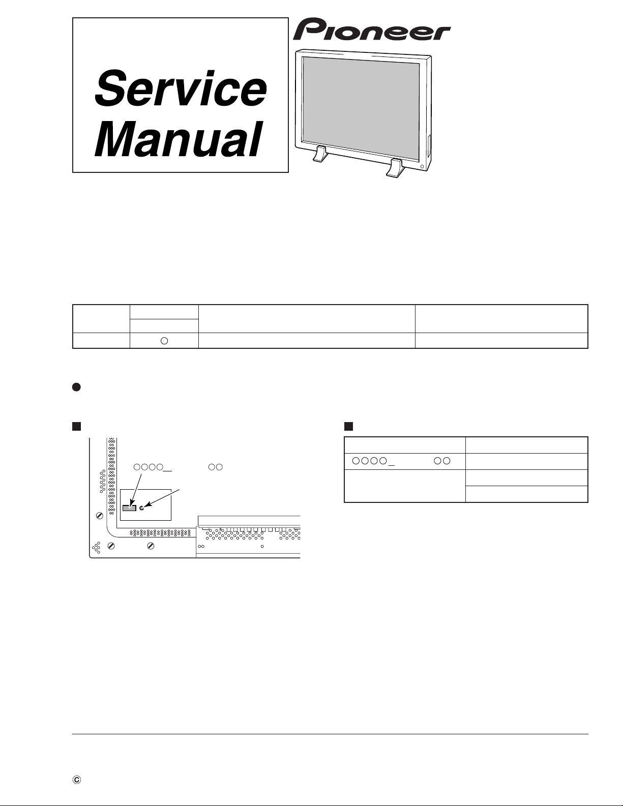
THIS MANUAL IS APPLICABLE TO THE FOLLOWING MODEL(S) AND TYPE(S).
Type
LUBW/CA/1 AC120V
Model
PDP-V402
Note: Pages 26 - 77 and 82 - 89 were intentionally left out.
In PDP-V402, there are two different models (original model and value analysis model).
Confirm the mark and serial No. of the product rear side, and use each service manual.
Power Requirement
Remarks
PRODUCT REAR SIDE
Serial No.
1
(
∗ ∗ ∗ ∗ ∗
Discrimination Seal
(SILVER)
)
SERIAL NO.
Serial No. Service Manual
1 ∗ ∗ ∗ ∗ ∗
OTHER
CONTENTS: See note above for pages left out.
1.SAFETY INFORMATION....................................2
2.EXPLODED VIEWS AND PARTS LIST.............5
3.BLOCK DIAGRAM AND SCHEMATIC DIAGRAM
.......................................................16
4.PCB CONNECTION DIAGRAM.......................90
5.PCB PARTS LIST...........................................133
6.ADJUSTMENT................................................145
7.GENERAL INFORMATION............................152
7.1DIAGNOSIS..............................................152
7.1.1 BURN-IN.........................................152
7.1.2 TROUBLESHOOTING...................154
7.1.3 DISASSEMBLY..............................157
7.1.4 WIRING DIAGRAM........................161
7.2 IC .....................................................166
8.PANEL FACILITIES AND SPECIFICATIONS
.....................................................169
ARP3081 [This manual]
ARP3034
ARP2981 (PDP-V401)
PIONEER CORPORATION 4-1, Meguro 1-chome, Meguro-ku, Tokyo 153-8654, Japan
PIONEER ELECTRONICS SERVICE, INC. P.O. Box 1760, Long Beach, CA 90801-1760, U.S.A.
PIONEER EUROPE NV Haven 1087, Keetberglaan 1, 9120 Melsele, Belgium
PIONEER ELECTRONICS ASIACENTRE PTE. LTD. 253 Alexandra Road, #04-01, Singapore 159936
PIONEER CORPORATION 2000
T–ZZA OCT. 2000 Printed in Japan
Page 2

PDP-V402
1. SAFETY INFORMATION
This service manual is intended for qualified service technicians; it is not meant for the casual
do-it-yourselfer. Qualified technicians have the necessary test equipment and tools, and have been
trained to properly and safely repair complex products such as those covered by this manual.
Improperly performed repairs can adversely affect the safety and reliability of the product and may
void the warranty. If you are not qualified to perform the repair of this product properly and safely, you
should not risk trying to do so and refer the repair to a qualified service technician.
WARNING
This product contains lead in solder and certain electrical parts contain chemicals which are known to the state of California to
cause cancer, birth defects or other reproductive harm.
Health & Safety Code Section 25249.6 – Proposition 65
NOTICE
(FOR CANADIAN MODEL ONLY)
Fuse symbols (fast operating fuse) and/or (slow operating fuse) on PCB indicate that replacement parts
must be of identical designation.
REMARQUE
(POUR MODÈLE CANADIEN SEULEMENT)
Les symboles de fusible (fusible de type rapide) et/ou (fusible de type lent) sur CCI indiquent que les
pièces de remplacement doivent avoir la même désignation.
1.1 SAFETY PRECAUTIONS
NOTICE : Comply with all cautions and safety related notes located
on or inside the cabinet and on the chassis.
The following precautions should be observed :
1. When service is required, even though the PDP UNIT an isolation
transformer should be inserted between the power line and the
set in safety before any service is performed.
2. When replacing a chassis in the set, all the protective devices
must be put back in place, such as barriers, nonmetallic knobs,
adjustment and compartment covershields, isolation resistorcapacitor, etc.
3. When service is required, observe the original lead dress. Extra
precaution should be taken to assure correct lead dress in the
high voltage circuitry area.
4. Always use the manufacture's replacement components.
Especially critical components as indicated on the circuit diagram
should not be replaced by other manufacture's.
Furthermore where a short circuit has occurred, replace those
components that indicate evidence of overheating.
5. Before returning a serviced set to the customer, the service
technician must thoroughly test the unit to be certain that it is
completely safe to operate without danger of electrical shock,
and be sure that no protective device built into the set by the
manufacture has become defective, or inadvertently defeated
during servicing. Therefore, the following checks should be
performed for the continued protection of the customer and
service technician.
6. Perform the following precautions against unwanted radiation
and rise in internal temperature.
• Always return the internal wiring to the original styling.
• Attach parts (Ground, Rear Cover, Shield Case) surely after
disassembly.
7. Perform the following precautions for the PDP panel.
• When the front case is removed, make sure nothing hits the
panel face, panel corner, and panel edge (so that the glass does
not break).
• Make sure that the panel vent does not break. (Check that the
cover is attached.)
• Handle the FPC connected to the panel carefully.
Twisting or pulling the FPC when connecting it to the connector
will cause it to peel off from the panel.
8. Pay attention to the following.
• Be sure to wire the fan. If the fan does not work, the temperature
will rise and cause the protection circuit to operate.
• When the front case is removed, infrared ray is radiated and
may disturb reception of the remote control unit.
• Pay extreme caution when the front case and rear panel are
removed because this may cause a high risk of disturbance to
TVs and radios in the surrounding.
2
Page 3
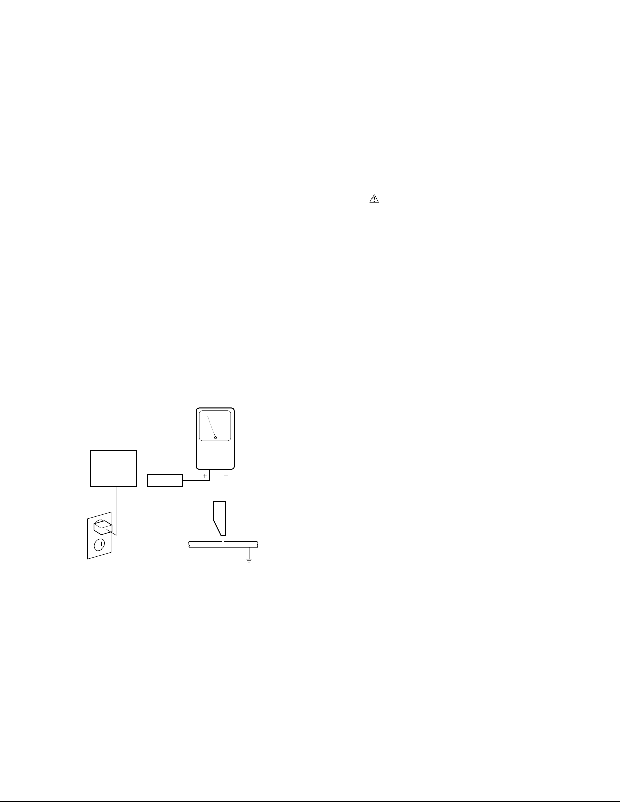
Leakage Current Cold Check
With the AC plug removed from an AC power source, place a
jumper across the two plug prongs. Turn the AC power switch on.
Using an insulation tester (DC 500V), connect one lead to the
jumpered AC plug and touch the other lead to each exposed metal
part (input/output terminals, screwheads, metal overlays, control
shafts, etc.), particularly any exposed metal part having a return
path to the chassis. Exposed metal parts having a return path to the
chassis should have a minimum resistor reading of 0.3MΩ and a
maximum resistor reading of 5MΩ. Any resistor value below or
above this range indicates an abnormality which requires corrective
action. Exposed metal parts not having a return path to the chassis
will indicate an open circuit.
Leakage Current Hot Check
Plug the AC line cord directly into an AC power source (do not use
an isolation transformer for this check).
Turn the AC power switch on.
Using a "Leakage Current Tester (Simpson Model 229 equivalent)",
measure for current from all exposed metal parts of the cabinet
(input/output terminals, screwheads, metal overlays, control shaft,
etc.), particularly any exposed metal part having a return path to the
chassis, to a known earth ground (water pipe, conduit, etc.). Any
current measured must not exceed 0.5mA.
PDP-V402
1.2 PRODUCT SAFETY NOTICE
Many electrical and mechanical parts in PIONEER set have special
safety related characteristics. These are often not evident from
visual inspection nor the protection afforded by them necessarily
can be obtained by using replacement components rated for higher
voltage, wattage, etc. Replacement parts which have these special
safety characteristics are identified in this Service Manual.
Electrical components having such features are identified by marking
with a
Manual.
The use of a substitute replacement component which dose not have
the same safety characteristics as the PIONEER recommended
replacement one, shown in the parts list in this Service Manual, may
create shock, fire or other hazards.
Product Safety is continuously under review and new instructions
are issued from time to time. For the latest information, always
consult the current PIONEER Service Manual. A subscription to, or
additional copies of, PIONEER Service Manual may be obtained at
a nominal charge from PIONEER.
on the schematics and on the parts list in this Service
Reading should
not be above
0.5 mA
Earth ground
Device
under
test
Also test with plug
reversed
(Using AC adapter
plug as required)
Test all exposed
metal surfaces
Leakage
current
tester
AC Leakage Test
ANY MEASUREMENTS NOT WITHIN THE LIMITS
OUTLINED ABOVE ARE INDICATIVE OF A POTENTIAL
SHOCK HAZARD AND MUST BE CORRECTED BEFORE
RETURNING THE SET TO THE CUSTOMER.
3
Page 4
PDP-V402
1.3 CHARGED SECTION AND HIGH VOLTAGE GENERATING POINT
7 Charged Section
The places where the commercial AC power is used without
passing through the power supply transformer.
If the places are touched, there is a risk of electric shock. In addition,
the measuring equipment can be damaged if it is connected to the
GND of the charged section and the GND of the non-charged
section while connecting the set directly to the commercial AC
power supply. Therefore, be sure to connect the set via an insulated
transformer and supply the current.
7 Charged Section
(Power supply primary side)
1. AC Power Cord
2. AC Inlet with Filter
3. Power Switch (S1)
4. Fuse (In the MAIN POWER ASSY)
5. STB Transformer and Converter Transformer
(In the MAIN POWER ASSY)
6. Other primary side of the MAIN POWER ASSY
ANALOG VIDEO ASSY
3D Y/C ASSY
7 High Voltage Generating Point
The places where voltage is 100V or more except for the charged
places described above. If the places are touched, there is a risk of
electric shock.
1. MAIN POWER ASSY ...................................... (170V)
2. X DRIVE (A) ASSY ......................................... (170V)
3. X DRIVE (B) ASSY ......................................... (170V)
4. Y DRIVE (A) ASSY ......................................... (170V)
5. Y DRIVE (B) ASSY ......................................... (170V)
6. SCAN MODULE (A) and (B) .......................... (150V)
For the places, refer to the EXPLODED VIEWS, the SCHEMATIC
DIAGRAM and the PCB CONNECTION DIAGRAM sections.
Part is charged section.
Part is the high voltage generating points other than the
charged section.
X DRIVE (B) ASSY
AC Inlet
Power Switch (S1)
X DRIVE (A) ASSY
MAIN POWER ASSY
Y DRIVE (A) ASSY
SCAN MODULE (B)
SCAN MODULE (A)
Y DRIVE (B) ASSY
4
Page 5
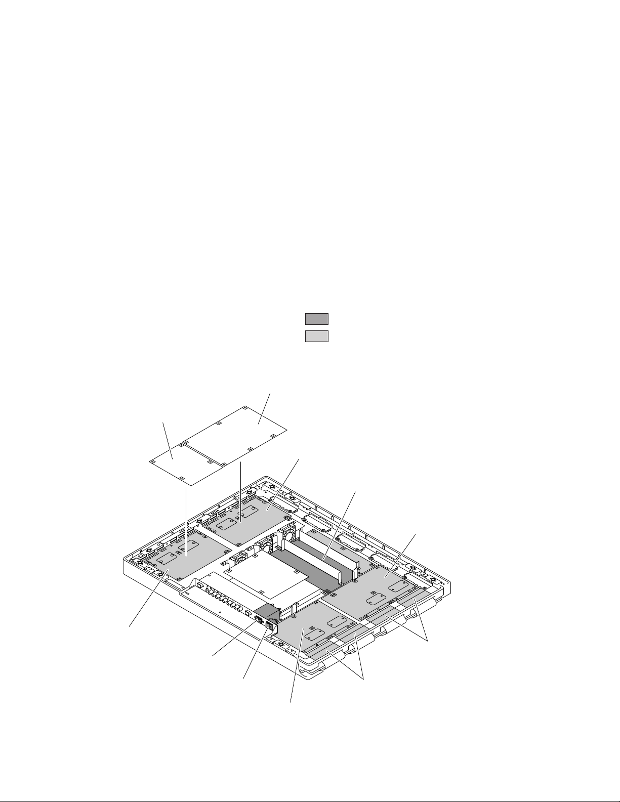
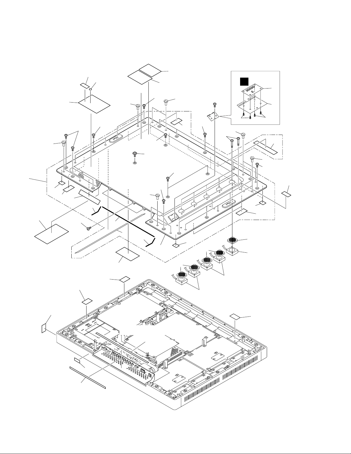
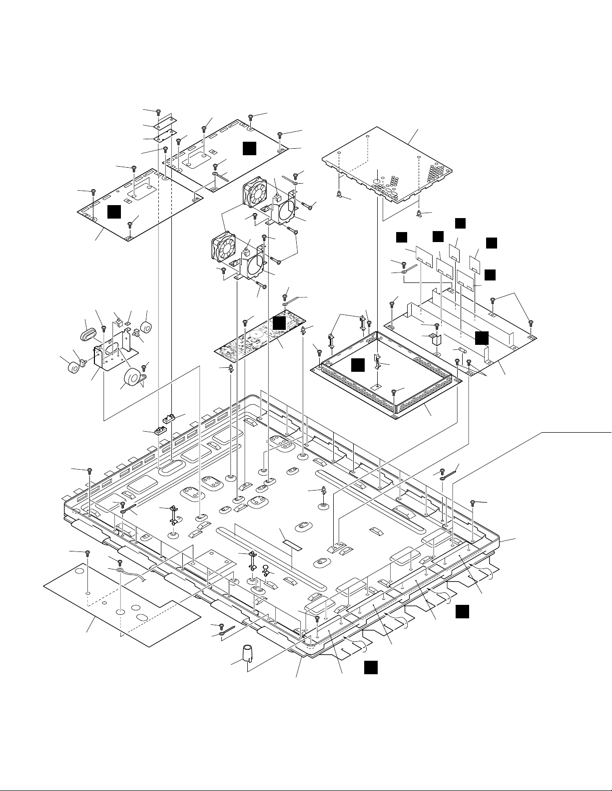
2. EXPLODED VIEWS AND PARTS LIST
NOTES : Parts marked by “ NSP ” are generally unavailable because they are not in our Master Spare Parts List.
The mark found on some component parts indicates the importance of the safety factor of the part.
Therefore, when replacing, be sure to use parts of identical designation.
Screw adjacent to mark on the product are used for disassembly.
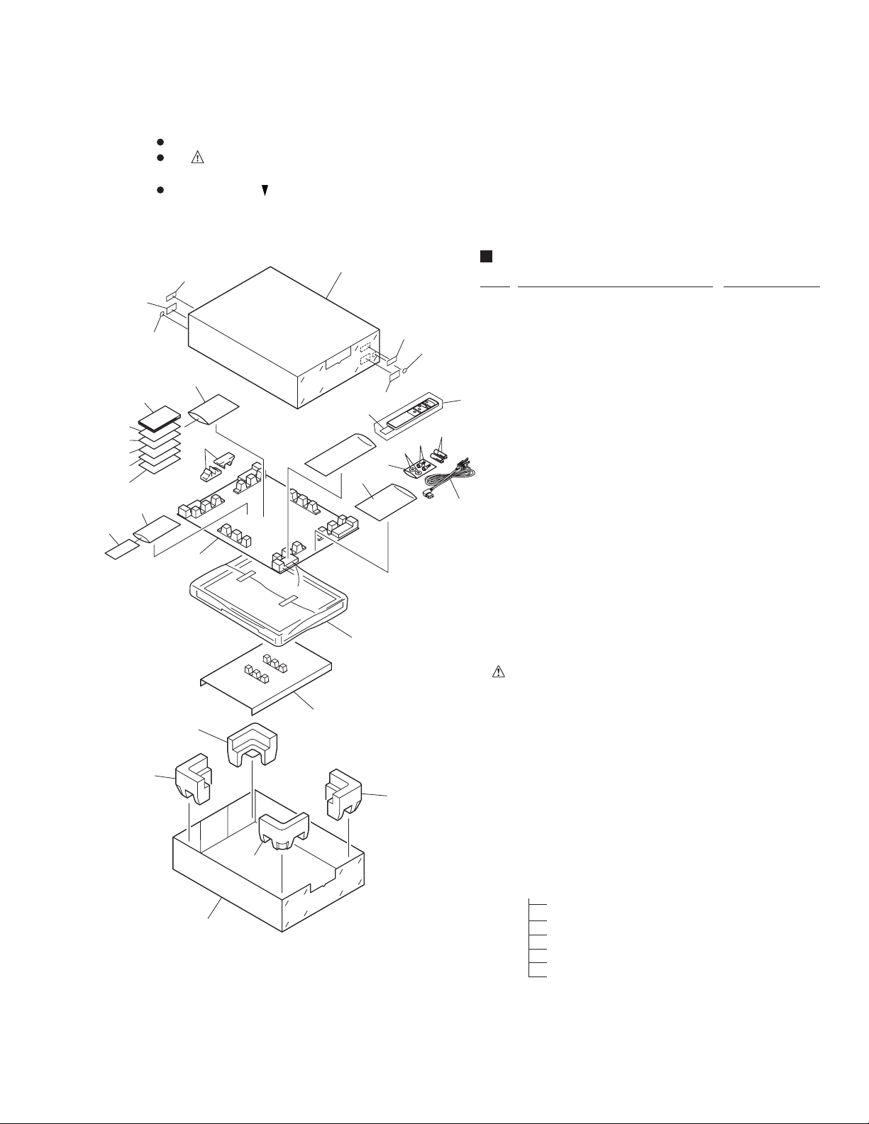
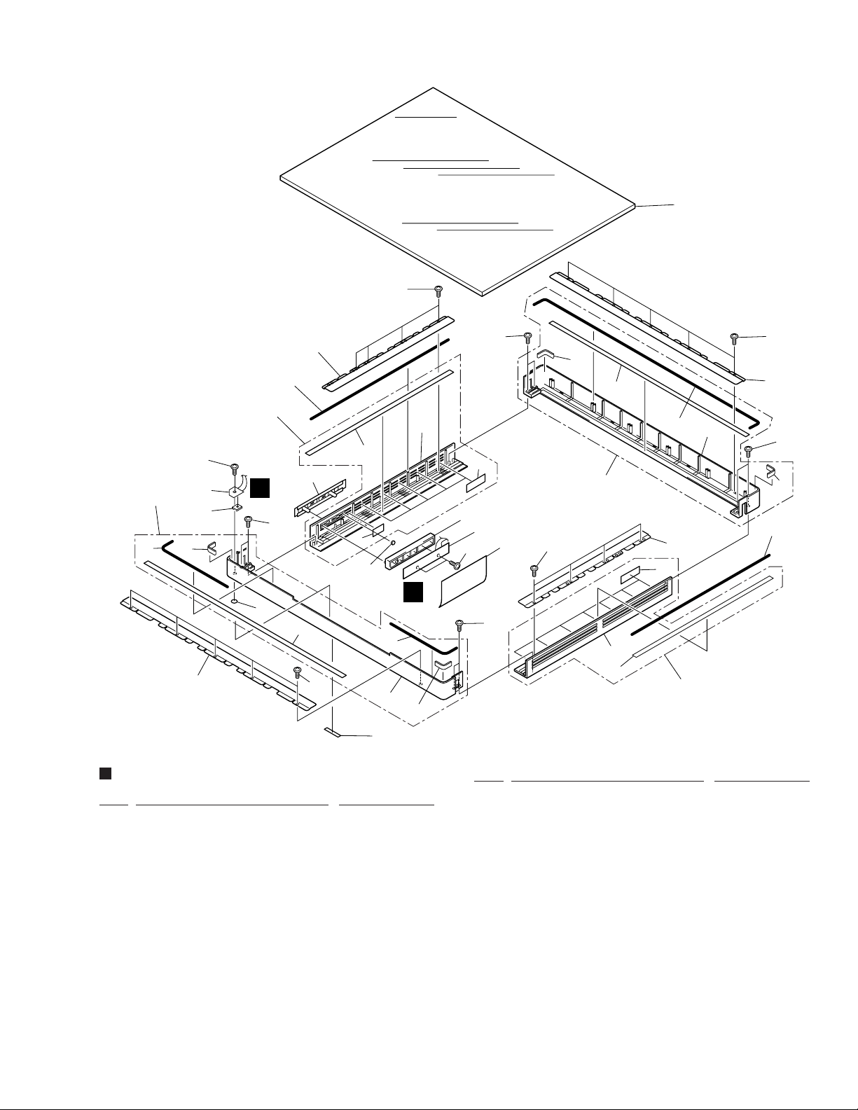
2.1 PACKING
PACKING PARTS LIST
Mark No. Description Part No.
20
6
PDP-V402
29
11
13
12
24
28
27
10
25
30
1 Under Pad A AHA2249
2 Under Pad B AHA2250
20
30
9
27
15
17
23
22
19
9
4
8
3
1
14
16
21
3 Under Pad C AHA2251
4 Upper Pad AHA2252
5 ...............................
6 Upper Carton AHD3052
7 Under Carton AHD3041
8 Mirror Mat AHG1273
NSP 9 Literature Bag AHG-117
10 Operating Instructions ARD1030
(English/Japanese)
11 Plasma Caution Sheet ARM1145
12 Plasma Caution Sheet ARM1147
13 Caution Sheet ARM1169
14 Remote Control Unit AXD1441
(CU-V153)
15 Battery Cover AZN2098
NSP 16 Batteries (R6P, AA) AEX1025
NSP 17 Vinyl Bag AHG-064
18 ...............................
19 Display Stand V AMR3232
20 Packing Label AAX2822
21 AC Power Cord BDG1025
22 Bolt (Hex) SMZ80H350FZB
23 Washer WB80FZB
NSP 24 Warranty Card ARY1102
NSP 25 Vinyl Pouch AHG-195
26 ...............................
2
2
1
7
NSP 27 Label VRW1629
28 Caution Sheet ARM1176
NSP 29 Warranty Card ARY1093
30 Discrimination Seal (SILVER) AAX2817
31 Packing Assy AHF1001
Packing Assy (AHF1001) is composed of the following parts.
31 Packing Assy AHF1001
1 Under Pad A AHA2249
2 Under Pad B AHA2250
3 Under Pad C AHA2251
4 Upper Pad AHA2252
6 Upper Carton AHD3052
7 Under Carton AHD3041
5
Page 6
PDP-V402
2.2 REAR PANEL SECTION
41
14
22
13
12
19
11
23
23
34
16
32
23
15
10
22
16
22
24
23
23
23
6
40
39
23
22
12
13
23
K
9
7
8
22
26
13
5
5
4
8
11
22
23
17
12
33
28
31
28
Refer to " MAIN UNIT SECTION (1/3)".
1
29
2
5
4
4
30
6
Page 7

REAR PANEL SECTION PARTS LIST
Mark No. Description Part No.
1 Label RS AAX2744
2 Label TP AAX2729
3 ...............................
4 Fan Motor (60×15) AXM1039
5 Fan Guard ANG2418
6 Rear Cover Assy ANE1572
7 PCB Cover ANG2186
8 Circuit Board Spacer AEC1862
9 FAN RELAY ASSY AWZ6535
10 Net RA AED1170
11 Net RC AED1171
12 Net FA AED1165
13 Net FB AED1184
14 Insulating Sheet R AEC1823
15 Shield Gusket E ANK1657
16 Shield Gusket D ANK1674
17 Cable Clamp Label ARW1076
18 ...............................
NSP 19 Label AAL2337
20 ...............................
21 ...............................
22 Hole Rivet AMR2969
23 Screw PMB30P080FZK
24 Screw ABA1283
25 ...............................
PDP-V402
26 Screw PPZ50P100FZK
27 ...............................
28 Cover Sheet AEC1824
29 Serial Seal AAX2732
NSP 30 Drive Voltage Label ARW1097
31 Solder Warning Label AAX2644
32 Discrimination Label (SILVER) AAX2816
33 Display Label AAX–359
NSP 34 Label VRW1629
35 ...............................
36 ...............................
37 ...............................
38 ...............................
NSP 39 Bolt Caution Label AAX2630
40 Cleaning Label AAX2751
41 Rear Cover Service Assy AEA1036
7
Page 8
PDP-V402
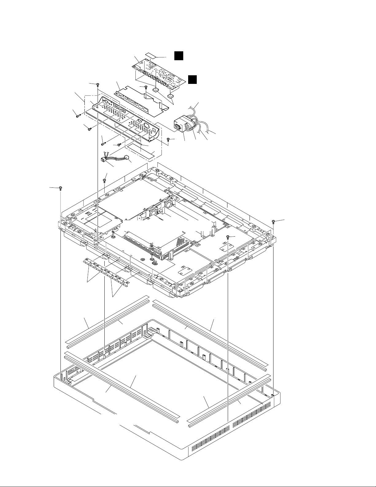
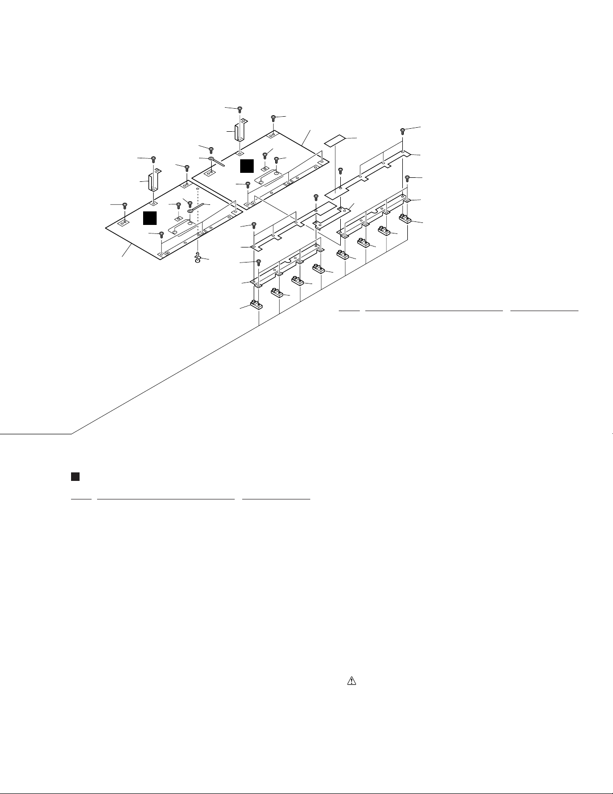
2.3 MAIN UNIT SECTION (1/3)
10
24
6
4
5
3
7
25
26
6
10
5
1
Refer to " MAIN UNIT SECTION (2/3)".
11
13
17
21
27
L
5
A
12
18
14
2
15
10
10
22
22
8
20
9
19
19
9
8
20
Refer to " FRONT PANEL SECTION ".
8
Page 9

MAIN UNIT SECTION (1/3) PARTS LIST
Mark No. Description Part No.
1 Power Switch (S1) BSM1010
2 AC Inlet with Filter (CN1) AKP1211
3 Inlet Panel ANG2425
4 INPUT CONTROL Assy AWZ6554
5 Screw PMB30P080FZK
6 Screw BBA1017
7 Screw BPZ30P080FZK
NSP 8 Panel Sheet V AMR3154
NSP 9 Panel Sheet H AMR3172
10 Screw BPZ40P080FZK
11 Shield Gusket C ANK1655
12 Ground Wire (J50) ADX2332
13 2P Housing Wire (J51) ADX2584
14 Ferrite Core (L1) ATX1032
15 Wire (J53) ADX2586
16 Screw BBZ30P080FZK
17 Net RC AED1171
18 Wire (J52) ADX2585
19 Panel Cushion H AED1179
20 Panel Cushion V AED1180
PDP-V402
21 SYNC DET ASSY AWZ6548
22 Front Shield ANK1672
23 ...............................
24 Inlet Panel Service Assy AEA1048
25 Shield Sheet I/O ANK1675
26 Screw PMB30P060FCU
27 Cushion AEB1340
9
Page 10
PDP-V402
2.4 MAIN UNIT SECTION (2/3)
C
21
6
9
B
19
21
4
Q
23
22
20
3
14
18
19
19
12
7
19
7
2
20
20
5
24
1
10
20
1
15
1
20
17
B
17
B
16
19
18
19
12
12
19
19
12
19
12
18
19
19
19
12
19
12
19
12
19
19
12
18
19
MAIN UNIT SECTION (2/3) PARTS LIST
Mark No. Description Part No.
1 FPC Cushion AEB1343
NSP 2 PCB Angle A ANG2162
NSP 3 PCB Angle B ANG2163
4 3D Y/C ASSY AWQ1055
5 Shield Sheet ANK1669
6 ANALOG VIDEO ASSY AWQ1056
7 PCB Hinge AEC1694
8 ...............................
9 CONTROL ASSY AWZ6545
10 Rivet AEC1658
19
13
Refer to " MAIN UNIT SECTION (3/3)".
Mark No. Description Part No.
11 ...............................
12 FPC Shield H ANK1518
13 Angle D ANG2252
14 Angle B Service Assy AEA1046
15 Angle B ANG2434
16 Angle A ANG2250
17 Screw PMB30P080FZK
NSP 18 Corner Angle ANG2158
19 Screw ABA1266
20 Screw IBZ30P080FCC
21 Screw BMZ30P080FMC
22 Ferrite Core (L2) ATX1032
23 Ferrite Core (L3) ATX1031
24 Binder AEC1851
15
10
Page 11
J
I
13
16
16
16
16
15
21
29
15
14
8
8
7
6
4
3
17
2
25
26
18
27
10
12
14
22
8
8
5
23
24
31
27
11
19
8
2
1
21
17
28
8
27
27
19
30
20
9
2.5 FRONT PANEL SECTION
PDP-V402
FRONT PANEL SECTION PARTS LIST
Mark No. Description Part No.
NSP 1 Front Case C AMB2605
2 Net FA AED1165
NSP 3 Front Case D AMB2606
4 Net FB AED1184
5 Control Name Plate AAK2706
6 LED Lens AAK2695
7 Control Button AAC1536
8 Screw BPZ30P080FZK
9 Front Case A AMB2603
10 Front Case B AMB2608
11 Lens AAK2698
12 Pioneer Seal ARW1088
13 Protect Panel Assy AMR3229
NSP 14 Panel Spacer A ANG2155
NSP 15 Panel Spacer B ANG2156
Mark No. Description Part No.
16 Screw BPZ40P080FZK
17 Shield Gusket B ANK1654
18 Shield Gusket H ANK1660
19 Shield Gusket A ANK1653
20 Shield Gusket F ANK1658
21 Shield Gusket G ANK1659
22 Shield Gusket I ANK1661
23 IR RECEIVER ASSY AWZ6526
24 Cushion Rubber AEB1336
25 FRONT KEY ASSY AWZ6525
NSP 26 Shield Sheet ANK1532
27 Cushion AEB1342
28 Front Case C Service Assy AEA1030
29 Front Case D Service Assy AEA1031
30 Front Case A Service Assy AEA1034
31 Front Case B Service Assy AEA1035
11
Page 12
PDP-V402
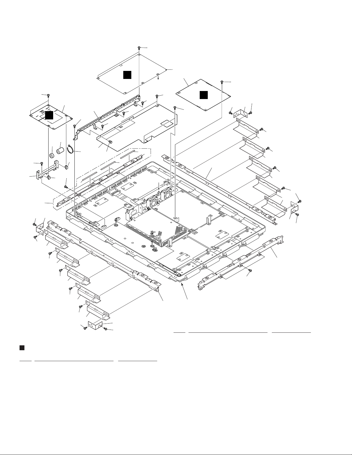
2.6 MAIN UNIT SECTION (3/3)
55
54
17
18
19
5
16
5
5
F
15
5
39
38
40
56
53
55
54
5
16
5
5
6
12
5
10
5
5
11
N
14
5
6
13
11
5
13
5
6
10
5
20
34
23
5
E
40
5
40
13
5
D
22
23
U
49
R
46
5
6
5
33
S
47
50
V
T
48
5
9
51
5
M
5
5
21
8
8
5
10
5
5
4
3
2
44
6
44
5
6
1
45
7
5
24
O
27
24
28
6
5
5
5
26
25
P
25
12
Page 13
PDP-V402
5
29
5
5
29
5
5
H
5
35
6
5
16
6
52
G
5
17
31
5
32
8
5
36
5
16
8
8
37
30
8
8
8
17
31
5
32
8
8
Mark No. Description Part No.
21 MAIN POWER ASSY AWR1077
22 Shield Case B ANK1517
23 PCB Spacer AEC1121
24 SCAN MODULE (A) AXF1104
25 SCAN MODULE (B) AXF1105
NSP 26 Aluminium Panel ANA1555
NSP 27 Plasma Panel Assy AAV1235
28 DIGITAL VIDEO ASSY AWP1069
NSP 29 Rear Panel Angle ANG2171
NSP 30 Hot Plate B ANG2160
MAIN UNIT SECTION (3/3) PARTS LIST
Mark No. Description Part No.
NSP 1 Pipe Cover AMR2935
2 Terminal Shield ANK1547
3 Ground Wire (J50) ADX2332
4 Screw FBT40P080FZK
5 Screw IBZ30P080FCC
6 Binder AEP-215
7 Insulating Sheet S AEC1822
8 Plate Spacer AMR3068
NSP 9 PCB Holder D ANG2165
10 Circuit Board Spacer AEC1696
NSP 11 Fan Angle ANG2166
12 Fan Motor (60×25) AXM1038
13 Screw PPZ50P100FZK
14 X DRIVE (A) ASSY AWP1078
15 X DRIVE (B) ASSY AWP1079
16 Screw BBZ30P140FMC
17 Screw ABZ30P100FMC
18 Barrier S AEC1821
NSP 19 Hot Plate S ANG2161
20 SUB POWER ASSY AWZ6173
31 Barrier L AEC1820
NSP 32 Hot Plate A ANG2159
33 Circuit Board Spacer AEC1720
34 R Free Spacer AEC1721
35 Y DRIVE (B) ASSY AWP1077
36 Y DRIVE (A) ASSY AWZ6533
37 Caution Label ARW1073
NSP 38 Core Holder ANG2433
39 Bush C AEC1740
40 PCB Hinge AEC1694
41 Shield Case B ANK1517
NSP 42 PCB Spacer AEC1121
43 ...............................
NSP 44 PCB Spacer AEC1104
45 Card Spacer AEC1706
46 RCC CONTROL (A) ASSY AWZ6174
47 RCC CONTROL (B) ASSY AWZ6175
48 RCC CONTROL (C) ASSY AWZ6176
49 OTL CONTROL (A) ASSY AWZ6177
50 OTL CONTROL (B) ASSY AWZ6178
51 Fuse (8A, FU1) REK1086
NSP 52 Spacer AEC1074
53 Insulation Rear Sheet AEC1866
54 Ferrite Core Holder AEC1818
55 Ferrite Core (L5, L6) ATX1037
56 Ferrite Core (L4) ATX1042
13
Page 14

PDP-V402
2.7 PDP SERVICE ASSY (AWU1026)
PDP SERVICE ASSY (AWU1026) is composed of the following parts.
Please refer to 2.1.2 to 2.1.4 and 2.1.6 for the illustrations of each part.
Mark No. Description Part No. Mark No. Description Part No.
2.1 REAR PANEL SECTION
28 Cover Sheet AEC1824
NSP 30 Drive Voltage Label ARW1097
2.3 MAIN UNIT SECTION (1/3)
NSP 8 Panel Sheet V AMR3154
NSP 9 Panel Sheet H AMR3172
2.4 MAIN UNIT SECTION (2/3)
1 FPC Cushion AEB1343
12 FPC Shield H ANK1518
13 Angle D ANG2252
15 Angle B ANG2434
16 Angle A ANG2250
NSP 18 Corner Angle ANG2158
19 Screw ABA1266
2.6 MAIN UNIT SECTION (3/3)
NSP 1 Pipe Cover AMR2935
5 Screw IBZ30P080FCC
7 Insulating Sheet S AEC1822
10 Circuit Board Spacer AEC1696
NSP 26 Aluminium Panel ANA1555
NSP 27 Plasma Panel Assy AAV1235
NSP 44 PCB Spacer AEC1104
45 Card Spacer AEC1706
OTHERS
NSP Address Module (A) MC-8795A-A
NSP Address Module (B) MC-8795B-A
NSP
NSP
NSP
NSP
Flexible Print Cable (A) (J65, J66)
Flexible Print Cable (B) (J67, J68)
Flexible Print Cable (A) (J77, J78)
Flexible Print Cable (B) (J79, J80)
BS Panel Label AAX2745
ADY1033
ADY1034
ADY1041
ADY1042
PACKING
NSP Corner Pad AHA2207
NSP Upper Carton AHD2968
NSP Under Carton AHD2969
NSP Holder Plate AHK1007
Button Bolt ABA1259
Packing Sheet AHG1291
Washer WB80FZB
14
Page 15

PDP-V402
15
Page 16
1
23
PDP-V402
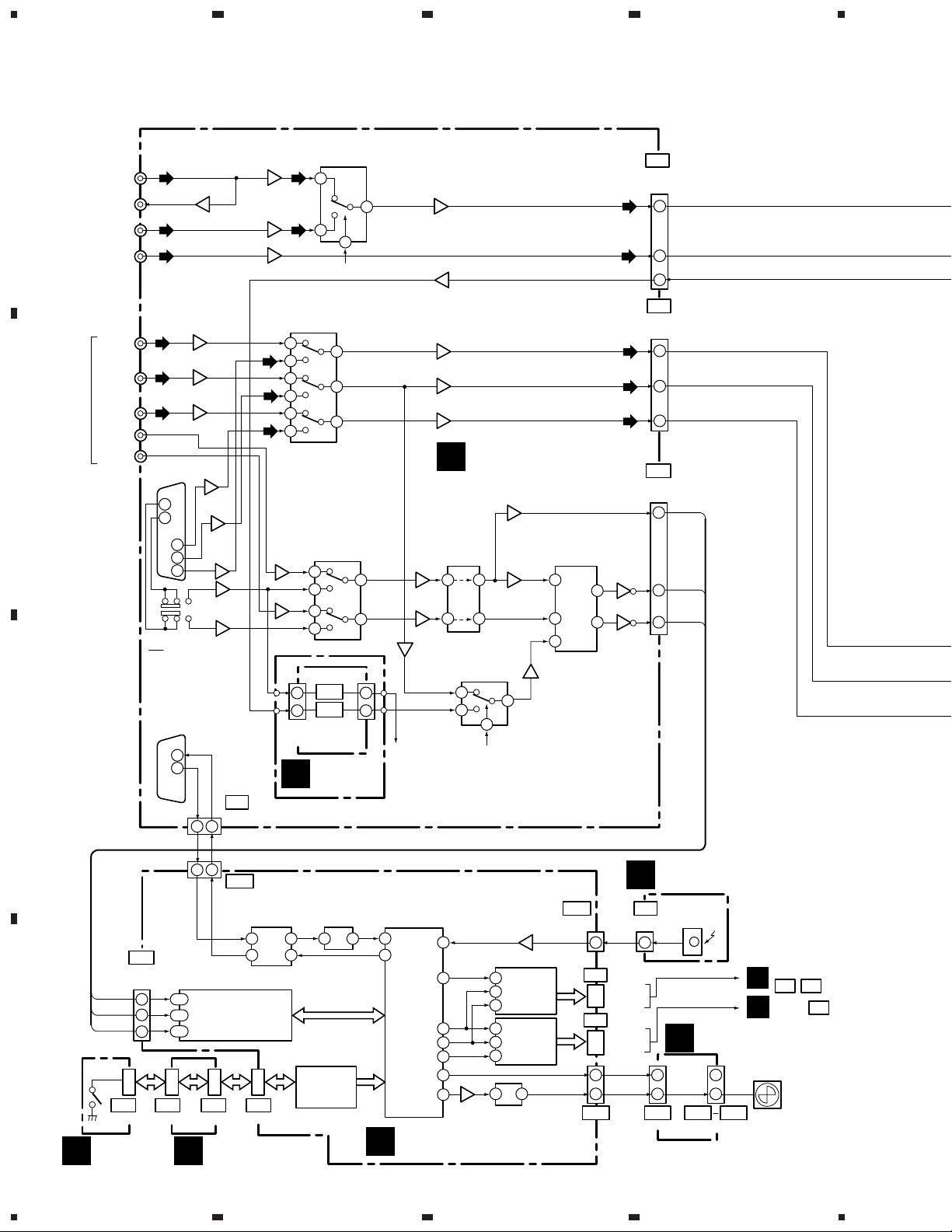
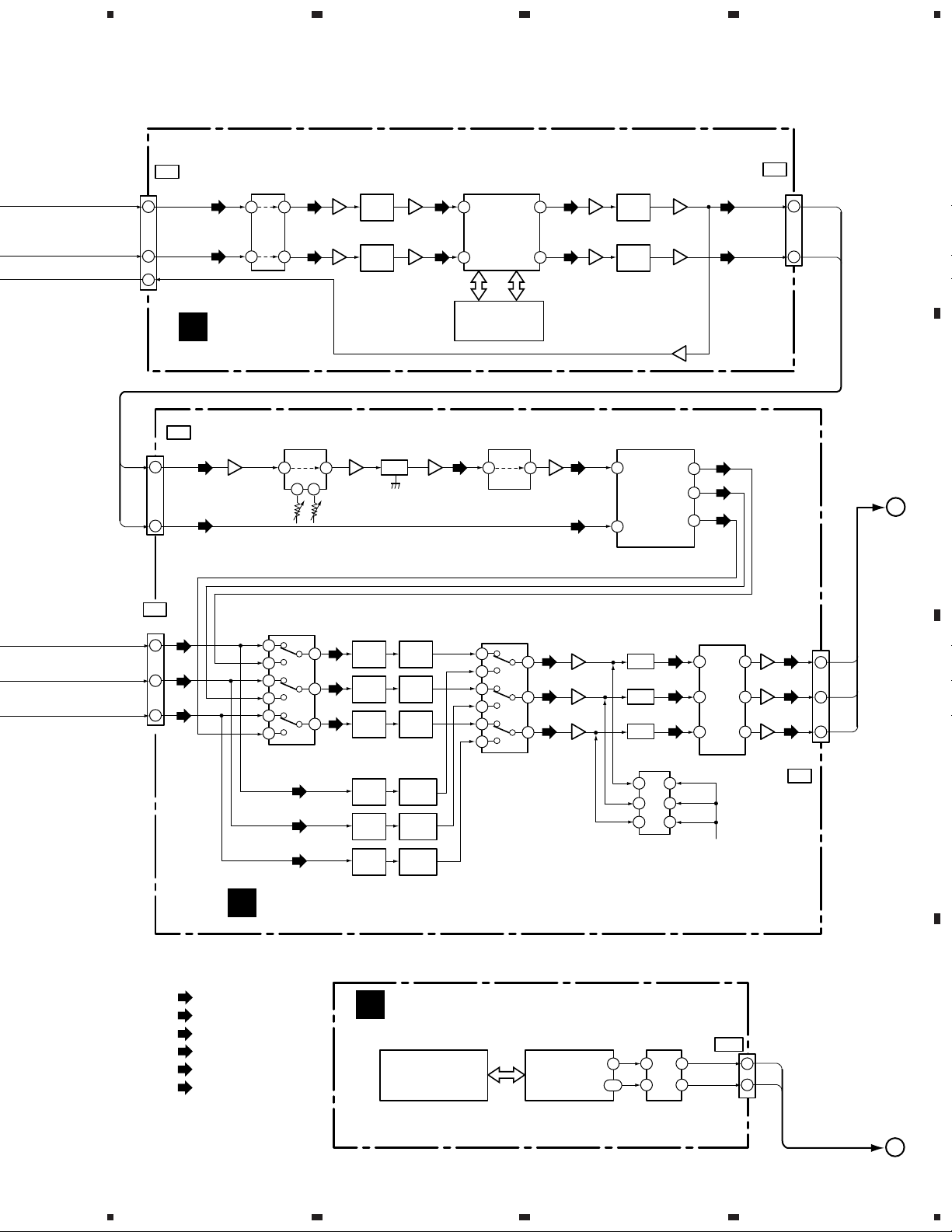
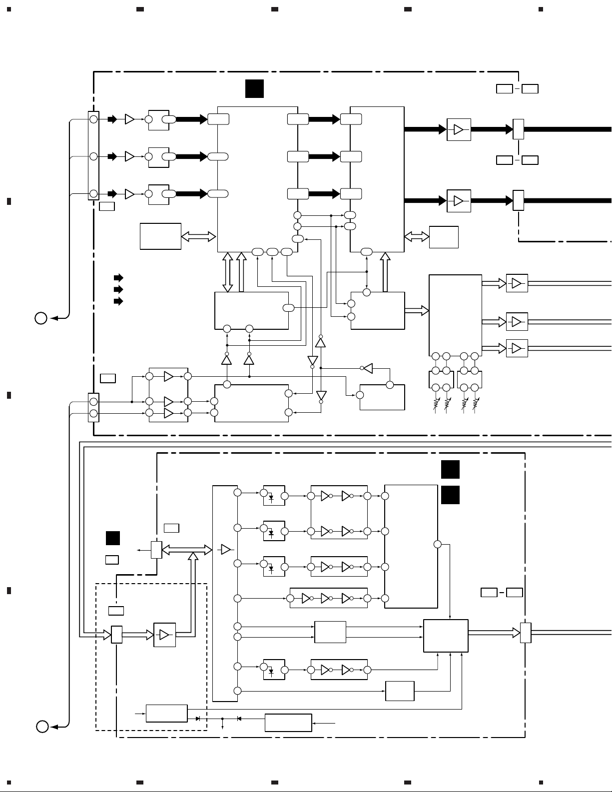
3. SCHEMATIC DIAGRAM AND BLOCK DIAGRAM
3.1 BLOCK DIAGRAM
IC1005
A
C. VIDEO
IN
C. VIDEO
OUT
RED
GREEN
RGB1
BLUE
HD/CS
B
VD
RGB2
Y
C
(V)
(Y)
(C)
(R)
(G)
(B)
CN1203
14
13
3
2
1
S1201
ON – OFF
Q1029-Q1033
Q1201
Q1202
Q1203
Q1204
Q1205
B
G
Q1206
R
HD
VD
Q1034
Q1028
Q1027
(R)
(G)
(B)
Q1038
Q1039
STD_Y
CN1006
TXD
2
RXD
C
RS-232C
3
G6
CN1007
4 3
RXD
TXD
4 3
M11
CN7003
IC7003
MC145407F
RXD
9
TXD
8
RS-232C
RECEIVER/DRIVER
IC7502
CPLD
CN7351
INHSYNC
INVSYNC
HD
M5
(14P)
6
8
11
122
120
EPM7256AETC144-10
113
D
M6
G8
G7
F1
CN7800
FRONT KEY
I
ASSY
CN1005
A
CN7000
CN1004
INPUT CONTROL
ASSY
NJM2233BLA
(V)
(Y)
IC1201
TC4053BF
1
2
3
5
13
12
TC4053BF
Q1040
Q1041
Q7750-Q7752
RGB2_HD
3
C
6
F
Q7753,Q7754
(8P)
CN7750
L
(4P)
(4P)
TC7566FU
13
IC7000 PD5136
KEY INPUT
MICRO-
COMPUTER
6
4
8
7
Y/C SW
15
4
14
IC1001
1
2
3
5
DET
LPF
HD
15
VD
4
4
7
SYNC DET
ASSY
SYSTEM CONTROL
IC7004
MICROCOMPUTER
1212
B
Q1035
Q1037
Q1207
Q1208
Q1209
A
INPUT CONTROL ASSY
COMP.
IC1002
Q1001-
NJM319M
Q1004
4 4
Q1005-
Q1008
9127
Q1036
D
G
RGB2_DET
IC7002
M38869FFAHP
RXD/SDA2
21
20
TXD
OSD_CEB
DAC_CEB
CONTROL ASSY
NJM2233BLA
BNC_G
SYNC_Y
REM_IN REM
22
46
CLK
7
DATA
8
47
PD
15
FAN
14
IC1006
6
8
CN. SW
PQ20VZ1U
Q1010
Q1009
4
7
4
5
PD5385A
6
2
3
M62358FP
1
4 3
IC7900
VIDEO
IC7253
OSD
IC7252
DAC
HD
IN
VD
IN
IN
SYNC
PROCESSOR
IC1004
CXA1616S
18
1
21
7
Q1045
M12
CN7001
(3P)
1 3
M7
M4
2
CN7901
1
(3P)
M19 FR1 FR2 FR6
G2
CN1002
(8P)
(V/Y)
(C)
V/Y
3
C
5
3DY
1
G1
CN1201
(6P)
(R)
(G)
(B)
R OUT
1
G OUT
3
B OUT
5
G4
CN1001
(14P)
HD
11
INPUT
HSYNC
6
INPUT
VSYNC
8
IR RECEIVER
J
ASSY
X7850
H1
REMOTE
CN7850
CN7251
(11P)
CN7250
(10P)
P.D
12V/8.8V
SENSOR
(3P)
K
2
1
CN5801 CN5802-CN5806
4
J2202
C
A2 A8
J2601
C
FAN RELAY ASSY
2
1
FAN
A6
16
1234
Page 17
5
678
PDP-V402
V/Y
C
3DY
3D_Y
3D_C
CN2401
R SIG
G SIG
B SIG
B2
CN3203
(8P)
3
5
1
A1
CN2201
(4P)
1
3
(6P)
A5
(R)
1
(G)
3
(B)
5
VIDEO AMP
IC3204
TK15420M
(V/Y)
(C)
Q
(Y)
(C)
5 7
3
1
3D Y/C ASSY
BLACK LEVEL
CONTROL
Q2801-Q2803 Q2811
IC2801 PA0028
17
RGB SELECT
IC2401
NJM2283M
1
16
14
11
9
8
(R)
(G)
(B)
Q3206 Q3205
(V/Y)
Q3210 Q3209
(C)
12
5 6
(R)
3
(G)
5
(B)
6
F3201
LPF
F3202
LPF
DELAY
DL2802
Q2403-Q2426
10dB
AMP
10dB
AMP
10dB
AMP
10dB
AMP
10dB
AMP
10dB
AMP
UPD64082GF-3BA
(V/Y)
(C)
MA0-8 MO0-15
Q2813
(Y) (Y)
6MHz
LPF
6MHz
LPF
6MHz
LPF
16MHz
LPF
16MHz
LPF
16MHz
LPF
IC3205
88 84
AY1
AY0
3D Y/C SEP.
AC1
96 83
MSM5416258B-30JD
IC2802 PA0030
RGB SELECT
AC0
4M DRAM
IC3206
SHARPNESS
CONTROL
7 58
9
Q2814
IC2402
NJM2283M
1
16
14
11
9
8
(R)
3
(G)
5
(B)
6
Q3224
(Y)
Q3217
(C)
(C)
Q2648,Q2629
Q2649,Q2627
Q2650,Q2631
F3203
Q3220,Q3223
LPF
F3205
Q3214,Q3218
LPF
Q3208
RGB DECODE
IC2201 TA8759BN
Y
C
20
Q2607-Q2610
41
R OUT
G OUT
42
B OUT
43
IC2601 M51387P
(R)
OSD
Q2611-Q2614
(G)
OSD
Q2615-Q2618
(B)
OSD
1
5
3
6
8
13
IC2602
TC74HC4066AF
PEDESTAL CLAMP
(Y)
(C)
(R)
(G)
(B)
RGB AMP
IN
OUT
3
R
R
IN
OUT
7
G
G
IN
OUT
11
B
B
CLAMP PULSE
B4
CN3204
(4P)
Q2651
29
Q2652
25
Q2653
21
3D_Y
1
3D_C
3
(R)
(G)
(B)
CN2602
(7P)
A7
A
B
A
R OUT
1
G OUT
3
B OUT
5
C
(V/Y)
: V/Y Signal Route
(Y)
: Y Signal Route
(C)
: C Signal Route
(R)
: R Signal Route
(G)
: G Signal Route
(B)
: B Signal Route
ANALOG VIDEO ASSY
C
CONTROL ASSY
B
IC7002
M38869FFAHP
SYSTEM CONTROL
MICROCOMPUTER
IC7502
EPM7256AETC144-10
98
HD OUT
CPLD
VD OUT
100
IC7501
TD74BC541F
3217
18
M10
CN7501
(18P)
HD
9
VD
11
D
B
17
5
6
7
8
Page 18
1
PDP-V402
23
4
A/D CONVERTER
A
R IN
G IN
B IN
(R)
1
(G)
3
(B)
5
MB40C558PF
Q6101
MB40C558PF
Q6102
MB40C558PF
Q6103
IC6101
4-11
RV(0-7)
21
IC6105
21
GV(0-7)
4-11 165-172
IC6106
4-11
BV(0-7)
21
153,154,
158-163
174-181
E5
CN6101
(7P)
(R)
(G)
B
(B)
A
E3
CN6104
(18P)
HD
9
VD
11
IC6206
PDY055A
EPLD
: R Signal Route
: G Signal Route
: B Signal Route
IC6001
TC74ACT541FT
7
8
9
UD
AYW1006
MICROCOMPUTER
89
4
IC6008
VD OUT
76
77
3
81
HD IN
VD IN
13
12
11
DIGITAL VIDEO ASSY
D
89-92,
94-100
73-77,
IC6201
PD4800A
GAMMA
193 192 188
HD
UAD
80-85,87
59-64,
66-71
SDT
55
SCK
57
CLK2I
184
VD
REF_H
IC6601
REF_H
GCLK
100
13
IC6005IC6005
12
80
83
PANEL
88
HDVD
10
11
IC6006
PDY053A
EPLD
RD(0-11)
GD(0-11)
BD(0-11)
12
13
5
6
236-246,
249
250-256,
258-262
263,264,
269-278
281
280
SPR
SCK
87
PD4799A
SDT
88
IC6005:
IC6007
IC6007: TC74VHCU04FT
IC6008:
IC6007
21
IC6007
4
TLC2932IPW
IC6301
PD4801A
SFMC
287
92
IC6501
DRVC
TC74VHC04FS
TC74ACT04FT
VCO
FIN_A
OUT
PLL
IC6003
UPPER
ADDRESS
DATA
(0-29)
LOWER
ADDRESS
DATA
(0-29)
3
IC6705-IC6708
TC74ACT541FT
IC6701-IC6704
TC74ACT541FT
DRAM
(×4)
IC6401-IC6404
LC32V4265JL-25S
IC6551
PDY054A
EPLD
21 22
25 27
5 7
5 7
IC6555IC6554
2 14
2 14
VR6553
VR6552
VR6551
SUSTAIN PULSE ADJ
E11 E15
CN6701
CN6705
(18P)
E16 E20
CN6706
CN6710
(18P)
IC6553
TC74ACT541FT
IC6556
TC74ACT540FT
IC6552
TC74ACT541FT
IC6554,IC6555
TC74HC4538AFT
DUAL MMV
VR6554
|
|
PHOTO COUPLER
BUS BUFFER
IC4009
TC74HC541AF
C
(17P)
X9
F
CN4009
CN4009
X9
X4
CN4008
IC4008
TC74HC541AF
BUS BUFFER
(18P)
X DRIVE (A)
ASSY ONLY
D
T4001,IC4007
D-D CONV.
VSUS
(170V)
B
BLOCK
D4010
P.D
IC4012-IC4014,IC4020:
HCPL-M611
IC4012
18
1
IC4013
17
1
IC4014
16
1
SUS-G
15
INA
14
INB
13
IC4020
12
1
XCP
11
VRN(-180V)
D4017
P.D CIRCUIT
IC4005
SUS-B
5
SUS-U
5
SUS-D
5
IC4015
1 12 21
TC74AC04F
3 10 4
1 12 5
IC4022
TC74AC04F
1 12 14
TC74AC04F
RESET
IC4023
TC74AC04F
1 12
5
VCP+12V
Q4001
VCP+12V
IC4017
STK795-120C
PDP PULSE
MODULE
Q4005,Q4007
Charge
Pump
E
F
SUS OUT
7
SUS-MSK
(BYPASS)
CIRCUIT
X DRIVE (A)
ASSY
X DRIVE (B)
ASSY
X12 X17
CN4012
|
CN4017
(8P)
18
1234
Page 19
5
678
PDP-V402
E6
CN6551
(18P)
E8
CN6553
(32P)
E7
CN6552
(20P)
Y4
CN5007
G
CN5009
Y9
Y DRIVE (A) ASSY
G
BUS BUFFER
IC5010
TC74HC541AF
(16P)
(17P)
Y9
CN5009
ADDRESS MODULE (B)
PLASMA
PANEL ASSY
ADDRESS MODULE (A)
H
PHOTO COUPLER
IC5027-IC5032
HCPL-M611
1
5
PHOTO COUPLER
BUS BUFFER
IC5009
TC74HC541AF
IC5017,IC5018,IC5023-IC5025:
HCPL-M611
IC5025
18
1
IC5024
17
1
IC5023
16
1
O P
SCAN MODULE
(A), (B)
Y DRIVE (B) ASSY
BUS BUFFER
IC5019
TC74HC541AFT
IC5014
TC74AC04F
1 12 4
5 10 5
IC5015
TC74AC04F
1 12 14
5
5
5
SUS-B
SUS-U
SUS-D
IC5037
STK795-120C
PDP PULSE
MODULE
CN5013
CN5011
SUS OUT
7
A
Y11
(15P)
Y13
(15P)
B
Y5
CN5008
BUS BUFFER
IC5008
TC74HC541AF
(20P)
Y DRIVE (B)
ASSY ONLY
HDF-0505S
VCC
D-D CONV.
(5V)
T5001,IC5007
D-D CONV.
VSUS
(170V)
Y DRIVE (A)
ASSY ONLY
BLOCK
15
PR-U
14
SEL-H
13
SEL-L
12
VH OVER VOLTAGE DET.
VH UNDER VOLTAGE DET.
SUS-G
Q5007
IC5017
1
IC5018
1
IC5022
TC74AC04F
1 12 21
VSUS170V
Q5006
IC5020,IC5026
5
FET
DRIVER
IC5021,IC5038
5
FET
DRIVER
D5024D5020
D5021D5044
P.D
Q5012
CURRENT
DET.
VCSP(=VOFS)
CSP.GND
(=VOFS-VCSP)
VCP+12V
P.D DET.
Q5001
Q5008
Q5009
PLUS RESET
BLOCK
CN5010
CN5012
C
Y12
(7P)
Y14
(7P)
D
19
5
6
7
8
Page 20
PDP-V402
A
1
CONTROL BLOCK
CONTROL ASSY
B
VCCD5V (5V)
VCCAF12 (12V)
IC7500
1 3
PQ3DZ13
IC7654
3 1
UPC78L05T
23
1 2
IC7653
TC74ACT04FT
2
2
UPC1379C
LPF
IC7652 (1/2)
TC74HC4538
IC7652 (2/2)
TC74HC4538
IC7503 (1/2)
TC74HC4538
IC7503 (2/2)
TC74HC4538
IC7506
TC7WU04FU
9
IC7650
VCO
125
CLK_13M
AFC_VOUT
60
AFC_VIN
62
13
AFC_HIN
66
11
AFC_RETH
56
NTSC_PAL
72
3
128
AFC_CLK
68
5
NTSC_CS2
70
9
CS_REJ
11
10
CP
140
142
CP_1US
H_SYNC1
6
5
H_SYNC2
7
2
IC7502
EPM7256AETC144-10
CPLD
PFD_MUTE
CP_VIDEO
VP_MUTE
VCCPLD (3.3V)
VCCAF05 (5V)
X7500
ASS1128
TCK
TDO
TMS
FIL_1
FIL_2
SELECT
HD_OUT
VD_OUT
RET_HD
RET_VD
OSD_HD
OSD_VD
TDI
104
100
102
106
4
89
20
4
84
87
91
96
98
44
42
46
48
IC7504 (1/2)
TC74HC4538
B
A
CN1001
INHSYNC
INVSYNC
CLP
HP
HEXIT
SYNC_ST
RGB_SW
CN7351
HD
M5
IC7504 (2/2)
TC74HC4538
6
8
10
11
13
14
4
2
10
HD
5
138
/HD_OUT
134
122
HD_SEP
120
VD_SEP
118
CP_SEP
113
HD_COMP
HP_SEP
111
HEXT_SEP
109
25
SYNC_ST
116
RGB_SW
NTSC
MAC
VGA60_75
V_MUTE
FR_SEL
PAL/NTSC
OUTSYNC
H.SYNC
V.SYNC
CLR_PLD
127
30
29
75
31
22
16
18
14
12
G4
FRONT
I
KEY
ASSY
C
J
D
INPUT
A
CONTROL
ASSY
H1
CN7850
1
G8
G7F1
REMOTE
SENSOR
IR RECEIVER
ASSY
SERIAL I/O
MODE OF
INTERNAL FLASH
MEMORY MODE-2
LED_POWER
A
CN1007
G6
M
CN3501
P10
RGB_SEL
Y/C_SW
OPTION1
LED_STB
REM
RXD
TXD
CTS
SDA2
VDD
*RST
PGM_OE
SCL2
BUSY2
POWER
CN7000
E1
E2
E3
F5
F6
F7
M12
CN7001
M11
CN7003
CN7004
CN7005
M6
M8
M2
3
1
5
10
9
8
6
5
4
3
2
1
4
3
1
5
3
7
6
4
1
2
VCC+12(12V)
8
IC7000
9
PD5136
10
Key Input
13
Microcomputer
12
11
IC7003
9
MC145407F
8
RS-232C
17
RECEIVER/DRIVER
IC7250
3 1
NJM78L09UA
IC7251
3 1
NJM78L09UA
19
12
13
IC7004
2
TC7S66FU
VCCA9V(9V)
VCCA5V(5V)
1
VCCCPU (5V)
VCCD5V (5V)VCCD5V (5V)
IC7901
1 3
PQ20VZ1U
5 4
PST9146N
5 4
PST9146N
24LC64(I)SN
64k EEPROM
VCCFN1(5V)
IC7005
Reset IC
IC7006
Reset IC
IC7001
8
6
5
20
1234
Page 21
NTSC
52
MAC
53
9
VGA60_75
V_MUTE
40
FR_SEL
62
PAL/NTSC
70
69
OUTSYNC
12
H.SYNC
13
V.SYNC
60
CLR_PLD
SYNC_ST
57
RGB_SW
44
RGB_SEL
43
Y/C_SW
45
1
OPTION1
5
678
PDP-V402
M13
CN7500
TCK
1
TDO
2
DIZ
MSKLEV
H.BLK
V.BLK
PNEL_CEB
D_POWER
ACK
PC98
VGA
PMUTE
MSK
D_RESET
EMG_OUT
RGB_SW
50_60
FOR ALTERA ISP
BYTE BRASTER
TMS
3
4
TDI
FIL_1
2
FIL_2
1
PFD_MUTE
3
SELECT
7
HD
9
VD
11
13
RET_HD
15
RET_VD
M10
CN7501
M16
CN7358
H.BLK
1
V.BLK
2
M17
CN7350
33
32
38
40
35
36
34
56
54
51
64
63
48
44
41
1
IC7352
2
TC74VHC541FT
3
18
17
2
1
CN7352
17
19
13
9
7
16
1
15
17
5
3
11
18
CN7355
1
2
6
DIZ
MSKLEV
M9
VGA60_75
MAC_B
NTSC_B
DATA
CLK
D_POWER
ACK
PC98_B
VGA_B
PMUTE
MSK
D_RESET
EMG_OUT
M3
RGB_SW
NTSC
50/60
D
C
D
D
C
CN6104
CN2801
CN6603
CN6103
J2203
E3
A12
E21
E2
A3
A
B
23
KEY_IN
LED_POW
37
LED_STB
38
22
REM_IN
RXD/SDA2
21
20
TXD
*RST
25
59
RESET2
(E)SCL
49
(E)SDA
50
EP_RST
17
24
CNVSS
55
PGM_OE
19
SCL2
BUSY2
18
26
POWER
IC7002
M38869FFAHP
System Control
Microcomputer
STD_MON
SDA
SCL
RGB2_DET
CANAL_SW
OSD_CEB
CLK
DATA
DAC_CEB
FAN
FAN_TEMP
PD_TEMP
CN7354
M1
STD_MON_STD
58
3
2
80
79
46
7
8
47
14
PD
15
6
M5233FP
IC7902
4
6
5
2
3
1
3 2
17 18
19 18
M62358FP
TH7900
NTH4G42B
104F01
IC7254
TC74VHC541AFT
IC7253
PD5385
OSD
IC7252
DAC
VCC+12(12V)
OSD_R
OSD_G
OSD_B
OSD_BLK
SHARP
COLOR
TINT
CONTRAST
BRIGHT
R_HI
G_HI
B_HI
R_LOW
G_LOW
B_LOW
17
15
13
12
9
18
19
16
17
20
21
4
5
6
7
IC7900
1 3
PQ20VZ1U
4
4
3
2
CN7002
1
2
3
CN7251
10
9
5
6
7
8
1
2
3
1
2
3
4
5
6
7
8
M4
CN7250
CN7900
2
CN7901
1
2
SDA
SCL
M18
RGB2_DET
CN_SW
REM_OUT
M7
CLP_P
V.MUTE
OSD_R
OSD_G
OSD_B
OSD_BLK
SHARP
COLOR
TINT
CONT
BRT
R HI
G HI
B HI
R LOW
G LOW
B LOW
M20
P.D
M19
12V/8.8V
P.D
A
C
C
M
CN3201
Q
CN1009
J2202
J2601
CN3210
B3
G9
C
A8
A6
P15
D
FR1FR2-FR6
IC7903
5
M5233FP
TH7901
NTH4G42B
104F01
FAN × 5
FAN RELAY
K
ASSY
21
5
6
7
8
Page 22
1
23
PDP-V402
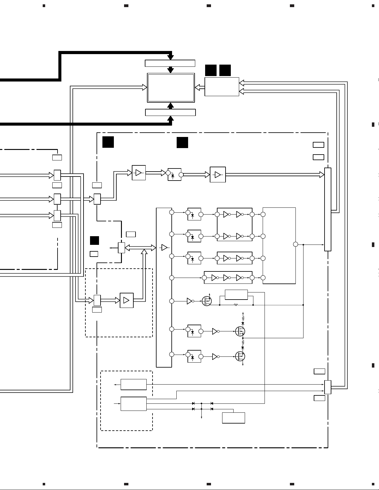
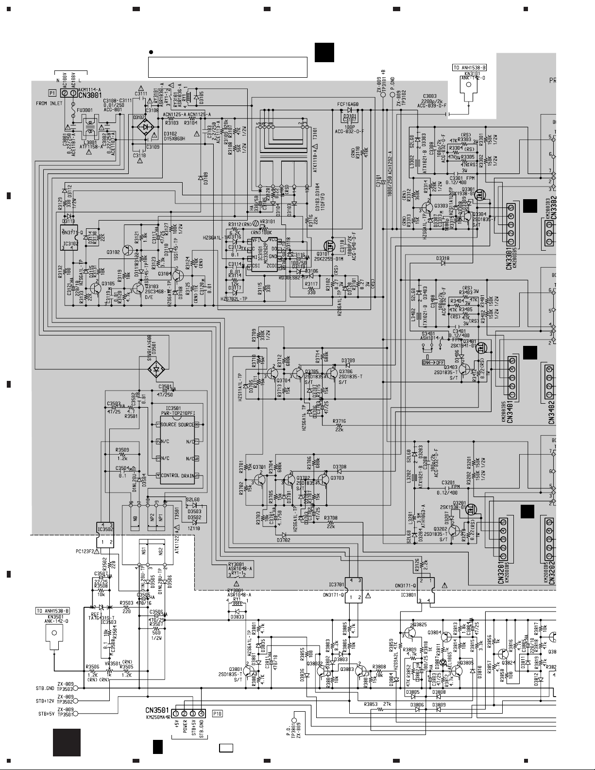
3.2 OVERALL WIRING DIAGRAM
4
AC INLET
AKP1211
A
CN5005
G
Y3
AC100–120V
50/60 Hz
LIVE
NEUTRAL
ADX2586
ADX2585
S1: POWER SW
BSM1010
ADX2584
E
CN4001
X10
E
ADX2607
CN4004
X2
ADX2607
OTL CONTROL (A) ASSY
U
N
(AWZ6177)
SUB POWER ASSY
(AWZ6173)
RCC CONTROL (A) ASSY
R
K
ADX2607
X3
CN4005
E
A
B
C
X1
F
X1
CN4003
CN4003
E
C 1/4- C 4/4
(AWZ6174)
ANALOG VIDEO ASSY
(AWQ1056)
B
B
CN7355CN7358
B 1/6- B 6/6
CN7251
CONTROL ASSY
(AWZ6545)
CN3204CN3202
CN3201
C
FAN RELAY ASSY
K
(AWZ6535)
IR RECEIVER
J
ASSY
(AWZ6526)
CN7850
CN7001
CN7354
3D Y/C ASSY
Q
(AWQ1055)
FAN MOTOR ×5
AXM1039
CN7650 CN7002 CN7000 CN7351
J81
ADX2614
INPUT CONTROL ASSY
(AWZ6554)
A
A
A 1/2- A 2/2
KM250MA8R
D
CN3203
C
22
ADX2650
1234
Page 23
5
678
PDP-V402
Note : When ordering service parts, be sure to refer to "EXPLODED VIEWS and PAR TS LIST" or "PCB PARTS LIST".
ADX2607
G
OTL CONTROL (B) ASSY
V
(AWZ6178)
RCC CONTROL (B) ASSY
S
(AWZ6175)
CN5004
Y2
ADX2607
G
CN5001
Y16
ADX2361
MAIN POWER ASSY
M
(AWR1077)
RCC CONTROL (C) ASSY
T
(AWZ6176)
ADX2652
H
ADX2646
Y1
CN5003
ADX2609
E
Y1
CN4008
X4
FAN MOTOR ×2
AXM1038
C
CN5008
H
A
Y5
B
ADX2630ADX2341
CN5003
G
B
ADX2607
CN7250
CN7003
ADX2608
CN7352
CN7501 CN7350
ADX2644
ADX2645
ADX2651
D.RESET
VGA60_75
ADX2649
D
D 1/10- D 10/10
DIGITAL VIDEO ASSY
(AWP1069)
J7800
G
and
H
CN5007
Y4
CN5007
Y4
C
D
CN7750 CN7800
L
B8B-PH-SM3
SYNC DET
ASSY
(AWZ6548)
5
FRONT KEY
I
ASSY
(AWZ6525)
ADX2639
ADX2632 ADX2633 ADX2633 ADX2634
ADX2635 ADX2636 ADX2638 ADX2638 ADX2637
6
7
To ADDRESS
MODULE
23
8
Page 24
1
PDP-V402
23
4
CN1602
N
SP2
A
M
CN3203
P6
M
CN3404
P4
M
CN3305
P3
D
CN6701
E11
D
CN6702
E12
D
CN6703
E13
E
X DRIVE (A) ASSY
(AWP1078)
E6
B
CN6551
D
PLASMA PANEL ASSY
(AAV1235)
C
F
X DRIVE (B) ASSY
(AWP1079)
D
M
CN3305
P3
24
CN6706
D
E16
1234
D
CN6707
E17
D
CN6708
E18
Page 25
5
678
PDP-V402
D
CN6704
E14
D
CN6705
E15
SCAN MODULE (B)
(AXF1105)
P
SCAN MODULE (B)
(AXF1105)
CN1602
N
SP2
M
G
Y DRIVE (A) ASSY
(AWZ6533)
P2
M
CN3405CN3304
P5
M
CN3204
P7
A
D
CN6553
E8
B
P
SCAN MODULE (A)
(AXF1104)
O
H
Y DRIVE (B) ASSY
(AWP1077)
CN6553
D
M
CN3304
C
E8
P2
D
5
CN6709
E19
D
CN6710
E20
SCAN MODULE (A)
(AXF1104)
O
6
CN6552
D
E7
25
7
8
D
Page 26
1
PDP-V402
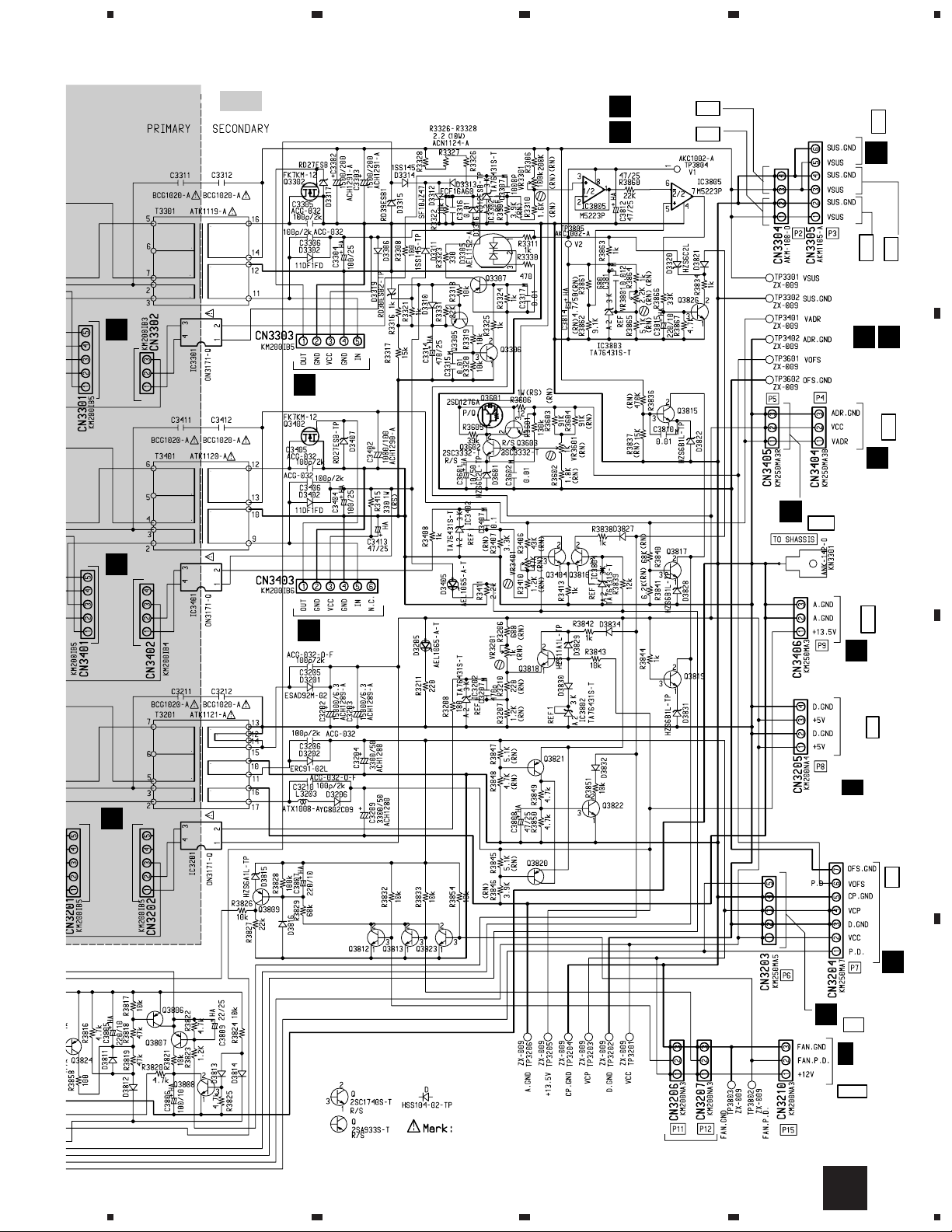
3.30 MAIN POWER ASSY
To POWER SWITCH
A
23
NOTE FOR FUSE REPLACEMENT
CAUTION: FOR CONTONUED PROTECTION AGAINST RISK OF FIRE.
PEPLACE ONLY WITH SAME TYPE AND RATINGS ONLY.
J
M
4
MAIN POWER ASSY (AWR1077)
R
CN7101
CN7102
B
C
S
CN7151
CN7152
T
CN7201
CN7202
D
78
M
B 1/6
CN7005
M2
1234
Page 27
5
678
PDP-V402
7)
R
CN7101
CN7102
1000P
/AC400
1000P
/AC400
: Charged section
1000P
/AC400
CN7251
1000P
/AC400
U
H
CN5003
G
CN5003
Y1
Y1
CN5001
G
Y16
X1
E
CN4003
X1
SP1
CN1601
CN4003
F
N
X10
CN4001
E
A
B
S
CN7151
CN7152
T
CN7201
CN7202
1000P
/AC400
1000P
/AC400
V
CN7301
SP4
CN1604
N
E1
CN6102
C
D 1/10
Y2
CN5004
G
CN4004
E
X2
Be sure to use parts od identical designation.
B 6/6
CN7900
M20
D
To FAN
M
5
6
7
8
79
Page 28
1
PDP-V402
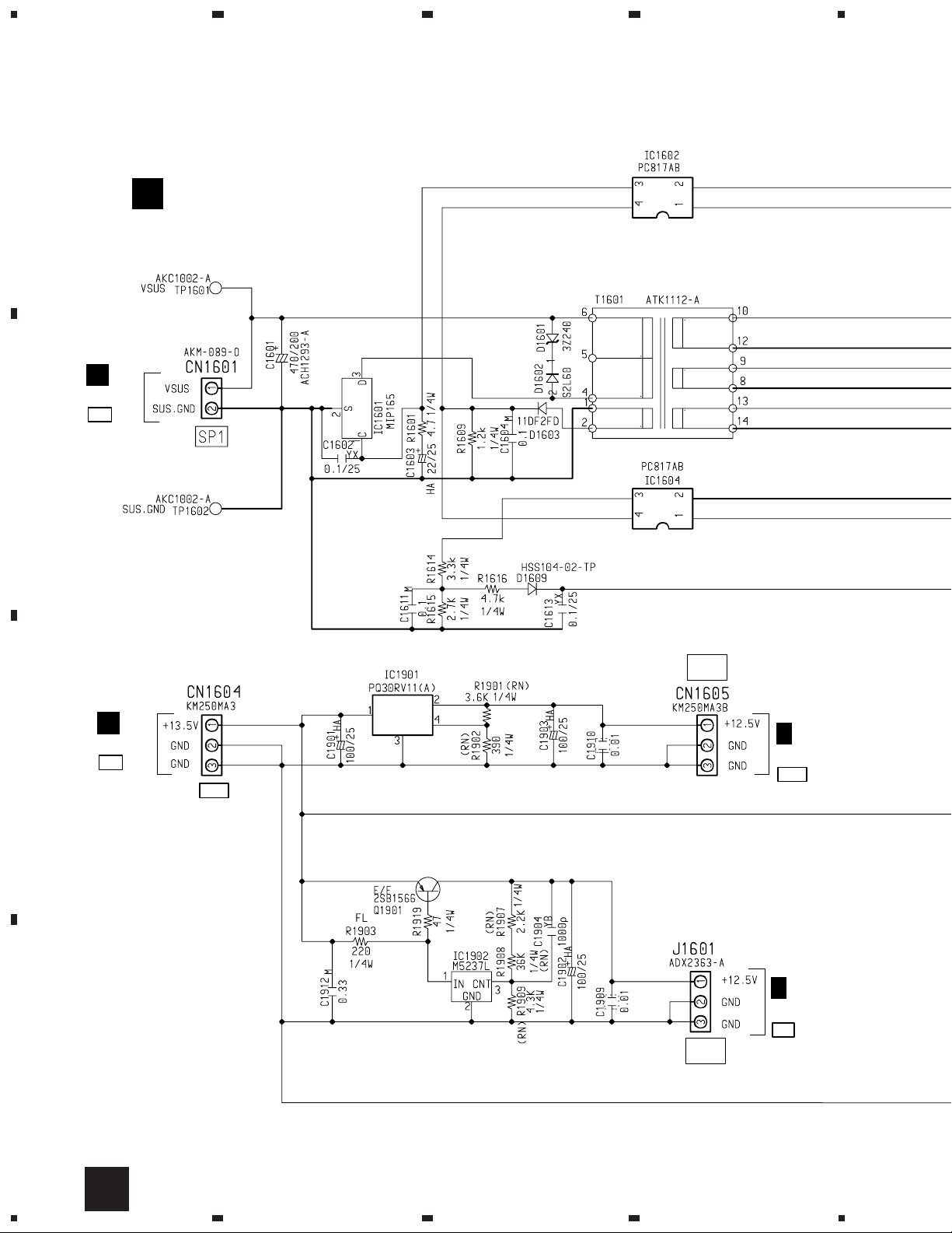
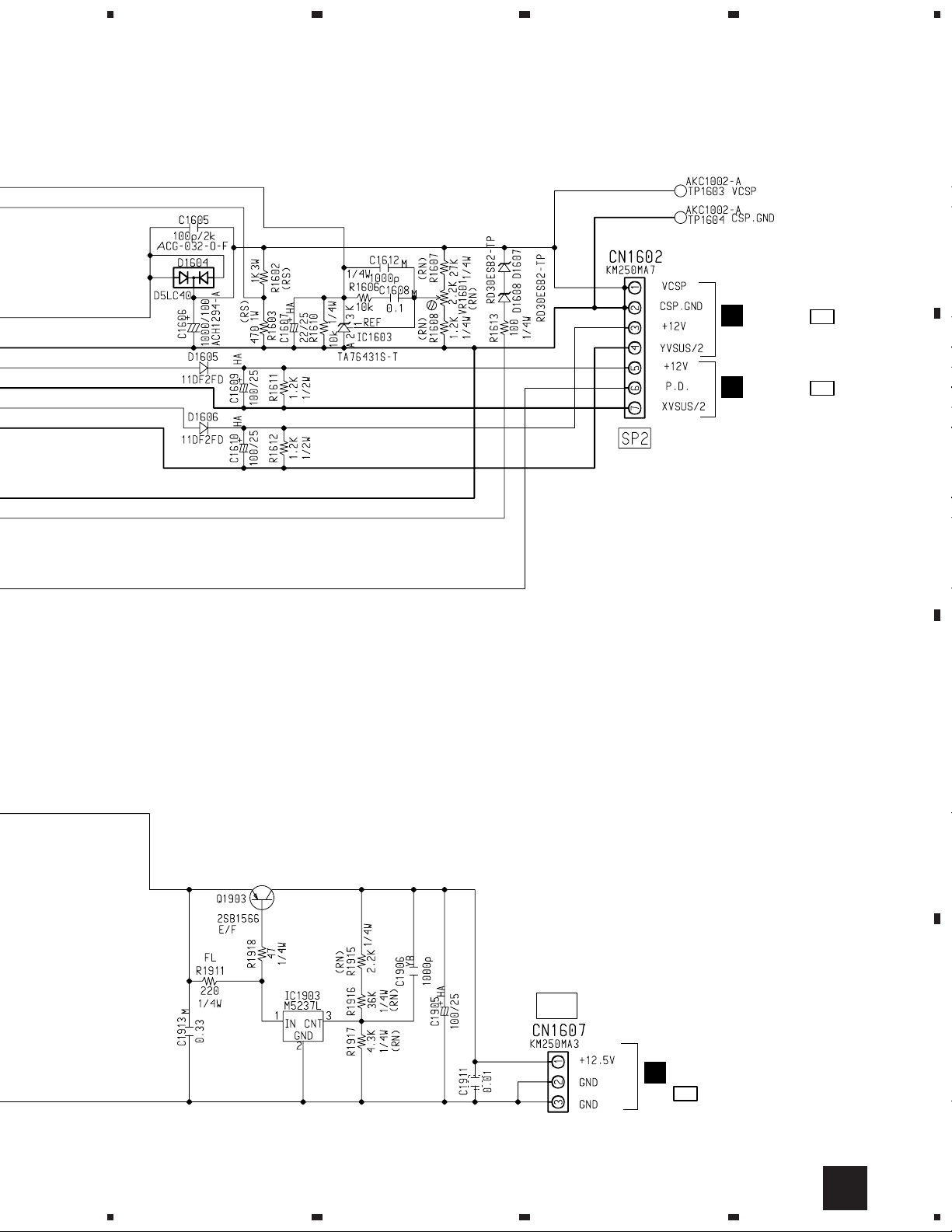
3.31 SUB POWER SUPPLY
A
SUB POWER ASSY
N
(AWZ6173)
M
CN3305
P3
B
23
4
SP3
M
CN3406
C
P9
SP4
B 5/6
CN7650
M14
C 2/4
CN2204
A4
SP5
D
80
N
1234
Page 29
5
678
PDP-V402
A
G
E
CN5005
CN4005
Y3
X3
B
C
SP6
Q
CN3202
B1
N
5
6
7
8
81
D
Page 30
1
Y
L
23
PDP-V402
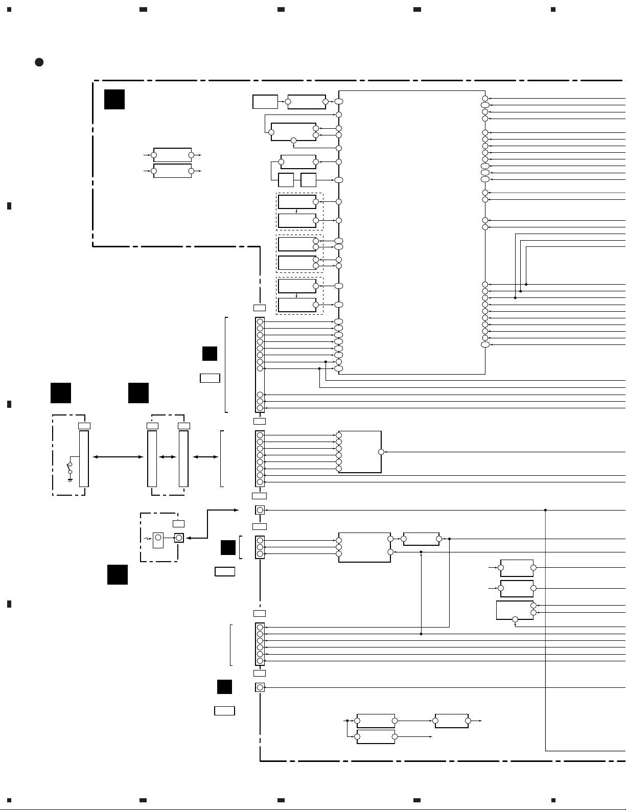
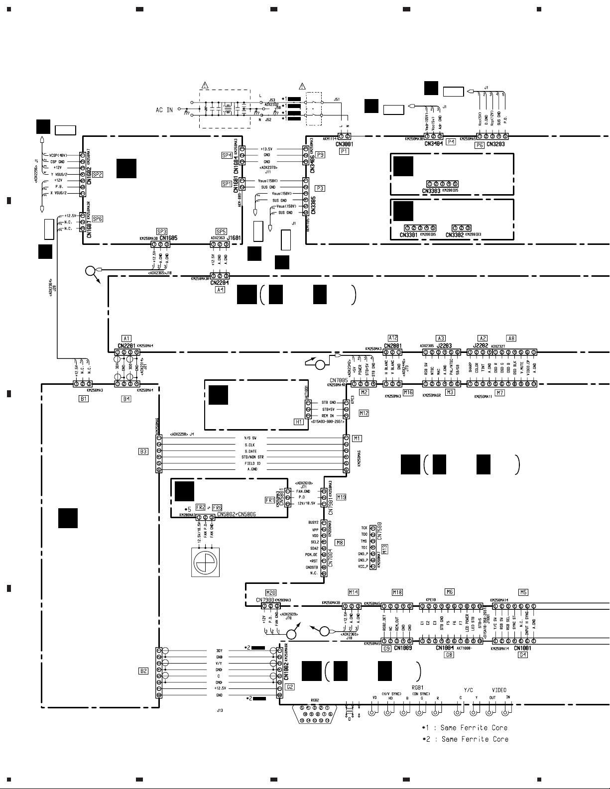
4. PCB CONNECTION DIAGRAM
NOTE FOR PCB DIAGRAMS:
1. Part numbers in PCB diagrams match those in the schematic
A
diagrams.
2. A comparison between the main parts of PCB and schematic
diagrams is shown below.
Symbol in PCB
Diagrams
BCE
BCE
DGS
Symbol in Schematic
Diagrams
BCE
BCE
BCEBCE
DGSDGS
Part Name
Transistor
Transistor
with resistor
Field effect
transistor
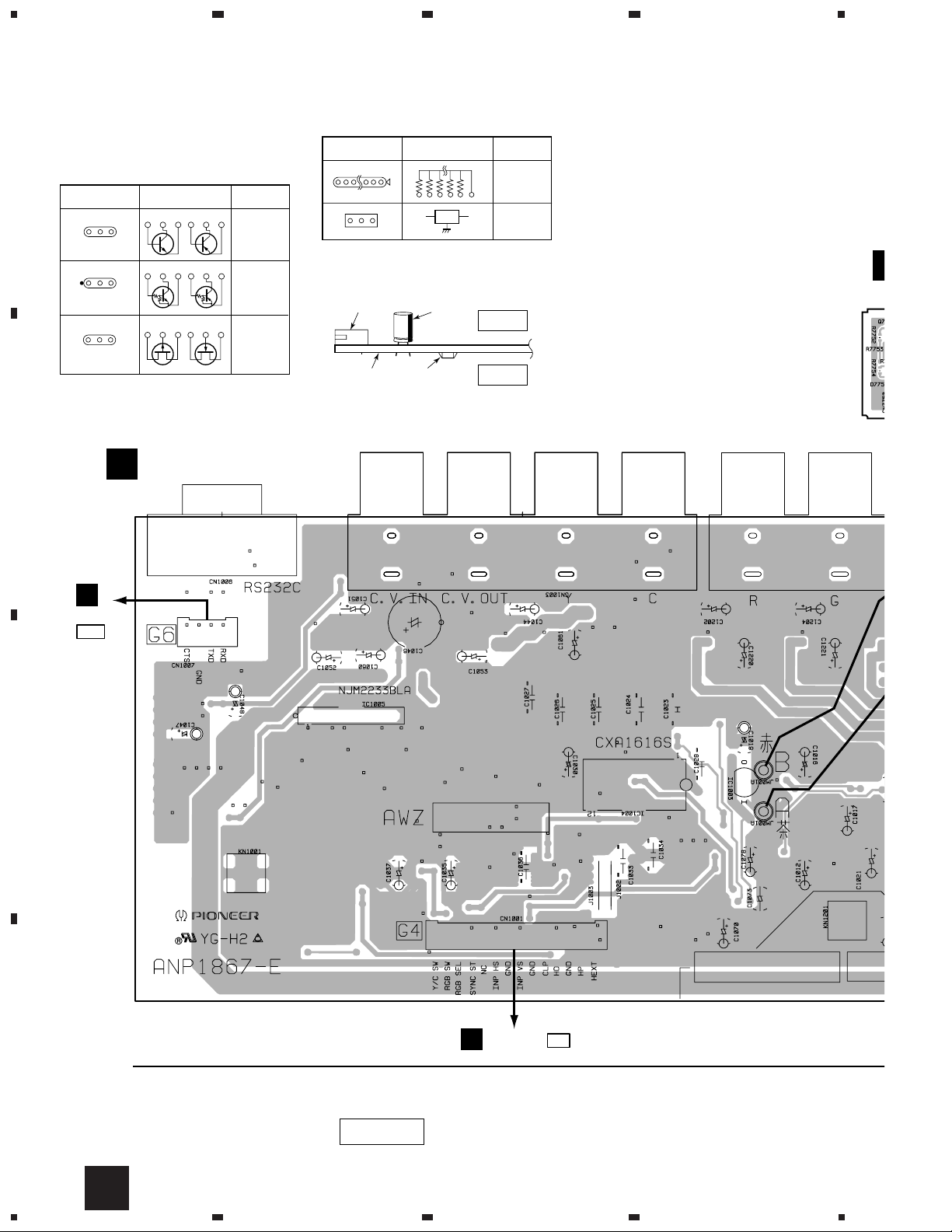
4.1 INPUT CONTROL, FRONT KEY, SYNC DET ASSYS
Symbol in PCB
Diagrams
3. The parts mounted on this PCB include all necessary parts
for several destination.
For further information for respective destinations, be sure
to check with the schematic diagram.
4. Viewpoint of PCB diagrams
P. C. Board Chip Part
Symbol in Schematic
Diagrams
CapacitorConnector
Part Name
Resistor array
3-terminal
regulator
SIDE A
SIDE B
4
S
B
INPUT CONTROL ASSY
A
B
CN7003
M11
C
CN7351
B
D
IC1005 IC1004 IC1003
M5
SIDE A
90
A
1234
Page 31

5
678
PDP-V402
FRONT KEY ASSY
I
A
L
SYNC DET ASSY
(ANP1968-C)
(ANP1968-C)
B
B
CN7000
M6
(ANP1867-E)
CN7002
B
5
6
M18
IC1006
CN3203
Q
B2
CN2401
C
7
A5
LIA
8
91
C
D
Page 32

PDP-V402
Q
A
1
FRONT KEY ASSY
I
23
(ANP1968-C)
L
SYNC DET ASSY
4
B
INPUT CONTROL ASSY
A
C
(ANP1968-C)
Q1204 Q1206 Q1038 Q1039 Q1041
D
Q1208 Q1207
Q1205
Q1025 Q1024
Q1040 Q1203
Q1001 – Q1007IC1001Q1046IC1201 Q1037Q1036Q1209
Q1048
Q1008
SIDE B
92
1234
LIA
Page 33

5
678
PDP-V402
A
)
B
C
Q1203 Q1202 Q1201 Q1027 Q1028 Q1026 Q1034
7 IC1002
Q1008
048
Q1045 Q1044
5
Q1042 Q1043 Q1010
Q1015Q1047 Q1014Q1013 Q1016 Q1017
Q1019Q1020 Q1018
6
Q1022
(ANP1867-E)
Q1035Q1012Q1021Q1009
7
Q1029 – Q1032
Q1033
A
8
D
93
Page 34

1
Q
PDP-V402
23
4
4.2 CONTROL ASSY
A
B
IC7654
Q7653
Q7657
Q7650
Q7656
Q7854
IC7650
Q7260 Q7257
Q7254 Q7255
Q7259 Q7258
Q7253 Q7256
Q7259 Q7258
Q7253 Q7256
Q7659
IC7252
IC7653
IC7652IC7352
IC7254
IC7350
N
CN1605
SP3
VR7650
D
CN6103
E2
CONTROL ASSY
B
D
IC7500
IC7006
IC7506
Q7359
Q7360
Q7015
Q7016
CN6603
E21
D
CN6104
E3
IC7351
IC7502
C
IC7501
IC7505
IC7507
Q7364
Q7350–Q7353
Q7361 Q7366
D
94
SIDE A
CN1001
A
G4
C
J2203
A3
CN7850
J
H1
B
1234
Page 35

5
678
PDP-V402
C
J2601
A6
C
J2202
A8A2
A
Q7251
IC7901
Q7250
IC7902
Q7261 Q7269
IC7903
Q7268
Q7905
Q7906
Q7900
Q7904
Q7014
Q7368
Q7367
Q7365
Q7362
Q7909
B
M
CN3120
P15
Q7266
Q7252
IC7253
IC7900
Q7907
Q7908
Q7008
Q7012
K
CN5801
FR1
C
CN2801
A12
A
CN1009
G9
A
CN1007
G6
IC7254
IC7002
IC7503
IC7504
Q7019
IC7005
Q7020
IC7001
Q7001
Q7000
IC7000
Q7017
Q7021
Q7002
Q7007
C
IC7003
H1 B3
Q
CN3201
5
M
CN3501
P10
CN1004
A
6
G8
(ANP1968-C)
7
Q7013
Q7018
B
8
D
95
Page 36

PDP-V402
A
B
1
23
CONTROL ASSY
B
4
C
D
SIDE B
96
B
1234
Page 37

5
678
PDP-V402
A
B
C
D
(ANP1968-C)
B
5
6
7
8
97
Page 38

1
C
PDP-V402
4.3 ANALOG VIDEO ASSY
23
4
CN7251
B
A
B
ANALOG VIDEO ASSY
C
M7
B
Q
CN3204
B4
C
D
98
SIDE A
CN7358
B
M16
C
1234
CN1201
A
G1
Page 39

5
678
PDP-V402
B
CN7355
M3
CN7251
B
M7
CN7250
B
M4
CN6101
D
E5
N
J1601
SP5
VR2201
Q2651
Q2652
Q2653
IC2802
IC2601
IC2201
A
B
(ANP1894-C)
VR2802
VR2803
VR2801
IC2801
C
D
C
5
6
7
8
99
Page 40

PDP-V402
Q
9
2
A
B
1
ANALOG VIDEO ASSY
C
23
4
C
D
Q2615 Q2616 Q2611 Q2614 Q2607 Q2610 IC2602
Q2631 Q2650 Q2627 Q2649 Q2629 Q2648
SIDE B
100
C
1234
Q2635 Q2633 Q2634Q2603 Q2604
Q2608Q2612Q2618
Q2637Q2609Q2613Q2617
IC2402
Q2601Q2602 Q2605 Q2606
Q2636
Q2646Q2626
Q2642 Q2621 Q2630Q2641
Q2416 Q2415 Q2408 Q2413 Q2407 Q2412 Q2409 Q2414
Q2644
Q2620
Q2638
Q2619
Q2632Q2411
Q2640Q2645
Q2639
Q2647
Q2625Q2624 Q2628Q2623
Q2417 Q2405 Q2403
IC2603
Q2431
Q2428
Q2433
Q221
Q2404
Q2437
Q2406
Q2410
Q
Page 41

5
4
678
PDP-V402
A
B
C
(ANP1894-C)
Q2431
Q2428
Q2433
Q2219 Q2228
Q2404
Q2437
Q2406
Q2410
14
Q2213 Q2212 Q2211 Q2210 Q2806 Q2820 Q2814 Q2216
Q2223
Q2424 Q2421
Q2423 Q2422 Q2425 IC2401
Q2227 Q2208 Q2209 Q2228
Q2224 Q2206 Q2207 Q2225
Q2420 Q2419 Q2426 Q2418
5
6
Q2203 Q2204 Q2202
Q2804 Q2810 Q2809
Q2807 Q2819Q2817
7
Q2813
Q2812
Q2811Q2205Q2215Q2214
Q2801Q2802Q2803Q2201
Q2816 Q2816 Q2815
Q2808
C
8
101
D
Page 42

1
PDP-V402
4.4 DIGITAL VIDEO ASSY
DIGITAL VIDEO ASSY
D
A
IC6102
IC6101
Q6101
IC6206
IC6105
Q6102
IC6604
IC6106
Q6103
B
C
CN2602
A7
23
M
CN3205
P8
4
IC6201
IC6103
B
IC6104
CN7352
M9
IC6601
B
CN7350
IC6603
C
IC6001
Q6002
IC6005
Q6001
IC6006
IC6002
IC6007
IC6008
IC6003
IC6004
IC6503
IC6305
Q6004
M17
B
CN7501
M10
E21
Q6003
IC6602
D
SIDE A
102
D
1234
Page 43

5
ADDRESS MODULE (B)
678
PDP-V402
A
E
CN4008
X4
H
CN5008
Y5
G
CN5007
Y4
and
H
CN5007
Y4
IC6705
IC6708
IC6308
IC6405
IC6502
IC6553
IC6401
IC6402
IC6301
IC6552
IC6403
IC6404
IC6556
IC6501
IC6551
B
C
ADDRESS MODULE (A)
5
IC6305
IC6554
IC6555
IC6701
VR6551
IC6704
VR6554
D
(ANP1866-D)
D
6
7
103
8
Page 44

PDP-V402
A
B
1
DIGITAL VIDEO ASSY
D
23
4
C
D
SIDE B
104
D
1234
Page 45

5
678
PDP-V402
A
Q6105
Q6104
Q6106
Q6107
B
C
D
(ANP1866-D)
D
5
6
7
105
8
Page 46

1
PDP-V402
4.5 X DRIVE (A) ASSY
23
4
A
B
CN3305
M
P3
ADDRESS
MODULE
(B)
X DRIVE (A) ASSY
E
PLASM PANEL ASSY
CN4010
F
X6
CN3404
C
D
M
D
P4
CN6551
E6
IC4003
IC4015 IC4022
IC4002 IC4001
IC4014IC4008 IC4013 IC4012 IC4009
F
IC4005
CN4009
X9
IC4007
IC400
SIDE A
106
E
1234
Page 47

5
678
PDP-V402
A
CN1602
N
SP2
B
F
F
CN4006
X8
CN4019
X7
C
4007
VR4002
IC4017 Q4011
5
CN4011
F
Q4012 Q4013 Q4014IC4021 IC4024
X5
M
IC4019 IC4023
IC4028IC4004IC4011IC4006
Q4003
Q4004IC4010 Q4007 Q4005
6
CN3203
P6
Q4001
Q4002
Q4006IC4020
7
(ANP1970-B)
Q4008
E
8
D
107
Page 48

PDP-V402
A
B
1
X DRIVE (A) ASSY
E
23
4
C
D
SIDE B
108
E
1234
Page 49

5
678
PDP-V402
A
B
C
(ANP1970-B)
D
109
E
5
6
7
8
Page 50

1
PDP-V402
4.6 X DRIVE (B) ASSY
23
4
A
B
M
CN3305
P3
ADDRESS
MODULE
(A)
X DRIVE (B) ASSY
F
PLASM PANEL ASSY
CN4010
E
X6
C
CN4009
E
IC4003
IC4015 IC4022
D
IC4002 IC4001
IC4014IC4008 IC4013 IC4012 IC4009
IC4005
X9
IC4007
IC400
SIDE A
110
F
1234
Page 51

5
678
PDP-V402
A
B
E
E
CN4006
X8
CN4019
X7
C
4007
VR4002
IC4017 Q4011
5
CN4011
E
Q4012 Q4013 Q4014IC4021 IC4024
X5
IC4019 IC4023
IC4028IC4004IC4011IC4006
Q4003
Q4004IC4010 Q4007 Q4005
6
Q4001
Q4002
Q4006IC4020
7
(ANP1970-B)
Q4008
F
8
D
111
Page 52

PDP-V402
A
B
1
X DRIVE (B) ASSY
F
23
4
C
D
SIDE B
112
F
1234
Page 53

5
678
PDP-V402
A
B
C
(ANP1970-B)
D
113
F
5
6
7
8
Page 54

1
5
PDP-V402
4.7 Y DRIVE (A) ASSY
A
M
CN3304
P2
23
Y DRIVE (A) ASSY
G
4
CN1
P
P
D
CN2
CN1
CN2
CN6553
E8
B
C
Y14
Y13
Y12
Y11
Y14
Y11 Y13Y12
D
IC5003
IC5022 IC5015 IC5023 IC5024
SIDE A
114
G
1234
CN5014
H
Y6
IC5002 IC5001 IC5011 IC5019
IC5008 IC5010 IC5009
CN3405
M
P5
IC5014 IC5025 IC5005 IC5013
H
CN5009
Y9
VR5003
ADDRESS
MODULE(B)
CN5018
H
IC5030IC5029IC5028IC5027
Y7
IC5031 IC5032
IC
IC5006
Page 55

5
678
PDP-V402
A
B
Y13
H
CN5015
Y10
H
CN5006
Y8
N
CN1602
SP2
C
5032
IC5004
IC5018 IC5039
IC5006
VR5002
5
Q5006
Q5007 Q5012
Q5001 Q5002
Q5010 Q5011
(ANP1971-B)
CN3204
M
P7
Q5008 Q5009IC5020 IC5033
IC5034
IC5017 IC5007 IC5038
Q5003
6
7
IC5018
IC5035 IC5021IC5026
G
115
8
D
Page 56

PDP-V402
A
B
1
Y DRIVE (A) ASSY
G
23
4
C
D
SIDE B
116
G
1234
Page 57

5
678
PDP-V402
A
B
C
(ANP1971-B)
G
5
6
7
117
8
D
Page 58

1
5
PDP-V402
23
4
4.8 Y DRIVE (B) ASSY
A
M
CN3304
P2
CN1
O
O
CN2
CN1
CN2
B
Y14
Y13
Y12
Y11
Y DRIVE (B) ASSY
H
Y14
CN6552
D
D
E7
CN6553
E8
C
Y11 Y13Y12
D
IC5003
IC5022 IC5015 IC5023 IC5024
SIDE A
118
H
1234
CN5014
G
Y6
IC5002 IC5001 IC5011 IC5019
IC5008 IC5010 IC5009
IC5014 IC5025 IC5005 IC5013
G
CN5009
Y9
VR5003
ADDRESS
MODULE(A)
CN5018
G
IC5030IC5029IC5028IC5027
Y7
IC5031 IC5032
IC
IC5006
Page 59

5
678
PDP-V402
A
B
Y13
G
CN5015
Y10
G
CN5006
Y8
C
5032
IC5004
IC5018 IC5039
IC5006
VR5002
5
Q5006
Q5007 Q5012
Q5001 Q5002
Q5010 Q5011
6
Q5008 Q5009IC5020 IC5033
IC5034
IC5017 IC5007 IC5038
Q5003
(ANP1971-B)
IC5035 IC5021IC5026
IC5018
H
7
119
8
D
Page 60

PDP-V402
A
B
1
Y DRIVE (B) ASSY
H
23
4
C
D
SIDE B
120
H
1234
Page 61

5
678
PDP-V402
A
B
C
(ANP1971-B)
H
5
6
7
121
8
D
Page 62

1
PDP-V402
4.9 MAIN POWER ASSY
MAIN POWER ASSY
M
A
23
E
F
CN4003
CN4003
X1
X1
CN1601
N
SP1
G
CN5001
Y16
H
CN5003
Y1
4
G
CN5003
Y1
E
CN40
X10
B
U
CN7251
V
CN7301
R
CN7101
C
R
CN7102
S
CN7151
S
CN7152
T
CN7201
T
CN7202
D
SIDE A
122
M
1234
Page 63

5
678
PDP-V402
003
E
CN4001
X10
N
CN1604
SP4
D
CN6102
E1
E
CN4004
X2
G
CN5004
Y2
FAN
MOTOR
B
CN7900
M20
B
CN7005
M2
VR3201
VR3601
VR3301
VR3401
VR3501
Q3819
Q3820
Q3307
Q3826
IC3302
IC3803
Q3404
Q3305
IC3805
Q3306
Q3302
Q3402
Q3823
Q3818
IC3802
IC3202
Q3821
Q3822
Q3817
Q3815
IC3804
Q3816
Q3805
Q3206
Q3201
Q3802
Q3801
Q3803
Q3813
Q3601
Q3812
Q3811
Q3603
Q3810
Q3602
Q3809
Q3806
Q3807
Q3808
Q3804
Q3824
A
B
VR3101
Q3825
IC3801 IC3503
IC3701
IC3301
IC3201
Q3704
Q3705
Q3706
IC3501
Q3701
Q3702
Q3703
Q3202
Q3201
Q3301
Q3101
Q3401
Q3303
Q3304
Q3104
IC3102
IC3101
Q3105
Q3102
Q3103
C
D
(ANP1864-D)
5
6
7
S1: POWER SW
M
8
123
Page 64

PDP-V402
A
B
1
M
23
MAIN POWER ASSY
4
C
D
SIDE B
124
M
1234
Page 65

5
678
PDP-V402
A
B
C
D
(ANP1864-D)
M
5
6
7
125
8
Page 66

1
R
23
PDP-V402
4.10 SUB POWER, RCC CONTROL (A), (B), (C),
OTL CONTROL (A), (B) ASSYS
4
CN3202
A
B
Q
B1
C
CN2204
A4
M
CN3406
P9
B
CN7650
M14
M
CN3305
P3
Q1904 Q1901 Q1902IC1903
C
RCC CONTROL (C) ASSY
T
IC1902 IC1901
RCC CONTROL (B) ASSY
S
(ANP1867-E)
CN3201
M
D
Q7201 Q7151IC7201 IC7151
M
CN3202
M
CN3401
M
(ANP1867-E)
CN3402
126
SIDE A
N
S T
1234
Page 67

5
SUB POWER ASSY
N
678
PDP-V402
A
B
(ANP1867-E)
CN5005
G
IC1601 IC1602 IC1603
RCC CONTROL (A) ASSY
R
)
IC1604
(ANP1867-E)
Y3
OTL CONTROL
U
(A) ASSY
CN4005
E
(ANP1867-E)
X3
VR1601
OTL CONTROL
V
(B) ASSY
C
(ANP1867-E)
CN3301
M
Q7101 IC7101 Q7253
5
M
CN3302
CN3303
M
Q7252
IC7251
6
Q7251
7
N
CN3403
M
Q7303
Q7302
IC7301
Q7301
R U V
8
D
127
Page 68

1
S
PDP-V402
23
4
A
B
SUB POWER ASSY
N
OTL CONTROL
C
V
(B) ASSY
OTL CONTROL
U
(A) ASSY
RCC CONTROL (A) ASSY
R
(ANP1867-E)(ANP1867-E)(ANP1867-E)
D
SIDE B
128
N
R U V
1234
Page 69

5
678
PDP-V402
A
B
67-E)
RCC CONTROL (B) ASSY
S
RCC CONTROL (C) ASSY
T
(ANP1867-E)
C
(ANP1867-E)(ANP1867-E)
D
N
5
6
7
S T
129
8
Page 70

1
PDP-V402
4.11 3D Y/C ASSY
3D Y/C ASSY
Q
A
B
23
4
Q3220
Q3208
|
Q3223
Q3222
Q3214
|
Q3218
Q3224
Q3201
IC3203
Q3225
Q3203
Q3204
Q3205
Q3212
IC3205
Q3206
Q3210
C
IC3204
IC3202
IC3206
IC3201
D
C
CN2201
A1
N
CN1607
SP6
CN7354
B
M1
CN1002
A
G2
(ANP1974-A)
SIDE A
130
Q
1234
Page 71

1
3D Y/C ASSY
Q
234
PDP-V402
A
B
C
D
(ANP1974-A)
SIDE B
Q
1
2
3
131
4
Page 72

1
23
PDP-V402
4.12 IR RECEIVER, FAN RELAY ASSYS
A
J
IR RECEIVER ASSY
B
CN7001
M12
(ANP1968-C)
B
CN7901
M19
FAN RELAY ASSY
K
4
B
(ANP1971-B)
SIDE A
FAN MOTOR
SIDE B
C
J
IR RECEIVER ASSY
FAN RELAY ASSY
K
(ANP1968-C)
(ANP1971-B)
D
132
J
K
1234
Page 73

5. PCB PARTS LIST
NOTES:•Parts marked by "NSP" are generally unavailable because they are not in our Master Spare Parts List.
The mark found on some component parts indicates the importance of the safety factor of the part.
•
Therefore, when replacing, be sure to use parts of identical designation.
When ordering resistors, first convert resistance values into code form as shown in the following examples.
•
Ex.1 When there are 2 effective digits (any digit apart from 0), such as 560 ohm and 47k ohm (tolerance is shown by J=5%,
and K=10%).
560 Ω→56 × 10
47k Ω→47 × 10
1
→ 561 ........................................................ RD1/4PU 5 6 1 J
3
→ 473 ........................................................ RD1/4PU 4 7 3 J
0.5 Ω→R50 ..................................................................................... RN2H R 5 0 K
Ex.2 When there are 3 effective digits (such as in high precision metal film resistors).
5.62k Ω→ 562 × 10
1
→ 5621 ...................................................... RN1/4PC 5 6 2 1 F
1 Ω→1R0 ..................................................................................... RS1P
1 R 0
PDP-V402
K
Mark No. Description Part No.
LIST OF ASSEMBLIES
NSP COMPLEX (A) ASSY AWV1875
INPUT CONTROL ASSY AWZ6554
SUB POWER ASSY AWZ6173
RCC CONTROL (A) ASSY AWZ6174
RCC CONTROL (B) ASSY AWZ6175
RCC CONTROL (C) ASSY AWZ6176
OTL CONTROL (A) ASSY AWZ6177
OTL CONTROL (B) ASSY AWZ6178
NSP COMPLEX (B) ASSY AWV1861
CONTROL ASSY AWZ6545
FRONT KEY ASSY AWZ6525
IR RECEIVER ASSY AWZ6526
SYNC DET ASSY AWZ6548
3D Y/C ASSY AWQ1055
ANALOG VIDEO ASSY AWQ1056
DIGITAL VIDEO ASSY AWP1069
X DRIVE (A) ASSY AWP1078
X DRIVE (B) ASSY AWP1079
Y DRIVE (B) ASSY AWP1077
MAIN POWER ASSY AWR1077
NSP Y DRIVE (A)/SENSOR ASSY AWV1854
Y DRIVE (A) ASSY AWZ6533
FAN RELAY ASSY AWZ6535
SCAN MODULE (A) AXF1104
SCAN MODULE (B) AXF1105
Mark No. Description Part No.
D1001-D1004,D1006,D1007 1SS226
D1009-D1012,D1016,D1017 1SS226
D1201-D1206 1SS226
D1005,D1008,D1013-D1015,D1207 RD15MB
COILS
L1001 ATH1046
L1002 ATX1008
SWITCHES
S1001 ASH1029
S1201,S1202 ASH1046
CAPACITORS
C1004,C1006 CCSQCH470J50
C1014 CEANP100M35
C1009 CEANP100M50
C1001-C1003,C1005,C1013 CEANP101M10
C1040,C1073 CEANP1R0M50
C1010 CEANPR22M50
C1044,C1051-C1053,C1056,C1202 CEAS101M10
C1204,C1206,C1208,C1210,C1212 CEAS101M10
C1007,C1017,C1019,C1021,C1030 CEAS101M25
C1037,C1048,C1058,C1060-C1062 CEAS101M25
C1064,C1214,C1219-C1221 CEAS101M25
C1054 CEAS102M16
C1046 CEAS102M6R3
C1078 CEAS1R0M50
C1011,C1012,C1015,C1016,C1035 CEAS470M25
INPUT CONTROL ASSY
A
SEMICONDUCTORS
IC1004 CXA1616S
IC1005,IC1006 NJM2233BLA
IC1002 NJM319M
IC1003 NJM78L05A
IC1001,IC1201 TC4053BF
Q1001,Q1004,Q1005,Q1008,Q1009 2SA1162
Q1011-Q1018,Q1024-Q1026 2SA1162
Q1030,Q1031,Q1033,Q1042,Q1043 2SA1162
Q1207-Q1209 2SA1162
Q1002,Q1003,Q1006,Q1007,Q1010 2SC2712
Q1019-Q1022,Q1027-Q1029,Q1032 2SC2712
Q1034-Q1041,Q1044,Q1045 2SC2712
Q1047,Q1048,Q1201-Q1206 2SC2712
C1047,C1070,C1072 CEAS470M25
C1025,C1028 CFTLA104J50
C1033 CFTLA223J50
C1023,C1026 CFTLA224J50
C1024 CFTLA684J50
C1032 CKSQYB102K50
C1008,C1018,C1020,C1022,C1031 CKSQYB103K50
C1038,C1042,C1043,C1045 CKSQYB103K50
C1049,C1050,C1055,C1059,C1063 CKSQYB103K50
C1065,C1066,C1071,C1201,C1203 CKSQYB103K50
C1205,C1207,C1209,C1211,C1213 CKSQYB103K50
C1215,C1216,C1225-C1230 CKSQYB103K50
C1079 CKSQYB221K50
C1067-C1069,C1222-C1224 CKSQYF104Z50
C1036 CQMA164J50
C1027 CQMA182J50
C1034 CQMA562J50
133
Page 74

PDP-V402
Mark No. Description Part No.
RESISTORS
R1254-R1256 RD1/4PU751J
R1023 RD1/4PU753J
R1021,R1029 RS1/10S1002F
R1022 RS1/10S1102F
R1030 RS1/10S1202F
R1025,R1033 RS1/10S2701F
R1026,R1034 RS1/10S3901F
R1117 RS2MMF2R2J
Other Resistors RS1/10S J
OTHERS
J1004 8P BOARD IN WIRE ADX2549
CN1006 9P D-SUB SOCKET AKP1171
CN1203 15P D-SUB SOCKET AKP1172
CN1202 BNC SOCKET AKX1050
CN1003 BNC SOCKET AKX1053
KN1001,KN1201
J1001 JUMPER WIRE D15A10-350-2651
CN1001 PLUG 14-P KM250MA14
CN1007 PLUG 4-P KM250MA4B
CN1009 PLUG 5-P KM250MA5
CN1201 PLUG 6-P KM250MA6
CN1002 PLUG 8-P KM250MA8R
CN1005 CONNECTOR 10P KPE10
SCREW TERMINAL
ANG2256
Mark No. Description Part No.
Q7002-Q7004,Q7359,Q7360,Q7362 DTA124EK
Q7365,Q7900,Q7901 DTA124EK
Q7021,Q7350-Q7352,Q7361,Q7364 DTC124EK
Q7366-Q7368,Q7904,Q7908 DTC124EK
Q7005-Q7007 DTC143EK
D7012,D7013,D7021-D7023 1SS226
D7500-D7502,D7504-D7507 1SS226
D7001,D7002,D7005-D7007,D7009 1SS355
D7250-D7261,D7503,D7656 1SS355
D7650-D7654 1SV228
D7014-D7018,D7020 UDZ15B
D7000 UDZ3.0B
D7008,D7019 UDZS6.8B
TH7900,TH7901 NTH4G42B104F01
COILS AND FILTERS
L7650 ATA9001
F7500,F7501,F7650-F7654 ATF1194
L7000 ATX1008
L7001 LCTA100J2520
L7250,L7251 LCTA2R2J2520
CAPACITORS
C7650 (1µ/20V) ACH1302
C7660 CCSQCH102J50
C7669 CCSRCH120J50
C7670 CCSRCH151J50
C7662 CCSRCH181J50
CONTROL ASSY
B
SEMICONDUCTORS
IC7001 24LC64(I)SN
IC7002 M38869FFAHP
IC7502
IC7902,IC7903 M5233FP
IC7252 M62358FP
IC7003 MC145407F
IC7251 NJM78L05UA
IC7250 NJM78L09UA
IC7000 PD5136
IC7253 PD5385A
IC7900,IC7901 PQ20VZ1U
IC7500 PQ3DZ13
IC7005,IC7006 PST9146N
IC7653 TC74ACT04FT
IC7503,IC7504,IC7652 TC74HC4538AFT
IC7350-IC7352,IC7505 TC74VHC541FT
IC7254 TC74VHCT541AFT
IC7004 TC7S66FU
IC7506,IC7651 TC7WU04FU
IC7501 TD74BC541F
IC7650 UPC1379C
IC7654 UPC78L05T
Q7659 2SA1037K
Q7010,Q7012,Q7013,Q7250-Q7260 2SA1162
Q7262,Q7264,Q7266,Q7269 2SA1162
Q7652,Q7653,Q7656-Q7658 2SC2412K
Q7000,Q7008,Q7009,Q7011 2SC2712
Q7014-Q7018,Q7020,Q7261,Q7263 2SC2712
Q7265,Q7268,Q7353,Q7902,Q7903 2SC2712
Q7905-Q7907,Q7909 2SC2712
Q7001 2SJ461
Q7654 2SK208
EPM7256AETC144-10
C7011,C7012,C7015,C7023,C7037 CCSRCH220J50
C7042,C7655 CCSRCH220J50
C7002,C7003 CCSRCH221J50
C7521,C7523,C7525,C7526,C7665 CCSRCH471J50
C7681,C7682 CCSRCH471J50
C7352,C7353 CCSRCH560J50
C7014,C7018 CCSRSL271J50
C7684 CEAT221M16
C7900-C7902 CEHV470M16
C7271,C7274,C7299,C7652,C7657 CEV100M16
C7685 CEV100M16
C7033,C7034,C7038,C7039 CEV100M35
C7674 CEV101M16
C7009,C7019,C7021,C7026,C7027 CEV101M6R3
C7035,C7045,C7046,C7259,C7350 CEV101M6R3
C7503,C7506,C7510,C7517 CEV101M6R3
C7532 CEV220M6R3
C7006 CEV2R2M50
C7016,C7250,C7251,C7254-C7256 CEV470M16
C7287,C7356,C7688,C7903,C7904 CEV470M16
C7656 CEVNP1R0M50
C7677,C7679 CEVNP2R2M50
C7659,C7664 CEVR47M50
C7663,C7672 CFHS223J16
C7678 CFHSQ103J16
C7290,C7294 CFTLA105J50
C7005,C7010,C7020,C7022,C7028 CKSRYB103K50
C7030,C7040,C7041,C7043,C7044 CKSRYB103K50
C7048,C7049,C7051,C7052 CKSRYB103K50
C7252,C7253,C7257,C7258,C7651 CKSRYB103K50
C7653,C7658,C7671,C7673,C7680 CKSRYB103K50
C7683,C7686,C7687,C7689,C7690 CKSRYB103K50
C7661 CKSRYB222K50
C7000,C7004,C7007,C7013,C7017 CKSRYB472K50
C7024,C7025,C7031,C7260-C7270 CKSRYB472K50
134
Page 75

PDP-V402
Mark No. Description Part No.
C7275-C7286,C7289,C7292,C7293 CKSRYB472K50
C7295,C7296,C7298,C7300 CKSRYB472K50
C7273,C7351,C7354,C7355,C7357 CKSRYF103Z50
C7528,C7905,C7906 CKSRYF103Z50
C7032,C7272,C7291,C7297,C7500 CKSRYF104Z16
C7504,C7505,C7507-C7509 CKSRYF104Z16
C7511-C7516,C7518-C7520,C7522 CKSRYF104Z16
C7524,C7527,C7654,C7675 CKSRYF104Z16
C7001,C7288 CQMA104J50
RESISTORS
R7029-R7032,R7046,R7057,R7058 RAB4C101J
R7071,R7072,R7113,R7114 RAB4C101J
R7117,R7118,R7147-R7151 RAB4C101J
R7332,R7333,R7340,R7341 RAB4C101J
R7386,R7387,R7389,R7390,R7504 RAB4C101J
R7551,R7554,R7559,R7560 RAB4C101J
R7589-R7591,R7601,R7617 RAB4C101J
R7250 RS1LMF220J
R7254 RS1LMF470J
R7679 RS1LMF471J
R7084 RS1LMFR47J
VR7650 (47kΩ) ACP1094
Other Resistors RS1/16S J
OTHERS
CN7352 PLUG 20-P AKM1149
CN7501 PLUG 18-P AKM1150
TP7000-TP7009 TEST PIN AKX9002
TP7500-TP7514 TEST PIN AKX9002
TP7519,TP7520,TP7524 TEST PIN AKX9002
TP7650-TP7655 TEST PIN AKX9002
X7000
CERAMIC RESONATOR (400kHz)
X7001 CRYSTAL RESONATOR ASS1127
X7500 CRYSTAL RESONATOR ASS1128
CN7250 PLUG 10-P KM250MA10
CN7251 PLUG 11-P KM250MA11
CN7351 PLUG 14-P KM250MA14
CN7358,CN7901 PLUG 3-P KM250MA3
CN7650 PLUG 3-P KM250MA3B
CN7003 PLUG 4-P KM250MA4B
CN7005 PLUG 4-P KM250MA4R
CN7002 PLUG 5-P KM250MA5
CN7354 PLUG 6-P KM250MA6
CN7355 PLUG 6-P KM250MA6R
CN7000 CONNECTOR 10P KPE10
CN7001 CONNECTOR 3P KPE3
ANALOG VIDEO ASSY
C
ASS1043
SEMICONDUCTORS
IC2601 M51387P
IC2401,IC2402 NJM2283M
IC2801 PA0028
IC2802 PA0030
IC2201 TA8759BN
IC2602 TC74HC4066AF
Q2203,Q2205-Q2209,Q2214,Q2223 2SA1162
Q2225,Q2226,Q2228,Q2428,Q2431 2SA1162
Q2609,Q2610,Q2613,Q2614 2SA1162
Q2617,Q2618,Q2642,Q2644-Q2647 2SA1162
Mark No. Description Part No.
Q2802,Q2808,Q2816,Q2818 2SA1162
Q2651-Q2653 2SC1740S
Q2201,Q2212,Q2213,Q2216,Q2219 2SC2712
Q2403-Q2426,Q2433,Q2437 2SC2712
Q2601-Q2608,Q2611,Q2612 2SC2712
Q2615,Q2616,Q2619-Q2621 2SC2712
Q2623-Q2632,Q2636-Q2641 2SC2712
Q2648-Q2650,Q2801,Q2803,Q2804 2SC2712
Q2807,Q2809,Q2811-Q2815,Q2817 2SC2712
Q2819 2SC2712
D2203-D2211,D2214,D2215 1SS226
D2601-D2603 1SS226
D2202,D2401,D2403,D2605-D2610 1SS352
D2612,D2614,D2616-D2618 1SS352
D2801-D2803,D2805-D2807 1SS352
D2213 RD5.1MB
D2212 RD6.2MB
D2611,D2613,D2615 RD8.2MB1
D2201 RD9.1MB
COILS
L2407-L2409 LCTA180J3225
L2201,L2202 LCTA270J3225
L2402,L2403,L2405,L2410-L2412 LCTA2R7J3225
L2802 LCTA330J3225
CAPACITORS
C2425,C2438,C2453,C2486,C2490 CCSQCH100D50
C2494 CCSQCH100D50
C2245 CCSQCH120J50
C2819 CCSQCH121J50
C2483,C2487,C2491 CCSQCH150J50
C2649,C2650 CCSQCH151J50
C2256 CCSQCH181J50
C2260 CCSQCH220J50
C2651,C2816 CCSQCH271J50
C2247 CCSQCH330J50
C2828 CCSQCH331J50
C2261,C2815 CCSQCH390J50
C2250,C2440,C2451,C2454 CCSQCH470J50
C2201,C2259,C2809 CCSQCH471J50
C2667-C2669 CCSQCH560J50
C2205,C2207 CCSQCH680J50
C2403,C2412,C2427,C2428,C2448 CCSQCH820J50
C2450,C2818 CCSQCH820J50
C2431,C2432,C2434,C2435 CEANP100M50
C2456,C2457 CEANP100M50
C2626-C2628 CEANP1R0M50
C2240 CEANP2R2M50
C2402,C2407,C2411 CEANP470M10
C2827 CEANP470M25
C2219,C2229,C2249,C2441 CEAS100M50
C2458-C2462,C2609,C2648,C2805 CEAS100M50
C2807,C2810,C2824-C2826,C2844 CEAS100M50
C2817 CEAS101M10
C2215,C2266,C2269,C2442-C2445 CEAS101M25
C2447,C2449,C2632,C2639,C2640 CEAS101M25
C2812,C2822,C2843 CEAS101M25
C2214,C2217,C2244,C2603-C2608 CEAS1R0M50
C2658-C2660 CEAS1R0M50
C2239 CEAS221M16
C2210,C2253,C2257,C2258,C2267 CEAS470M25
135
Page 76

PDP-V402
Mark No. Description Part No.
C2414,C2418,C2420,C2422,C2424 CEAS470M25
C2430,C2433,C2463,C2465,C2468 CEAS470M25
C2470-C2476,C2602,C2620,C2622 CEAS470M25
C2624,C2641-C2647,C2803,C2811 CEAS470M25
C2814,C2820,C2830 CEAS470M25
C2216,C2218 CEAS4R7M50
C2213 CEASR47M50
C2235 CFTLA224J50
C2251,C2252,C2801 CFTLA474J50
C2221 CKSQYB102K50
C2206,C2208,C2209,C2211,C2212 CKSQYB103K50
C2224,C2227,C2232,C2237,C2238 CKSQYB103K50
C2248,C2254,C2265,C2268 CKSQYB103K50
C2270-C2272,C2401,C2404-C2406 CKSQYB103K50
C2408-C2410,C2413,C2415-C2417 CKSQYB103K50
C2419,C2421,C2423,C2426,C2429 CKSQYB103K50
C2436,C2437,C2439,C2446,C2452 CKSQYB103K50
C2455,C2464,C2466,C2467,C2469 CKSQYB103K50
C2601,C2610-C2612,C2615-C2619 CKSQYB103K50
C2621,C2623,C2625,C2629-C2631 CKSQYB103K50
C2633-C2638,C2655-C2657 CKSQYB103K50
C2661-C2665,C2670-C2672,C2802 CKSQYB103K50
C2813,C2821,C2831-C2842 CKSQYB103K50
C2804 CKSQYB182K50
C2222,C2223,C2225,C2226,C2228 CKSQYF104Z50
C2231,C2242 CKSQYF104Z50
C2241 CQMA103J50
C2255 CQMA152J50
C2808 CQMA154J50
C2246 CQMA223J50
C2236 CQMA472J50
C2233,C2234,C2243,C2829 CQMA563J50
RESISTORS
R2247 RD1/4LMF221J
R2295 RS3LMF1R0J
VR2803 (22kΩ) VCP1158
VR2802 (47kΩ) VCP1160
Other Resistors RS1/10S J
OTHERS
DL2802 DELAY LINE ATN1014
J2203 6P BOARD IN WIRE ADX2305
J2601 10P BOARD IN WIRE ADX2307
J2202 11P BOARD IN WIRE ADX2327
2202 SHIELD CASE D ANK1555
X2201 CERAMIC RESONATOR ASS1019
X2203 CRYSTAL RESONATOR ASS1091
X2202 CRYSTAL RESONATOR ASS1092
CN2801 PLUG 3-P KM250MA3
CN2204 PLUG 3-P KM250MA3R
CN2201 PLUG 4-P KM250MA4
CN2401 PLUG 6-P KM250MA6
Mark No. Description Part No.
DIGITAL VIDEO ASSY
D
SEMICONDUCTORS
IC6601 AYW1006
IC6401-IC6404 LC32V4265JL-25S
IC6101,IC6105,IC6106 MB40C558PF
IC6557 MC34064P
IC6103,IC6104 MC74HC541AF
IC6501 PD4799A
IC6201 PD4800A
IC6301 PD4801A
IC6006 PDY053A
IC6551 PDY054A
IC6206 PDY055A
IC6405 PQ20VZ1U
IC6502,IC6503 TC74AC541FS
IC6008 TC74ACT04FT
IC6556 TC74ACT540FT
IC6001,IC6305,IC6306,IC6552 TC74ACT541FT
IC6553,IC6701-IC6708 TC74ACT541FT
IC6603 TC74HC08AF
IC6602 TC74HC14AF
IC6554,IC6555,IC6604 TC74HC4538AFT
IC6005 TC74VHC04FS
IC6007 TC74VHCU04FT
IC6002 TD74BC541F
IC6003 TLC2932IPW
IC6004 UPC78L05T
IC6102 UPC78N05H
Q6001 2SA1037K
Q6101-Q6104,Q6107 2SA1162
Q6002-Q6004 2SC2412K
Q6105,Q6106 2SC2712
D6601-D6603 1SS352
D6501-D6503 BR3371XJ30A
D6107-D6109 RD4.3ESB2
COILS AND FILTERS
F6001-F6004,F6101-F6103 ATF1116
F6201,F6202,F6301,F6302 ATF1116
F6401,F6402,F6501,F6502 ATF1116
F6583,F6584,F6601,F6791-F6794 ATF1116
F6106-F6110 ATF1124
SWITCHES
S6601 ASG1034
S6602 ASH1010
S6603 BSD1002
CAPACITORS
C6612,C6613 CCSQCH100D50
C6015 CCSQCH101J50
C6011 CCSQCH151J50
C6618 CCSQCH471J50
C6551-C6554 CCSQCH680J50
136
C6101,C6103,C6105 CEAS221M16
C6005,C6008,C6013 CEV100M16
C6135,C6136 CEV101M6R3
C6605 CEV1R0M50
C6030,C6031,C6033,C6108,C6114 CEV470M16
C6118,C6126,C6134,C6137,C6138 CEV470M16
C6202,C6204,C6206,C6208,C6219 CEV470M16
Page 77

PDP-V402
Mark No. Description Part No.
C6302,C6304,C6306,C6308,C6402 CEV470M16
C6404,C6417,C6419,C6502,C6504 CEV470M16
C6559,C6571,C6602,C6604,C6702 CEV470M16
C6708,C6712,C6722 CEV470M16
C6607 CEV4R7M35
C6040 CFTXA224J50
C6001-C6004,C6007,C6010,C6014 CKSQYB103K50
C6016-C6029,C6032,C6035-C6039 CKSQYB103K50
C6107,C6109-C6113,C6115,C6117 CKSQYB103K50
C6119-C6121,C6123,C6125 CKSQYB103K50
C6127-C6129,C6131,C6133,C6201 CKSQYB103K50
C6203,C6205,C6207,C6209-C6217 CKSQYB103K50
C6301,C6303,C6305,C6307 CKSQYB103K50
C6309-C6319,C6321,C6401,C6403 CKSQYB103K50
C6405-C6407,C6409,C6411,C6413 CKSQYB103K50
C6415,C6501,C6503,C6505-C6511 CKSQYB103K50
C6555-C6558,C6560-C6570 CKSQYB103K50
C6572,C6573,C6601,C6603 CKSQYB103K50
C6608-C6611,C6614-C6617 CKSQYB103K50
C6619,C6620,C6701,C6703-C6707 CKSQYB103K50
C6709-C6711,C6713-C6719 CKSQYB103K50
C6723,C6724,C6732,C6733 CKSQYB103K50
C6006 CKSQYB223K50
C6012,C6102,C6104,C6106,C6418 CKSQYF104Z50
C6420,C6606,C6720,C6721 CKSQYF104Z50
C6725,C6726,C6730,C6731 CKSQYF104Z50
C6734,C6735 CKSQYF104Z50
C6009 CKSQYF683Z50
Mark No. Description Part No.
Q4003,Q4004 2SJ181L
Q4005,Q4008 2SJ585LS
Q4007 2SK2094
Q4006 2SK2167
Q4002 2SK2355
Q4011-Q4014 FS20VS-5
D4003,D4010,D4017-D4019 1SS355
D4029-D4034 1SS355
D4001,D4002,D4006-D4009 D1FL20U(S)
D4012,D4024-D4027 D1FL40
D4005,D4011 EC8FS6
D4016 RD110P
D4013,D4014 RD33MB
D4015 RD47MB
D4028 U1ZB180
COILS AND FILTERS
F4001-F4008 EMI FILTER ATF1199
L4004,L4007,L4010 CHOKE COIL ATH1064
L4005,L4006 CHOKE COIL ATH1105
T4001 CONVERTER TRANS. ATK1114
L4008,L4009 CHIP COIL LCTA100J3225
CAPACITORS
C4057 (2.2µF/250V) ACE1154
C4055 (220µF/160V) ACH1322
C4059,C4060 (390µF/200V) ACH1331
C4053,C4058 CCSRCH331J50
C4016 CEHAT100M2D
RESISTORS
R7111-R7137,R7551-R7582 RS1/8S0R0J
R7585,R7586,R7701-R7790 RS1/8S0R0J
R6164 RS2LMF270J
VR6551-VR6554 VRTS6VS472
Other Resistors RS1/10S J
OTHERS
CN6553 PLUG 32-P AKM1148
CN6103,CN6552 PLUG 20-P AKM1149
CN6104,CN6551 PLUG 18-P AKM1150
CN6701-CN6710 PLUG 18-P AKM1150
6002 SHIELD CASE B ANK1517
X6601 CRYSTAL RESONATOR ASS1077
X6307 CRYSTAL RESONATOR ASS1125
(79.99MHz)
CN6602 PLUG 4-P KM250MA4
X DRIVE (A) ASSY
E
SEMICONDUCTORS
IC4011 AN1431M
IC4012-IC4014,IC4020 HCPL-M611
IC4021,IC4024 ICL7667CBA
IC4007 MIP161
IC4001,IC4004 PQ20VZ1U
IC4017 STK795-120C
IC4005,IC4015,IC4022,IC4023 TC74AC04F
IC4008,IC4009 TC74HC541AF
IC4006,IC4010 TLP181(GR)
IC4002,IC4003,IC4019 UPC78L05T
Q4001 2SA933S
C4009,C4010 CEHAT100M50
C4023,C4029,C4044,C4045 CEHAT101M25
C4021 CEHAT220M2E
C4013,C4015,C4025-C4027,C4052 CEHAT221M25
C4056 CEHAT221M25
C4019 CEHAT331M16
C4043 CEHAT331M25
C4002,C4004,C4006,C4047 CEHAT470M25
C4017 CEHAT470M2E
C4020 CEHAT471M16
C4014,C4018,C4022,C4028 CKSQYF104Z50
C4030-C4033,C4051 CKSQYF104Z50
C4001,C4003,C4005,C4007,C4008 CKSRYB103K50
C4012,C4034,C4046,C4054,C4061 CKSRYB103K50
RESISTORS
R4061,R4062 RAB4C101J
R4034,R4035,R4063,R4064 RAB4C472J
R4071 RD1/2PM4R7J
R4030,R4033 RS1/10S101J
R4019,R4050,R4058 RS1/10S103J
R4020 RS1/10S1501F
R4015,R4016 RS1/10S152J
R4021,R4080 RS1/10S202J
R4029 RS1/10S331J
R4011-R4014,R4017,R4018 RS1/10S8202F
R4070 RS1/16S1001F
R4060 RS1/16S1101F
R4059 RS1/16S3301F
R4069 RS1/16S6201F
R4031,R4032 RS1LMF152J
R4044,R4089 RS1MMF100J
R4022 RS1MMF102J
R4026 RS1MMF6R8J
137
Page 78

PDP-V402
Mark No. Description Part No.
R4028 RS2LMF562J
R4027,R4087 RS3LMF102J
VR4002 VRTHS6VS102
Other Resistors RS1/16S J
OTHERS
1000 INSULATOR AEZ1014
CN4003 PLUG-2P AKM-089
CN4002 PLUG-3P AKM1141
CN4008 PLUG-18P AKM1184
CN4009 17P SOCKET AKP1169
CN4012-CN4017 PLUG-8P KM200IA8
CN4006,CN4010 PLUG-3P KM250MA3
CN4001,CN4005 PLUG-3P KM250MA3B
CN4019 PLUG-3P KM250MA3R
CN4004 PLUG-5P KM250MA5
CN4011 PLUG-5P KM250MA5R
X DRIVE (B) ASSY
F
SEMICONDUCTORS
IC4012-IC4014,IC4020 HCPL-M611
IC4021,IC4024 ICL7667CBA
IC4001,IC4004 PQ20VZ1U
IC4017 STK795-120C
IC4005,IC4015,IC4022,IC4023 TC74AC04F
IC4009 TC74HC541AF
IC4002,IC4003,IC4019 UPC78L05T
Q4001 2SA933S
Q4003,Q4004 2SJ181L
Q4005,Q4008 2SJ585LS
Q4007 2SK2094
Q4006 2SK2167
Q4002 2SK2355
Q4011-Q4014 FS20VS-5
D4003,D4017-D4019,D4029-D4034 1SS355
D4001,D4002,D4008,D4009 D1FL20U(S)
D4012,D4024-D4027 D1FL40
COILS
L4004,L4007,L4010 CHOKE COIL ATH1064
L4005,L4006 CHOKE COIL ATH1105
L4008,L4009 LCTA100J3225
CAPACITORS
C4057 (2.2µF/250V) ACE1154
C4055 (220µF/160V) ACH1322
C4059,C4060 (390µF/200V) ACH1331
C4053,C4058 CCSRCH331J50
C4009,C4010 CEHAT100M50
C4029,C4044,C4045 CEHAT101M25
C4021 CEHAT220M2E
C4013,C4025-C4027,C4052,C4056 CEHAT221M25
C4043 CEHAT331M25
C4002,C4004,C4006,C4047 CEHAT470M25
C4020 CEHAT471M16
C4030,C4031 CKSQYF104Z50
C4001,C4003,C4005,C4007,C4008 CKSRYB103K50
C4012,C4034,C4046,C4054,C4061 CKSRYB103K50
Mark No. Description Part No.
RESISTORS
R4063,R4064 RAB4C472J
R4071 RD1/2PM4R7J
R4030,R4033 RS1/10S101J
R4021,R4080 RS1/10S202J
R4029 RS1/10S331J
R4070 RS1/16S1001F
R4060 RS1/16S1101F
R4059 RS1/16S3301F
R4069 RS1/16S6201F
R4031,R4032 RS1LMF152J
R4044,R4089 RS1MMF100J
R4022 RS1MMF102J
R4026 RS1MMF6R8J
R4028 RS2LMF562J
R4027,R4087 RS3LMF102J
Other Resistors RS1/16S J
OTHERS
1000 INSULATOR AEZ1014
CN4003 PLUG 2-P AKM-089
CN4002 PLUG 3-P AKM1141
CN4009 17P SOCKET AKP1169
CN4012-CN4017 PLUG 8-P KM200IA8
CN4006,CN4010 PLUG 3-P KM250MA3
CN4019 PLUG 3-P KM250MA3R
CN4011 PLUG 5-P KM250MA5R
Y DRIVE (A) ASSY
G
SEMICONDUCTORS
IC5016 AN1431M
IC5005,IC5017,IC5018,IC5023-IC5025
IC5027-IC5032 HCPL-M611
IC5020,IC5021 ICL7667CBA
IC5007 MIP161
IC5001,IC5004 PQ20VZ1U
IC5037 STK795-120C
IC5013-IC5015,IC5022,IC5026,IC5038
IC5019 TC74ACT541FT
IC5009,IC5010 TC74HC541AF
IC5006,IC5012,IC5039 TLP181(GR)
IC5002,IC5003,IC5011,IC5034,IC5035
IC5033 UPC78L12J
Q5001,Q5010,Q5011 2SA933S
Q5006,Q5012 2SJ281
Q5002 2SJ585LS
Q5003 2SK2094
Q5007 2SK2167
Q5008,Q5009 2SK2518
D5003,D5020,D5021,D5024-D5026 1SS355
D5035-D5040,D5044 1SS355
D5001,D5002,D5006,D5009,D5010 D1FL20U(S)
D5012-D5015,D5022,D5023 D1FL20U(S)
D5031-D5034 D1FL40
D5005,D5007 EC8FS6
D5018 RD110P
D5019 RD15MB
D5016,D5017,D5041-D5043 RD33MB
D5011 U1ZB180
D5008 UDZ2.0B
HCPL-M611
TC74AC04F
UPC78L05T
138
Page 79

PDP-V402
Mark No. Description Part No.
COILS AND FILTERS
F5001-F5007,F5016 ATF1199
L5004,L5007-L5010 ATH1064
L5011 ATH1087
L5005,L5006 ATH1105
T5001 ATK1113
CAPACITORS
C5081 (2.2µ/250V) ACE1154
C5051 (330µ/100V) ACH1297
C5024,C5025 (100µ/250V) ACH1301
C5069 (220µ/160V) ACH1322
C5082,C5083 (390µ/200V) ACH1331
C5043,C5048 CCSRCH331J50
C5070 CEHAT100M2D
C5010 CEHAT100M50
C5020,C5021,C5053,C5066,C5067 CEHAT101M25
C5078 CEHAT101M25
C5077 CEHAT101M50
C5052 CEHAT220M50
C5034,C5042,C5047,C5054 CEHAT221M25
C5059-C5061,C5074 CEHAT221M25
C5017,C5040 CEHAT331M16
C5065 CEHAT331M25
C5002,C5004,C5006,C5015,C5033 CEHAT470M25
C5041,C5046 CEHAT470M25
C5071 CEHAT470M2D
C5018 CEHAT471M16
C5013,C5014,C5016,C5019,C5031 CKSQYF104Z50
C5036,C5072,C5073,C5079,C5086 CKSQYF104Z50
C5088-C5090 CKSQYF104Z50
C5001,C5003,C5005,C5007-C5009 CKSRYB103K50
C5023,C5026-C5030,C5032,C5035 CKSRYB103K50
C5038,C5044,C5045,C5049,C5050 CKSRYB103K50
C5084,C5085 CKSRYB103K50
RESISTORS
R5089,R5090 RAB4C101J
R5008,R5025 RAB4C472J
R5105 RD1/2MMF4R7J
R5018,R5077,R5080 RS1/10S103J
R5019 RS1/10S1501F
R5020,R5150 RS1/10S202J
R5036 RS1/10S331J
R5023,R5046,R5049,R5106,R5144 RS1/10S472J
R5148 RS1/10S472J
R5010-R5013,R5016,R5017 RS1/10S7502F
Mark No. Description Part No.
R5032,R5110 RS3LMF821J
VR5002 VRTHS6VS102
Other Resistors RS1/16S J
OTHERS
1001 INSULATOR AEZ1014
CN5003 PLUG 2-P AKM-089
CN5002 PLUG 3-P AKM1141
CN5010,CN5012 PLUG 7-P AKM1142
CN5007 PLUG 16-P AKM1185
CN5009 17P SOCKET AKP1169
CN5011,CN5013 15P SOCKET AKP1170
5001 DC-DC CONVERTER HDF-0505S
CN5014 PLUG 3-P KM250MA3
CN5018 PLUG 3-P KM250MA3B
CN5001 PLUG 3-P KM250MA3R
CN5006 PLUG 4-P KM250MA4B
CN5005 PLUG 4-P KM250MA4R
CN5004 PLUG 7-P KM250MA7
CN5015 PLUG 7-P KM250MA7R
Y DRIVE (B) ASSY
H
SEMICONDUCTORS
IC5005,IC5017,IC5018,IC5023-IC5025
IC5027-IC5032 HCPL-M611
IC5020,IC5021 ICL7667CBA
IC5001,IC5004 PQ20VZ1U
IC5037 STK795-120C
IC5013-IC5015,IC5022,IC5026,IC5038
IC5019 TC74ACT541FT
IC5008-IC5010 TC74HC541AF
IC5002,IC5003,IC5011,IC5034,IC5035
IC5033 UPC78L12J
Q5001 2SA933S
Q5006,Q5012 2SJ281
Q5002 2SJ585LS
Q5003 2SK2094
Q5007 2SK2167
Q5008,Q5009 2SK2518
D5003,D5021,D5024-D5026 1SS355
D5035-D5040 1SS355
D5001,D5002,D5009,D5010 D1FL20U(S)
D5012,D5013,D5015,D5022,D5023 D1FL20U(S)
D5031-D5034 D1FL40
D5008 UDZ2.0B
HCPL-M611
TC74AC04F
UPC78L05T
R5102 RS1/16S1001F
R5100 RS1/16S1101F
R5099 RS1/16S3301F
R5014 RS1/16S4700F
R5101 RS1/16S6201F
R5141 RS1LMF100J
R5147 RS1LMF563J
R5021 RS1MMF102J
R5149 RS1MMF390J
R5072 RS1MMF4R7J
R5035 RS2LMF562J
R5153 RS2MMF153J
R5056-R5063 RS3LMF100J
R5151 RS3LMF473J
R5070 RS3LMF681J
COILS AND FILTERS
F5001-F5016 EMI FILTER ATF1199
L5004,L5007-L5010 CHOKE COIL ATH1064
L5011CHIP COIL (3.3µH) ATH1087
L5005,L5006 CHOKE COIL ATH1105
CAPACITORS
C5081 (2.2µ/250V) ACE1154
C5051 (330µ/100V) ACH1297
C5024,C5025 (100µ/250V) ACH1301
C5069 (220µ/160V) ACH1322
C5082,C5083 (390µ/200V) ACH1331
C5043,C5048 CCSRCH331J50
C5010 CEHAT100M50
C5020,C5021,C5066,C5067,C5078 CEHAT101M25
139
Page 80

PDP-V402
Mark No. Description Part No.
C5077 CEHAT101M50
C5052 CEHAT220M50
C5034,C5042,C5047,C5059-C5061 CEHAT221M25
C5074 CEHAT221M25
C5065 CEHAT331M25
C5002,C5004,C5006,C5033,C5041 CEHAT470M25
C5046 CEHAT470M25
C5018 CEHAT471M16
C5031,C5036,C5037,C5088-C5090 CKSQYF104Z50
C5001,C5003,C5005,C5007-C5009 CKSRYB103K50
C5023,C5026-C5030,C5032,C5035 CKSRYB103K50
C5038,C5044,C5045,C5049,C5050 CKSRYB103K50
C5084,C5085 CKSRYB103K50
RESISTORS
R5089,R5090,R5093,R5094 RAB4C101J
R5008,R5025,R5095,R5096 RAB4C472J
R5105 RD1/2MMF4R7J
R5020,R5150 RS1/10S202J
R5036 RS1/10S331J
R5023,R5046,R5049,R5106,R5148 RS1/10S472J
R5102 RS1/16S1001F
R5100 RS1/16S1101F
R5099 RS1/16S3301F
R5101 RS1/16S6201F
R5141 RS1LMF100J
R5147 RS1LMF563J
R5021 RS1MMF102J
R5149 RS1MMF390J
R5072 RS1MMF4R7J
Mark No. Description Part No.
RESISTORS
All Resistors RS1/16S J
OTHERS
J7800 JUMPER WIRE D15A10-450-2651
IR RECEIVER ASSY
J
CAPACITORS
C7850 CCSRCH121J50
C7851 CKSQYB104K25
RESISTORS
R7850 RS1/16S102J
OTHERS
J7850 JUMPER WIRE D15A03-600-2651
X7850 REMOTE SENSOR GP1U261R
FAN RELAY SSY
K
CAPACITORS
C5801 CEHAT220M50
RESISTORS
All Resistors RS1/16S J
R5035 RS2LMF562J
R5056-R5063 RS3LMF100J
R5151 RS3LMF473J
R5070 RS3LMF681J
R5032,R5110 RS3LMF821J
Other Resistors RS1/16S J
OTHERS
1001 INSULATOR AEZ1014
CN5003 PLUG-2P AKM-089
CN5002 PLUG-3P AKM1141
CN5010,CN5012 PLUG-7P AKM1142
CN5008 PLUG-20P AKM1183
CN5007 PLUG-16P AKM1185
CN5009 17P SOCKET AKP1169
CN5011,CN5013 15P SOCKET AKP1170
CN5014 PLUG-3P KM250MA3
CN5018 PLUG-3P KM250MA3B
CN5006 PLUG-4P KM250MA4B
CN5015 PLUG-7P KM250MA7R
FRONT KEY ASSY
I
SEMICONDUCTORS
Q7800,Q7801 2SA1162
D7800 AEL1170
SWITCHES AND RELAYS
S7800-S7806 ASG1034
OTHERS
CN5801 PLUG 3-P KM250MA3
SYNC DET ASSY
L
SEMICONDUCTORS
Q7754 2SA1162
Q7750-Q7753 2SC2712
D7750-D7752 1SS355
COILS AND FILTERS
L7750 LCTA2R2J2520
CAPACITORS
C7759 CCSQSL122J50
C7761 CCSRCH151J50
C7762 CCSRSL681J50
C7750,C7760 CEV100M16
C7756 CEVR47M50
C7755 CKSRYB102K50
C7751-C7753 CKSRYF104Z16
RESISTORS
All Resistors RS1/16S J
OTHERS
CN7750 CONNECTOR 3P B8B-PH-SM3
140
Page 81

PDP-V402
Mark No. Description Part No.
MAIN POWER ASSY
M
SEMICONDUCTORS
IC3805 M5223P
IC3101 MC33262P
IC3502 PC123F2
IC3102 ON3171-Q
IC3201,IC3301,IC3401,IC3701,IC3801
IC3501 PWR-TOP210PFI
IC3202,IC3302,IC3402,IC3503 TA76431S
IC3802-IC3804 TA76431S
Q3102,Q3305,Q3307,Q3804 2SA933S
Q3806,Q3807,Q3809,Q3820,Q3821 2SA933S
Q3824 2SA933S
Q3104,Q3105,Q3303,Q3306,Q3404 2SC1740S
Q3701,Q3703,Q3704,Q3802,Q3803 2SC1740S
Q3805,Q3808,Q3812,Q3813 2SC1740S
Q3815-Q3819,Q3822,Q3823 2SC1740S
Q3825,Q3826 2SC1740S
Q3602,Q3603 2SC3332
Q3103 2SC3468
Q3601 2SD1276A
Q3202,Q3304,Q3403,Q3702 2SD1835
Q3705,Q3706,Q3801 2SD1835
Q3201,Q3301 2SK1938-01
Q3401 2SK1941-01
Q3101 2SK2255-01M
Q3302,Q3402 FK7KM-12
D3103,D3104,D3302,D3402 11DF1FD
D3110,D3111,D3311,D3314 1SS145
D3502 1Z110
D3205,D3405,D3807 AEL1065
D3305 AEL1152
D3102 D15XB60H
D3504-D3506 D1NL20U
D3202 ERC91-02L
D3201 ESAD92M-02
D3101,D3313 FCF16A60
D3105,D3106,D3109,D3112-D3114 HSS104-02
D3207,D3306,D3309,D3310,D3318 HSS104-02
D3406,D3701,D3702,D3704 HSS104-02
D3707-D3709,D3801-D3803 HSS104-02
D3805,D3806,D3808-D3814,D3816 HSS104-02
D3821,D3827,D3830,D3832-D3834 HSS104-02
D3836 HSS104-02
D3308,D3705,D3829 HZS11A1L
D3108,D3115,D3116,D3120,D3307 HZS6A1L
D3703,D3706,D3815,D3835 HZS6A1L
D3822,D3828,D3831 HZS6B1L
D3320,D3601 HZS6C2L
D3117 HZS7B2L
D3316 RD12ESB
D3317,D3407 RD27ESB
D3118,D3119,D3319 RD30ESB2
D3315 RD39ESB1
D3501 S1WB(A)60B
D3203,D3204,D3303,D3403,D3503 S2L60
D3312 SF10JZ47
D3206 YG802C09
ON3171-Q
Mark No. Description Part No.
COILS AND TRANSFORMERS
L3001 LINE FILTER ATF1158
T3101 CONVERTER TRASNS. ATK1118
T3301 CONVERTER TRASNS. ATK1119
T3401 CONVERTER TRASNS. ATK1120
T3201 CONVERTER TRASNS. ATK1121
T3501 STANDBY TRANS. ATK1122
L3201 CHOKE COIL ATH1063
L3203 BEAD FILTER ATX1008
L3202,L3302,L3402 FERRITE BEAD ATX1021
SWITCH AND RELAYS
RY3101 ASR1036
RY3001 ASR1048
S3401 ASH1014
CAPACITORS
C3001,C3002 (0.22µF/250V) ACE1107
C3108-C3111 (0.01µF/AC250V) ACG-001
C3211,C3212,C3311
C3312,C3411,C3412
C3103 ACE1113
C3107,C3205,C3206 (100pF/2kV) ACG-032
C3208,C3210,C3305 (100pF/2kV) ACG-032
C3306,C3308,C3405 (100pF/2kV) ACG-032
C3406,C3408 (100pF/2kV) ACG-032
C3003 (2200pF/2kV) ACG-039
C3118 (1000pF/2kV) ACG-040
C3402 ACH1290
C3302,C3303 ACH1291
C3101 ACH1292
C3204,C3209 ACH1319
C3202,C3203 ACH1320
C3601 CEHAQ100M50
C3806 CEHAQ101M10
C3304,C3404,C3802 CEHAQ101M25
C3116 CEHAQ101M50
C3507,C3809 CEHAQ220M25
C3121,C3805,C3807,C3815 CEHAQ221M10
C3105 CEHAQ331M50
C3117,C3413,C3503,C3702,C3703 CEHAQ470M25
C3803,C3804,C3808,C3812 CEHAQ470M25
C3501 CEHAQ470M2E
C3811 CEHAQ471M10
C3505 CEHAQ471M16
C3314,C3506 CEHAQ471M25
C3701,C3814 CEHAQ4R7M50
C3201,C3301,C3401 CFPMW124J2G
C3113 CFTXA104J50
C3502 CKCYB103K50
C3307,C3313 CQMA102J50
C3114,C3119,C3120,C3315-C3317 CQMA103J50
C3602,C3810 CQMA103J50
C3407,C3504,C3508 CQMA104J50
C3816 CQMA123J50
C3207 CQMA471J50
(1000pF/AC400V)
(1000pF/AC400V)
BCG1020
BCG1020
RESISTORS
R3326-R3328 (2.2Ω/10W) ACN1124
R3103,R3104 (1.0Ω/5W) ACN1125
R3127 RD1/2PM104J
R3201,R3202,R3301,R3302 RD1/2PM154J
R3401,R3402 RD1/2PM154J
141
Page 82

PDP-V402
Mark No. Description Part No.
R3314 RD1/2PM224J
R3129 RD1/2PM331J
R3709 RD1/2PM334J
R3107 RD1/2PM473J
R3507 RD1/2PM561J
R3108 RD1/2PM563J
R3864 RN1/4PC1001F
R3125 RN1/4PC1102F
R3207,R3410,R3505,R3506 RN1/4PC1201F
R3313,R3837 RN1/4PC1502F
R3310 RN1/4PC1601F
R3602 RN1/4PC1801F
R3306 RN1/4PC2003F
R3210 RN1/4PC2200F
R3407 RN1/4PC3301F
R3312 RN1/4PC3603F
R3307,R3846 RN1/4PC3901F
R3406 RN1/4PC4302F
R3848 RN1/4PC4701F
R3110,R3124,R3836 RN1/4PC4703F
R3845,R3847,R3865 RN1/4PC5101F
R3112,R3841 RN1/4PC6201F
R3206,R3861 RN1/4PC6800F
R3840 RN1/4PC6802F
R3862 RN1/4PC9101F
R3603,R3604 RN1/4PC9102F
R3606 RS1LMF120J
R3415 RS1LMF331J
R3128,R3213,R3412 RS1LMFR22J
R3303-R3305,R3403-R3405 RS3LMF473J
R3101,R3102 RS3LMFR27J
VR3201,VR3501,VR3601 VRTS6VS102
VR3101,VR3301 VRTS6VS104
VR3801 VRTS6VS222
VR3401 VRTS6VS473
Other Resistors RD1/4PU J
OTHERS
3602 SCREW ABA-234
3001 PLUG 2-P AKM1114
H3001,H3002 FUSE CLIP AKR1003
3601 HEAT SINK(L) ANH-575
KN3101,KN3301 GROUND PLATE ANK-142
KN3501 GROUND PLATE ANK-142
3601 SCREW BBZ30P080FMC
3604 SCREW IBZ30P080FCC
CN3302 PLUG 3-P KM200IB3
CN3402 PLUG 4-P KM200IB4
CN3201,CN3202,CN3301 PLUG 5-P KM200IB5
CN3303,CN3401 PLUG 5-P KM200IB5
CN3403 PLUG 6-P KM200IB6
CN3406 PLUG 3-P KM250MA3
CN3404 PLUG 3-P KM250MA3B
Mark No. Description Part No.
SUB POWER ASSY
N
SEMICONDUCTORS
IC1902,IC1903 M5237L
IC1601 MIP165
IC1602,IC1604 PC817AB
IC1901 PQ30RV11(A)
IC1603 TA76431S
Q1901,Q1903 2SB1566
D1603,D1605,D1606 11DF2FD
D1601 3Z240
D1604 D5LC40
D1609 HSS104-02
D1607,D1608 RD30ESB2
D1602 S2L60
TRANSFORMER
T1601 ATK1112
CAPACITORS
C1605 ACG-032
C1601 ACH1293
C1606 ACH1294
C1609,C1610,C1901-C1903,C1905 CEHAQ101M25
C1603,C1607 CEHAQ220M25
C1602,C1613 CGCYX104M25
C1904,C1906 CKCYB102K50
C1909-C1911 CKSQYB103K50
C1612 CQMA102J50
C1604,C1608,C1611 CQMA104J50
C1912,C1913 CQMA334J50
RESISTORS
R1611,R1612 RD1/2PM122J
R1903,R1911 RD1/4LMF221J
R1608 RN1/4PC1201F
R1907,R1915 RN1/4PC2201F
R1607 RN1/4PC2702F
R1901 RN1/4PC3601F
R1908,R1916 RN1/4PC3602F
R1902 RN1/4PC3900F
R1909,R1917 RN1/4PC4301F
R1603 RS1LMF471J
R1602 RS3LMF102J
VR1601 VRTS6VS222
Other Resistors RD1/4PU J
OTHERS
J1601 3P BOARD IN WIRE ADX2363
CN1601 PLUG 2-P AKM-089
1601 HEAT SINK M ANH-697
1601 SCREW BBZ30P080FMC
1603 SCREW BBZ30P100FMC
142
CN3405 PLUG 3-P KM250MA3R
CN3501 PLUG 4-P KM250MA4R
CN3203 PLUG 5-P KM250MA5
CN3204 PLUG 7-P KM250MA7
1602 SCREW BMZ30P080FCU
CN1604,CN1607 PLUG 3-P KM250MA3
CN1605 PLUG 3-P KM250MA3B
CN1602 PLUG 7-P KM250MA7
Page 83

PDP-V402
Mark No. Description Part No.
SCAN MODULE (A)
O
There is no service parts.
SCAN MODULE (B)
P
There is no service parts.
3D Y/C ASSY
Q
SEMICONDUCTORS
IC3201 BA033T
IC3206
IC3202 NJM7805FA
IC3203 PST623XW
IC3204 TK15420M
IC3205 UPD64082GF-3BA
Q3201,Q3212,Q3214,Q3220,Q3221 2SA1162
Q3225 2SA1162
Q3208,Q3223 2SC2705
Q3203-Q3206,Q3209,Q3210 2SC2712
Q3215-Q3218,Q3222,Q3224 2SC2712
D3201,D3202,D3204-D3209 1SS226
D3203 1SS352
MSM5416258B-30JD
COILS AND FILTERS
F3201-F3203 ATF1127
F3205 ATF1179
F3204,F3207,F3209-F3211 ATF1194
L3201 ATX1008
L3205 LCTA4R7J2520
L3204,L3206,L3207 LCYA220J2520
CAPACITORS
C3213 (0.22µ/16V) ACE1128
C3262,C3263 CCSRCH180J50
C3235,C3248 CCSRCH330J50
C3267 CCSRCH390J50
C3232 CCSRCH391J50
C3222 CCSRCH471J50
C3236 CEAT100M50
C3211,C3214,C3224,C3259,C3269 CEAT101M10
C3275,C3276 CEAT101M10
C3203,C3218 CEAT102M16
C3205 CEAT102M6R3
C3215,C3216 CEAT1R0M50
C3223,C3238 CEAT220M50
C3201,C3207 CEAT331M16
C3209 CEAT331M6R3
C3220,C3254,C3266,C3268 CEAT470M25
C3219,C3233,C3234,C3240 CKSRYB103K50
C3246,C3247,C3249,C3252 CKSRYB103K50
C3256,C3257,C3261,C3264,C3273 CKSRYB103K50
C3202,C3204,C3206,C3208,C3210 CKSRYF104Z16
C3212,C3217,C3221,C3225-C3231 CKSRYF104Z16
C3237,C3239,C3241-C3245,C3250 CKSRYF104Z16
C3255,C3258,C3260,C3265 CKSRYF104Z16
C3270-C3272 CKSRYF104Z16
Mark No. Description Part No.
RESISTORS
R3202 RD1/2MMF3R9J
R3273,R3331 RD1/2PM331J
R3208 RS1/10S0R0J
R3204,R3262,R3285,R3309 RS1/10S152J
R3269 RS1/10S471J
R3320,R3340 RS1/10S561J
R3260,R3284,R3290 RS1/10S681J
R3210 RS1/16S1002F
R3211 RS1/16S6801F
R3205,R3206 RS3LMF220J
R3203 RS3LMF560J
Other Resistors RS1/16S J
OTHERS
3201,3202 HEAT SINK MB ANH-805
X3201 CRYSTAL RESONATOR ASS1143
(20MHz)
3201,3202 SCREW BBZ30P080FMC
CN3202 PLUG-3P KM250MA3
CN3204 PLUG-4P KM250MA4
CN3201 PLUG-6P KM250MA6
CN3203 PLUG-8P KM250MA8R
RCC CONTROL (A) ASSY
R
SEMICONDUCTORS
IC7101 M5233P
Q7101 2SD1835
D7113 11DF2FD
D7101-D7104,D7106,D7108 HSS104-02
D7110-D7112,D7114 HSS104-02
D7105,D7107 MA700A
D7109 RD12ESB
D7115 RD27ESB
CAPACITORS
C7104 ACH1278
C7105 CEHAQ100M50
C7106 CEHAQ4R7M50
C7103 CKCYB103K50
C7101 CQMA103J50
C7102 CQMA222J50
RESISTORS
R7101 RD1/2LMF2R2J
R7103 RD1/2PM151J
R7104 RD1/2PM471J
R7105 RD1/2PM472J
R7107 RN1/4PC1502F
R7110 RN1/4PC2702F
R7113 RN1/4PC3002F
R7108 RN1/4PC6801F
R7111 RN1/4PC8201F
R7123 RS1LMF3R3J
Other Resistors RD1/4PU J
OTHERS
CN7102 3P SOCKET KP200IB3L
CN7101 5P SOCKET KP200IB5L
143
Page 84

PDP-V402
Mark No. Description Part No.
RCC CONTROL (B) ASSY
S
SEMICONDUCTORS
IC7151 M5233P
Q7151 2SD1835
D7163 11DF2FD
D7151-D7154,D7156,D7158 HSS104-02
D7160-D7162,D7164 HSS104-02
D7155,D7157 MA700A
D7159 RD12ESB
D7165 RD27ESB
CAPACITORS
C7154 ACH1278
C7155,C7156 CEHAQ4R7M50
C7153 CKCYB103K50
C7151 CQMA103J50
C7152 CQMA222J50
RESISTORS
R7151 RD1/2LMF8R2J
R7153 RD1/2PM151J
R7154 RD1/2PM471J
R7155 RD1/2PM472J
R7157 RN1/4PC1502F
R7160 RN1/4PC2702F
R7163 RN1/4PC4702F
R7158 RN1/4PC6801F
R7161 RN1/4PC8201F
R7173 RS1LMF1R0J
Mark No. Description Part No.
R7210 RN1/4PC2702F
R7213 RN1/4PC6202F
R7208 RN1/4PC6801F
R7211 RN1/4PC8201F
R7223 RS1LMF1R0J
Other Resistors RD1/4PU J
OTHERS
CN7201,CN7202 5P SOCKET KP200IB5L
OTL CONTROL (A) ASSY
U
SEMICONDUCTORS
IC7251 MC14538BCP
Q7253 2SA933S
Q7251,Q7252 2SC1740S
D7251 HSS104-02
CAPACITORS
C7252 CCCSL101J50
C7251 CKCYB102K50
RESISTORS
R7256 RD1/2PM100J
Other Resistors RD1/4PU J
OTHERS
CN7251 5P SOCKET KP200IB5L
Other Resistors RD1/4PU J
OTHERS
CN7152 4P SOCKET KP200IB4L
CN7151 5P SOCKET KP200IB5L
RCC CONTROL (C) ASSY
T
SEMICONDUCTORS
IC7201 M5233P
Q7201 2SD1835
D7213 11DF2FD
D7201-D7204,D7206,D7208 HSS104-02
D7210-D7212,D7214 HSS104-02
D7205,D7207 MA700A
D7209 RD12ESB
D7215 RD27ESB
CAPACITORS
C7204 ACH1278
C7205,C7206 CEHAQ4R7M50
C7203 CKCYB103K50
C7201 CQMA103J50
C7202 CQMA222J50
RESISTORS
R7201 RD1/2LMF8R2J
R7203 RD1/2PM151J
R7204 RD1/2PM471J
R7205 RD1/2PM472J
R7207 RN1/4PC1502F
OTL CONTROL (B) ASSY
V
SEMICONDUCTORS
IC7301 MC14538BCP
Q7303 2SA933S
Q7301,Q7302 2SC1740S
D7301 HSS104-02
CAPACITORS
C7302 CCCSL101J50
C7301 CKCYB102K50
RESISTORS
All Resistors RD1/4PU J
OTHERS
CN7301 6P SOCKET KP200IB6L
144
Page 85

PDP-V402
6. ADJUSTMENT
6.1 ADJUSTMENTS REQUIRED WHEN REPAIRING OR REPLACING EACH ASSY
3D Y/C ASSY
1) (Procedure 9) White balance adjustment
(if white balance is deviated)
ANALOG VIDEO ASSY
1) (Procedure 1) Blanking pulse width adjustment
(VBLK, HBLK)
2) (Procedure 9) White balance adjustment
CONTROL ASSY
1) (Procedure2) VCO control voltage adjustment
2) (Procedure 3) Vertical sync freerunning frequency
adjustment
3) (Procedure 8) Factory data setting (At ASSY replacement)
(Read the preset data before replacing
ASSY)
4) (Procedure 9) White balance adjustment
(if white balance is deviated)
MAIN POWER ASSY
1) (Procedure 4) VADR voltage (60V) adjustment
VSUS voltage (170V) adjustment
VOFS voltage (140V) adjustment
X DRIVE ASSY, Y DRIVE ASSY
1) (Procedure 5) VRN voltage adjustment
VH voltage adjustment
2) (Procedure 7) Sustain pulse waveform adjustment
(X PSUS, Y PSUS)
3) (Procedure 9) White balance adjustment
(if white balance is deviated)
DIGITAL VIDEO ASSY
1) (Procedure 6) DIP SW setting of the pulse value
2) (Procedure 7) Sustain pulse waveform adjustment
(X PSUS, Y PSUS)
3) (Procedure 9) White balance adjustment
(if white balance is deviated)
PDP PANEL ASSY
1) (Procedure 4) VADR voltage (60V) adjustment
VSUS voltage (170V) adjustment
VOFS voltage (140V) adjustment
2) (Procedure 5) VRN voltage adjustment
VH voltage adjustment
3) DIP SW setting of the pulse value
4) (Procedure 7) Sustain pulse waveform adjustment
(X PSUS, Y PSUS)
5) (Procedure 9) White balance adjustment
3D Y/C ASSY
X DRIVE (B) ASSY
ANALOG VIDEO ASSY
X DRIVE (A) ASSY
MAIN POWER ASSY
Y DRIVE (A) ASSY
CONTROL ASSY
Y DRIVE (B) ASSY
DIGITAL VIDEO ASSY
145
Page 86

PDP-V402
5V
GND
H : 20µs/div V : 2V/div
A
GND
H : 2ms/div V : 2V/div
6.2 ADJUSTMENTS OF PARTS
Procedure
1
2
3
Adjustment Input Signal
Blanking pulse width
100% white signal
adjustment (CBLK)
No-input
VCO control voltage
adjustment
Vertical sync
freerunning
frequency
(NO SYNC
displayed on screen)
No-input
(NO SYNC
displayed on screen)
adjustment
Adjusting Point
VR2802 (VBLK)
VR2803 (HBLK)
(ANALOG VIDEO
ASSY)
L7650
(CONTROL
ASSY)
VR7650
(CONTROL
ASSY)
Adjusting Method
Observe Pin 7 (CBLK) of IC2801, adjust ∆tV shown in Fig. 1 to
150mS ± 20mS, and ∆tH to 1.7mS ± 200nS.
C BLK
V blanking
period
tV
150µs±20µs
C BLK
H blanking
period
tH
1.7µs±200µs
Fig. 1
Note: When this adjustment is not performed properly, the black
level correction circuit does not operate. The 100% white
signal waveform does not fall towards the black side, and
emission points become inconsistent on the screen.
Adjust TP 7651 so that the DC voltage of point A of the waveform
in Fig. 2 becomes 5V ± 0.1V.
Fig. 2
Note: When this adjustment is not performed properly, the
screen flows slantingly when NTSC signals are input.
1. Connect TP K7503 to TP K7502 (GND).
2. Check the waveform of TP 7655 in Fig. 3, and adjust so that
the frequency becomes 43.0Hz ± 0.5 Hz.
3. Then disconnect the TP K7503 and TP K7502 (GND), and
check that the frequency is 52.5 Hz ± 3 Hz.
Fig. 3
Note: When this adjustment is not performed properly, the
screen moves or flows up and down when NTSC signals
are input.
VSUS (sustain power supply voltage)
Check the drive voltage label value (Note 4), adjust VR3301 so
that value between TP3301 (VSUS) and TP3302 (SUS. GND)
becomes this value.
VADR (address power supply voltage)
VADR, VSUS, VOFS
voltage adjustment
4
100% white signal
VR3301
(VSUS)VR3401
(VADR)
VR3601 (VOFS)
(MAIN POWER
Assy)
Check the drive voltage label value, adjust VR3401 so that value
between TP3401 (VADR) and TP3402 (ADR. GND) becomes
this value.
VOFS (offset power supply voltage)
Check the drive voltage label value, adjust VR3601 so that value
between TP3601 (VOFS) and TP3602 (OFS. GND) becomes
this value.
Note: When the V sus voltage adjustments are not performed
properly, dot-like blinking luminance points appear. If
deviated greatly from the right adjustment, PDP will stop
discharging.
When the VADR and VOFS voltage adjustments are not
performed properly, dot-like blinking luminance points
146
appear. If deviated greatly from the right adjustment,
these will become white.
Page 87

PDP-V402
Reset portion Scanned portion Sustain pulse portion
Typical sub field
adjustment
for Y P.SUS
Enlarge this
portion and
adjust the pulse
width
Enlarge this portion, and check that this
is the sub field with sustain emission
Procedure
5
6
7
Adjustment Input Signal
VRN, VH voltage
adjustment
DIP SW setting of
the pulse value
Sustain pulse
waveform
All white 100% signal
––––––
All white 100% signal
adjustment
Adjusting Point
VR4002 (VRN)
(X DRIVE (A)
Assy)
VR5002 (VH)
(Y DRIVE (A)
Assy)
S6603
(DIGITAL VIDEO
Assy)
VR6551
(XSUS-U)
VR6552
(YSUS-U)
VR6553
(XSUS-D)
VR6554
(YSUS-D)
Adjusting Method
VRN (minus reset power supply voltage)
Check the drive voltage label value at the top inside the unit,
adjust VR4002 so that value between TP4021 (VRN) and
TP4022 (RNGND) becomes this value.
VH (scan IC power supply voltage) (Note 1)
Check the drive voltage label value at the top inside the unit,
adjust VR5002 so that value between TP5035 (VHY) and TP5034
(GNDH) becomes this value.
Note: When the VRN voltage adjustment is not performed properly,
dot-like blinking luminance points appear. If deviated
greatly from the right adjustment, PDP will stop discharging.
When the VH voltage adjustment is not performed properly,
dot-like blinking luminance points appear. If deviated
greatly from the right adjustment, these will become white.
Check the pulse value when replacing the DIGITAL VIDEO
ASSY and set the data again for the new Assy with the DIP SW.
Note: If set incorrectly, the number of drive pulses generated will
change, and affect the brightness of the screen. PD
operates if the power consumption exceeds the normal
level.
Check the waveforme shown in Fig.4 at TP4027 (XPSUS),
TP4012 (XPSUS) on the X DRIVE (A) ASSY and X DRIVE (B)
ASSY, TP5004 (YPSUS), TP5002 (YPSUS) on the Y DRIVE (A)
ASSY and Y DRIVE (B) ASSY, then look at the waveform of the
scanned portion, and find the sub field with sustain emission
(refer to Note 2: Sustain emission.)
Enlarge the waveform of the sustain pulse portion shown in Fig.
4 in the sub field with sustain emission, and adjust as shown in
Fig. 5. If not adjusted properly, the slanting portion and base
portion will distort as shown in Fig. 6 and Fig. 7.
Factory data setting
8
9
White balance
adjustment
––––––
––––––
(DIGITAL VIDEO
Assy)
Fig. 4
Fig. 5 Fig. 6 Fig. 7
Note: When the adjustment is not performed properly, dot-like
blinking luminance points will increase.
When replacing the CONTROL ASSY, read the following data
Memory data
(CONTROL
ASSY)
before ASSY replacement.
1) picture quality, white balance, phase data
2) HOUR METER data (Panel operating time from shipment)
Set the above data again for the new ASSY using the RS232C
command.
Adjust based on the "6.3 WHITE BALANCE ADJUSTMENT". After adjusting,
memorize the setting.
147
Page 88

PDP-V402
Note 1: Take note that GND H differs from the GND potential in
unit.
Note 2: Sustain emission
The sustain waveform must be adjusted using the sub field
with sustain emission. As the scanned portion becomes the
waveform shown in Fig. 8 in the sub field with sustain
emission when 100% white signal is input, find and adjust
this portion. Find it by differentiating it from the scanned
portion of sub fields without sustain emission which has a
distorted waveform as shown in Fig. 9.
Note here
Fig. 8 Fig. 9
If distorted here, it means that
the address is selected and
there is no sustain emission.
Note 3: Screen when RAMP signal is input
Note 4: Position where drive voltage label is pasted
Drive Voltage Label
Notes:
÷ The ANALOG VIDEO ASSY (Procedure 1), and CONTROL
ASSY (Procedure 2) (Procedure 3) adjustments need not be
performed again in this unit if these ASSYs have been replaced.
÷ Other adjusting points which need not be adjusted again in this
unit when other ASSYs are replaced are as follows.
MAIN POWER ASSY
VR3501 (STB+5V)
VR3201 (Vcc+5V)
VR3101 (+B 215V)
VR3801 (VSUS UVP)
SUB POWER ASSY
VR1601 (VCSP 40V)
÷ If adjusted VRs of the above MAIN POWER ASSY and SUB
POWER ASSY are rotated accidentally, adjust to the following
values.
MAIN POWER ASSY
VR3501 (STB+5V): Adjust the DC voltage value between
TP3501 (STB+5V) and TP3503 (STB.
GND) to +5V±0.1V.
VR3201 (Vcc+5V): Adjust the DC voltage value between
TP3201 (Vcc+5V) and TP3202 (D.
GND) to +5.05V±0.1V.
VR3101 (+B 215V): Adjust the DC voltage value between
TP3101 (+B) and TP3102 (P.GND) to
+215V±0.5V.
VR3801 (Vsus UVP): Adjust the DC voltage value between
the R3860 lead (Pin 6 of IC3805) and
R3863 lead (+ lead of C3814) to
0±10mV.
SUB POWER ASSY
VR1601 (VCSP 40V): Check the drive voltage label value,
and adjust the DC voltage value between
TP1603 (VCSP) and TP1604 (CSP.
GND) becomes this value.
148
Note: Take note that the CSP.GND or GND_H differs from the
GND potential of this unit.
Never short between CSP. GND and other GND or
GND_H and other GND.
Page 89

6.3 WHITE BALANCE ADJUSTMENT
Set CONTRAST to 180 and BRIGHT to 128 in the following
adjustments.
1. Black level adjustment
1) Input the RAMP signal.
2) Monitor the TP terminals R: K6101, G: K6102, and B:
K6103 on the DIGITAL VIDEO ASSY, and adjust the R, G,
and B LOW LIGHT so that the black level (0 IRE) becomes
1.9V.
2. LOW LIGHT adjustment
1) Input the RAMP signal.
2) Adjust the R, G, B LOW LIGHT so that the point that starts
to illuminate from black becomes gray on the screen.
3. HIGH LIGHT adjustment
1) Input the RAMP signal.
2) Monitor the TP terminals R:K6101, G:K6102, and
B:K6103 on the DIGITAL VIDEO ASSY, and adjust
the R, G, and B HIGH LIGHT so that the white level
(100 IRE) becomes 3.6V with the R and G, and 4.0V
with the B.
3) Input the white signal (80 IRE).
4) Adjust the R, G, B HIGH LIGHT so that the screen
becomes bluish-white (T=8500 [K], dev=0.000 [uv]).
4. Adjustment voltage check
1) Input the RAMP signal.
2) Monitor the TP terminals R:K6101, G:K6102, and
B:K6103 on the DIGITAL VIDEO ASSY, and check
that the black level (0 IRE) is 1.9V±0.1V and the white
level (100 IRE) is 3.6V or 4.0V±0.2V.
White (100 IRE): 3.6V(R, G)
4.0V(B)
PDP-V402
Memory for White Balance Adjustment
Memory for White Balance Adjustment
Color Mode 1 Composite video input NTSC
Y/C input NTSC
RGB1 (BNC input) NTSC
RGB2 NTSC
(Mini D-SUB terminal input)
Color Mode 2 Composite video input NTSC
Y/C input NTSC
RGB1 (BNC input) NTSC
RGB2 NTSC
(Mini D-SUB terminal input)
Color mode 1 produces normal picture quality and white balance
adjustment state.
Color mode 2 produces the optimum picture quality and white
balance adjustment state for the shooting mode.
The white balance adjustment is performed for every input function
and mode.
The memorized data synchronizes with the input function and input
signal, and it is switched automatically.
FACTORY
FACTORY
VGA
PC98
MAC
FACTORY
VGA
PC98
MAC
FACTORY
FACTORY
FACTORY
VGA
PC98
MAC
FACTORY
VGA
PC98
MAC
FACTORY
Black (0 IRE): 1.9V
RAMP signal input
Picture Quality Check
1. Face color check (color balance check)
Check the face color of LD still images of people after the white
balance adjustment, and adjust COLOR and TINT if the color
is not natural, and memorize the value.
2. Sharpness check
Set the value to 80 and check the picture quality.
(Reference) Color mode 2 (shooting mode) white
balance adjustment
1) Input the window step screen 0dB (20%, 80%).
2) Using a white balance meter, adjust as the following data;
When 20 IRE level point: T=4500 [K], dev=0.000 [uv], LOW
LIGHT adjustment
When 80 IRE level point: T=4500 [K], dev=0.000 [uv], HIGH
LIGHT adjustment
LOW LIGHT adjustment
20 40 60 80 60 40 2015105
Window Step Screen
HIGH LIGHT adjustment
149
Page 90

PDP-V402
Adjustment and Measurement Points
TOP
CONTROL ASSY
VR7650
K7502
TP7651
K7503
L7650
(VCO)
TP7655
ANALOG VIDEO ASSY
IC2801
TOP
VR2803
1011
(HBLK)
VR2802
20
(VBLK)
1
DIGITAL VIDEO ASSY
K6101 (R)
K6123
(AGND)
K6102 (G)
K6103 (B)
TOP
VR6551
(XSUS-U)
VR6553
(XSUS-D)
S6603
DIP SW
(PULSE SELECT)
VR6554
(YSUS-D)
VR6552
(YSUS-U)
150
Page 91

PDP-V402
TP3301
(VSUS)
R3863
Note: Do not adjust the shaded CR3101, VR3201,
VR3501, and VR3801 as they have already
been adjusted.
TP3302
(SUS. GND)
VR3301
(VSUS)
R3860
VR3801
(VSUS UVP)
TP3101
(+B)
TP3102
(P. GND)
VR3401
(VADR)
TP3401
(VADR)
TOP
TP3402
(ADR. GND)
TP3202
(D. GND)
VR3201
(VCC 5V)
VR3101
(+B 215V)
TP3201
(VCC+5V)
VR3601
(VOFS)
VR3501
(STB 5V)
MAIN POWER ASSY
TP3602
(OFS. GND)
TP3601
(VOFS)
TP3501
(STB+5V)
TP3503
(STB. GND)
X DRIVE ASSY
TP4027
(P. SUS)
TOP
TP4021
(VRN)
TP4022
(RNGND)
VR4002
Y DRIVE ASSY
TP5035
(VHY)
VR5002
TP5034
(GNDH)
TOP
TP5004
(P. SUS)
TP4012
(P. SUS)
TP5002
(P. SUS)
151
Page 92

PDP-V402
7. GENERAL INFORMATION
7.1 DIAGNOSIS
7.1.1 BURN-IN PROBLEM
Definition of burn-in
One dot consists of red (R), green (G), and blue (B) phosphors on
plasma display as on CRT. The luminance of each phosphor
deteriorates depending on the cumulative light emission time. The
unbalance of deterioration among the phosphors causes burn-in.
7 Tendency and Comparison of Burn-In
Tendency of burn-in
On our plasma display, the blue phosphor deteriorates comparatively
earlier than the other two types of phosphors. A burnt area tends to
be yellow.
Comparison with PTV
The tendency of burn-in can be compared between PDP-V402 and
PTV as follows:
¶A burnt area tends to be yellow in PDP-V402 and PTV.
¶PDP-V402 shows a lower level of burn-in (inconspicuous) than
PTV at high-intensity display.
¶At low-level display, however, burn-in is slightly more
conspicuous on PDP-V402 than on PTV.
¶Despite the differences of tendency, the level of burn-in is about
equal between PDP-V402 and PTV.
7 Prevention or Easing of Burn-In
1. For static display, it is recommended to give priority to red and
green. Avoid static display that partially contains blue peaks.
2. Avoid keeping static display for a long time. Switch static and
dynamic displays as frequently as possible.
3. After static display, use dynamic display three to five times
longer than the static image display.
4. When using static display, vary the pattern to avoid burn-in.
5. For static display, use a screen saver not to keep the same pattern
for a long.
6. When using static display for a long time, set the white balance
as close to yellow as possible (minimize the blue level) in
integrator mode to make burn-in inconspicuous.
7 Panel Burn-In Easing Method
PDP-V402 supports full-frame output in integrator mode.
When an image is burnt on the panel, full-frame output for
considerably long time may ease burn-in.
Full-frame Output Procedure
1. Press the MENU button then the STANDBY/ON button to start
up the device in integrator mode.
128
128
128
128
128
OFF
BLACK
ON
12345
± or ≠ key.
1
2. Select "ADDITIONAL SETUP" using the
P I CTURE PARAMETER
CONTRAST
I
GHT.
BR
COLOR
TINT
SHARPNESS
POSITION
I N I
T.
WHITE BALANCE
ADDITIONAL SET UP
TOTAL INITIALIZE
(The above menu is when NTSC is
input to the VIDEO function.)
3. Select "FULL MASK" using the ± or ≠ key and press the SET
key.
P I CTURE PARAMETER
WHITE BALANCE
ADDITIONAL SET UP
COLOR MODE
BAUD RATE
AUTO RGB2
NTSC MASK
FULL MASK
OSD
HOUR METER
TOTAL INITIALIZE
4800BPS
4. Select "WHITE" using the ± or ≠ key and press the SET key.
Then the display immediately changes to the full-color mask
screen.
Afterimage
PDP is also subject to the problem of afterimage whose symptoms
are close to those of burn-in. Afterimage is a phenomenon of a
residual static pattern that occurs if the display changes from a longtime static image of a high intensity level to a low-intensity image.
Displaying a dynamic image for some time clears this phenomenon.
152
FULL MASK
EXIT
RED
GREEN
BLUE
YELLOW
MAGENTA
CYAN
WHITE
Note:OSD display is disabled during full-frame output. Turn the
power off using the STANDBY/ON key or press the SET
key to clear the screen.
Page 93

7 RS-232C Adjustment Mode
Through the unit’s RS-232C port, you can use a PC to make various
adjustments and settings.
PDP-V402
5) Connection
COMPUTER (PC-98) PLASMA DISPLAY
About the RS-232C adjustment mode
1) Data Adjusted in RS-232C Adjustment Mode
• This data is written to the same memory area allocated for
Integrator mode.
2) Notes
(1) Adjustments are saved to last memory with the <AJN> command.
You must execute this command when adjustments are complete.
(2) Some RS-232C commands can be used in Normal operating
mode. Refer to “List of RS-232C Commands” in technical
manual for PDP-V402.
(3)If the conditions described in “Last Memory” are all met,
adjustment data and set items are stored in last memory, except
when:
• <IN 1-4> (input switching) is used in Normal operating mode.
• <AJY> (transition to RS-232C adjustment mode) is used
in Normal operating mode.
(4) About <DIN> (OSD displays disabled) and <DIY> (OSD
displays enabled)
Whether in <DIN> or <DIY> state, the following are shown:
• Menu screen
• “KEY LOCK” display
(5) The RS-232C adjustment mode is automatically released under
the following circuunsfances:
• The KEY LOCK/UNLOCK button is pressed.
RXD 3 2 TXD
TXD 2 3 RXD
CTS 5 8 RTS
GND 7 5 GND
COMPUTER (IBM PC) PLASMA DISPLAY
RXD 2 2 TXD
TXD 3 3 RXD
CTS 8 8 RTS
GND 5 5 GND
* D-sub 9Pin-D-sub 25Pin conversion cables
are now available on the market.
6) Protocol
From Computer to Plasma display
(1) When transmitting commands individually
STX COMMAND ETX
STX=02h ETX=03h COMMAND 3-Byte (ASCII)
(2) When transmitting commands in batches
STX COMMAND COMMAND COMMAND ETX
Up to three commands can beissued simultaneously.
(3) When transmitting direct numeric commands
Note)
Interface
1) Connector D-sub 9 pins
2) Pin Assignment
PIN NO. Symbol Signal NAME
2 TXD Transmitted Data
3 RXD Recieved Data
8 RTS Request To Send
5 GND Signal Ground
3) Baud Rate
4800 bps (switchable to 1200, 2400, 9600, 19200 bps)
NOTE: Set the unit baud rate to match that of the PC in use. With
long RS-232C cables, we recommend using lower baud rates.
4) Data Format
Start: 1-bit
Data: 8-bit
Parity: 0 (no parity)
Stop: 1-bit
STX COMMAND ARGUMENT ETX
ARGUMENT: 3-Byte(ASCII)
Note)
Transmit PON and POF commands one by one. (Allow an interval
of three or more seconds between commands.)
Transmit an input switching command (IN 1-4) and <AJY>
command, allowing sufficient time between them. (Allow an interval
of approximately three or more seconds between input switching
commands (IN 1-4).)
Error Example 1) STX PON AJY CNT ETX
Error Example 2) STX POF PON ETX
Error Example 3) STX IN2 AJY CNT ETX
Full-frame Output Procedure From a personal
computer:
AJY [Enter]
FMY [Enter]
When a personal computer is used, the setting is stored in memory
and not cleared until the same operation (AJY [Enter], FMY
[Enter]) is done next time.
153
Page 94

PDP-V402
7.1.2 TROUBLESHOOTING
1. MAIN POWER ASSY
Check the power supply voltages.
Measurement Points
VADR (60V) (TP3401) –– ADR. GND (TP3402) If normal, LED (D3405) lights.
VSUS (170V) (TP3301) –– SUS. GND (TP3302) If normal, LED (D3305) lights. (which displays the timing of VCC and VSUS)
POWER ON: lights in red (VCC ON) = lights in yellow (VSUS ON) at 1–2sec
POWER OFF: lights in yellow = lights in red at 1–2sec = LED OFF
(VSUS OFF earlier than VCC OFF)
abnormal POWER OFF: lights in yellow = lights in green = LED OFF
(VCC OFF earlier than VSUS OFF)
VOFS (140V) (TP3601) –– OFS.GND (TP3602)
+B (215V) (TP3101) –– P. GND (TP3102)
VCP (12V) (TP3203) –– CP. GND (TP3204)
+13.5V (TP3205) –– A. GND (TP3206)
VCC (5V) (TP3201) –– D. GND (TP3202) If normal, LED (D3205) lights.
2. SUB POWER ASSY
Check the power supply voltages.
VCSP (40V) ..... TP1603 CSP. GND........... TP1604
+12V – YVSUS/2 SP2 = Y DRIVE (A) ASSY
+12V – XVSUS/2 SP2 = X DRIVE (A) ASSY
+12.5V – GND SP3 = CONTROL ASSY
+12.5V – GND SP5 = ANALOG VIDEO ASSY
+12.5V – GND SP6 = INPUT CONTROL ASSY
Note: Take note that the CSP. GND differs from the GND
potential of the unit.
[Precautions for servicing]
1. As the P.D. circuit starts operating when the rear cover is
removed and the CN5801 connector of the FAN RELAY
ASSY is disconnected, short between TP3802 and TP3803.
2. For normal signals, set the rear selection SW S1201 (INPUT
CONTROL ASSY) to OFF. When G on sync signals are
output by Mac, set the switch to ON to prevent overlapping
of the sync. signal.
154
TP3301
(VSUS)
TP3302
(SUS. GND)
D3305
TP3101
(+B)
TP3102
(P. GND)
TOP
TP3205
(+13.5V)
TP3401
(VADR)
D3405
TP3202
(D. GND)
TP3206
(A. GND)
TP3402
(ADR. GND)
TP3201
(VCC+5V)
TP3803
D3205
TP3204
(CP. GND)
MAIN POWER ASSY
FAN P. D.
TP3802
TP3203
(VCP)
TP3602
(OFS. GND)
TP3601
(VOFS)
TP1603
(+40V)
SP3
SP5
SP6
SUB POWER ASSY
SP2
TP1604
(CSP. GND)
Page 95

3. DIGITAL VIDEO ASSY
Check the following points.
1) Input RGB signal
R signal K6101
V: 0.5 V/div. H: 20 µsec/div.
PDP-V402
3) Clock signal
IC6201PD4800A CLK21 K6004
V: 2 V/div. H: 20 nsec/div.
G signal K6102
V: 0.5 V/div. H: 20 µsec/div.
B signal K6103
V: 0.5 V/div. H: 20 µsec/div.
LED D6502 (NTSC): Lit during NTSC input and off
during PC input
2) Input sync signal HD, VD, and REF H
1 HD K6020
2 REF H K6006
V: 2 V/div. H: 20 µsec/div.
1
4) Address waveform
UADR5 R6251
1 VD IN
2 UADR5
V: 2 V/div. H: 2 msec/div.
1
2
5) Drive waveform
YBYPASS R6562
1 VD IN
2 YBYPASS0
V: 2 V/div. H: 2 msec/div.
1
2
LED D6503 (OUTPUT): Lit when sustain output is normal,
and off when abnormal
2
VD K6005
V: 2 V/div. H: 5 msec/div.
155
Page 96

PDP-V402
DIGITAL VIDEO ASSY
K6101 (R)
K6102 (G)
K6103 (B)
K6020
(HD)
K6004
(CKL2I)
TOP
R6252
R6251
K6005
(VD)
4. POWER OFF CIRCUIT FOR PROTECTION
This unit is provided with various protection circuits. When
these protection circuits operate, the P.D. (Power Down) operates
to turn OFF the relay (RY3001) and turn OFF the power of the
unit. When P.D. operates, the power goes off after the LED
(D3807) emits light.
1) Power supply PD circuit
Over-voltage protection circuit (O.V.P.)
Detects the overvoltage of the power supplies B (TP3101:
215V), VSUS (TP3301: 170V), VADR (TP3401: 60V),
VCC (TP3201: 5V), VCSP (40V) and operates P.D.
Voltage drop protection circuit (U.V.P.)
Detects the voltage drop by the overload of the power
supplies VSUS (170V), VADR (60V), VCP (12V),
+13.5V, and VCC (5V) and operates P.D.
Overvoltage input protection circuit
When voltage above approximately 200V is input to the
AC power input, it operates P.D.
D6502
D6503
4) DRIVE ASSY overcurrent protection circuit
Detects the overcurrent of the VCP (12V) supplied to the
X DRIVE (A)/(B) ASSY and Y DRIVE (A)/(B) ASSY,
and operates P.D.
Detects overcurrent flowing to R5032 (390 W, 3W) in the
Y DRIVE (A) ASSY and Y DRIVE (B) ASSY, and
operates P.D.
5) FAN stop protection circuit
Operates P.D. when the internal fan stops.
Does not operate when the external fan stops.
6) Temperature detection protection circuit
Operates P.D. when the external temperature exceeds
approximately 55 ˚C.
The STANDBY/ON indicator blinks in green only when this
detection circuit is working.
2) DRIVE ASSY overvoltage protection circuit
Operates P.D. when the DC-DC CONV. output (VRN, VH)
in the X DRIVE (A) ASSY, Y DRIVE (A) ASSY becomes
overvoltage.
3) DRIVE ASSY undervoltage protection circuit
Operates P.D. when the DC-DC CONV. output (VH) in the
Y DRIVE (A) ASSY becomes undervoltage.
156
Page 97

7.1.3 DISASSEMBLY
PDP-V402
Rear Cover Section
1. Remove the screw 1 tightening the FAN RELAY ASSY.
2. Disconnect the connector 2 from the FAN RELAY ASSY.
3. Remove the fourteen hole rivets 3 and twenty-four screws 4,
and remove the rear cover from the front case.
3
4
4
4
4
3
Note:
When opening the rear cover, open the PCB cover at the bottom
of the rear fan, disconnect the connector CN58012 of the FAN
RELAY ASSY, and then open the rear cover. Opening it
directly may break the wire.
As the P.D. circuit starts operating when CN5801 is removed,
short between TP3802 and TP3803 using a alligator clip to stop
the P.D. circuit operation.
3
4
3
4
4
4
4
1
3
2
TP3803
CN5801
TP3802
157
Page 98

PDP-V402
Chassis Section
1. Remove the three screws 5 tightening the INLET PANEL.
2. Remove the INPUT CONTROL ASSY from the PCB spacer 6.
3. Move the whole INPUT CONTROL ASSY to move INLET PANEL to the
position where the screws 7 fixing the chassis can be removed.
4. Remove the four front shield 8.
5. Remove the twenty-two screws 7 fixing the chassis.
6. Pull out the chassis block (chassis, panel, PCB ASSY) from the front case.
5
×3
INPUT CONTROL ASSY
×6
7
×5
7
7
×6
6
PCB
Spacer
7
×5
6
PCB
Spacer
158
Front Shield
8
Page 99

×3
×3
×2
×2
×2
×3
×3
18
Angle B
Angle B
Assy
Angle D
Angle D
Shield
Sheet
PCB Angle A
PCB
Angle B
ANALOG VIDEO
Assy
3D Y/C
Assy
CONTROL
Assy
Rivet
FPC Shield H
(× 5)
FPC Shield H
(× 5)
16
17
15
15
18
13
14
12
9
10
11
×2
×2
17
15
Corner
Angle
Corner Angle
Corner
Angle
Corner
Angle
PCB
Spacer
PCB
Spacer
PCB
Spacer
15
16
Panel Assy Section (1/2)
1. Remove a screw 9 tightening the CONTROL ASSY, and remove the CONTROL ASSY from the PCB Spacer.
2. Remove the two screws 0 tightening the ANALOG VIDEO ASSY, and remove the ANALOG VIDEO ASSY
from the PCB Spacer.
3. Remove the two screws - tightening the 3D Y/C ASSY, and remove the 3D Y/C ASSY from the PCB Spacer.
4. Remove parts = to % attached to the external circumference of the chassis.
PDP-V402
159
Page 100

PDP-V402
Panel Assy Section (2/2)
1. Remove all parts other than the panel Assy.
Note: Assemble all removed parts in the reverse order of disassembly.
SUB POWER
ASSY
DIGITAL VIDEO
ASSY
X DRIVE (A)
ASSY
PAL PDP
SWITCHING
POWER SUPPLY
X DRIVE (B)
ASSY
Y DRIVE (A)
ASSY
Y DRIVE (B)
ASSY
160
 Loading...