

Page 1
PIONEER CORPORATION 4-1, Meguro 1-chome, Meguro-ku, Tokyo 153-8654, Japan
PIONEER ELECTRONICS (USA) INC. P.O. Box 1760, Long Beach, CA 90801-1760, U.S.A.
PIONEER EUROPE NV Haven 1087, Keetberglaan 1, 9120 Melsele, Belgium
PIONEER ELECTRONICS ASIACENTRE PTE. LTD. 253 Alexandra Road, #04-01, Singapore 159936
PIONEER CORPORATION 2004
VZ
ORDER NO.
ARP3214
PDP-505PE
PLASMA DISPLAY
PDP-505PE
PRO-505PU
THIS MANUAL IS APPLICABLE TO THE FOLLOWING MODEL(S) AND TYPE(S).
Model Type Power Requirement Remarks
PDP-505PE WYVI AC220 - 240V
PDP-505PE WYVIXK AC220 - 240V
PRO-505PU KUC AC120V
This service manual should be used together with the following manual(s).
Model No. Order No. Remarks
PDP-505PE
PRO-505PU
ARP3215 SCHEMATIC DIAGRAM, PCB CONNECTION DIAGRAM
For details, refer to "Important symbols for good services" .
T-ZZY AUG. 2004 printed in Japan
Page 2

1234
SAFETY INFORMATION
A
This service manual is intended for qualified service technicians ; it is not meant for the casual
do-it-yourselfer. Qualified technicians have the necessary test equipment and tools, and have been
trained to properly and safely repair complex products such as those covered by this manual.
Improperly performed repairs can adversely affect the safety and reliability of the product and may
void the warranty. If you are not qualified to perform the repair of this product properly and safely,
you should not risk trying to do so and refer the repair to a qualified service technician.
WARNING
This product contains lead in solder and certain electrical parts contain chemicals which are known to the state of California to
cause cancer, birth defects or other reproductive harm.
B
NOTICE
(FOR CANADIAN MODEL ONLY)
Fuse symbols (fast operating fuse) and/or (slow operating fuse) on PCB indicate that replacement parts
must be of identical designation.
REMARQUE
(POUR MODÈLE CANADIEN SEULEMENT)
Les symboles de fusible (fusible de type rapide) et/ou (fusible de type lent) sur CCI indiquent que les pièces
de remplacement doivent avoir la même désignation.
Health & Safety Code Section 25249.6 - Proposition 65
C
SAFETY PRECAUTIONS
NOTICE : Comply with all cautions and safety related notes
located on or inside the cabinet and on the chassis.
The following precautions should be observed :
1. When service is required, even though the PDP UNIT an
isolation transformer should be inserted between the power line
and the set in safety before any service is performed.
2. When replacing a chassis in the set, all the protective devices
D
must be put back in place, such as barriers, nonmetallic knobs,
adjustment and compartment covershields, isolation resistorcapacitor, etc.
3. When service is required, observe the original lead dress. Extra
precaution should be taken to assure correct lead dress in the
high voltage circuitry area.
4. Always use the manufacture's replacement components.
Especially critical components as indicated on the circuit
diagram should not be replaced by other manufacture's.
Furthermore where a short circuit has occurred, replace those
components that indicate evidence of overheating.
E
5. Before returning a serviced set to the customer, the service
technician must thoroughly test the unit to be certain that it is
completely safe to operate without danger of electrical shock,
and be sure that no protective device built into the set by the
manufacture has become defective, or inadvertently defeated
during servicing. Therefore, the following checks should be
performed for the continued protection of the customer and
servicetechnician.
6. Perform the following precautions against unwanted radiation
and rise in internal temperature.
• Always return the internal wiring to the original styling.
• Attach parts (Gascket, Ferrite Core, Ground, Rear Cover,
Shield Case etc.) surely after disassembly.
7. Perform the following precautions for the PDP panel.
• When the front case is removed, make sure nothing hits the
panel face, panel corner, and panel edge (so that the glass does
not break).
• Make sure that the panel vent does not break. (Check that the
cover is attached.)
• Handle the FPC connected to the panel carefully.
Twisting or pulling the FPC when connecting it to the
connector will cause it to peel off from the panel.
8. Pay attention to the following.
• When the front case is removed, infrared ray is radiated and
may disturb reception of the remote control unit.
• Pay extreme caution when the front case and rear panel are
removed because this may cause a high risk of disturbance to
TVs and radios in the surrounding.
F
2
1234
PDP-505PE
Page 3
5678
Leakage Current Cold Check
With the AC plug removed from an AC power source, place a
jumper across the two plug prongs. Turn the AC power switch on.
Using an insulation tester (DC 500V), connect one lead to the
jumpered AC plug and touch the other lead to each exposed metal
part (input/output terminals, screwheads, metal overlays, control
shafts, etc.), particularly any exposed metal part having a return
path to the chassis. Exposed metal parts having a return path to
the chassis should have a minimum resistor reading of 0.3MΩ
and a maximum resistor reading of 5MΩ. Any resistor value
below or above this range indicates an abnormality which
requires corrective action. Exposed metal parts not having a
return path to the chassis will indicate an open circuit.
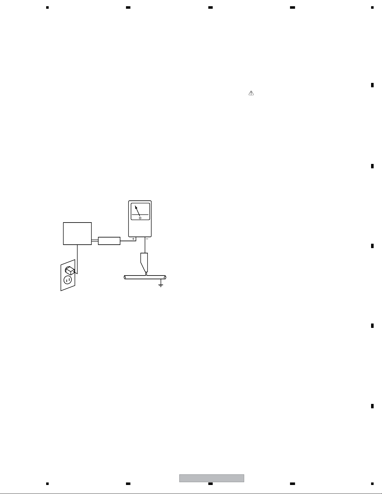
Leakage Current Hot Check
Plug the AC line cord directly into an AC power source (do not
use an isolation transformer for this check).
Turn the AC power switch on.
Using a "Leakage Current Tester (Simpson Model 229
equivalent)", measure for current from all exposed metal parts of
the cabinet (input/output terminals, screwheads, metal overlays,
control shaft, etc.), particularly any exposed metal part having a
return path to the chassis, to a known earth ground (water pipe,
conduit, etc.). Any current measured must not exceed 0.5mA.
PRODUCT SAFETY NOTICE
Many electrical and mechanical parts in PIONEER set have
special safety related characteristics. These are often not evident
from visual inspection nor the protection afforded by them
necessarily can be obtained by using replacement components
rated for higher voltage, wattage, etc. Replacement parts which
have these special safety characteristics are identified in this
Service Manual.
Electrical components having such features are identified by
marking with a on the schematics and on the parts list in this
Service Manual.
The use of a substitute replacement component which dose not
have the same safety characteristics as the PIONEER
recommended replacement one, shown in the parts list in this
Service Manual, may create shock, fire or other hazards.
Product Safety is continuously under review and new instructions
are issued from time to time. For the latest information, always
consult the current PIONEER Service Manual. A subscription to,
or additional copies of, PIONEER Service Manual may be
obtained at a nominal charge from PIONEER.
A
B
C
Reading should
not be above
0.5mA
Earth
ground
Device
under
test
Also test with
plug reversed
(Using AC adapter
plug as required)
Leakage
current
tester
Test all
exposed metal
surfaces
AC Leakage Test
ANY MEASUREMENTS NOT WITHIN THE LIMITS
OUTLINED ABOVE ARE INDICATIVE OF A POTENTIAL
SHOCK HAZARD AND MUST BE CORRECTED BEFORE
RETURNING THE SET TO THE CUSTOMER.
D
E
56
PDP-505PE
F
3
7
8
Page 4
1234
Charged Section
The places where the commercial AC power is used without
A
passing through the power supply transformer.
If the places are touched, there is a risk of electric shock. In
addition, the measuring equipment can be damaged if it is
connected to the GND of the charged section and the GND of the
non-charged section while connecting the set directly to the
commercial AC power supply. Therefore, be sure to connect the
set via an insulated transformer and supply the current.
1. AC Power Cord
2. AC Inlet with Filter
3. Power Switch (S1)
B
4. Fuse (In the POWER SUPPLY Unit)
5. STB Transformer and Converter Transformer
(In the POWER SUPPLY Unit)
6. Other primary side of the POWER SUPPLY Unit
C
: Part is Charged Section.
: Part is the High Voltage Generating Points
other than the Charged Section.
High Voltage Generating Point
The places where voltage is 100V or more except for the charged
places described above. If the places are touched, there is a risk of
electric shock.
1. POWER SUPPLY Unit................................................... (223V)
2. 50 X DRIVE Assy .......................................... (–230V to 223V)
3. 50 Y DRIVE Assy .......................................................... (353V)
4. 50 SCAN A Assy ............................................................ (353V)
5. 50 SCAN B Assy ............................................................(353V)
6. X CONNECTOR AAssy ................................ (–230V to 223V)
7. X CONNECTOR B Assy ............................... (–230V to 223V)
Discharge the VSUS voltage, as shown below:
[Method for discharging the VSUS voltage]
1. Set DRF_SW on the DIGITAL VIDEO Assy to ON (Drive
OFF status). *1, 2
2. Leave the switch at that position for about 20-30 seconds.
3. If the power is on, turn it off. Then return DRF_SW to the OFF
position. *3
Notes
*1: You can also set the unit to "Drive OFF status" by sending the
"DRF" RS232C command from the PC.
*2: DRF_SW can be switched whether the power is on or off.
*3: Power-down will occur if DRF_SW is set to OFF while the
power is on. (See "7.1.6 Power on/off function for the large-
signal system".)
POWER SUPPLY Unit50 Y DRIVE Assy50 SCAN B Assy
D
E
50 SCAN A Assy
AC Inlet with Filter
Power Cord Power Switch
50 X DRIVE Assy
X CONNECTOR
A Assy
X CONNECTOR
B Assy
(S1)
F
4
1234
Fig.1 Charged Section and High Voltage Generating Point (Rear View)
PDP-505PE
Page 5
5678
[Important Check Points for Good Servicing]
In this manual, procedures that must be performed during repairs are marked with the below symbol.
Please be sure to confirm and follow these procedures.
1. Product safety
Please conform to product regulations (such as safety and radiation regulations), and maintain a safe servicing environment by
following the safety instructions described in this manual.
1 Use specified parts for repair.
Use genuine parts. Be sure to use important parts for safety.
2 Do not perform modifications without proper instructions.
Please follow the specified safety methods when modification(addition/change of parts) is required due to interferences such as
radio/TV interference and foreign noise.
3 Make sure the soldering of repaired locations is properly performed.
When you solder while repairing, please be sure that there are no cold solder and other debris.
Soldering should be finished with the proper quantity. (Refer to the example)
4 Make sure the screws are tightly fastened.
Please be sure that all screws are fastened, and that there are no loose screws.
5 Make sure each connectors are correctly inserted.
Please be sure that all connectors are inserted, and that there are no imperfect insertion.
6 Make sure the wiring cables are set to their original state.
Please replace the wiring and cables to the original state after repairs.
In addition, be sure that there are no pinched wires, etc.
7 Make sure screws and soldering scraps do not remain inside the product.
Please check that neither solder debris nor screws remain inside the product.
8 There should be no semi-broken wires, scratches, melting, etc. on the coating of the power cord.
Damaged power cords may lead to fire accidents, so please be sure that there are no damages.
If you find a damaged power cord, please exchange it with a suitable one.
9 There should be no spark traces or similar marks on the power plug.
When spark traces or similar marks are found on the power supply plug, please check the connection and advise on secure
connections and suitable usage. Please exchange the power cord if necessary.
0 Safe environment should be secured during servicing.
When you perform repairs, please pay attention to static electricity, furniture, household articles, etc. in order to prevent injuries.
Please pay attention to your surroundings and repair safely.
A
B
C
D
2. Adjustments
To keep the original performance of the products, optimum adjustments and confirmation of characteristics within specification.
Adjustments should be performed in accordance with the procedures/instructions described in this manual.
3. Lubricants, Glues, and Replacement parts
Use grease and adhesives that are equal to the specified substance.
Make sure the proper amount is applied.
4. Cleaning
For parts that require cleaning, such as optical pickups, tape deck heads, lenses and mirrors used in projection monitors, proper
cleaning should be performed to restore their performances.
5. Shipping mode and Shipping screws
To protect products from damages or failures during transit, the shipping mode should be set or the shipping screws should be
installed before shipment. Please be sure to follow this method especially if it is specified in this manual.
56
PDP-505PE
E
F
5
7
8
Page 6

1234
CONTENTS
SAFETY INFORMATION..................................................................................................................................... 2
1. SPECIFICATIONS ............................................................................................................................................ 7
2. EXPLODED VIEWS AND PARTS LIST ............................................................................................................ 8
A
B
C
D
2.1 PACKING ................................................................................................................................................... 8
2.2 CHASSIS SECTION (1)........................................................................................................................... 10
2.3 CHASSIS SECTION (2)........................................................................................................................... 12
2.4 FRAME SECTION.................................................................................................................................... 14
2.5 MULTI BASE SECTION........................................................................................................................... 16
2.6 REAR SECTION ...................................................................................................................................... 18
2.7 FRONT SECTION.................................................................................................................................... 20
2.8 PANEL CHASSIS (50) Assy (AWU1092) ................................................................................................. 21
2.9 PDP SERVICE Assy 505P (AWU1097) ................................................................................................... 21
3. BLOCK DIAGRAM AND SCHEMATIC DIAGRAM (Refer to “Service Manual: ARP3215”) ............................22
3.1 BLOCK DIAGRAM ................................................................................................................................... 22
3.1.1 OVERALL BLOCK DIAGRAM ........................................................................................................... 22
3.1.2 50 Y DRIVE ASSY............................................................................................................................. 24
3.1.3 50 X DRIVE ASSY............................................................................................................................. 25
3.1.4 PANEL IF ASSY................................................................................................................................. 26
3.1.5 DIGITAL VIDEO ASSY....................................................................................................................... 31
3.1.6 HD AUDIO AMP ASSY...................................................................................................................... 33
3.2 WAVEFORMS.......................................................................................................................................... 34
4. PCB CONNECTION DIAGRAM (Refer to “Service Manual: ARP3215”)
5. PCB PARTS LIST ........................................................................................................................................... 38
6. ADJUSTMENT ............................................................................................................................................... 46
6.1 ADJUSTMENT REQUIRED WHEN THE SET IS REPAIRED OR REPLACED ....................................... 46
6.2 DRIVE ASSY ADJUSTMENT ..................................................................................................................47
6.3 COMMAND .............................................................................................................................................. 48
6.3.1 RS232C COMMAND ......................................................................................................................... 48
6.4 METHOD FOR REPLACING THE SERVICE PANEL ASSY.................................................................... 56
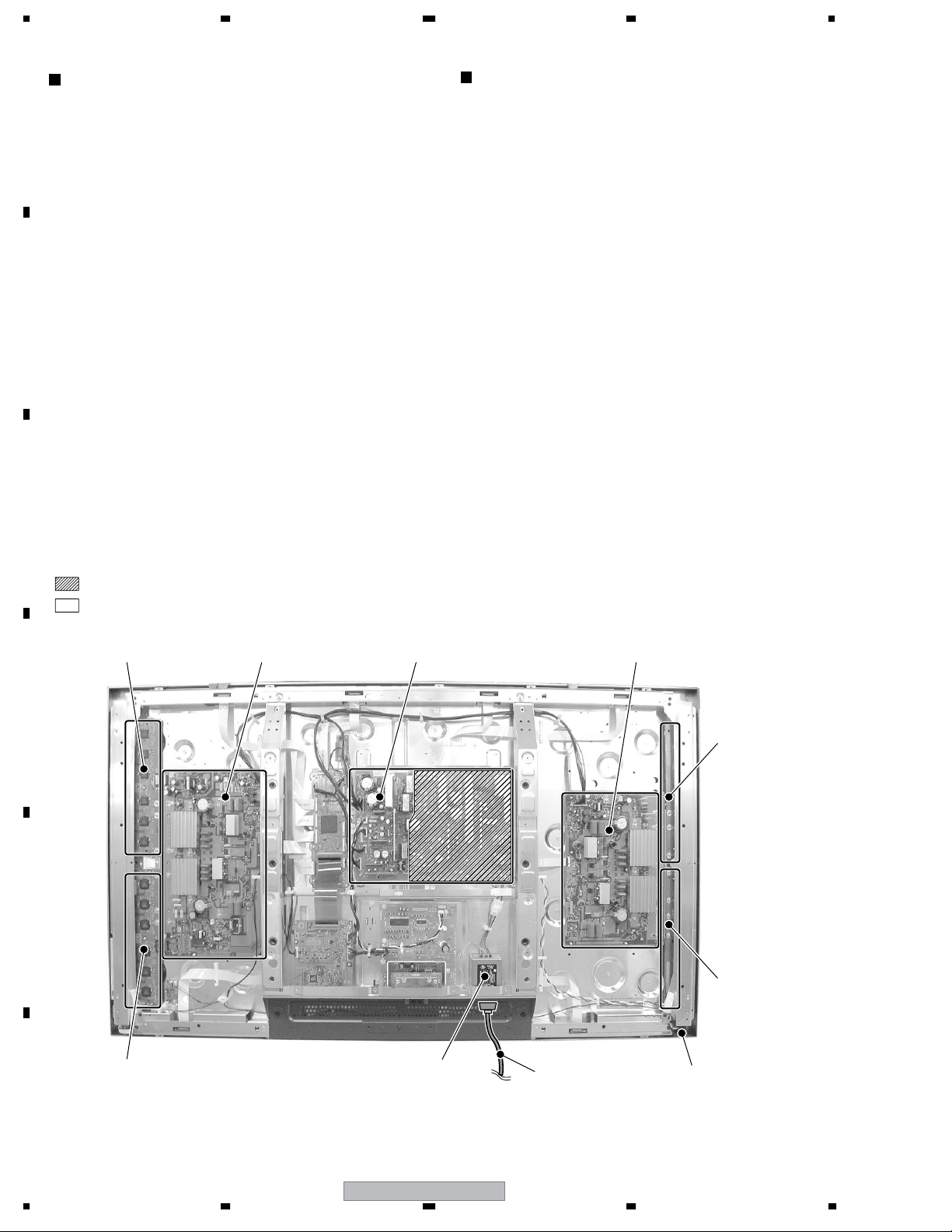
7. GENERAL INFORMATION............................................................................................................................. 57
7.1 DIAGNOSIS ............................................................................................................................................. 57
7.1.1 PCB LOCATION ................................................................................................................................ 57
7.1.2 DIAGNOSIS OF SHUTDOWN/POWER-DOWN INDICATED BY LEDS............................................ 58
7.1.3 DIAGNOSIS WITH THE AID OF FACTORY MODE ..........................................................................63
7.1.4 OPERATION WHEN THE MEDIA RECEIVER IS NOT CONNECTED.............................................. 65
7.1.5 TEMPERATURE-COMPENSATION FUNCTION OF THE DRIVE-SYSTEM VOLTAGE.................... 65
7.1.6 POWER ON/OFF FUNCTION FOR THE LARGE-SIGNAL SYSTEM............................................... 66
7.1.7 BACKUP WHEN THE MAIN UNIT IS ADJUSTED ............................................................................ 67
7.1.8 TROUBLESHOOTING....................................................................................................................... 70
7.1.9 DISASSEMBLY.................................................................................................................................. 71
7.2 IC INFORMATION.................................................................................................................................... 75
8. PANEL FACILITIES ...................................................................................................................................... 101
E
F
6
1234
PDP-505PE
Page 7
5678
1. SPECIFICATIONS
50" Plasma Display
Item
Number of Pixels
Audio Amplifier
Surround System
Power Requirement 220-240V AC,50/60Hz,352W
Dimensions
Weight
Item
Number of Pixels
Audio Amplifier
Surround System
Power Requirement 120V AC,60Hz,363W
Dimensions
Model: PDP-505PE
1280 x 768 pixels
13 W + 13 W (1kHz, 10%, 8Ω)
SRS/FOCUS/TruBass
(0.4W Standby)
1270(W) x 737 (H) x 93 (D) mm
32.8 kg (72.3 lbs.)
Model: PRO-505PU
1280 x 768 pixels
13 W + 13 W (1kHz, 10%, 8Ω)
SRS/FOCUS/TruBass
(0.2W Standby)
1270(W) x 737 (H) x 93 (D) mm
1
/8(W)x 25 11/16(H)x 3 7/8(D)inches)
(44
A
B
C
Weight
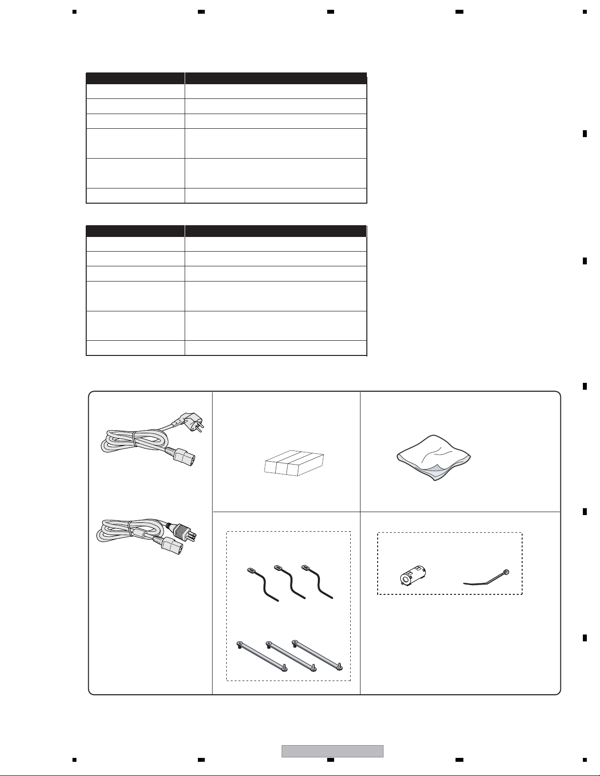
• Accessories
Power Cord
(PDP-505PE: ADG1214)
(PRO-505PU: ADG1215)
32.8 kg (72.3 lbs.)
Speaker Cushion x1
(AEB1384)
(Except PRO-505PU)
Binder Assy (AEC1908)
• Bead Bands x3
• Speed Clamp x3
Wiping Cloth x1
(AED1208)
Ferrite Core
(ATX1039)
(PDP-505PE only)
D
• Cable Tie
E
56
PDP-505PE
F
7
7
8
Page 8
1234
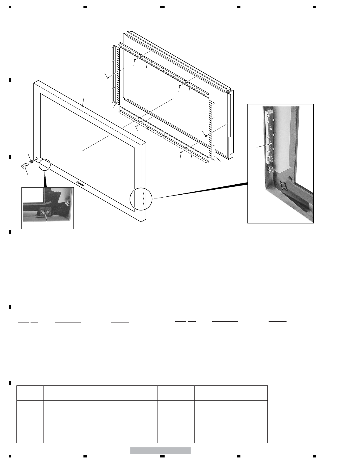
2. EXPLODED VIEWS AND PARTS LIST
NOTES:
Parts marked by "NSP" are generally unavailable because they are not in our Master Spare Parts List.
The mark found on some component parts indicates the importance of the safety factor of the part.
A
Therefore, when replacing, be sure to use parts of identical designation.
Screws adjacent to mark on product are used for disassembly.
For the applying amount of lubricants or glue, follow the instructions in this manual.
(In the case of no amount instructions, apply as you think it appropriate.)
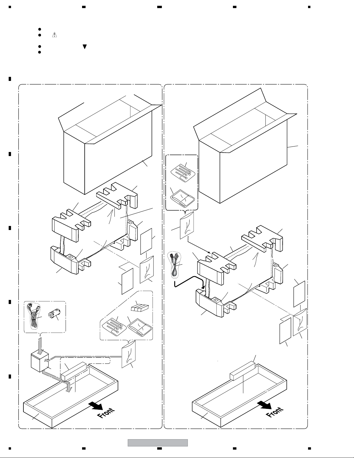
2.1 PACKING
• PDP-505PE / WYVIXK types
B
C
• PRO-505PU / KUC type• PDP-505PE / WYVI
14
4
14
10
9
3
8
12
18
16
8
9
D
11
1
19
E
WYVIXK type only
6
5
7
17
4
3
18, 20
15
2
11
6
10
12
16
15
7
F
13
8
1234
PDP-505PE
13
Page 9
>
>
>
>
5678
PACKING Parts List
No. Description Part No.
Mark
1Power Cord See Contrast table (2)
2Power Cord See Contrast table (2)
3 Wiping Cloth AED1208
4 Binder Assy AEC1908
5 Code Case See Contrast table (2)
No. Description Part No.
Mark
11 Pad See Contrast table (2)
12 Pad See Contrast table (2)
13 Carton (50) See Contrast table (2)
14 Upper Carton See Contrast table (2)
15 Vinyl Bag See Contrast table (2)
A
6 Center Pad (50) See Contrast table (2)
NSP 7 Warranty Card See Contrast table (2)
8 Mirror Mat See Contrast table (2)
9Pad See Contrast table (2)
10 Pad See Contrast table (2)
16 Caution Card ARM1232
17 Speaker Cushion See Contrast table (2)
18 Vinyl Bag S See Contrast table (2)
19 Ferrite Core See Contrast table (2)
20 Poly Bag See Contrast table (2)
(2) CONTRAST TABLE
PDP-505PE/WYVIXK, PRO-505PU/KUC and PDP-505PE/WYVI are constructed the same except for the following :
Mark No. Symbol and Description
1Power Cord ADG1214 ADG1214 Not used
2Power Cord Not used Not used ADG1215
5 Code Case AHC1041 AHC1049 Not used
6 Center Pad (50) Not used AHA2335 Not used
NSP 7 Warranty Card ARY1114 ARY1114 ARY1134
8 Mirror Mat AHG1284 AHG1327 AHG1284
9Pad (50T-L) AHA2366 Not used AHA2366
9Pad (T-L) Not used AHA2381 Not used
10 Pad (50T-R) AHA2367 Not used AHA2367
10 Pad (T-R) Not used AHA2382 Not used
PDP-505PE
WYVI
PDP-505PE
WYVIXK
PRO-505PU
KUC
B
C
11 Pad (50B-L) AHA2368 Not used AHA2368
11 Pad (B-L) Not used AHA2383 Not used
12 Pad (50B-R) AHA2369 Not used AHA2369
12 Pad (B-R) Not used AHA2384 Not used
13 Carton (50) AHD3177 AHD3191 AHD3177
14 Upper Carton (505PE) AHD3265 Not used Not used
14 Upper Carton (50) Not used AHD3271 Not used
14 Upper Carton (50EL) Not used Not used AHD3281
15 Vinyl Bag AHG1340 Not used AHG1340
17 Speaker Cushion AEB1384 AEB1384 Not used
18 Vinyl Bag S AHG1338 Not used AHG1338
19 Ferrite Core ATX1039 ATX1039 Not used
20 Poly Bag Not used AHG1326 Not used
D
E
F
56
PDP-505PE
9
7
8
Page 10
1234
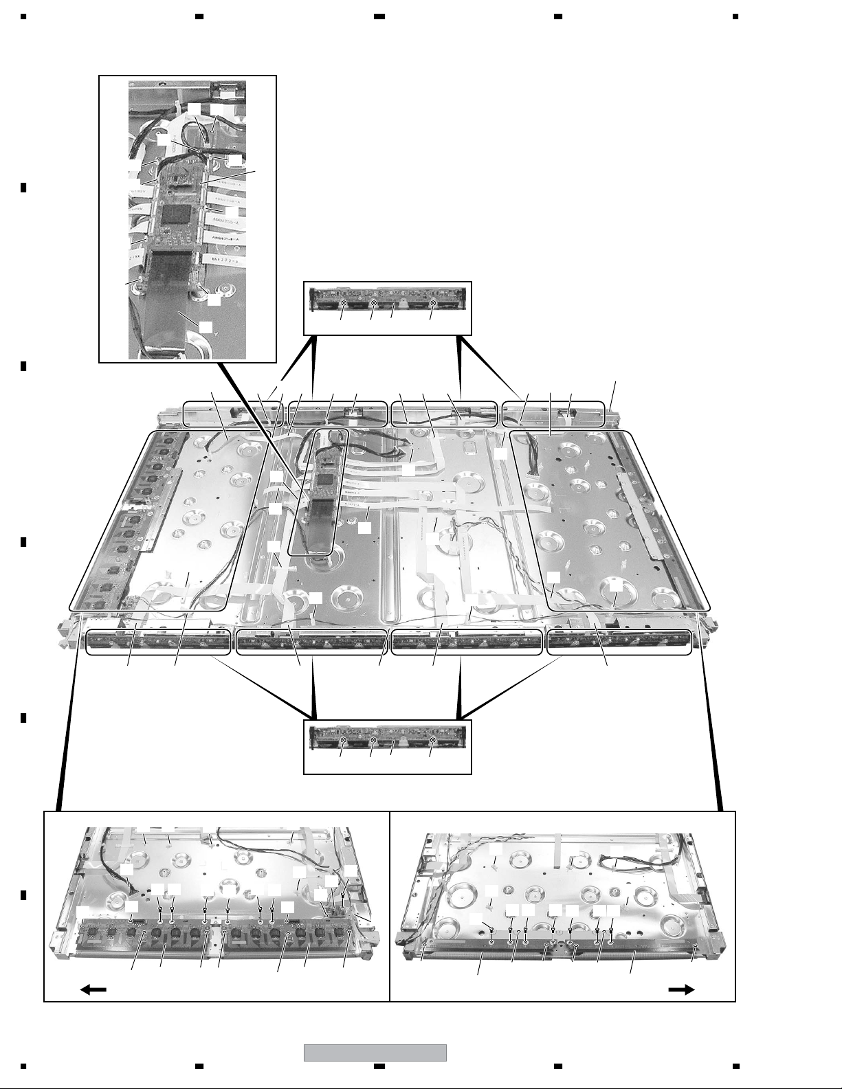
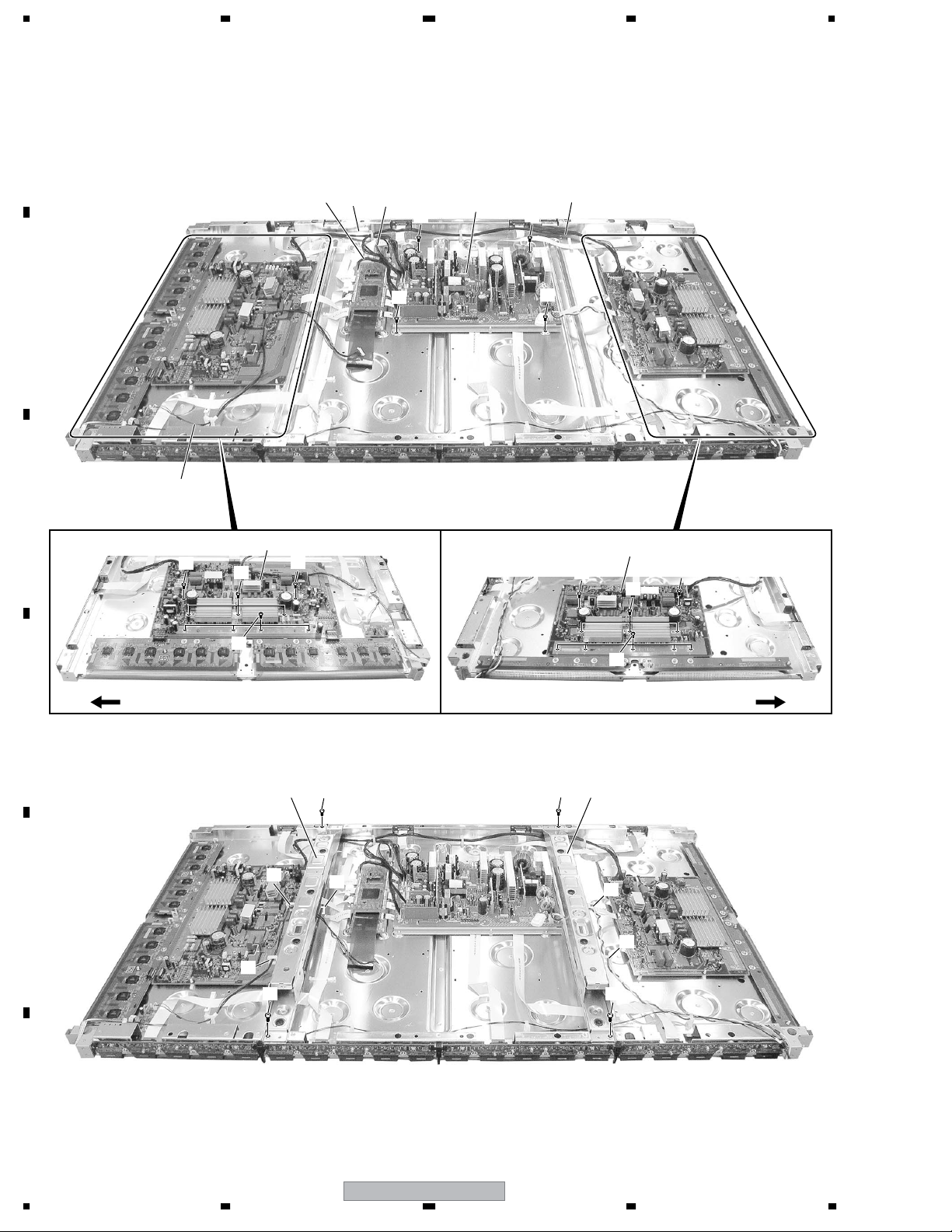
2.2 CHASSIS SECTION (1)
A
23
24
23
B
C
23
30
8
30
23
1
23
23
10
31 31 31
2734 22 11 27
22
3
2
143422 132727 12
22
28
19
20
22
22
27
D
15 16 27 17 1827
31 31 31
E
33
26
23
23
28
32
9
29
26
232324
26
23
3333 33
33
33
28
22
27
3
33
23
23
33 33 33
23
33 3333
27
23
23
2525
5
Upper
F
side
25
26 26 26
10
1234
25
4
7
PDP-505PE
25 3535 25
6
Upper
side
Page 11

5678
CHASSIS SECTION (1) parts List
No. Description Part No.
Mark
1 DIGITAL VIDEO Assy AWV2074
NSP 2 P. Chassis (505) Assy AWU1092
NSP 3 50 ADDRESS Assy AWZ6870
NSP 4 50 SCAN A Assy AWZ6878
NSP 5 50 SCAN B Assy AWZ6879
NSP 6 X CONNECTOR A Assy AWZ6880
NSP 7 X CONNECTOR B Assy AWZ6881
8PANEL SENSOR Assy AWZ6872
9 KEY CONTROL Assy AWZ6844
10 FPC (114P) ADY1088
11 Flexible Cable (J201) ADD1248
12 Flexible Cable (J202) ADD1249
13 Flexible Cable (J203) ADD1250
14 Flexible Cable (J204) ADD1251
15 Flexible Cable (J205) ADD1252
16 Flexible Cable (J206) ADD1253
17 Flexible Cable (J207) ADD1254
18 Flexible Cable (J208) ADD1255
19 Flexible Cable (J209) ADD1270
20 Flexible Cable (J210) ADD1271
21 • • • • •
22 Flat Clamp AEC1879
23 PCB Spacer AEC1941
24 PCB Support AEC1938
25 PCB Spacer AEC1944
26 PCB Support AEC1958
27 Wire Saddle AEC1745
28 PCB Spacer AEC1947
29 Wire Clip AEC1948
30 Nylon Rivet AEC1671
31 Screw VBB30P080FNI
32 Screw ABZ30P060FTC
33 Screw PMB30P060FNI
34 Rear corner label AAX3081
35 Card Spacer AEC2013
A
B
C
D
56
PDP-505PE
E
F
11
7
8
Page 12
1234
2.3 CHASSIS SECTION (2)
A
13
13
6
2
15
15
12
15
4
5
8
13
B
7
C
3
15
15
12
15
13
1
Upper
side
D
14
14
11
E
11
14
F
11
109
11
11
14
Upper
side
12
PDP-505PE
1234
Page 13

>
5678
CHASSIS SECTION (2) parts List
No. Description Part No.
Mark
1POWER SUPPLY Unit AXY1085
2 50 X DRIVE Assy AWZ6877
3 50 Y DRIVE Assy AWV2082
4 Wire A (J101) ADX2945
5 11P Housing Wire (J102) ADX2950
6 12P Housing Wire (J103) ADX2951
7 9P Housing Wire (J106) ADX2949
8 3P Housing Wire (J109) ADX2948
9 SUB Frame L Assy (50P) ANG2638
10 SUB Frame R Assy (50P) ANG2561
11 Wire Saddle AEC1745
12 Screw PMB30P060FNI
13 Screw ABZ30P060FTC
14 Screw AMZ30P080FTC
15 Screw VBB30P080FNI
A
B
C
D
E
56
PDP-505PE
F
13
7
8
Page 14
1234
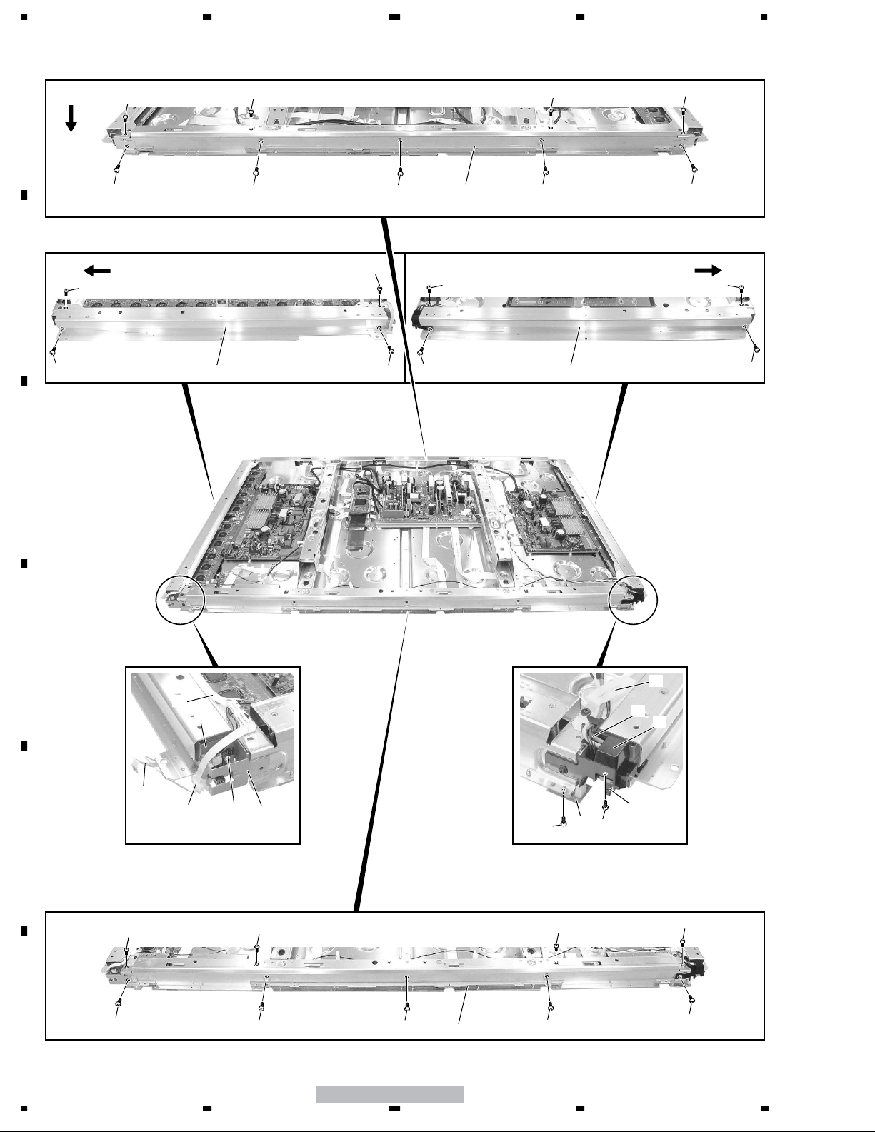
2.4 FRAME SECTION
A
Upper
side
Upper
side
B
17
C
17
17
17
16
1515
17
17
17
8 9
17
16
156
17
17
17
Upper
side
17
D
10
11
1
5
14
E
17
F
17
16
15
1318
15
7
18
2
16
15
4
12
3
15
17
17
14
PDP-505PE
1234
Page 15

5678
FRAME SECTION parts List
No. Description Part No.
Mark
1PANEL IR Assy AWZ6845
2PANEL LED Assy AWZ6842
3Power Switch (S1) ASG1092
4 Housing Wire (50)(J110) ADX2964
5 Flexible Cable (J211) ADD1225
6Front Chassis HU Assy (50) ANA1792
7Front Chassis HD Assy (50) ANA1793
8Front Chassis VL (50) ANA1794
9Front Chassis VR (50) ANA1795
10 Clamp AEC1884
11 Flat Clamp AEC1879
12 Switch Holder AMR3402
13 IR Holder ANG2665
14 Wire Clip AEC1948
15 Screw BPZ30P080FTB
16 Screw AMZ30P080FTC
17 Screw AMZ30P060FTB
18 Screw ABZ30P060FTC
>
A
B
C
D
E
56
PDP-505PE
F
15
7
8
Page 16
1234
2.5 MULTI BASE SECTION
A
Back side
12
(Note)
12
(Note)
(Note)
12
12
12
(Note)
Note:
The No. 12 parts must be
inserted from the front
9
surface.
9
B
15
13
16
5211 14
Front side
C
D
4 615
13
13
15
17 17
7
(Note)
20
Note: When servicing, be sure to glue on the Gasket (AU)
E
17
17
17
F
16
1234
18 19
17
PDP-505PE
17
17
17
8
and make sure that they won't peel off.
(Note)
20
17
17
21
17
17
17
Page 17

5678
MULTI BASE SECTION parts List
No. Description Part No.
Mark
1PANEL IF Assy AWZ6841
2 HD AUDIO AMP Assy AWZ6863
3 HD SP TERMINAL Assy AWZ6864
4AC Inlet (CN1) AKP1263
5 3P/8P Housing Wire (J104) ADX2922
6 13P Housing Wire (J105) ADX2947
7 Multi Base (P) Assy ANA1786
8 Under Cover Assy ANG2589
9 Locking Card Spacer V0 AEC2005
10 • • • • •
11 Clamp AEC1884
12 PCB Spacer AEC1941
13 HL 18 AEC1980
14 SB Spacer AEC2002
NSP 15 Wire Saddle AEC1745
16 Screw PMB30P060FNI
17 Screw AMZ30P060FTB
18 Hexagon Headed Screw BBA1051
19 Screw PMZ26P060FTB
20 Gasket (AU) ANK1745
21 Screw BPZ30P080FTB
>
A
B
C
D
E
F
56
PDP-505PE
17
7
8
Page 18
1234
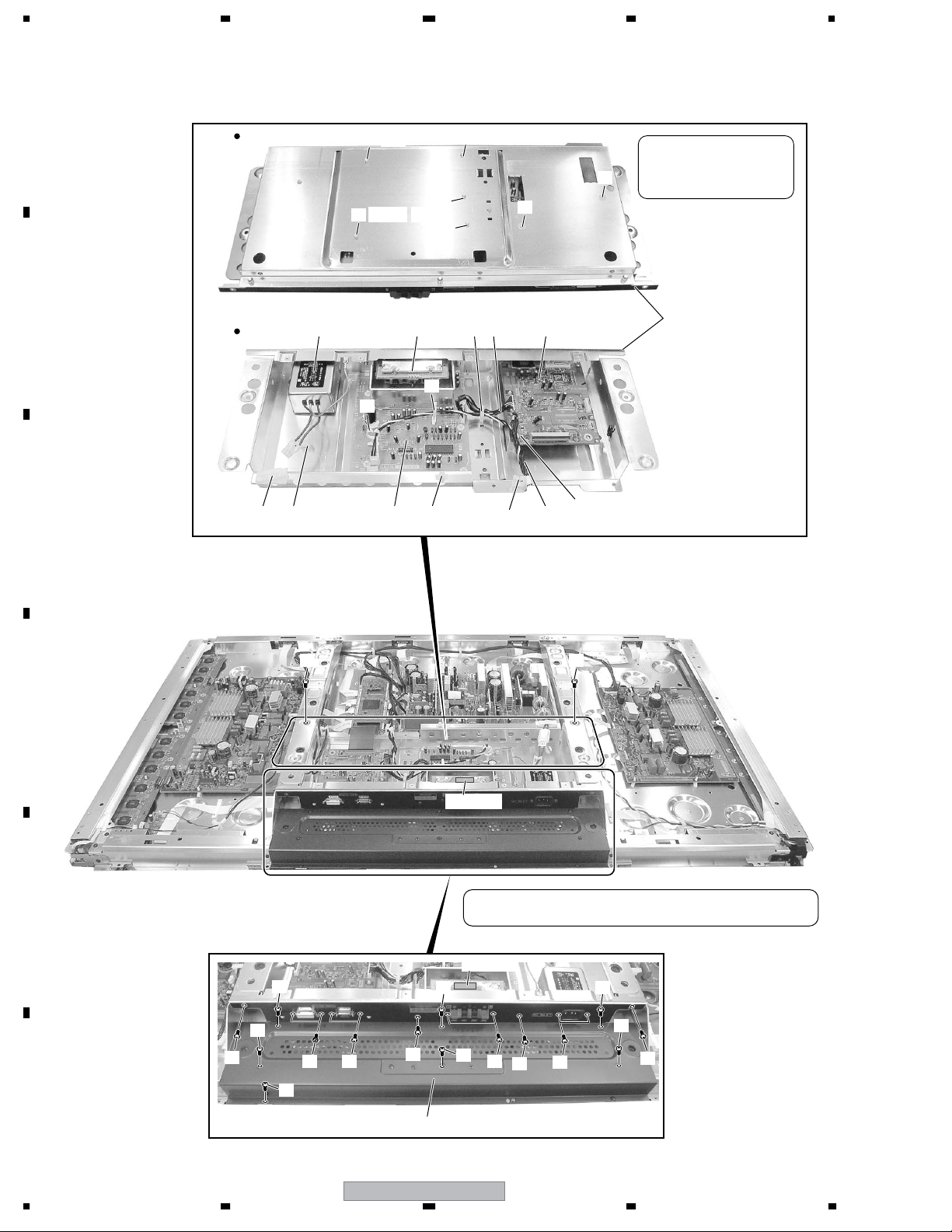
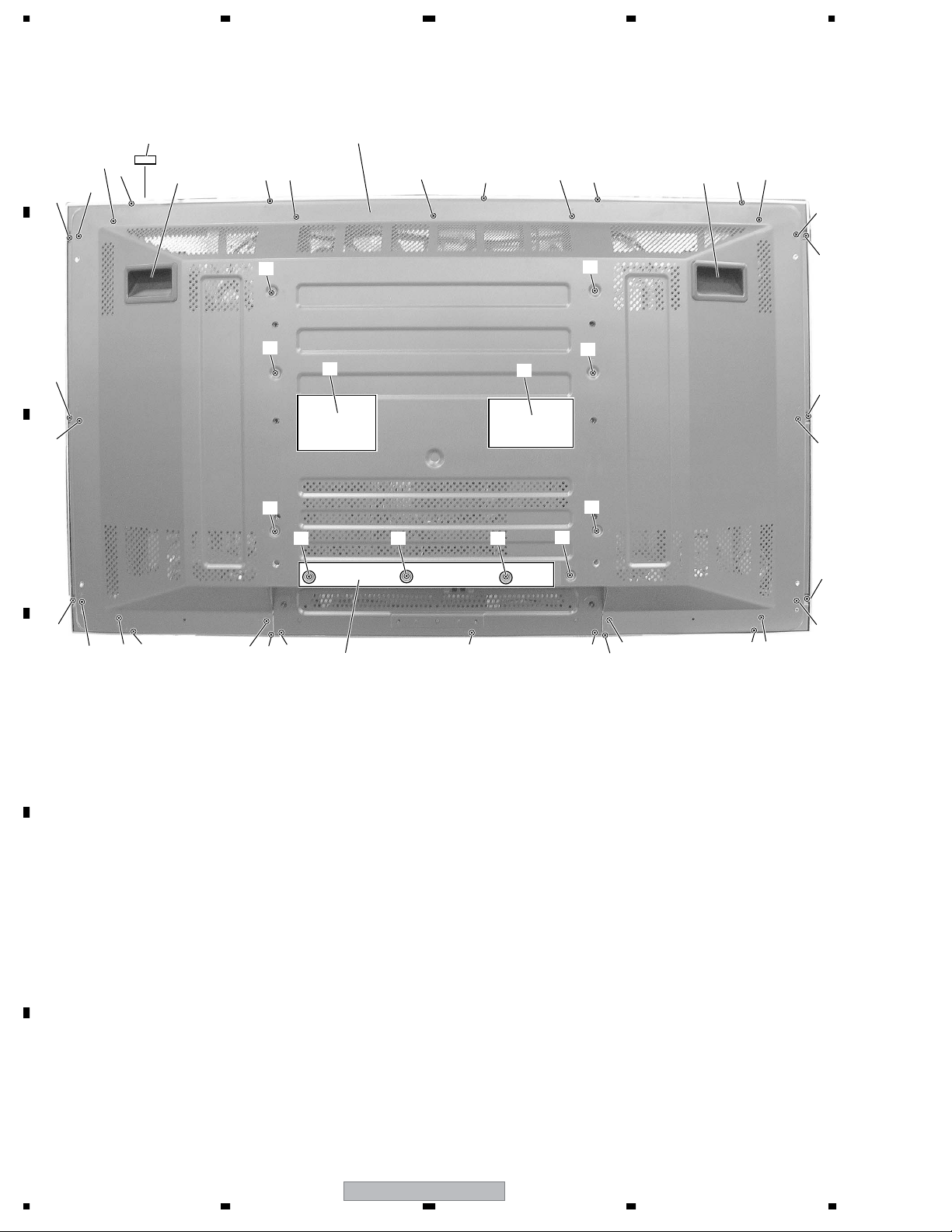
2.6 REAR SECTION
A
7
8
6
8
6
2 2
1
6
8
8
6
8
6
8
6
8
8
B
8
6
8
C
6
6
8
8
8
8 6
3
8 8
6 6
5
8
4
8
8
8
8
8
6
6
8
6
6
6
8
6
8
D
E
F
18
PDP-505PE
1234
Page 19
5678
REAR SECTION parts List
No. Description Part No.
No. Description Part No.
Mark
1 Rear Case (50P) ANE1626
2 Inner Grip Assy AMR3434
NSP 3 Name Label See Contrast table (2)
4Volt caution Label See Contrast table (2)
5Terminal Label See Contrast table (2)
Mark
6 Screw ABZ30P100FTB
7 Serial Sheet AAX3143
8 Screw AMZ30P060FTB
(2) CONTRAST TABLE
PDP-505PE/WYVIXK, PRO-505PU/KUC and PDP-505PE/WYVI are constructed the same except for the following :
Mark No. Symbol and Description
NSP 3 Name Label AAL2568 AAL2580 AAL2570
4Volt Caution Label AAX3117 AAX3005 AAX3117
5Terminal Label AAX2998 AAX3006 AAX2997
PDP-505PE
WYVI
PDP-505PE
WYVIXK
PRO-505PU
KUC
A
B
C
D
E
56
PDP-505PE
F
19
7
8
Page 20
1234
2.7 FRONT SECTION
A
8
2
4
B
6
3
• Rear view
C
7
8
5
8
5
8
5
8
8
1
5
4
D
FRONT SECTION parts List
No. Description Part No.
No. Description Part No.
Mark
1PANEL KEY Assy AWZ6843
2Front Case Assy See Contrast table (2)
3Power Button AAD4127
E
NSP 4 Panel Holder V (50) ANG2663
5Panel Holder H Assy 50 See Contrast table (2)
Mark
6 Coil Spring ABH1114
7 Blind Cushion AEB1383
8 Screw ABZ30P060FTC
(2) CONTRAST TABLE
PDP-505PE/WYVIXK, PRO-505PU/KUC and PDP-505PE/WYVI are constructed the same except for the following :
Mark No. Symbol and Description
2Front Case Assy (50PE) AMB2834 AMB2834 Not used
2Front Case Assy (50EL) Not used Not used AMB2836
F
5Panel Holder H Assy 50 ANG2678 Not used ANG2678
5Panel Holder H Not used ANG2662 Not used
5 Gasket Not used ANK1740 Not used
PDP-505PE
WYVI
PDP-505PE
WYVIXK
PRO-505PU
KUC
20
PDP-505PE
1234
Page 21
5678
2.8 PANEL CHASSIS (50) Assy (AWU1092)
PANEL CHASSIS (50) Assy (AWU1092) parts List
No. Description Part No.
Mark
NSP 1..50 ADDRESS Assy AWV2080
NSP 2..50 ADDRESS Assy AWZ6870
NSP 1..50 SCAN Assy AWV2083
NSP 2..50 SCAN A Assy AWZ6878
NSP 2..50 SCAN B Assy AWZ6879
NSP 2..X CONNECTOR A Assy AWZ6880
NSP 2..X CONNECTOR B Assy AWZ6881
NSP P. Panel (50LC) Assy AWU1103
NSP Adress Module (IC1-IC40) AXF1129
NSP FPC (50XGA-X) ADY1084
NSP FPC (50XGA-Y) ADY1085
NSP Chassis Assy (505) ANA1803
PCB Spacer AEC1944
PCB Support AEC1958
Edge Card Spacer AEC1998
Mark
Rivet (Plastic) AMR1066
FC Spacer AMR3370
NSP Adhesive ZBA-KE3424S
NSP Lotion ZLX-AP7
NSP Tape ZTA-8101-12
NSP Double Faced Tape ZTB-5015-18
NSP Tape ZTC-POLYCA-20
NSP Tape ZTC-900UL-15
NSP Silicone Rubber ZTX-HC20-15
NSP Silicone Rubber ZTX-HC50-15
NSP Wiping Cloth ZTX-MX100-13
NSP Film
NSP Film ZTX-2102Y45-5
No. Description Part No.
NSP Silicone Rubber
A
ZTC-EM7KB0R85T-15W
B
ZTX-2102Y35-2R5
2.9 PDP SERVICE Assy 505P (AWU1097)
PDP SERVICE Assy 505P (AWU1097) parts List
NSP 1..P.Chassis (505) Assy AWU1092
1..Front Chassis HU Assy (50) ANA1792
1..Front Chassis HD Assy (50) ANA1793
1..Front Chassis VL (50) ANA1794
1..Front Chassis VR (50) ANA1795
1..Sub Frame L Assy (50P) ANG2638
1..Sub Frame R Assy (50P) ANG2561
1..Wire Saddle AEC1745
1..PCB Support AEC1938
1..PCB Spacer AEC1941
1..PCB Spacer AEC1947
1..Wire Clip AEC1948
1..Card Spacer AEC2013
1..Caution Label AAX3031
1..Drive Voltage Label ARW1097
1..Screw ABZ30P100FTB
1..Screw AMZ30P060FTB
1..Screw AMZ30P080FTC
1..Screw VBB30P080FNI
1..Screw BPZ30P080FTB
NSP 1..Front Case Assy (50SVC) AMB2849
2..Panel Cushion H (50) AED1257
2..Panel Cushion V (50) AED1258
NSP 2..Front Case (50P) AMB2823
1..Rear Case (50P) ANE1614
NSP 1..Vinyl Pouch AHG-195
1..Pad (50T-L) AHA2366
1..Pad (50T-R) AHA2367
1..Pad (50B-L) AHA2368
1..Pad (50B-R) AHA2369
1..Carton(50) AHD3177
1..Upper Carton (505SVC) AHD3290
1..Protect Sheet AHG1331
1..Rear corner label(15) AAX3081
C
D
E
F
56
PDP-505PE
21
7
8
Page 22
1234
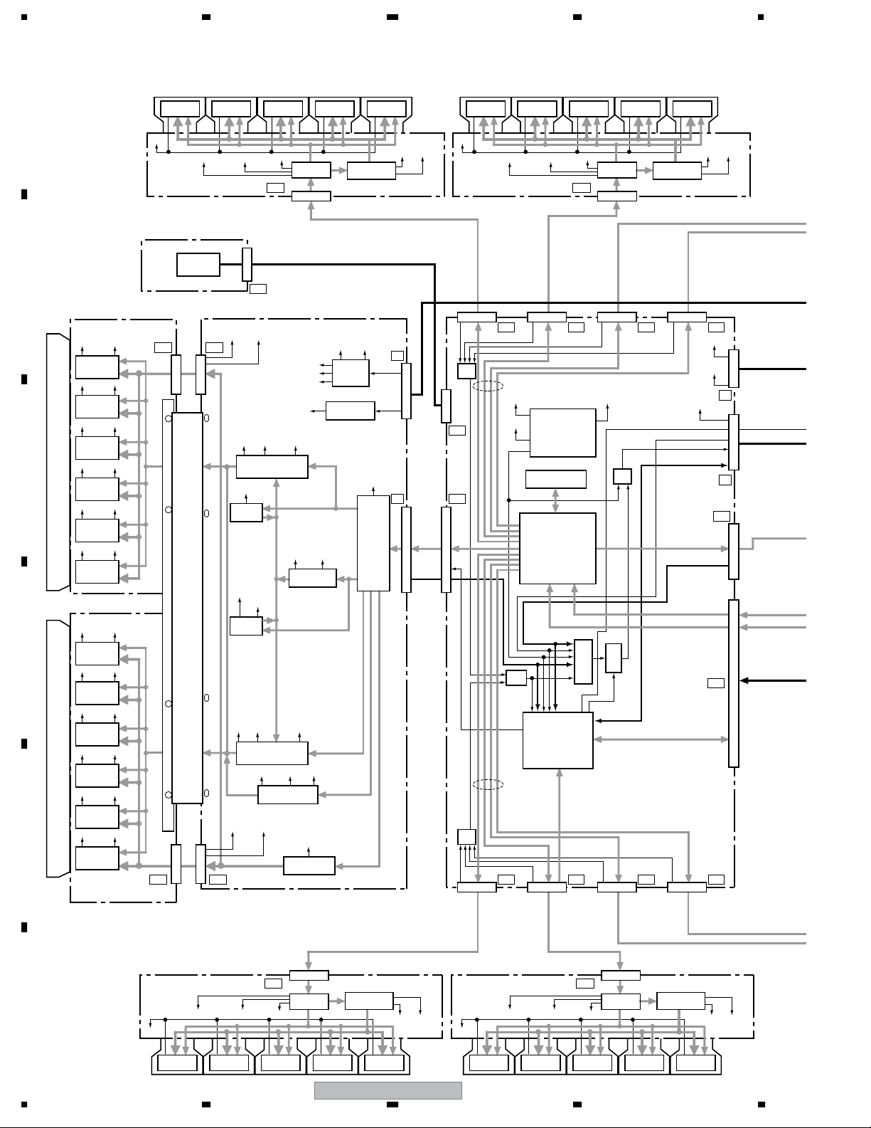
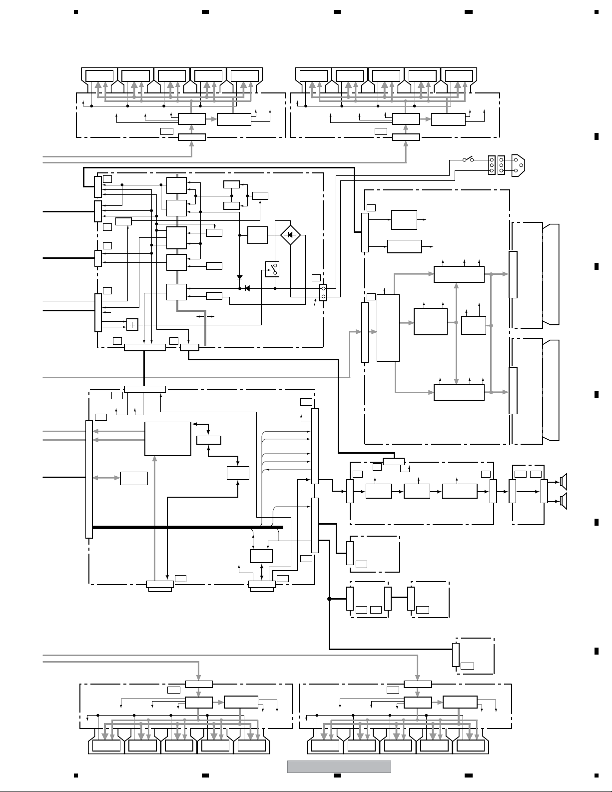
3. BLOCK DIAGRAM AND SCHEMATIC DIAGRAM
3.1 BLOCK DIAGRAM
3.1.1 OVERALL BLOCK DIAGRAM
A
DRIVER IC
IC1551
DRIVER IC
IC1552
DRIVER IC
IC1553
DRIVER IC
IC1554
DRIVER IC
IC1555
DRIVER IC
IC1551
DRIVER IC
IC1552
DRIVER IC
IC1553
DRIVER IC
IC1554
DRIVER IC
IC1555
V+5V
V+3V_IC5
V+3V_PLLV+3V_LVDS
AD1
IC1501
CN1501
V+ADR
RESONANCE
50 ADDRESS ASSY
V+9V
BLOCK
V+60V
V+5V
V+9V
V+3V_IC5
V+3V_PLLV+3V_LVDS
AD1
IC1501
CN1501
V+ADR
RESONANCE
BLOCK
50 ADDRESS ASSY
V+60V
PANEL SENSOR ASSY
SENSOR
IC1072
B
50 SCAN B ASSY
VCC
_VH
VCC
_VH
VCC
_VH
VCC
_VH
VCC
_VH
VCC
_VH
VCC
_VH
VCC
_VH
VCC
_VH
VCC
_VH
VCC
_VH
VCC
_VH
PSUS
PSUS
SB1 Y2
SCAN
CN3201
SCAN
CN3001
SA1 Y3
CN2101
CN2102
IC5V
ADD
SEL_PULSE
IC3201
IC5V
ADD
SEL_PULSE
IC3202
IC5V
ADD
SEL_PULSE
IC3203
C
D
E
IC5V
ADD
SEL_PULSE
IC3204
IC5V
ADD
SEL_PULSE
IC3205
IC5V
ADD
SEL_PULSE
IC3206
IC5V
ADD
SEL_PULSE
IC3001
IC5V
ADD
SEL_PULSE
IC3002
IC5V
ADD
SEL_PULSE
IC3003
IC5V
ADD
SEL_PULSE
IC3004
IC5V
ADD
SEL_PULSE
IC3005
IC5V
ADD
SEL_PULSE
IC3006
50 SCAN A ASSY
CN1071
TE1
V_IC5V
VCC_VH
+16.5V
+5V
PSUSPSUS
MASK MOD
IC2307
+16.5V
SOFT-D
BLOCK
+16.5V
VSUS
+RESET
BLOCK
+5V +15V VSUS
MASK MOD
+5V +16.5V V_OFS
VCC_VH
V_IC5V
Scan Signal
50 Y DRIVE ASSY
V_OFS
VC_VF-
VC_VF+
+5V
VSUS
Drive
Signal
+5V
+16.5V
RESONANCE
BLOCK
IC2303
OFFSET
BLOCK
V_IC5V
Photo Coupler
BLOCK
DC_DC
CONV
BLOCK
REGULATOR
Drive
Signal
Drive
Signal
V_IC5VVCC_VH
LOGIC
BLOCK
VSUS
+5V
Y4
CN2301
+6.5V
Y1 D13
SCAN
YSUS
CN2001
VH_UV_PD
YDRIVE_PD
YRESNC_PD
YDD_CHV_PD
IC5V_UV_PD
CN5501
ADR_
PD0
OR
CN5202
D4
CN5521
OR
ADR_
PD4
CN5505
D5
ADR_PD1
LVDS
V+3V_D
V+1V_D
DCC_PD
FLASH MEMORY
SUB-FILD CONV.
XY DRV SEQUENCE
PATTERN GEN.
OR
Vofs
MODULE UCOM
LVDS
ADR_PD5
D9
CN5502
D6
ADR_PD2
CN5503
DIGITAL VIDEO ASSY
V+12V
DC-DC
CONVERTER
MODULE
AXY1086
IC5305
IC5401
PEG054A
IC5201
CN5506
&
PSIZU
ADR_PD6
D10
OR
OR
PD_MUTE
RELAY, PD_TRIGGER
CN5507
D7
ADR_PD3
PD
ADR_PD7
D11
CN5504
V+60V
V+6.5V
V+12V
Vsus_ADJ.
PD_PWDN
XSUS
XSUSTN_PD
XDD_CNV_PD
XDRIVE_PD
DCLK, DE
HD, VD
RA IN, GA IN, BA IN
RB IN, GB IN, BB IN
CN5508
D8
D15
D12
D2
CN5601 CN5602
D1
D14
CN5511
CN5001
CN1501
AD1
V+3V_PLLV+3V_LVDS
F
V+5V
DRIVER IC
IC1551
DRIVER IC
IC1552
V+3V_IC5
DRIVER IC
IC1553
22
50 ADDRESS ASSY
DRIVER IC
IC1554
RESONANCE
BLOCK
V+ADR
IC1501
PDP-505PE
V+9V
DRIVER IC
IC1555
V+60V
V+5V
DRIVER IC
IC1551
V+3V_PLLV+3V_LVDS
DRIVER IC
IC1552
AD1
V+3V_IC5
DRIVER IC
IC1553
CN1501
50 ADDRESS ASSY
DRIVER IC
IC1554
RESONANCE
V+ADR
IC1501
BLOCK
DRIVER IC
IC1555
V+9V
V+60V
1234
Page 23
5678
DRIVER IC
IC1551
V+5V
RA IN, GA IN, BA IN
RB IN, GB IN, BB IN
CN4004
DRIVER IC
IC1552
V+3V_PLLV+3V_LVDS
P4
VSUS
+6.5V
+16.5V
M601
VSUS_
P3
CONT
P5
+6.5V
VADR
P2
Vsus_ADJ.
+12V
PS.PD
EXT.PD
RELAY
STB
3.3V
P1 P6
CN4001
R1
V+3V
V+6.5V
ACTV
R4
DCLK, DE
HD, VD
EEPROM
for Backup
B_SDA
B_SCL
DRIVER IC
V+3V_IC5
AD1
SECONDARY
+6.5V
TMDS RECEIVER
IC4202
TMDS
CN4003
IC1553
STB3.3
MUTE
DDC
DRIVER IC
IC1501
CN1501
T5
T4
T2
T3
T1
PANEL IF ASSY
FET SW
R3
IC1554
DRIVER IC
V+ADR
RESONANCE
BLOCK
IC1555
V+9V
V+60V
50 ADDRESS ASSY
Switching
Q14
Q13
+390V
D133
D31,D32
M341
PFC
Q1,Q2
RL1
RELAY
& PD
Switching
Q11
Switching
Q12
Switching
M1
Switching
PRIMARY
POWER SUPPLY UNIT
A_SCL,A_SDA,SRS
Bus
Buffer
Bus
V+3V_STB
Buffer
CN4002
MDR CONNECTORDVI CONNECTOR
V+5V
RC1
NEUTRAL
V+6.5V
FOCUS,TRUBASS
A_MUTE
ST_BY
A_NG
AUDIO L
AUDIO R
LED_R,G
KEY
REM
STB
_MT
R2
DRIVER IC
IC1551
P7
LIVE
R7
CN4009
CN4010
R8
DRIVER IC
IC1552
DRIVER IC
IC1553
V+3V_IC5
V+3V_PLLV+3V_LVDS
AD1
DRIVER IC
IC1554
V+ADR
IC1501
CN1501
RESONANCE
50 ADDRESS ASSY
LIVE
NEUTRAL
DRIVER IC
IC1555
BLOCK
MAIN POWER
V+9V
S1
V+60V
50 X DRIVE ASSY
X2
DC_DC
VSUS
CONV
BLOCK
+6.5V
REGULATOR
Drive
+5V
Signal
X1
LOGIC
BLOCK
CN1001 CN1201
CN3504
A4
+9V
A1 A3 SP2 SP1
L,R
WOW IC
IC3501
L,R
Drive
Signal
+16.5V
RESONANCE
BLOCK
+16.5V
+9V
VOL IC
IC3502
V_RN
+5V
+16.5V
MASK MOD
IC1203
V_RN
-RESET
+16.5VVSUS
IC1207
+16.5V
IC3504
+16.5V
PULSE
BLOCK
+5V
+5V
VSUS
SUS
OUT
+5V
SUS
OUT
MASK MOD
L,R L,R
POWER AMP
PSUS
PSUS
L,R L,R
CN3503
HD AUDIO AMP ASSY
PANEL
LED
CN4751 CN3501
ASSY
L1
CN4852
KL2 KL1 SW1
KEY CONTROL
ASSY
CN4851
CN4801
PANEL KEY
ASSY
PANEL IR
CN4901
RE1
ASSY
AC INLET
X CONNECTOR
A ASSY
X CONNECTOR
B ASSY
J3701
CN3701
HD SP TERMINAL
ASSY
A
B
C
D
SPEAKER
E
V+5V
DRIVER IC
IC1551
CN1501
V+3V_PLLV+3V_LVDS
DRIVER IC
IC1552
AD1
V+3V_IC5
DRIVER IC
IC1553
50 ADDRESS ASSY
DRIVER IC
IC1554
RESONANCE
BLOCK
V+ADR
IC1501
DRIVER IC
IC1555
V+9V
V+60V
V+5V
DRIVER IC
IC1551
V+3V_PLLV+3V_LVDS
DRIVER IC
IC1552
PDP-505PE
56
AD1
V+3V_IC5
DRIVER IC
IC1553
7
CN1501
50 ADDRESS ASSY
DRIVER IC
IC1554
RESONANCE
V+ADR
IC1501
BLOCK
DRIVER IC
IC1555
V+9V
V+60V
F
23
8
Page 24
1234
3.1.2 50 Y DRIVE ASSY
• Block Diagram
A
50 Y DRIVE ASSY
Y1
IC5V
VH
Y2
To
50 SCAN B ASSY
CN2101CN2102
CE
B
C
D
CLK2
CLR
OC2
OC1
YPR-U
YSOFT-D
YSUS-G
YSUS-B
YSUS-U2
From DIGITAL VIDEO ASSY
YSUS-D2
YSUS-U1
YSUS-D1
YSUS-MSK
YOFS
YSUS-PD
SCN_5V_PD
Y_DD_PD
SCAN_PD
YDRIVE_PD
Photo CouplerCLK1
Photo Coupler
Photo Coupler
Photo Coupler
Photo Coupler
Photo Coupler
SI
Photo Coupler
CN2001
VH
Y3
YSUS
-U2
5V
YSUS-D2
YSUS-U1
5V
YSUS-D1
To
50 SCAN A ASSY
YPR-U
YSOFT-D
IC2202
HB
DRIVER
SUS
HB
XSUS
P.D.
Circuit
GND
SUS
GND
IC2201
DRIVER
IC2203
YSUS-G
YSUS-B
L2204
L2202
VSUS
L2205
L2203
VSUS
16.5V
VSUS
16.5V
5V
5V
Mask Module
IC2303
STK795-513A
Mask Module
IC2307
STK795-513A
To
SCAN ASSY
YSUS-MSK
YOFS
IC2302
Photo
Coupler
IC2304
IC2311
E
Y4
CN2301
1
16.5V
2
DGND
3
6.5V
DGND
4
N.C.
5
6
N.C.
7
VSUS VSUS
VSUS
8
N.C.
9
F
SUSGND
SUSGND
From POWER SUPPLY UNIT
10
11
P.D.
DET.
IC2305
REGULATOR
IC5V UVP
5V
VOFS OVP
VOFS UVP
VH OVP
VH UVP
VSUS
IC5V, VF
D-D CONV.
D-D CONV.
VH D-D
CONV.
24
VOFS
VF+
VF-
IC5V
VOFS
VH
PDP-505PE
1234
Page 25
5678
3.1.3 50 X DRIVE ASSY
• Block Diagram
A
X1
XSUS-G
XSUS-B
XSUS-U2
XSUS-D2
XSUS-U1
XSUS-D1
XSUS-MSK
XCP-MSK
XSUS_PD
XDD_PD
XDRV_PD
From DIGITAL VIDEO ASSY
SUSGND
SUSGND
From POWER SUPPLY UNIT
CN1001
XNR-D
X2
CN1201
1
16.5V
2
DGND
3
6.5V
DGND
4
N.C.
5
6
N.C.
7
VSUS VSUS
VSUS
8
N.C.
9
10
11
12
N.C.
50 X DRIVE ASSY
P.D.
DET.
IC1205
REGULATOR
5V
VRN UVP P.D.
XNR-D
VRN OVP
P.D.
XSUS
-U2
5V
XSUS-D2
XSUS-U1
5V
XSUS-D1
XCP-MSK
XSUS-MSK
VSUS
D-D CONV.
T1401
IC1101
HB
DRIVER
IC1102
HB
DRIVER
XSUS
P.D.
Circuit
Charge Pump
Circuit
IC1202
Photo
Coupler
IC1204
VRN-235V
SUS
GND
SUS
GND
VCP
XSUS-G
XSUS-B
L1102
L1104
L1103
L1105
VSUS
16.5V
VSUS
16.5V
5V
5V
Mask Module
IC1203
STK795-512A
Mask Module
IC1207
STK795-512A
PSUS
To
X CONNECTOR ASSY
B
C
D
56
PDP-505PE
E
F
25
7
8
Page 26
1234
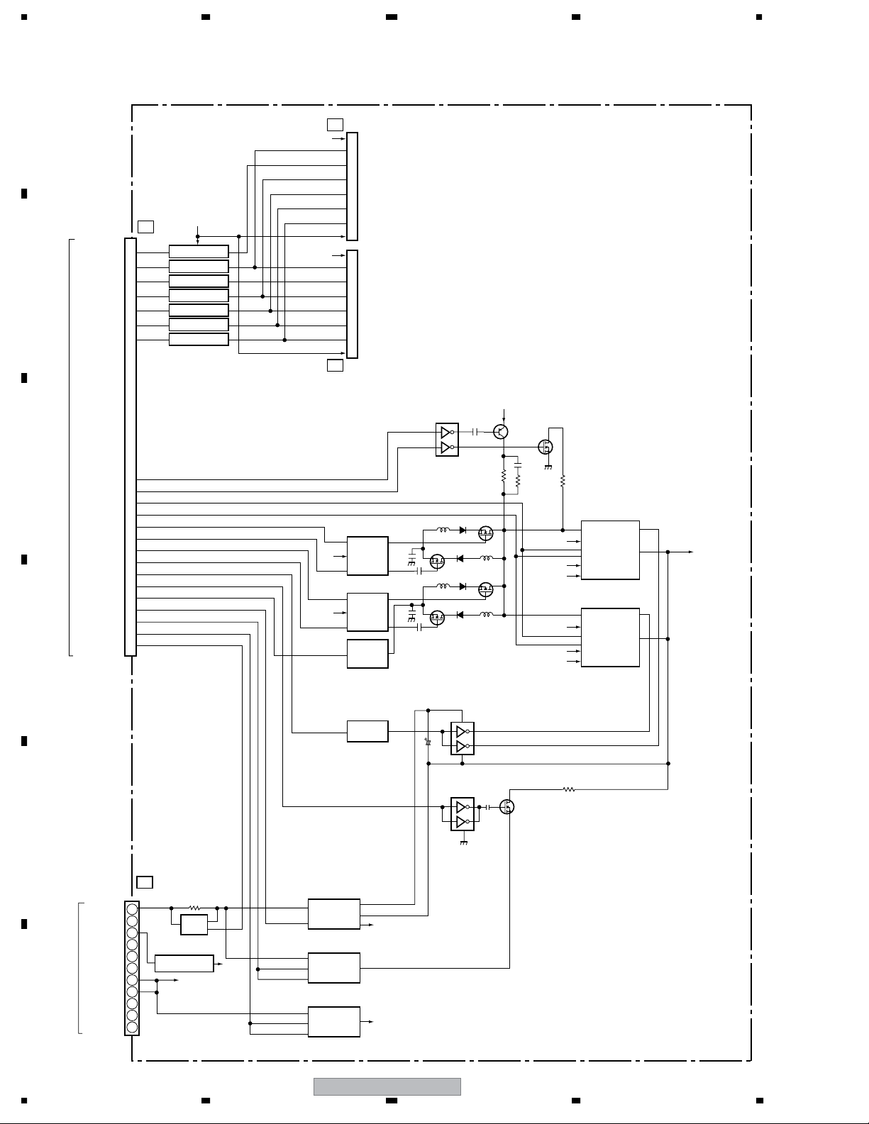
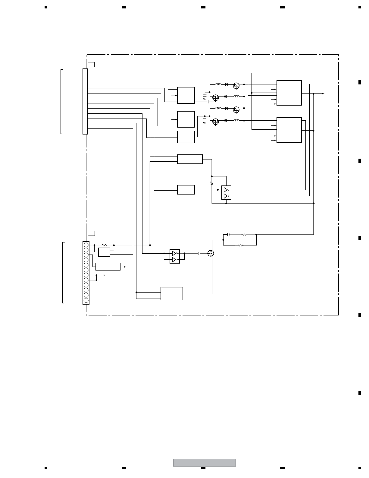
3.1.4 PANEL IF ASSY
• Block Diagram
A
PANEL IF ASSY
R3
TMDS
CN4003CN4002
6: DDC_SCL
7: DDC_SDA
B
C
DVI CONNECTOR
14: DDC_+5V
11: MTXD
2: MRXD
3: P_ST_B
10: MR_ST_B
7: REQ
8: STB3V
9: KEY_B
14: REM_B
MDR CONNECTOR
15: STB_MT
I2C BUFFER
R2
IC4006 BUF
IC4006 BUF
IC4006 BUF
IC4006 BUF
Q4004 INV
Q4006 INV
Q4006 INV
Q4009 INV
D
IC4202
TMDS RECEIVER
IC4206
Q4004
INV
Q4215
5V ↔ 3.3V
I2C LEVEL SHIFT
Q4007,
Q4011
NOR
Q4017
INV
IC4205
RESET IC
Q4006 INV
Q4006 INV
IC4002
BACKUP ROM
IC4006 BUF
IC4006 BUF
Q4011 INV
Q4001
5V ↔ 3.3V
I2C LEVEL SHIFT
R4
RSTBTMD
DVI_MUTE
DVI_OFF
RXD0
TXD0
B_SCL, B_SDA
CN4004CN4009
MR_ST_B
REQ_MD
MR_AC_OFF
KEY_B
REM_B
LED_R_B
LED_G_B
A_NG,A_MUTE,STB_SW,
FOCUS,TRUBASS,SRS
A_SCL, A_SDA
R7
13: AUDIO_R
20: AUDIO_L
R8
REM
CN4010
KEY
LED R
LED G
R_IN
L_IN
E
F
26
PDP-505PE
1234
Page 27
5678
• Voltages
CN4001 (R1) < ⇔ POWER SUPPLY UNIT >
No. Signal Name I/O Signal Description Voltages at NTSC Signal Input
1 6.5V I +6.5V power supply +6.8VDC
2 6.5V I +6.5V power supply +6.8VDC
3 Vcc_GND − GND
4 Vcc_GND − GND
5 STB3.3V I Power supply +3.3V input of module UCOM at panel side +3.3VDC
6 STB_GND − GND
7 STB3.3MUTE O Standby control (+3.3V mute) +3.3 VDC
8 AC_DET I Primary power supply (AC) state input at panel side +3.0VDC
CN4002 (R2) < ⇔ MEDIA RECEIVER >
No. Signal Name I/O Signal Description Voltages at NTSC Signal Input
1 MR_ST_B I
2 MRXD O
3 P_ST_B O
4 ACT3V O
5 AC_OFF O
6 GND
7 REQ O
8 STB3V I
9 KEY_B O
10 MR_ST_B' I
11 MTXD I
12 GND
13 AUDIO_R I
14 REM_B O
15 STB_MT I
16 GND
17 NC
18 FIELD I
19 GND
20 AUDIO_L I
Connection state detecting signal with MR
UART communication transmission data with the main UCOM (external PC)
at MR side
Connection state output for the MR
Power supply +3.3V output of module UCOM at panel side
Primary power supply (AC) state output at panel side
−
GND
Communication request to the main UCOM (external PC) at the MR
Standby power supply (+3.3V) input from the MR
Function key code signal output at panel side
Connection state detecting signal with the MR
UART communication receive data with the main UCOM (external PC) at
the MR side
−
GND
R ch audio signal input Audio R signal
Remote control code signal output
Standby control input
−
GND
−
Not connected
FIELD control signal
−
GND
L ch audio signal input Audio L signal
0VDC
0-3.3V amplitude square wave
0VDC
+3.3VDC
0VDC
0-3.3V amplitude square wave
+3.3VDC
0-3.3V amplitude square wave (at key
operation)
0VDC
0-3.3V amplitude square wave
0-3.3V amplitude square wave (at remocon
code transmission)
0VDC
−
0VDC
A
B
C
D
CN4003 (R3) < ⇔ MEDIA RECEIVER >
No. Signal Name I/O Signal Description Voltages at NTSC Signal Input
1 RX2- I
2 RX2+ I
3 GND
4 N.C
5 N.C
6 DDC_SCL I
7 DDC_SDA I
8 N.C
9 RX1- I
10 RX1+ I
11 GND
12 N.C
13 N.C
14 DDC_+5V I
15 GND
16 HPD O
17 RX0- I
18 RX0+ I
19 GND
20 N.C
21 N.C
56
DVI signal DVI differential signal (-)
DVI signal DVI differential signal (+)
−
GND
−
Not connected
−
Not connected
I2C signal for DDC
I2C signal for DDC 0-5V amplitude square wave
−
Not connected
DVI signal DVI differential signal (-)
DVI signal DVI differential signal (+)
−
GND
−
Not connected
−
Not connected
I2C power supply for DDC
−
GND
Hot plug detection
DVI signal DVI differential signal (-)
DVI signal DVI differential signal (+)
−
GND
−
Not connected
−
Not connected
−
−
0-5V amplitude square wave
−
−
−
+5VDC
+5VDC
−
−
PDP-505PE
7
8
E
F
27
Page 28
1234
• Voltages
CN4003 (R3) < ⇔ MEDIA RECEIVER >
A
No. Signal Name I/O Signal Description Voltages at NTSC Signal Input
22 GND
23 RXC+ I
24 RXC- I
CN4009 (R7) < ⇔ HD AUDIO AMP ASSY >
No. Signal Name I/O Signal Description Voltages at NTSC Signal Input
1 A_NG I
2 V+6.5 O
3 GNDA
4 L_IN O
B
5 GNDA
6 R_IN O
7 ST_BY O
8 A_MUTE O
9 SCL O
10 SDA O
11 FOCUS O
12 SRS O
13 TRUBASS O
−
GND
DVI signal DVI differential signal (-)
DVI signal DVI differential signal (+)
Abnormal detecting signal of the audio block
+6.5V power supply
−
GND
L ch audio signal Audio L signal
−
GND
R ch audio signal Audio R signal
Standby signal of the audio block +3.3V DC
Audio mute signal input 0V DC
I2C control signal for audio 0-3.3V amplitude square wave
I2C control signal for audio 0-3.3V amplitude square wave
Focus function control signal +3.3V DC
SRS function control signal +3.3V DC
TRUBASS function control signal +3.3V DC
+3.3V DC
+6.8V DC
CN4010 (R8) < ⇔ PANEL LED ASSY, PANEL IR ASSY, KEY CONTROL ASSY >
C
No. Signal Name I/O Signal Description Voltages at NTSC Signal Input
1 LED_G O
2 LED_R O
3 AC_OFF O
4 STB3V O
5 STBGND
6 REM I
7 STB+3V O
8 KEY I
9 STBGND
D
LED control (green)
LED control (red)
Primary power supply (AC) state output at the panel side
+3.3V power supply +3.3V DC
− GND
Remote control code signal input
+3.3V power supply +3.3V DC
Function key code signal input at the panel side
− GND
+2.1VDC
0VDC
0VDC
0-3.3V amplitude square wave (at remocon
code transmission)
0-3.3V amplitude square wave (at key operation)
CN4801 (SW1) < ⇔ KEY CONTROL ASSY >
No. Signal Name I/O Signal Description Voltages at NTSC Signal Input
1 STBGND
2G1 O
3G0 O
4D5 I
5D6 I
6D7 I
E
−
GND 0V DC
Key scan signal 0V DC
Key scan signal 0V DC
Key scan signal +3.3V DC
Key scan signal +3.3V DC
Key scan signal +3.3V DC
F
28
1234
PDP-505PE
Page 29

5678
• Voltages
CN4004 (R4) < ⇔ DIGITAL VIDEO ASSY > (1/2)
No. Signal Name I/O Signal Description Voltages at NTSC Signal Input
1 GND
2 GND
3
GND
GND
4
5 BA0 O
6 BA1 O
7 BA2 O
8 BA3 O
9 BA4 O
10 BA5 O
11 BA6 O
12 BA7 O
13 GND
14 GND
GND
15
GND
16
17 GA0 O
18 GA1 O
19 GA2 O
20 GA3 O
21 GA4 O
22 GA5 O
23 GA6 O
24 GA7 O
25 GND
26 GND
GND
27
GND
28
29 RA0 O
30 RA1 O
31 RA2 O
32 RA3 O
33 RA4 O
34 RA5 O
35 RA6 O
36 RA7 O
37
GND\
38 DCLK O
39 GND
40 DEI O
41 HDI O
42 VDI O
43 FIELD O
44 APL_DT
45
GND
GND
46
47 BB0 O
48 BB1 O
49 BB2 O
50 BB3 O
51 BB4 O
52 BB5 O
53 BB6 O
54 BB7 O
55 GND
56 GND
57
GND
GND
58
−
GND
−
GND
−
GND
−
GND
8bit video signal output (BLUE even number) 0-3.3V amplitude square wave
8bit video signal output (BLUE even number) 0-3.3V amplitude square wave
8bit video signal output (BLUE even number) 0-3.3V amplitude square wave
8bit video signal output (BLUE even number) 0-3.3V amplitude square wave
8bit video signal output (BLUE even number) 0-3.3V amplitude square wave
8bit video signal output (BLUE even number) 0-3.3V amplitude square wave
8bit video signal output (BLUE even number) 0-3.3V amplitude square wave
8bit video signal output (BLUE even number) 0-3.3V amplitude square wave
−
GND
−
GND
−
GND
−
GND
8bit video signal output (GREEN even number) 0-3.3V amplitude square wave
8bit video signal output (GREEN even number) 0-3.3V amplitude square wave
8bit video signal output (GREEN even number) 0-3.3V amplitude square wave
8bit video signal output (GREEN even number) 0-3.3V amplitude square wave
8bit video signal output (GREEN even number) 0-3.3V amplitude square wave
8bit video signal output (GREEN even number) 0-3.3V amplitude square wave
8bit video signal output (GREEN even number) 0-3.3V amplitude square wave
8bit video signal output (GREEN even number) 0-3.3V amplitude square wave
−
GND
−
GND
−
GND
−
GND
8bit video signal output (RED even number) 0-3.3V amplitude square wave
8bit video signal output (RED even number) 0-3.3V amplitude square wave
8bit video signal output (RED even number) 0-3.3V amplitude square wave
8bit video signal output (RED even number) 0-3.3V amplitude square wave
8bit video signal output (RED even number) 0-3.3V amplitude square wave
8bit video signal output (RED even number) 0-3.3V amplitude square wave
8bit video signal output (RED even number) 0-3.3V amplitude square wave
8bit video signal output (RED even number) 0-3.3V amplitude square wave
−
GND
Synchronous signal output (clock) 0-3.3V amplitude square wave (42.5MHz)
−
GND
Synchronous signal output (data enable)
Synchronous signal output (Horizontal sync.)
Synchronous signal output (Vertical sync.)
FIELD control signal 0V DC
Not connected
−
GND
−
GND
8bit video signal output (BLUE odd number) 0-3.3V amplitude square wave
8bit video signal output (BLUE odd number) 0-3.3V amplitude square wave
8bit video signal output (BLUE odd number) 0-3.3V amplitude square wave
8bit video signal output (BLUE odd number) 0-3.3V amplitude square wave
8bit video signal output (BLUE odd number) 0-3.3V amplitude square wave
8bit video signal output (BLUE odd number) 0-3.3V amplitude square wave
8bit video signal output (BLUE odd number) 0-3.3V amplitude square wave
8bit video signal output (BLUE odd number) 0-3.3V amplitude square wave
−
GND
−
GND
−
GND
−
GND
−
−
−
−
−
−
−
−
−
−
−
−
−
−
0-3.3V amplitude square wave (positive polarity)
0-3.3V amplitude square wave (negative polarity)
0-3.3V amplitude square wave (negative polarity)
−
−
−
−
−
−
−
A
B
C
D
E
F
56
PDP-505PE
29
7
8
Page 30
1234
• Voltages
CN4004 (R4) < ⇔ DIGITAL VIDEO ASSY > (2/2)
A
No. Signal Name I/O Signal Description Voltages at NTSC Signal Input
59 GB0 O
60 GB1 O
61 GB2 O
62 GB3 O
63 GB4 O
64 GB5 O
65 GB6 O
66 GB7 O
67 GND
68 GND
B
C
D
E
F
GND
69
70
GND
71 RB0 O
72 RB1 O
73 RB2 O
74 RB3 O
75 RB4 O
76 RB5 O
77 RB6 O
78 RB7 O
79 GND
80 MASK
81 MODE
82 MODEL
83 DITHER
84 V+3VACTV O Power supply +3.3V output of module UCOM at panel side +3.3VDC
85 B_SDA I E2PROM control signal for backup
86 RXD0 O
87 REM_B O Remote control code signal output
88 TXD0 I
89 KEY_B O Function key code signal output at panel side
90 REQ_MD I
91 LED_R_B I LED control (red) +3.3VDC
92 MR_AC_OFF O AC state output at MR side 0VDC
93 LED_G_B I LED control (green) 0VDC
94 POWER Not connected −
95 DVI_MUTE I DVI mute signal input 0VDC
96 MR_ST_B O Connection state detecting signal with MR 0VDC
97 A_MUTE I Audio mute signal input 0VDC
98 OP_DET
99 A_NG O Abnormal detecting signal of audio block +3.3VDC
100 PNL_MUTE Not connected −
101 A_SCL I I2C control signal for audio
102 STB_SW I Standby signal of audio block +3.3VDC
103 A_SDA I I2C control signal for audio
104 DDC_WP I
105 TRUBASS I TRUBASS function control signal +3.3VDC
106 B_SCL I E2PROM control signal for backup
107 FOCUS I FOCUS function control signal +3.3VDC
108 DVI_OFF O Connection detecting signal of DVI connector 0VDC
109 SRS I SRS function control signal +3.3VDC
110 RSTBTMD O TMDS IC reset signal +3.3VDC
111 MAX_PLS1 Not connected −
112 L_SYNC O TMDS IC synchronous detecting signal +3.3VDC
113 MAX_PLS2 Not connected −
114 GND
8bit video signal output (GREEN odd number) 0-3.3V amplitude square wave
8bit video signal output (GREEN odd number) 0-3.3V amplitude square wave
8bit video signal output (GREEN odd number) 0-3.3V amplitude square wave
8bit video signal output (GREEN odd number) 0-3.3V amplitude square wave
8bit video signal output (GREEN odd number) 0-3.3V amplitude square wave
8bit video signal output (GREEN odd number) 0-3.3V amplitude square wave
8bit video signal output (GREEN odd number) 0-3.3V amplitude square wave
8bit video signal output (GREEN odd number) 0-3.3V amplitude square wave
−
GND
−
GND
−
GND
−
GND
8bit video signal output (RED odd number) 0-3.3V amplitude square wave
8bit video signal output (RED odd number) 0-3.3V amplitude square wave
8bit video signal output (RED odd number) 0-3.3V amplitude square wave
8bit video signal output (RED odd number) 0-3.3V amplitude square wave
8bit video signal output (RED odd number) 0-3.3V amplitude square wave
8bit video signal output (RED odd number) 0-3.3V amplitude square wave
8bit video signal output (RED odd number) 0-3.3V amplitude square wave
8bit video signal output (RED odd number) 0-3.3V amplitude square wave
−
GND
Not connected
Not connected
Not connected
Not connected
UART communication receive data with the main UCOM (external PC) at MR side
UART communication transmission data with the main UCOM (external PC) at MR side
Communication request to the main UCOM at MR side
GND
GND
−
GND
−
−
−
−
0-3.3V amplitude square wave
0-3.3V amplitude square wave
0-3.3V amplitude square wave (at remocon
code transmission)
0-3.3V amplitude square wave
0-3.3V amplitude square wave (at key
operation)
0-3.3V amplitude square wave
0-3.3V amplitude square wave
0-3.3V amplitude square wave
0-3.3V amplitude square wave
30
PDP-505PE
1234
Page 31

5678
LVDS
(R,G,B) x10bit x2
YSUSA,YSUSB
SCAN
Works by passive standby power
Works by active standby power
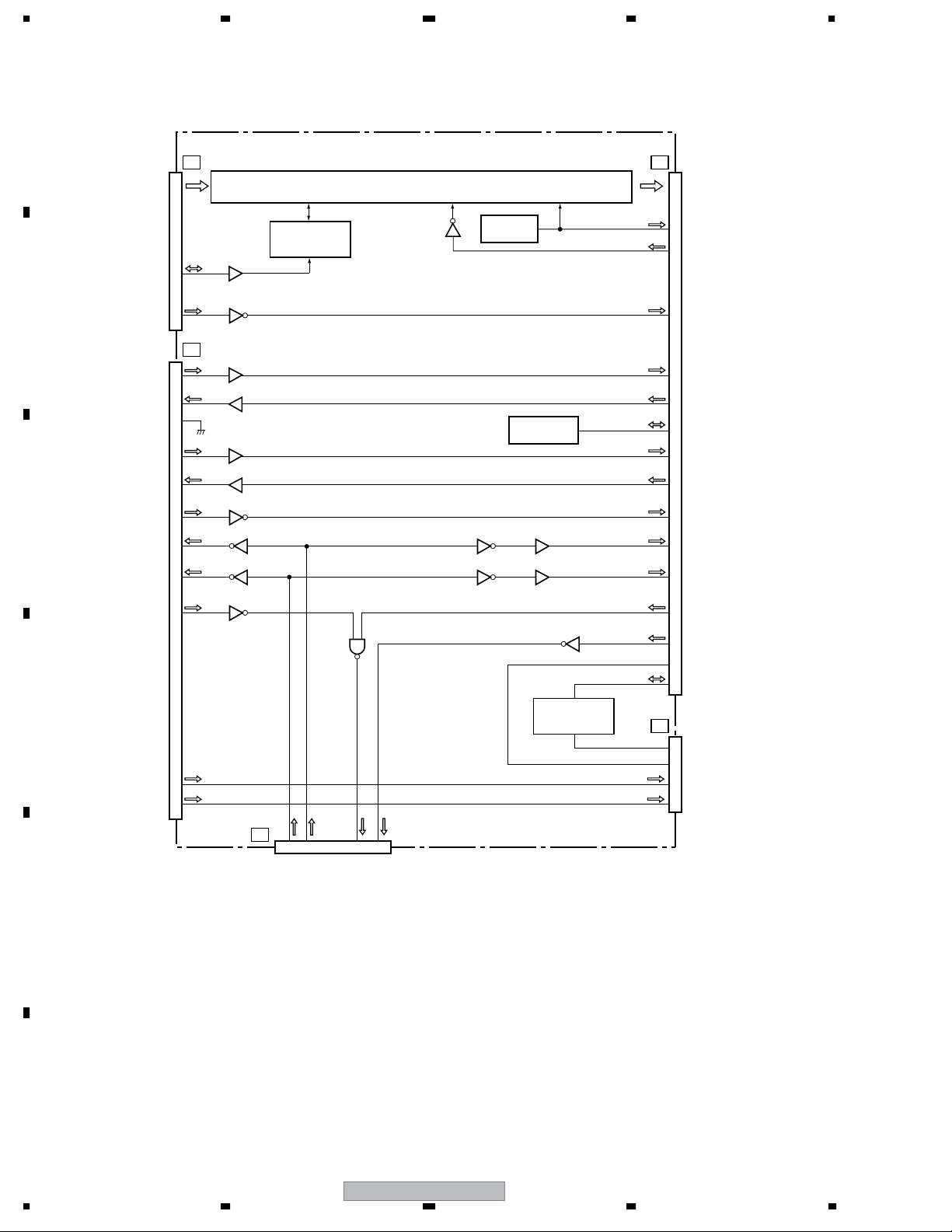
3.1.5 DIGITAL VIDEO ASSY
• Block Diagram
CN5001
From PANEL IF ASSY
Works by passive standby power
Works by passive standby power Works by active standby power
DIGITAL VIDEO ASSY
(R,G,B) x10bit x2
(R,G,B) x10bit x2
HD, VD, CLK, DE
OR
OR
1.5V
3.3V
RST
RST
IC
IC
For HD model
3 STATE3STATE
3STATE
For panel module
Xtal
RST2
IC4_RST
DVI_DET
MSTATE
RSTBTMDS
L_SYNC
VD_IN
DVI_MUTE
OP_DET
WE_IC4
A_SCL/A_SDA
Excepting panel module
RXD0
TXD0
REQ
CST3
MODEL
B_SCL/B_SDA
MRAC_DET
MODE
KEY
REM
POWER
PNL_MUTE
DITHER
MAX_PLS1
MAX_PLS2
MASK1
STB_SW
SRS
FOCUS
TRUBASS
A_MUTE
LED_R
LED_G
AC_DET
THEATER
MANTA
RST
TXD
CLK
IC4_CE
MODULE UC OM
IC5201
DRIVE_OFF
IC4
Works by active standby power
LVDS
LVDS
YSUSA,YSUSB
YSUSA,YSUSB
YSUSA, YSUSB
SCAN
SCAN
SCAN
XSUSA, XSUSB
FLASH
Sequence data
TCKTMS
TRST TDI
TDO
MUTE
RXD
IC4_BUSY
REQ_IC4
PD_TRG
EEPRST
ADR_PD
SCAN_PD
YDRV_PD
YRES_PD
YDC_PD
IC5V_PD
XSUS_PD
XDC_PD
XDRV_PD
PS_PD
DCC_PD
YDRV_UC
XDRV_UC
PD_MUTE
PSIZE
PSW_D
RESET
TEMP1
E_SCL
E_SDA
DC- DC
CONV.
BUSY
RXD1
CLK1
CNVSS
TXD1
VOFS
VSUS
RELAY
ROM
ROM
EEP
Xtal
JTAG
FLASH
writing
&
Writing
AND
3.3V
RST
50 ADDRESS ASSY x8
IC5
PANEL
SIZE
OR
50 Y DRIVE
ASSY
PD
SCAN
ASSY
Video signal
Sync. signal
3-wire serial down
3-wires serial up
Signal for JTAG
Parallel bus
IIC communication
Asynchronous serial down
Asynchronous serial up
Others
A
B
MUTE
PD
PD
PD
PD
PD
Connector
disconnection
detection
Vofs
50 X DRIVE
ASSY
C
MUTE
PD
PD
PD
OR
D
Connector
disconnection
PD
MUTE
OR
8bit
DAC
IC
detection
Vrst
Vm adj: STB
PANEL SENSOR ASSY
Terrmal
sensor
E
CN4001
POWER SUPPLY ASSY
ASSY
From PANEL IF
Mechanism
SW for Mute
RELAY CONTROL
POWER ON
RELAY
STB_MT
STB3.3V
AC_DET
AC- OFF
DRIVE
OF
PD
LED
F
PDP-505PE
56
Vsus
Each
OR
PD
31
F
7
8
Page 32

1234
• Voltages
CN5601 (D1)
A
No. Signal Name I/O Signal Description Voltages at NTSC Signal Input
1 +12V I
2 +12V I
3 GND_D
4 GND_D
5PD O
6 VSUS_ADJ O
7 PS_PD I
8 RELAY O
9 DRF O
10 AC_DET I
B
11 PD_TRIGGER I
CN5602 (D2)
No. Signal Name I/O Signal Description Voltages at NTSC Signal Input
1 VADR I
2 VADR I
3 N.C
4 GND_ADR
5 GND_ADR
C
6 +6.5V I
7 GND_D
+12V power input
+12V power input
GND
−
GND
−
Power down signal
VSUS adjustment signal
Power-down detecting signal of POWER SUPPLY block
Relay control signal
Drive control signal
Primary side power (AC) state output at panel side
Power down trigger
Address drive power (+61V) input
Address drive power (+61V) input
Not connected
GND
−
GND
−
+6.5V power input
GND
−
+12VDC
+12VDC
0VDC
0VDC
+3.3VDC
0VDC
+3.0VDC
+3.3VDC
+61VDC
+61VDC
+6.8VDC
D
E
F
32
PDP-505PE
1234
Page 33

5678
3.1.6 HD AUDIO AMP ASSY
A1
+6.5V
R_Audio
L_Audio
SCL, SDA
SRS,FOCUS,TRUBASS
HD AUDIO AMP ASSY
+9.0V +9.0V
WOW IC
IC3501
+9.0V
From POWER SUPPLY Unit
+16.5V
VOLUME IC
IC3502
BUFFER
A
CN3504
A2
B
From PANEL IF ASSY
A_Mute
ST-BY
A_NG_B
+16.5V
CN3501
REGULATOR
IC3503
DC DETECT
BLOCK
CN3503
POWER AMP
IC3504
+
R_OUT+
R_OUT-
L_OUT -
L_OUT
J3701
HD SP TERMINAL ASSY
L OUTR OUT
A3
SP2
+16.5V
IC
SP1
C
D
E
56
PDP-505PE
F
33
7
8
Page 34

1234
3.2 WAVEFORMS
DIGITAL VIDEO ASSY (4/6)
A
• DIGITAL IF BLOCK
CH1: TP5102 (VD)
1
CH2: TP5101 (HD)
V: 2V/div. H: 2msec/div.
CH1: TP5101 (HD)
3
CH2: TP5103 (DE)
V: 2V/div. H: 2µsec/div.
CH1
CH2
B
CH1: TP5102 (VD)
1
CH2: TP5101 (HD)
V: 2V/div. H: 4µsec/div.
CH1
CH2
C
CH1: TP5102 (VD)
2
CH2: TP5103 (DE)
V: 2V/div. H: 2msec/div.
CH1
CH1
CH2
CH1: TP5101 (HD)
3
CH2: TP5103 (DE)
V: 2V/div. H: 40nsec/div.
CH1
CH2
CH1: TP5101 (HD)
4
CH2: CN5001-pin 77 (DCLK)
V: 2V/div. H: 40nsec/div.
CH1
CH2
D
CH1: TP5102 (VD)
2
CH2: TP5103 (DE)
V: 2V/div. H: 4µsec/div.
CH1
CH2
E
F
CH2
CH1: TP5102 (VD)
5
CH2: CN5001-pin 86 (RA_IN2)
V: 2V/div. H: 2msec/div.
CH1
CH2
34
PDP-505PE
1234
Page 35

5678
PANEL IF ASSY (1/2)
• TMDS RX BLOCK
CH1: K4005 (VDI)
1
CH2: K4006 (HDI)
V: 2V/div. H: 5msec/div.
CH1
CH2
CH1: K4005 (VDI)
1
CH2: K4006 (HDI)
V: 2V/div. H: 10µsec/div.
CH1
CH2
CH1: K4006 (HDI)
3
CH2: K4003 (DEI)
V: 2V/div. H: 5µsec/div.
CH1
CH2
CH1: K4003 (DEI)
4
CH2: K4002 (DCLK)
V: 2V/div. H: 5µsec/div.
CH1
CH2
A
B
C
CH1: K4005 (VDI)
2
CH2: CN4004-pin 29 (RAO)
V: 2V/div. H: 5msec/div.
CH1
CH2
CH1: K4003 (DEI)
4
CH2: K4002 (DCLK)
V: 2V/div. H: 10nsec/div.
CH1
CH2
D
E
56
PDP-505PE
F
35
7
8
Page 36

1234
50 X DRIVE ASSY, 50 Y DRIVE ASSY and 50 SCAN A ASSY
A
• 50 X SUS BLOCK, 50 Y LOGIC BLOCK, 50 Y SUS BLOCK
1
Drive Output Waveform (1 field,color-bar)
CH1: R1226 (XPSUS) - K1201 (SUSGND)
(50 X DRIVE ASSY)
CH2: R2348 (YPSUS) - K2301 (SUSGND)
(50 Y DRIVE ASSY)
CH3: K3001 (Scan OUT) - K2301 (SUSGND)
(50 SCAN A ASSY)
V: 100V/div. H: 2msec/div.
CH1
B
CH2
CH3
3
Control Signal (Sustain Waveform Gen.)
CH2: K2016 (YSUS-G) - K2010 (DGND)
CH3: K2025 (YSUS-U1) - K2010 (DGND)
CH4: K2022 (YSUS-U2) - K2010 (DGND)
CH5: K2026 (YSUS-B) - K2010 (DGND)
CH6: K2024 (YSUS-D2) - K2010 (DGND)
CH7: K2027 (YSUS-D1) - K2010 (DGND)
(50 Y DRIVE ASSY)
V: 1V/div. H: 500nsec/div.
CH2
CH3
CH4
CH5
CH6
CH7
Reset Pulse
1
CH1: R1226 (XPSUS) - K1201 (SUSGND)
(50 X DRIVE ASSY)
CH2: R2348 (YPSUS) - K2301 (SUSGND)
(50 Y DRIVE ASSY)
CH3: K3001 (Scan OUT) - K2301 (SUSGND)
(50 SCAN A ASSY)
V: 100V/div. H: 100µsec/div.
C
CH1
CH2
CH3
Sustain Pulse (1 sub-sub-field)
1
CH1: R1226 (XPSUS) - K1201 (SUSGND)
(50 X DRIVE ASSY)
CH2: R2348 (YPSUS) - K2301 (SUSGND)
(50 Y DRIVE ASSY)
D
CH3: K3001 (Scan OUT) - K2301 (SUSGND)
(50 SCAN A ASSY)
V: 50V/div. H: 5µsec/div.
Scan Control Signal (1 field, color-bar)
4
CH2: K2006 (SI) - K2029 (DGND)
CH3: K2009 (OC1) - K2029 (DGND)
CH4: K2004 (OC2) - K2029 (DGND)
CH5: K2007 (CLR) - K2029 (DGND)
CH6: K2003 (CLK2) - K2029 (DGND)
CH7: K2008 (LE) - K2029 (DGND)
(50 Y DRIVE ASSY)
V: 1V/div. H: 2msec/div.
CH2
CH3
CH4
CH5
CH6
CH7
X Drive Pulse Control Signal (color-bar)
5
CH1: R1226 (XPSUS) - K2301 (SUSGND)
V: 100V/div. H: 2msec/div.
CH2: K1016 (XCP-MSK) - K1020 (DGND)
CH3: K1015 (XSUS-MSK) - K1020 (DGND)
CH4: K1014 (XNR-D) - K1020 (DGND)
V: 1V/div. H: 2msec/div.
(50 X DRIVE ASSY)
CH1
CH1
CH2
CH2
CH3
CH3
CH4
Sustain Waveform
E
2
CH1: R2348 (YPSUS) - K2301 (SUSGND)
(50 Y DRIVE ASSY)
V: 50V/div. H: 500nsec/div.
Y Drive Pulse Control Signal (color-bar)
6
CH1: R2348 (YPSUS) - K2301 (SUSGND)
V: 50V/div. H: 2msec/div.
CH2: K2015 (YSUS-MSK) - K2010 (DGND)
CH3: K2017 (YSOFT-D) - K2010 (DGND)
CH4: K2023 (YPR-U) - K2010 (DGND)
V: 1V/div. H: 2msec/div.
(50 Y DRIVE ASSY)
CH1
CH1
CH2
CH3
F
36
PDP-505PE
CH4
1234
Page 37

5678
50 ADDRESS ASSY
• ADR RESONANCE BLOCK (VIDEO and PC)
CH1: IC1601-pin 2 (ADR_B2)
1
CH2: IC1603-pin 4 (ADR_U1)
CH3: IC1603-pin 2 (ADR_D1)
V: 1V/div.
(Input: VIDEO, Signal: Color-bar)
CH1
CH2
CH3
CH1
CH2
CH3
CH1: IC1601-pin 2 (ADR_B2)
2
CH2: IC1602-pin 4 (ADR_U2)
CH3: IC1602-pin 2 (ADR_D2)
V: 1V/div.
(Input: VIDEO, Signal: Color-bar)
CH1
CH2
CH3
CH1
CH2
CH3
H:
2msec/div.
H:
1µsec/div.
H:
2msec/div.
H:
1µsec/div.
3
CH2
CH3
CH4
CH2
CH3
CH4
4
CH2
CH3
CH4
CH2
CH3
CH4
CH2: Q1601-pin 4 (ADR_B2)
CH3: Q1603-pin 4 (ADR_U1)
CH4: Q1603-pin 2 (ADR_D1)
V: 10V/div.
(Input: VIDEO, Signal: Color-bar)
CH2: Q1601-pin 4 (ADR_B2)
CH3: Q1602-pin 4 (ADR_U2)
CH4: Q1602-pin 2 (ADR_D2)
V: 10V/div.
(Input: VIDEO, Signal: Color-bar)
H:
1µsec/div.
H:
1µsec/div.
H:
1µsec/div.
H:
1µsec/div.
CH1: Q1601 Drain (V+ADR)
5
CH2: Q1603 Source
CH3: Q1602 Source
V: 10V/div.
(Input: VIDEO, Signal: Color-bar)
CH1
CH2
CH3
CH1
CH2
CH3
CH1: Q1601 Drain (V+ADR)
6
CH2: Q1603 Source
CH3: Q1602 Source
V: 10V/div.
(Input: VIDEO, Signal: B/W(1×8))
CH1
CH2
CH3
CH1
CH2
CH3
H:
2msec/div.
H:
1µsec/div.
H:
2msec/div.
H:
1µsec/div.
A
B
C
50 ADDRESS ASSY
• ADR LOGIC BLOCK
CH1: IC1553-pin 18 (CLK input)
1
CH2: IC1553-pin 16 (LE input)
CH3: IC1553-pin 9 (DATA input)
V: 1V/div.
(Input: VIDEO, Signal: Color-bar)
CH1
CH2
CH3
CH1
CH2
CH3
CH1: IC1553-pin 23 (HBLK input)
2
CH2: IC1553-pin 19 (LBLK input)
CH3: IC1553-pin 25 (HZ input)
V: 1V/div.
(Input: VIDEO, Signal: Color-bar)
CH1
CH2
CH3
CH1
CH2
CH3
H:
2msec/div.
H:
200nsec/div.
H:
2msec/div.
H:
50µsec/div.
D
E
56
PDP-505PE
F
37
7
8
Page 38

1234
5. PCB PARTS LIST
NOTES:
A
Parts marked by "NSP" are generally unavailable because they are not in our Master Spare Parts List.
The mark found on some component parts indicates the importance of the safety factor of the part.
Therefore, when replacing, be sure to use parts of identical designation.
When ordering resistors, first convert resistance values into code form as shown in the following examples.
Ex.1 When there are 2 effective digits (any digit apart from 0), such as 560 ohm and 47k ohm (tolerance is shown by J=5%,
and K=10%).
560 Ω
47k Ω
0.5 Ω
1 Ω
56 x 10
47 x 10
R50
1R0
Ex.2 When there are 3 effective digits (such as in high precision metal film resistors).
5.62k Ω
Mark No. Description Part No.
B
LIST OF ASSEMBLIES
NSP 1..50 ADDRESS ASSY AWV2080
NSP 2..50 ADDRESS ASSY AWZ6870
NSP 1..50 SCAN ASSY AWV2083
NSP 2..50 SCAN A ASSY AWZ6878
NSP 2..50 SCAN B ASSY AWZ6879
NSP 2..X CONNECTOR A ASSY AWZ6880
NSP 2..X CONNECTOR B ASSY AWZ6881
NSP 1..HD PANEL IF ASSY AWV2073
C
2..PANEL IF ASSY AWZ6841
1..DIGITAL VIDEO ASSY AWV2074
NSP 1..HD AUDIO ASSY AWV2075
2..HD AUDIO AMP ASSY AWZ6863
2..HD SP TERMINAL ASSY AWZ6864
NSP 1..50 X DRIVE ASSY AWV2081
2..PANEL LED ASSY AWZ6842
2..PANEL KEY ASSY AWZ6843
2..KEY CONTROL ASSY AWZ6844
2..PANEL IR ASSY AWZ6845
D
2..PANEL SENSOR ASSY AWZ6872
2..50 X DRIVE ASSY AWZ6877
1..50 Y DRIVE ASSY AWV2082
1..POWER SUPPLY UNIT AXY1085
E
F
38
1234
1
3
561
473
RD1/4PU J
RD1/4PU J
RN2H K
RS1P K
1
5621
RN1/4PC F562 x 10
561
473
R50
1R0
5621
Mark No. Description Part No.
50 ADDRESS ASSY
[50 ADR LOGIC BLOCK]
SEMICONDUCTORS
IC1501 PEE001B
COILS AND FILTERS
L1504 QTL1013
CAPACITORS
C1501, C1502 (47/6.3V) ACH1357
C1509, C1510 CKSSYB102K50
C1503-C1507, C1511, C1512, C1552 CKSSYF104Z16
C1555, C1558, C1561, C1564 CKSSYF104Z16
RESISTORS
R1510, R1519, R1522, R1526 RAB4C470J
R1505-R1509, R1530, R1531 RS1/16SS1000F
R1511-R1518, R1520, R1521, R1523 RS1/16SS470J
R1524, R1527, R1528, R1532-R1535 RS1/16SS470J
Other Resistors RS1/16S###J
OTHERS
CN1501 40P FFC CONNECTOR AKM1215
[50 ADR RESONANCE BLOCK]
SEMICONDUCTORS
IC1601-IC1603 TND307TD
Q1604 2SA1163
Q1601 HAT1110R
Q1602, Q1603 HAT3021R
D1601 1SS302
D1605, D1606, D1616, D1617 D1FL20U(S)
D1610, D1619 RF051UA1D
D1602, D1607, D1615 UDZS15(B)
COILS AND FILTERS
L1601, L1602 ATH1164
CAPACITORS
C1605 (0.01/100V) ACG1101
C1619, C1620 (330P/100V) ACG1105
C1609, C1615 (0.1/100V) ACG1119
C1618 (47/6.3V) ACH1357
C1603 (47/16V) ACH1391
C1601, C1602 (56/80V) ACH1405
C1608, C1614 CKSRYB104K25
C1604, C1606, C1612 CKSSYF104Z16
RESISTORS
R1631 ACN1174
PDP-505PE
>
Page 39

5678
Mark No. Description Part No.
Other Resistors RS1/16S###J
50 SCAN A ASSY
SEMICONDUCTORS
IC3001-IC3006 AN16021AA
D3003-D3006 1SS355
CAPACITORS
C3001, C3002, C3012, C3013 (0.1/250V)ACG1088
C3023, C3024, C3034, C3035 (0.1/250V)ACG1088
C3045, C3046, C3056, C3057 (0.1/250V)ACG1088
C3005, C3008, C3016, C3019, C3026 CCSRCH101J50
C3029, C3037, C3040, C3048, C3051 CCSRCH101J50
Mark No. Description Part No.
Other Resistors RS1/16S###J
OTHERS
CN3201 13P CONNECTOR NONPB AKP1261
K3203, K3208, K3214, K3216, K3218 AKX9002
K3221 TEST PIN AKX9002
X CONNECTOR A ASSY
This assembly has no service part.
A
C3060, C3063 CCSRCH101J50
C3007, C3018, C3033, C3044, C3050 CCSRCH181J50
C3062 CCSRCH181J50
C3006, C3011, C3017, C3022 CCSRCH331J50
C3031, C3032, C3042, C3043, C3049 CCSRCH331J50
C3055, C3061, C3066 CCSRCH331J50
C3009, C3010, C3020, C3021, C3028 CCSRCH390J50
C3030, C3039, C3041, C3053, C3054 CCSRCH390J50
C3064, C3065 CCSRCH390J50
C3003, C3014, C3025, C3036, C3047 CKSRYB105K6R3
C3058 CKSRYB105K6R3
RESISTORS
R3003, R3011, R3017, R3025, R3030 RAB4C221J
R3036 RAB4C221J
Other Resistors RS1/16S###J
OTHERS
CN3001 13P CONNECTOR NON PB AKP1261
K3001, K3004, K3009, K3015, K3017 AKX9002
K3019, K3021 TEST PIN AKX9002
50 SCAN B ASSY
SEMICONDUCTORS
IC3201-IC3206 AN16021AA
D3203-D3206 1SS355
CAPACITORS
C3201, C3211, C3212, C3222, C3223 ACG1088
C3233, C3234, C3244, C3245(0.1/250V)ACG1088
C3255, C3256, C3266 (0.1/250V) ACG1088
C3203, C3204, C3214, C3215, C3226 CCSRCH101J50
C3228, C3237, C3239, C3247, C3251 CCSRCH101J50
C3258, C3259 CCSRCH101J50
C3206, C3217, C3232, C3243, C3249 CCSRCH181J50
C3261 CCSRCH181J50
C3205, C3210, C3216, C3221 CCSRCH331J50
C3230, C3231, C3241, C3242, C3248 CCSRCH331J50
C3254, C3260, C3265 CCSRCH331J50
C3208, C3209, C3219, C3220, C3227 CCSRCH390J50
C3229, C3238, C3240, C3252, C3253 CCSRCH390J50
C3263, C3264 CCSRCH390J50
C3202, C3213, C3224, C3235, C3246 CKSRYB105K6R3
X CONNECTOR B ASSY
This assembly has no service part.
PANEL IF ASSY
[PANEL IF BLOCK]
SEMICONDUCTORS
IC4002 BR24L02FJ-W
>
IC4003 NCP1117DT33
IC4006 SN74AHC541PW
Q4007 DTA143EUA
Q4004, Q4008, Q4009, Q4012 DTC143EUA
Q4014-Q4017 DTC143EUA
Q4005, Q4006, Q4010, Q4013 RN1901
Q4011 RN2901
Q4001 SM6K2
D4006 1SS355
D4001-D4004, D4007 RB751V-40
>
D4005 UDZS5R1(B)
COILS AND FILTERS
F4002 ATF1213
L4001 LCTAW221J3225
CAPACITORS
C4009, C4020 CCSRCH471J50
C4005, C4006 CCSSCH100D50
C4019 CCSSCH101J50
C4011, C4018, C4021 CEAT101M10
C4003, C4015 CEAT101M16
C4004, C4010, C4012, C4014 CKSRYB103K50
C4016, C4024, C4041 CKSSYF104Z16
RESISTORS
R4006 RAB4C101J
R4001 RS1/16S331J
Other Resistors RS1/16SS###J
OTHERS
CN4004 114PFFC CONNECTOR AKM1216
CN4003 DVI SOCKET (24P) AKP1216
CN4002 SOCKET (20P) AKP1226
CN4001 PLUG (8P) KM200NA8
CN4010 PLUG (9P) KM200NA9
CN4009 PLUG (13P) KM200NA13
B
C
D
E
C3257 CKSRYB105K6R3
RESISTORS
R3202, R3210, R3216, R3224, R3229 RAB4C221J
R3235 RAB4C221J
56
[TMDS RX BLOCK]
SEMICONDUCTORS
PDP-505PE
IC4206 BA8274F
IC4205 PST3628UR
IC4202 SII169CTG100
7
8
F
39
Page 40

1234
Mark No. Description Part No.
Q4215 SM6K2
D4203, D4204 1SS355
D4202 UDZS6R8(B)
A
COILS AND FILTERS
L4201 ATH1162
CAPACITORS
C4208, C4215, C4218, C4222, C4230 CCSRCH331J50
C4262 CCSRCH471J50
C4207, C4210, C4232, C4233, C4236 CCSSCH820J50
C4241, C4244, C4258 CCSSCH820J50
C4242, C4246 CEAT101M10
C4202, C4237, C4238 CEAT470M10
C4260 CKSRYB472K50
B
C4203, C4213, C4240, C4243, C4247 CKSSYF104Z16
C4261, C4271 CKSSYF104Z16
RESISTORS
R4241 RAB4C220J
R4213-R4218, R4245, R4247 RAB4C470J
R4253-R4255, R4257 RAB4C470J
R4250 RS1/16S3900F
R4222- R4225 RS1/16S0R0J
Mark No. Description Part No.
RESISTORS
R5209, R5211, R5212, R5235 RAB4C101J
R5254, R5255, R5265, R5266 RAB4C101J
R5205 RAB4C103J
R5270, R5271 RAB4C472J
R5256, R5257 RAB4C474J
R5294 RS1/16S0R0J
Other Resistors RS1/16SS###J
OTHERS
CN5201 PLUG 8-P AKM1225
CN5202 CONNECTOR AKM1274
>
X5201 CERAMIC RESONATOR ASS1178
[PANEL FLASH BLOCK]
SEMICONDUCTORS
IC5305 MBM29PL160BD-75PFTN
IC5303 PST3612UR
IC5301 PST3628UR
IC5302 SN74AHC08PW
Q5301 RN1901
Other Resistors RS1/16SS###J
C
DIGITAL VIDEO ASSY
[DIGITAL IF BLOCK]
RESISTORS
R5101-R5115, R5131 RAB4C470J
Other Resistors RS1/16SS###J
OTHERS
CN5001 114P FFC CONNECTOR AKM1216
[MODULE UCOM BLOCK]
D
SEMICONDUCTORS
IC5206 BR24L04FJ-W
IC5201 M30622F8PGP
IC5205 PST3628UR
IC5208 SN74AHC08PW
IC5214, IC5215 SN74AHC32PW
IC5211, IC5212 SN74AHC541PW
IC5209 TC7W126FU
Q5201 2SJ461A
Q5202 DTC143EUA
D5217 1SS355
E
D5207-D5212 DAN202U
D5201 SML-310LT
D5301-D5310 DA204U
CAPACITORS
C5320 CCSRCH470J50
C5321, C5322 CCSRCH471J50
C5311, C5314 CKSRYB104K16
C5303, C5306 CKSRYB472K50
C5304, C5307 CKSSYB102K50
C5301, C5302, C5305, C5309, C5313 CKSSYF104Z16
C5316 CKSSYF104Z16
RESISTORS
R5317, R5318 RAB4C101J
Other Resistors RS1/16SS###J
OTHERS
CN5301 PLUG 15-P AKM1232
>
X5302 CRYSTAL OSCILLATOR ASS1174
>
X5301 CRYSTAL OSCILLATOR ASS1182
[IC4 BLOCK]
SEMICONDUCTORS
IC5401 PEG054A
D5401 SML-310LT
D5402 SML-310MT
COILS AND FILTERS
F5401, F5403, F5409, F5410 ATF1213
SWITCHES AND RELAYS
S5201 ASH1047
CAPACITORS
C5213, C5225 ACH1357
C5205 CKSRYB472K50
C5206, C5223, C5231, C5245-C5252 CKSSYB102K50
C5257- C5260 CKSSYB102K50
C5202-C5204, C5207, C5208 CKSSYF104Z16
F
C5210-C5212, C5218, C5224 CKSSYF104Z16
C5226, C5227, C5243, C5244 CKSSYF104Z16
40
1234
CAPACITORS
C5401, C5413, C5417, C5424 ACH1396
(100UF/6.3V)
C5434, C5435 CKSSYB102K50
C5402-C5412, C5414-C5416 CKSSYF104Z16
C5418-C5423, C5425-C5431 CKSSYF104Z16
RESISTORS
R5406, R5421 RAB4C101J
R5408-R5413, R5415, R5416, R5419 RAB4C220J
R5422 RAB4C220J
R5405 RS1/16S5601F
PDP-505PE
Page 41

5678
Mark No. Description Part No.
R5401-R5404 RS1/16S0R0J
Other Resistors RS1/16SS###J
Mark No. Description Part No.
C3559, C3560 CEHAT2R2M50
C3509 CEHAT331M16
C3507 CEHAT471M25
C3571 CEHAT472M25
C3563 CEHATR47M50
A
[ADDRESS CN BLOCK]
RESISTORS
Other Resistors RS1/16SS###J
OTHERS
CN5521 50P CONNECTOR AKM1201
>
CN5501-CN5508 40P CONNECTOR AKM1217
CN5511 30P FFC CONNECTOR AKM1218
[DIGITAL DD CON BLOCK]
SEMICONDUCTORS
>
IC5605 BA90BC0FP
>
IC5604 MM1665AT
Q5601 HN1C01FU
D5602, D5609 DAN202U
D5601 HZU2R2(B)
D5604 UDZS5R1(B)
CAPACITORS
C5601, C5603, C5614, C5616 ACH1394
(100UF/16V)
C5602, C5604, C5615, C5617 CKSRYB103K50
C5605, C5606 CKSSYF104Z16
RESISTORS
R5613 RS1/16S0R0J
Other Resistors RS1/16SS###J
OTHERS
>
CN5602 7P CONNECTOR AKM1278
>
CN5601 11P CONNECTOR AKM1282
U5602 DD CON UNIT AXY1086
HD AUDIO AMP ASSY
SEMICONDUCTORS
IC3502 BD3869AS
IC3504 LA4625
IC3501 NJM2195L
IC3503 NJM7809FA
Q3501, Q3502, Q3507, Q3510, Q3511 2SA1162
C3512, C3522, C3572 CFTLA103J50
C3511, C3513-C3518, C3533, C3534 CFTLA104J50
C3545-C3548, C3573-C3576 CFTLA104J50
C3521 CFTLA333J50
C3524 CFTLA334J50
C3523 CFTLA474J50
C3506, C3508, C3510, C3527, C3535 CKSRYB103K50
C3550, C3558 CKSRYB103K50
C3543, C3544 CQMA222J50
RESISTORS
R3599-R3602 RD1/2MMF2R2J
Other Resistors RS1/16S###J
OTHERS
3511 AUDIO HEATSINK ANH1612
CN3504 CONNECTOR B3P-VH
CN3502, CN3503 PLUG (6P) KM200NA6
CN3501 PLUG (13P) KM200NA13
3512-3515 SCREW VBB30P100FNI
KN3501, KN3502 VNF1084
WRAPPING TERMINAL
HD SP TERMINAL ASSY
COILS AND FILTERS
>
L3701, L3702 ATF1206
CAPACITORS
>
C3701-C3704 CCSRCH101J50
C3713-C3716 CCSRCH221J50
C3709, C3710 CKSRYB332K50
C3711, C3712 CKSRYF473Z50
RESISTORS
R3701-R3704 RD1/2MMF100J
OTHERS
J3701 6P HOUSING WIRE ADX3041
CN3701 SPEAKER TERMINAL AKE1060
>
3701 SPEAKER SHIELD A ANK1710
>
3702 SPEAKER SHIELD B ANK1711
B
C
D
Q3503, Q3504, Q3508 2SC2712
Q3512 DTC124EK
D3501-D3504 1SS355
CAPACITORS
C3525 CCSRCH221J50
C3501-C3504, C3520, C3528-C3532 CEAT100M50
C3505, C3526, C3549, C3557, C3564 CEAT101M16
C3519 CEAT1R0M50
C3536 CEAT220M50
C3537, C3538 CEAT2R2M50
C3551, C3552 CEAT330M25
C3566 CEHAT101M10
C3561 CEHAT101M16
C3562, C3565 CEHAT220M50
56
SEMICONDUCTORS
COILS AND FILTERS
OTHERS
SWITCHES AND RELAYS
PDP-505PE
PANEL LED ASSY
D4751 SML-310MT
D4752 SML-311UT
F4751- F4753 QTL1011
CN4751 PLUG (3P) KM200NA3
PANEL KEY ASSY
7
E
F
41
8
Page 42

1234
Mark No. Description Part No.
S4801-S4806 VSG1024
OTHERS
CN4801 6P FFC CONNECTOR AKM1208
A
KEY CONTROL ASSY
SEMICONDUCTORS
IC4851 PD5719A
D4851-D4853, D4855, D4856 DA204U
COILS AND FILTERS
F4851- F4856 QTL1011
B
CAPACITORS
>
C4856-C4858 CCSSCH101J50
C4854 CEAT470M50
C4853 CKSRYB103K50
RESISTORS
R4858 RAB4C182J
R4861-R4863 RS1/16S101J
Other Resistors RS1/16SS###J
OTHERS
CN4851 6P FFC CONNECTOR AKM1272
>
X4851 CERALOCK ASS1162
C
CN4852 PLUG (4P) KM200NA4
PANEL IR ASSY
SEMICONDUCTORS
Q4901 2SC4116
D4902 DA204U
CAPACITORS
C4901 CEVW470M6R3
C4902 CKSRYB103K50
D
C4903 CKSSYB102K50
C4904 CKSSYF104Z16
RESISTORS
Other Resistors RS1/16SS###J
OTHERS
CN4901 L-PLUG (3P) KM200NA3L
U4901 REMOTE RECEIVER UNIT RPM7240-H5
E
PANEL SENSOR ASSY
SEMICONDUCTORS
IC1072 MM1522XU
IC1071 MM3012XN
Mark No. Description Part No.
50 X DRIVE ASSY
[50 X LOGIC BLOCK]
SEMICONDUCTORS
IC1002 TC74ACT540FT
IC1001 TC74ACT541FT
IC1003 TC74VHC08FT
CAPACITORS
C1001 CEHAT470M25
C1002-C1004 CKSSYB104K10
RESISTORS
R1001, R1002, R1005 RAB4C470J
R1003, R1004, R1007 RAB4C472J
Other Resistors RS1/16S###J
OTHERS
CN1001 30P FFC CONNECTOR AKM1218
[50 X RESONANCE BLOCK]
SEMICONDUCTORS
IC1103 BA10393F
IC1101, IC1102 TND506MD
Q1113 2SC4116
Q1102, Q1103, Q1111, Q1112 2SK3555-01MR
Q1105, Q1108, Q1109 2SK3592-01S
Q1101, Q1104, Q1107, Q1110 QSZ2
D1109, D1122 1SS302
D1112, D1119, D1135, D1136 1SS355
D1101, D1102, D1104, D1105 D1FL40
D1107, D1108, D1111, D1114-D1117 D1FL40
D1120, D1121, D1127, D1128 D1FL40
D1103, D1113, D1118, D1125 RF2001T3D
D1129, D1130 RF2001T3D
D1110, D1123 UDZS16(B)
COILS AND FILTERS
L1103, L1105 ATH1119
L1104 ATH1155
L1102 ATH1156
L1101 LFEA470J
CAPACITORS
C1112, C1113, C1125-C1127 ACE1175
C1111, C1124 (100P/630V) ACG1104
C1109, C1119 (0.22/250V) ACG1112
C1134, C1135 (150P/630V) ACG1120
C1101, C1105, C1116, C1117 CCSRCH331J50
C1136 CEHAT2R2M50
C1102, C1118 CKSRYB105K6R3
C1128, C1130-C1132 CKSSYB104K10
C1104, C1108, C1115, C1122 CKSYB105K25
CAPACITORS
C1071, C1074, C1075 CKSRYB103K50
C1072, C1073 CKSRYF105Z10
RESISTORS
R1073, R1074 RS1/16S1001F
Other Resistors RS1/16SS###J
F
OTHERS
CN1071 PLUG (3P) KM200NA3
42
1234
RESISTORS
R1116, R1122 RS1/10S1003F
R1133, R1143-R1145 RS1/10S100J
R1155, R1156 RS1/10S220J
R1103, R1106, R1118, R1119, R1123 RS1/10S2R2J
R1126, R1153 RS1/10S2R2J
R1136 RS1/16S1202F
R1139 RS1/16S3301F
R1130 RS1/16S5601F
R1134 RS1/16S8201F
PDP-505PE
Page 43

5678
Mark No. Description Part No.
R1113, R1128 RS1MMF101J
R1147, R1148 RS2MMF220J
VR1101-VR1104 CCP1390
Other Resistors RS1/16S###J
Mark No. Description Part No.
IC1402 MIP2E3DMU
IC1401, IC1403 PS2701A-1(L)
IC1404 TA76431FR
Q1401 2SA1576A
Q1402 2SC4116
A
OTHERS
1101 DRIVE HEATSINK ANH1628
1101 SCREW PMH30P080FTC
[50 X SUS BLOCK]
SEMICONDUCTORS
IC1202 HCPL-M611
IC1205 NJM2872F05
IC1203, IC1207 STK795-512A
IC1206 TND301S
IC1204, IC1209 TND307TD
Q1209 2SA1727
Q1203 2SD1898
Q1205 2SK2865
Q1208 DTC124EUA
Q1201 HN1B04FU
D1212 1SS302
D1211, D1213 1SS355
D1204, D1217 D1FL40
D1201, D1207 EC10QS04
D1208 UDZS5R6(B)
COILS AND FILTERS
L1204, L1205 ATH1112
L1202, L1207 LFEA100J
L1203, L1206 LFEA470J
CAPACITORS
C1214-C1216, C1228-C1230 ACE1163
C1245 ACE1173
C1209 (0.1/630V) ACG1092
C1219, C1231 ACH1415
C1246 CEHAT221M25
D1406, D1409, D1410 D1FK70
D1407, D1408 D1FL20U(S)
D1405 U1ZB330
D1401, D1403 UDZS5R6(B)
COILS AND FILTERS
>
T1401 ATK1153
L1401 LFEA101J
CAPACITORS
C1401, C1402 ACH1361
C1404 CEHAT101M16
C1405 CEHAT101M25
C1409 CEHAT331M16
C1403, C1407, C1408, C1411 CKSRYB104K16
C1406 CKSRYF104Z50
RESISTORS
R1405, R1406, R1408-R1410, R1414 RS1/10S3602F
R1420 RS1/16S1101F
R1403 RS1/16S2702F
R1401, R1404 RS1/16S4701F
R1417 RS1/16S7500F
VR1401 CCP1390
Other Resistors RS1/16S###J
OTHERS
>
1001 DRIVE SIRICON SHEET AEH1062
1001 PLATE X ANG2664
1001 DRIVE HEATSINK A ANH1613
1001 SCREW PMZ30P080FTC
1002 SCREW PMB30P060FNI
B
C
D
C1201, C1203, C1207, C1220 CEHAT470M25
C1223, C1224, C1238, C1239, C1248 CEHAT470M25
C1212, C1213, C1225, C1240, C1241 CKSRYB104K16
C1243 CKSRYB104K16
C1202, C1205, C1206, C1247 CKSRYF104Z50
RESISTORS
R1230 ACN1166
R1208, R1260, R1261 ACN1174
R1255 ACN1178
R1256 ACN1198
R1226, R1251 RS1MMF331J
R1235, R1236 RS2MMF121J
Other Resistors RS1/16S###J
OTHERS
KN1201-KN1205, KN1208 ANK-142
KN1210-KN1212, KN1214 ANK-142
GROUND PLATE
CN1201 CONNECTOR B12B-EH
[50 X D-DCON BLOCK]
SEMICONDUCTORS
56
OTHERS
>
[50 Y LOGIC BLOCK]
SEMICONDUCTORS
CAPACITORS
RESISTORS
PDP-505PE
50 Y DRIVE ASSY
2002 CARD SPACER AEC1957
2001 DRIVE SIRICON SHEET AEH1062
2001 PLATE Y ANG2557
2001 DRIVE HEATSINK A ANH1613
2001 SCREW PMZ30P080FTC
2002 SCREW PMB30P060FNI
IC2002 TC74ACT540FT
IC2001, IC2003 TC74ACT541FT
IC2005, IC2006 TC74VHC08FT
IC2004 TC74VHC541FT
C2001 CEHAT470M16
C2007 CKSRYB471K50
C2002-C2006, C2008 CKSSYB104K10
R2045 RAB4C0R0J
R2055 RAB4C100J
7
8
E
F
43
Page 44

1234
Mark No. Description Part No.
R2025 RAB4C101J
R2018, R2019 RAB4C102J
R2002, R2004, R2013-R2015 RAB4C470J
A
R2005, R2006, R2012, R2016, R2017 RAB4C472J
Other Resistors RS1/16S###J
Mark No. Description Part No.
C2202, C2205, C2216, C2217 CCSRCH331J50
C2236 CEHAT2R2M50
C2203, C2218 CKSRYB105K6R3
C2230, C2232, C2233, C2235 CKSSYB104K10
C2201, C2208, C2215, C2219 CKSYB105K25
OTHERS
CN2001 50P CONNECTOR AKM1201
[50 Y SCAN BLOCK]
SEMICONDUCTORS
IC2101, IC2103-IC2106, IC2108, IC2109HCPL-M611
IC2111, IC2112 PST3638UR
B
IC2102, IC2107 TC74ACT540FT
COILS AND FILTERS
L2101-L2103 LFEA100J
CAPACITORS
C2104, C2111 ACH1413
C2101, C2107, C2113 CEHAT221M16
C2118, C2119 CKSRYB102K50
C2116, C2117 CKSRYB471K50
C2102, C2103, C2105, C2106 CKSSYB104K10
C2108-C2110, C2112, C2114 CKSSYB104K10
C
RESISTORS
R2138, R2141 RAB4C0R0J
R2121, R2128 RAB4C472J
Other Resistors RS1/16S###J
OTHERS
CN2101, CN2102 15P CONNECTOR AKM1200
[50 Y RESONANCE BLOCK]
D
SEMICONDUCTORS
IC2211 BA10393F
IC2201, IC2202 TND506MD
Q2213 2SC4081
Q2205, Q2206, Q2208, Q2209 2SK3555-01MR
Q2202, Q2203, Q2212 2SK3592-01S
RESISTORS
R2240, R2241 RS1/10S1003F
R2244-R2247 RS1/10S100J
R2260, R2261 RS1/10S220J
R2205, R2211, R2213, R2220, R2221 RS1/10S2R2J
R2253, R2265 RS1/10S2R2J
R2234 RS1/16S1202F
R2235 RS1/16S3301F
R2233 RS1/16S5601F
R2242 RS1/16S8201F
R2215, R2230 RS1MMF101J
R2256, R2259 RS2MMF220J
VR2201-VR2204 CCP1390
Other Resistors RS1/16S###J
OTHERS
2201 DRIVE HEATSINK ANH1628
2201 SCREW PMH30P080FTC
[50 Y SUS BLOCK]
SEMICONDUCTORS
IC2302 HCPL-M611
IC2305 NJM2872F05
IC2303, IC2307 STK795-513A
IC2310 TC7SH04FU
IC2301, IC2304 TND301S
IC2311 TND307TD
Q2313 2SA1727
Q2310 2SC4081
Q2303 2SD1898
Q2302 2SK3325-Z
Q2312 2SK3403
Q2309 HN1B04FU
D2322 1SS302
D2312, D2325 1SS355
D2324 D1FL40
Q2201, Q2204, Q2207, Q2210 QSZ2
D2209, D2223 1SS302
D2228, D2229, D2232, D2233 1SS355
D2202-D2205, D2207, D2208 D1FL40
D2212-D2214, D2216-D2219 D1FL40
E
D2221, D2222 D1FL40
D2201, D2206, D2211, D2220, D2225 RF2001T3D
D2230 RF2001T3D
D2210, D2224 UDZS16(B)
COILS AND FILTERS
L2203, L2205 ATH1119
L2202 ATH1155
L2204 ATH1156
L2201 LFEA470J
CAPACITORS
F
C2212-C2214, C2226, C2227 ACE1175
C2211, C2224 (100P/630V) ACG1104
C2210, C2223 (0.22UF/250V) ACG1112
C2238, C2240 (150P/630V) ACG1120
44
1234
D2319 EC10QS04
D2320 RF051UA1D
D2323 UDZS16(B)
D2306 UDZS5R6(B)
COILS AND FILTERS
L2306, L2307 ATH1112
L2304, L2309 LFEA100J
L2308 LFEA101J
L2301, L2302, L2305 LFEA470J
CAPACITORS
C2309-C2311, C2327, C2329, C2330 ACE1163
C2314 ACE1165
C2346 (0.33/100V) ACG1118
C2336 ACH1393
C2316, C2331 ACH1415
C2303, C2342 ACH1416
C2343 CCSRCH102J50
C2306 CEHAT221M25
C2308, C2324, C2339, C2340, C2349 CEHAT470M16
PDP-505PE
Page 45

5678
Mark No. Description Part No.
C2304, C2320, C2338, C2348 CEHAT470M25
C2305, C2322, C2323, C2325, C2341 CKSRYB104K16
C2347 CKSRYB105K6R3
C2301, C2307, C2344 CKSRYF104Z50
Mark No. Description Part No.
C2414 CEHAT221M16
C2410 CEHAT221M25
C2411 CEHAT331M25
C2420 CEHAT470M2A
C2409, C2419 CKSRYB103K50
A
RESISTORS
R2332 ACN1166
R2364, R2365 ACN1174
R2367 RS1/10S0R0J
R2368 RS1/10S151J
R2309 RS1MMF132J
R2310, R2311 RS1MMF472J
R2312, R2313, R2322, R2325 RS3LMF100J
R2348, R2352, R2358, R2359 RS3LMF1R8J
Other Resistors RS1/16S###J
OTHERS
KN2301-KN2305, KN2310, KN2312 ANK-142
KN2314, KN2316 GROUND PLATE ANK-142
CN2301 CONNECTOR B11B-EH
[50 Y D-DCON BLOCK]
SEMICONDUCTORS
IC2406 BA10358F
IC2401 MIP2E3DMC
IC2402-IC2405, IC2407, IC2409 PS2701A-1(L)
IC2410-IC2412 TA76431FR
Q2402, Q2407 2SA1037K
Q2410 2SA1163
Q2417 2SA2005
Q2405 2SC2713
Q2411-Q2413, Q2416, Q2419 2SC4081
Q2403 2SD1664
Q2401, Q2404 2SD1898
Q2415 HN1C01FU
D2430 1SS301
D2410, D2419, D2436 1SS302
D2409, D2418 1SS355
C2402, C2412, C2413, C2423, C2425 CKSRYB104K16
C2434-C2436, C2441-C2444 CKSRYB104K16
C2415, C2421, C2428 CKSRYB105K6R3
C2404, C2408, C2416, C2418, C2426 CKSRYF104Z50
C2429 CKSRYF104Z50
RESISTORS
R2429 ACN1225
R2435, R2439 RS1/10S2202F
R2402-R2404 RS1/10S3902F
R2442 RS1/16S1201F
R2468 RS1/16S1202F
R2424 RS1/16S2001F
R2420, R2427, R2438 RS1/16S2201F
R2451 RS1/16S2202F
R2467 RS1/16S3301F
R2452, R2453 RS1/16S3302F
R2457-R2460 RS1/16S4701F
R2506 RS3LMF151J
VR2401, VR2402 CCP1390
Other Resistors RS1/16S###J
OTHERS
2401 HEATSINK ANH1614
2401 SCREW BBZ30P080FTC
POWER SUPPLY UNIT
This assembly has no service part.
B
C
D
D2402 D1FK70
D2404-D2407 D1FL20U(S)
D2414 D1FL40
D2403 EC8FS6
D2401 U1ZB330
D2412, D2413, D2422 UDZS15(B)
D2437, D2438 UDZS33(B)
D2432 UDZS4R3(B)
D2423, D2431 UDZS5R6(B)
COILS AND FILTERS
>
T2402 ATK1156
>
T2403 ATK1157
>
T2401 ATK1158
L2402 LFEA100J
L2401 LFEA101J
L2403 LFEA470J
CAPACITORS
C2406 ACH1360
C2401 ACH1361
C2427 CEHAT100M50
C2403 CEHAT101M16
C2405, C2407, C2417 CEHAT101M25
56
PDP-505PE
E
F
45
7
8
Page 46

1234
6. ADJUSTMENT
A
1. At shipment, the unit is adjusted to its best conditions. Normally, it is not necessary to readjust even if an assembly is replaced. If the
adjustment is shifted or if it becomes necessary to readjust because of part replacement, etc., perform the adjustment as described below.
2. Any value changed in Service/Factory mode will be stored in memory as soon as it is changed. Before readjustment, take note of the
original values for reference in case you need to restore the original settings.
3. Use a stable AC power supply.
6.1 ADJUSTMENT REQUIRED WHEN THE SET IS REPAIRED OR REPLACED
When any of the following assemblies is replaced
B
POWER SUPPLY Unit No adjustment required
DIGITAL VIDEO Assy
Writing of backup data is required.
Refer to the "7.1.7 BACKUP WHEN THE MAIN UNIT IS
ADJUSTED. "
50 X DRIVE Assy No adjustment required
50 Y DRIVE Assy No adjustment required
C
Service Panel
Refer to the "6.4 METHOD FOR REPLACING THE SERVICE
PANEL ASSY."
Other assemblies
No adjustment required
When any part in the following assemblies is replaced
POWER SUPPLY Unit
D
DIGITAL VIDEO Assy No adjustment required
50 X DRIVE Assy (IC1101, IC1102)
The assembly must be replaced as a unit, and no part
replacement is allowed.
Refer to the "6.2 DRIVE ASSY ADJUSTMENT."
50 Y DRIVE Assy (IC2201, IC2202)
Refer to the "6.2 DRIVE ASSY ADJUSTMENT."
Other assemblies No adjustment required
E
F
46
1234
PDP-505PE
Page 47

5678
6.2 DRIVE ASSY ADJUSTMENT
How to readjust the timing of the control signals when the DRIVE Assy TND506MD is
to be replaced
As there is a large difference in delay time among the individual TND506MDs, timing adjustment has been made on each
TND506MD in the unit process. If the TND506MD is replaced on the X or Y Drive Assy, readjustment of the timing of the
control signals is required.
Assy Replaced IC Signal for which Readjustment is Required
X DRIVE
Y DRIVE
IC1101 XSUS-U2 & XSUS-D2
IC1102 XSUS-U1 & XSUS-D1
IC2201 YSUS-U1 & YSUS-D1
IC2202 YSUS-U2 & YSUS-D2
A
• How to adjust
Adjust the timing between the startup of the control signals of SUS-U1, SUS-D1, SUS-U2, and SUS-D2 and the startup
of the voltage between the gate and the source of the output FET, with the VR resistors that are inserted in the signal
line in series. When adjusting, set the unit to Drive OFF mode, and Vsus to 0 V. (For details on how to set to Drive OFF
mode, see "7.1.6 Power on/off function for the large-signal system".)
• Specified values for adjustment and adjustment points
X DRIVE Y DRIVE
Signal Name
SUS-U1 375ns ± 10ns K1005 Q1108 VR1103 K2025 Q2202 VR2201
SUS-D1 375ns ± 10ns K1009 Q1112 VR1104 K2027 Q2205 VR2202
SUS-U2 375ns ± 10ns K1008 Q1103 VR1101 K2022 Q2208 VR2203
SUS-D2 375ns ± 10ns K1006 Q1105 VR1102 K2024 Q2212 VR2204
Set Value for
Delay Time
Input
Signal
Note: Connect GND of the probe with DGND (DGND: X Drive Assy: K1020, Y Drive Assy: K2010) for input signal.
For outputting a signal, obtain a signal from the FET gate terminal.
For adjustment, magnify any pulse in the waveform.
Waveform of the
control signal
(input signal)
Output
Signal
Adjustment
VR
Input
Signal
About 2.5V
Output
Signal
Adjustment
VR
B
C
D
VGS waveform
(output signal)
Adjust so that the delay is
in the range of 375 ± 10 ns.
• Actually measured waveforms
Input signal: 1V/div
Output FET VGS 5V/div
56
500us/div
VGS=5V line
Magnify.
PDP-505PE
50ns/div
E
F
47
7
8
Page 48

1234
6.3 COMMAND
6.3.1 RS232C COMMAND
Connection
A
B
MDR
Communication line:
Connect the system cable.
GGF1475 special
communication device
PC for control
Connect to the D-SUB 9-pin connector.
D-SUB 9-pin straight cable
C
D
E
F
48
1234
PDP-505PE
Page 49

5678
• Schematic diagram of the special communication device
A
B
C
D
E
56
PDP-505PE
F
49
7
8
Page 50

1234
• RS-232C Commands for the module microcomputer
Command Name Function
A
[A]
ABL
ABL ADJUSTMENT
ABN
PEAK ABL NO
ABY
PEAK ABL YES
AMN
AUDIO MUTE NO
AMY
AUDIO MUTE YES
[B]
BAL
BALANCE ADJUSTMENT
BAS
BASS ADJUSTMENT
BCP
BACKUP COPY
[C]
CHM
CLEAR HOUR METER
CPD
CLEAR POWER DOWN
CPM
B
C
D
E
F
CLEAR PLUSE METER
CSD
CLEAR SHUT DOWN
[D]
DRF
DRIVE OFF
DRN
DRIVE ON
[F]
F50
FREQENCY VIDEO 50Hz
F60
FREQENCY VIDEO 60Hz
F61
FREQENCY PC 60Hz
F70
FREQENCY PC 70Hz
F72
FREQENCY VIDEO 72Hz
F75
FREQENCY 75Hz
FAJ
FINISH ADJUSTMENT
FCN
FOCUS NO
FCY
FOCUS YES
[G]
GAJ
GET ADJUSTMENT
GNP
GET NUMBER PANEL
GPD
GET POWER-DOWN
GPW
GET PANEL WHITE BALANCE
GS1
GET STATUS 1
GS2
GET STATUS 2
GSD
GET SHUT DOWN
[M]
M00
MASK MODE 0
M01
MASK MODE 1
M02
MASK MODE 2
M03
MASK MODE 3
M04
MASK MODE 4
M10
MASK MODE 10
M11
MASK MODE 11
M12
MASK MODE 12
M13
MASK MODE 13
M14
MASK MODE 14
M15
MASK MODE 15
M20
MASK MODE 20
M21
MASK MODE 21
M22
MASK MODE 22
M23
MASK MODE 23
M24
MASK MODE 24
M25
MASK MODE 25
M26
MASK MODE 26
M27
MASK MODE 27
M28
MASK MODE 28
M29
MASK MODE 29
M2E
MASK MODE 2E
M2F
MASK MODE 2F
M30
MASK MODE 30
M31
MASK MODE 31
M51
MASK MODE 51
M52
MASK MODE 52
M53
MASK MODE 53
M54
MASK MODE 54
M55
MASK MODE 55
M56
MASK MODE 56
M57
MASK MODE 57
Adjusting the upper limit of the power
Peak ABL function OFF
Peak ABL function ON
Turning off the audio muting
Turning on the audio muting
Adjusting the audio balance
Adjusting the audio bass
Copying the backup data in the EEPROM
Clearing data of the hour meter
Clearing power-down information
Clearing data of the pulse meter
Clearing shutdown information
Driving off
Driving on
Setting the frequency in Mask mode to 50 Hz (VIDEO)
Setting the frequency in Mask mode to 60 Hz (VIDEO)
Setting the frequency in Mask mode to 60 Hz (PC)
Setting the frequency in Mask mode to 70 Hz (PC)
Setting the frequency in Mask mode to 72 Hz (VIDEO)
Setting the frequency in Mask mode to 75 Hz (VIDEO)
Determining the flag of the DIGITAL VIDEO Assy adjustment in "adjustment
is completed"
Turning the FOCUS function off
Turning the FOCUS function on
Obtaining various adjustment values
Obtaining the serial no. of the panel
Obtaining the power-down-point log
Obtaining the panel white-balance adjustment values
Obtaining information on the unit, such as the software version
Obtaining information on the status of the unit, such as the temperature
Obtaining information on shutdown
Turning the Mask function off
White raster (change in luminance level)
White raster--zigzag, exact reverse--scan--gray--white raster
HL--zigzag, exact reverse--scan--gray--white raster
White raster--zigzag, exact reverse--scan--gray--white raster
H ramp (slant 1)
H ramp (slant 4)
H ramp (slant 1 shifting)
H ramp (slant 4 shifting)
V ramp (slant 1)
Slanting ramp
Window (for WB adjustment, Hi = 870, Lo = 102)
Window (for WB adjustment, Hi = 1023, Lo = 102)
Window (for measuring the peak luminance during WB adjustment, Hi = 1023)
Window (for measuring the peak luminance, Hi = 1023, 4%)
Window (for measuring the peak luminance, Hi = 1023, 1.25%)
Window (vertical line with 1/7-width for measuring the stress)
Window (magenta, green, and stripe for check)
Window (green,magenta, and stripe for check)
Window (black & white [1 x 8], checker, for EMG check)
Window (for WB adjustment, magenta = 512, yellow = 512)
Wiper for erasing afterimage
Mask for warning of cable disconnection
ColorBar
Slanted lines (for checking cable disconnection)
Raster-white
Raster-red
Raster-green
Raster-blue
Raster-black
Raster-cyan 1023
Raster-magenta 1023
Validity of direct numeric input
Validity Lower limit Upper limit
?
?
?
000
98
121
255
158
135
50
PDP-505PE
1234
Page 51

5678
Command Name Function
[M]
MASK MODE 58
M58
MASK MODE 59
M59
MASK MODE 60
M60
MASK MODE 61
M61
MASK MODE 62
M62
MASK MODE 63
M63
MASK MODE 64
M64
MASK MODE 65
M65
MASK MODE 66
M66
MASK MODE 67
M67
MASK MODE 68
M68
MASK MODE 69
M69
MASK MODE 70
M70
MASK MODE 71
M71
MASK MODE 72
M72
MASK MODE 73
M73
MASK MODE 74
M74
MUTE NO
MTN
MUTE YES
MTY
[N]
NG NO
NGN
NEGATIVE MODE NO
NMN
NEGATIVE MODE YES
NMY
[P]
PANEL BLUE HIGH
PBH
PANEL BLUE LOW
PBL
PC RGB NO
PCN
PC RGB YES
PCY
POWER DOWN NO
PDN
POWER DOWN YES
PDY
PANEL GREEN HIGH
PGH
PANEL GREEN LOW
PGL
BRIGHT ENHANCE A
PLA
BRIGHT ENHANCE B
PLB
BRIGHT ENHANCE C
PLC
BRIGHT ENHANCE NO
PLN
PANEL MAIN BRIGHTNESS
PMB
PANEL MAIN CONTRAST
PMC
POWER OFF
POF
POWER ON
PON
PANEL RED HIGH
PRH
PANEL RED LOW
PRL
[S]
SYSTEM CABLE NO
SCN
SYSTEM CABLE YES
SCY
SCAN PROTECT NO
SPN
SCAN PROTECT YES
SPY
SRS NO
SRN
SRS YES
SRY
[T]
TRUBASS NO
TBN
TRUBASS YES
TBY
TREBLE ADJUSTMENT
TRE
[U]
UN-ADJUSTMENT
UAJ
[V]
Vofs ADJUSTMENT
VOF
VOLUME
VOL
Vsus ADJUSTMENT
VSU
[W]
WB APL 1
WA1
WB APL 2
WA2
WB APL 3
WA3
WB APL 4
WA4
WB APL NO
WAN
WB APL YES
WAY
WB INITIALIZE NO
WIN
WB INITIALIZE YES
WIY
Raster-yellow 1023
Raster-cyan 274
Raster-flesh color_50
Raster-light purple_50
Raster-sky blue_50
Raster-red 779
Raster-cyan 218
Raster-cyan 448
Raster-flesh color_43
Raster-red 640
Raster-magenta 98
Raster-sky blue 1_43
Raster-sky blue 2_43
Raster-light purple_43
Raster-blue 960
Raster-yellow 512
Raster-gray 512 (reservation)
Canceling panel muting
Panel muting
SD function off
Canceling negative-positive inversion display
Negative-positive inversion display
Panel white-balance adjustment: Blue highlight
Panel white-balance adjustment: Blue low light
Setting input-signal type to video
Setting input-signal type to PC
The PD signal is not passed through the POWER SUPPLY Assy.
The PD signal is passed through the POWER SUPPLY Assy.
Panel white-balance adjustment: Green highlight
Panel white-balance adjustment: Green low light
Center luminance-compensation function on (no correspondence with APL)
Center luminance-compensation function on (in correspondence with APL, pattern 1)
Center luminance-compensation function on (in correspondence with APL, pattern 2)
Center luminance-compensation function off
Panel white-balance adjustment: Main brightness
Panel white-balance adjustment: Main contrast
Power off
Power on
Panel white balance adjustment-red highlight
Panel white-balance adjustment: Red low light
Prohibiting monitoring of cable-disconnection detection
Permitting monitoring of cable-disconnection detection
SCAN IC protection process OFF
SCAN IC protection process ON
SRS function off
SRS function on
TruBass function off
TruBass function on
Audio treble adjustment
Determining the flag for the DIGITAL VIDEO Assy adjustment in "not adjusted"
Vofs voltage reference-value adjustment
Audio volume adjustment
Vsus voltage reference-value adjustment
Setting the APL-interlocking pattern for white balance to 1.
Setting the APL-interlocking pattern for white balance to 2.
Setting the APL-interlocking pattern for white balance to 3.
Setting the APL-interlocking pattern for white balance to 4.
Setting the APL-interlocking for white balance to OFF.
Setting the APL-interlocking for white balance to ON.
Panel White-Balance Initialization mode OFF
Panel White-Balance Initialization mode ON
Validity of direct numeric input
Validity Lower limit Upper limit
?
?
?
?
?
?
?
?
?
?
000
000
000
000
000
000
000
000
121
000
000
000
511
999
511
999
999
511
511
999
135
255
060
255
A
B
C
D
E
F
56
PDP-505PE
51
7
8
Page 52

1234
Command Name Function
[X]
XD1
XD2
XU1
XU2
[Y]
YD1
YD2
YD3
YD4
YU1
YU2
XSUS-D-1
XSUS-D-2
XSUS-U-1
XSUS-U-2
YSUS-D1-1
YSUS-D1-2
YSUS-D2-1
YSUS-D2-2
YSUS-U-1
YSUS-U-2
A
B
Command description
Command Function
GAJ Obtaining various adjustment values
GNP
GPD Obtaining power-down-point log
GPW Obtaining panel white-balance adjustment values
GS1 Obtaining information on the unit, such as the software version
C
GS2 Obtaining information on the status of the unit
GSD Obtaining information on shutdown
Obtaining serial number of the panel side
XSUS-D-1 adjustment
XSUS-D-2 adjustment
XSUS-U-1 adjustment
XSUS-U-2 adjustment
YSUS-D1-1 adjustment
YSUS-D1-2 adjustment
YSUS-D2-1 adjustment
YSUS-D2-2 adjustment
YSUS-U-1 adjustment
YSUS-U-2 adjustment
Validity of direct numeric input
Validity Lower limit Upper limit
?
?
?
?
?
?
?
?
?
?
000
000
000
000
000
000
000
000
000
000
255
255
255
255
255
255
255
255
255
255
GAJ: Obtaining data on ABL setting values, electronic-control adjustment values, and drive-system adjustment values
Order Data Size Remarks
1 ABL table currently used 3 bytes AB1 - AB3
2 ABL adjustment value 3 bytes 000 - 255
3 Vsus adjustment value 3 bytes 000 - 255
4 Vofs adjustment value 3 bytes 000 - 255
5 X-SUS-U1 adjustment value (XU1) 3 bytes 000 - 255
6 X-SUS-U2 adjustment value (XU2) 3 bytes 000 - 255
D
7 X-SUS-D2 adjustment value (XD2) 3 bytes 000 - 255
8 X-SUS-D1 adjustment value (XD1) 3 bytes 000 - 255
9 Y-SUS-U1 adjustment value (YU1) 3 bytes 000 - 255
10 Y-SUS-U2 adjustment value (YU2) 3 bytes 000 - 255
11 Y-SUS-D1-2 adjustment value (YD2) 3 bytes 000 - 255
12 Y-SUS-D1-1 adjustment value (YD1) 3 bytes 000 - 255
13 Y-SUS-D2-2 adjustment value (YD4) 3 bytes 000 - 255
14 Y-SUS-D2-1 adjustment value (YD3) 3 bytes 000 - 255
Note: Ignore the 2-byte checksum at the end.
E
F
52
PDP-505PE
1234
Page 53

5678
GNP: Obtaining serial number of the panel side
Order Data Size Remarks
1
Note: Ignore the 2-byte checksum at the end.
Panel serial number
15 bytes
Alphanumeric, space, underbar, slash
GPD: Obtaining power-down-point log on the panel
Order Data Size Remarks
1
Latest "1st PD" data
2
Latest "2nd PD" data
3
Data of hour meter for the latest PD
4
Data on temperature for the latest PD (TEMP1)
5
Second latest "1st PD" data
6
Second latest "2nd PD" data
7 Data of hour meter for the second latest PD 7 bytes
8 Data on temperature for the second latest PD (TEMP1) 3 bytes 000 - 255
9 Third latest "1st PD" data 1 byte
10 Third latest "2nd PD" data 1 byte
11 Data of hour meter for the third latest PD 7 bytes
12 Data on temperature for the third latest PD (TEMP1) 3 bytes 000 - 255
13 Fourth latest "1st PD" data 1 byte
14 Fourth latest "2nd PD" data 1 byte
15 Data of hour meter for the fourth latest PD 7 bytes
16 Data on temperature for the fourth latest PD (TEMP1) 3 bytes 000 - 255
17 Fifth latest "1st PD" data 1 byte
18 Fifth latest "2nd PD" data 1 byte
19 Data of hour meter for the fifth latest PD 7 bytes
20 Data on temperature for the fifth latest PD (TEMP1) 3 bytes 000 - 255
21 Sixth latest "1st PD" data 1 byte
22 Sixth latest "2nd PD" data 1 byte
23 Data of hour meter for the sixth latest PD 7 bytes
24 Data on temperature for the sixth latest PD (TEMP1) 3 bytes 000 - 255
25 Seventh latest "1st PD" data 1 byte
26 Seventh latest "2nd PD" data 1 byte
27 Data of hour meter for the seventh latest PD 7 bytes
28 Data on temperature for the seventh latest PD (TEMP1) 3 bytes 000 - 255
29 Eighth latest "1st PD" data 1 byte
30 Eighth latest "2nd PD" data 1 byte
31 Data of hour meter for the eighth latest PD 7 bytes
32 Data on temperature for the eighth latest PD (TEMP1) 3 bytes 000 - 255
Notes: • Ignore the 2-byte checksum at the end.
• For details, see "Description on power-down."
1 byte
1 byte
7 bytes
3 bytes 000 - 255
1 byte
1 byte
0-D or F
0-D or F
1st-5th byte: Hour, 6th-7th byte: Minute
0-D or F
0-D or F
1st-5th byte: Hour, 6th-7th byte: Minute
0-D or F
0-D or F
1st-5th byte: Hour, 6th-7th byte: Minute
0-D or F
0-D or F
1st-5th byte: Hour, 6th-7th byte: Minute
0-D or F
0-D or F
1st-5th byte: Hour, 6th-7th byte: Minute
0-D or F
0-D or F
1st-5th byte: Hour, 6th-7th byte: Minute
0-D or F
0-D or F
1st-5th byte: Hour, 6th-7th byte: Minute
0-D or F
0-D or F
1st-5th byte: Hour, 6th-7th byte: Minute
A
B
C
D
56
PDP-505PE
E
F
53
7
8
Page 54

1234
• Description on power-down
Data Power-down Point
No power-down
0
A
Not used (for MR-POWER)
1
2 Panel-POWER SUPPLY
3 SCAN
4 SCN-5V
5 Y-DRIVE
6 Y-DCDC
7 Y-SUS
8 ADR
9 X-DRIVE
A X-DCDC
B X-SUS
C DIG-DCDC
IC4
D
B
Reservation
E
Power-down point unidentified
F
GPW: Obtaining panel white-balance adjustment values
Order Data Size Remarks
1
W/B table currently used
2
Main contrast
3
Red contrast of W/B adjustment value
4
Green contrast of W/B adjustment value
5
Blue contrast of W/B adjustment value
6
Main brightness
7
Red brightness of W/B adjustment value
8
Green brightness of W/B adjustment value
9
C
Blue brightness of W/B adjustment value
3 bytes PT1 - PT3
4 bytes 0000 - 0511
4 bytes 0000 - 0511
4 bytes 0000 - 0511
4 bytes 0000 - 0511
4 bytes 0000 - 1023
4 bytes 0000 - 1023
4 bytes 0000 - 1023
4 bytes 0000 - 1023
Note: Ignore the 2-byte checksum at the end.
GS1: Obtaining information on the unit, such as the software version
Order Data Size
1
Display data
2
Version of the module microcomputer
3
IC4-MANTA version
4
Sequence version (43VIDEO)
5
Sequence version (43PC)
6
Sequence version (50VIDEO)
7
Sequence version (50PC)
3 bytes
4 bytes
4 bytes
4 bytes
4 bytes
4 bytes
4 bytes
Notes: • Ignore the 2-byte checksum at the end.
D
• If a Media Receiver (MR) is connected, the version of the microcomputer inside the MR is displayed at the end.
(Refer to the service manual of the Media Receiver.)
(Reference) GS2: Obtaining information on the status of the unit
Order Data Size Remarks
1
Notifying that the unit is shifting to Standby mode
2
Whether or not the main unit has been adjusted
3
With/without backup for adjustment values
4
Data on power-down
5
Data on temperature (TEMP1)
Abnormality in RST2 (power decrease of DC-DC converter)
6
7
IC4 communication failure
8
EEPROM communication failure
9
E
Audio failure
10
Volume IC communication failure
11
Backup ROM communication failure
12
Data on temperature (TEMP1) not obtained
13
Operational status of panel protection mechanism
14
Reservation
15
Accumulated time of cleared hour-meter (∗1)
16
Hour-meter (clearable) (∗2)
Notes: • Ignore the 2-byte checksum at the end.
• The data expected to be used for service may be "5. Data on temperature" and "15,16. Hour meter".
(∗1) Each time hour-meter data are cleared, the accumulated time data are updated. The total for data items 15 and 16 is the total
power-on time after shipment. The accumulated time of cleared hour-meter data cannot be cleared.
(∗2) The hour-meter data that indicate driving hours of the panel are displayed on the Factory menu. Upon shipment, the data are
F
cleared.
1 byte 1: OK for shifting to Standby
1 byte 0: Adjusted, 1: Not adjusted
1 byte 0: With backup, 1: Without backup
2 bytes 1st byte: 1st PD, 2nd byte: 2nd PD
3 bytes
000 - 255
0: Normal, 1: SD process completed, 2: In the process of SD warning
1 byte
0: Normal, 1: SD process completed, 2: In the process of SD warning
1 byte
0: Normal, 1: SD process completed, 2: In the process of SD warning
1 byte
0: Normal, 1: SD process completed, 2: In the process of SD warning
1 byte
0: Normal, 1: SD process completed, 2: In the process of SD warning
1 byte
0: Normal, 1: SD process completed, 2: In the process of SD warning
1 byte
0: Normal, 1: SD process completed, 2: In the process of SD warning
1 byte
0: Protection mechanism not activated, 1: Protection mechanism activated
1 byte
2 bytes ∗∗
7 bytes 1st-5th byte: Hour, 6th-7th byte: Minute
7 bytes 1st-5th byte: Hour, 6th-7th byte: Minute
54
PDP-505PE
1234
Page 55

5678
GSD: Obtaining information on shutdown
Order Data Size Remarks
Latest SD data
1
Latest SD subcategory data
2
Data of hour meter for the latest SD
3
Data on temperature for the latest SD (TEMP1)
4
Second latest SD data
5
Second latest SD subcategory data
6
Data of hour meter for the second latest SD
7
Data on temperature for the second latest SD (TEMP1)
8
Third latest SD data
9
Third latest SD subcategory data
10
Data of hour meter for the third latest SD
11
Data on temperature for the third latest SD (TEMP1)
12
Fourth latest SD data
13
Fourth latest SD subcategory data
14
Data of hour meter for the fourth latest SD
15
Data on temperature for the fourth latest SD (TEMP1)
16
Fifth latest SD data
17
Fifth latest SD subcategory data
18
Data of hour meter for the fifth latest SD
19
Data on temperature for the fifth latest SD (TEMP1)
20
Sixth latest SD data
21
Sixth latest SD subcategory data
22
Data of hour meter for the sixth latest SD
23
Data on temperature for the sixth latest SD (TEMP1)
24
Seventh latest SD data
25
Seventh latest SD subcategory data
26
Data of hour meter for the seventh latest SD
27
Data on temperature for the seventh latest SD (TEMP1)
28
Eighth latest SD data
29
Eighth latest SD subcategory data
30
Data of hour meter for the eighth latest SD
31
Data on temperature for the eighth latest SD (TEMP1)
32
Notes: • Ignore the 2-byte checksum at the end.
• For details, see "Description on shutdown".
1 byte 0 - 5
1 byte 0 - 3
7 bytes
3 bytes 000 - 255
1 byte 0 - 5
1 byte 0 - 3
7 bytes
3 bytes 000 - 255
1 byte 0 - 5
1 byte 0 - 3
7 bytes
3 bytes 000 - 255
1 byte 0 - 5
1 byte 0 - 3
7 bytes
3 bytes 000 - 255
1 byte 0 - 5
1 byte 0 - 3
7 bytes
3 bytes 000 - 255
1 byte 0 - 5
1 byte 0 - 3
7 bytes
3 bytes 000 - 255
1 byte 0 - 5
1 byte 0 - 3
7 bytes
3 bytes 000 - 255
1 byte 0 - 5
1 byte 0 - 3
7 bytes
3 bytes 000 - 255
1st-5th byte: Hour, 6th-7th byte: Minute
1st-5th byte: Hour, 6th-7th byte: Minute
1st-5th byte: Hour, 6th-7th byte: Minute
1st-5th byte: Hour, 6th-7th byte: Minute
1st-5th byte: Hour, 6th-7th byte: Minute
1st-5th byte: Hour, 6th-7th byte: Minute
1st-5th byte: Hour, 6th-7th byte: Minute
1st-5th byte: Hour, 6th-7th byte: Minute
A
B
C
D
• Description of shutdown • Module microcomputer IIC: Data on SD subcategory
Data
0 No abnormality
1 IC4
2 Module microcomputer IIC
3 Abnormality in RST2 (power decrease of DC-DC converter)
4 Panel having high temperature
5 Audio failure (speakers short-circuited)
6 Reservation
7 Reservation
8 Reservation
9 Reservation
A Reservation
B Reservation
C Reservation
D Reservation
E Reservation
F Reservation
Factors of shutdown
Data
0 No subcategory
1 EEPROM (DIGITAL VIDEO Assy : IC5206)
2 EEPROM (PANEL IF Assy : IC4002)
3 Volume IC
4 Reservation
5 Reservation
6 Reservation
7 Reservation
8 Reservation
9 Reservation
A Reservation
B Reservation
C Reservation
D Reservation
E Reservation
F Reservation
Factors of shutdown
PDP-505PE
56
7
8
E
F
55
Page 56

1234
6.4 METHOD FOR REPLACING THE SERVICE PANEL ASSY
The following adjustments and operations are required when the Panel Assy is replaced for servicing.
A
Adjustments of the Vsus and Vofs voltages
Input the reference adjustment values that are described on the service panel for the Vsus and Vofs voltages, with the
RS232C commands or on the Factory menu.
Vsus :106
Vofs :128
Space
(Rear of the panel)
• With the RS232C commands
B
Input the adjustment values described on the label attached on the rear of the panel:
• Reference adjustment of the Vsus voltage : [VSU***] Ex. : [VSU106]
• Reference adjustment of the Vofs voltage : [VOF***] Ex. : [VOF128]
• On the Factory menu
1
1
5
C
10
15
16
510152025303540
OCMMON V –D1 131–NTV J–HSADJ
APNEL 1 (+)
.
1
1
5
10
15
16
Using the MUTE key, select the main item "COMMON ADJ." Select the subitem "PANEL 1" then "VLT-SUS" or "VLTOFS," using the 5 or ∞ key and SET key. Enter the value, using the 2 or 3 key.
Vsus :106
Vofs :128
1520H
Write down the hour meter data
at the time of replacement of the
panel. Ex.: 1520H
510152025303540
OEL1CMMNOV–D1 131
L>VT- USS<=
–NTV J–HS-PAN
:128
Clearing various logs for the panel, such as that for the hour meter
It is necessary to clear various logs, such as that for the hour meter, to match the driving hours of the panel before and after
replacement. Write down the hour-meter data at the time of replacement of the panel on the label attached to the rear of the
panel.
Notes: • For clearing, use the RS232C commands or the Factory menu.
D
• With the RS232C commands
You can obtain the accumulated power-on time data of the product itself with the "GS2" RS232C command.
(See "6.3 COMMANDS: Command description".)
1 For clearing the hour meter (for the panel) : CHM
2 For clearing the pulse meter : CPM
3 For clearing the shutdown (SD) log : CSD
4 For clearing the power-down (PD) log : CPD
• On the Factory menu
E
Using the MUTE key, select the main item "INFORMATION." Select the subitem "HOUR METER," using the 5 or ∞ key and
F
SET key. Clear the hour-meter data.
In the same way, select the subitem "PULSE METER," "PANEL SD," or "PANEL PD" under the main item "INFORMATION"
then clear the data.
• There are two hour meters. Be careful not to mistake the MR hour meter for the hour meter for the panel.
1
1
5
10
15
16
510152025303540
NIFORM V –D1 131–NTV
OHURMTEER OHURMTEER
NNIFORMTAION
00 151H21M
J–HSTAIO
1
1
5
10
15
16
510152025303540
V–D1 131
CARLE
YES NO
?
–NTV J–HS
56
PDP-505PE
1234
Page 57

5678
7. GENERAL INFORMATION
7.1 DIAGNOSIS
7.1.1 PCB LOCATION
A
50 SCAN B
Assy
50 Y DRIVE
Assy
50 SCAN A
Assy
PANEL KEY
Assy
50 ADDRESS
Assy
DIGITAL VIDEO
Assy
50 ADDRESS
Assy
PANEL SENSOR
Assy
50 ADDRESS
Assy
POWER SUPPLY
Unit
50 ADDRESS
Assy
X CONNECTOR A
Assy
50 X DRIVE
Assy
B
C
D
PANEL IR
Assy
50 ADDRESS
Assy
KEY CONTROL
Assy
50 ADDRESS
Assy
PANEL IF
Assy
Rear view
50 ADDRESS
Assy
HD SP TERMINAL
Assy
PDP-505PE
56
7
50 ADDRESS
Assy
HD AUDIO
Assy
X CONNECTOR B
Assy
PANEL LED
Assy
E
F
57
8
Page 58

1234
7.1.2 DIAGNOSIS OF SHUTDOWN/POWER-DOWN INDICATED BY LEDS
• Operation statuses indicated by LEDs
A
Standby
Power on
MR-AC power off
P-AC power off
B
MR power-down
MR shutdown
MR modification
P-power-down
C
P-shutdown
No backup copy
RED
GREEN
RED
GREEN
RED
GREEN
RED
GREEN
RED
GREEN
RED
GREEN
RED
GREEN
RED
GREEN
RED
GREEN
RED
GREEN
1.0s
0.5s
MR-LED PANEL-LED
1.0s1.0s
1.0s
3.0s
3.0s0.5s0.5s0.5s
3.0s0.5s0.5s0.5s
3.0s0.5s0.5s0.5s
0.2s
Normal
Abnormality
in MR
Abnormality
in the panel
Disconnection of the
system cable
Power management when
the Media Receiver is not
connected with the PDP
D
Note: "P" stands for panel.
E
: Lit in red
: Lit in green
: Not lit
RED
GREEN
RED
GREEN
1.0s1.0s 1.0s1.0s
Disconnection
of cable
2.0s2.0s
F
58
1234
PDP-505PE
Page 59

5678
• Identification of locations having abnormality by the number of times the LEDs flash
On Shutdown and power-down
Shutdown
• Operation: When the microcomputer detects any abnormality, it forcibly turns off the unit.
• LED indication: The green LED flashes.
Power-down
• Operation: When the unit is in emergency status, a protection circuit is activated, and the power is turned off.
• LED indication: The red LED flashes.
A
Category
MR-LED PANEL-LED
STB ON STB ON
Lit 1 time
Lit
Lit
Lit
2 times
3 times
4 times
Content Unit's operation
Communication failure of the
panel-drive IC
Communication failure of the
module IIC
Power decrease of the digital
DC-DC converter
Panel having high
temperature
Immediate shutdown
Immediate shutdown
Immediate shutdown
Shutdown 30 seconds
after warning
Warning indication
when the MR is connected
Powering off. Internal temperature is too high.
Check temperature around PDP. [SD04]
Powering off. Internal protection circuits
Lit
5 times
Audio failure
Shutdown 3 seconds
after warning
turns power off.
Is the speaker cable short-circuited ?
[SD05]
Communication failure of the
module microcomputer
Main 3-wire serial
communication in failure
Communication failure of the
main IIC
Communication failure of the
main microcomputer
MR or unit having higher
temperature
Communication failure of the
digital tuner
MR-ASIC power (DC-DC) in
failure
Immediate shutdown
Immediate shutdown
Immediate shutdown
Immediate shutdown
Shutdown 30 seconds
after warning
Immediate shutdown
Immediate shutdown
Is there a short in speaker cable ?
Powering off. Internal temperature is too high.
Check temperature around media receiver.
[SD11]
SD
6 times
7 times
8 times
9 times
10 times
11 times
12 times
13 times
Lit
Lit
Lit
Lit
Lit Fan in failure Immediate shutdown
Lit
Lit
Lit
1 time Lit MR power supply Immediate power-down
PD
Lit
Lit
Lit
Lit
Lit
Lit
Lit
Lit
Lit
Lit
Lit
Lit
Lit
2 times
3 times
4 times
5 times
6 times
7 times
8 times
9 times
10 times
11 times
12 times
13 times
15 times
Panel-POWER SUPPLY Immediate power-down
SCAN Immediate power-down
SCAN-5V Immediate power-down
Y-DRIVE Immediate power-down
Y-DCDC Immediate power-down
Y-SUS Immediate power-down
ADDRESS Immediate power-down
X-DRIVE Immediate power-down
X-DCDC Immediate power-down
X-SUS Immediate power-down
DIGITAL-DCDC Immediate power-down
IC4 ∗ Immediate power-down
UNKNOWN ∗∗ Immediate power-down
∗ If the power-down circuit for X-SUS/Y-SUS is activated because output of the drive waveform for IC4 is stopped, IC4-PD is displayed.
∗∗ If the unit cannot identify which protection circuit was activated, even if a power-down had been detected, the red LED may flash 15 times.
B
C
D
E
56
PDP-505PE
F
59
7
8
Page 60

1234
• Block diagram of the shutdown signal system
Note:
A
The figures 1 - 5 indicate the number of times
the LED flashes when shutdown occurs in the
corresponding route.
HD AUDIO AMP
ASSY
IC3504
AMP
A_NG
PANEL IF
ASSY
B
IC3502
VOLUME IC
• Diagnosis of shutdown
LED
C
1 time
2 times
D
3 times
E
4 times
5 times Audio failure
F
SD Circuit in
Operation
Communication
failure of the
panel-drive IC
Communication
failure of the
module IIC
(Check the
shutdown
subcategory on
the Factory menu.)
Power decrease of
DIGITAL-DC-DC
Panel having
higher temperature
Defective Assy
DIGITAL VIDEO
DIGITAL VIDEO
PANEL IF
HD AUDIO
DIGITAL VIDEO
POWER SUPPLY No startup of 12 V
DIGITAL VIDEO
HD AUDIO Defective AMP IC HD AUDIO AMP ASSY IC3504
HD AUDIO Disconnection of cable CN4009 - CN3501
5
IC4002
EEPROM
A_SCL
A_SDA
DIGITAL VIDEO ASSY
IC5401
IC4
TXD_IC4
RXD_IC4
CLK_IC4
IC4_CE
IC4_BUSY
D15R4R7A1
1
2
IC5201
MODULE UCOM
2
B_SCL
B_SDA
Reason for
Shutdown
Communication failure
of IC4
Writing failure of IC4
Communication failure
of the EEPROM (4K)
Communication failure
of the EEPROM (2K)
Disconnection of cable CN4009 - CN3501
Defective 114-pin FPC CN4004 - CN5001 ADY1081
Defective volume IC HD AUDIO AMP Assy IC3502
Defective DC-DC
converter
Defective RST IC PANEL FLASH BLOCK
Cable disconnected CN5202 - CN1071
Panel having higher
temperature
Speaker short-circuited Speaker terminals
3
IC5302
OR
RST2
2
E_SCL
E_SDA
Point to be Checked
IC4 BLOCK,
PANEL FLASH BLOCK
MODULE UCOM
BLOCK
PANEL IF BLOCK IC4002
DIGITAL DD CON
BLOCK
Surrounding temperature
IC5301
3.3V-RST
IC5003
1.5V-RST
IC5206
EEPROM
4
TEMP1
D4
Possible
Defective Part
IC5401, IC5305
IC5206
U5602
IC5301, IC5302,
IC5303
PANEL SENSOR
ASSY
TE1
After turning the unit
on again, check if the
data on the version
can be read with the
GS1 command.
Check if the cable is
disconnected or not
securely connected.
Check if the 114-pin
FPC is broken or not
securely connected.
Check if 3.3 V and 1.5
V are activated.
Shutdown occurs
when the sensor
temperature becomes
74°C or more (PDP435PE) or 74°C or
more (PDP-505PE).
Check if the speaker
cables are in contact
with the chassis, etc.
Check if the cable is
disconnected or not
securely connected.
IC1072
TEMP.
SENSOR
Remarks
60
PDP-505PE
1234
Page 61

5678
• Block diagram of the power-down signal system
A
POWER SUPPLY UNIT
Note:
The figures 1 - = indicate the number of times the
LED flashes on the panel when power-down occurs in
the corresponding route.
D1
OR
=
DCC_PD
DC-DC
CONVERTER
P2
S5201
IC5208
PD-MUTE
Relay control
PD
circuit
PD_MUT E
Flashes in a case of
power-supply-related
power-down
(Orange LED: D158)
circuit
Protection
Flashes in a case of power-down
other than power-supply-related
power-down (Red LED:D5201)
2
PS_PD
PD_TRIGGER
IC5201
module
microcomputer
B
C
D
OR
8
ADR_PD
IC5214
IC5215
D5 - D8
DIGITAL VIDEO ASSY
AD1
ADDRESS ASSY
(upper)
(
A
(
A
OR
D9 -D12
AD1
ADDRESS ASSY
(lower)
09-
XSUS_PD
XDRIVE_PD
XDD_CNV_PD
D14
X1
X DRIVE ASSY
34567
SCAN_PD
SCAN_5V_PD
D13
Y DRIVE ASSY
PDP-505PE
56
YDRIVE_PD
IC4
IC5401
YSUS_PD
YDD_CNV_PD
~
E
Y1
F
61
7
8
Page 62

1234
• Power-down diagnosis (defective points)
A
If the elapsed time from relay-on until the LED
in the power supply unit lights is about 2-4
seconds, the defective assembly may be the
B
50 X or Y DRIVE.
Q2206,
,
(mask module)
C
SCAN IC, Q2401, Q2402, IC2304,
D
VH UVP SCAN IC SCAN IC
CN2001, CN2301
CN2101, CN2102, CN2301
SCAN IC, IC5V DC/DC Y SUS
VH OVP VH DC/DC IC2402, IC2410
VH UVP VH DC/DC IC2401, IC2402, IC2410, L2401
Disconnection of cable detected
IC5V UVP
Disconnection of cable detected
(mask module), IC2301,
IC2303, IC2307
BLOCK
IC5V OVP IC5V DC/DC IC2403, IC2411
Q2214, Q2205
,
Q2203
Control signal series resistors
,
IC2304, IC2305, R2332
Q2202
Q2208, Q2209, Q2212, IC2201, IC2202,
D2201, D2206, D2220, D2211, D2225,
D2230,
CN1501
ADR RESONANCE BLOCK R1631, Q1601, D1602
VOFS UVP VOFS DC/DC IC2404, IC2412, Q2404, Q2407, Q2312
VOFS OVP VOFS DC/DC IC2404, IC2412
Power-down caused by
Disconnection of cable detected
Power-down caused by
detection of middle-point voltage
detection of a power surge
(mask module), IC1204,
IC1203, IC1207
IC1206, R1230, IC1205
CN1001, CN1201
+16.5V OCP X SUS BLOCK
VRN OCP X SUS BLOCK Q1205, R1226, R1251
Disconnection of cable detected
VRN OVP VRN DC/DC IC1403, IC1404
Q1102, Q1103, Q1114, Q1105,
VRN DC/DC IC1402, IC1403, IC1404
X SUS BLOCK Q1205, R1226, R1251
VRN UVP
Control signal series resistors
Q1108, Q1109, Q1111, Q1112, IC1101,
IC1102, D1103, D1113, D1118, D1125,
D1129, D1130,
X RESONANCE BLOCK
DC DC CONVERTER BLOCK U5602 (DC DC CONVERTER Module)
Power-down caused by
detection of middle-point voltage
IC4 Drive STOP
E
F
62
Defective Assy Reason for Power-down Point to be Checked Possible Defective Part Remarks
operation
MR POWER
PD Circuit in
1
1234
POWER SUPPLY Unit
50 Y DRIVE Assy VSUS UVP Y SUS BLOCK IC2303, IC2307 (mask module)
50 X DRIVE Assy VSUS UVP X SUS BLOCK IC1203, IC1207
50 SCANA, B Assy
or Y 43 DRIVE Assy
SCAN
2 POWER
3
50 SCANA, B Assy
or Y 43 DRIVE Assy
4 SCN-5V
5 Y-DRIVE 50 Y DRIVE Assy +16.5V OCP Y SUS BLOCK
PDP-505PE
50 Y DRIVE Assy Y RESONANCE BLOCK
6 Y-DCDC 50 Y DRIVE Assy
7 Y-SUS
50 ADDRESS Assy
8 ADRS
9 X-DRIVE 50 X DRIVE Assy
50 X DRIVE Assy
10 X-DCDC 50 X DRIVE Assy
11 X-SUS
12 DIG-DCDC DIGITAL VIDEO Assy DCDC +3.3V, +1.5V OVP
13 IC4 DIGITAL VIDEO Assy IC4 BLOCK IC5401
OVP: Over Voltage Protection UVP: Under Voltage Protection OCP: Over Current Protection
Page 63

5678
7.1.3 DIAGNOSIS WITH THE AID OF FACTORY MODE
• Diagnosis with the aid of Factory mode
When the Media Receiver is connected, the power-down and shutdown logs can be referred to with OSD. Only the items
useful when servicing the PDP-505PE/PRO-505PU are described here.
How to enter Factory mode using the remote control unit
Please refer to the technical documentation. (Service knowhow is the same as G4 PDP models.)
Power-down log (INFORMATION-PANEL PD)
The last 8 power-down records are held, with the latest power-down displayed at the top. In the FIRST column, the location
where the PD circuit was activated first (location indicated by flashing of the LED during power-down) is indicated, and in the
SECOND column, the location where the PD circuit was activated second is indicated.
Note: There may not be a SECOND PD.
1
1
510152025303540
NNIFOMRI–
I
O
N1 0 1 3–NTV S–T1AT
A
B
5
10
15
16
A1PNEL PD
FRIST SCEOND
XD–RV
YS–US
2
SACN
3
YD– CDC
4
SNC–5V
5
ARDS
6
7
8
– ––––
Y–DC CD0027 H54M2
– ––––
– ––––
– ––––
– ––––
0 052 H35M1
0 009 H05M0
0 004 H30M3
0 000 H23M1
0 000 H00M7
HM
HM
Shutdown log (INFORMATION-PANEL SD)
The last 8 shutdown records are held, with the latest shutdown displayed at the top. If a shutdown occurred because of "MDIIC" (communication failure of the module microcomputer IIC), the subcategory is indicated to inform you of with which device
the microcomputer was in the process of communicating when a failure occurred.
510152025303540
1
1
5
10
15
16
NNIFOMRI–
A1PNEL PD
MIAN SBU
ADUIO
M–DIIC
2
TMEP1
3
TMEP1
4
5
6
7
8
I
O
– ––––
VOL I C 0 007 H54M2
– ––––
– ––––
N1 0 1 3–NTV S–T1AT
0 010 H35M1
0 005 H05M0
0 005 H04M5
HM
HM
HM
HM
C
D
[ Data on MD-IIC subcategories ]
OSD Defective communication part
EROM4K IC5206: Module microcomputer EEPROM
EROM2K IC4002: EEPROM for backup
VOLIC IC3502–Volume IC
56
PDP-505PE
E
F
63
7
8
Page 64

1234
Data on temperature (INFORMATION-TEMPERATURE)
The data on the current temperatures are displayed.
A
The temperature at the PANEL SENSOR ASSY of the PDP-505PE/PRO-505PU is indicated as the TEMP 1 value (000-255),
which should be converted using the following formula:
Current temperature (°C) 0.65 × TEMP 1 value - 52
Note: Shutdown caused by high TEMP 1 value
PDP-505PE: TEMP 1 value > 195 ( 74°C)
PRO-505PU: TEMP 1 value > 195 ( 74°C)
1
1
B
5
510152025303540
NNIFOMRI–N1 0 1 3–NTV S–T1AT I O
TEMPERATURE
TEMP
TEMP
1:128
2:149
10
15
16
:1FAN 25
Note: To update the data on temperature, use the Left and Right keys on the remote control unit.
C
Reference: Serial-number information (INFORMATION-SERIAL)
You can check the serial number of the product on the Factory menu.
1
1
5
D
10
15
16
510152025303540
NNIFOMRV
IAL
SER
P
MR
CCSS 001234JP
---
---------------
–D
1 131–NTV J–HSAT I O
E
F
64
PDP-505PE
1234
Page 65

5678
7.1.4 OPERATION WHEN THE MEDIA RECEIVER IS NOT CONNECTED
As the connection conditions of the system cables (MDR cable, DVI cable) are usually detected, if no connection, such as cable
disconnection, is detected, a warning indication (alternate flashing of the red and green areas) is displayed on the mask screen, and the red
and green LEDs flash alternately. Then after about 30 seconds, the power is automatically turned off.
Note: Only when the power is turned on again, a warning indication on the mask screen restarts. During standby, only the red and green
LEDs flash alternately.
GREEN REDGREEN REDGREEN RED
Alternate flashing at intervals of about 1 second
A
B
C
To operate the panel without the Media Receiver, there are the following two ways:
1. Operation-without-the-Media-Receiver mode
Input the "SCN" RS232C command. The status of the LEDs changes to that in normal operation mode.
Note: Turning the AC switch to OFF then ON also maintains this mode. However, once the unit is connected with the Media Receiver using
the MDR cable, this mode is automatically canceled.
2. DVI mode
Turn the unit on while DVI SG signals are being input with only the DVI connecter connected. After a warning is displayed for about 5
seconds, the unit is ready to display the screen of the input signal. (Green LED lit)
Notes: • Although the output from XGA (43 inch) and WXGA (50 inch) can be input to the unit, this is not a mode open to general users.
(With some signals, errors such as power-down may occur.)
• If a DE signal from the SG is not input during DVI mode, the green LED flashes (at intervals of 2 sec) for about 8 seconds, then the
unit shifts to Power Management mode (the green LED lights).
• Although the PC signal data are displayed for the PDP-504P series panels, for the PDP-505P series panels this is not possible,
because the EDID-ROM has not been provided.
7.1.5 TEMPERATURE-COMPENSATION FUNCTION OF THE DRIVE-SYSTEM VOLTAGE
Function: To control the DRIVE-system voltage according to the temperature (Temperature compensation functions such that the voltage
is lowered on the lower-temperature side and the voltage becomes higher on the higher-temperature side.)
D
E
Purpose: For improving the yield by compensating for the temperature characteristics of the panel
Note: Temperature compensation is performed only for the VSUS voltage, and not for the VOFS voltage. This compensation is
controlled by the software.
PDP-505PE
56
7
F
65
8
Page 66

1234
7.1.6 POWER ON/OFF FUNCTION FOR THE LARGE-SIGNAL SYSTEM
Function: Only the power for the low voltage lines (16.5 V, 12 V, and 6.5 V) is on, and the power for the high voltage lines (VSUS,
VADR) is off.
A
Usage: 1. Use when only an operational check for the low voltage lines is required, such as when making repairs.
2. Use when rewriting of a program for each microcomputer is required.
Methods: 1 Set the slide switch (S5201) on the DIGITAL VIDEO Assy to its upper position
(See Fig. below).
2. Send the "DRF" RS232C command to turn the large-signal system off.
3. Send the "DRN" RS232C command to turn the large-signal system on.
Notes:
• As the unit enters Power-Down and Muting On mode when Methods 1 and 2 are performed, and power-downs other than those caused by
the power (PS_PD) and DC-DC-converter (DIGITAL_DC-DC) circuits are not activated.
• If the slide switch is set from OFF to ON while the power is on, a power-down will occur. Be sure to turn the power off before switching the
B
slide switch.
• When using the RS232C commands, as with the slide switch, do not use the "DRN" command (DRIVE ON) while the power is on, although
doing so will not cause a power-down.
• Although the "DRF" RS232C command is enabled during Standby, if the power is turned on then turned off, the unit will return to "DRN"
mode.
C
S5201S5201
Drive OFF
Normal position
D
E
Fig. Drive OFF switch
F
66
1234
PDP-505PE
Page 67

5678
7.1.7 BACKUP WHEN THE MAIN UNIT IS ADJUSTED
Outline
The data on the adjustment values for the main unit are stored in an EEPROM (IC5206, 4 kbits) on the DIGITAL VIDEO Assy. Part
of the data (area A in the figure below) are automatically copied to an EEPROM (IC4002, 2 kbits) mounted on the PANEL IF Assy for
backup. When the DIGITAL VIDEO Assy is replaced, the backup data on the adjustment values for the main unit stored in
the PANEL IF Assy can be copied to the new DIGITAL VIDEO Assy, thus enabling you to omit newly performing adjustments on the
main unit. The logs for the product (power-down log, etc.) can also be copied.
Data to be backed up in the digital EEPROM (area A)
• Margin adjustment values (Vsus, Vofset)
• Power upper-limit adjustment value (ABL)
• PANEL white-balance adjustment values
(PANEL-R HIGH, PANEL-G HIGH, PANEL-B HIGH, PANEL-R LOW, PANEL-G LOW, PANEL-B LOW)
• Drive waveform adjustment values
(X-SUS-U1, X-SUS-U2, X-SUS-D1, X-SUS-D2, Y-SUS-U1, Y-SUS-U2, Y-SUS-D1, Y-SUS-D2, Y-SUS-D3, Y-SUS-D4)
• Hour meter
• Pulse meter
• Number of times the power has been turned on
• PD/SD logs
• Serial Number
Basic flow of automatic backup
Using a keyword, the data in areas A and B are judged as to whether they have been adjusted or not, then copying is performed.
A
B
EEPROM on the DIGITAL VIDEO Assy
Backup data for the
DIGITAL VIDEO Assy
(Area A)
Other data
(Area C)
1 The keyword on the DIGITAL VIDEO Assy is checked when the power is turned off, and if it is "adjusted", automatic backup is performed.
2 If the keyword on the PANEL IF Assy (Area B) is "adjusted," copying can be performed with the "BCP" RS232C command.
1
Power off
2
"BCP" command
EEPROM on the PANEL IF Assy (for backup)
Backup data for the
DIGITAL VIDEO Assy
(Area B)
Actual automatic backup operations by RS-232C command
1. When the DIGITAL VIDEO Assy is replaced with a new DIGITAL VIDEO Assy for service
Changing of keywords is not required. Replace the DIGITAL VIDEO Assy with an Assy for service, and send the "BCP" RS232C
command. Thus, the backup data in the EEPROM on the PANEL IF Assy are copied to the EEPROM on the DIGITAL VIDEO Assy for
service.
Note: To remind you to send the "BCP" command after replacing the DIGITAL VIDEO Assy with one for service, a warning by the
LEDs (the red LED lit and the green LED flashing at intervals of 200 ms) is indicated until the "BCP" command is issued.
DIGITAL VIDEO Assy for service PANEL IF Assy
Data in the EEPROM on the
DIGITAL VIDEO Assy
(Area A)
(Not adjusted → Adjusted)
2
"BCP" command
Data in the EEPROM on the
DIGITAL VIDEO Assy
(Area B)
(Adjusted)
C
D
E
2. When a repaired DIGITAL VIDEO Assy is mounted on another unit (reuse of the repaired DIGITAL VIDEO Assy)
The keyword of the DIGITAL VIDEO Assy to be reused must be changed to "not adjusted" using the "UAJ" RS232C command.
Note 1: If a repaired DIGITAL VIDEO Assy is mounted in another unit (Unit 2) without this change of keyword, and the power to the unit 2 is
turned off, the data in force before the repair of the DIGITAL VIDEO Assy will be copied to Area B of the PANEL IF Assy of Unit 2,
overwriting the data necessary for Unit 2. Once overwritten, the original data will not be restored.
PDP-505PE
56
7
8
F
67
Page 68

1234
3. When a repaired DIGITAL VIDEO Assy is mounted on the original unit (reuse of the repaired DIGITAL VIDEO Assy)
Changing of keywords is not required. After the repaired DIGITAL VIDEO Assy is mounted in the original unit, the unit can operate with
A
its latest adjustment values.
4. When both the DIGITAL VIDEO Assy and PANEL IF Assy are simultaneously replaced with other assemblies
The automatic backup function of this unit will not work properly.
Note 2: Readjustment of the main unit is required.
Note 3: After readjustment of the main unit, send the "FAJ" RS232C command to change the keyword of the DIGITAL VIDEO Assy to
"adjusted." Thus, when the unit is turned off, automatic backup of adjustment data is performed properly.
Note 4: If readjustment of the main unit is totally impossible, it can be omitted by installing the EEPROM (IC5206, 4 kbits) originally mounted
on the DIGITAL VIDEO Assy for service.
B
Automatic backup operations in Service/Factory mode
[Status confirmation]
Display the screen page shown below to check if the DIGITAL VIDEO Assy has been adjusted or a new service part might have been
installed without adjustment being performed, and if the adjustment values have been stored in the backup ROM.
If the DIGITAL VIDEO Assy has not been adjusted (NG), the red LED lights, and the green LED flashes at intervals of 200 ms. In such a
case, be sure to download the data from the backup ROM.
123456789
1
2
3
4
C
5
6
7
8
9
10
11
12
13
14
15
16
I
D
10 11 12 13 14 15 16 17 18 19 20 21 22 23 24 25 26 27 28 29 30 31 32 33 34 35 36 37 38 39 40
N F O R MA T I O N V D 1 – 0 1 3 – N T V – S T 1
I G A LT E E P R OMI
ABDAJCUKS T
U P::NOGK
[Downloading the adjustment data from the backup ROM]
(Required after the DIGITAL VIDEO Assy is replaced)
D
After the DIGITAL VIDEO Assy is replaced, enter Service/Factory mode to copy the data from the backup ROM. Display the screen
page shown above after entering Service/Factory mode then press the Enter key. The indication below is displayed. Move the cursor to
YES then press the Enter key to start copying the data from the backup ROM to the new DIGITAL VIDEO Assy.
Note: Be sure to perform this operation when the DIGITAL VIDEO Assy is replaced with a new service part.
123456789
1
2
3
4
5
6
E
7
8
9
10
11
12
13
14
15
16
I
D
F
10 11 12 13 14 15 16 17 18 19 20 21 22 23 24 25 26 27 28 29 30 31 32 33 34 35 36 37 38 39 40
N F O R MA T I O N V D 1 – 0 1 3 – N T V – S T 1
I G A LT E E P R OMI
AD A A S FT T R R
N ?E
Y E S NO
68
PDP-505PE
1234
Page 69

5678
[Clearing the data in the ROM of the DIGITAL VIDEO Assy]
After either YES or NO is selected on the display shown above, the indication shown below is automatically displayed. Move the cursor to
YES then press the Enter key. The data in the ROM of the DIGITAL VIDEO Assy become those for a service part (not adjusted).
Notes: • Use this operation after the DIGITAL VIDEO Assy in failure is repaired and is to be reused as a service part.
• In normal replacement of the Assy with a new service part, this operation is not required. Select NO after replacement with a
service part.
123456789
1
2
3
4
5
6
7
8
9
10
11
12
13
14
15
16
When either YES or NO is selected on the above display, the display will automatically return to that for status
confirmation shown above.
I
D
10 11 12 13 14 15 16 17 18 19 20 21 22 23 24 25 26 27 28 29 30 31 32 33 34 35 36 37 38 39 40
N F O R MA T I O N V D 1 – 0 1 3 – N T V – S T 1
I G A LT E E P R OMI
ES V I ARR C E S
Y E S NO
P ?T
Miscellaneous
If the white balance (W/B) value is largely shifted because of aging, etc., W/B adjustment is required. (As this may be a rare
case, the adjustment procedures are described below, just for your reference.)
A
B
[ W/B-adjustment procedures ]
The W/B adjustment can be performed with the RS232C commands with the Media Receiver not connected to this unit. The GGF1475
special communication tool and a Minolta CA-100 color difference meter are required.
1 Enter Operation-without-the-Media-Receiver mode with the "SCN" RS232C command.
2 Set the keyword for the DIGITAL VIDEO Assy to "not adjusted" with the "UAJ" RS232C command.
3 Obtain the current adjustment values in the two adjustment tables (see "6.3.1 RS232C commands").
• Shifting to Table 1: Send the "M51" and "F60" commands. Obtaining the adjustment values: Send the "GPW" command.
• Shifting to Table 2: Send the "M51" and "F75" commands. Obtaining the adjustment values: Send the "GPW" command.
4 Make settings for various functions.
Send the "PPN," "SDN," "SPN," and "WAY" commands.
Note: After adjustment, when the POWER switch is set to OFF, these settings will be reset to the initial values.
5 For each table, set the brightness.
• Adjustment in Table 1: After sending the "F60" command, perform adjustment.
• Adjustment in Table 2: After sending the "F75" command, perform adjustment.
For each table, change the RGB parameters so that the values measured using a Minolta color difference meter (CA-100)
become as indicated below. In this case, any one of PRH, PGH, or PBH must be set to 256.
Right side of Mask H
x 285
y 289
6 Check after adjustment
• Shifting to Table 1: Send the "F60" command. Obtaining the adjustment values: Send the "GPW" command.
• Shifting to Table 2: Send the "F75" command. Obtaining the adjustment values: Send the "GPW" command.
Check that the adjustment data have been changed.
"PRH***" : 000 - 511
"PGH***" : 000 - 511
"PBH***" : 000 - 511
C
D
E
7 Change the keyword for the DIGITAL VIDEO Assy to "adjusted" by sending the "FAJ" RS232C command.
Note: Use a Minolta CA-100 color difference meter or the equivalent for measurement. Otherwise, the specifications of the product cannot be
assured.
Note: To cancel adjusted data and return to the values before adjustment, send the "BCP" RS232C command. Turn the AC
power off then turn it back on before setting the unit to Standby OFF. The backup values are then retrieved.
PDP-505PE
56
7
8
F
69
Page 70

1234
7.1.8 TROUBLESHOOTING
A
B
C
Remarks
Check if the FPCs are properly connected. Check if imparting
The backup copy process was not performed when the Digital Assy
Check connection of the system cables. (See "7.1.4 Operation
Check if the connection between the POWER SUPPLY and PANEL
IF assemblies is properly made.
Check if the system cables are securely connected. (See "7.1.4
when the Media Receiver is not connected.")
Operation when the Media Receiver is not connected.")
vibration to the unit affects key inputs. Check if a pulse is output
was replaced. (See "7.1.7 Backup when the main unit is adjusted".)
Possible
Check if a pulse is output when the key corresponding to Pin 3 of
the CN4010 is pressed.
Check if an abnormal area in the screen changes when the FPC
connected to the address corresponding to the abnormal area is
replaced with the one corresponding to the next address.
Check that an abnormal area in the screen does not change when
the FPC connected to the address corresponding to the abnormal
when the key corresponding to Pin 2 of the CN4852 is pressed.
Check if the cables are disconnected or not securely connected.
Check if a pulse is output when the key corresponding to Pin 8 of
the CN4010 is pressed.
Check if a pulse is output when the key corresponding to Pin 2 of
the CN4852 is pressed.
area is replaced with the one corresponding to the next address.
Defective Part
D
Cable disconnection CN4801 - CN4851 ADD1225
System cables not connected
No backup copy
E
Cable disconnection CN4852 - CN4010
KEY CONTROL Defective KEY SCAN IC KEY CONTROL Assy IC4851
Symptom Defective Assy Possible Cause Check Point
F
[ Diagnosis of abnormalities other than shutdown and power-down ]
No power (both red and green LEDs unlit) Cable disconnection CN4001
No power (green LED not lit) Defective 114-pin FPC CN4004 - CN5001 ADY1081 Check if the FPC is broken or not securely inserted.
The power is (sometimes) interrupted. Defective system cables CN4002, CN4003
The power is interrupted, and the red and
green warning indications appear on the
screen.
While the red LED remains lit, the green
LED begins flashing (200 ms).
70
Key input not effective
PDP-505PE
1234
Cable disconnection CN4901 - CN4010 Check if the cables are not connected or securely connected.
PANEL IR Defective infrared receiver PANEL IR U4901
DIGITAL VIDEO Defective IC4 IC4 BLOCK IC5401
Abnormality in a one-eighth area of the
Remote control unit not effective
screen
Defective 114-pin FPC CN4004 - CN5001 ADY1081 Check if the FPC is broken or not securely inserted.
ADDRESS
Abnormal screen
(Data of every other dot are abnormal)
Page 71

5678
7.1.9 DISASSEMBLY
1
Rear Case (50P) and Front Case Assy (50P)
Remove the 15 screws.
1
Remove the 25 screws.
2
∗1:
When reassembling, first secure the screws for
these holes to position the Rear Case (50P) correctly.
Remove the Rear Case (50P).
3
Remove the screw.
4
When reassembling the Front Case Assy (50P)
Secure the screws in the order of ~ and Ÿ.
Then secure the screws on the upper side, the sides,
then the lower side.
Rear Case (50P)
2
2
1
1
2
(Secure this screw first.)
1
1 1 1
2
2
2
1
2
2
1
2
∗1
3
2
2
22 2
2
2
∗1
2
1
2
1
2
1
2 4
1 1
2
2
A
2
1
1
2
B
1
2
2
Remove the flexible cable on the PANEL KEY Assy.
5
Remove the Front Case Assy (50P).
6
Note: If you wish to remove only the Front Case Assy, you can
remove it in the order of 1, 4, 5, and 6.
6
6
-1
Front Case Assy (50P)
C
-2
D
E
5
56
PDP-505PE
PANEL KEY Assy
F
71
7
8
Page 72

1234
2
X CONNECTOR A and B Assy's
Remove the PANEL LED Assy by removing one screw.
1
A
Remove the two screws.
2
Remove the flat clamp and remove the wires.
3
Remove the Switch Holder.
4
3
B
Flat Clamp
2
C
Remove the three screws to remove the Front Chassis VR (50).
5
D
Remove the seven screws.
6
Remove the four PCB spacers.
7
Remove the X CONNECTOR A and B Assy's.
8
E
5
Front Chassis VR (50)
50 X DRIVE Assy
6
×4
4
1
Switch Holder
PANEL LED Assy
6
×3
5
5
2
7
7 7
7
88
X CONNECTOR B Assy
F
72
1234
PDP-505PE
X CONNECTOR A Assy
Page 73

5678
3
50 SCAN A and B Assy's
Remove the two screws.
1
Remove the flat clamp and remove the wires.
2
Remove the IR Holder.
3
A
Flat Clamp
2
B
1
Remove the three screws to remove the Front Chassis VL (50).
4
Remove the six screws.
5
Disconnect the two pin connectors.
6
Remove the two PCB spacers.
7
Remove the four edge card spacers.
8
Remove the 50 SCAN A and B Assy's.
9
3
IR Holder
4
4
Front Chassis VL (50)
5
6
1
50 Y DRIVE Assy
5
×3
×3
C
4
D
E
6
8
7
8
8
7
8
50 SCAN B Assy
PDP-505PE
56
99
50 SCAN A Assy
F
73
7
8
Page 74

1234
4
MULTI BASE SECTION
A
Note:
To access the Multi Base Section, only the Rear Case must
be removed. No other parts need to be removed.
Remove the four screws.
1
Remove the three screws.
2
Remove the six screws.
3
Disconnect the connectors.
4
Remove the Under Cover Assy.
5
Remove the Multi Base Section.
6
B
Multi Base Section
1 1
6
4
3
×2 ×2
3
3
×2
5
C
D
1
2
Under Cover Assy
HD SP TERMINAL Assy
2 2
1
E
HD AUDIO AMP Assy
F
74
1234
PDP-505PE
PANEL IF Assy
Page 75

5678
•
7.2 IC INFORMATION
The information shown in the list is basic information and may not correspond exactly to that shown in the schematic diagrams.
List of IC
BA10393F, BA10358F, BA8274F, NJM2195L, MBM29PL160BD-75PFTN, SII169CTG100, STK795-512A, STK795-513A, LA4625,
M30622FHPGP, PEG054A, AN16021A-K
BA10393F (50 X DRIVE ASSY: IC1103)
(50 Y DRIVE ASSY: IC2211)
• Comparator IC
Pin Arrangement (Top view) / Block Diagram
A
OUT1
-IN1
+IN1
VEE
1
1ch
2
3
4
+
-
+
2ch
8
VCC
7
OUT2
-
6
-IN2
5
+IN2
BA10358F (50 Y DRIVE ASSY: IC2406)
• OP-AMP IC
Pin Arrangement (Top view) / Block Diagram
OUT
-IN1
+IN1
1
1ch
2
3
+
-
+
2ch
8
VCC
7
OUT2
-
6
-IN2
B
C
D
VEE
4
5
+IN2
PDP-505PE
56
E
F
75
7
8
Page 76

1234
BA8274F (PANEL IF ASSY: IC4206)
• I2C Bus Interface IC
A
Block Diagram
V
CC
8765
B
1234
N.C. L
L
Y
Buffer
Buffer
X
S
Y
S
X
N.C.
GND
C
Pin Function
D
E
Pin No.
2
7
3
6
Pin
Name
L
L
S
S
Pin FunctionEquivalent Circuit
V
CC
X
Y
35.7
GND
V
CC
X
Y
GND
35.7
Buffer output
Buffer input
4 GND
8V
CC
Ground
Power supply
F
76
PDP-505PE
1234
Page 77

5678
T
7
T
3
N
T
NJM2195L (HD AUDIO AMP ASSY: IC3501)
• Focus and SRS IC
Pin Arrangement (Top view)
A
1
2
3
4
5
6
7
8
9
10
11
12
13
14
15
16
17
18
19
20
21
1. C3 15. C2 29. BASSOUT
42
2. C4 16. SFIL1 30. OUTR
3. FILOUT 17. SFIL2 31. OUTL
41
4. FIL1 18. SFIL3 32. NC
40
5. FIL2 19. SVOL2 33. TP2
39
6. FIL3 20. SVOL1 34. FFR3
38
7. FIL4 21. GND 35. FFR2
8. FIL5 22. V+ 36. FFR1
36
9. FIL6 23. VREFIN 37. TP3
35
10. FIL7 24. VREF 38. FFL3
34
11. NC 25. MODE3 39. FFL2
33
12. PCOUT 26. MODE2 40. FFL1
13. PCIN 27. MODE1 41. INR
32
14. C1 28. TP1 42. INL
31
30
29
28
27
26
25
24
24
23
22
Block Diagram
BASSOU
INL
INR
FFL1
FFL2
FFL3
TP3
FFR1
FFR2
FFR3
42 41 40 39 38 37 36 35 34 33 31 30 29 28 27 26 25 24 23
NC
TP2
OUTL
OUTR
32
TP1
MODE1
MODE2
MODE3
VREF
B
C
VREFIN
V+
22
MODE
L
L
H
MODE2 MODE3
FOCUS
H
R
L
MODE1
1 2 3 4 5 6 7 8 9 10 12 13 14 15 16 17 18 19 20 21
C3
C4
FIL1
FIL2FIL3FIL4FIL5FIL6FIL
TruBass 3D Stereo
FILOU
HH
LL
11
C1
NC
PCI
PCOU
C2
SFIL1
SFIL2SFIL
-1
SVOL2
SVOL1
D
E
GND
F
56
PDP-505PE
7
8
77
Page 78

1234
Pin Function
A
No.
Pin
QFP48SOP40SDIP42
Name
Equivalent Circuit
V+ V+
V+
14 13 9 C1 0V
B
V+ V+
10k
V+
50
15 14 10 C2 0V
C
10k
V+ V+
16
D
E
17
18
19
2
5
15
16
17
18
2
5
11
14
15
16
44
47
SFIL1
SFIL2
SFIL3
SVOL2
C4
FIL2
V+/2
V+ V+
WIDTH VR
V+/2
F
78
1234
PDP-505PE
Page 79

5678
Pin Function
No.
Pin
QFP48SOP40SDIP42
Name
Equivalent Circuit
A
21 20 18 GND GND
22 21 19 V+
23 22 20 VREFIN
0V
V+
B
V+ V+V+
50k
V+/2
50k
C
V+
V+ V+
24
29
30
31
36
40
3
25
26
27
23
28
29
30
34
38
3
24
25
26
21
28
29
30
34
40
45
22
23
26
VREF
BASSOUT
OUTR
OUTL
FFR1
FFL1
FILOUT
MODE3
MODE2
MODE1
TruBass
Rch
Lch
3
2
1
5050
V+/2
D
V+ V+V+
E
150
150k
0V
56
PDP-505PE
F
79
7
8
Page 80

1234
Pin Function
A
No.
QFP48SOP40SDIP42
Pin
Name
Equivalent Circuit
V+
V+ V+
28
35
39
27
33
37
27
33
39
TP1
FFR2
FFL2
150
V+/2
B
V+
33
37
31
35
31
35
TP2
TP3
-
C
V+
V+
V+
41
D
42
39
40
41
42
INR
INL
Rch
Lch
150
V+/2
50k
VREF
V+
E
4 4 46 FIL1
VREF
V+
V+
5050
V+/2
F
80
PDP-505PE
1234
Page 81

5678
MBM29PL160BD (DIGITAL VIDEO ASSY: IC5303)
• Flash Memory IC
Block Diagram
A
A0 to A
CC
V
SS
V
WE
BYTE
CE
OE
19
State
Control
Command
Register
CC
Low V
Detector
Program Voltage
Generator
Timer for
Program/Erase
Erase Voltage
Generator
STB
Chip Enable
Output Enable
Logic
Address
Latch
Y-Decoder
X-Decoder
STB
DQ0 to DQ
Input/Output
Buffers
Data Latch
Y-Gating
Cell Matrix
15
B
C
-1
A
D
E
F
56
PDP-505PE
81
7
8
Page 82

1234
SII169CTG100 (PANEL IF ASSY: IC4202)
A
• Receiver IC
Pin Arrangement (Top view)
CONTROLS
VSYNC47
HSYNC48
QO049
QO150
QO2 51
QO3 52
QO4 53
QO5
QO6 55
QO7 56
OVCC 57
OGND 58
QO8 59
QO9 60
QO10
QO11 62
QO12 63
QO13
QO14 65
QO15 66
VCC 67
GND 68
QO16 69
QO17 70
QO18
QO19 72
QO20 73
QO21
QO22
54
61
64
71
74
75
QO23 77
AGND 79
OVCC 78
OGND 76
ODD 8-bits BLUE
B
ODD 8-bits GREEN
C
ODD 8-bits RED
CLOCK
OUTPUT
DE46
OVCC
ODCK
OGND
43
44
45
CTL342
HS_DJTR40
OCK_INV
41
GND
39
SiI
100-pin TQFP
(Top View)
87
RX2- 81
RX2+ 80
AVCC 82
RX1- 86
RX1+ 85
AVCC 84
AGND 83
AGND
DIFFERENTIAL SIGNALS
VCC
38
169
88
AVCC
EVEN 8-bits RED
QE2236
QE2337
RX0+ 90
AGND 89
QE1325
QE1224
QE1123
QE1022
QE921
QE820
OGND19
OVCC18
QE717
QE616
QE5
QE414
QE313
QE212
QE111
QE010
PDO#9
SCDT8
STAG_OUT7
VCC6
GND
PIXS4
SDA3
PD#2
RESET#1
EVEN 8-bits GREEN
EVEN 8-bits BLUE
CONFIG. PINS
QE1426
QE1527
OGND28
OVCC29
QE1630
QE1731
QE1832
QE1933
QE2034
QE2135
15
5
RX0- 91
RXC- 94
RXC+ 93
AVCC 95
AGND 92
EXT_RES 96
PVCC 97
PLL
SCL 100
PGND 98
RESERVED 99
Block Diagram
D
STAG_OUT
PIXS
OCK_INV
HS_DJTR
Registers
--------------
Configuration Logic
SCLS
SDAS
E
RXC ±
RX0±
RX1±
RX2±
EXT_RES
F
I2C
Slave
PanelLink
TMDS
Digital
Core
TM
24
/
encrypted
data
RESET#
PD#
PDO#
XOR
Mask
control
HDCP
Decryption
Engine
24
/
unencrypted
data
HDCP
Keys
EEPROM
Panel
Interface
Logic
CTL3
QE[23:0]
QO[23:0]
ODCK
DE
HSYNC
VSYNC
SCDT
82
PDP-505PE
1234
Page 83

5678
STK795-512A (50 X DRIVE ASSY: IC1203, IC1207)
PDP Mask Module IC
Block Diagram
A
VCC
VDD
SUS-B
SUS-G
GND
VSUS
VSUS
VSUS
VSUS
VSUS
SUSGND
SUSGND
SUSGND
SUSGND
SUSGND
SUSOUT
SUSOUT
SUSOUT
SUSOUT
22
21
20
19
18
16
15
14
13
12
10
23
SUB-GND
N.C.
M1
DRIVER
Delay
Circuit
M3
M6
M8
M7
9
8
7
6
24
25
27
29
30
31
32
33
36
37
38
39
40
N.C.
N.C.
PSUS
PSUS
PSUS
PSUS
PSUS
PSUS
PSUS
PSUS
PSUS
PSUS
B
C
4
3
2
1
42
PSUS
N.C.
43
44
SUS-MSK
D
56
PDP-505PE
E
F
83
7
8
Page 84

1234
STK795-513A (50 Y DRIVE ASSY: IC2303, IC2307)
A
PDP Mask Module IC
Block Diagram
22
VCC
VDD
21
GND
20
19
18
16
15
14
13
12
10
DRIVER
Delay
Circuit
M6
M8
9
8
7
6
4
3
2
1
SUS-B
SUS-G
B
VSUS
VSUS
VSUS
VSUS
VSUS
C
SUSGND
SUSGND
SUSGND
SUSGND
SUSGND
SUSOUT
SUSOUT
SUSOUT
D
SUSOUT
M1
M3
M7
23
SUB-GND
N.C.
24
25
N.C.
N.C.
26
PSUS
29
30
PSUS
PSUS
31
32
PSUS
PSUS
33
36
PSUS
37
PSUS
PSUS
38
PSUS
39
40
PSUS
42
PSUS
N.C.
43
44
SUS-MSK
E
F
84
1234
PDP-505PE
Page 85

5678
LA4625 (HD AUDIO ASSY: IC3504)
• 2ch BTL AF Power Amp IC
Block Diagram
A
2
RIPPLE
FILTER
PREDRIVER
1
3
4
IN2
6
+
IN
--
BIAS
CIRCUIT
STANDBY
SW
+
IN
--
PREDRIVER
PREDRIVER
PREDRIVER
POWER
LOAD SHORT
PROTECTOR
POWER
OVER VOLTAGE /
SURGE PROTECTOR
THERMAL
SHUT DOWN
POWER
LOAD SHORT
PROTECTOR
POWER
OUTPUT PIN TO V
SHORT PROTECTOR
OUTPUT PIN TO GND
SHORT PROTECTOR
V
CC
OUTPUT PIN TO GND
SHORT PROTECTOR
14
CC
POWER
GND1
POWER
GND2
13
12
11
9
10
8
B
C
POP NOISE
PREVENTION
CIRCUIT
5
OUTPUT PIN TO V
SHORT PROTECTOR
7
CC
D
E
56
PDP-505PE
F
85
7
8
Page 86

1234
M30622FH8PGP (DIGITAL VIDEO ASSY : IC5201)
• PDP UCOM
A
Pin Function (1/2)
No. I/0 ACTIVEPin Name Function
1 VSUS [D/A] Vofs power control O
2 VOFS [D/A] Vofs power control O
3 TXD_IC4
4 RXD_IC4 3 serial communication with IC4MANTA - data receive I
5 CLK_IC4 3 serial communication with IC4MANTA - clock output O
6 BYTE (GND connection) I
7 CNVSS Pin for processor mode setting (pull-down) I
B
8 NC NC pin
9 NC NC pin
10 RST_MD Reset input I L
11 XOUT Output for main clock O −
12 VSS GND −−
13 XIN Input for main clock I −
14 VCC1 Power supply = STB3.3V −−
15 NMI (pull-up) I
16 REM_B (Interruption)
17 KEY_B (Interruption) Key signal input (in the panel unit) I
18 RST2 (Interruption) IC4 reset detection I L
C
19 HD_IN_B HD signal existence distinction I L
20 PD_MUTE
21 PS_PD PD signal in the POWER SUPPLY Unit I H
22 DCC_PD PD signal of DC-DC converter I H
23 NC NC pin
24 NC NC pin
25 VD_IN V. frequency count I L
26 EEPRST EEPROM power SW O H
27 E_SCL IIC clock output for EEPROM O
28 E_SDA IIC data I/O for EEPROM I/O
D
29 TXD
30 RXD Communication with flash ROM writer - data receive I
31 SCLK Communication with flash ROM writer - clock input I
32 BUSY Communication with flash ROM writer - busy output O
33 TXD0
34 RXD0
35 NC NC pin
36 REQ_MD Communication request to the main UCOM O H
37 PSW_D Mute of DC-DC converter O H
38 WE_IC4
E
39 EPM Setting pin for flash rewriting mode (pull-down) I
40 IC4_RST IC4 forced reset O L
41 IC4_CE Enable for IC4 communication O L
42 IC4_BUSY Busy input for IC4 communication I H
43 REQ_IC4 Communication request from the IC4 I H
44 CE Setting pin for flash rewriting mode (pull-up) I
45 PSIZE Panel size distinction I
46 B_SCL IIC clock output for backup EEPROM O H
47 B_SDA IIC DATA I/O for backup EEPROM I/O H
48 ADR_PD PD signal of address junction I H
F
49 LED_G Green LED control O L
50 LED_R Red LED control O L
3 serial communication with IC4MANTA - data transmission
Mute the power down output to the POWER SUPPLY Unit
Communication with flash ROM writer - data transmission
UART communication with main UCOM (external PC) - data transmission
UART communication with main UCOM (external PC) - data receive
In IC4 (MANTA) rewriting, control for communication path switch
Remote control signal input (in the panel unit)
I
O
OL
O
O
I
OH
86
PDP-505PE
1234
Page 87

5678
M30622FH8PGP (DIGITAL VIDEO ASSY : IC5201)
• PDP UCOM
Pin Function (2/2)
No. I/0 ACTIVEPin Name Function
51 DRV_OFF Driving OFF O H
52 RELAY Power ON control output O H
53 POWER Power ON control input I H
54 MR_ST_B MDR connection detection I L
55 OP_DET Rear case open detection I
56 NC NC pin
57 PNL_MUTE Panel mute I
58 DITHER PC/VIDEO dither switch (panel module exclusive use) I
59 NC NC pin
60 VCC2 Power supply = STB 3.3V −−
61 PD_TRG PD detection I L
62 VSS GND −−
63 VH_PD Vh power decrease PD I H
64 YDRV_PD Y drive PD signal I H
65 YRES_PD Y drive PD signal I H
66 YDCDC_PD PD signal of Y drive DC-DC converter I H
67 IC5V_PD 5V power decrease PD I H
68 XSUS_PD X drive PD signal I H
69 XDCDC_PD PD signal of X drive DC-DC converter I H
70 XDRV_PD X drive PD signal I H
71 NC NC pin
72 MR_AC MR power monitor I H
73 AC_DET AC power monitor at panel side (same signal as CST1) I L
74 DVI_MUTE Mute of panel link output O H
75 A_MUTE Audio mute O H
76 A_NG Audio NG detection I L
77 A_SCL IIC clock output for audio/others O L
78 A_SDA IIC data I/O for audio/others I/O L
79 TRUBASS TRUBASS ON/OFF O H
80 STB_SW Standby setting of audio amp. O L
81 FOCUS FOCUS ON/OFF O H
82 SRS SRS ON/OFF O H
83 DDC_WP DDCROM write protection O H
84 DVI_DET DVI cable disconnection detection I H
85 RSTBTMDS Reset detection of panel link receiver I L
86 L_SYNC DE omission detection of the panel link I L
87 NC NC pin
88 NC NC pin
89 MASK1 [A/D] Mask display setting I
90 MAX_PLS2 [A/D] Brightness setting for panel module I
91 MAX_PLS1 [A/D] Brightness setting for panel module I
92 TEMP [A/D] AD input for temperature sensor I
93 MODE [A/D] Operation mode setting I
94 AVSS GND for A/D input −−
95 MODEL [A/D] CMX/HD/TV/WX distinction I
96 VREF Reference voltage for A/D input −−
97 AVCC Power supply for A/D input = STB3.3V −−
98 NC NC pin
99 NC NC pin
100 AMG_MD Address emergency monitor I H
A
B
C
D
E
F
56
PDP-505PE
87
7
8
Page 88

1234
PEG054A (DIGITAL VIDEO ASSY : IC5401)
• PDP ASIC IC4
A
Pin Function (1/10)
Ball No. No. Pin Name Function
A1 1 BAI_6 A phase signal input of B video (sixth bit)
B1 2 BAI_5 A phase signal input of B video (fifth bit)
C1 3 BAI_4 A phase signal input of B video (fourth bit)
D1 4 NC NC pin
E1 5 NC NC pin
F1 6 BAI_3 A phase signal input of B video (fifth bit)
G1 7 BAI_2 A phase signal input of B video (fourth bit)
B
C
D
E
F
H1 8 FIELD FIELD signal input
J1 9 XSUSB_12 X-Drive control signal output
K1 10 XSUSB_10 X-Drive control signal output
L1 11 XSUSB_4 X-Drive control signal output
M1 12 XSUSB_0 X-Drive control signal output
N1 13 XSUSA_10 X-Drive control signal output
P1 14 XSUSA_4 X-Drive control signal output
R1 15 XSUSA_2 X-Drive control signal output
T1 16 ADRS_0 Address control signal output
U1 17 AD6TXOUT3M Address LVDS signal output
V1 18 AD6TXCLKOUTM Address LVDS signal output
W1 19 AD6TXOUT2M Address LVDS signal output
Y1 20 AD6TXOUT1M Address LVDS signal output
AA1 21 AD6TXOUT0M Address LVDS signal output
AB1 22 AD7TXOUT3M Address LVDS signal output
AC1 23 AD7TXCLKOUTM Address LVDS signal output
AD1 24 AD7TXOUT2M Address LVDS signal output
AE1 25 AD7TXOUT1M Address LVDS signal output
AF1 26 AD7TXOUT0M Address LVDS signal output
AF2 27 AD7TXOUT0P Address LVDS signal output
AF3 28 VSSLA GND
AF4 29 AD3TXOUT3M Address LVDS signal output
AF5 30 AD3TXCLKOUTM Address LVDS signal output
AF6 31 AD3TXOUT2M Address LVDS signal output
AF7 32 AD3TXOUT1M Address LVDS signal output
AF8 33 AD3TXOUT0M Address LVDS signal output
AF9 34 AD2TXOUT3M Address LVDS signal output
AF10 35 AD2TXCLKOUTM Address LVDS signal output
AF11 36 AD2TXOUT2M Address LVDS signal output
AF12 37 AD2TXOUT1M Address LVDS signal output
AF13 38 AD2TXOUT0M Address LVDS signal output
AF14 39 AD1TXOUT3M Address LVDS signal output
AF15 40 AD1TXCLKOUTM Address LVDS signal output
AF16 41 AD1TXOUT2M Address LVDS signal output
AF17 42 AD1TXOUT1M Address LVDS signal output
AF18 43 AD1TXOUT0M Address LVDS signal output
AF19 44 AD0TXOUT3M Address LVDS signal output
AF20 45 AD0TXCLKOUTM Address LVDS signal output
AF21 46 AD0TXOUT2M Address LVDS signal output
AF22 47 AD0TXOUT1M Address LVDS signal output
AF23 48 AD0TXOUT0M Address LVDS signal output
AF24 49 VSSL15 GND
AF25 50 AD4TXOUT3P Address LVDS signal output
88
PDP-505PE
1234
Page 89

5678
PEG054A (DIGITAL VIDEO ASSY : IC5401)
• PDP ASIC IC4
Pin Function (2/10)
Ball No. No. Pin Name Function
AF26 51 AD4TXOUT3M Address LVDS signal output
AE26 52 AD4TXCLKOUTM Address LVDS signal output
AD26 53 AD4TXOUT2M Address LVDS signal output
AC26 54 AD4TXOUT1M Address LVDS signal output
AB26 55 AD4TXOUT0M Address LVDS signal output
AA26 56 AD5TXOUT3M Address LVDS signal output
Y26 57 AD5TXCLKOUTM Address LVDS signal output
W26 58 AD5TXOUT2M Address LVDS signal output
V26 59 AD5TXOUT1M Address LVDS signal output
U26 60 AD5TXOUT0M Address LVDS signal output
T26 61 SDIDBI_N JTAG signal
R26 62 SDIJTAG JTAG signal
P26 63 GPIO0_3 Microcomputer macro general-purpose port
N26 64 GPIO0_1 Microcomputer macro general-purpose port
M26 65 YSUSA_4 Y-Drive control signal output
L26 66 YSUSA_10 Y-Drive control signal output
K26 67 YSUSA_14 Y-Drive control signal output
J26 68 YSUSB_4 Y-Drive control signal output
H26 69 YSUSB_6 Y-Drive control signal output
G26 70 YSUSB_10 Y-Drive control signal output
F26 71 YSUSB_14 Y-Drive control signal output
E26 72 NC NC pin
D26 73 NC NC pin
C26 74 SCAN_10 Scan control signal output
B26 75 CSIOTXD Communication with microcomputer
A26 76 CSRD_N Communication with microcomputer
A25 77 CSCS_N0 Communication with microcomputer
A24 78 EXA16 Flash memory address bus
A23 79 EXA15 Flash memory address bus
A22 80 EXA14 Flash memory address bus
A21 81 EXA13 Flash memory address bus
A20 82 EXA12 Flash memory address bus
A19 83 EXA10 Flash memory address bus
A18 84 EXA7 Flash memory address bus
A17 85 EXA1 Flash memory address bus
A16 86 EXDIO_3 Flash memory data bus
A15 87 EXDIO_5 Flash memory data bus
A14 88 EXDIO_11 Flash memory data bus
A13 89 TRNSEND_O NC pin
A12 90 RBI_5 B phase signal input of R video (fifth bit)
A11 91 RBI_0 B phase signal input of R video (0 bit)
A10 92 GBI_8 B phase signal input of G video (eighth bit)
A9 93 GBI_2 B phase signal input of G video (second bit)
A8 94 BBI_6 B phase signal input of B video (sixth bit)
A7 95 BBI_0 B phase signal input of B video (0 bit)
A6 96 VDI VD signal input
A5 97 RAI_5 A phase signal input of R video (fifth bit)
A4 98 DCLKI CLK input
A3 99 GAI_4 A phase signal input of G video (fourth bit)
A2 100 BAI_9 A phase signal input of B video (ninth bit)
A
B
C
D
E
F
56
PDP-505PE
89
7
8
Page 90

1234
PEG054A (DIGITAL VIDEO ASSY : IC5401)
• PDP ASIC IC4
A
Pin Function (3/10)
Ball No. No. Pin Name Function
B2 101 BAI_8 A phase signal input of B video (eighth bit)
C2 102 BAI_7 A phase signal input of B video (seventh bit)
D2 103 GND GND
E2 104 NC NC
F2 105 NC NC
G2 106 BAI_1 A phase signal input of B video (first bit)
H2 107 XSUSB_15 X-Drive control signal output
B
C
D
E
F
J2 108 GND GND
K2 109 XSUSB_9 X-Drive control signal output
L2 110 XSUSB_3 X-Drive control signal output
M2 111 XSUSA_15 X-Drive control signal output
N2 112 XSUSA_9 X-Drive control signal output
P2 113 GND GND
R2 114 XSUSA_1 X-Drive control signal output
T2 115 TEST2 Test signal input (Not used)
U2 116 AD6TXOUT3P Address LVDS signal output
V2 117 AD6TXCLKOUTP Address LVDS signal output
W2 118 AD6TXOUT2P Address LVDS signal output
Y2 119 AD6TXOUT1P Address LVDS signal output
AA2 120 AD6TXOUT0P Address LVDS signal output
AB2 121 AD7TXOUT3P Address LVDS signal output
AC2 122 AD7TXCLKOUTP Address LVDS signal output
AD2 123 AD7TXOUT2P Address LVDS signal output
AE2 124 AD7TXOUT1P Address LVDS signal output
AE3 125 VSSLA GND
AE4 126 AD3TXOUT3P Address LVDS signal output
AE5 127 AD3TXCLKOUTP Address LVDS signal output
AE6 128 AD3TXOUT2P Address LVDS signal output
AE7 129 AD3TXOUT1P Address LVDS signal output
AE8 130 AD3TXOUT0P Address LVDS signal output
AE9 131 AD2TXOUT3P Address LVDS signal output
AE10 132 AD2TXCLKOUTP Address LVDS signal output
AE11 133 AD2TXOUT2P Address LVDS signal output
AE12 134 AD2TXOUT1P Address LVDS signal output
AE13 135 AD2TXOUT0P Address LVDS signal output
AE14 136 AD1TXOUT3P Address LVDS signal output
AE15 137 AD1TXCLKOUTP Address LVDS signal output
AE16 138 AD1TXOUT2P Address LVDS signal output
AE17 139 AD1TXOUT1P Address LVDS signal output
AE18 140 AD1TXOUT0P Address LVDS signal output
AE19 141 AD0TXOUT3P Address LVDS signal output
AE20 142 AD0TXCLKOUTP Address LVDS signal output
AE21 143 AD0TXOUT2P Address LVDS signal output
AE22 144 AD0TXOUT1P Address LVDS signal output
AE23 145 AD0TXOUT0P Address LVDS signal output
AE24 146 VSSL15 GND
AE25 147 AD4TXCLKOUTP Address LVDS signal output
AD25 148 AD4TXOUT2P Address LVDS signal output
AC25 149 AD4TXOUT1P Address LVDS signal output
AB25 150 AD4TXOUT0P Address LVDS signal output
90
PDP-505PE
1234
Page 91

5678
PEG054A (DIGITAL VIDEO ASSY : IC5401)
• PDP ASIC IC4
Pin Function (4/10)
Ball No. No. Pin Name Function
AA25 151 AD5TXOUT3P Address LVDS signal output
Y25 152 AD5TXCLKOUTP Address LVDS signal output
W25 153 AD5TXOUT2P Address LVDS signal output
V25 154 AD5TXOUT1P Address LVDS signal output
U25 155 AD5TXOUT0P Address LVDS signal output
T25 156 SDITRST_N JTAG signal
R25 157 RESETX Reset input
P25 158 GND GND
N25 159 GPIO0_0 Microcomputer macro general-purpose port
M25 160 YSUSA_5 Y-Drive control signal output
L25 161 YSUSA_11 Y-Drive control signal output
K25 162 YSUSA_15 Y-Drive control signal output
J25 163 GND GND
H25 164 YSUSB_7 Y-Drive control signal output
G25 165 YSUSB_11 Y-Drive control signal output
F25 166 NC NC pin
E25 167 NC NC pin
D25 168 GND GND
C25 169 SCAN_11 Scan control signal output
B25 170 CSIORXD Communication with UCOM
B24 171 CSIOSCKI Communication with UCOM
B23 172 UARTTXD Communication with UCOM
B22 173 UARTRXD Communication with UCOM
B21 174 CSWR_N0 Communication with UCOM
B20 175 GND GND
B19 176 EXA9 Flash memory address bus
B18 177 EXA6 Flash memory address bus
B17 178 EXA0 Flash memory address bus
B16 179 GND GND
B15 180 EXDIO_6 Flash memory data bus
B14 181 EXDIO_12 Flash memory data bus
B13 182 RBI_9 B phase signal input of R video (ninth bit)
B12 183 RBI_4 B phase signal input of R video (fourth bit)
B11 184 GND GND
B10 185 GBI_7 B phase signal input of G video (seventh bit)
B9 186 GBI_1 B phase signal input of G video (first bit)
B8 187 BBI_5 B phase signal input of B video (fifth bit)
B7 188 GND GND
B6 189 HDI HD signal input
B5 190 RAI_4 A phase signal input of R video (fourth bit)
B4 191 GAI_9 A phase signal input of G video (ninth bit)
B3 192 GAI_3 A phase signal input of G video (third bit)
C3 193 GAI_2 A phase signal input of G video (second bit)
D3 194 VDDD33 3.3V power supply
E3 195 GAI_1 A phase signal input of G video (first bit)
F3 196 GAI_0 A phase signal input of G video (0 bit)
G3 197 NC NC pin
H3 198 XSUSB_14 X-Drive control signal output
J3 199 VDDIO 3.3V power supply
K3 200 XSUSB_8 X-Drive control signal output
A
B
C
D
E
F
56
PDP-505PE
91
7
8
Page 92

1234
PEG054A (DIGITAL VIDEO ASSY : IC5401)
• PDP ASIC IC4
A
Pin Function (5/10)
Ball No. No. Pin Name Function
L3 201 XSUSB_2 X-Drive control signal output
M3 202 XSUSA_14 X-Drive control signal output
N3 203 XSUSA_8 X-Drive control signal output
P3 204 VDDIO 3.3V power supply
R3 205 XSUSA_0 X-Drive control signal output
T3 206 TEST1 Test signal input (Not used)
U3 207 VSSLA GND
B
C
D
E
F
V3 208 VSSLA GND
W3 209 VSSLA GND
Y3 210 VSSLA GND
AA3 211 VSSLA GND
AB3 212 VSSLA GND
AC3 213 VSSLA GND
AD3 214 VSSLA GND
AD4 215 VSSLA GND
AD5 216 VSSLA GND
AD6 217 VSSLA GND
AD7 218 VSSLA GND
AD8 219 VSSLA GND
AD9 220 VSSLA GND
AD10 221 VSSLA GND
AD11 222 VSSLA GND
AD12 223 VSSLA GND
AD13 224 VSSLA GND
AD14 225 VSSLA GND
AD15 226 VSSLA GND
AD16 227 VSSLA GND
AD17 228 VSSLA GND
AD18 229 VSSLA GND
AD19 230 VSSLA GND
AD20 231 VSSLA GND
AD21 232 VSSLA GND
AD22 233 VSSLA GND
AD23 234 VSSLA GND
AD24 235 VSSLA GND
AC24 236 VSSLA GND
AB24 237 VSSLA GND
AA24 238 VSSLA GND
Y24 239 VSSLA GND
W24 240 VSSLA GND
V24 241 VSSLA GND
U24 242 VSSLA GND
T24 243 SDITDO JTAG signal
R24 244 GPIO0_7 Microcomputer macro general-purpose port
P24 245 VDDIO 3.3V power supply
N24 246 YSUSA_0 Y-Drive control signal output
M24 247 YSUSA_6 Y-Drive control signal output
L24 248 YSUSA_12 Y-Drive control signal output
K24 249 YSUSB_0 Y-Drive control signal output
J24 250 VDDD33 3.3V power supply
92
PDP-505PE
1234
Page 93

5678
PEG054A (DIGITAL VIDEO ASSY : IC5401)
• PDP ASIC IC4
Pin Function (6/10)
Ball No. No. Pin Name Function
H24 251 YSUSB_8 Y-Drive control signal output
G24 252 NC NC pin
F24 253 YSUSB_15 Y-Drive control signal output
E24 254 SCAN_3 Scan control signal output
D24 255 VDDD33 3.3V power supply
C24 256 SCAN_12 Scan control signal output
C23 257 SCAN_13 Scan control signal output
C22 258 SCAN_14 Scan control signal output
C21 259 SCAN_15 Scan control signal output
C20 260 VDDIO 3.3V power supply
C19 261 EXA8 Flash memory address bus
C18 262 EXA5 Flash memory address bus
C17 263 CLKD CLK input (60MHz)
C16 264 VDDIO 3.3V power supply
C15 265 EXDIO_7 Flash memory data bus
C14 266 EXDIO_13 Flash memory data bus
C13 267 RBI_8 B phase signal input of R video (eighth bit)
C12 268 RBI_3 B phase signal input of R video (third bit)
C11 269 VDDIO 3.3V power supply
C10 270 GBI_6 B phase signal input of G video (sixth bit)
C9 271 GBI_0 B phase signal input of G video (0 bit)
C8 272 BBI_4 B phase signal input of B video (fourth bit)
C7 273 VDDIO 3.3V power supply
C6 274 RAI_9 A phase signal input of R video (ninth bit)
C5 275 RAI_3 A phase signal input of R video (third bit)
C4 276 GAI_8 A phase signal input of G video (eighth bit)
D4 277 GAI_7 A phase signal input of G video (seventh bit)
E4 278 GAI_6 A phase signal input of G video (sixth bit)
F4 279 GAI_5 A phase signal input of G video (fifth bit)
G4 280 VCMP GND
H4 281 XSUSB_13 X-Drive control signal output
J4 282 XSUSB_11 X-Drive control signal output
K4 283 XSUSB_7 X-Drive control signal output
L4 284 XSUSB_1 X-Drive control signal output
M4 285 XSUSA_13 X-Drive control signal output
N4 286 XSUSA_7 X-Drive control signal output
P4 287 XSUSA_3 X-Drive control signal output
R4 288 ADRS_3 Address control signal output
T4 289 TESTAN Test signal input (Not used)
U4 290 VDDLA 3.3V power supply
V4 291 VDDLA 3.3V power supply
W4 292 VDDLA 3.3V power supply
Y4 293 VDDLA 3.3V power supply
AA4 294 VDDLA 3.3V power supply
AB4 295 VDDLA 3.3V power supply
AC4 296 VDDLA 3.3V power supply
AC5 297 VDDLA 3.3V power supply
AC6 298 VDDLA 3.3V power supply
AC7 299 VDDLA 3.3V power supply
AC8 300 VDDLA 3.3V power supply
A
B
C
D
E
F
56
PDP-505PE
93
7
8
Page 94

1234
PEG054A (DIGITAL VIDEO ASSY : IC5401)
• PDP ASIC IC4
A
Pin Function (7/10)
Ball No. No. Pin Name Function
AC8 300 VDDLA 3.3V power supply
AC9 301 VDDLA 3.3V power supply
AC10 302 VDDLA 3.3V power supply
AC11 303 VDDLA 3.3V power supply
AC12 304 VDDLA 3.3V power supply
AC13 305 VDDLA 3.3V power supply
AC14 306 VDDBG 3.3V power supply
B
C
D
E
F
AC15 307 VDDLA 3.3V power supply
AC16 308 VDDLA 3.3V power supply
AC17 309 VDDLA 3.3V power supply
AC18 310 VDDLA 3.3V power supply
AC19 311 VDDLA 3.3V power supply
AC20 312 VDDLA 3.3V power supply
AC21 313 VDDLA 3.3V power supply
AC22 314 VDDLA 3.3V power supply
AC23 315 VDDLA 3.3V power supply
AB23 316 VDDLA 3.3V power supplyv
AA23 317 VDDLA 3.3V power supply
Y23 318 VDDLA 3.3V power supply
W23 319 VDDLA 3.3V power supply
V23 320 VDDLA 3.3V power supply
U23 321 VDDLA 3.3V power supply
T23 322 SDITDI JTAG signal
R23 323 GPIO0_6 Microcomputer macro general-purpose port
P23 324 GPIO0_2 Microcomputer macro general-purpose port
N23 325 YSUSA_1 Y-Drive control signal output
M23 326 YSUSA_7 Y-Drive control signal output
L23 327 YSUSA_13 Y-Drive control signal output
K23 328 YSUSB_1 Y-Drive control signal output
J23 329 YSUSB_5 Y-Drive control signal output
H23 330 YSUSB_9 Y-Drive control signal output
G23 331 VCMP GND
F23 332 SCAN_0 Scan control signal output
E23 333 SCAN_4 Scan control signal output
D23 334 SCAN_7 Scan control signal output
D22 335 SCAN_8 Scan control signal output
D21 336 SCAN_9 Scan control signal output
D20 337 EXA11 Flash memory address bus
D19 338 EXA19 Flash memory address bus
D18 339 EXA4 Flash memory address bus
D17 340 EXDIO_0 Flash memory data bus
D16 341 EXDIO_4 Flash memory data bus
D15 342 EXDIO_8 Flash memory data bus
D14 343 EXDIO_14 Flash memory data bus
D13 344 RBI_7 B phase signal input of R video (seventh bit)
D12 345 RBI_2 B phase signal input of R video (second bit)
D11 346 GBI_9 B phase signal input of G video (ninth bit)
D10 347 GBI_5 B phase signal input of G video (fifth bit)
D9 348 BBI_9 B phase signal input of B video (ninth bit)
D8 349 BBI_3 B phase signal input of B video (tenth bit)
94
PDP-505PE
1234
Page 95

5678
PEG054A (DIGITAL VIDEO ASSY : IC5401)
• PDP ASIC IC4
Pin Function (8/10)
Ball No. No. Pin Name Function
D7 350 DEI DE signal input
D6 351 RAI_8 A phase signal input of R video (eighth bit)
D5 352 RAI_2 A phase signal input of R video (second bit)
E5 353 RAI_1 A phase signal input of R video (first bit)
F5 354 RAI_0 A phase signal input of R video (0 bit)
G5 355 BAI_0 A phase signal input of B video (0 bit)
H5 356 VSS15 GND
J5 357 VDDHR 3.3V power supply
K5 358 XSUSB_6 X-Drive control signal output
L5 359 VSSD15 GND
M5 360 XSUSA_12 X-Drive control signal output
N5 361 XSUSA_6 X-Drive control signal output
P5 362 VSS15 GND
R5 363 ADRS_2 Address control signal output
T5 364 TESTBN Test signal input (Not used)
U5 365 VSSL15 GND
V5 366 VSSLA GND
W5 367 VSSLA GND
Y5 368 VSSL15 GND
AA5 369 VDDLP 3.3V power supply
AB5 370 VSSL15 GND
AB6 371 VSSLA GND
AB7 372 VSSLA GND
AB8 373 VSSL15 GND
AB9 374 VSSLA GND
AB10 375 VSSLA GND
AB11 376 VSSL15 GND
AB12 377 VSSLA GND
AB13 378 VSSLA GND
AB14 379 REFRIN Reference current generation
AB15 380 VSSBG GND
AB16 381 VSSL15 GND
AB17 382 VSSLA GND
AB18 383 VSSLA GND
AB19 384 VSSL15 GND
AB20 385 VSSLA GND
AB21 386 VSSLA GND
AB22 387 VSSLA GND
AA22 388 VDDLA 3.3V power supply
Y22 389 VSSL15 GND
W22 390 VSSLA GND
V22 391 VSSLA GND
U22 392 VSSL15 GND
T22 393 SDITMS JTAG signal
R22 394 GPIO0_5 Microcomputer macro general-purpose port
P22 395 VSS15 GND
N22 396 YSUSA_2 Y-Drive control signal output
M22 397 YSUSA_8 Y-Drive control signal output
L22 398 VSSD15 GND
K22 399 YSUSB_2 Y-Drive control signal output
A
B
C
D
E
F
56
PDP-505PE
95
7
8
Page 96

1234
PEG054A (DIGITAL VIDEO ASSY : IC5401)
• PDP ASIC IC4
A
Pin Function (9/10)
Ball No. No. Pin Name Function
J22 400 VDDHL 3.3V power supply
H22 401 VSSD15 GND
G22 402 YSUSB_12 Y-Drive control signal output
F22 403 SCAN_1 Scan control signal output
E22 404 SCAN_5 Scan control signal output
E21 405 SCAN_6 Scan control signal output
E20 406 VSS15 GND
B
C
D
E
F
E19 407 EXA18 Flash memory address bus
E18 408 EXA3 Flash memory address bus
E17 409 EXDIO_1 Flash memory data bus
E16 410 VSS15 GND
E15 411 EXDIO_9 Flash memory data bus
E14 412 EXDIO_15 Flash memory data bus
E13 413 RBI_6 B phase signal input of R video (sixth bit)
E12 414 CLKS CLK input (85MHz)
E11 415 VSS15 GND
E10 416 GBI_4 B phase signal input of G video (fourth bit)
E8 418 BBI_2 B phase signal input of B video (second bit)
E9 417 BBI_8 B phase signal input of B video (eighth bit)
E7 419 VSS15 GND
E6 420 RAI_7 A phase signal input of R video (seventh bit)
F6 421 RAI_6 A phase signal input of R video (sixth bit)
G6 422 APL_DT APL value trigger input
H6 423 VDD15 1.5V power supply
J6 424 VBB VBB power monitor in the DRAM
K6 425 XSUSB_5 X-Drive control signal output
L6 426 VDDD15 1.5V power supply
M6 427 XSUSA_11 X-Drive control signal output
N6 428 XSUSA_5 X-Drive control signal output
P6 429 VDD15 1.5V power supply
R6 430 ADRS_1 Address control signal output
T6 431 TESTCN Test signal input (Not used)
U6 432 VDDL15 1.5V power supply
V6 433 VDDLA 3.3V power supply
W6 434 VDDLA 3.3V power supply
Y6 435 VDDL15 1.5V power supply
AA6 436 VDDLA 3.3V power supply
AA7 437 VDDLA 3.3V power supply
AA8 438 VDDL15 1.5V power supply
AA9 439 VDDLA 3.3V power supply
AA10 440 VDDLA 3.3V power supply
AA11 441 VDDL15 1.5V power supply
AA12 442 VDDLA 3.3V power supply
AA13 443 VDDLA 3.3V power supply
AA14 444 VDDLA 3.3V power supply
AA15 445 VDDLA 3.3V power supply
AA16 446 VDDL15 1.5V power supply
AA17 447 VDDLA 3.3V power supply
AA18 448 VDDLA 3.3V power supply
AA19 449 VDDL15 1.5V power supply
96
PDP-505PE
1234
Page 97

5678
PEG054A (DIGITAL VIDEO ASSY : IC5401)
• PDP ASIC IC4
Pin Function (10/10)
Ball No. No. Pin Name Function
AA20 450 VDDLA 3.3V power supply
AA21 451 VDDLA 3.3V power supply
Y21 452 VDDL15 1.5V power supply
W21 453 VDDLA 3.3V power supply
V21 454 VDDLA 3.3V power supply
U21 455 VDDL15 1.5V power supply
T21 456 SDITCK JTAG signal
R21 457 GPIO0_4 Microcomputer macro general-purpose port
P21 458 VDD15 1.5V power supply
N21 459 YSUSA_3 Y-Drive control signal output
M21 460 YSUSA_9 Y-Drive control signal output
L21 461 VDDD15 1.5V power supply
K21 462 YSUSB_3 Y-Drive control signal output
J21 463 VBB VBB power monitor in the DRAM
H21 464 VDDD15 1.5V power supply
G21 465 YSUSB_13 Y-Drive control signal output
F21 466 SCAN_2 Scan control signal output
F20 467 VDD15 1.5V power supply
F19 468 EXA17 Flash memory address bus
F18 469 EXA2 Flash memory address bus
F17 470 EXDIO_2 Flash memory data bus
F16 471 VDD15 1.5V power supply
F15 472 EXDIO_10 Flash memory data bus
F14 473 TRNSEND_I NC pin
F13 474 VDD15 1.5V power supply
F12 475 RBI_1 B phase signal input of R video (first bit)
F11 476 VDD15 1.5V power supply
F10 477 GBI_3 B phase signal input of G video (third bit)
F9 478 BBI_7 B phase signal input of B video (seventh bit)
F8 479 BBI_1 B phase signal input of B video (first bit)
F7 480 VDD15 1.5V power supply
A
B
C
D
56
PDP-505PE
E
F
97
7
8
Page 98

1234
AN16021A-K (50 SCAN A ASSY : IC3001 - IC3006)
A
• Mod Ucom
Pin Arrangement (Top view)
B
(50 SCAN B ASSY : IC3201 - IC3206)
C
D
E
F
98
1234
PDP-505PE
Page 99

5678
Pin Function (1/2)
Pin No. Pin Name Type Discription
1
OUT3
2
OUT4
3
OUT5
4
OUT6
5
OUT7
6
OUT8
7
OUT9
8
OUT10
9
OUT11
10
11
12
13
14
15
16
17
18
19
20
21
22
23
24
25
26
27
28
29
30
31
32
33
34
35
36
37
38
39
40
41
42
43
44
45
46
47
48
49
50
51
52
53
54
55
56
57
58
OUT12
OUT13
OUT14
OUT15
OUT16
OUT17
OUT18
OUT19
OUT20
OUT21
OUT22
OUT23
OUT24
OUT25
OUT26
OUT27
OUT28
OUT29
OUT30
OUT31
OUT32
NC
VDDH
VDDH
NC
GND
GND
GND
GND
GND
GND
GND
NC
VDDH
VDDH
NC
OUT33
OUT34
OUT35
OUT36
OUT37
OUT38
OUT39
OUT40
OUT41
OUT42
OUT43
OUT44
OUT45
Output High-voltage push-pull output pin
- Not connected
Supply High-voltage circuit supply pin
Supply High-voltage circuit supply pin
- Not connected
Ground GND pin
- Not connected
Supply High-voltage circuit supply pin
Supply High-voltage circuit supply pin
- Not connected
Output High-voltage push-pull output pin
A
B
C
D
E
F
56
PDP-505PE
99
7
8
Page 100

1234
Pin Function (2/2)
Pin No. Pin Name Type Discription
A
59
60
61
62
63
64
65
66
67
68
69
B
70
71
72
73
74
75
76
77
78
79
80
81
C
82
83
84
85
86
D
87
88
OUT46
OUT47
OUT48
OUT49
OUT50
OUT51
OUT52
OUT53
OUT54
OUT55
OUT56
OUT57
OUT58
OUT59
OUT60
OUT61
OUT62
OUT63
OUT64
NC
DDDH
DDDH
NC
GND
GND
DIR
SO
CLK
LAT
VDD
Output High-voltage push-pull output pin
- Not connected
Supply High-voltage circuit supply pin
Supply High-voltage circuit supply pin
- Not connected
Ground GND pin
Ground GND pin
Setup pin of sift register sift direction
Input
L: Shift into reverse (SO = SI)
H: Shift forward (SI = SO)
Input
Input
Serial data input/output pin
Serial clock input pin
Fetch SI or SO data to sift register by CLK rise edge
LAT data input pin
Input
L: Transfer shft register data to output latch
H: Hold data to output latch
Supply Logic supply pin
OC1
OC2
89
90
91
E
92
OC1
OC2
SI
CLR
Output control pin
Input Control output according to the right truth value table
SI Input/OutputSerial data input/output pin
All output reset pin
CLR pin: L = Normal operation
L
L
H
H
OUT
L
ALL Hi-Z
H
DATA
L
ALL L
H
ALL H
CLR pin: H = All output High
93
94
95
96
97
98
99
100
F
100
GND
GND
NC
VDDH
VDDH
NC
OUT1
OUT2
Ground GND pin
Ground GND pin
- Not connected
Supply High-voltage circuit supply pin
Supply High-voltage circuit supply pin
- Not connected
Output High-voltage push-pull output pin
Output High-voltage push-pull output pin
PDP-505PE
1234
 Loading...