

Pioneer PDP-503CMX Training Manual
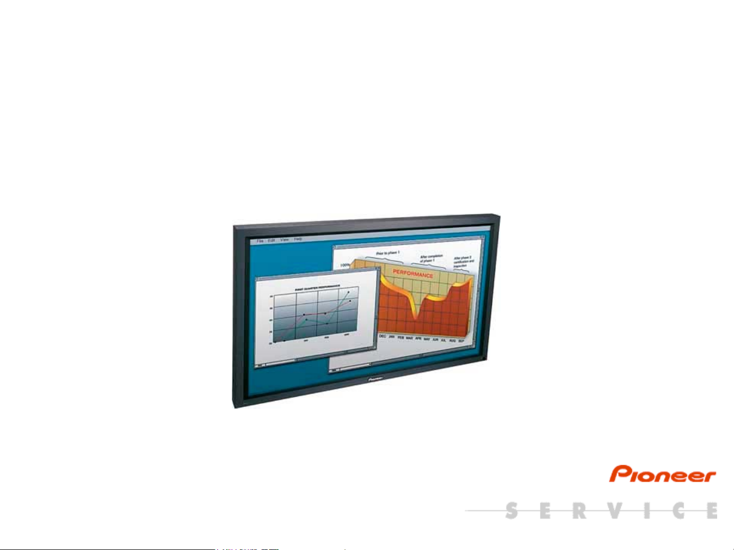
Product Training Guide
PDP-503CMX
Multimedia & Web Training Department
545 Nolan Drive Suite 100
Southlake, Texas 76092

Contents
Preface ……………………….…….. 3
New Functions…………………4-7
Basic Specifications.……………... 8
New Features ….………………..…. 9-18
Controls & Connectors…………………41-45
Normal Operation & Menu Modes……46-65
Main PCB layout………….…………19
Overall Block………………..…20-21
Overview…………………………..…22
Video Card………………………...…23-24
RGB Block……………………….…..25-28
Digital Video………………………...29-30
Y Drive…………………………….….31-32
X Drive…………………………….….33-34
Sub Address………………………...35-36
Resonance & Mid Clamp…….……37-38
Fan Drive/Audio…………………….39-40
Integrator Modes………………………...66-93
Disassembly……………………………...94-97
Factory Service Modes………………….98-132
Adjustments……………………………..133-145
PCB Locations………………………….146
Shut Down & Power Down……………147-155
RGB/Digital Video Replacement…….156-157
Preface
This technical training guide will address
the disassembly and adjustments of the
Pioneer PDP-503CMX Plasma Display.
This guide was designed as a servicing aid
and is not intended to replace the service
manual. The student should have the
appropriate service manual on hand when
when using this guide. Data in the service
manual for this unit contains specific
information on safety, parts and adjustments.
Safety information
Important safety data for this Pioneer model
is contained in the service manual. Before
returning the unit to the customer, complete
all product safety obligations and tests.
Technicians who bypass safety features or
fail to carry out safety checks may expose
themselves and others to possible injury,
and may be liable for any resulting damages.
For more information on electronic
circuits and block diagrams refer
to Service manual ARP3093
Lead in the solder used in this product
is a known reproductive toxicant which
may cause birth defects or other reproductive
harm. (California Health and Safety Code
Section 25249.5).
When servicing this or handling circuit
boards and other components which
contain solder, avoid unprotected skin
contact with the solder. Also, when
soldering do not inhale any smoke or
fumes produced.
3

List of New Functions
4
1. Out of Menu Mode
AUTO SET UP
• A function to adjust SCREEN mode automatically.
• The results of the adjustment is reflected on SCREEN value in Menu Mode.
• It functions only in case of PC signal input. (INPUT 1 or 2).
POINT ZOOM
• A function to magnify a display picture.
• The magnifying powers are 1.5 times, 2 times, 3 times, and 4 times
• When setting "POINT ZOOM", the picture size becomes "FULL mode".
• It functions only in the case of PC signal input.
Levels Display
• A function to display a setting content in OPTION menu.
• It displays by pressing the "DISPLAY CALL" key more than 2 sec. during an OSD display by usual DISPLAY CALL.
• Able to control this function using a new RS-232C command (DS2).
STILL
• A function to make a still picture from a present picture on the monitor.
• Able to set up using RS-232C command (SLY/SLN).

2. In Menu Mode
5
AUTO FUNCTION
• A function to switch to this input automatically, when a signal is
inputted to the input which was selected by this setting.
Automatically it goes back to previous input when there is no
input signal in the input.
• This function works only with “INPUT1” and “INPUT4”.
• For the “INPUT1”, this function works only with Composite
SYNC and Separate SYNC.
POWER CONTROL
• To switch the settings “Normal Display”, “Linear Brightness”, and
“Power Save”.
1. Normal Display : Almost the same as PDP-502 setting
“ABL ON”
2. Linear Brightness : Almost the same as PDP-502 setting
“ABL OFF”
3. Power Save : New function from PDP-503
A function to lower the peak brightness
and lowers power consumption.
• Able to set up using RS-232C command (1: PWN / 2:PWS /
3:PWL)
PURECINEMA
• A function to convert 480i to 480P based on 2-3 pull-down data.
• There are three settings; OFF, STANDARD, and HQ.
• Able to set up input signal NTSC/480i only
• Able to set up using RS-232C command (PUN/PUS/PUH)
DIGITAL NR
• Setting up digital noise reduction.
• There are four settings; OFF, LOW, MIDDLE, and HIGH.
• It is effective only in the case of a VIDEO (NTSC) signal input.
• Able to set up using RS-232C command (NRN/NRL/NRM/NRH)
COLOR TEMP
• A function that changes setting of the colors TEMP.
• There are six settings: LOW (approx. –3000K), MID LOW
(approx. –2000K), MIDDLE(+/- 0K), MID HIGH(approx.
+1000K), HIGH(approx. +2000K)
• It is effective only in the case of a VIDEO (NTSC) signal input.
• Able to set up using RS-232C command
(CT1/CT2/CT3/CT4/CT5)
INPUT LABEL
• A function to change “INPUT LABEL” of each input.
• It is able to set up max. of eight letters.

3. Integrator Menu
6
OFF TIMER
• A function to switch to Stand-by mode after a set time.
• This setting has OFF,
TIMER (1 to 24H/ every 1H)
MASK (0.0 to 9.5 H/ every 0.5 H)
MASK Color (WHITE /RED / GREEN/ BLUE)
2 by 2 mode
• A function to make temporally 4 screen multi-display.
• This setting has ON or OFF and display area (upper left/ lower
left/ upper right/ lower left).
• Able to set up using RS-232C command (MGY/ MGN/ MG1/
MG2/ MG3/ MG4)
INVERSE
• A function to control burned display by reversing output picture.
• The setting has ON or OFF.
• Able to set up using RS-232C command.
ID SET
• A function to set or change ID No.
MONITOR NAME
• A function to register a name with each unit.
• Able to set max. of twelve letters.
• Able to confirm the name by Display Call/ GET command
ORBITER
• A function to control burned display by shifting picture location
for every moment.
• The setting has ON or OFF
• Make the picture location shift one dot by one dot horizontally or
vertically every eight minutes.
• Able to set up using RS-232C command (OMY/OMN).
HDTV Mode Setting
• A function to set actual line number in HDTV (1080i/1035i)
• Able to set this function when signal mode is “12/13”
• Able to set up using RS-232C command
(1080i=H80/1035i=H35)

4. Service Factory Menu
7
5. RS-232C
Displaying / Setting Pulse Meter
• A function to display or set the present pulse meter.
• The display is ten million unit
• The setting is hundred billion unit.
• Able to set up using RS-232C command.
Pulse meter display: PMD
Pulse meter setting: PMS+ XXX
Writing setting in EEPROM for Plug & Play use
• Releasing Write-protection of EEPROM for Plug & Play use.
• Able to set only in service factory mode and RS-232C factory
adjustment mode.
When it exits the above modes, it returns to Protect setting.
• Able to set up using RS-232C command.
Write protect release: EWY
Write protect setting: EWN
Picture mute ON/OFF setting
• A function to set Picture MUTE on or off.
• No Last Memory function.
• MUTE is canceled when other operations are conducted.
• Able to set using RS-232C command only.
• It is effective in case of only Normal mode/ RS-232C adjustment
mode/ RS-232C factory adjustment mode.
Drive ON / OFF Setting.
• A function to set Drive circuit on or off.
• There is no last memory function. (After turning off a unit, this
setting is canceled)
• Able to set using RS-232C command only.
• The command is effective only in Standby mode and RS-232C
factory adjustment mode.
100 % display mode setting 100%
• A function to change screen display into 100 % display.
• It functions only in case of VIDEO signal.
• All of menu modes are prohibited during this setting.
• Able to set up using RS-232C command only.

Basic Specification
8
PDP-502MX/MXE
PDP-503CMX
PDP-433CMX
(Current model)
Screen size 50inch 50inch 43inch
Aspect ratio 16:9 16:9 16:9
Number of pixels 1280(H) 768(V) 1280(H) 768(V) 1024(H) 768(V)
Pixel pitch 0.858 mm (RGB) 0.808 mm 0.858 mm (RGB) 0.808 mm
Gradation
Brightness
Contrast ratio 560:1
Viewing angle
Fan
(256 gray scale)
560cd/m2
H: More than 160°
V: More than 160°
4
4
(768 gray scale)
800cd/m2
800:1
H: More than 160°
V: More than 160°
2
2
0.930 mm (RGB ) 0.698 mm
(768 gray scale)
800cd/m2
800:1
H: More than 160°
V: More than 160°
2
Front filter Acryl Glass
Power requirements
Power consumption
Effective screen size
Dimensions
Weight
MX: 100~120V 50/60Hz
MXE: 100~240V 50/60Hz
470W
1098mm 620.5mm 1098 mm 620.5 mm
1218mm 714mm 98mm
40.3kg
MX: 100~120V 50/60Hz
MXE: 100~240V 50/60Hz
380W
1218mm 714mm 98 mm
38.9kg
Glass
MX: 100~120V 50/60Hz
MXE: 100~240V 50/60Hz
TBD
952.3 mm 536.1 mm
1070mm 630mm 98mm
Less than 30kg
NEW Features/Benefits
9
• PDA-5002
– When installed it
adds Video, YC, and
DVI input, as well as
enabling High
Definition.
– Card manufactured
and supported by
Pioneer.
PDA-5002
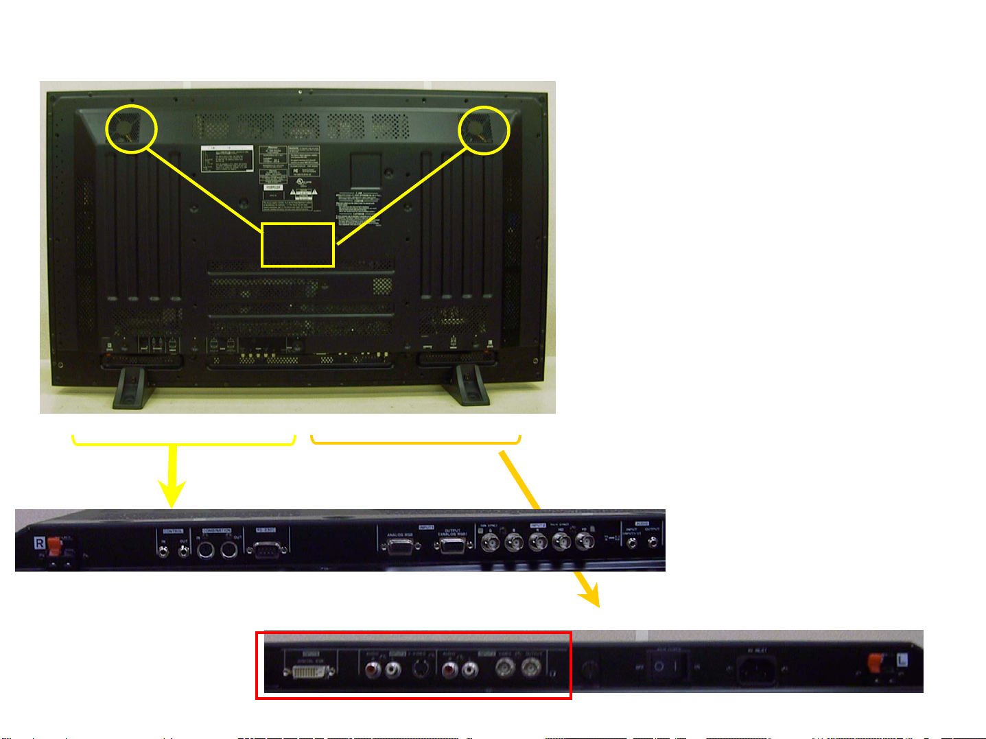
Rear View & Terminals
10
FAN
503CMX
RGB/BNC*5 In x1
RGB/D-Sub In x 1
RGB/D-Sub Out x1
Audio/Mini LR In x1
Audio/Mini LR Out x1
Speaker LR x1
Control
RS-232C/D-Sub 9 x1
SR/Mini In+Out x 1
Combi/Mini Din 6 In/O x1
PDA-5002
DVI-D In x1
YC/S VHS In x1
Composite/BNC In x1
Composite/BNC Out x1
Audio LR/RCA x2
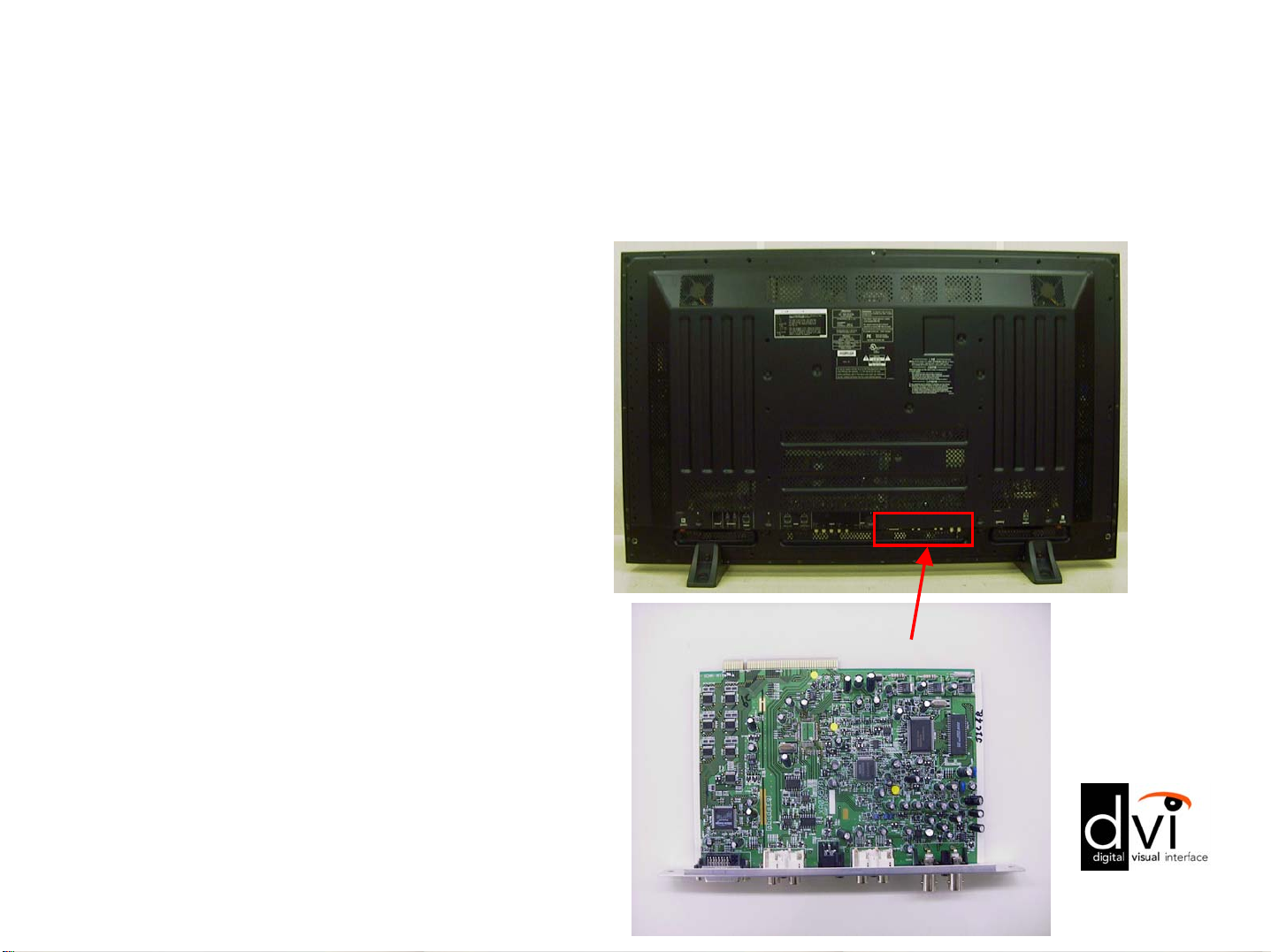
PDA-5002 (VIDEO CARD)
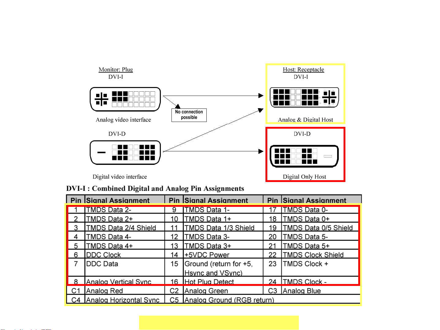
DVI-D interface for PDA-5002
11
There are two types of DVI interface; DVI-D and DVD-I. PDA-5002 has DVI-D input. Which
means this terminal can only accept Digital RGB signal.
Also the cable must be DVI-D cable.
(Yellow square)
DVI-I cable can not be used for PDA-5002.
Technical explanation on the new features.
12
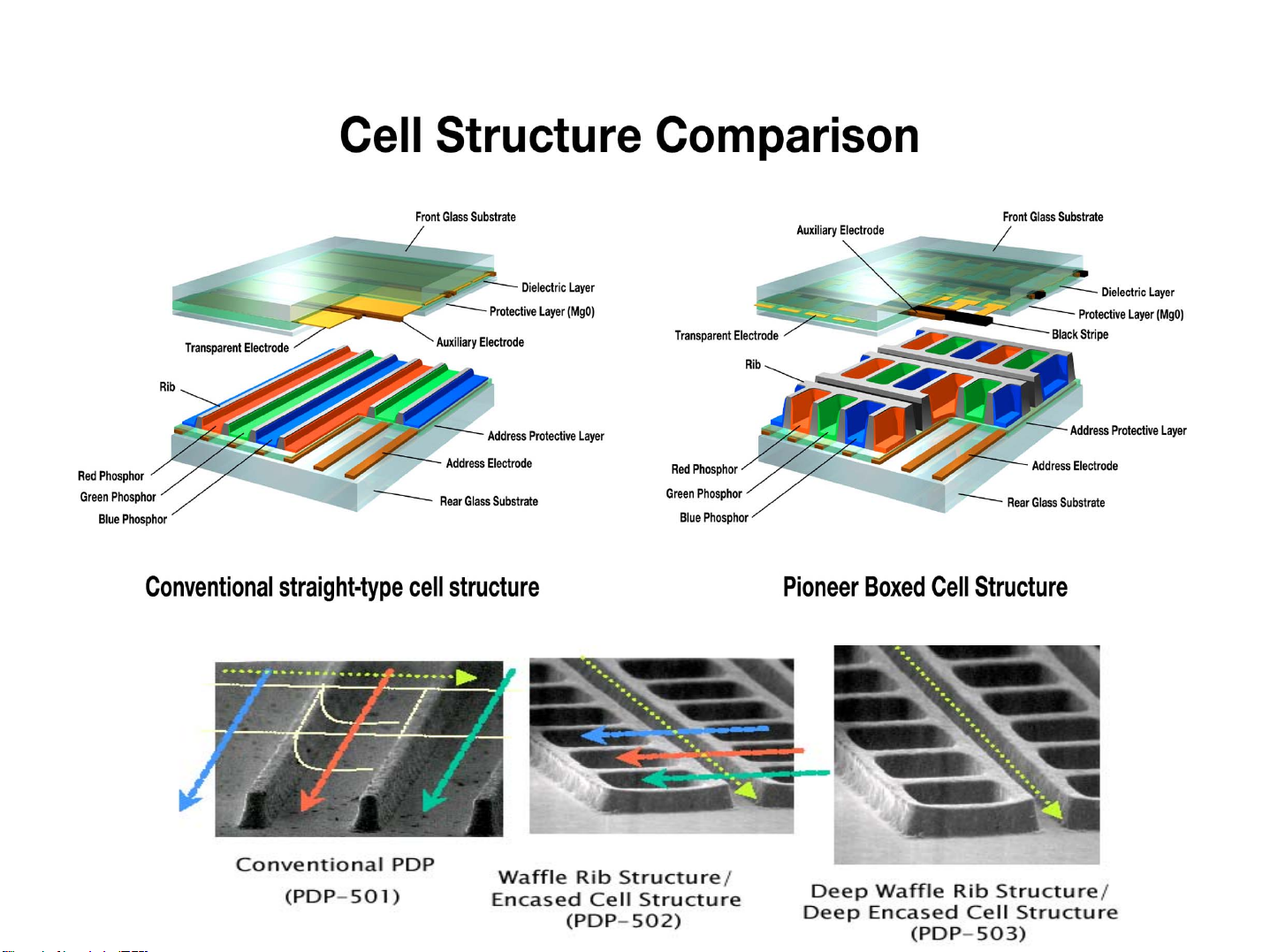
Higher luminance is realized by changing the cell structure.
- Higher luminance and contrast -
2. Technical explanation on the new features.
2. Technical explanation on the new features.
- Higher luminance and contrast -
- Higher luminance and contrast -
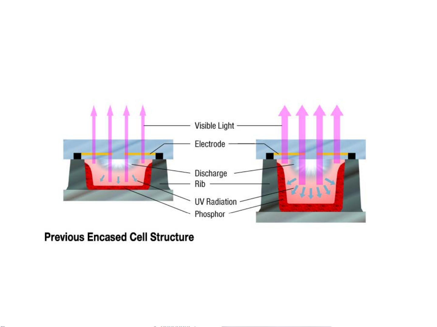
Deep Waffle Rib Structure: realises even higher light emission
13
efficiency
For the PDP-503, Pioneer’s further improved this technology
by making each individual cell deeper.
Deep Waffle Rib Structure
(Deep Encased Cell Structure)
The new cell structure has a greater light emission area, so this results in
even higher light emission efficiency—50% higher than our previous model .
(PDP-502)
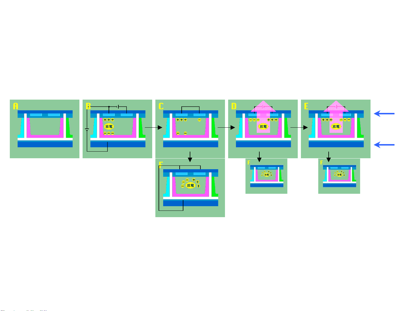
PDP basic principles
14
The PDP screen is 2 glass panels with pixels sandwiched. The pixels consist of tiny
cells with electrodes on the top and bottom. Inert gas (Xenon+Neon) is trapped
between 2 glasses, separated by a gap of just 100-200 microns wide. UV light is
generated by discharging the gas using electrodes. Red, green and blue phosphors
absorb these UV discharges and reradiate the energy as visible light to produce the
colors that appear on the screen.
Sustain
electrode
Address
electrode
Pioneer Method
[B-C] Initialization discharge
(Reset) charges the electric at
+/- electrodes, activating
gas to extract electron
[F] Address discharge selects the cells
required for emission by clearing the
electric charge from unnecessary cells
with comparatively small voltage
[D] Sustaining discharge is made by a pulse of voltage on sustain electrodes. It
generates UV light, which makes phosphor radiate visible light emission.
[E] The electric at electrodes remains so that continuous pulses of AC voltage
can make another light-emitting discharge
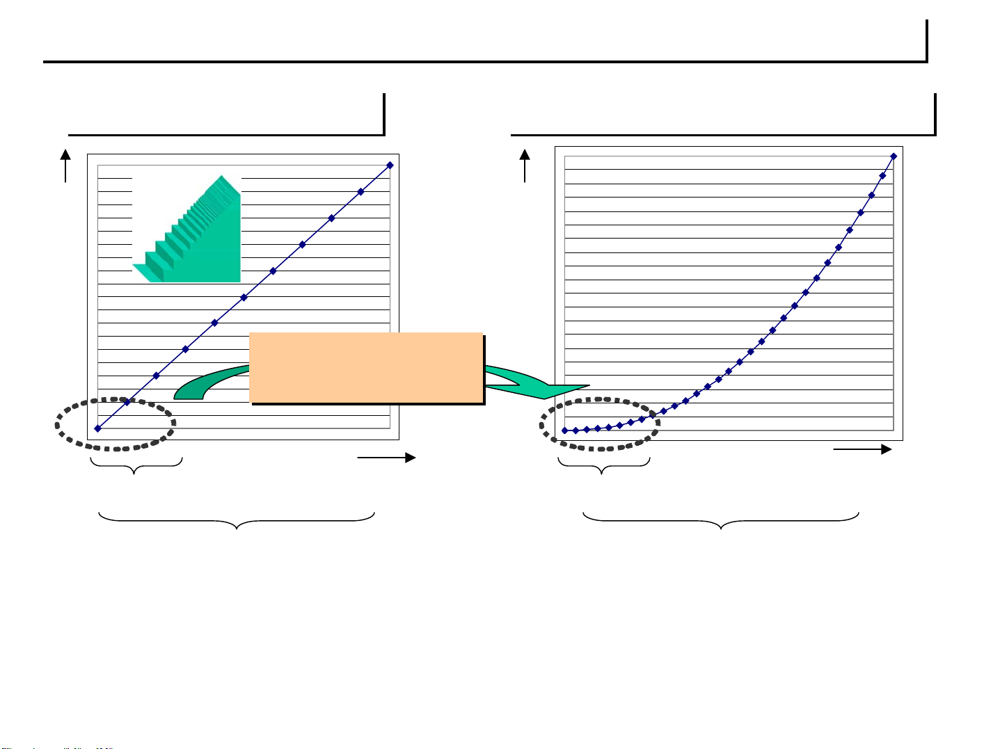
Improvement of gradation reproduction in low brightness range
15
Improvement of gradation reproduction in low brightness range
General PDP
General PDP
Output/ Brightness
16 times
16 times
(lowest 5% range)
(lowest 5% range)
Input
New CLEAR drive system
New CLEAR drive system
Output/ Brightness
12 steps 200 steps
Input
256 steps (8bit Sub field method)
•Linear shaped characteristics of brightness level against input signal of conventional PDP is
poor at gradation in low brightness range
•Allocating comparatively more steps in low range, Characteristics of 503 has a gamma curve
similar to analog CRT, which doesn’t require the artificial process for offsetting gamma curve
of input signal in video processing
768 steps (grayscale/ NTSC)
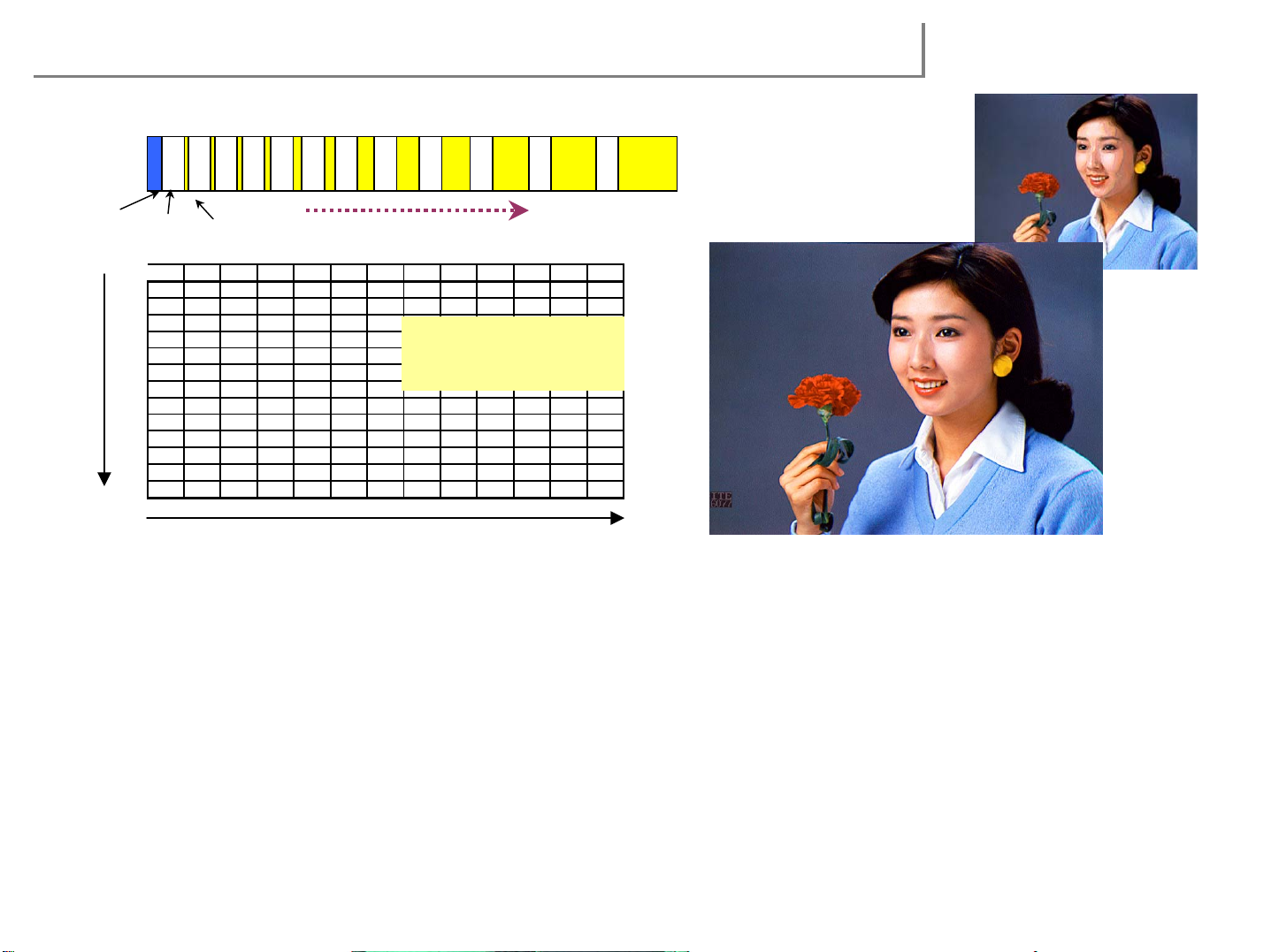
CLEAR driving method: the way to increase gradations
16
CLEAR driving method: the way to increase gradations
502MX:
12 sub-field x 2 (Field-to-field offset alternating) x 16 (Dither & Error dispersion) = 384 gradations
503CMX:
Sub-field Field-to-field offset alternating Dither & Error dispersion Total gradations
PAL 13 x 2 x 32 = 832
PC 10 x 2 x 32 = 640
NTSC 12 x 2 x 32 = 768
1
1st Field
2nd Field
0.5
0
0612
Output luminance level
Field-to-field offset
1
alternating
0.5
0
01224
Input Signal level
Each field (1/60 sec) can have 12 steps. (in case of NTSC)
With using 2 neighboring fields, different grayscales are
assigned. By combining these 2 fields, grayscales inbetween can be generated. As a result of it, another 12
steps can be implemented to get 2 times as many
grayscales as that of 1 field.
1
Dither & Error
dispersion
0.5
0
01224
Dithering & Error dispersion
method realized by 10bit precise
calculation refines the analog-like
smooth gamma curve
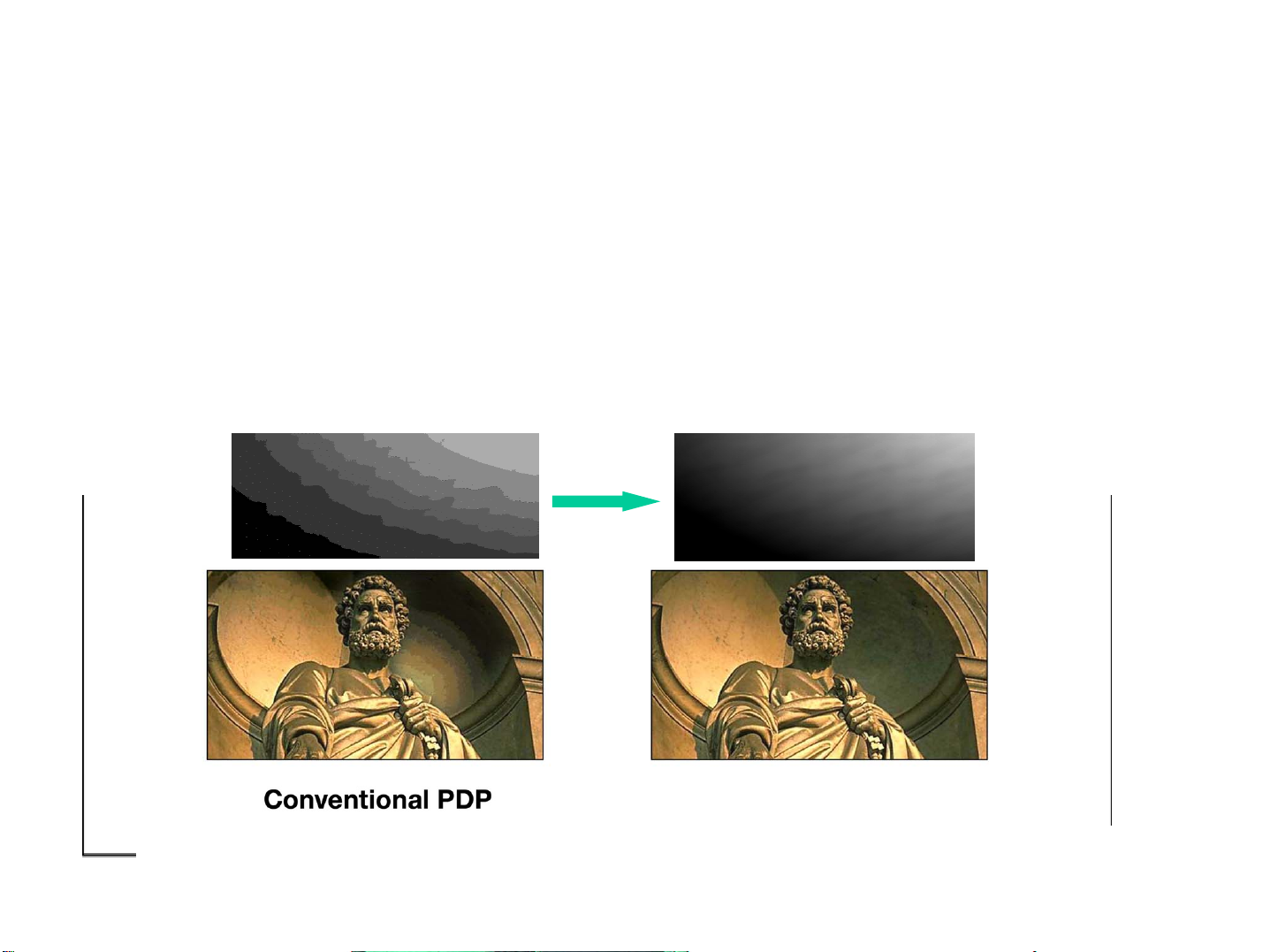
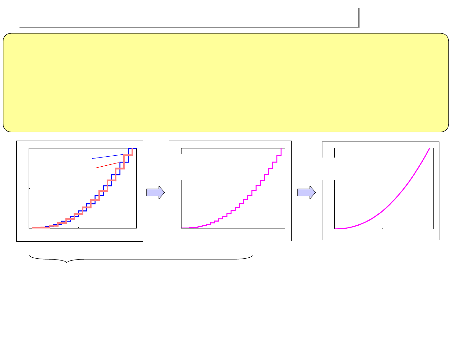
Gradation Reproduction in Low Brightness Range
17
Pioneer’s CLEAR* driving technology has succeeded in eliminating
false contour of poor gradation areas. Details in shadow that were
previously obscured in conventional PDP can now be seen.
(*CLEAR: high-Contrast & Low Energy Address & Reduction of false contour
sequence. We alternatively call it “Continuous Emission Display Technology”)
Even with dark images, detailed patterns are faithfully reproduced.
Pioneer CLEAR drive
Conventional PDPs exhibit rough gradations in the low brightness
range, so image quality in dark areas is inferior. Pioneer’s gradation
slope is much smoother.
CLEAR sub-field driving method
›
›
›
›
›
›
›
›
›
›
›
›
›
›
›
›
›
18
CLEAR sub-field driving method
Continuous Emission Display Technology
Reset
Address Sustain
IT NOLSB 2BIT 3BIT 4BIT 5BIT 6BIT 7BIT 8BIT 9BIT 10BIT11BITMSB
0
1
2
3
4
5
6
10
11
12
7
8
9
Grayscale
›
› ›
› ›
› › ›
› › ›››
› › ››› ›
› › ››› ›
› › ››› › ›
› › ››› › ›››
› › ››› › ››› ›
› › ››› › ››› ›
Continuous
light emission
bright
Time (1/60 sec, NTSC)
•Only one reset discharge per field
•Continuous light Emission of the needed number of pulse
•No random light emission = No more random gaps without emission
Results :
•Higher Contrast (Lowest brightness less than 1cd/m2)
•Less Addressing power consumption: 1/3 vs 501
•No Dynamic False contour
High Contrast & Low Energy Address & Reduction of false contour sequence
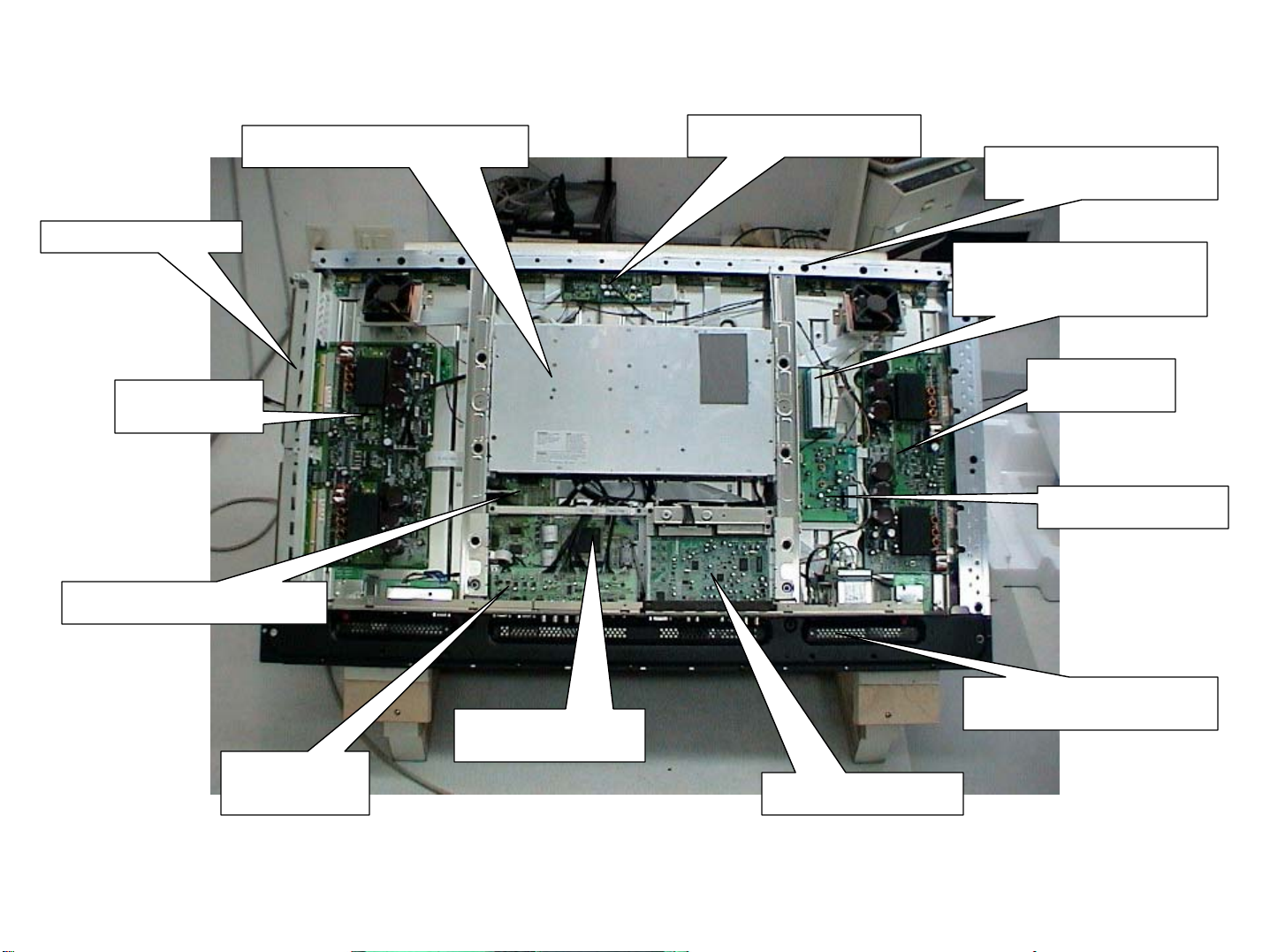
Main PCB Layout PDP503CMX
19
Scan Modules
Y-Drive
Digital Video Assy
Power Supply
Resonance Assy
Address Modules
V-Mid Clamp PCB
X-Drive
Audio Assy
Input Assy
Address Modules
RGB Assy
Video Card
B
T
U
L
G
E
V
V
P
S
R
20
IC
IC
IC
IC
IC
IC
IC
IC
IC
IC
IC
IC
IC
IC
IC
IC
IC
IC
IC
IC
IC
DRIVER
DRIVER
DRIVER
DRIVER
DRIVER
DRIVER
DRIVER
DRIVER
DRIVER
DRIVER
DRIVER
DRIVER
DRIVER
DRIVER
DRIVER
DRIVER
DRIVER
DRIVER
DRIVER
DRIVER
DRIVER
CLC1
CLAMP
CLAMP C ASSY
VADR2
ADDRESS CONNECT D
ASSY
AD1
CLK/LE
BUFFER IC
IC6901
BRIDGE C
ASSY
VADR2
BGC1
CLAMP
VADR2
ADDRESS CONNECT C
ASSY
AC1
CLK/LE
BUFFER IC
IC6881
VADR2
K2
ADR RESONANCE AS
Q6706 to Q6711
VADR_GEN
CLAMP A
ASSY
CLA1
IR
ASSY
SP OUT R
SPR1
C3
CONTROL ASSY
DRIVER
232C
C1
Plug&Play
E2PROM
REG
STB5V
IN1 DET
SEL
SEL
SW1
KL1
KL2
T4
12V,9V,±5V,3V
13.5V,6.5V,-9V
T1
T5
12V,
12V,13.5V,
-9V,6.5V
T2
STB5V
3ST
KEY CONNECTOR
ASSY
D17
9V,±5V,
3V
12V,13.5V,-9V,
6.5V,STB5V
T6
T3
+3
R
SIDE KEY
ASSY
D12
D13
RE
SCAN B ASSY
(LOWER)
LED_SIG
RE
I2
+3V,+5
SEL_PULSE
ADD
PSUS
MODULE
UCOM
IC120
TXD/RX
PANEL UCOM
IC1101
TXD0/RXD0
RB2:9
R6
SEL_PULSE
IC6006
IC5
VCC_VH
FLASH
ROM
V+3V_
RA2:9
+3V,+5V,-5V,+9V
ADD
IC119
16M
IC6005
SD RAM
VCC_VH
BLOCK
V+5V_STB
GB2:9
SEL_PULSE
IC6004
ADD
IC5
Photo Coupler
V_IC5V
ADLCLK_DR
V+3V_
GA2:9
BB2:9
SD RAM
16M
IC5102(IC101)
IC5001(IC102)
A/D P
VCC_VH
Y6
IC4
IC5
BLOCK
BA2:9
SEL_PULSE
Scan Signal
OFFSET
16M
16M
SEL_PULSE
IC6002
IC6003
ADD
ADD
VCC_VH
PSUS
IC5
IC5
VCC_VH
Y DRIVE ASSY
VC_VF-
V_OFSVC_VF+
For RIGHT with FILD MEM.
SUB-FILD CONV.
IC1401 (IC31
GB2:9
RA2:9
RB2:9
R3
SD RAM
SD RAM
3State Buffer
WIDE UCOM
SEL_PULSE
ADD
SCAN
V_IC5V
VCC_VH
SOFT-D
BLOCK
Y2
V+3V_I
C
V+2V_I
GA2:9
BB2:9
IC5301(IC30)
IC5601
IC6001
VCC_VH
BA2:9
IC5
Y5
+15V
R2
RGB ASSY
+3V,+2V
R4 R9
STB+5V
SEL_PULSE
IC6206
ADD
SCAN
Y3
BLOCK
Y-SUS
MASK
+5V VSUS+15V
Pulse Module
IC2204
Signal
Drive
BLOCK
LOGIC
YDRV_SIG
SCAN_SIG
CLK GEN
for LEFT with FILD MEM.
SUB-FILD CONV.
IC1301(IC31 L)
V+5V_ST
SEL_PULSE
IC5
VCC_VH
V_IC5V
VCP
+RESET Block
X180
V+3V_
V+2V_IC
V+3V
ADD
V+3V
IC6205
VCC_VH
VCC_VH
V+2V
SEL_PULSE
ADD
IC5
Pulse Module
+15V
IC2206
VSUS
Signal
Drive
+5V
TEMP
XY DRV SEQUENCE
PATTERN GEN.
ADL_LE_UL
ADL_LE_DL
XDRV_SIG
P1
P2
P5
P6
IC6204
VCC_VH
PSU
BLOCK
MASK
IC1703
IC5
Y-SUS
+5V VSUS+15V
Y1
KL_U0:2
SEL_PULSE
SEL_PULSE
IC6203
ADD
ADD
IC5
VCC_VH
Y4
VCP
VC_VF+
VC_VF-
BLOCK
DC/DC
CONV
12V
V+3V
DIGITAL ASSY
V+2V
VADR
VSUS
VS
SEL_PULSE
IC6202
ADD
IC5
VCC_VH
PSUS
V_OFS
VCC_VH
V_IC5V
V+5V_STB
+12
DC-DC CONVERTER
MODULE
V+3V
+12V
+15V
T102
Switching
Q117
T103 T104
Switching
Q119
Switching
IC6201
VCC_VH
+12V
V+5V_
IC5
TE1
D8
D9 D16
-9V
Q115
(UPPER)
+6.5V
T101
Switching
SCAN A ASSY
THERMAL SENSOR
ASSY
+13.5V
POWER SU
SAA1 SAA2
+60
SAA3
ADR_CO
RE1
ASSY
L OUT
SR IN SR OUT
Combi
IN
Combi
OUT
RS-232C
Component/
RGB
INPUT 1
OUTPUT
INPUT 2 INPUT 1/2/5
Component/
RGB
Audio
IN
SAB2
ADR_C
SAB3
K1
+60
SA
OUT
Audio
CLAMP
ASSY
AA1
BGA1
CLAMP
BRIDGE A
ASSY
AB1
ADR RESONANCE
ASSY
K2
Q6706 to Q6711
VADR_GEN
K1
VADR2
ADDRESS CONNECT A
CLK/LE
BUFFER IC
IC6501
VADR2
VADR2
ADDRESS CONNECT B
ASSY
CLK/LE
BUFFER IC
IC6601
VADR2
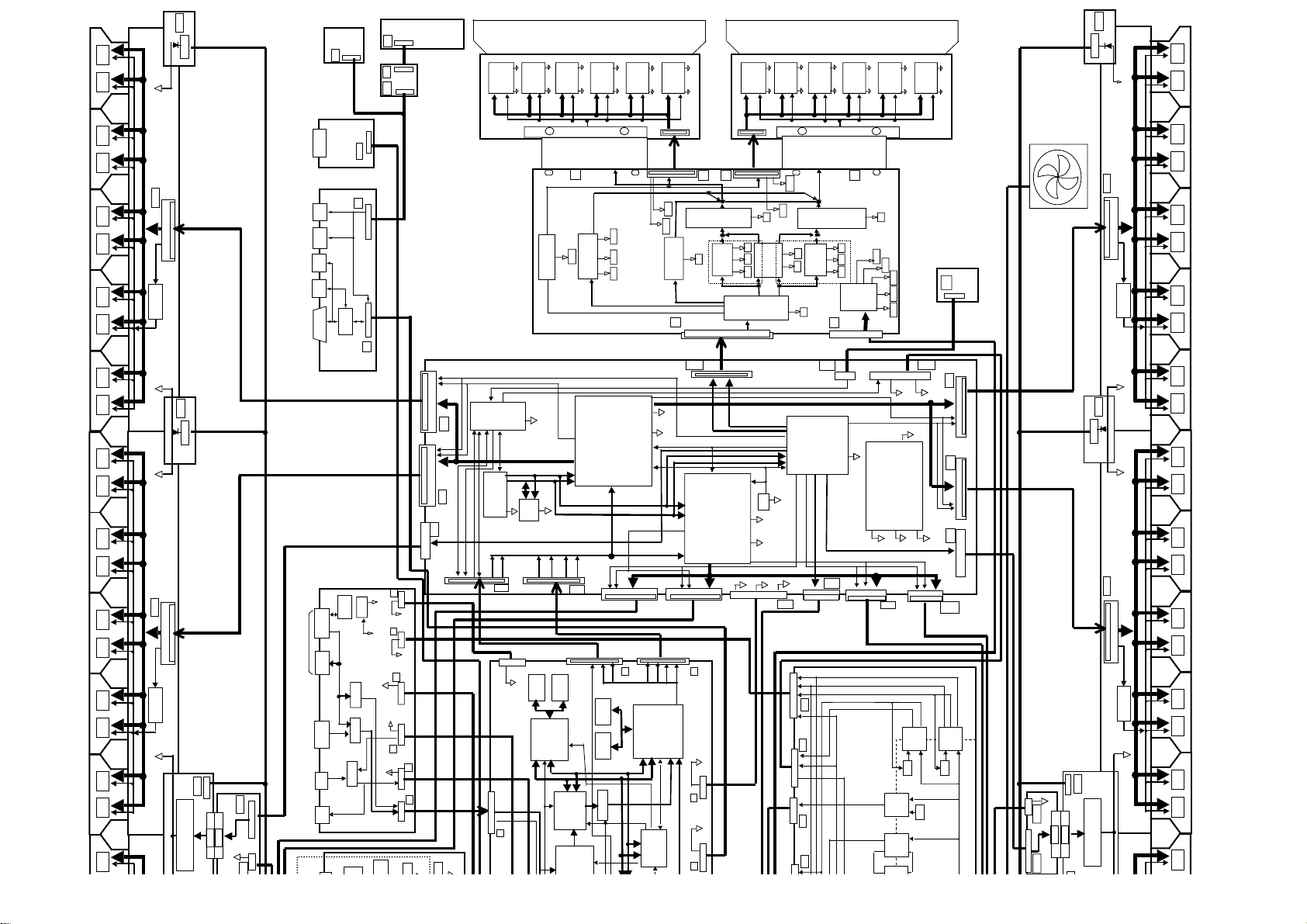
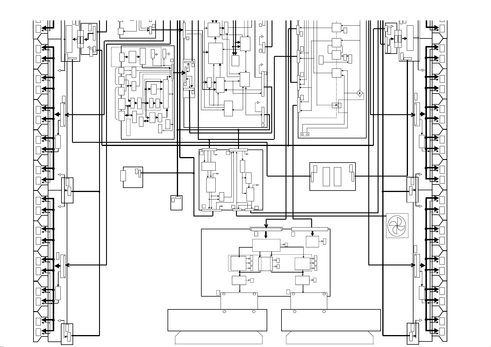
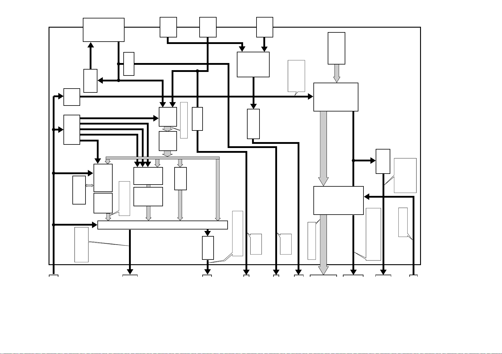
Overall BLOCK DIAGRAM
DRIVER
IC
DRIVER
IC
DRIVER
IC
DRIVER
IC
DRIVER
IC
DRIVER
IC
DRIVER
IC
DRIVER
IC
DRIVER
IC
DRIVER
IC
DRIVER
IC
DRIVER
IC
DRIVER
IC
DRIVER
IC
DRIVER
IC
DRIVER
IC
DRIVER
IC
DRIVER
IC
DRIVER
IC
DRIVER
IC
DRIVER
IC
E
o
2
K
R DRIVER
21
IC
BLOCK DIAGRAM
OVERALL BLOCK DIAGRAM
DRIVER
IC
DRIVER
IC
DRIVER
IC
DRIVER
IC
DRIVER
IC
DRIVER
IC
DRIVER
IC
DRIVER
IC
DRIVER
IC
DRIVER
IC
DRIVER
IC
DRIVER
IC
IC
IC
IC
IC
IC
IC
IC
IC
IC
IC
IC
IC
IC
R DRIVER
DRIVER
DRIVER
DRIVER
DRIVER
DRIVER
DRIVER
DRIVER
DRIVER
DRIVER
DRIVER
DRIVER
DRIVER
2
ADR RESONANCE ASSY
Q6706 to Q6711
VADR_GEN
SAB3
K1
K3
VADR2
AB1
CLK/LE
ADDRESS CONNECT B ASSY
BUFFER IC
IC6601
VADR2 VADR2
BGD1
CLAMP
BRIDGE D ASSY
ADDRESS CONNECT A ASSY
SAB2
ADR_C
+60
SAB1
SUB ADDRESS B
ASSY
OUT
INPUT 5
DVI-D
Audio
INPUT3
S-Video
Audio
Composite
INPUT4
OUTPUT
VIDEO SLOT
ST1 ASSY
Audio
L OUT
Receiver
IC7401
TMDS
SEL
IN3 DET
6M LPF
SEL
IN4 DET
AWV1906 Only
SPL1
SP OUT L
ASSY
3STATE Buffer
SD RAM
REG
FLT
3L Y/C
&CNR
T3
+7V
SECAM
3D Y/C
+3V,+5V
6MLPF
6M LPF
Expander
R6
+3V,+5V,-5V
REG
+7V,-8V
V1
CHROMA DECODE (4-1SEL)
IC7302
I2C-BUS
E2PROM
L1
S3
SLOT CONNECTOR
ASSY
MX LED ASSY
3State Buffer
IC5001(IC102)
A/D PLL AMP
IC4603
FLASH
MATRIX
PLD for SYNC
+15V,+5VSTB
A5
+15V
D.C Det
+5VSTB
IC4803
ROM
I2C-BUS
Audio_NG
Temp3
A7
FAN_NG
OP-AMP(Buf)
S1 S2
6M LPF
L_Audio
R_Audio
A1
A_Mute2
Audio
Mute
POWER AMP
IC8601
R_OUT
L_OUT
A3
WIDE UCOM
IC5601
MAIN UCOM
IC5505
+5V_AD/RGB
FAN_Mute
REGULATOR
IC8701
R4 R9
STB+5V
STB+5V
R1
STB+5V
12V,5V
R8
MX AUDIO ASSY
+15V
FAN_D
A6
P5
P6
P3 P4
VADR
VSUS
M114
STB5V
POWER(RELAY)
VM1
T103 T104
VSUS_CONT
T105
T105
SECONDARY
V MID CLAMP U
V MID CLAMP L
Switching
PRIMARY
RL101
ASSY
Switching
Q119
Q122
M111
NEAUTRAL
LIVE
VM2
V MID CLAMP
+60
SAA1 SAA2
POWER SUPPLY MODULE
ADR_CO
ASSY
RC101
Q6706 to Q6711
VADR_GEN
SAA3
K1
SUB ADDRESS A
K3
ASSY
BGB1
CLAM
BRIDGE B
ASSY
VADR2
AC1
CLK/LE
ADDRESS CONNECT C
BUFFER IC
IC6801
VADR2 VADR2
IC
IC
IC
IC
IC
IC
IC
IC
DRIVER
DRIVER
DRIVER
DRIVER
DRIVER
DRIVER
DRIVER
DRIVER
AA1
CLK/LE
BUFFER IC
IC6501
VADR2
CLD1
CLAM
CLAMP D ASSY
X CONNECTOR
B ASSY
X DRIVE ASSY
X4
Module
Pulse
MASK
Signal
IC3201
X_SUS
Drive
P_SUS
+15V+5VV_SUS
VCP
DRIVER
CLK/LE
IC
IC
IC
IC
IC
IC
DRIVER
DRIVER
DRIVER
DRIVER
DRIVER
DC/DC
CONV
VCP
V_SUS
+15V+5V
V_RN
AD1
ADDRESS CONNECT D
ASSY
BUFFER IC
IC6901
V_RN
+15V
X 1
BLOCK
Signal
Drive
+5V
Module
IC3200
Pulse
X_SUS
MASK
P_SUS
X3
X2
BLOCK
LOGIC
+Reset
Pulse
Block
X CONNECTOR
A ASSY
CLAMP B
ASSY
CLB1
CLAMP
VADR2
IC
IC
DRIVER
DRIVER
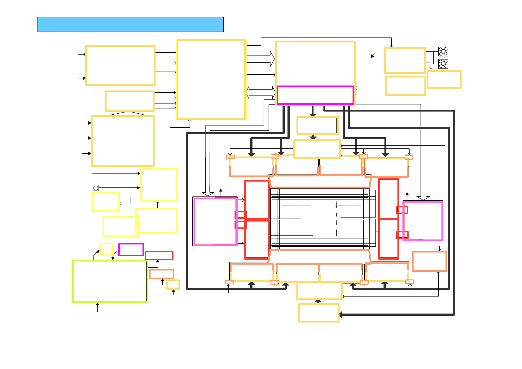
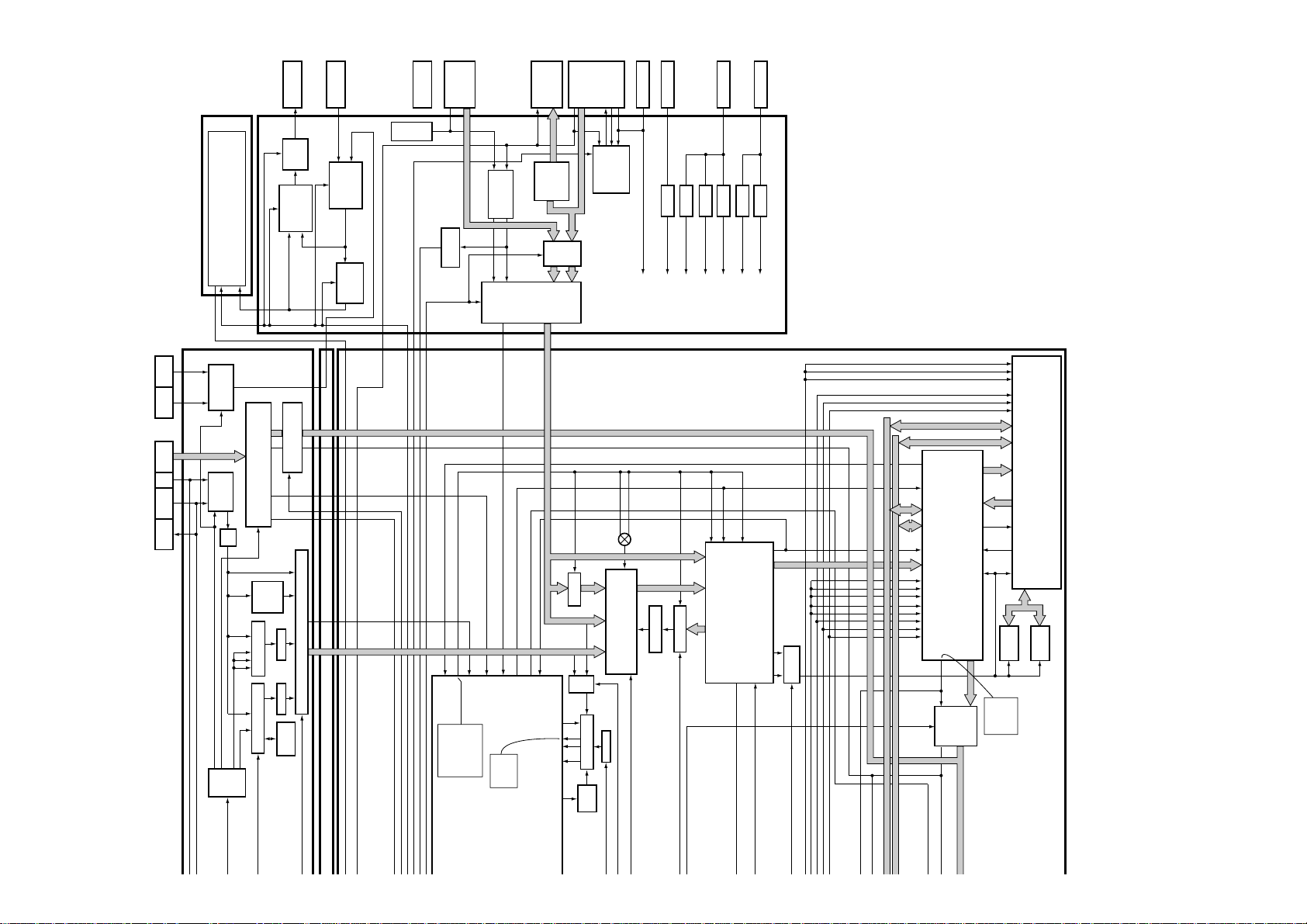
Overview PDP-503CMX.
22
–
IN1 RGBin
(Dsub15)
IN2 RGBin
(BNC)
*Component in
with PDA-5002
IN3 S in
(Din6p)
IN4 C.Vin
(BNC)
IN5 DVI-Din
RS232C in
Cont in/out
Combi in/out
REM IN
Power Supply Assy
* SW P.S for STBY / Low / ADR
/ VSUS Voltage.
* PD Control
* Power factor improver
RGB I/O Assy
(AWZ6631)
* IN1/2 Terminals
* IN1/IN2 input RGB/SY select
* Mini/Pin Audio select
* Low Voltage regulators
(3/5/9/12V)
SLOT Connect Assy
(AWZ6634)
* Slot card interface
Video slot Assy, PDA-5002
(AWV1906)
* IN3/4 Terminals
* IN3/IN4 input select
* YC seap
* Color decoder
* DVI-D terminal, TMDS
decoder
IR Receive assy
Control assy
AWZ6643
* Vol level conv
IND assy
(AWZ6642)
* LED
Side SW assy
(AWZ6637)
Key cont assy
(AWZ6638)
* Key matrix
* Key SW
STB
+5V
PWR on/off
PD cont
(AXY1053)
AC IN
RGBHV
YPbPr
Audio
YCbCr
RGB
HV
Audio
(AW6633)
decoder
Vsus +230V
Vadr +60V
RGB Assy
(AWZ6632)
* RGB decoder for video signal
* A/D converter
* Digital video processing
( Picture control )
* IP conversion
* OSD addition
* Image size control (WIDE)
* Sync control
* System control CPU
(Key/Remote/Temp/FAN/
Comm with module CPU)
* TH sensor (Temp2)
Y DRV Data & Sel data
Adr Data
CL A assy
Key
Tx/Rx
Rem
(AWZ6650)
Vsus
+230V
Y Drive assy
(AWZ6645)
* Sustain Y Drive
* Select pulse buffer
* D-D Conv for
VH/Vofs/Vf
CL C assy
Vcc
(AWZ6652)
Digital video Assy
* Dither/Error dispersion
RGB dat 2ch
* Sub-Filed conversion (L/R)
* Field Memory
* Drive sequence gen.
* DC-DC Conv for Low voltages
HD/VD/CLK
S-Data
used within this assy.
* Panel control CPU (Panel drive)
* Module control CPU
(Comm with system/panel CPU/
Power control, PD control )
Adr Data
Br A assy
(AWZ6620)
ADR connect A
(NSP)
* Dat line buffer&latch
* Dat line buffer&latch
* Select pulse add
* Y Drive
Sel
data
Psus
Scan A
(NSP)
* Select pulse add
Psus
* Y Drive
Scan B
(NSP)
Sel
data
ADR connect D
(NSP)
* Dat line buffer&latch
Vadr
Br C assy
(AWZ6622)
* Dat line buffer&latch
Audio/FAN/
(AWV1903)
Temp3
MX Audio Assy
PWR On/Off
PD cont
(AWZ6644)
* Audio AMP
* FAN Drive
TH Sensor assy
Temp1
(AWZ6639)
* Thermal sense
X DRV Data
Reso data
Sub ADR A Assy
(AWZ6646)
*Adr Fault det
ADR Reso Assy
VadrVadr
ADR connect B
(AWZ6630)
*ADR Voltage gene.
(NSP)
Address ICs
* Latch & Upper Address drive
PDP PANEL
Reso data
ADR connect C
* Dat line buffer&latch
X 40
(NSP)
3840 ADR
384 X,Y
(NSP)
Vadr
Adr Data
Br B assy
(AWZ6621)
ADR connect D
(NSP)
* Dat line buffer&latch
Psus
X connector A
Bottom voltage
CL B assy
(AWZ6651)
+230V
(NSP)
* connetor
Psus
(1280 x 768)
384 X, Y
3840 ADR
Psus
(NSP)
* connector
Address ICs
X 40
(NSP)
X connector B
* Latch & Lower Address drive
ADR connect C
(NSP)
ADR Reso Assy
Vadr
(AWZ6630)
*ADR Voltage gene.
Sub ADR BAssy
(AWZ6647)
ADR connect B
* Dat line buffer&latch
(NSP)
Vadr
Reso data
ADR connect A
(NSP)
* Dat line buffer&latch
Br D assy
(AWZ6623)
*Adr Fault det
FAN (AXM1040)
SP out assy L/R
* Terminal
* Thermal sense (L)
Adr Data
Vadr
Vsus
X Drive assy
(AWV1901)
* Sustain X Drive
* D-D conv Vrn
V MID CLP
(AWV1934)
* Bottom Vol clamp
CL D assy
(AWZ6653)
Vadr
Bottom voltage
(Composite)
23
AKX1051
CN7001
Input 4
IN OUT
(Audio In)
DKB1031
JA7003
Input 4
AKP1217
(Y/C In)
Input 3
CN7002
(Audio In)
DKB1031
JA7004
Input 3
VIDEO CARD (PDA-5002)
DVI-D Terminal In
AKP1216
CN7402
Input 5
24LC01B
IC7104
CXA1875AM
Expander
IC7103
IS41C16256-35K
SD RAM
Y : K7303 → No.4
CB : K7302 → No.5
Video Driver
TK15420M
IC7001
UPD64082GF-3BA
3D Y/C & CNP
IC7202
IC7203
ML6428CS-1
6M LPF
IC7201
INPUT4 NTSC Color Bar
CR : K7301 → No.6
DET. Circuit
IN4 Signal
DVI PS
VY SEL
NT/PAL
M/N
BPF SW
INPUT4 NTSC Color Bar
3DY : K7201 → No.2
3DC : K7202 → No.3
CXD2064Q
IC7102
3D Y/C
ML6428CS-1
6M LPF
IC7105
2 - Selector
NJM2234M
IC7002
ML6428CS-1
6M LPF
IC7101
INPUT4 NTSC Color Bar
VY : IC7002 pin 7 → No.1
DET. Circuit
IN3 Signal
SECAM FLT
Chroma Decode (4 - 1 Select)
IC7302 TB1274AF
TC7WH04FU
IC7303
2 - 1 Selector
TC4052BF
UPC4570G2
IC7004
INPUT4 NTSC Color Bar
HD_PLD : IC7303 pin 7 → No.7
VD_PLD : IC7303 pin 5 → No.8
Hi : No Signal
Lo : Exist
IC7003
IN3_DET :
OTHERS : Lo
Hi : Normal Operation
Lo : Power Down
IN4_DET :
Hi : No Signal
Lo : Exist
DVI_PS
Input5 SELECT : Hi
RB_PLKO4 :
IC7407 pin 15 → No.10, 11
TMDS Receiver
TFP201A
IC7401
IC7402 - IC7407
3 State Buffer
LCX541FT
PLK_CNT [0 : 4]
DE_PLK : IC7307 pin 7 → No.9 - 11
VD_PLK : IC7307 pin 5 → No.9 - 12
TC7WH04FU
Inverter
CLK_PLK : IC7307 pin 7 → No.10, 11
HD_PLK : IC7307 pin 7 → No.9 - 12
IC7410
IC7410 pin 7 → No.12
VD_PLKU :
IC7410 pin 5 → No.12
SCDT :
Hi : Active Link
Lo : Inactive Link
Input5 SELECT : Lo
OTHERS : Hi
HD_PLKU :
SDA (pin 106)
SCL (pin 104)
CB (pin 5)
Y (pin 3)
CR (pin 7)
VD_PLD (pin 11)
HD_PLD (pin 9)
IN3_DET pin 118)
IN4_DET pin 117)
R (pin 15)
L (pin 13)
RA_PLKO [0 : 7](pin 154-161)
GA_PLKO [0 : 7](pin 142-149)
BA_PLKO [0 : 7](pin 132-139)
BB_PLKO [0 : 7](pin 54-61)
GB_PLKO [0 : 7](pin 42-49)
RB_PLKO [0 : 7](pin 32-39)
DE_PLK (pin 128)
HD_PLK (29)
VD_PLK (27)
CLK_PLK (pin 130)
VD_PLKU (pin 23)
HD_PLKU (pin 25)
SCDT (pin 126)
SDIN_SEL1 (pin 18)

Video Card (PDA-5002)
24
Input 3 : YC using a "S" connector and audio RCA X 2.
Input 4 : Composite in and out using (BNC) connectors
and audio RCA X 2.
Input 5 : DVI-D (Digital Visual Interface-Digital Host Only)
Audio can be connected to the main stereo mini
Jack for inputs 1 and 2.
Slot detect signal when inserted Is sent to the main CPU
Located on the RGB board. This allows inputs 3, 4 and 5
To be used as well as enabling High Definition signals
From inputs 1 or 2.
Signals from the DVI connector are sent through a TMDS
Receiver (Time Minimized Differential Signaling) and on
To the RGB board as 8 bit 2 phase digital RGB.

RGB Block
25
Main IC’s Function/Control
IC5505 Main System Microprocessor Module CPU, Wide Control CPU, Input
frequency sync detect, RS232 control,
Remote & key control, input switching, Fan
control and Thermal sensor monitor
IC4803 Sync Processing Generates sync for OSD with no input,
separates and processes all sync inputs
except DVI and sets clamp levels for sync
output to I/P selector IC
IC5301 Digital Video Processor Adjusts screen size, digital video enhance,
On screen display generator, 8 to 10 bit
converter (dither & error dispersion control)
IC4603 AD Converter Converts all input analog video signals to
digital RGB (8 bit) except DVI
IC4402 RGB Decoder Converts Y/PB/PR and Y/CB/CR signals to
RGB and outputs to the A to D converter
IC5102 & 5001 I/P Converter & Selector Converts input digital RGB signals from
Interlace to progressive and from 8 bit one
phase input to 8 bit 2 phase output
13.5V
V+12V V+12V
IC4004
6.5V
-9V
IC4110
(24LCS21A)
Plug&Play
ROM
(LT1399CS)
3CH
Video
Amp.
(TC74VHC541)
TTL
Conv.
INPUT1
Input DET.
IN1DET
WP_SW
Time
Circuit
IC4108
(BA7657F)
RGB
2-1 SW
STB+5V
INPUT1
Component
/RGB
INPUT2
Component
/RGB
Terminator
SW
Audio
Input
Mute
A_MUTE1
EXT_INT
VOL
IC4103
(TC4052BF)
EXT/INT
SEL
IC4104
(TA7630P)
Pre-Amp.
2-1
SEL
2-1
SEL
(LCX541)
Line Buffer
6M
LPF
SECAM
FLT
6M LPF
3L Y/C
3D Y/C&CNR
Audio
Input A
IC4103
(TC4052BF)
FIX/VAL
SEL
Audio
Output
Terminator
SW
INPUT1
Monitor
Out
V-5V V-5V
IC4001
FIX_VAR
A_MUTE2
AUDIO_NG
STB+5V
V+9V V+9V
IC4002
V+5V V+5V
IC4003
V+3.3V V+3.3V AD
IC4005
V+3.3V V+3.3V PLD
IC4006
Audio Amp.
Audio
Input B
DVI
Y/C
VIDEO
IN
VIDEO
OUT
(TFP201H)
TMDS RECEIVER
6M LPF
Chroma Decode (4-1 Select)
SD RAM
Expan.
DBR
3D_RST
I2C BUS
DVI_PS
VY_SBL
Analog RGB HV / YPbPr
Digital RGB
6M LPF
GeonSYNC(1)
GeonSYNC(2)
2-1
SEL
SYNC SEP
Circuit
EXT_INT
CBLK_MAT
CBLK_LPF
CLP_MAT
CLP_AMP
IC4402
(CXA2101AQ)
MATRIX ~35M
(3-1 Select)
IC4603
(CXA3516R)
A/D PLL AMP
(2-1 Select)
IC5001
IC102
IC5102
(PE5066ACK)
IC101
(LCX125)
CLK SEL
SD RAM
16M
SD RAM
16M
SCP-IN
(31)
HOLD(106)
G/YOUT(2)
B/CbOUT(1)
R_CrOUT(3)
SYNCIN(111/112)
CLPIN(113)
XUNLOCK
(104)
1/2CLK
(101)
DIVOUT
(103)
SDA(56)
SCL(55)
ACL AMP
ACL
I/O ASSY
(LCX541)
2-1
Selector
Buffer
Clamp
SW
DIVOUT(32)
HD_SEP(106)
VD_SEP(107)
CLP_SEP(99)
HPOL(98)
VPOL(97)
HSTATE(96)
VSTATE(93)
CLP_SW1(91)
CLP_SW2(92)
HD_30(72)
HD_PLL(27)
VD_AD(8)
HD_RGB(41)
VD_RGB(42)
HD_PLK2(117)
HD_PLD(119)
VD_PLD(118)
CLP1(5)
CLP_AMP(28)
CLP_MAT(111)
CBLK_MAT(110)
CBLK_LPF(109)
HDLD_PLL(31)
CLP2(6)
HBLKT(7)
VBLKT(8)
VD_PLK2(116)
-HS(100)
+HS(101)
+VS(102)
IPKILL(68)
CS(67)
FILM(70)
HWR(66)
RD(65)
RES(62)
UD[8:15]
UA[0:20]
YI[0:7]
CLP1(278)
CLP2(279)
HBLK1(280)
VBLK1(282)
VD_AD(53)
HD_AD(52)
PBI[0:7]
PR[0:7]
YI[0:7]
PBI[0:7]
PR[0:7]
YP[0:15]
PBP[0:15]
PRP[0:15]
RA_IP[0:7]
GA_IP[0:7]
BA_IP[0:7]
FDET(60)
VACT(61)
WAIT(62)
EMG_IP(67)
CS(66)
HWR(64)
RD(65)
RES(56)
YP[0:15]
PBP[0:15]
PRP[0:15]
HI(57)
VI(58)
FI(64)
HI(168)
VI(167)
FI(166)
HP(55)
VP(56)
HP(170)
VP(169)
CLK(3)
RAO[0:7]RBO[0:7]
GAO[0:7]GBO[0:7]
BAO[0:7]BBO[0:7]
VCLK(132)
DEO(99)
HDO(98)
VDO(97)
CLK(236)
IP conv
D-D conv
1/2 select
AD conv
RGB decode
Sync
processing
in 5 Video DVI in
in 1/2 Video
in 1/2 sync
sync out
in 5 sync
in 3/4 sync
sync
DVI/Other sel
IP select
in 3/4 Video
DVI
Sync
RGB
Y/PB/PR
Y/CB/C
26
RGB ASSY
IN3DET IN3DET EEPROM
2ch 8bit RGB
screen size
Enhance
OSD
Dither
D.Video process
Wide Control
sub field conv
2ch 10bit RGB
sync
sync
det
System U-COM
PLD shift
Adj data
Backup data
DVI
Sync
2-phase
8-bit RGB
2-phase
10-bit RGB
27
State
Slot
THERMO
SENSOR
FAN KEY LED RS-232C REM
IC5504, IC5509
SYNC SEL
(74HCT00)
IN4DET(37)
DPMS(7)
H_SYNC(5)
H_SYNC(6)
AUDIO_NC(42)
(24LC64(I)SN
EEP ROM
IC5502
(E)SDA(82)
(E)SCL(81)
EEPRST(83)
TEMP(94)
FAN_NG(48)
FAN(3)
KEY1_SCAN(20)
LED_G(37)
LED_R(38)
Write Connector
Main UCOM
CNVSS(9)
BUS(34)
RXD1(32)
TXD1(31)
RST(12)
(PS9248N)
RST IC
IN3DET(36)
CB_MUTE
(50)
HD_U(140)
VD_U(139)
RGB_SEL(52)
IN1DET(40)
SLOT_ST2(22)
SDIN_SEL(67)
PNL_MUTE(60)
REQ_MD(19)
POWER(53)
REM(18)
SYNC_ST(136)
H_POL_U(132)
V_POL_U(131)
H_POL(79)
V_POL(80)
SYNC_ST(85)
SLOT_ST(93)
EXT_INT(76)
FIX_VAR(84)
A_MUTE1(77)
A_MUTE2(78)
(EPM3256ATC144-10)
PLD for SYNC
IC4803
PLD_CE(137)
FR_SEL(134)
SCK(128)
TXD(138)
SDA(30)
SIGRST(88)
FR_SEL(51)
PLD_CE(90)
TXD(1)
CLK(2)
WP_SW(21)
VOL(4)
(M3062FGAFP)
Main UCOM
IC5505
WE_MD(72)
RXD0(36)
TXD0(35)
ULK_PLL(30)
CLK(125)
SCL(29)
DIN_SEL
(66)
ACL_SW(58)
OSD_CE
WU_CE(47)
FWE(68)
MD2(69)
RST_WU(70)
WE_WU(71)
REQ_WU(74)
BUSY(54)
IN5DET(49)
RST2(75)
BUSY30(55)
TEMP2(95)
CLKI(286)
DEI(296)
HDI(297)
VDI(299)
IC5301
IC5602
VDO(90)
OSDH(62)
MCLKI(242)
RAI[0:7]RBI[0:7]
GAI[0:7]GBI[0:7]
BAI[0:7]BBI[0:7]
OSD_RXD(21)
OSD_CLK(22)
MCLKO(152)
CLK2A(247)
CLKOUT(88)
HDO(91)
DEO(92)
BA[0:9]BB[0:9]
GA[0:9]GB[0:9]
RA[0:9]RB[0:9]
100MHz
X'tal
SD RAM
16M
SD RAM
16M
RGB ASSY
HIS(300)
UA [0 : 20]
UD [0 : 15]
RST IC
OSD_CE(23)
HWRB(301)
RDB(302)
RESETB(303)
CS4B(1)
(PD6357B)
IC30
OSD_V(49)
(MEM29L800TA-90PFIN)
Flash ROM
HWR_30
HWR_DLAY
CS_30(66)
IC_RST(126)
RDB(91)
HWRS(92)
SGLB_AD(79)
DLK_PLL(105)
PLL_OE(33)
TXD_WU(97)
SCK_WU(101)
H(119)
VI(31)
FI(118)
HD_W(117)
VD_W(34,73)
φ(88)
D_CLK(63)
D_RXD(61)
(TC74WHTC541AFT)
(45)
5V → 3.3V Converter
IC5503
Wide UCOM Write Connector
(TC74WHTC541AFT)
3.3V → 5V Converter
TC7W126FU
IC5501
OP AMP
(M5223)
WU_CE(29)
FEW_CE(60)
MD2(125)
EXT_RXD(62)
EXT_TXD(60)
REQ_WU(71)
D_BUSY(64)
DE_W(33,72)
WACT_FRCT(32)
(HD64F2328VF)
Wide UCOM
IC5601
RY/BY(102)
CS_FLASH(69)
A13_FLASH(70)
WAIT_FLASH(102)
RESET(61)
AND
TC7W126FU
Module UCOM
(LM50C1M3)
Sensor 2
Thermo
V+2VD
Converter
DC/DC
V+3VD
(2/2)
IC31
VD Shift
(1/2)
IC31
DIGITAL VIDEO
ASSY

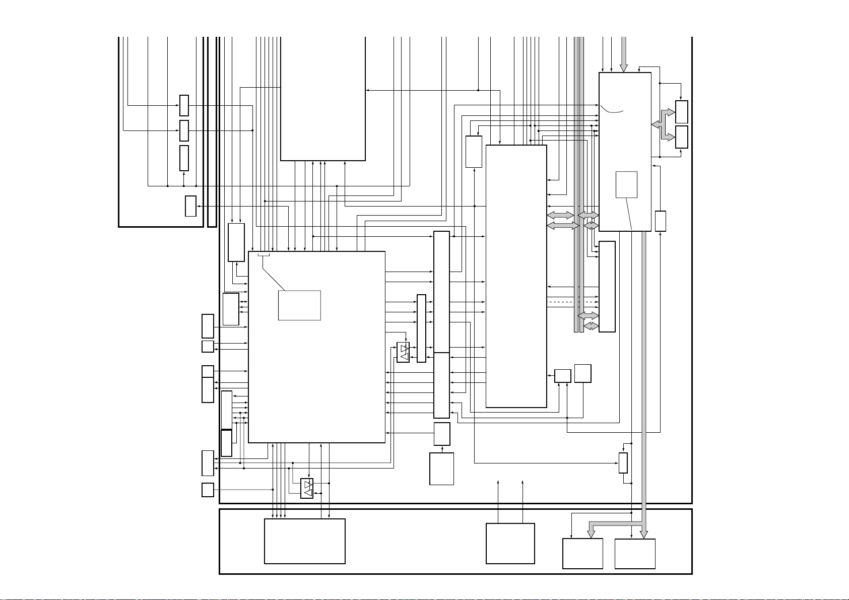
RGB Block Signal Flow
28
Inputs 1 or 2 from the I/O assy if RGB go directly to IC4603 (RGB A/D converter), if the signals are
component they enter IC4402 and then converted to RGB and sent to IC4603. After A/D
conversion takes place from IC4603 the now Digital 8-bit RGB is sent onto IC5001 & IC5102 the
interlace to progressive and selector IC’s. After I/P conversion the signals are sent out from
IC5001 as 2 channel 8-bit RGB through a selector switch and onto IC5301 the Digital Video
Processor IC. IC5301 contains the video correction circuitry needed to process the RGB signal.
Brightness, contrast, white balance, video enhance, screen size and on-screen display are all
controlled by IC5301. The output from the Video Process IC is 10-bit 2 channel RBG and exits
this assembly and enters the Digital Video Board.
Inputs 3 or 4 from the video card after conversion to Y/CB/CR (inside the video card) follow the
exact same path as the component flow for inputs 1 or 2.
The DVI input (input 5) from the video card is already 8-bit 2 channel digital RGB and bypasses
the RGB decode, A/D converter and I/P converter. The DVI signals directly enter the Digital Video
processor (IC5301).
Sync paths for all inputs enter IC4803 (sync processor) through various inputs. After sync
separation is preformed and analog to digital converting the sync outputs (for inputs 1, 2, 3 or 4)
is sent to the I/P select chip IC5001. The output from the I/P select chip is sent to a selector
switch. This switch will allow the RBG & sync or the DVI & sync to be sent onto the Digital Video
Process IC.
Sync signals are also sent to the system control IC (IC5505) to determine input signal frequency.
29
Digital video circuit block -
- - Digital video circuit block -
2ch 10bit RGB
R2 - D2
25-44 GA/B
4 - 22 BA/B
R3- D3
1 - 20 RA/B
22 CLK
24 DE
26 HD
28 VD
R3-D3
31 P.Mute
35/36 TX/RX
47 REM
36 PWR
compatible for HDE/MXE/Module.
Module CPU detect and set appropriate
D.Video assy
operation mode.
Sync
Data left
Data Right
Panel drv control CPU
Sub-field conv(Left)
Sub-field conv(Right)
DRV signal sequencer
D1- P2
10 Relay
12 AC-Off
13 PD_Trig
Data left
ADR PD
Data Right
DRV control
signals
DRV control
signals
PD det
disable PD
PD det
PWR ON
D1/5p
D1/1p
D1/6p
Vofs
compensation

Digital Video Assembly
30
The 2 phase 10 bit RGB signal, sync, data and clock lines input the
Digital Video Assembly from the RGB assembly. The signals pass
through the line buffer and into IC1301 and IC1410 (sub-field Data
Generators) where the address data is generated and sent out to the left
section and right section address connectors A-D.
X and Y drive sustain control is preformed by IC1703 and the panel
microcomputer IC1101. The panel microcomputer monitors the
horizontal and vertical drive signals to select the proper refresh rate. The
module microcomputer IC1207 controls the panel microcomputer via
logic lines sent through voltage logic level converters. IC1207 is
controlled by IC5505 the main microcomputer on the RGB board. IC1207
functions also include thermal sensor monitoring, dew detection, reset
control and is used not only to switch on the power supply but to also
switch off the power supply should one of the power down detect lines
activate.
 Loading...