Pioneer PDP-5030HD, PDP-4330HD Training Manual

Product Training Guide
Plasma Display Systems
PDP-5030HD & PDP-4330HD
Multimedia & Web Training Department
545 Nolan Drive Suite 100
Southlake, Texas 76092
Preface ……………………….…….. 3
System Configurations……………4-5
DVI Interface…………………..…….6
Contents
Front Panel Facilities..………………….25
Trap Switch….………………..……..7
Cell Structure………….…………….8
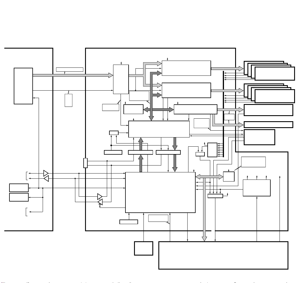
Overall Block………………..…9-11
Main PCB Layout………………12
Audio Amp……………………………13
Digital Video………………………...14-15
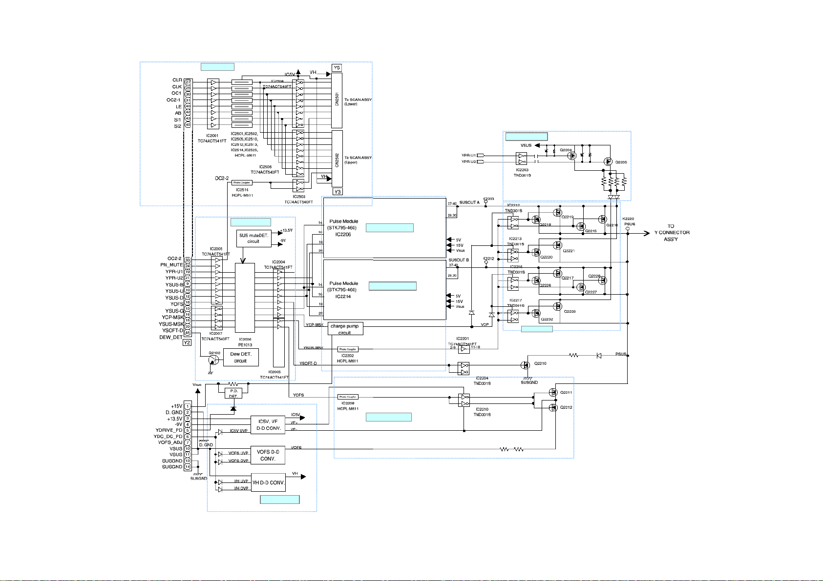
Y Drive…………………………….….16-17
X Drive…………………………….….18-19
Sub Address………………………...20-21
Resonance & Mid Clamp…….……22-23
MR Interface…………………………24
PCB Locations……………………..….…26
Disassembly……………………………...27-32
Factory Service Modes……………..….33-38
Adjustments……………………………..39-46
Shut Down & Power Down…….………47-53
Preface
3.
This technical training guide will address
the disassembly and adjustments of the
Pioneer PDP-5030HD & PDP4330HD Plasma
Display Systems.
This guide was designed as a servicing aid
and is not intended to replace the service
manual. The student should have the
appropriate service manual on hand when
when using this guide. Data in the service
manual for this unit contains specific
information on safety, parts and adjustments.
Safety information
Important safety data for this Pioneer model
is contained in the service manual. Before
returning the unit to the customer, complete
all product safety obligations and tests.
Technicians who bypass safety features or
fail to carry out safety checks may expose
themselves and others to possible injury,
and may be liable for any resulting damages.
For more information on electronic
circuits and block diagrams refer
to Service manuals ARP3107,
ARP3111 & ARP3113.
Lead in the solder used in this product
is a known reproductive toxicant which
may cause birth defects or other reproductive
harm. (California Health and Safety Code
Section 25249.5).
When servicing this or handling circuit
boards and other components which
contain solder, avoid unprotected skin
contact with the solder. Also, when
soldering do not inhale any smoke or
fumes produced.
3
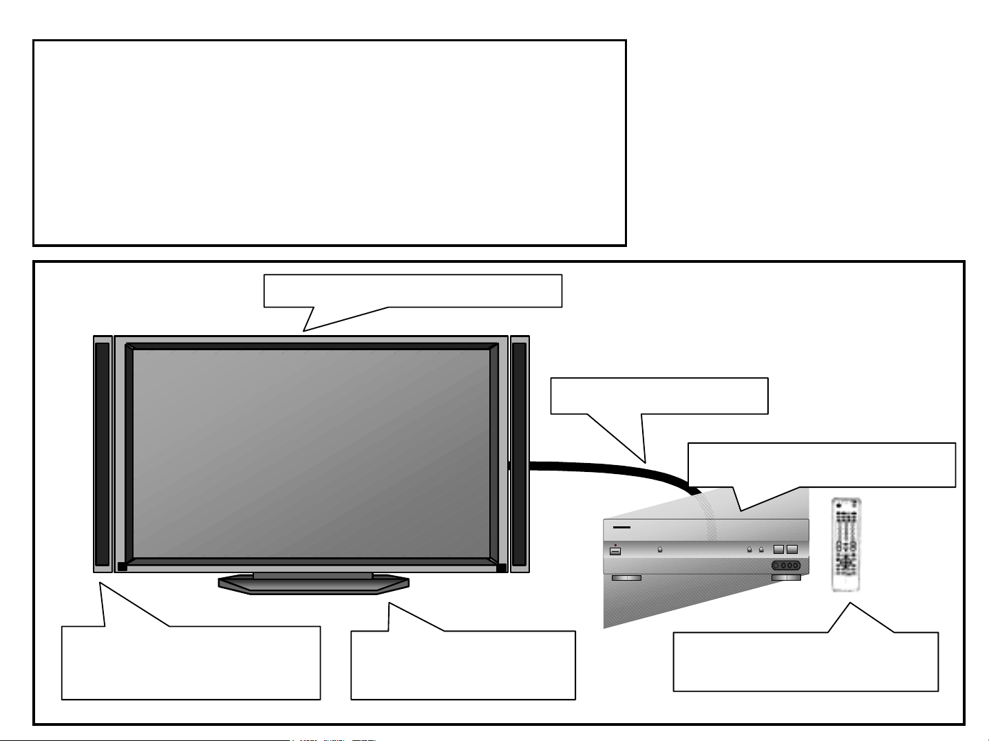
Model Number PDP-5030HD
p
t
System
Configuration
4.
Consists of 1 PDP-503PU (Plasma Dispay)
1 PDP-R03U (Media Receiver)
1 Remote (Packed with PDP-R03)
1 System Cable (3m long, Packed with PDP-R03U)
1 PDP-S06-LR (Pair of Side Mount Speaker)
1 PDK-TS01 (Table Top Stand)
tional Equipmen
O
50 inch
PDWB-5003 (Flat Wall Mount)
PWM-503 (Tilt Wall Mount)
PDP-503PU (Plasma Display)
50”
System Cable (3m)
PDP-R03U (Media Receiver)
STANDBY
POWER
STANDBY/ON
PLASMA DISPLAY SYSTEM
P L A S M A D ISPLAY SYSTEM
INPUT
+
-
UPDOWN
VOLUME
CHANNEL
PDP-S06-LR
(Side Mount Speaker / pair)
PDK-TS01
(Table Top Stand)
Remote
(Packed with PDP-R03U)
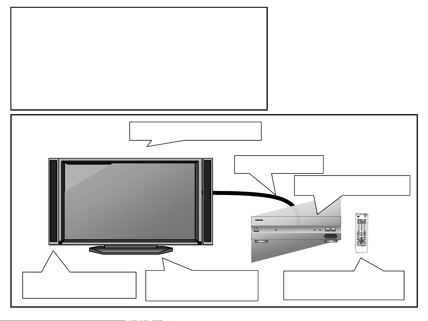
Model Number PDP-4330HD
p
t
System
Configuration
5.
Consists of 1 PDP-433PU (Plasma Dispay)
1 PDP-R03U (Media Receiver)
1 Remote (Packed with PDP-R03)
1 System Cable (3m long, Packed with PDP-R03U)
1 PDP-S09-LR (Pair of Side Mount Speaker)
1 PDK-TS01 (Table Top Stand)
O
tional Equipmen
43 inch
PDP-S08 (Under Mount Speaker)
PDWB-5003 (Flat Wall Mount)
PWM-503 (Tilt Wall Mount)
PDP-433PU (Plasma Display)
43”
System Cable (3m)
PDP-R03U (Media Receiver)
STANDBY
POWER
STANDBY/ON
P L A S M A D ISPLAY SYSTEM
P L A S M A D ISPLAY SYSTEM
INPUT
+
-
UPDOWN
VOLUME
CHANNEL
PDP-S09-LR
(Side Mount Speaker / pair)
PDK-TS01
(Table Top Stand)
Remote
(Packed with PDP-R03U)
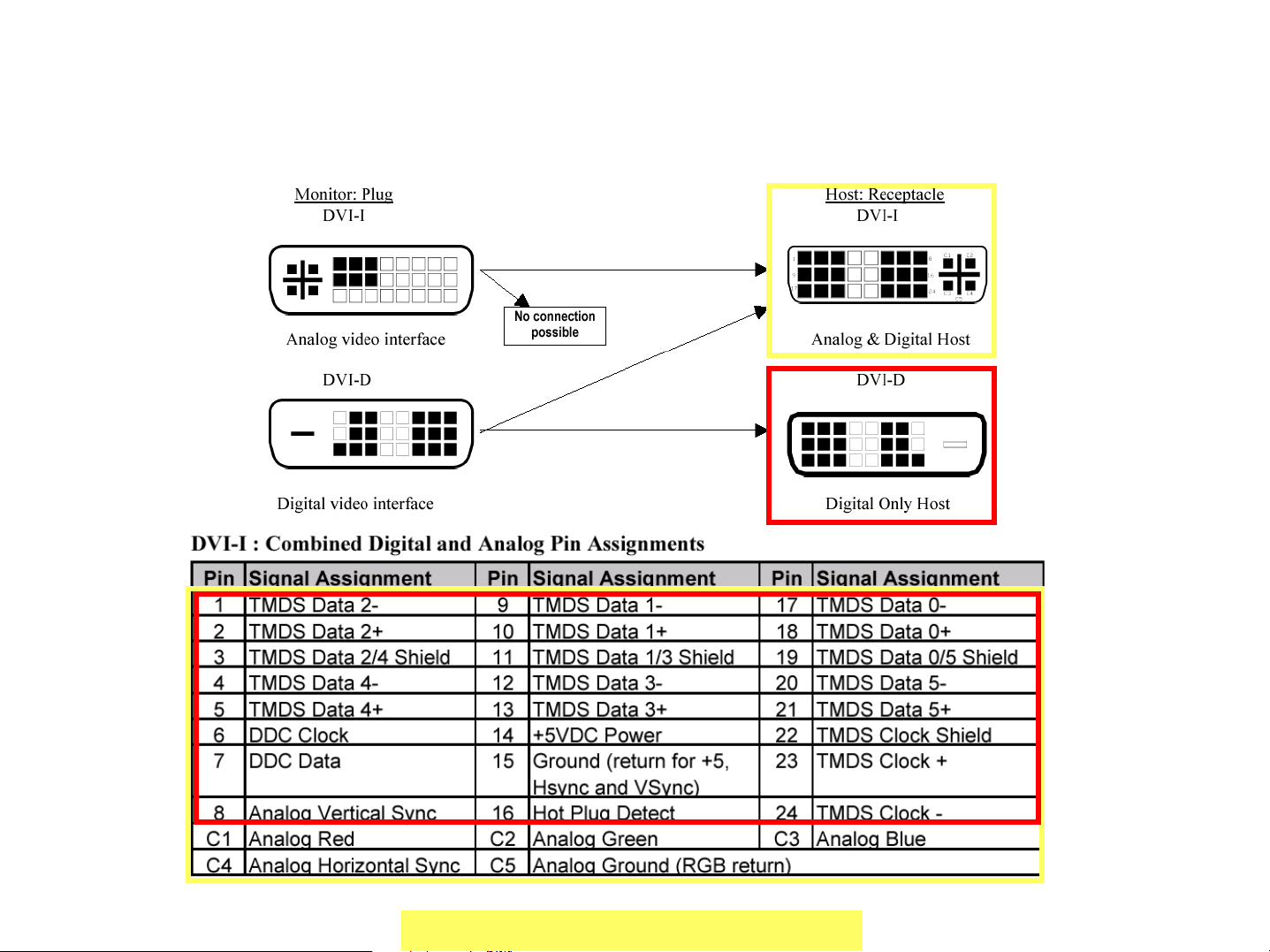
DVI-I interface for Plasma Display Systems
PDP-5030HD
PDP-4330HD
Media Receiver
PDP-R03U
Only!
HDCP System
No Connection
Possible
6.
There are two types of DVI interface; DVI-D and DVD-I.
(Yellow square)
Supplied cable must be used.
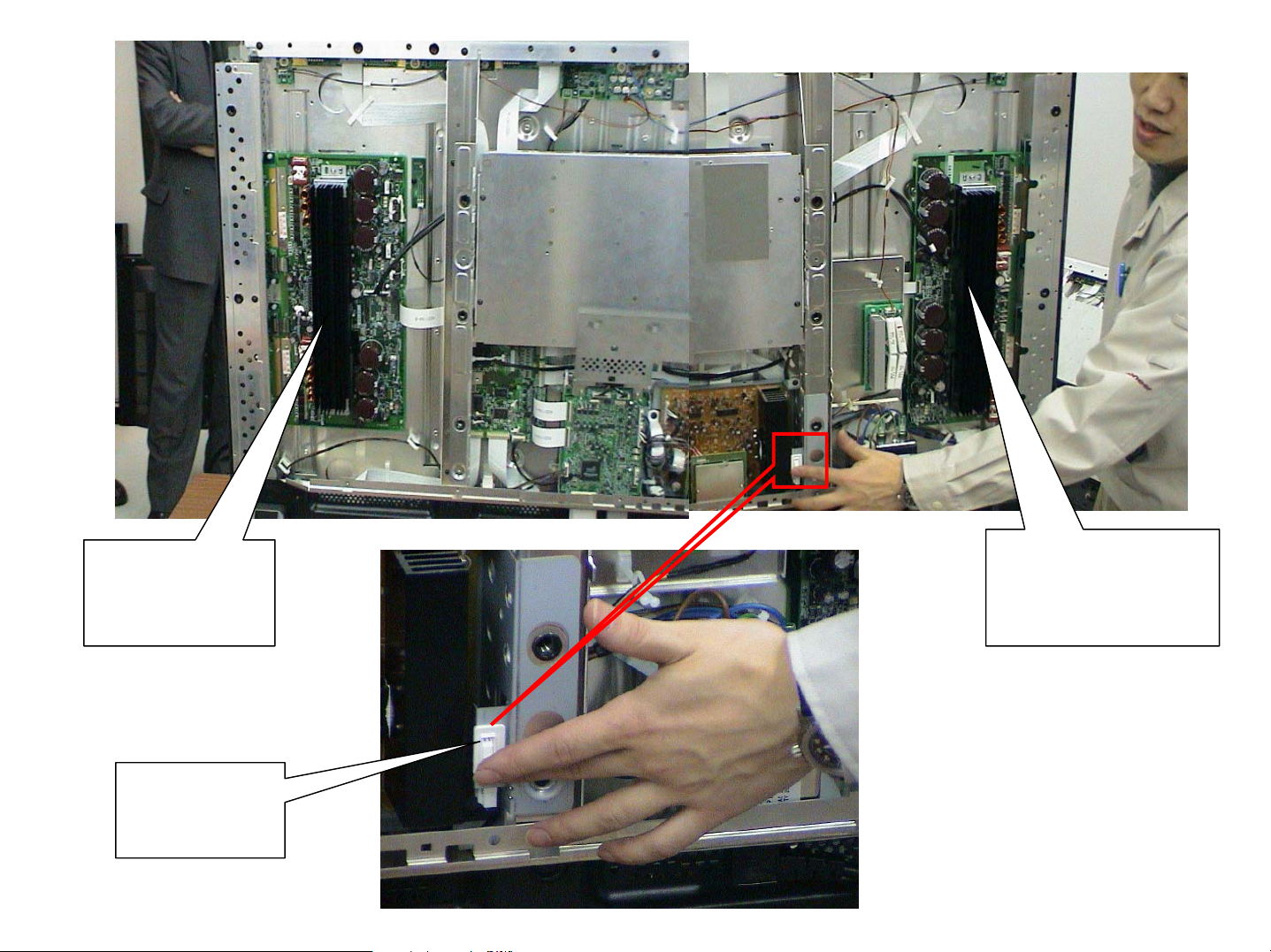
Y-Drive
Caution
Due to fan less
operation the X &
Y drive PCB's have
heat sinks attached
and must be
reinstalled if PCB
needs replacement.
Trap switch must be closed to
operate with back off.
Caution!
See Page 27 in this guide
or page 85 in the service manual.
7.
X-Drive
Heat Sink
AC Trap
Switch
Heat Sink
PDP-5030HD
PDP-4330HD
8.
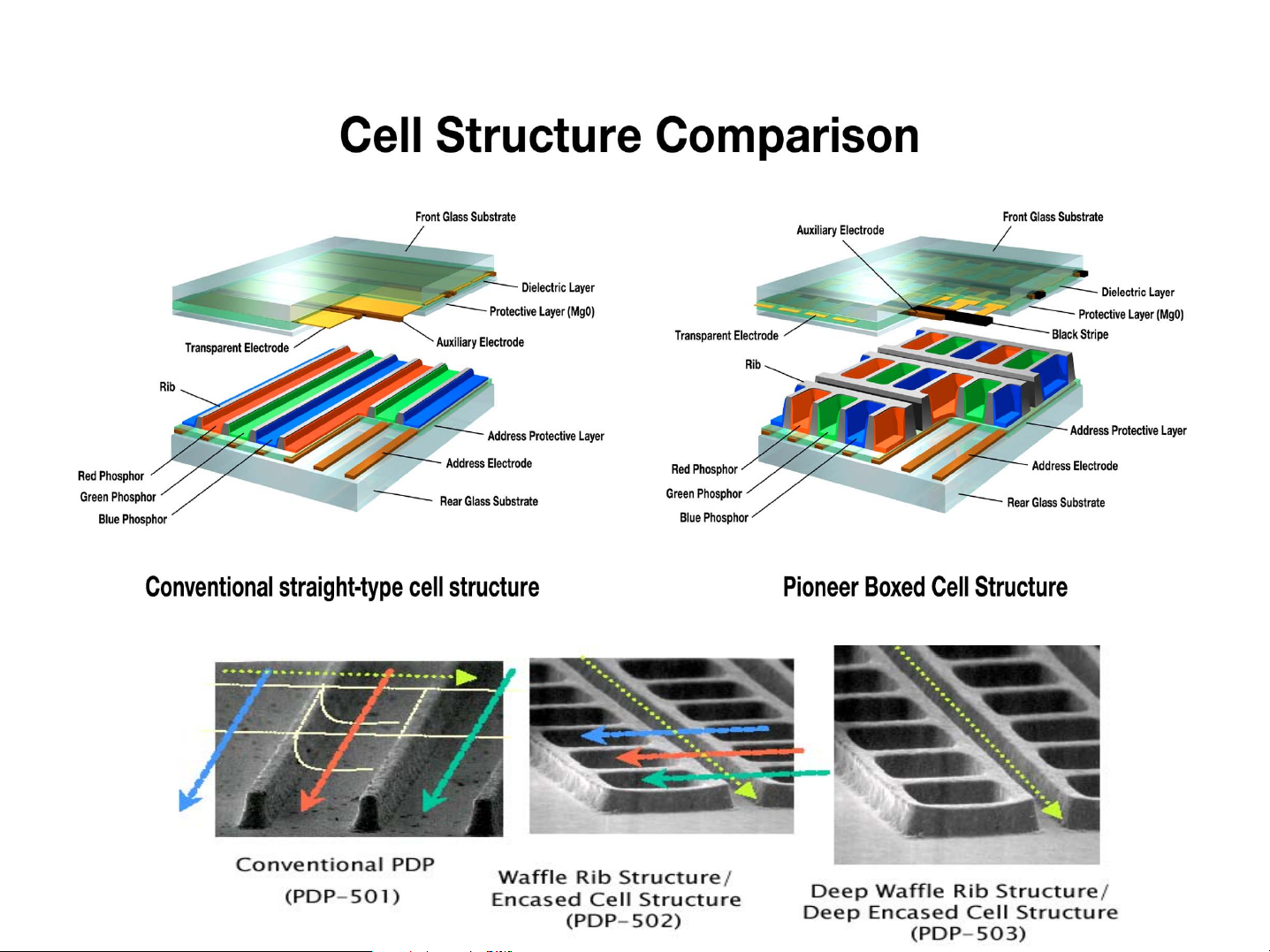
Higher luminance is realized by changing the cell structure.
2. Technical explanation on the new features.
2. Technical explanation on the new features.
- Higher luminance and contrast -
- Higher luminance and contrast -
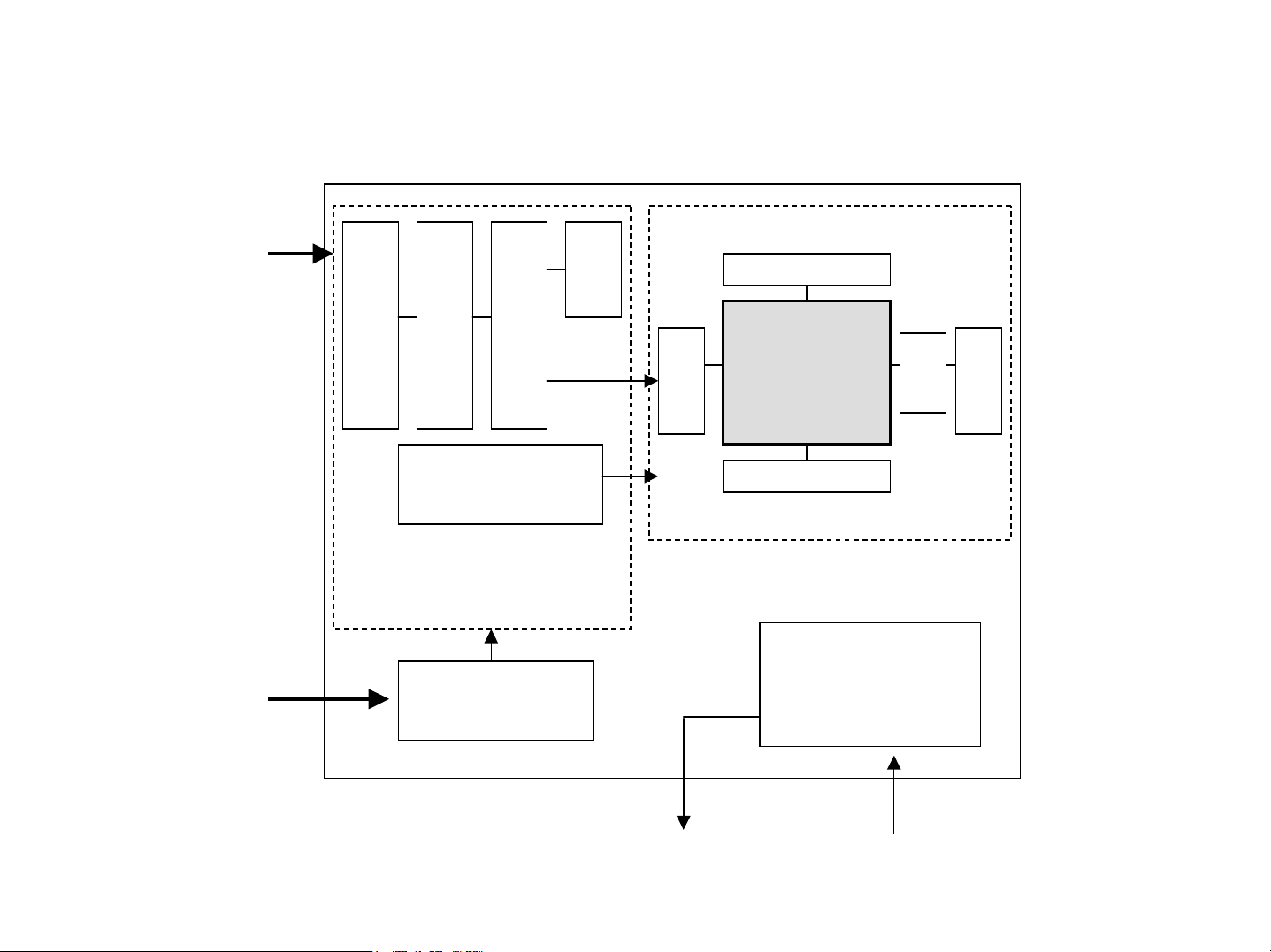
Overall Block diagram
Input From
Media
Receivers
DVI System
Connector
Input From
Media
Receivers
System
Connector
9.
R(A)0~7
G(A)0~7
B(A)0~7
R(B)0~7
G(B)0~7
B(B)0~7
CLK
HD
VD
DE
PDP
module
CONTROL
Data Interface
Data Controller
Drive controller
Panel controller
Memory Controller
Memory
X Drive
6V/15V
Address
PDP panel
Scan
Address
Power supply
Power On/Standby control
Y Drive
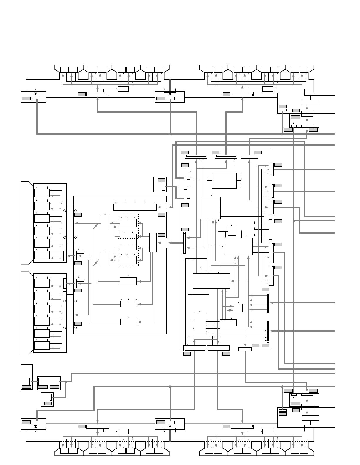
BLOCK DIAGRAM
10.
VADR2
CLA1
CLAMP A
ASSY
SCAN (B) ASSY
(UPPER)
SCAN (A) ASSY
(LOWER)
FRONT KEY
ASSY
ADR CONNECT A
ASSY
CLAMP
IC5
VCC_VH
IC6201
ADD
PSUS
SEL_PULSE
IC5
VCC_VH
IC6202
ADD
SEL_PULSE
IC5
VCC_VH
IC6203
ADD
SEL_PULSE
IC5
VCC_VH
IC6204
ADD
SEL_PULSE
IC5
VCC_VH
IC6205
ADD
SEL_PULSE
IC5
VCC_VH
IC6206
ADD
SEL_PULSE
SEL_PULSE
SEL_PULSE
SEL_PULSE
SEL_PULSE
SEL_PULSE
SEL_PULSE
FRONT KEY CONN
ASSY
IC5
IC6001
ADD
IC5
IC6002
ADD
IC5
IC6003
ADD
IC5
IC6004
ADD
IC5
IC6005
ADD
IC5
IC6006
ADD
VCC_VH
SCAN
VCC_VH
VCC_VH
VCC_VH
VCC_VH
VCC_VH
SCAN
PSUS
DriverICDriver
IC
DriverICDriver
AA1
Y DRIVE ASSY
Y4
PSUS
VCC_VH
V_IC5V
Y3
VCC_VH
V_IC5V
Y5
PSUS
Y6
IC
DriverICDriver
IC
CLK/LE
IC6501
Buffer IC
VC_VF+ VC_VF- V_OFS VCC_VH V_IC5V
DC/DC Conv.
VCP
Y-SUS
MASK
Block
VCP
Y-SUS
MASK
Block
Scan Signal
VC_VF+
Block
+5V +15V
VSUS
IC2206
Pulse Module
+15V VSUS
+Reset Block
+5V +15V VSUS
IC2204
Pulse Module
+15V
Soft-D
Block
VC_VF- V_OFS
Offset
Block
V_IC5V
Photo Coupler
Block
DriverICDriver
THERMAL
SENSOR
ASSY
Drive
Signal
Drive
Signal
IC
VADR2
BGA1
BRIDGE A
ASSY
TE1
Y1
Y2
Logic
Block
DriverICDriver
IC
VADR2
CLAMP
ADR CONNECT B
ASSY
AB1
D8 D9 D16
D1
+12V
V+5V_STB
+12V
DC/DC Conv.
V+3V
IC1703
XY Drive
Gen.
TXD/RX
Module
DIGITAL VIDEO
ASSY
KL_U0:2
XDRV_SIG
ADL_LE_UL
ADL_LE_DL
V+3V
X180
Clock
Gen.
IC1301 (IC31 L)
Sub-Field Conv.
for Left with Field Memory
V+3V
IC1101
Panel UCOM
+12V
D18
D6
Sequence Pattern
YDRV_SIG
SCAN_SIG
V+3V_I
V+2V_I
IC1401 (IC31 R)
Sub-Field Conv.
for Right with Field Memory
ADCLK_DR
V+5V_STB
IC1207
Module
UCOM
D13D12
DriverICDriver
IC
ADR RESONANCE
ASSY
V+5V
V+3V
V+2V
V+3V_IC
V+2V_IC
V+3V
IC1191
Flash
ROM
DriverICDriver
IC
CLK/LE
IC6601
Buffer IC
SUB ADDRESS A
ASSY
D10
D11
V+2V
V+3V
V+5V_STB
D15
D14
D2
BA2:9
BB2:9
GA2:9
GB2:9
RA2:9
RB2:9
TXD0/RX0
RE
LED_SIG
I2
D3D17
DriverICDriver
K2
K1
SAA3
+60
SAA1 SAA2
D7
D4
IC
VADR2
Q6706 - Q6711
VADR Gen.
ADR_CO
SW21 KL21 KL22
CLAMP B
ASSY
CLB1
IR (P)
ASSY
VADR2
RE1
CLAMP
ADR CONNECT D
ASSY
DriverICDriver
SUB ADDRESS B
ASSY
ADR RESONANCE
DriverICDriver
ASSY
IC
CLK/LE
IC6801
Buffer IC
DriverICDriver
BRIDGE C
ASSY
BGC1
IC
VADR2
CLAMP
VADR2
ADR CONNECT C
ASSY
DriverICDriver
IC
AC1
AD1
IC
DriverICDriver
IC
CLK/LE
IC6901
Buffer IC
DriverICDriver
DriverICDriver
IC
SAB1 SAB2
+60
SAB3
K2
IC
DriverICDriver
K1
ADR_CO
Q6706 - Q6711
VADR Gen.
VADR2
IC
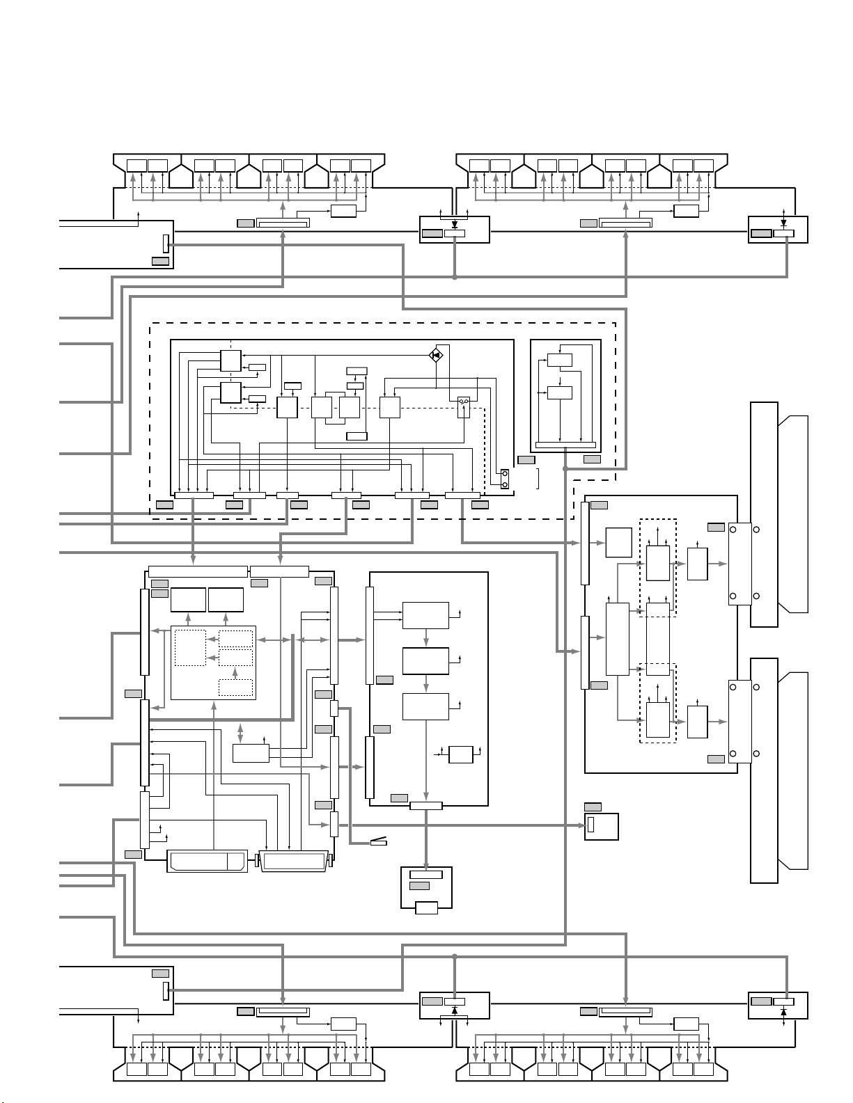
Note : When ordering service parts, be sure to refer to "EXPLODED VIEWS
11.
and PARTS LIST" or "PCB PARTS LIST".
DriverICDriver
VADR2
IC
DriverICDriver
IC
ADR CONNECT C
ASSY
AC1
DriverICDriver
CLK/LE
DriverICDriver
IC6801
Buffer IC
IC
IC
K3
SW POWER SUPPLY MODULE
SW POWER SUPPLY Block
+13.5V
-9V
T101
Switching
+13.5V
+6.5V
+15V
+12V
STB5V
-9V
+6.5V
T102
+12V
Q115
Switching
Q117
STB5V
Switching
Q119
VADR
Switching
VSUS_CONT
+15V
M111
Q112
M114
STB5V
T105T105T104T103
LIVE
NEUTRAL
SECONDARY
+13.5V
P1 P2 P5 P6 P3 P4
AUDIO AMP ASSY
R23
L
R
FOCUS
SRS
R27
R24
R11
AUDIO_SIG (L/R)
A24
A21
TRAP SW
L
R
Volume & Tone
A22
R3
R22
R21
R2
KEY1
KEY2
EEPROM
(HDCP KEY)
• Scalling
• Gamma
TMDS Receiver
V+5V_ST
V+5V_ST
IC4203
IC4204
(Sil861)
IC4201
EEPROM
(EDID)
I2C
Interface
Copy Guard
Release
TMDS
Receiver
I2C_BUS (SCL/SDA)
IC4011
I/O Expander
LED_SIG
TXD/RXD
SR_UP
SR_DW
TMDS with HDCP
R26
MR INTERFACE
ASSY
V+5V_DIG
System Cable Connector
VADR2
BGB1
BRIDGE B
ASSY
RC101
PRIMARY
POWER (RELAY)
VSUS
-9V
IC5202
& Balance
L, R
IC5201
SRS & Focus
L, R
IC5002
Power Amp.
L, R
L, R
SP21
SP OUT
DriverICDriver
VADR2
CLAMP
RL101
+15V
VSUS
+12V
+12V
+15V
+12V+13.5V
IC5001
Reg.
SP TERMINAL
ASSY
IC
ADR CONNECT D
ASSY
V MID CLAMP Block
P7
LIVE
NEUTRAL
DriverICDriver
IC
CLAMP
CLAMP
AC IN
DriverICDriver
AD1
VM1
X DRIVE ASSY
X1
DC/DC
Conv.
Block
Drive
Signal
+5V
Logic
Block
X2
Drive
Signal
L1
LED
ASSY
VSUS
CLK/LE
+5V
IC3200
Pulse
Module
+Reset
Pulse
Block
+5V
IC3201
Pulse
Module
+15V
+15VV_RN
+15VVSUS
DriverICDriver
IC6901
Buffer IC
VCP
X_SUS
MASK
VCP
X_SUS
MASK
IC
VADR2
CLAMP
CLB1
CLAMP B
ASSY
X3
P_SUS
P_SUS
X CONNECTOR (A) ASSYX CONNECTOR (B) ASSY
IC
X4
VADR2
DriverICDriver
K3
ADR CONNECT B
ASSY
IC
DriverICDriver
BRIDGE D
ASSY
BGD1
VADR2
CLAMP
VADR2
DriverICDriver
ADR CONNECT A
ASSY
IC
DriverICDriver
IC
AA1
DriverICDriver
IC6501
Buffer IC
CLK/LE
IC
DriverICDriver
IC
AB1
IC
DriverICDriver
IC
CLK/LE
IC6601
Buffer IC
DriverICDriver
IC
CLAMP A
ASSY
CLA1
CLAMP
VADR2
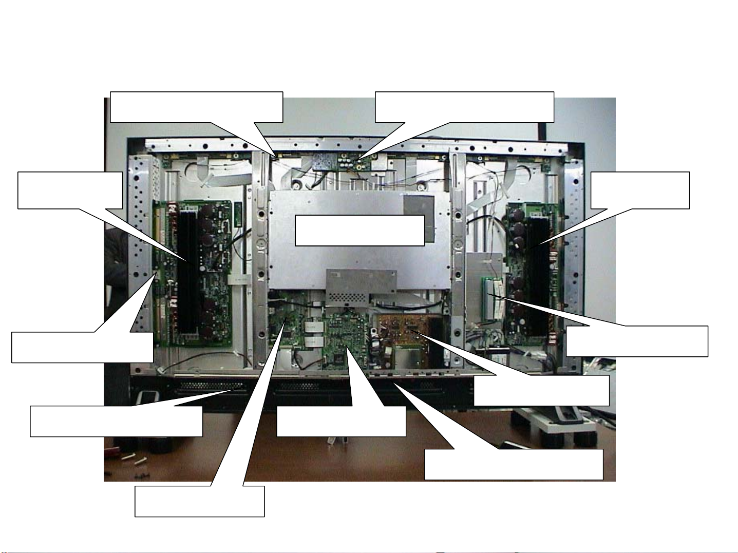
Main PCB Layout PDP-503PU & PDP-433PU
12.
Address Modules
Y-Drive X-Drive
Power Supply
Scan Modules
Resonance Assy
V-Mid Clamp
Audio Amp
Address Modules
MR Interface
Resonance Assy
Digital Video
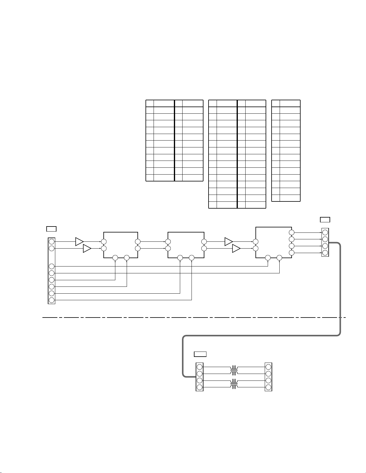
AUDIO AMP and SP TERMINAL ASSYS
12 watt X 2
Audio Amp
IC
13.
AUDIO AMP ASSY
PDP-433PU
No. Voltage (V) No. Voltage (V)
1 5.9 12 5.25
2 0 13 1.73
3 5.95 14 5.95
4 5.94 15 5.92
5 5.98 16 5.91
6 6.02 17 5.93
7 6.02 18 5.92
8 7.38 19 5.94
9 5.95 20 5.95
10 1.55 21 11.91
11 5.24 22 5.9
IC5201 (NJM2193L)IC5202 (CXA2021S) IC5002 (LA4628)
No. Voltage (V) No. Voltage (V)
1 5.95 16 11.91
25.9417 0
35.8418 0
4 5.98 19 5.98
5 5.98 20 5.91
6 5.97 21 5.97
7 5.98 22 5.98
8 5.98 23 5.98
9 5.98 24 5.98
10 5.97 25 5.97
11 5.97 26 5.98
12 5.98 27 5.98
13 5.96 28 5.84
14 5.98 29 5.94
150305.95
No. Voltage (V)
11.6
27.5
30
4 3.37
5 2.29
61.6
7 1.97
87.3
97.3
10 0
11 7.3
12 0
13 7.3
14 15
A24
CN5001
L
4 22
R
STB SW
7
A_MUTE
8
SCL
11
SDA
12
FOCUS
13
SRS
14
SP TERMINAL ASSY
IC5202
(CXA2021S)
1
Audio Pre-Amp.
11 12
A22
J5003
R+
8
L
14
R
96
IC5201
30
(NJM2193L)
Focus & SRS
1
Audio Processor
L
19
R
12
1
6
IC5002
(LA4628)
Audio
Power Amp.
R–
9
L+
11
L–
13
2
3
5
6
17 18 4 5
SP21
CN5302 CN5301
2
3
5
6
L5301
ATF1206
R+
R–
L+
L–
L5352
ATF1206
4
3
SPEAKER
TERMINAL
1
2
DIGITAL VIDEO ASSY
Digital RGB
Sync & Clock Signals
14.
MR INTERFACE
ASSY
IC4204
SiI861
To
MR
IC4005
Expander
IC4011
Expander
To
AUDIO
Assy
RGB 2 phase 8 bit
VD
HD
DE
CLK
RXDO
TXDO
A_SCL, A_SDA
DIGITAL VIDEO ASSY
Reflesh-rate
Det.
AND
CN1201
EXT_RXD
EXT_TXD
RXDO
TXDO
WE_PN
3.3V
Line
Buffer
RESET
EXD RXD
EXD TXD
RESET
Address BUS
Data BUS
Control Signal
3.3V
IC1191
Flash ROM
3.3V
HD
VD
Reset IC
3.3V
2.5V
IC1301 (IC31 L)
IC1401 (IC31 R)
APLR
VD 31
IC1101
(HD64F2328VF)
Panel Microcomputer
3.3V → 5.0V5.0V → 3.3VReset IC
RST PU
(M30624FGAFP)
Module Microcomputer
PD_TRIGGER
TEMP1
RST2
IC1207
AC_OFF
(PD6358)
DRAM
(PD6358)
DRAM
3.3V
RXD
BUSY
REQ_PU
IC1703 (IC23)
(PE5064)
Address
Resonance
STOPB
Control
PC_VIDEO
ADR_K_EMG
AND
APD MUTE
STB5V
RELAY
5V
IIC BUS
Address Data
Address Data
OR
ADR PD
OR
Sustain
Control
ADR K PD D
ADR K PD U
STB5V
EEP
ROM
DCC_PD
5V
RESONANCE
Panel W/B ADJ.
Hour/Pulse meter
DEW DET
5V
Converter
ADR CONNECT A - D
Assy (Left section)
ADR CONNECT A - D
Assy (Right section)
Y DRIVE Assy
X DRIVE Assy
ADR
Assy
pn
3.3V
2.5V
DC/DC
Block
STB5V
THERMAL
SENSOR
Assy
DIG. ADR. PD
SW POWER SUPPLY Module
12V
STB5V

Digital Video Assembly
15.
The 2 phase 8 bit RGB signal, sync, data and clock lines input the
Digital Video Assembly from the MR Interface assembly. The signals pass
through the line buffer and into IC1301 and IC1410 (sub-field Data
Generators) where the address data is generated and sent out to the left
section and right section address connectors A-D.
X and Y drive sustain control is preformed by IC1703 and the panel
microcomputer IC1101. The panel microcomputer monitors the
horizontal and vertical drive signals to select the proper refresh rate. The
module microcomputer IC1207 controls the panel microcomputer via
logic lines sent through voltage logic level converters. IC1207 is
controlled by the main microcomputer inside the media receiver. IC1207
functions also include thermal sensor monitoring, dew detection, reset
control and is used not only to switch on the power supply but to also
switch off the power supply should one of the power down detect lines
activate.
16.
Y drive circuit block -
- - Y drive circuit block -
Scan logic
Reset pulse gene
Logic Block
Detect over current
Detect over current
over voltage of Vofs/
Vh/IC5V.
Sus pulse gen
Sus pulse gen
Sus mask Bloc k
of 15V or Vc p.
Voffset gene
D-D conv
 Loading...