Page 1
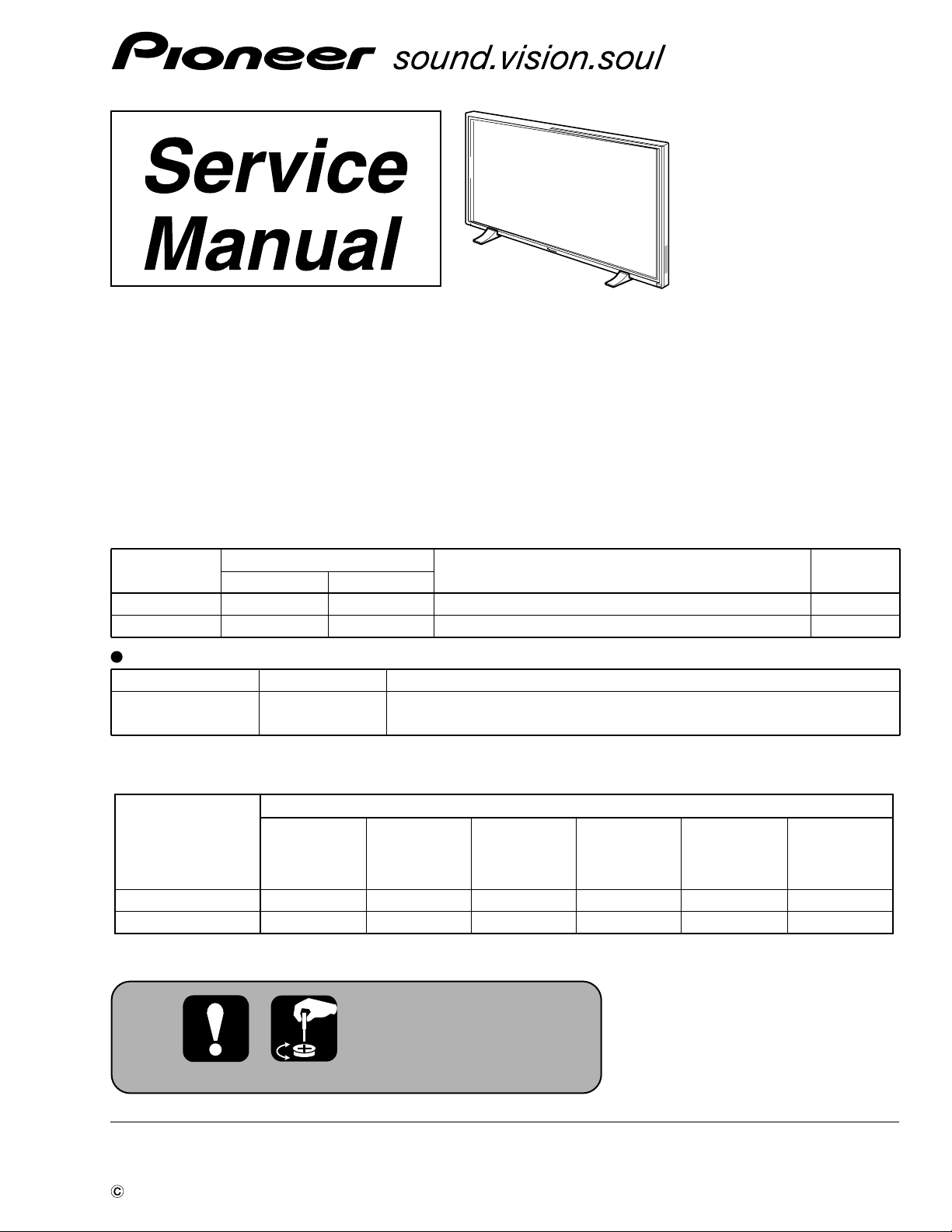
PDP-433CMX
PLASMA DISPLAY
PDP-433CMX
PDP-433MXE
THIS MANUAL IS APPLICABLE TO THE FOLLOWING MODEL(S) AND TYPE(S).
Type
LUCBW ? − AC100 - 120V
YVLDK − ? AC100 - 240V
PDP-433CMX PDP-433MXE
This Service Manual should be used together with the following manual(s).
Model No. Order No. Remarks
PDP-433CMX
PDP-433MXE
ARP3155
Model
EXPLODED VIEWS AND PARTS LIST, BLOCK DIAGRAM,
PCB PARTS LIST, IC INFOMATION, ADJUSTMENT, DIAGNOSIS, etc.
Power Requirement Remarks
ORDER NO.
ARP3156
The main parts having their serial numbers described in the table below are applicable to this service
manual. For details on replacing with the following parts, refer to Service Information for each part.
Part numbers and serial numbers of the main parts applicable to this service manual
Model No.
PDP-433CMX/LUCBW 002201 – 005131 – 004721 – 005011 – 006121 – 006811 –
PDP-433MXE/YVLDK 002201 – 005131 – 004721 – 005011 – 006121 – 006811 –
For details, refer to "Important symbols for good services".
PIONEER CORPORATION 4-1, Meguro 1-chome, Meguro-ku, Tokyo 153-8654, Japan
PIONEER ELECTRONICS (USA) INC. P.O. Box 1760, Long Beach, CA 90801-1760, U.S.A.
PIONEER EUROPE NV Haven 1087, Keetberglaan 1, 9120 Melsele, Belgium
PIONEER ELECTRONICS ASIACENTRE PTE. LTD. 253 Alexandra Road, #04-01, Singapore 159936
PIONEER CORPORATION 2003
SW POWER
SUPPLY
MODULE
(AXY1059)
Rear Case
(ANE1608)
RGB ASSY
(AWZ6744)
DIGITAL VIDEO
ASSY
(AWV1971)
X DRIVE ASSY
(AWV1985)
T – ZZR MAR. 2003 Printed in Japan
Y DRIVE ASSY
(AWZ6748)
Page 2
[ Important symbols for good services ]
In this manual, the symbols shown-below indicate that adjustments, settings or cleaning should be made securely.
When you find the procedures bearing any of the symbols, be sure to fulfill them:
1. Product safety
You should conform to the regulations governing the product (safety, radio and noise, and other regulations), and
should keep the safety during servicing by following the safety instructions described in this manual.
2. Adjustments
To keep the original performances of the product, optimum adjustments or specification confirmation is indispensable.
In accordance with the procedures or instructions described in this manual, adjustments should be performed.
3. Cleaning
For optical pickups, tape-deck heads, lenses and mirrors used in projection monitors, and other parts requiring cleaning,
proper cleaning should be performed to restore their performances.
4. Shipping mode and shipping screws
To protect the product from damages or failures that may be caused during transit, the shipping mode should be set or
the shipping screws should be installed before shipping out in accordance with this manual, if necessary.
5. Lubricants, glues, and replacement parts
Appropriately applying grease or glue can maintain the product performances. But improper lubrication or applying
glue may lead to failures or troubles in the product. By following the instructions in this manual, be sure to apply the
prescribed grease or glue to proper portions by the appropriate amount.For replacement parts or tools, the prescribed
ones should be used.
2
PDP-433CMX
Page 3

CONTENTS
3. SCHEMATIC DIAGRAM
3.1 OVERALL WIRING DIAGRAM(1/2)
3.2 OVERALL WIRING DIAGRAM(2/2)
3.3 SCAN (A) ASSY .................................................................................................................................... 26
3.4 SCAN (B) ASSY ...................................................................................................................................
3.5 X CONNECTOR A and B ASSYS
3.6 BRIDGE A - D ASSYS ........................................................................................................................... 35
3.7 ADR CONNECT A ASSY
3.8 ADR CONNECT B ASSY 38
3.9 ADR CONNECT C ASSY
3.10 ADR CONNECT D ASSY...................................................................................................................................... 42
3.11 ADR RESONANCE ASSY ...................................................................................................................................... 44
3.12 X DRIVE ASSY (1/3) .................................................................................................. ................................. 46
3.13 X DRIVE ASSY (2/3) ............................................................................................................................ 48
3.14 X DRIVE ASSY (3/3) ..................................................................................................................... 52
3.15 Y DRIVE ASSY (1/4) ............................................................................................................................
3.16 Y DRIVE ASSY (2/4) ............................................................................................................................ 56
3.17 Y DRIVE ASSY (3/4) ............................................................................................................................ 58
3.18 Y DRIVE ASSY (4/4) ............................................................................................................................ 60
3.19 SUB ADDRESS A ASSY ...................................................................................................................... 62
3.20 SUB ADDRESS B ASSY .................................................................................................................. 64
3.21 SLOT CONNECTOR ASSY ............................................................................................................... 66
3.22 DIGITAL VIDEO ASSY (1/10) ...............................................................................................................
3.23 DIGITAL VIDEO ASSY (2/10) ...
3.24 DIGITAL VIDEO ASSY (3/10) ............................................................................................................... 72
3.25 DIGITAL VIDEO ASSY (4/10) .................................................................................................................. 74
3.26 DIGITAL VIDEO ASSY (5/10) ......................................................................................................... 78
3.27 DIGITAL VIDEO ASSY (6/10) .............................................................................................................. 82
3.28 DIGITAL VIDEO ASSY (7/10) ..............................................................................................................
3.29 DIGITAL VIDEO ASSY (8/10)
3.30 DIGITAL VIDEO ASSY (9/10) 88
3.31 DIGITAL VIDEO ASSY (10/10).........................................................................................................................
3.32 I / O ASSY (1/2) ............................................................................................................................................................................................ .. 92
3.32 I / O ASSY (2/2) ..................................................................................................................................... 94
3.34 RGB ASSY (1/10) .................................................................................................................................................. 96
3.35 RGB ASSY (2/10) ...................................................................................................................................................... 98
3.36 RGB ASSY (3/10)..........................................................................................................................................................102
3.37 RGB ASSY (4/10).................................................................................................................................. 106
3.38 RGB ASSY (5/10)
3.39 RGB ASSY (6/10)
3.40 RGB ASSY (7/10)
3.41 RGB ASSY (8/10)
3.42 RGB ASSY (9/10)
3.43 RGB ASSY (10/10)
3.44 CONTROL, SP OUT L, MX LED, SIDE KEY, THERMAL SENSOR, KEY CONNECTOR, IR ASSYS
3.45 MX AUDIO ASSY
3.46 SW POWER SUPPLY MODULE(1/2)
3.47 SW POWER SUPPLY MODULE(2/2)
4. PCB CONNECTION DIAGRAM
4.1 ADR RESONANCE ASSY
4.2 SCAN A ASSY
4.3 SCAN B ASSY
4.4 X CONNECTOR A and B ASSYS
4.5 BRIDGE A - D ASSYS
4.6 ADR CONNECT A - D ASSYS
4.7 SUB ADDRESS A, B and SLOT CONNECTOR ASSYS
4.8 X DRIVE ASSY
4.9 Y DRIVE ASSY
4.10 DIGITAL VIDEO ASSY
4.11 I / O ASSY
4.12 RGB ASSY
4.13 CONTROL, SP OUT L, SP OUT R, THERMAL SENSOR and IR ASSYS
4.14 SIDE KEY, CONNECTOR, MX LED and MX AUDIO ASSYS
.............................................................................................................................................
..................................................................................................................................
........................................................................................................................
........................................................................................................................
...........................................................................................................
...............................................................................................................................................110
.................................................................................................................................
.................................................................................................................................
.................................................................................................................................
.................................................................................................................................
.................................................................................................................................
.................................................................................................................................
....................................................................................................................
.......................................................................................................................
........................................................................................................................................
........................................................................................................................................
............................................................................................................................
........................................................................................................................................
........................................................................................................................................
..........................................................................................................................
............................................................................................................................................
.........................................................................................................
.........................................................................................................
..........................................................................................................
......................... 40
...............................................................................................................
..............................................................................................................
..............................................................................................................
............................
............................
...................................................................................................
...................................................................................................
...........................................................................................................
...............................................................................................................
........................................................................
..............................................................
...........................................
.......
......
...
4
4
6
30
34
36
54
68
70
84
86
90
114
116
120
122
124
126
128
130
132
133
133
134
135
136
137
138
139
140
144
146
150
152
156
158
PDP-433CMX
3
Page 4
1
A
23
3. SCHEMATIC DIAGRAM
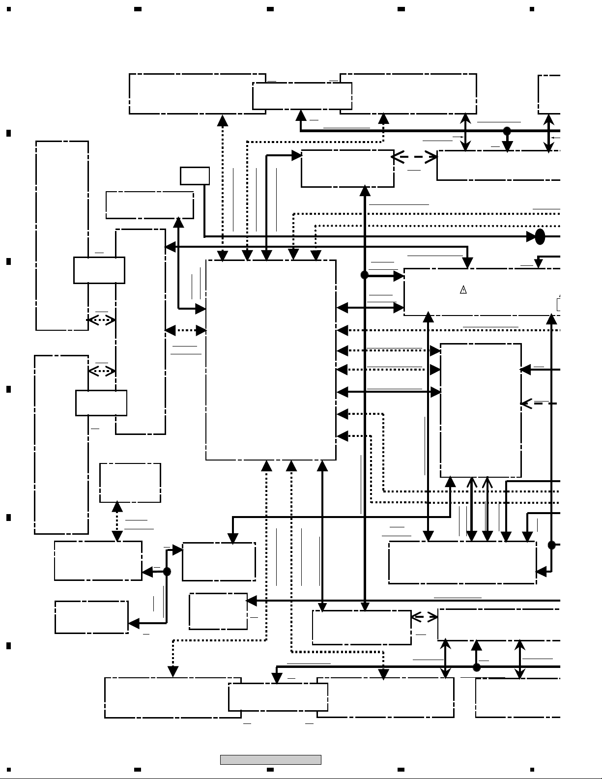
3.1 OVERALL WIRING DIAGRAM (1/2)
A
ADR CONNECT A
AWZ6678
FAN
B
SCAN A
AWZ6724
HOT PLATE
SA2
C
SA1
SB1
HOT PLATE
SB2
D
SCAN B
AWZ6725
KEY CONNECTOR
AWZ6695
E
IR
AWZ6643
(1)
ANG2469
(15)
(15)
ANG2469
(1)
SW1
KL1
THERMAL SENSOR
AWZ6696
Y1
Y4
Y DRIVE
AWZ6748
Y3
Y2
Y5
Y6
SIDE KEY
AWZ6637
J213(8)
ADD1195-
(6)
(4)
KL2
J113
ADX2778-
RE1
(3)
TE1
J110(3)
J203(50)
ADD1198-
C3 C1
ADX2741-
D18
D6
CONTROL
AWZ6633
SP OUT R
AWZ6706
(1) (1)
BRIDGE A BGA3
AWZ6728
BGA1
(4)
AA1
AA
BGA2
SAA2
J205(55) ADD1202-
J206(55) ADD1200-
J108(8) ADX2740-J212(55) ADD1201-
D8 D9 D16 D10 D11
DIGITAL VIDEO
AWV1971
J211(55) ADD1199-
PR1
(3)
AB2
J116 ADX2783-
SUB ADDRESS A
AWZ6692
SAA1
D1
D7
D2
D3
D4
D15
D14
D17D12 D13
J102(3) ADX2738-
J109 ADX2787-
SAB2
SAB1
SUB ADDRESS B
AWZ6693
ADR CONNECT B
AWZ6679
AB1 AB3
CONTACT
SAA3
J102(3) ADX2738-
J102(5)
ADX2738-
(23)
J102(15) ADX2738-
K1
P5
J119(13)
ADX2768-
P2 P1
J201(50)ADD1183-
J202(50)ADD1183-
J107(12)ADX2702-
J101(12) ADX2771-
J109
ADX2787-
SAB3
T1 T3 T4 T2 T5
J109 ADX2787-
K1
(23)
4
J116 ADX2783-
(4)
K4
P3
SW POWER SUPPLY
J204(30) ADD1207-
R2
R3
R4
RGB
AWZ6744
R9 R6 R7
ADX2706-
J5203(10)
I/O
AWZ6631
ADR RESONANCE
K5 K4
K2
K2
ADR RESONANCE
AWZ6751
AXY1059
R8
R1
J5204(10)
ADX2781-
AWZ6751
(10)
T6
AC2
K5
J207(55)
VM1
P6
(30)
(120)
J104 ADX2786-
(15)
J117 ADX2783-
AD1
ADR CONNECT D
F
AWZ6681
4
BGC3 BGC2
AD2
(1) (1)
PDP-433CMX
(4) J117 ADX2783-
BGC1
BRIDGE C
AWZ6730
AC3
AC1
ADR CONNECT C
AWZ6680
CONTACT
AC2
(4)
CONTACT
AB3
ADR CONNEC
AWZ6679
1234
Page 5
5
6
O
678
Note: When ordering service parts, be sure to refer to "EXPLODED VIEWS AND PARTS LIST"
or "PCB PARTS LIST".
For "EXPLODED VIEWS AND PARTS LIST" and "PCB PARTS LIST", refer to the service
manual ARP3155 for PDP-433CMX/LUCBW.
(1)(1)
AD2
BGB3BGB2
(4)
ADR CONNECT D
AWZ6681
AD1
ADX2783-
AC2
ADR CONNECT C
AWZ6680
AC1
AC3
BRIDGE B
AWZ6729
BGB1
A
J116 ADX2783-
J118 ADX2763-
J208(55) ADD1205-
J115(3) ADX2780-
J103(13) ADX2779-
J105(2) ADX2692-
AWZ6634
J118
ADX2763-
X
CONNECTOR
FAN
(1)
HOT PLATE
X3
ANG2469
X1
X2
X DRIVE
AWV1930
X4
(1)
HOT PLATE
ANG2469
J115(3)
ADX2780-
A5
A1
A6 A7
MX AUDIO
AWZ6644
A3
(6)
A
AWZ6726
EA1
EB1
B
C
(120)
K5
P6
FUSE
CONTACT
K3
(5)
J118 ADX2763-
P4
P7
J111 ADX2788-
SLOT CONNECTOR
S2
S1 S3
(4)
K2
R RESONANCE
AWZ6751
(10)
WER SUPPLY
1059
ADD1207-
R8
R1
4
J207(55) ADD1208-
VM1
(30)
7
ADX2781-
4T2 T5
T6
RESONANCE
WZ6751
K4
CONTACT
2783-
AB3
ADR CONNECT B
AWZ6679
(15)
J104 ADX2786-
J112(13 ADX2784-
K3
(5)
J117 ADX2783-
AB1
AB2
(120)
V1
VIDEO SLOT
AWV1906-
J209(55)ADD1206-
ADD1204-
J210(55)
J104 ADX2786-
J111 ADX2788-
J118 ADX2763-
(4)
BGD3 BGD2
BGD1
BRIDGE D
AWZ6731
(1) (1)
MAIN SW
J118 ADX2763-
J106(2)
INLET FILTER
AA1
ADR CONNECT A
AA3 AWZ6678
MS1
MS2
IN1
ADX2693-
IN2
ADX2709-
(3)
J114(1)
(10)
MX LED
AWZ6642
L1
(8)
SPL1
J109 ADX2787-
(6)
SP OUT L
AWZ6705
Wire rod connection
(Both ends housing)
Wire rod connection
(One side middle connection
connector)
Wire rod connection
(One side board inn connection)
FFC connection
Boad to Boad
Bridge Connector
X
CONNECTOR
B
AWZ6727
D
E
F
PDP-433CMX
5
6
7
8
5
Page 6
1
23
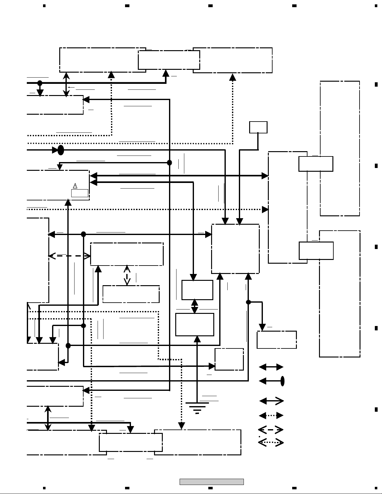
3.2 OVERALL WIRING DIAGRAM (2/2)
7 Connection Specifications of Each PCB
A
• SW POWER SUPPLY Module, MAIN SW and INLET Connection Specifications
<SW POWER SUPPLY Module Connection Specification>
CN num
P1 B12B-PH-K-S 1 +13.5V 1
B
P2 B13B-PH-K-S 1 +12V 1
C
P3
D
E
Part No. Pin
(JST) 2 GND 2
10 +5.0V_STB 10
11 GND_D 11
12 +12V 12
(JST) 2 +12V 2
10 POWER 10
11 NC 11
12 AC OFF 12
13 PD TRIGGER 13
53052-1510 1 +15V 1 KM250MA15 Y DRIVE Y1
10 V SUS 10
11 V SUS 11
12 NC 12
13 SUS_GND 13
14 SUS_GND 14
15 NC 15
Pin Name
3 -9.0V 3
4 GND 4
5 +6.5V 5
6 +6.5V 6
7 GND 7
8 GND 8
9 GND_STB 9
3 GND_D 3
4 GND_D 4
5 DIG-ADR PD 5
6 +5.0V_STB 6
7 GND_STB 7
8 SCL 8
9 SDA 9
2 GND_D 2
3 +13.5V 3
4 -9.0V 4
5 Y DRIVE PD 5
6 Y DCDC PD 6
7 VOFS_ADJ 7
8NC8
9NC9
to Pin Continuation
Connection by
wire rod
ADX2771-
(J101)
Connection by
wire rod
ADX2768-
(J119)
Connection by
wire rod
ADX2738-
(J102)
4
Connection Former
Part No.
KM200NA12 RGB I/O T1
(JST)
B13B-PH-SM3 DIGITAL VIDEO
(JST)
Connection
Former Assy
Connection
Former CN num.
(CN4003)
D1
(CN1901)
(CN2201)
F
6
PDP-433CMX
1234
Page 7
5
678
A
CN num
P4 53052-1310 1 +15V 1 KM250MA13 X DRIVE X1
P5 B5B-PH-K-S 1 V ADR 1 S3B-PH-SM3-TBB SUB ADDRESS A&B SAA2 (CN8801)
P6
P7 B2P3-VH 1 L 1 Main SW MS1
VM1 B10B-PH-K-S 1 SW_L 1 B5B-PH-SM3-TBB ADR RES
Part No. Pin
10 NC 10
11 SUS_GND 1 1
12 SUS_GND 1 2
13 NC 13
(JST) 2 V ADR 2 ADX2738- ×2 (JST)
Refer to the RGB I/O Assy connection specification
(JST) 2 N 2 ADX2692-
(JST) 2 D_GND_L 2 (J118) (JST)
10 V_ADR_U 5
Pin Name
2 GND_D 2 ADX2779-
3 X DRIVE PD 3 (J103)
4 X DCDC PD 4
5NC5
6NC6
7NC7
8 V SUS 8
9 V SUS 9
3 NC 3 (J102)
4 ADR_GND 4
5 ADR_GND 5
3 ADR_GND_L 3 ADX27634 V_MID_L 4
5 V_ADR_L 5
6 NC 1 B5B-PH-SM3-TBB ADR RES
7 NC 2 (J118) (JST)
8 ADR_GND_U 3 ADX2763-
9 V_MID_U 4
to Pin Continuation
Connection by wire rod
Connection by wire rod
Connect with branch
Connection by wire
rod (J105)
Connection by wire rod
Connection by wire rod
Connection
Former Part No.
1: VADR
2: N.C
3: ADR.GND
Connection
Former Assy
(Lower side)
(Uppewr side)
Connection
Former CN num.
(CN3101)
SAB2 (CN8901)
Pin arrangement
of SAA2 and SAB2
are common.
B
C
K3(D)
K3(U)
D
<MAIN SW Connection Specification>
CN num
SW1
SW2 1 L 1 −
Part No. Pin
Refer to the POWER SUPPLY Assy (above)
Pin Name
3
N
to Pin Continuation
Connection by wire rod
3 ADX2693-
(J106)
Connection
Former Part No.
<INLET Connection Specification>
CN num
IN1
IN2 1 INLET EARTH 1
Part No. Pin
Refer to the MAIN SW (above)
Pin Name
to Pin Continuation
Connection by wire rod
(ADX2709-)
(J114)
Connection
Former Part No.
PDP-433CMX
5
6
Connection
Former Assy
INLET IN1
Connection
Former Assy
−− −
Terminal Panel
7
Connection
Former CN num.
Connection
Former CN num.
8
E
F
7
Page 8
1
23
4
A
B
C
D
E
• DIGITAL VIDEO Assy Connection Specifications
CN num
D2 AKM1201- -TFB 1 GND_D 50 F FC AKM1201- -TFB RGB R2
(CN1003) 2 GND_D 49 ADD1183- (CN5701)
Part No. Pin
Refer to the POWER SUPPLY Assy connection specification
10 GB_RGB[8] 41
11 GA_RGB[7] 40
12 GB_RGB[7] 39
13 GA_RGB[6] 38
14 GB_RGB[6] 37
15 GA_RGB[5] 36
16 GB_RGB[5] 35
17 GA_RGB[4] 34
18 GB_RGB[4] 33
19 GA_RGB[3] 32
20 GB_RGB[3] 31
21 GA_RGB[2] 30
22 GB_RGB[2] 29
23 GA_RGB[1] 28
24 GB_RGB[1] 27
25 GA_RGB[0] 26
26 GB_RGB[0] 25
27 GND_D 24
28 GND_D 23
29 BA_RGB[9] 22
30 BB_RGB[9] 21
31 BA_RGB[8] 20
32 BB_RGB[8] 19
33 BA_RGB[7] 18
34 BB_RGB[7] 17
35 BA_RGB[6] 16
36 BB_RGB[6] 15
37 BA_RGB[5] 14
38 BB_RGB[5] 13
39 BA_RGB[4] 12
40 BB_RGB[4] 11
41 BA_RGB[3] 10
42 BB_RGB[3] 9
43 BA_RGB[2] 8
44 BB_RGB[2] 7
45 BA_RGB[1] 6
46 BB_RGB[1] 5
47 BA_RGB[0] 4
48 BB_RGB[0] 3
49 GND_D 2
50 GND_D 1
Pin Name
3 NC 48 (J201)
4NC47
5 GND_D 4 6
6 GND_D 4 5
7 GA_RGB[9] 44
8 GB_RGB[9] 43
9 GA_RGB[8] 42
to Pin Continuation
Connection Former
Part No.
Connection
Former Assy
Connection
Former CN num.
F
8
PDP-433CMX
1234
Page 9
5
678
A
CN num
D3
(CN1004) 2 GND_D 49 ADD1183- (CN5702)
Part No. Pin
AKM1201- -TFB
Pin Name
1 GND_D 5 0 F FC
3 − 48 (J202)
4 REM 47
5 − 46
6 RXD0/TXD0 45
7 − 44
8 TXD0/RXD0 43
9 − 42
10 − 41
11 − 40
12 − 39
13 MOD_SW 38
14 − 37
15 POWER 36
16 − 35
17 REQ_MD 34
18 − 33
19 PM_ST 32
20 PN_MUTE 31
21 − 30
22 GND_D 29
23 VD 28
24 GND_D 27
25 HD 26
26 GND_D 25
27 DE 24
28 GND_D 23
29 VCLK 2 2
30 GND_D 21
31 RA_RGB[9] 20
32 RB_RGB[9] 19
33 RA_RGB[8] 18
34 RB_RGB[8] 17
35 RA_RGB[7] 16
36 RB_RGB[7] 15
37 RA_RGB[6] 14
38 RB_RGB[6] 13
39 RA_RGB[5] 12
40 RB_RGB[5] 11
41 RA_RGB[4] 10
42 RB_RGB[4] 9
43 RA_RGB[3] 8
44 RB_RGB[3] 7
45 RA_RGB[2] 6
46 RB_RGB[2] 5
47 RA_RGB[1] 4
48 RB_RGB[1] 3
49 RA_RGB[0] 2
50 RB_RGB[0] 1
to Pin Continuation
Connection Former
Part No.
AKM1201- -TFB
Connection
Former Assy
RGB R3
Connection
Former CN num.
B
C
D
E
F
PDP-433CMX
5
6
7
8
9
Page 10
1
23
4
CN num
A
B
D4 B12B-PH-SM3-TBB 1 +3.3V_D 1 Connection by
(CN1001) (JST) 2 +3.3V_D 2
D6 AKM1201- -TFB 1 GND_D 50 F FC AKM1201- -TFB Y DRIVE Y2
(CN1701) 2 YRSV3 49 ADD1198- (CN2001)
C
D
E
F
Part No. Pin
10 GND_D 10
11 NC 11
12 GND_D 12
10 GND_D 41
11 SCAN_LE 40
12 SCAN_OC2_6 39
13 GND_D 38
14 SCAN_OC2_5 37
15 SCAN_OC2_4 36
16 GND_D 35
17 SCAN_OC2_3 34
18 SCAN_OC2_2 33
19 GND_D 32
20 SCAN_OC2_1 31
21 SCAN_OC1 30
22 GND_D 29
23 OE 28
24 SCAN_CLR 27
25 GND_D 26
26 SCAN_CLK 25
27 PN_MUTE 24
28 GND_D 23
29 YSOFT-D 22
30 YPR-U2 21
31 GND_D 20
32 YPR-U1 19
33 YOFS 18
34 GND_D 17
35 YCP-MSK 16
36 YSUS-MSK 15
37 GND_D 14
38 YSUS-G 13
39 YSUS-D 12
40 GND_D 11
41 YSUS-U 10
42 YSUS-B 9
43 GND_D 8
44 GND_D 7
45 GND_D 6
46 GND_D 5
47 +5.0V_D 4
48 +5.0V_D 3
49 +5.0V_D 2
50 +5.0V_D 1
Pin Name
3 +3.3V_D 3
4 GND_D 4
5 GND_D 5
6 GND_D 6
7 +2.5V_D 7
8 +2.5V_D 8
9 GND_D 9
3 YRSV2 48 (J203)
4 GND_D 4 7
5 DEW_DET 46
6 SCAN_SI2 45
7 GND_D 4 4
8 SCAN_SI1 43
9 SCAN_AB 42
to Pin Continuation
wire rod
ADX2702-
(J107)
Connection Former
Part No.
KM200NA12 RGB R4
(JST) (CN5704)
Connection
Former Assy
Connection
Former CN num.
10
1234
PDP-433CMX
Page 11
5
678
CN num
D7 KF050HA30L-TBB 1 GND_D 30 FF C KF050HA30L-TBB X DRIVE X2
(CN1702) 2 XRSV3 29 ADD1207- (CN3001)
Part No. Pin
Pin Name
3 GND_D 2 8 (J204)
4 XRSV2 27
5 GND_D 2 6
6 XRSV1 25
7 GND_D 2 4
8 PN_MUTE 23
9 GND_D 2 2
10 XNR-U 21
11 GND_D 20
12 XNR-D2 19
13 GND_D 18
14 XNR-D1 17
15 GND_D 16
16 XCP-MSK 15
17 GND_D 14
18 XSUS-MSK 13
19 GND_D 12
20 XSUS-G 11
21 GND_D 10
22 XSUS-D 9
23 GND_D 8
24 XSUS-U 7
25 GND_D 6
26 XSUS-B 5
27 GND_D 4
28 GND_D 3
29 +5.0V_D 2
30 +5.0V_D 1
to Pin Continuation
Connection Former
Part No.
Connection
Former Assy
Connection
Former CN num.
A
B
C
CN num
Part No.
Pin
Pin Name
to Pin Continuation
Connection Former
Part No.
Connection
Former Assy
Connection
Former CN num.
D16 B8B-PH-SM3-TBB 1 ADRK PD 1 ADX2740- S8B-PH-SM3-TBB SUB ADR A SAA2
(CN1503) (JST) 2 ADR_D 2 (J108) (JST) (CN8802)
D17 B8B-PH-SM3-TBB 3 ADR_U 3 ADX2787- S8B-PH-SM3-TBB SUB ADR B SAB2
(CN1603) (JST) 4 ADR_B 4 (J109) (JST) (CN8902)
5 GND_D 5
D16,D17 6 +12V 6 Connection by
Common use Common use7 ADRK EMG 7
wire rod
SAA2,SAB2
8 V MID SW 8
D18 B3B-PH-SM3-TBB 1 +5.0V_D 1 B3B-PH-SM3-TBB SENSOR TE1
(CN1203) (JST) 2 TEMP 2
3 GND_D 3
Connection by
wire rod
ADX2741-
(J110)
(JST) (CN8351)
D
E
F
PDP-433CMX
5
6
7
8
11
Page 12
1
23
4
A
B
C
D
E
CN num
D8
(CN1501)
D9 AKM1202- -TFB 3 GND_D 53 ADD1200- AKM1202- -TFB ADR CON B AB1 (Upper side)
(CN1502)
D10 AKM1202- -TFB 5 DATA_R_A1 51 ADD1208- AKM1202- -TFB ADR CON C AC1 (Upper side)
(CN1504)
D11 AKM1202- -TFB 7 DATA_B_A2 4 9 ADD1205- AKM1202- -TFB ADR CON D AD1 (Upper side)
(CN1505)
D8 - D 11 12 GND_D 44 AA1 - AD1
Common use Common use13 DATA_G_B1 43
Part No.
AKM1202- -TFB
Pin
Pin Name
1 ADR_PD 55 ADD1202-
2 DATA_B_A1 54
4 DATA_G_A1 5 2
6 GND_D 5 0
8 DATA_G_A2 4 8
9 GND_D 4 7
10 DATA_R_A2 46 All F FC
11 DATA_B_B1 45
14 DATA_R_B1 42
15 GND_D 41
16 DATA_B_B2 40
17 DATA_G_B2 3 9
18 GND_D 38
19 DATA_R_B2 37
20 DATA_B_C1 36
21 GND_D 35
22 DATA_G_C1 34
23 DATA_R_C1 3 3
24 GND_D 32
25 DATA_B_C2 31
26 DATA_G_C2 30
27 GND_D 29
28 DATA_R_C2 2 8
29 DATA_B_D1 27
30 GND_D 26
31 DATA_G_D1 25
32 DATA_R_D1 2 4
33 GND_D 23
34 DATA_B_D2 22
35 DATA_G_D2 21
36 GND_D 20
37 DATA_R_D2 1 9
38 DATA_B_E1 1 8
39 GND_D 17
40 DATA_G_E1 16
41 DATA_R_E1 15
42 GND_D 14
43 DATA_B_E2 1 3
44 DATA_G_E2 12
45 GND_D 11
46 DATA_R_E2 10
47 ADR_HZ 9
48 ADR_HBLK 8
49 +5.0V_D 7
50 +3.3V_D 6
51 GND_D 5
52 ADR_LBLK 4
53 ADR_LE 3
54 GND_D 2
55 ADR_CLK 1
to Pin Continuation
(J205) (Upper side)
(J206) (CN6551)
(J207) (CN6601)
(J208) (CN6651)
Connection Former
Part No.
AKM1202- -TFB
Connection
Former Assy
ADR CON A AA1 (Upper side)
(Upper side)
(Upper side)
(Upper side)
Connection
Former CN num.
(CN6501)
F
12
PDP-433CMX
1234
Page 13
5
678
CN num
D12
(CN1601)
D13 AKM1202- -TFB 3 GND_D 53 ADD1199- AKM1202- -TFB ADR CON C AC1 (Lower side)
(CN1602)
D14 AKM1202- -TFB 5 DATA_B_A1 5 1 ADD1204- AKM1202- -TFB ADR CON B AB1 (Lower side)
(CN1604)
D15 AKM1202- -TFB 7 DATA_R_A2 49 ADD1206- AKM1202- -TFB ADR CON A AA1 (Lower side)
(CN1605)
D12 - D15 12 GND_D 4 4 AA1 - AD1
Common use 13 DATA_G_B1 43 Common use
Part No.
AKM1202- -TFB
Pin
Pin Name
1 ADR_PD 55 ADD1201-
2 DATA_R_A1 54
4 DATA_G_A1 5 2
6 GND_D 5 0
8 DATA_G_A2 4 8
9 GND_D 4 7
10 DATA_B_A2 46 All F FC
11 DATA_R_B1 45
14 DATA_B_B1 42
15 GND_D 41
16 DATA_R_B2 40
17 DATA_G_B2 3 9
18 GND_D 38
19 DATA_B_B2 37
20 DATA_R_C1 3 6
21 GND_D 35
22 DATA_G_C1 34
23 DATA_B_C1 33
24 GND_D 32
25 DATA_R_C2 3 1
26 DATA_G_C2 30
27 GND_D 29
28 DATA_B_C2 28
29 DATA_R_D1 2 7
30 GND_D 26
31 DATA_G_D1 25
32 DATA_B_D1 24
33 GND_D 23
34 DATA_R_D2 2 2
35 DATA_G_D2 21
36 GND_D 20
37 DATA_B_D2 19
38 DATA_R_E1 18
39 GND_D 17
40 DATA_G_E1 16
41 DATA_B_E1 1 5
42 GND_D 14
43 DATA_R_E2 13
44 DATA_G_E2 12
45 GND_D 11
46 DATA_B_E2 1 0
47 ADR_HZ 9
48 ADR_HBLK 8
49 +5.0V_D 7
50 +3.3V_D 6
51 GND_D 5
52 ADR_LBLK 4
53 ADR_LE 3
54 GND_D 2
55 ADR_CLK 1
to Pin Continuation
(J212)
(J211) (CN6601)
(J210) (CN6551)
(J209) (CN6501)
Connection Former
Part No.
AKM1202- -TFB
Connection
Former Assy
ADR CON D AD1 (Lower side)
(Lower side)
(Lower side)
(Lower side)
(Lower side)
Connection
Former CN num.
(CN6651)
A
B
C
D
E
F
PDP-433CMX
5
6
7
8
13
Page 14
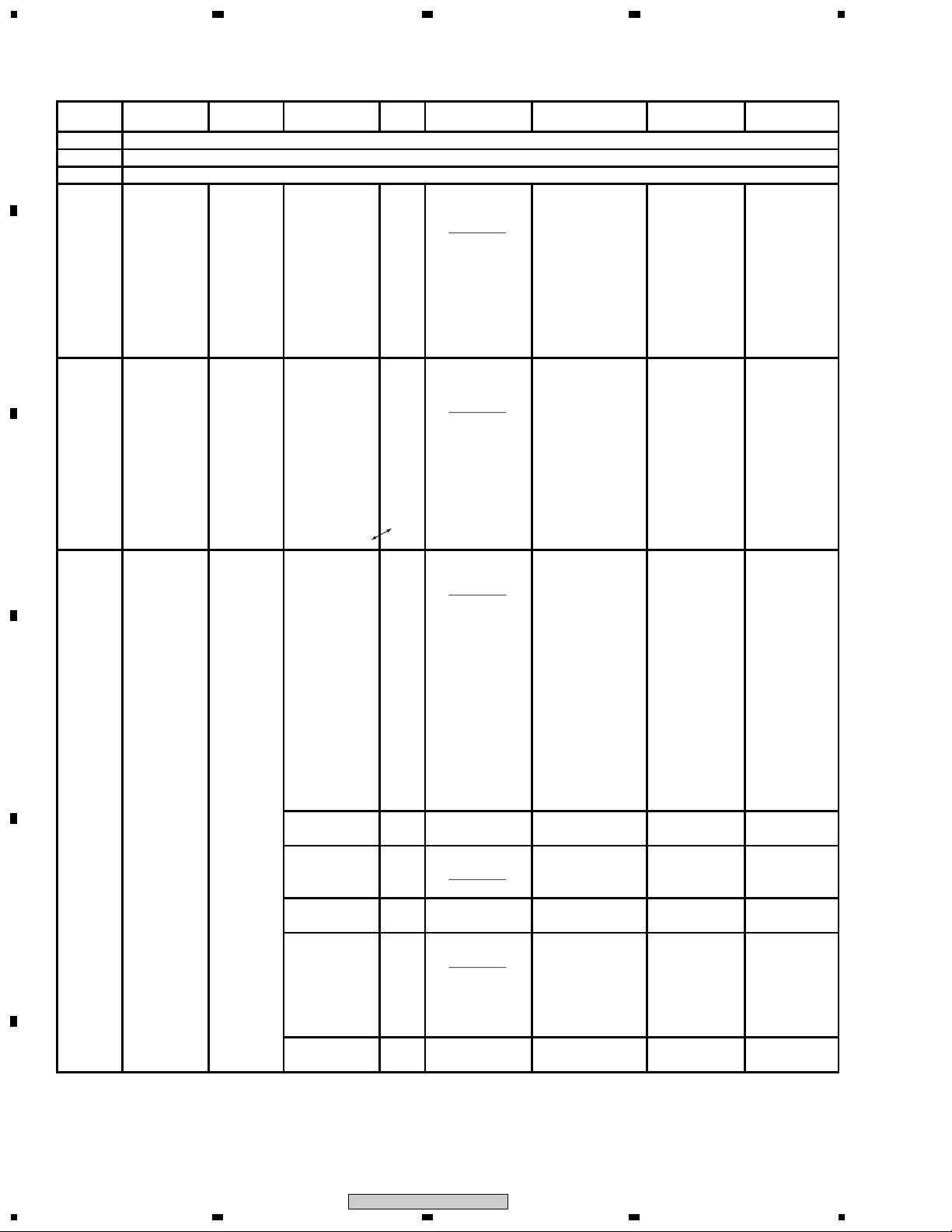
1
• RGB Assy Connection Specification
<RGB Assy connection specification>
CN num
A
R1 AKM1203- 1 GND 1 Boad to Boad AKP1219- SLOT I/F S2
(CN5201) (KEL) 2 GND 2 (KEL) (CN8102)
B
C
D
E
F
Part No.
Pin
3 SIG1(Y) 3
4 GND 4
5 SIG2(CB) 5
6 GND 6
7 SIG3(CR) 7
8 GND 8
9 HD_PLD 9
10 GND 10
11 VD_PLD 11
12 GND 12
13 NC 13
14 GND 14
15 NC 15
16 GND 16
17 SLOT_ST 17
18 SDIN_SEL 18
19 FUT3 19
20 FUT2 20
21 NC 21
22 NC 22
23 VD_PLKU 23
24 GND 24
25 HD_PLKU 2 5
26 GND 26
27 VD_PLK 27
28 GND 28
29 HD_PLK 2 9
30 GND 30
31 GND 31
32 RB_PLK0 32
33 RB_PLK1 33
34 RB_PLK2 34
35 RB_PLK3 35
36 RB_PLK4 36
37 RB_PLK5 37
38 RB_PLK6 38
39 RB_PLK7 39
40 GND 40
41 GND 41
42 GB_PLK0 42
43 GB_PLK1 43
44 GB_PLK2 44
45 GB_PLK3 45
46 GB_PLK4 46
47 GB_PLK5 47
48 GB_PLK6 48
49 GB_PLK7 49
50 GND 50
51 GND 51
52 BB_PLK0 52
53 BB_PLK1 53
54 BB_PLK2 54
55 BB_PLK3 55
56 BB_PLK4 56
57 BB_PLK5 57
58 BB_PLK6 58
59 BB_PLK7 59
60 GND 60
23
Pin Name
to Pin Continuation
Connection Former
Part No.
Connection
Former Assy
4
Connection
Former CN num.
14
1234
PDP-433CMX
Page 15
5
678
CN num
Part No.
Pin
61 GND 61
62 GND 62
63 SCL 63
64 GND 64
65 SDA 65
66 GND 66
67 GND 67
68 GND 68
69 NC 69
70 GND 70
71 NC 71
72 GND 72
73 +5.0V_STB 73
74 GND 74
75 NC 75
76 NC 76
77 IN4DET 7 7
78 IN3DET 7 8
79 SLOT_ST2 79
80 SRIN 80
81 NC 81
82 NC 82
83 GND 83
84 GND 84
85 SCDT3 85
86 GND 86
87 DE_PLK 87
88 GND 88
89 CLK_PLK 89
90 GND 90
91 GND 91
92 BA_PLK7 92
93 BA_PLK6 93
94 BA_PLK5 94
95 BA_PLK4 95
96 BA_PLK3 96
97 BA_PLK2 97
98 BA_PLK1 98
99 BA_PLK0 99
100 GND 100
101 GND 101
102 GA_PLK7 102
103 GA_PLK6 103
104 GA_PLK5 104
105 GA_PLK4 105
106 GA_PLK3 106
107 GA_PLK2 107
108 GA_PLK1 108
109 GA_PLK0 109
110 GND 110
111 GND 111
112 RA_PLK7 112
113 RA_PLK6 113
114 RA_PLK5 114
115 RA_PLK4 115
116 RA_PLK3 116
117 RA_PLK2 117
118 RA_PLK1 118
119 RA_PLK0 119
120 GND 120
Pin Name
to Pin Continuation
Connection Former
Part No.
Connection
Former Assy
Connection
Former CN num.
A
B
C
D
E
F
PDP-433CMX
5
6
7
8
15
Page 16
1
23
4
A
B
C
D
E
CN num
R2
R3
R4
R6 Boad in 1 G 1 Connection by
(J5203) 2 GND 2
R7 Boad in 1 GND 1 KM200NA10 RGB I/O T4
(J5204) 2 +9.0V_PIC 2
R8 B30B-KRWHK
(CN5202) (JST) GND_STB 2
Part No.
Pin
Refer to the DIGITAL VIDEO Assy connection specification
Refer to the DIGITAL VIDEO Assy connection specification
Refer to the DIGITAL VIDEO Assy connection specification
3B3
4 GND 4
5R5
6 GND 6
7 HD_RGB 7
8 GND 8
9 RGB_VD 9
10 GND 10
3 GND 3
4 +3.3V_PLD 4
5 GND 5
6 +3.3V_AD 6
7 GND 7
8 +5.0V_AD/RGB 8
9 GND 9
10 NC 10
11 -5.0V_AD/RGB −
1 (1 of column A)
2 (2 of column A)
3 (3 of column A)
4 (4 of column A)
5 (5 of column A)
6 (6 of column A)
7 (7 of column A)
8 (8 of column A)
9 (9 of column A)
10 (10 of column A)
11 (11 of column A)
12 (12 of column A)
13 (13 of column A)
14 (14 of column A)
15 (15 of column A)
16 (1 of column B)
17 (2 of column B)
18 (3 of column B)
19 (4 of column B)
20 (5 of column B)
21 (6 of column B)
22 (7 of column B)
23 (8 of column B)
24 (9 of column B)
25 (10 of column B)
26 (11 of column B)
27 (12 of column B)
28 (13 of column B)
29 (14 of column B)
30 (15 of column B)
Pin Name
IN1_VD 1 KM200NA15 RGB I/O T5
IN1_HD 3
GND_STB 4
IN1DET 5
A_MUTE2 6
A_MUTE1 7
EXT_INT 8
FIX_VAR 9
VOL 1 0
RGB_SEL 11
WP_SW 12
V+5V_STB 13
GND_STB 14
V+12V_PLD 15
NC −
NC −
*LED_G 1 S3B-PH-SM3-TBB MX LED L1
*LED_R 2 ADX2788- ( JST) (CN8501)
GND_STB 3 ( J111)
NC −
NC −
V+5.0V_AD/RGB 1 B6B-PH-SM3-TBB MX AUDIO A5
FAN 2 ADX2788- (JST) (CN8703)
FAN_NG 3 ( J111)
TEMP3 4
AUDIO_NG 5
GND_STB 6
NC −
NC −
to Pin Continuation
Boad in wire rod
ADX2706-
Connection by
Boad in wire rod
ADX2781-
Connection by
wire rod
ADX2788-
Connection by wire rod
Connection by wire rod
(J5203)
(J5204)
(J111)
Connection Former
Part No.
KM200NA10 RGB I/O T3
(JST) (CN4004)
(JST) (CN4005)
(JST) (CN4002)
Connection
Former Assy
Connection
Former CN num.
F
16
PDP-433CMX
1234
Page 17
1
234
CN num
R9 KM200NA8 1 CB_MUTE 1 Connection by
(CN5503) (JST) 2 REM_MP 2
Part No.
Pin
3 GND_STB 3
4 V+5.0V_STB 4
5 RXD1 5
6 TXD1 6
7 KEYSCAN 7
8NC8
Pin Name
to Pin Continuation
wire rod
ADX2787-
(J109)
Connection Former
Part No.
B8B-PH-SM3-TBB CONTROL C 1
(JST) (CN8006)
Connection
Former Assy
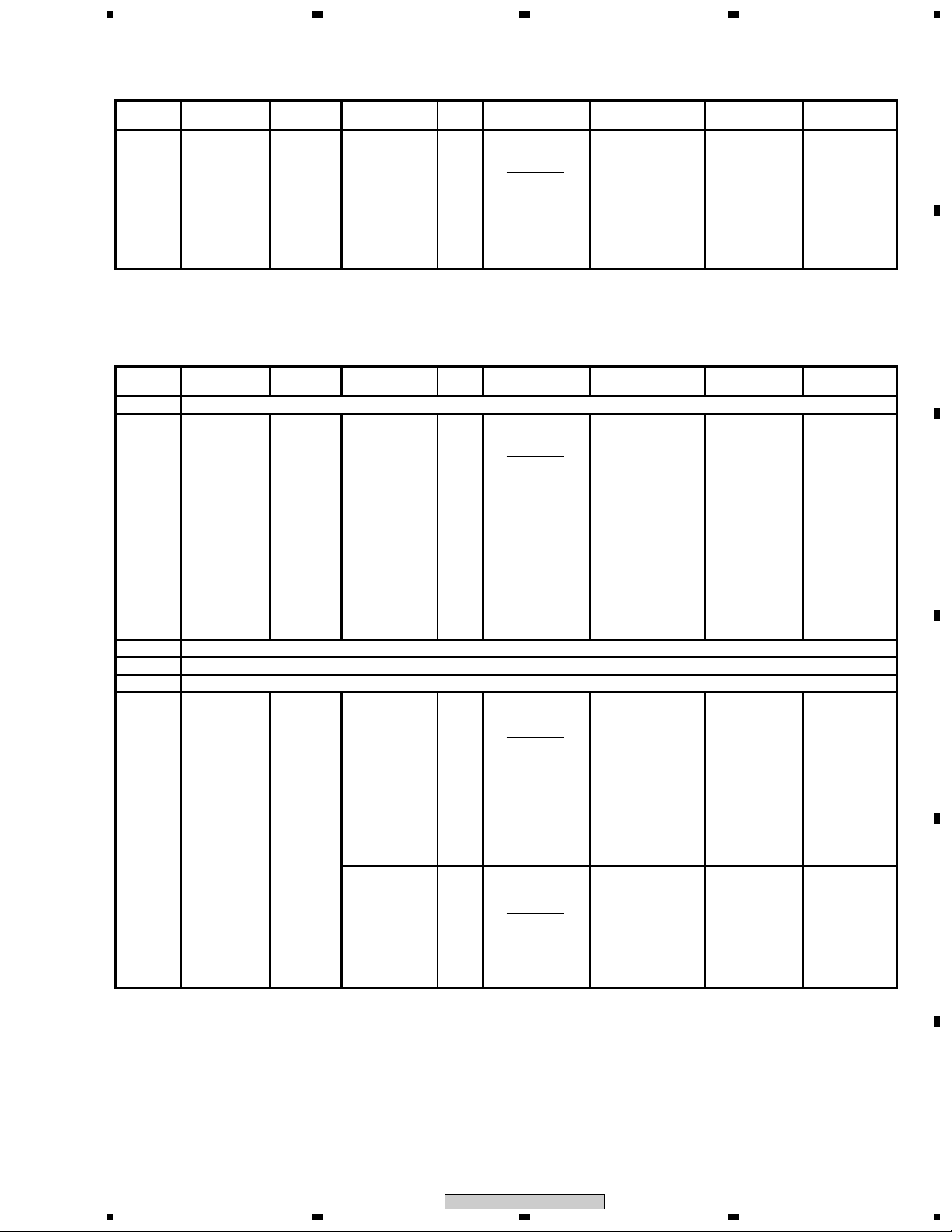
• I/O Assy Connection Specification
CN num
T1
T2 KM200NA13 1 SLOT_L 1 KM200NA13L SLOT I/F S1
(CN4001) (JST) 2 GND 2
T3
T4
T5
T6 KM200NA14 1 V+5.0V_STB 1 KM200NA10 MX AUDIO A1
(CN4006) (JST) 2 A_MUTE2 2
Part No.
Pin
Refer to the POWER SUPPLY Assy connection specification
3 SLOT_R 3
4 GND 4
5 +13.5V 5
6 GND 6
7 -9.0V 7
8 GND 8
9 +6.5V 9
10 +6.5V 10
11 GND 11
12 GND 12
13 +12V 13
Refer to the RGB Assy connection specification
Refer to the RGB Assy connection specification
Refer to the RGB Assy connection specification
3 GND 3
4 AUDIO_LOUT 4
5 GND 5
6 AUDIO_ROUT 6
7 GND 7
8 GND 8
9 +15V 9
10 +15V 10
11 +15V 1 B7B-PH-SM3 POWER SUPPLY P6
12 +15V 2
13 GND 3
14 GND 4
− NC 5
− NC 6
− NC 7
Pin Name
to Pin Continuation
Connection by
wire rod
ADX2784-
(J112)
Connection by
wire rod
ADX2786-
(J104)
Connection by
wire rod
ADX2786-
(J104)
Connection Former
Part No.
(JST) (CN8103)
(JST) (CN8601)
(JST)
Connection
Former Assy
Connection
Former CN num.
Connection
Former CN num.
A
B
C
D
E
F
PDP-433CMX
1
2
3
4
17
Page 18
1
23
• SLOT I/F and VIDEO SLOT Assys Connection Specification
<SLOT I/F Assy connection specification>
A
B
C
D
E
F
CN num
S1
S2
S3 AKM1220-
(CN8101)
Part No.
Pin
Refer to the RGB I/O Assy connection specification
Refer to the RGB Assy connection specification
162
161
160
159
158
157
156
155
154
153
152
149
148
147
146
145
144
143
142
141
140
139
138
137
136
135
134
133
132
131
130
129
128
127
126
125
124
123
122
121
120
119
118
117
116
115
114
113
112
111
110
109
108
107
Pin Name
GND
RA_PLK0
RA_PLK1
RA_PLK2
RA_PLK3
RA_PLK4
RA_PLK5
RA_PLK6
RA_PLK7
GND
GND
GA_PLK0
GA_PLK1
GA_PLK2
GA_PLK3
GA_PLK4
GA_PLK5
GA_PLK6
GA_PLK7
GND
GND
BA_PLK0
BA_PLK1
BA_PLK2
BA_PLK3
BA_PLK4
BA_PLK5
BA_PLK6
BA_PLK7
GND
CLK_PLK
GND
DE_PLK
GND
SCDT3
GND
GND
GND
+6.5V
+6.5V
SRIN
FUT1
IN4DET
IN5DET
+13.5V
+13.5V
+5V_STB
GND
-9.0V
GND
+12V
GND
GND
GND
to Pin Continuation
162
161
160
159
158
157
156
155
154
153
152
149
148
147
146
145
144
143
142
141
140
139
138
137
136
135
134
133
132
131
130
129
128
127
126
125
124
123
122
121
120
119
118
117
116
115
114
113
112
111
110
109
108
107
Boad to Boad − VIDEO SLOT V1
Connection
Former Part No.
Connection
Former Assy
4
Connection
Former CN num.
(CN7401)
18
1234
PDP-433CMX
Page 19
5
678
CN num
Part No.
Pin
106
105
104
103
102
101
62
61
60
59
58
57 BB_PLK3 57
56
55
54
53
52
49
48
47
46
45
44
43
42
41
40
39
38
37
36
35
34
33
32
31
30
29
28
27
26
25
24
23
22
21
20
19
18
17
16
15
14
13
12
11
Pin Name
SDA
GND
SCL
GND
GND
GND
GND
BB_PLK7
BB_PLK6
BB_PLK5
BB_PLK4
BB_PLK2
BB_PLK1
BB_PLK0
GND
GND
GB_PLK7
GB_PLK6
GB_PLK5
GB_PLK4
GB_PLK3
GB_PLK2
GB_PLK1
GB_PLK0
GND
GND
RB_PLK7
RB_PLK6
RB_PLK5
RB_PLK4
RB_PLK3
RB_PLK2
RB_PLK1
RB_PLK0
GND
GND
HD_PLK
GND
VD_PLK
GND
HD_PLKU
GND
VD_PLKU
+6.5V
+6.5V
FUT2
FUT3
SDIN_SEL
SLOT_ST
GND
SLOT_R
GND
SLOT_L
GND
VD_PLD
to Pin Continuation
106
105
104
103
102
101
Connection
Former Part No.
62
61
60
59
58
56
55
54
53
52
49
48
47
46
45
44
43
42
41
40
39
38
37
36
35
34
33
32
31
30
29
28
27
26
25
24
23
22
21
20
19
18
17
16
15
14
13
12
11
Connection
Former Assy
Connection
Former CN num.
A
B
C
D
E
F
PDP-433CMX
5
6
7
8
19
Page 20
1
23
4
A
B
CN num
Part No.
Pin
10
Pin Name
GND
9
8
7
6
5
4
3
2
1
HD_PLD
GND
SIG3(CR)
GND
SIG2(CB)
GND
SIG1(Y)
GND
GND
to Pin Continuation
10
9
8
7
6
5
4
3
2
1
Connection
Former Part No.
Connection
Former Assy
Connection
Former CN num.
<VIDEO SLOT Assy connection specification>
CN num
V1
Part No.
Pin
Refer to the SLOT I/F Assy connection specification (above)
Pin Name
to Pin Continuation
Connection
Former Part No.
Connection
Former Assy
C
Connection
Former CN num.
• MX AUDIO, SP OUT L and SP OUT R Assys Connection Specifications
<MX AUDIO Assy connection specification>
CN num
A1
A3 B8B-PH-SM3-TBB 1 L_OUT 1 Connection by wire rod
(CN8604) (JST) 2 L_GND 2
D
A5
A6 B3B-ZR-3.4 1 FAN_D 1 FAN
(CN8704) (JST) 2 FAN_PD 2 ADX2780- −−
A7 B3B-ZR-3.4 1 FAN_D 1 FAN
(CN8701) (JST) 2 FAN_PD 2 −− −
Part No.
Pin
Pin Name
Refer to the RGB I/O Assy connection specification
3 +5.0V_STB 3
4 TEMPIII 4
5 GND 5
6 N.C 6
7 R_OUT 1 S3B-PH-SM3-TBB SP OUT R SPR1
8 R_GND 2(NC) ADX2787- (JST) (CN8177)
− 3 (J109)
Refer to the RGB Assy connection specification
3 GND 3 (J115)
3 GND 3
to Pin Continuation
ADX2787-
(J109)
Connection by wire rod
Connection by wire rod
Connection
Former Part No.
S6B-PH-SM3-TBB SP OUT L SPL1
(JST) (CN8152)
Connection
Former Assy
Connection
Former CN num.
<SP OUT L Assy connection specification>
E
CN num
SPL1
Part No.
Pin
Pin Name
Refer to the MX AUDIO Assy connection specification (above)
to Pin Continuation
Connection
Former Part No.
Connection
Former Assy
Connection
Former CN num.
<SP OUT R Assy connection specification>
CN num
SPR1
Part No.
Pin
Pin Name
Refer to the MX AUDIO Assy connection specification (above)
to Pin Continuation
Connection
Former Part No.
Connection
Former Assy
Connection
Former CN num.
F
20
PDP-433CMX
1234
Page 21
1
234
• SUB ADDRESS A&B, ADDRESS RESONANCE, ADDRESS CONNECT A - D and
BRIDGE A-D Assys Connection Specifications
<SUB ADDRESS A&B Assy connection specification>
CN num
SAA1,SAB1
SAA2,SAB2
SAA3 AK P-1121-A-TFB 1 ADR OUT 1 Boad to Boad AKP-1121-A-TFB ADR RES K1 (Upper side)
(CN8803) 2 NC 2 (Upper side) (CN6701)
SAB3
(CN8903) 4 ADR.GND 4 (Lower side) (CN6701)
SAA3,SAB3 8 NC 8
common use 9 VADR 9 upper and lower
Part No.
AKP-1121-A-TFB
Pin
Pin Name
Refer to the POWER SUPPLY Assy connection specification
Refer to the DIGITAL VIDEO Assy connection specification
3 N C 3 Boad to Boad AKP-1121-A-TFB ADR RES K1 (Lower side)
5 ADR.GND 5
6 ADR.GND 6
7NC7
10 VADR 1 0
11 VADR 1 1
12 NC 12
13 NC 13
14 GND_D 1 4
15 GND_D 1 5
16 GND_D 1 6
17 +12V 17
18 +12V 18
19 +12V 19
20 ADR_B 20
21 ADR_U 21
22 ADR_D 2 2
23 SW 23
to Pin Continuation
Connection
Former Part No.
Connection
Former Assy
Connection
Former CN num.
K1 pin assignment
is common
A
B
C
<ADDRESS RESONANCE Assy connection specification>
CN num
K1(upper and lower is common)
K2 (upper side)
(CN6702)
K3 (upper side)
K4 (upper side) PCBs touch it 1 ADR OUT 2 1 − ADR CON AB3 (upper side)
K5 (upper side) PCBs touch it 1 ADR OUT 2 1 − ADR CON AC2 (upper side)
K2 (lower side)
(CN6702)
K3 (lower side)
K4 (lower side) PCBs touch it 1 ADR OUT 2 1 PCB touches it
K5 (lower side) PCBs touch it 1 ADR OUT 2 1 PCB touches it − ADR CON AC2 (lower side)
Part No.
B4B-PH-SM3-TBB
(JST)
B4B-PH-SM3-TBB
(JST)
Pin
Pin Name
Refer to the SUB ADDRESS A&B Assy connection specification
1
2
3
4
Refer to the POWER SUPPLY Assy connection specifications
1
2
3
4
Refer to the POWER SUPPLY Assy connection specifications
VADR
VADR
VADR
VADR
VADR
VADR
VADR
VADR
to Pin Continuation
1
Connection by wire rod
ADX2783- (J116)
4
Connection by wire rod
1
4 ADX2783- (J116)
PCB touches it
PCB touches it
Connection by wire rod
1
4
ADX2783- (J117)
Connection by wire rod
1
4 ADX2783- (J117)
Connection
Former Part No.
B4B-PH-SM3-TBB
(JST)
B4B-PH-SM3-TBB
(JST)
B4B-PH-SM3-TBB
(JST)
B4B-PH-SM3-TBB
(JST)
− ADR CON AB3 (lower side)
Connection
Former Assy
BRIDGE B BGB1
BRIDGE A BGA1
BRIDGE C BGC1
BRIDGE D BGD1
Connection
Former CN num.
(CN6431)
(CN6421)
(CN6441)
(CN6451)
D
E
F
PDP-433CMX
1
2
3
4
21
Page 22
1
23
4
A
B
C
<ADDRESS CONNECT A - D Assys connection specification>
CN num
AA1 (upper side)
AB1 (upper side)
AC1 (upper side)
AD1 (upper side)
AA2 (upper side) OPEN −− − − −
AA3 (upper side) PCBs touch it 1 ADR OUT 1 1 PCB touches it − BRIDGE A
AB2 (upper side) PCBs touch it 1 ADR OUT 1 1 PCB touches it − BRIDGE A
AB3 (upper side)
AC2 (upper side)
AC3 (upper side) PCBs touch it 1 ADR OUT 1 1 PCB touches it − BRIDGE B
AD2 (upper side) PCBs touch it 1 ADR OUT 1 1 PCB touches it − BRIDGE B
AD3 (upper side) OPEN −− − − −
AA1 (under side)
AB1 (under side)
AC1 (under side)
AD1 (under side)
AA2 (under side) OPEN −− − − −
AA3 (under side) PCBs touch it 1 ADR OUT 2 1 PCB touches it
AB2 (under side) PCBs touch it 1 ADR OUT 2 1 −
AB3 (under side)
AC2 (under side)
AC3 (under side) PCBs touch it 1 ADR OUT 2 1 −
AD2 (under side) PCBs touch it 1 ADR OUT 2 1 − BRIDGE C
AD3 (under side) OPEN −− − − −
Part No.
Pin
Refer to the DIGITAL VIDEO Assy connection specification
Refer to the ADDRESS RESONANCE Assy connection specification (above)
Refer to the DIGITAL VIDEO Assy connection specification
Refer to the ADDRESS RESONANCE Assy connection specification (above)
Pin Name
to Pin Continuation
PCB touches it
PCB touches it
PCB touches it
Connection
Former Part No.
− BRIDGE D
Connection
Former Assy
−
−
−
BRIDGE D
BRIDGE C
−
<BRIDGE A - D Assys connection specification>
CN num
BGA1
BGA2
BGA3
BGB1
D
BGB2
BGB3
BGC1
BGC2
BGC3
BGD1
BGD2
BGD3
Part No.
Pin
Refer to the ADDRESS RESONANCE Assy connection specification (above)
Refer to the ADDRESS CONNECT A - D Assys connection specification (above)
Refer to the ADDRESS RESONANCE Assy connection specification (above)
Refer to the ADDRESS CONNECT A - D Assys connection specification (above)
Refer to the ADDRESS RESONANCE Assy connection specification (above)
Refer to the ADDRESS CONNECT A - D Assys connection specification (above)
Refer to the ADDRESS RESONANCE Assy connection specification (above)
Refer to the ADDRESS CONNECT A - D Assys connection specification (above)
Pin Name
to Pin Continuation
Connection
Former Part No.
E
Connection
Former Assy
F
22
PDP-433CMX
1234
Page 23
1
234
• Y DRIVE, SCAN A&B, X DRIVE, X CONNECT A and B Assys Connection
Specifications
<Y DRIVE Assy connection specification>
CN num
Y1
Y2
Y3 AKM1200- 1 VH 1 BRIDGE CN AKP1218- -TFB SCAN A SA1
(CN2502) 2 VH 2 (CN6201)
Y4 −
Y5 AKM1200- 1 VH 1 BRIDGE CN AKP1218- -TFB SCAN B SB1
(CN2501) 2 VH 2 (CN6001)
Y6 − 1 PSUS 1 SCAN B SB2
Part No.
Pin
Refer to the POWER SUPPLY Assy connection specification
Refer to the DIGITAL VIDEO Assy connection specification
10 OC1 10
11 (AB) 11
12 SI 2 12
13 SI 1 13
14 GND.H 14
15 IC5.0V 15
10 OC1 10
11 A/B 11
12 SI 1 12
13 SI 2 13
14 GND.H 14
15 IC5.0V 15
Pin Name
3NC3
4NC4
5 OC2-2 5
6 OC2-1 6
7LE7
8 CLK 8
9 CLR 9
1 PSUS 1
3NC3
4NC4
5 OC2-1 5
6 OC2-2 6
7LE7
8 CLK 8
9 CLR 9
to Pin Continuation
Hot metal
connection
Hot metal
connection
Connection
Former Part No.
Tighten screw at
SCAN A
Tighten screw at
SCAN B
Connection
Former Assy
SCAN A SA2
Connection
Former CN num.
A
B
C
D
E
F
PDP-433CMX
1
2
3
4
23
Page 24
1
23
4
A
<SCAN A and B Assys connection specification>
CN num
SA1
SA2
SB1
SB2
Part No.
Pin
Refer to the Y DRIVE Assy connection specification (above)
Pin Name
to Pin Continuation
Connection
Former Part No.
Connection
Former Assy
Connection
Former CN num.
<X DRIVE Assy connection specification>
CN num
B
X1
X2
X3 − 1 X PSUS 1 X CON A EA1
X4 − 1 X PSUS 1 X CON B EB1
Part No.
Pin
Refer to the POWER SUPPLY Assy connection specification
Refer to the DIGITAL VIDEO Assy connection specification
Pin Name
to Pin Continuation
Hot metal
connection
Hot metal
connection
Connection
Former Part No.
Tighten screw at
SCAN A
Tighten screw at
SCAN B
Connection
Former Assy
Connection
Former CN num.
<X CONNECTOR Assy connection specification>
CN num
EA1
C
EB1
Part No.
Pin
Refer to the X DRIVE Assy connection specification (above)
Pin Name
to Pin Continuation
Connection
Former Part No.
Connection
Former Assy
Connection
Former CN num.
D
E
F
24
1234
PDP-433CMX
Page 25
1
234
• CONTROL, KEY CONNECTOR, SIDE KEY, IR, MX LED and
THERMAL SENSOR Assys Connection Specifications
<CONTROL Assy connection specification>
CN num
C1
C3 B6B-PH-SM3-TBB 1 V+5.0V_STB 1 Connection by
(CN8007) (JST) 2 KEY1 2
Part No.
Pin
Pin Name
Refer to the RGB Assy connection specification
3
GND_STB 4
4 V+5.0V_STB 1 KM200NA3 I R RE1
5 GND_STB 2
6 REM 3 (J113)
to Pin Continuation
wire rod
3 (NC)
ADX2778-
(J113)
Connection by
wire rod
ADX2778-
Connection
Former Part No.
B4B-PH-SM3-TBB KEY CON KL2
(JST) (CN8301)
(JST) (CN8551)
<KEY CONNECTOR Assy connection specification>
CN num
KL1 AKM-1207- -TBB 1 E1 1 FFC AKM1207- -TBB SIDE KEY SW1
(CN8302) (KYOCERA ELCO) 2 E2 2 ADD1195- (KYOCERA ELCO) (CN8251)
KL2
Part No.
Pin
Pin Name
3 E3 3 (J213)
4F44
5F55
6F66
7F77
8 N.C 8
Refer to the CONTROL Assy connection specification (above)
to Pin Continuation
Connection
Former Part No.
Connection
Former Assy
Connection
Former Assy
Connection
Former CN num.
Connection
Former CN num.
A
B
C
<SIDE KEY Assy connection specification>
CN num
SW1
Part No.
Pin
Pin Name
Refer to the KEY CONNECTOR Assy connection specification (above)
to Pin Continuation
<IR Assy connection specification>
CN num
RE1
Part No.
Pin
Pin Name
Refer to the CONTROL Assy connection specification (above)
to Pin Continuation
<MX LED Assy connection specification>
CN num
L1
Part No.
Pin
Pin Name
Refer to the RGB Assy connection specification
to Pin Continuation
<THERMAL SENSOR Assy connection specification>
CN num
TE1
Part No.
Pin
Pin Name
Refer to the DIGITAL VIDEO Assy connection specification
to Pin Continuation
Connection
Former Part No.
Connection
Former Part No.
Connection
Former Part No.
Connection
Former Part No.
Connection
Former Assy
Connection
Former Assy
Connection
Former Assy
Connection
Former Assy
Connection
Former CN num.
Connection
Former CN num.
Connection
Former CN num.
Connection
Former CN num.
D
E
F
PDP-433CMX
1
2
3
4
25
Page 26
1
23
4
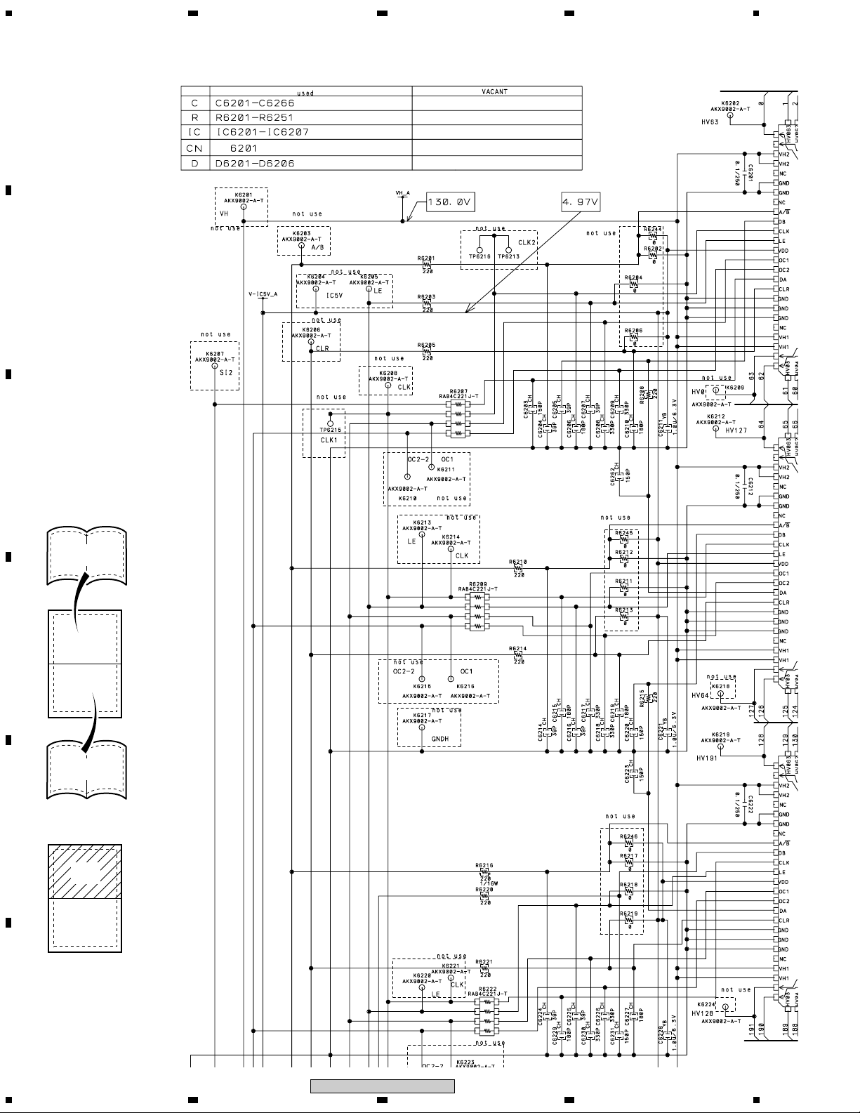
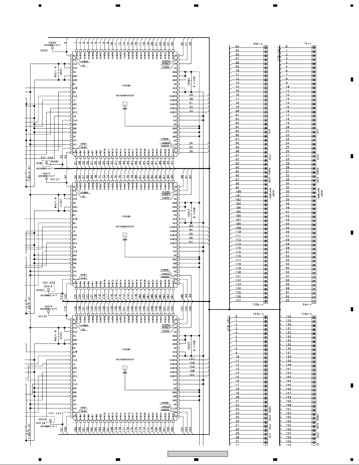
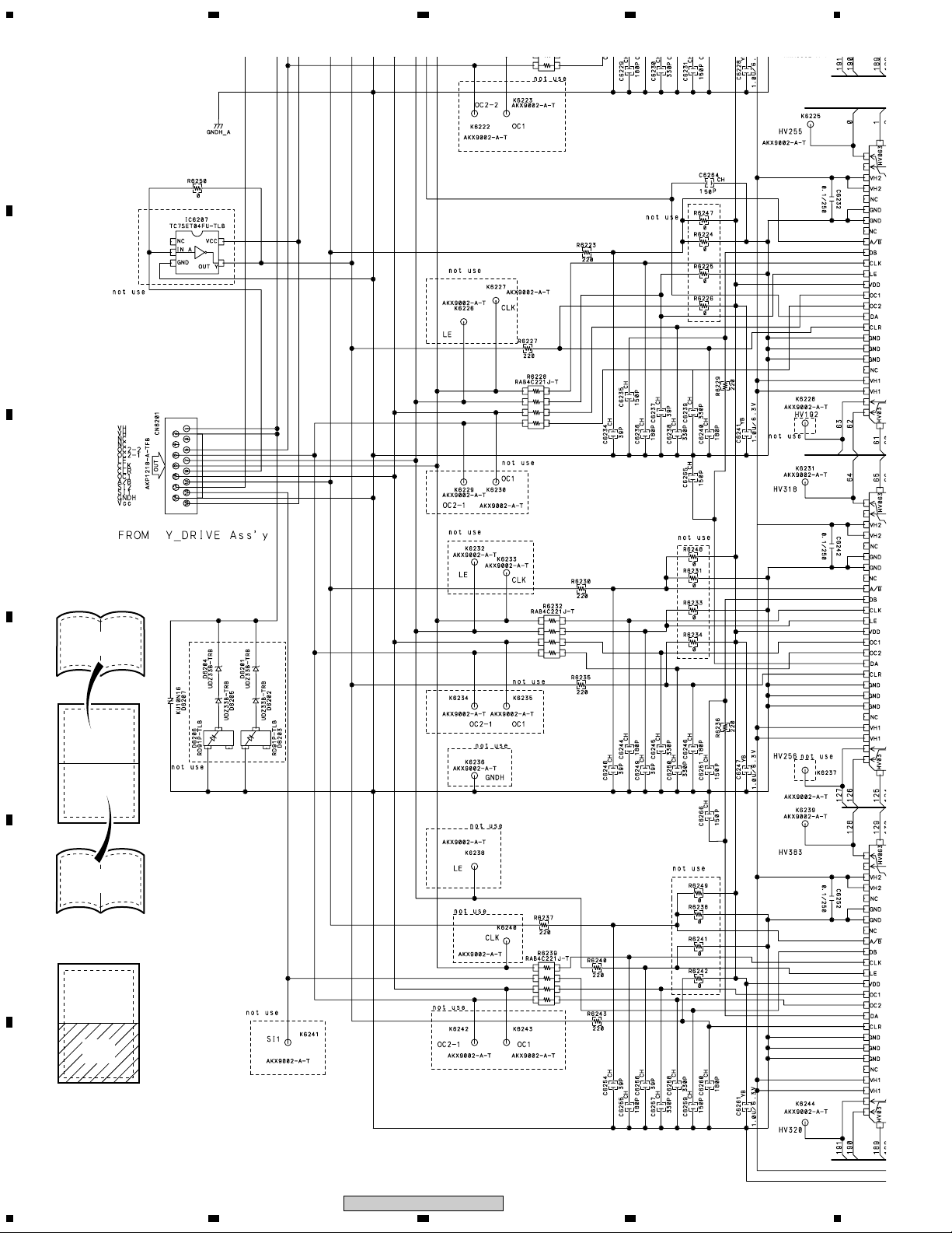
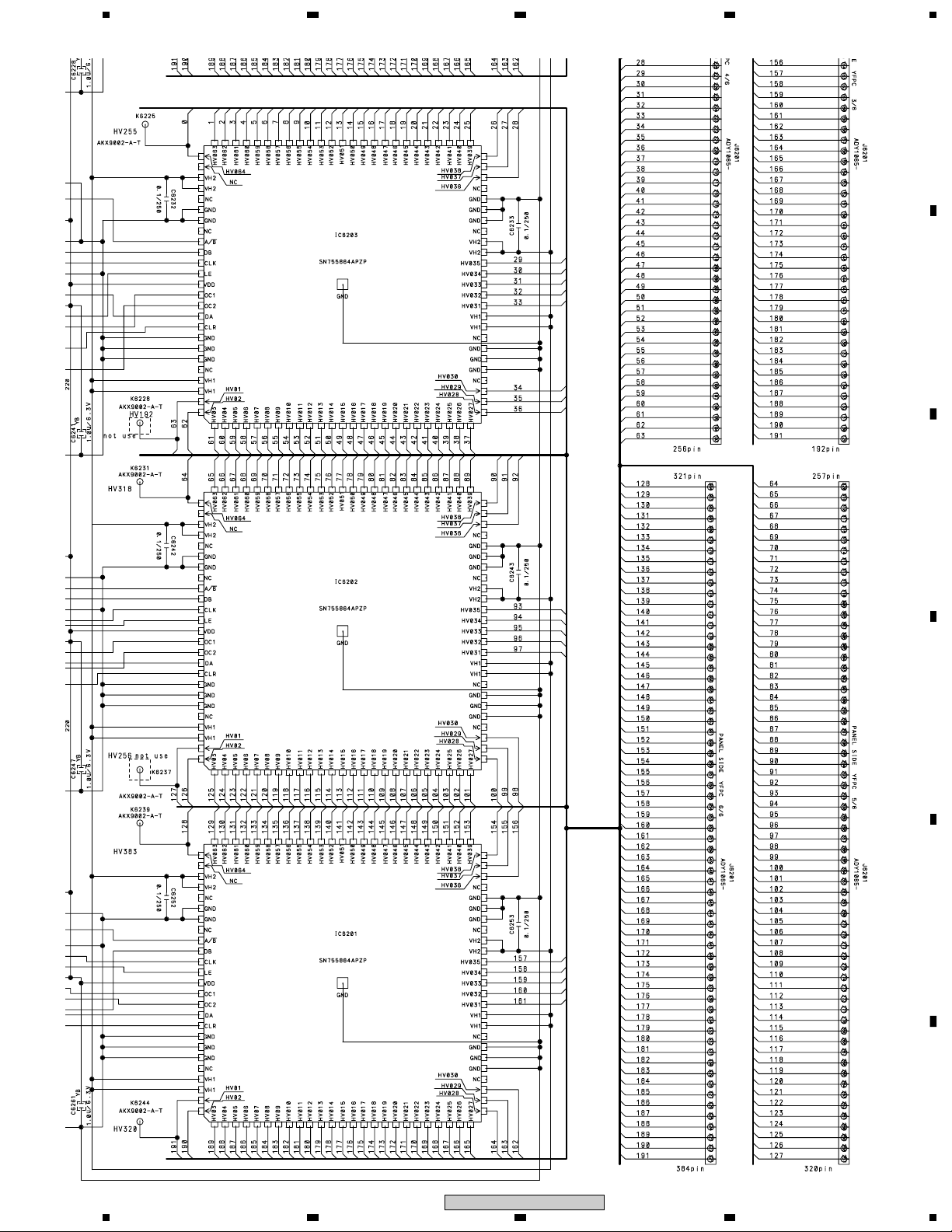
3.3 SCAN (A) ASSY
A
B
C
Large size
SCH diagram
D
E
1/2
2/2
1/2
F
26
1234
PDP-433CMX
Page 27
5
678
A
B
C
D
E
F
PDP-433CMX
5
6
7
8
27
Page 28
1
A
B
23
4
C
Large size
SCH diagram
1/2
D
2/2
E
2/2
F
28
1234
PDP-433CMX
Page 29
5
678
A
B
C
D
E
F
PDP-433CMX
5
6
7
8
29
Page 30
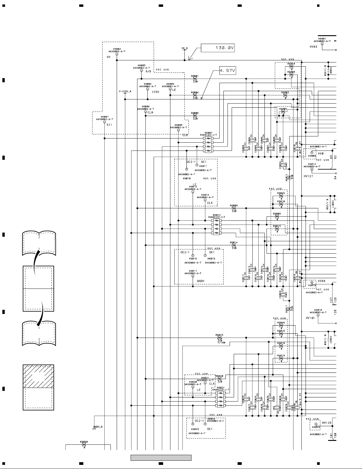
1
23
4
3.4 SCAN (B) ASSY
A
Vh
B
C
Large size
SCH diagram
1/2
D
2/2
E
1/2
F
30
1234
PDP-433CMX
Page 31

5
678
A
B
C
D
E
F
PDP-433CMX
5
6
7
8
31
Page 32

1
A
B
23
4
C
Large size
SCH diagram
1/2
D
2/2
E
2/2
F
32
1234
PDP-433CMX
Page 33

5
678
A
B
C
D
E
F
PDP-433CMX
5
6
7
8
33
Page 34

1
23
4
A
3.5 X CONNECTOR A and B ASSYS
B
C
D
E
F
34
1234
PDP-433CMX
Page 35

1
234
3.6 BRIDGE A - D ASSYS
• BRIDGE A-D
A
B
C
D
E
F
PDP-433CMX
1
2
3
4
35
Page 36

1
23
4
3.7 ADR CONNECT A ASSY
A
• ADR CONNECT A
B
C
D
E
F
AWV1928
36
1234
PDP-433CMX
Page 37

5
678
A
B
47/6.3
C
D
47/6.3
E
47/6.3
F
PDP-433CMX
5
6
7
8
37
Page 38

1
23
4
A
3.8 ADR CONNECT B ASSY
• ADR CONNECT B
B
C
D
E
F
AWV1928
38
1234
PDP-433CMX
Page 39

5
678
A
B
47/6.3
C
D
47/6.3
E
47/6.3
F
PDP-433CMX
5
6
7
8
39
Page 40

1
23
4
A
3.9 ADR CONNECT C ASSY
• ADR CONNECT C
B
C
D
E
F
AWV1971
40
1234
PDP-433CMX
Page 41

5
678
A
B
47/6.3
C
D
47/6.3
E
47/6.3
F
PDP-433CMX
5
6
7
8
41
Page 42

1
23
4
A
3.10 ADR CONNECT D ASSY
• ADR CONNECT D
B
C
D
E
F
AWV1971
42
1234
PDP-433CMX
Page 43

5
678
A
B
47/6.3
C
D
47/6.3
E
47/6.3
F
PDP-433CMX
5
6
7
8
43
Page 44

1
23
4
3.11 ADR RESONANCE ASSY
A
• ADR RESONANCE
B
C
D
E
F
44
1234
PDP-433CMX
Page 45

5
678
A
B
C
D
E
F
PDP-433CMX
5
6
7
8
45
Page 46

1
23
4
3.12 X DRIVE ASSY (1/3)
A
B
• X LOGIC BLOCK
C
D
E
F
46
1234
PDP-433CMX
Page 47

5
678
A
B
C
D
E
F
PDP-433CMX
5
6
7
8
47
Page 48

1
4
97V
3.13 X DRIVE ASSY (2/3)
23
4
A
• X SUS BLOCK
B
4.97V
.
C
14.95V
215 V
D
E
14.95 V
F
48
1234
PDP-433CMX
Page 49

5
678
4.97V
14.95V
215 V
1/2
2/2
Large size
SCH diagram
1/2
A
B
C
14.81 V
D
14.3 V 5.2 V
E
14.39 V
F
PDP-433CMX
5
6
7
8
49
Page 50

1
A
B
23
4
299
C
Large size
SCH diagram
1/2
D
2/2
E
2/2
F
50
1234
PDP-433CMX
Page 51

5
678
A
B
C
D
E
F
PDP-433CMX
5
6
7
8
51
Page 52

1
23
4
A
3.14 X DRIVE ASSY (3/3)
• X D-D CON BLOCK
B
C
D
E
F
52
1234
PDP-433CMX
Page 53

5
678
A
B
C
D
E
F
PDP-433CMX
5
6
7
8
53
Page 54

1
23
4
3.15 Y DRIVE ASSY (1/4)
A
B
• Y LOGIC DRIVE BLOCK
C
D
E
F
54
1234
PDP-433CMX
Page 55

5
678
A
B
C
D
E
F
PDP-433CMX
5
6
7
8
55
Page 56

1
23
4
3.16 Y DRIVE ASSY (2/4)
A
• Y DRIVE SUS BLOCK
B
15. 7V
Vsus 215V
C
D
Vsus 215V
E
15.0V
5.03V
F
56
D1FL40-TRB G10
PDP-433CMX
K2219
1234
Page 57

5
678
A
215V
B
12.7V
C
Vofs 48.1V
D
E
F
PDP-433CMX
5
6
7
8
57
Page 58

1
23
4
3.17 Y DRIVE ASSY (3/4)
A
B
• Y DRIVE SCAN BLOCK
C
D
E
F
58
1234
PDP-433CMX
Page 59

5
678
A
B
C
D
E
F
PDP-433CMX
5
6
7
8
59
Page 60

1
23
4
3.18 Y DRIVE ASSY (4/4)
A
• Y DRIVE D-D CON BLOCK
B
C
D
E
F
60
1234
PDP-433CMX
Page 61

5
678
A
B
C
D
E
F
PDP-433CMX
5
6
7
8
61
Page 62

1
23
4
A
3.19 SUB ADDRESS A ASSY
• SUB ADDRESS A
B
C
D
E
F
62
1234
PDP-433CMX
Page 63

5
678
A
B
C
D
E
F
PDP-433CMX
5
6
7
8
63
Page 64

1
23
4
3.20 SUB ADDRESS B ASSY
A
B
• SUB ADDRESS B
C
D
E
F
64
1234
PDP-433CMX
Page 65

5
678
A
B
C
D
E
F
PDP-433CMX
5
6
7
8
65
Page 66

1
23
4
3.21 SLOT CONNECTOR ASSY
A
• SLOT CONNECTOR
B
C
D
E
F
66
1234
PDP-433CMX
Page 67

5
678
A
B
C
D
E
F
PDP-433CMX
5
6
7
8
67
Page 68

1
23
3.22 DIGITAL VIDEO ASSY (1/10)
4
A
B
C
• DIGITAL BLOCK
D
E
F
68
1234
PDP-433CMX
Page 69

5
678
A
B
C
D
E
F
PDP-433CMX
5
6
7
8
69
Page 70

1
23
4
3.23 DIGITAL VIDEO ASSY (2/10)
A
B
• PANEL UCOM BLOCK
C
D
E
F
70
1234
PDP-433CMX
Page 71

1
23
3.24 DIGITAL VIDEO ASSY (3/10)
4
A
• MODULE UCOM
BLOCK
B
C
D
E
F
72
1234
PDP-433CMX
Page 72

5
678
A
B
C
D
E
F
PDP-433CMX
5
6
7
8
73
Page 73

1
23
3.25 DIGITAL VIDEO ASSY (4/10)
4
A
• IC31 L BLOCK
Large size
SCH diagram
1/2
B
2/2
C
1/2
D
E
F
74
1234
PDP-433CMX
Page 74

5
678
A
B
C
D
E
F
PDP-433CMX
5
6
7
8
75
Page 75

1
A
B
23
4
C
Large size
SCH diagram
1/2
D
2/2
E
2/2
F
76
1234
PDP-433CMX
Page 76

5
678
A
B
C
D
E
F
PDP-433CMX
5
6
7
8
77
Page 77

1
23
3.26 DIGITAL VIDEO ASSY (5/10)
4
A
• IC31 R BLOCK
Large size
SCH diagram
1/2
B
2/2
C
1/2
D
E
F
78
1234
PDP-433CMX
Page 78

5
678
A
B
C
D
E
F
PDP-433CMX
5
6
7
8
79
Page 79

1
A
B
23
4
C
Large size
SCH diagram
1/2
D
2/2
E
2/2
F
80
1234
PDP-433CMX
Page 80

5
678
A
B
C
D
E
F
PDP-433CMX
5
6
7
8
81
Page 81

1
23
4
3.27 DIGITAL VIDEO ASSY (6/10)
A
B
C
D
E
F
82
1234
PDP-433CMX
Page 82

5
678
• ADDRESS
CONNECTOR
U BLOCK
A
B
C
D
E
F
PDP-433CMX
5
6
7
8
83
Page 83

1
23
4
3.28 DIGITAL VIDEO ASSY (7/10)
A
• ADDRESS
CONNECTOR
D BLOCK
B
C
D
E
F
84
1234
PDP-433CMX
Page 84

5
678
A
B
C
D
E
F
PDP-433CMX
5
6
7
8
85
Page 85

1
23
4
3.29 DIGITAL VIDEO ASSY (8/10)
A
• IC23 BLOCK
B
C
D
E
F
86
1234
PDP-433CMX
Page 86

5
678
A
B
C
D
E
F
PDP-433CMX
5
6
7
8
87
Page 87

1
23
4
A
3.30 DIGITAL VIDEO ASSY (9/10)
• CLK GENERATOR BLOCK
B
C
D
E
F
88
1234
PDP-433CMX
Page 88

5
678
A
B
C
D
E
F
PDP-433CMX
5
6
7
8
89
Page 89

1
23
4
3.31 DIGITAL VIDEO ASSY (10/10)
A
• D-D CONV BLOCK
B
C
D
E
F
90
1234
PDP-433CMX
Page 90

5
678
A
B
C
D
E
F
PDP-433CMX
5
6
7
8
91
Page 91

1
23
4
3.32 I/O ASSY (1/2)
A
B
• REG BLOCK
C
D
E
F
92
1234
PDP-433CMX
Page 92

5
678
A
B
C
D
E
F
PDP-433CMX
5
6
7
8
93
Page 93

1
3.33 I/O ASSY (2/2)
23
4
A
B
C
• I/O BLOCK
D
E
F
94
1234
PDP-433CMX
Page 94

5
678
A
B
C
D
E
F
PDP-433CMX
5
6
7
8
95
Page 95

1
23
4
3.34 RGB ASSY (1/10)
A
B
• MATRIX BLOCK
C
D
E
F
96
1234
PDP-433CMX
Page 96

5
678
A
B
C
D
E
F
PDP-433CMX
5
6
7
8
97
Page 97

1
3.35 RGB ASSY (2/10)
23
4
A
• AD/PLL/AMP BLOCK
B
Large size
SCH diagram
1/2
C
2/2
D
E
1/2
F
98
1234
PDP-433CMX
Page 98

5
678
A
B
C
D
E
F
PDP-433CMX
5
6
7
8
99
Page 99

1
A
B
23
4
Large size
SCH diagram
1/2
C
D
2/2
2/2
E
F
100
1234
PDP-433CMX
Page 100

5
678
A
B
C
D
E
F
PDP-433CMX
5
6
7
101
8
 Loading...