

Page 1
PDP-433CMX
PLASMA DISPLAY
PDP-433CMX
PDP-433MXE
THIS MANUAL IS APPLICABLE TO THE FOLLOWING MODEL(S) AND TYPE(S).
Type
LUCBW ? − AC100 - 120V
YVLDK − ? AC100 - 240V
PDP-433CMX PDP-433MXE
This Service Manual should be used together with the following manual(s).
Model No. Order No. Remarks
Model
Power Requirement Remarks
ORDER NO.
ARP3155
PDP-433CMX
PDP-433MXE
The main parts having their serial numbers described in the table below are applicable to this service
manual. For details on replacing with the following parts, refer to Service Information for each part.
Model No.
PDP-433CMX/LUCBW 002201 – 005131 – 004721 – 005011 – 006121 – 006811 –
PDP-433MXE/YVLDK 002201 – 005131 – 004721 – 005011 – 006121 – 006811 –
For details, refer to "Important symbols for good services".
PIONEER CORPORATION 4-1, Meguro 1-chome, Meguro-ku, Tokyo 153-8654, Japan
PIONEER ELECTRONICS (USA) INC. P.O. Box 1760, Long Beach, CA 90801-1760, U.S.A.
PIONEER EUROPE NV Haven 1087, Keetberglaan 1, 9120 Melsele, Belgium
PIONEER ELECTRONICS ASIACENTRE PTE. LTD. 253 Alexandra Road, #04-01, Singapore 159936
c
PIONEER CORPORATION 2003
ARP3156 SCHEMATIC DIAGRAM and PCB DIAGRAM
Part numbers and serial numbers of the main parts applicable to this service manual
SW POWER
SUPPLY
MODULE
(AXY1059)
Rear Case
(ANE1608)
RGB ASSY
(AWZ6744)
DIGITAL VIDEO
ASSY
(AWV1971)
X DRIVE ASSY
(AWV1985)
T – ZZR MAR. 2003 Printed in Japan
Y DRIVE ASSY
(AWZ6748)
Page 2

SAFETY INFORMATION
This service manual is intended for qualified service technicians ; it is not meant for the casual do-ityourselfer. Qualified technicians have the necessary test equipment and tools, and have been trained
to properly and safely repair complex products such as those covered by this manual.
Improperly performed repairs can adversely affect the safety and reliability of the product and may
void the warranty. If you are not qualified to perform the repair of this product properly and safely, you
should not risk trying to do so and refer the repair to a qualified service technician.
WARNING
This product contains lead in solder and certain electrical parts contain chemicals which are known to the state of California to cause
cancer, birth defects or other reproductive harm.
NOTICE
(FOR CANADIAN MODEL ONLY)
Fuse symbols (fast operating fuse) and/or (slow operating fuse) on PCB indicate that replacement parts must
be of identical designation.
REMARQUE
(POUR MODÈLE CANADIEN SEULEMENT)
Les symboles de fusible (fusible de type rapide) et/ou (fusible de type lent) sur CCI indiquent que les pièces
de remplacement doivent avoir la même désignation.
Health & Safety Code Section 25249.6 – Proposition 65
SAFETY PRECAUTIONS
NOTICE :Comply with all cautions and safety related notes located
on or inside the cabinet and on the chassis.
The following precautions should be observed :
1. When service is required, even though the PDP UNIT an isolation
transformer should be inserted between the power line and the
set in safety before any service is performed.
2. When replacing a chassis in the set, all the protective devices
must be put back in place, such as barriers, nonmetallic knobs,
adjustment and compartment covershields, isolation resistorcapacitor, etc.
3. When service is required, observe the original lead dress. Extra
precaution should be taken to assure correct lead dress in the
high voltage circuitry area.
4. Always use the manufacture's replacement components.
Especially critical components as indicated on the circuit diagram
should not be replaced by other manufacture's.
Furthermore where a short circuit has occurred, replace those
components that indicate evidence of overheating.
5. Before returning a serviced set to the customer, the service
technician must thoroughly test the unit to be certain that it is
completely safe to operate without danger of electrical shock,
and be sure that no protective device built into the set by the
manufacture has become defective, or inadvertently defeated
during servicing. Therefore, the following checks should be
performed for the continued protection of the customer and
service technician.
6. Perform the following precautions against unwanted radiation
and rise in internal temperature.
• Always return the internal wiring to the original styling.
• Attach parts (Gascket, Ferrite Core, Ground, Rear Cover,
Shield Case etc.) surely after disassembly.
7. Perform the following precautions for the PDP panel.
• When the front case is removed, make sure nothing hits the
panel face, panel corner, and panel edge (so that the glass does
not break).
• Make sure that the panel vent does not break. (Check that the
cover is attached.)
• Handle the FPC connected to the panel carefully.
Twisting or pulling the FPC when connecting it to the connector
will cause it to peel off from the panel.
8. Pay attention to the following.
• Be sure to wire the fan. If the fan does not work, the temperature
will rise and cause the protection circuit to operate.
• When the front case is removed, infrared ray is radiated and
may disturb reception of the remote control unit.
• Pay extreme caution when the front case and rear panel are
removed because this may cause a high risk of disturbance to
TVs and radios in the surrounding.
2
PDP-433CMX
Page 3
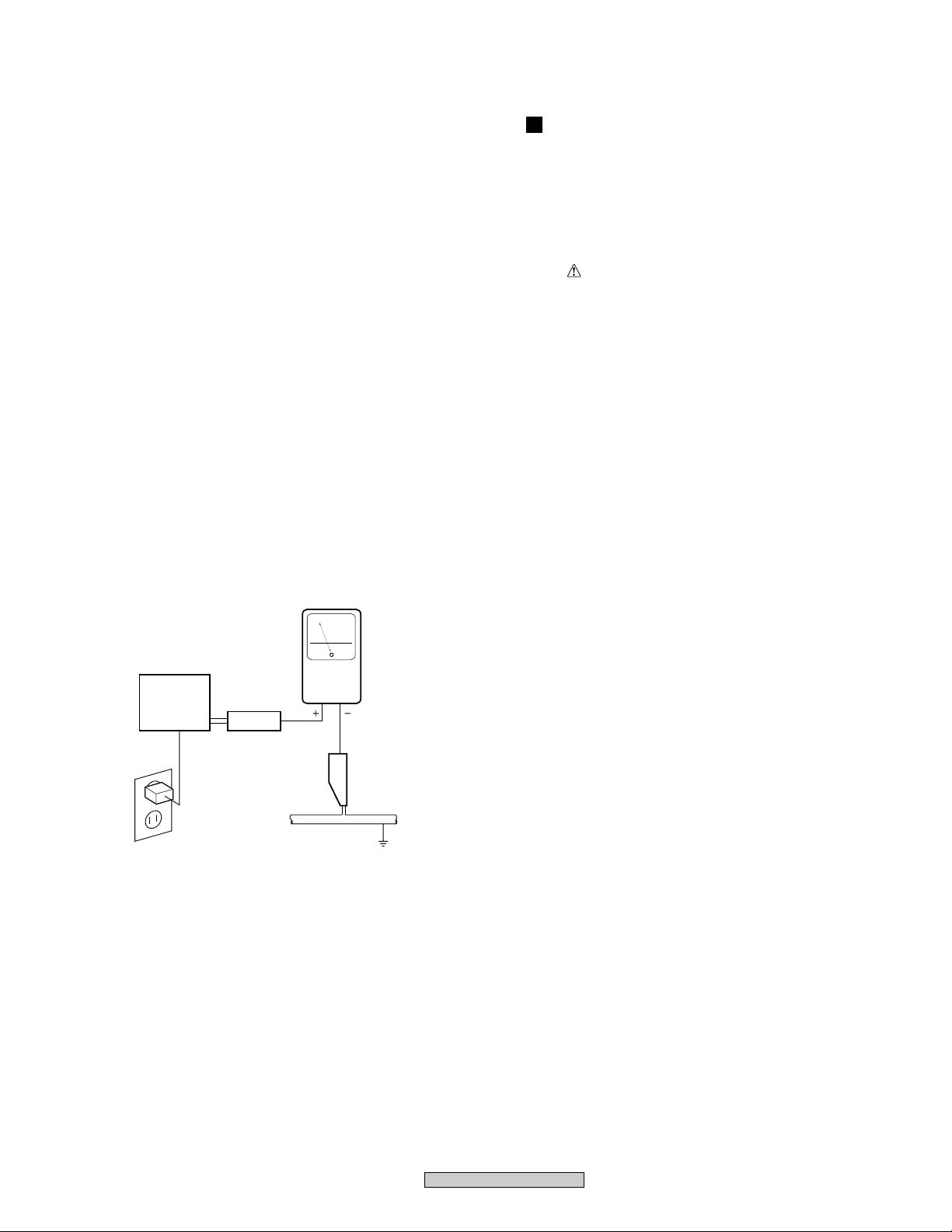
Leakage Current Cold Check
With the AC plug removed from an AC power source, place a
jumper across the two plug prongs. Turn the AC power switch on.
Using an insulation tester (DC 500V), connect one lead to the
jumpered AC plug and touch the other lead to each exposed metal
part (input/output terminals, screwheads, metal overlays, control
shafts, etc.), particularly any exposed metal part having a return
path to the chassis. Exposed metal parts having a return path to the
chassis should have a minimum resistor reading of 0.3MΩ and a
maximum resistor reading of 5MΩ. Any resistor value below or
above this range indicates an abnormality which requires corrective
action. Exposed metal parts not having a return path to the chassis
will indicate an open circuit.
Leakage Current Hot Check
Plug the AC line cord directly into an AC power source (do not use
an isolation transformer for this check).
Turn the AC power switch on.
Using a "Leakage Current Tester (Simpson Model 229 equivalent)",
measure for current from all exposed metal parts of the cabinet
(input/output terminals, screwheads, metal overlays, control shaft,
etc.), particularly any exposed metal part having a return path to the
chassis, to a known earth ground (water pipe, conduit, etc.). Any
current measured must not exceed 0.5mA.
PRODUCT SAFETY NOTICE
Many electrical and mechanical parts in PIONEER set have special
safety related characteristics. These are often not evident from
visual inspection nor the protection afforded by them necessarily
can be obtained by using replacement components rated for higher
voltage, wattage, etc. Replacement parts which have these special
safety characteristics are identified in this Service Manual.
Electrical components having such features are identified by marking
with a
Manual.
The use of a substitute replacement component which dose not have
the same safety characteristics as the PIONEER recommended
replacement one, shown in the parts list in this Service Manual, may
create shock, fire or other hazards.
Product Safety is continuously under review and new instructions
are issued from time to time. For the latest information, always
consult the current PIONEER Service Manual. A subscription to, or
additional copies of, PIONEER Service Manual may be obtained at
a nominal charge from PIONEER.
on the schematics and on the parts list in this Service
Reading should
not be above
0.5 mA
Earth ground
Device
under
test
Also test with plug
reversed
(Using AC adapter
plug as required)
Test all exposed
metal surfaces
Leakage
current
tester
AC Leakage Test
ANY MEASUREMENTS NOT WITHIN THE LIMITS
OUTLINED ABOVE ARE INDICATIVE OF A POTENTIAL
SHOCK HAZARD AND MUST BE CORRECTED BEFORE
RETURNING THE SET TO THE CUSTOMER.
PDP-433CMX
3
Page 4
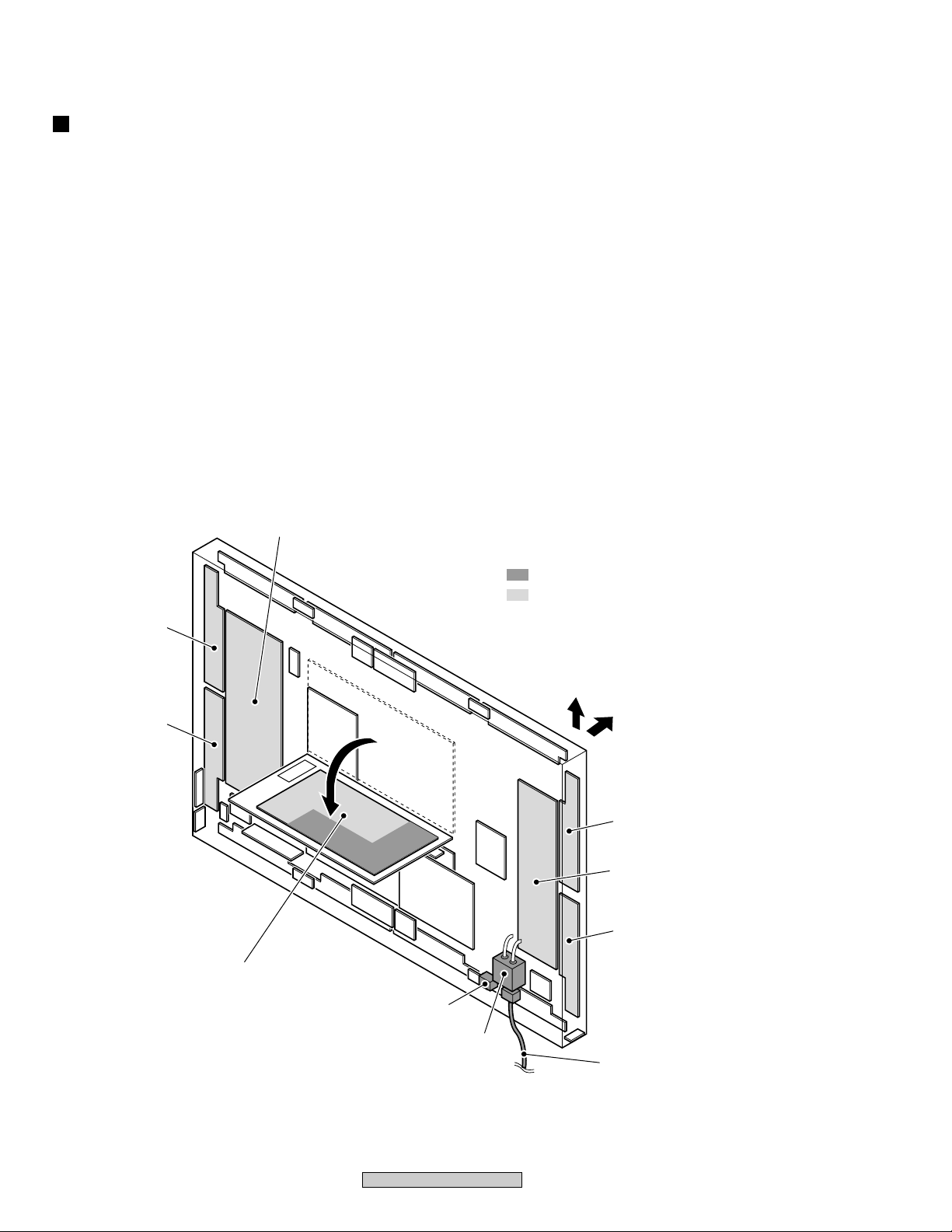
CHARGED SECTION AND HIGH VOLTAGE GENERATING POINT
7 Charged Section
The places where the commercial AC power is used without
passing through the power supply transformer.
If the places are touched, there is a risk of electric shock. In addition,
the measuring equipment can be damaged if it is connected to the
GND of the charged section and the GND of the non-charged
section while connecting the set directly to the commercial AC
power supply. Therefore, be sure to connect the set via an insulated
transformer and supply the current.
1. AC Power Cord
2. AC Inlet with Filter
3. Power Switch (S1)
4. Fuse (In the SW POWER SUPPLY Module)
5. STB Transformer and Converter Transformer
(In the SW POWER SUPPLY Module)
6. Other primary side of the SW POWER SUPPLY Module
Y DRIVE
Assy
SCAN (A)
Assy
7 High Voltage Generating Point
The places where voltage is 100V or more except for the charged
places described above. If the places are touched, there is a risk of
electric shock.
1. SW POWER SUPPLY Module ...................................... (215V)
2. X DRIVE Assy .............................................. (–280V to 215V)
3. Y DRIVE Assy ............................................................... (345V)
4. SCAN (A) Assy .............................................................. (345V)
5. SCAN (B) Assy ............................................................... (345V)
6. X CONNECTOR (A) Assy ........................... (–280V to 215V)
7. X CONNECTOR (B) Assy ............................ (–280V to 215V)
: Part is Charged Section.
: Part is the High Voltage Generating Points
other than the Charged Section.
SCAN (B)
Assy
Top
Front
X DRIVE
Assy
SW POWER SUPPLY
Module
Power Switch
(S1)
AC Inlet with Filter
Power Cord
Fig.1 Charged Section and High Voltage Generating Point (Rear View)
X CONNECTOR (A)
Assy
X CONNECTOR (B)
Assy
4
PDP-433CMX
Page 5
[ Important symbols for good services ]
In this manual, the symbols shown-below indicate that adjustments, settings or cleaning should be made securely.
When you find the procedures bearing any of the symbols, be sure to fulfill them:
1. Product safety
You should conform to the regulations governing the product (safety, radio and noise, and other regulations), and
should keep the safety during servicing by following the safety instructions described in this manual.
2. Adjustments
To keep the original performances of the product, optimum adjustments or specification confirmation is indispensable.
In accordance with the procedures or instructions described in this manual, adjustments should be performed.
3. Cleaning
For optical pickups, tape-deck heads, lenses and mirrors used in projection monitors, and other parts requiring cleaning,
proper cleaning should be performed to restore their performances.
4. Shipping mode and shipping screws
To protect the product from damages or failures that may be caused during transit, the shipping mode should be set or
the shipping screws should be installed before shipping out in accordance with this manual, if necessary.
5. Lubricants, glues, and replacement parts
Appropriately applying grease or glue can maintain the product performances. But improper lubrication or applying
glue may lead to failures or troubles in the product. By following the instructions in this manual, be sure to apply the
prescribed grease or glue to proper portions by the appropriate amount.For replacement parts or tools, the prescribed
ones should be used.
PDP-433CMX
5
Page 6

CONTENTS
SAFETY INFORMATION
1. SPECIFICATIONS
2. EXPLODED VIEWS AND PARTS LIST
2.1 PACKING .............................................................................................................................................. 8
2.2 UNDER LAYER SECTION(1) .................................................................................................................
2.3 UNDER LAYER SECTION(2)
2.4 UNDER LAYER SECTION(3)
2.5 UNDER LAYER SECTION(4)
2.6 UNDER LAYER SECTION(5) 16
2.7 UNDER LAYER SECTION(6)
2.8 MIDDLE LAYER SECTION(1)
2.9 MIDDLE LAYER SECTION(2) ............................................................................................................... 21
2.10 MIDDLE LAYER SECTION(3)
2.11 MIDDLE LAYER SECTION(4)
2.12 UPPER LAYER SECTION(1)
2.13 UPPER LAYER SECTION(2)
2.14 FRONT CASE SECTION
2.15 REAR SECTION
2.16 PDP SERVICE ASSY 433(AWU1069) ................................................................................................................. 30
2.17 PANEL CHASSIS(43) ASSY(AWU1067) ............................................................................................. 30
3. BLOCK DIAGRAM AND SCHEMATIC DIAGRAM ........................................................................................ 32
3.1 BLOCK DIAGRAM ................................................................................................................................... 32
3.1.1 OVERALL BLOCK DIAGAM
3.1.2 REG ASSY 34
3.1.3 DIGITAL VIDEO ASSY ....................................................................................................................... 36
3.1.4 X DRIVER ASSY ................................................................................................................................ 37
3.1.5 Y DRIVE ASSY .................................................................................................................................. 38
3.1.6 MX AUDIO ASSY ................................................................................................................................ 40
3.1.7 SUB ADDRESS A and B ASSYS .......................................................................................................
3.1.8 ADR RESONANCE ASSY
3.1.9 ADR CONNECT A, B, C and D ASSYS 42
3.1.10 VIDEO SIGNAL ROUTE .................................................................................................................. 43
3.1.11 SYNC SIGNAL ROUTE
3.2 WAVEFORMS
4. PCB CONNECTION DIAGRAM
5. PCB PARTS LIST .........................................................................................................................................
6. ADJUSTMENT............................................................................................................................................... 68
6.1 SERVICE FACTORY MODE ................................................................................................................... 68
6.1.1 State Transition Diagram
6.1.2 Table of Adjustment Items in Service Factory
6.1.3 Description of Service Factory Menu Display
6.2 ADJUSTMENT REQUIRED WHEN THE SET IS REPARED OR REPLACED
6.3 ADJUSTMENT
6.3.1 VIDEO CARD ADJUSTMENT
6.4 COMMANDS
6.4.1 RS-232C COMMANDS (for adjustment)
6.4.2 RS-232C COMMANDS (for setting)
7. GENERAL INFORMATION
7.1 DIAGNOSIS
7.1.1 CONFIGURATION OF THE PC BOARD
7.1.2 DIAGNOSIS FOR SHUTDOWN AND POWER-DOWN BY LED
7.1.3 AUTOMATIC BACKUP OF DIGITAL VIDEO ASSY DATA
7.1.4 DISASSEMBLY
7.2 IC INFORMATION
8. PANEL FACILITIES
..................................................................................................................................
........................................................................................................................................
.........................................................................................................
.................................................................................................................
.................................................................................................................
.................................................................................................................
.................................................................................................................
.................................................................................................................
.............................................................................................................
.............................................................................................................
.............................................................................................................
.............................................................................................................
...............................................................................................................
......................................................................................................................
...................................................................................................................................
...............................................................................................................
..........................................................................................................................................
..................................................................................................................
.............................................................................................
...................................................................................................................
......................................................................................................................................... 45
...........................................................................................(Refer to ARP3156)
...................................................................................................................
.....................................................................................
......................................................................................
........................................
.........................................................................................................................................
.............................................................................................................
............................................................................................................................................
.............................................................................................
...................................................................................................
...........................................................................................................................
.............................................................................................................................................
.............................................................................................
........................................................
..................................................................
...................................................................................................................................
...................................................................................................................................
........................................................................................................................................
2
7
8
10
11
12
14
18
20
22
23
24
26
28
29
32
41
42
44
54
68
71
73
103
104
104
112
112
113
125
125
125
126
136
138
142
173
6
PDP-433CMX
Page 7
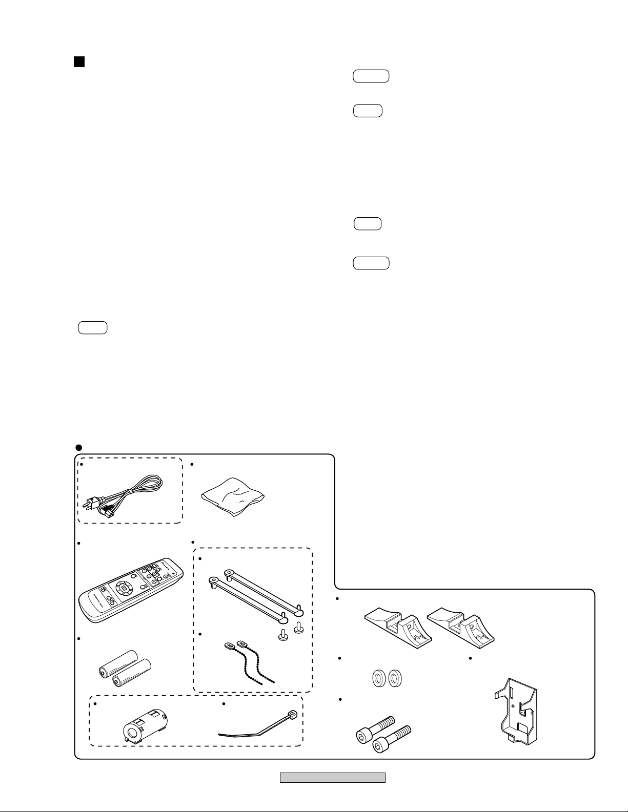
Accessories
Power Cord (ADG1208)
Remote Control Unit
(AXD1459)
Binder Assy (AEC1758)
PDP-433MXE only
PDP-433CMX only
Dry Cell Battery (R6P, AA)
Ferrite Core (ATX1031) Cable Tie
Display Stand (×2) (AMR3264)
Washer (×2) (WB80FZB)
Hex Hole Bolts (×2)
(SMZ80H400FZB)
Remote Control Unit Holder
(AMR3268)
Cleaning Cloth (for wiping front panel)
(AED1197)
Speed Clamp (×2)
Bead Bands (×2)
1. SPECIFICATIONS
General
Light emission panel ............ 43 inch plasma display panel
Number of pixels .............................................. 1024 x 768
Power supply .... AC 100 - 120 V, 50/60 Hz (PDP-433CMX)
Power supply .... AC 100 - 240 V, 50/60 Hz (PDP-433MXE)
Rated current .................... 2.98 A - 2.48 A (PDP-433CMX)
Rated current .................... 2.98 A - 1.24 A (PDP-433MXE)
Standby power consumption .......... 0.9 W (PDP-433CMX)
Standby power consumption .............. 1 W (PDP-433MXE)
External dimensions ........ 1070 (W) x 630 (H) x 98 (D) mm
............................. 42-1/8 (W) x 24-13/16 (H) x 3-7/8 (D) in.
(including display stand)
...................................... 1070 (W) x 653 (H) x 300 (D) mm
....................... 42-1/8 (W) x 25-23/32 (H) x 11-13/16 (D) in.
Weight............................................... 31.5 kg (69 lbs. 7 oz)
(including display stand) .................. 32.1 kg (70 lbs. 12 oz)
Input/output
Video
INPUT 1
Input Mini D-sub 15 pin (socket connector)
PLASMA DIAPLAY (PDP-433CMX and PDP-433MXE)
Output Mini D-sub 15 pin (socket connector)
INPUT 2
Input BNC jack (x5)
Audio
Input AUDIO INPUT (for INPUT 1/2)
Output AUDIO OUTPUT
Control
RGB signal (G ON SYNC compatible)
RGB ... 0.7 Vp-p/75 Ω/no sync.
HD/CS, VD ... TTL level
/positive and negative polarity
/2.2 kΩ
G ON SYNC
... 1 Vp-p/75 Ω/negative sync.
*Compatible with Microsoft’s Plug & Play
(VESA DDC1/2B)
RS-232C ... D-sub 9 pin (pin connector)
COMBINATION IN/OUT
CONTROL IN/OUT ... monaural mini jack (x2)
Accessories
Power cord ...................................... 1 (PDP-433CMX Only)
Remote control unit ......................................................... 1
Remote control unit holder .............................................. 1
AA (R6) batteries .............................................................. 2
Cleaning cloth ................................................................... 1
Speed clamps ................................................................... 2
Bead bands ...................................................................... 2
Warranty .......................................... 1 (PDP-433CMX Only)
Operating Instructions...................................................... 1
Display stands .................................................................. 2
Washers ........................................................................... 2
Hex hole bolts (M8X40).................................................... 2
Ferrite core ...................................... 1 (PDP-433MXE Only)
Cable tie .......................................... 1 (PDP-433MXE Only)
÷ Due to improvements, specifications and design are subject to
change without notice.
75 Ω/with buffer
RGB signal (G ON SYNC compatible)
RGB ... 0.7 Vp-p/75 Ω/no sync.
HD/CS, VD ... TTL level
/positive and negative polarity/
75 Ω or 2.2 kΩ
(impedance switch)
G ON SYNC ...
1 Vp-p/75 Ω/negative sync.
Stereo mini jack
L/R ... 500mVrms/more than 10 kΩ
Stereo mini jack
L/R ... 500mVrms (max)/less than 5 kΩ
SPEAKER
L/R ... 8 – 16 Ω/2W +2W (at 8 Ω)
... Mini DIN 6 pin (x2)
PDP-433CMX
7
Page 8
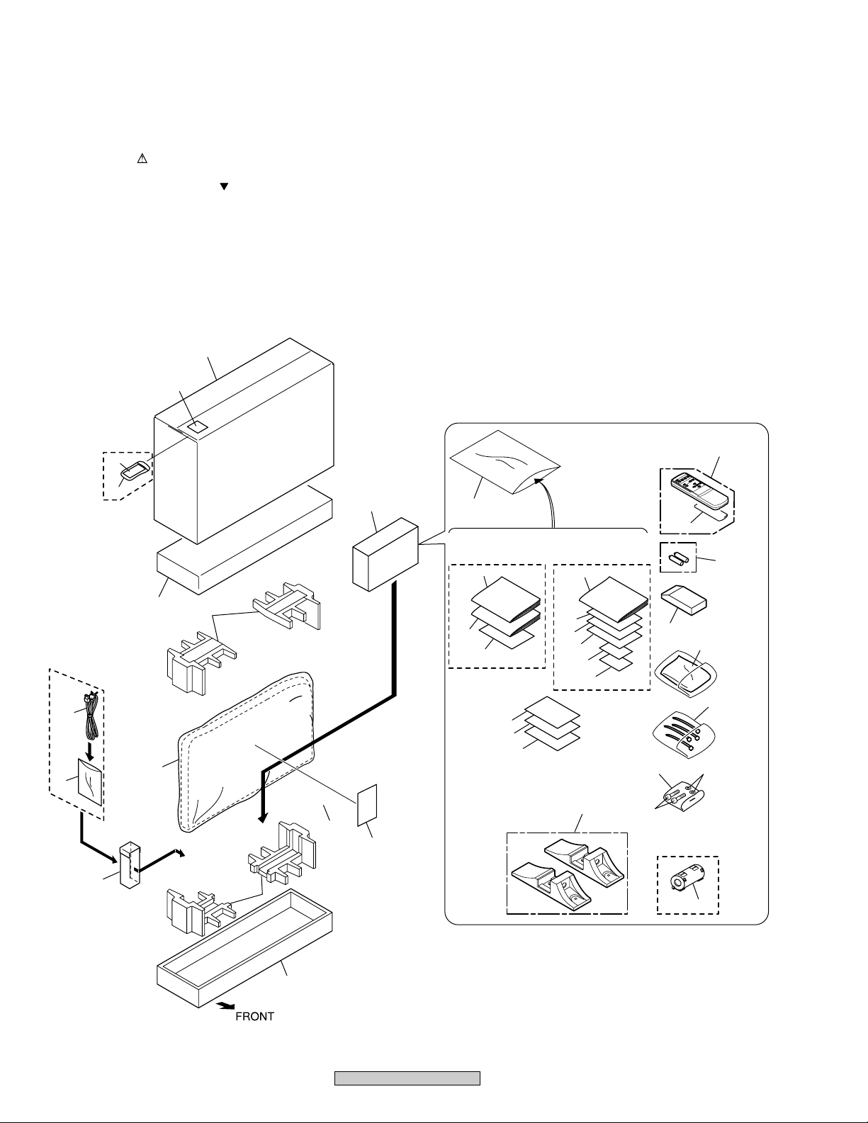
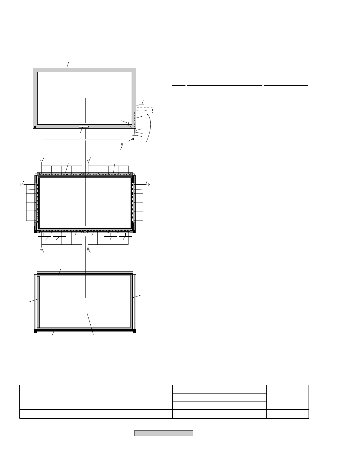
2. EXPLODED VIEWS AND PARTS LIST
NOTES:• Parts marked by "NSP" are generally unavailable because they are not in our Master Spare Parts List.
2.1 PACKING
The mark found on some component parts indicates the importance of the safety factor of the part.
•
Therefore, when replacing, be sure to use parts of identical designation.
Screws adjacent to mark on the product are used for disassembly.
•
For the applying amount of lubricants or glue, follow the instructions in this manual.
•
(In the case of no amount instructions, apply as you think it appropriate.)
1
37
PDP-433CMX
Only
18
10
7
27
PDP-433MXE
Only
34
PDP-433CMX
Only
33
20
21
22
PDP-433CMX
Only
23
27
6
2
5
3
35
32
14
15
16
8
16
4
2
12
11
13
17
28
19
29
26
30
PDP-433MXE
Only
25
24
31
36
8
PDP-433CMX
Page 9
(1) PACKING PARTS LIST
Mark No. Description Part No.
Mark No. Description Part No.
1 Packing Case See Contrast table (2)
2 Carton (43) AHD3100
3 Pad (43U) AHA2282
4 Pad (43L) AHA2283
5 Mirror Mat AHG1284
6 Power Cord Case AHC1037
7 Accessory Case Assy See Contrast table (2)
8 • • • • •
9 • • • • •
NSP 10 Polyethylene Bag See Contrast table (2)
11 Plasma Caution Sheet See Contrast table (2)
12 Plasma Caution Sheet See Contrast table (2)
13 Caution Sheet See Contrast table (2)
14 Caution Sheet ARM1194
15 Caution Sheet ARM1200
16 Caution Sheet ARM1201
17 Caution Sheet See Contrast table (2)
NSP 18 Warranty Card See Contrast table (2)
NSP 19 Warranty Card See Contrast table (2)
20 Remote Control Unit AXD1459
NSP 22 Dry Cell Battery (R6P, AA) AEX1026
21 Battery Cover AZN2462
23 Power Cord See Contrast table (2)
24 Binder Assy AEC1758
(Speed Clamp × 2, Bead Band × 2)
25 Wiping Cloth AED1208
NSP 26 Polyethylene Bag AHG-064
27 Vinyl Bag AHG1310
28 Display Stand AMR3264
29 Remote Control Holder AMR3268
30 Hex Hole Bolt SMZ80H400FZB
31 Washer WB80FZB
32 Plasma Caution Sheet See Contrast table (2)
33 Operating Instructions See Contrast table (2)
(Japanese/English/French)
34 Operating Instructions See Contrast table (2)
(Spanish/Italian/Dutch)
35 Operating Instructions See Contrast table (2)
(English/French/German)
36 Ferrite Core See Contrast table (2)
37 Warranty Card Contens Label See Contrast table (2)
(2) CONTRAST TABLE
PDP-433CMX/LUCB and PDP-433MXE/YVLDK are constructed the same except for the following :
Part No.
Mark No. Symbol and Description
1
Packing Case (43CMX)
1
Packing Case (43MXE)
7
Accessory Cord Case(43CMX)
7
NSP
NSP
NSP
Accessory Cord Case(43MXE)
10
Polyethylene Bag Assy
11
Plasma Caution Sheet
12
Plasma Caution Sheet
13
Caution Sheet
17
Caution Sheet
18
Warranty Card
19
Warranty Card
23
Power Cord
32
Plasma Caution Sheet
33
Operating Instructions (Japanese/English/French)
34
Operating Instructions (Spanish/Italian/Dutch)
35
Operating Instructions (English/French/German)
36
Ferrite Core
37
Warranty Card Contens Label
PDP-433CMX PDP-433MXE
LUCB YVLDK
AHD3130
Not used
AXX1058
Not used
AHG-195
ARM1145
ARM1147
ARM1176
ARM1203
ARY1093
ARY1102
ADG1208
Not used
ARD1052
Not used
Not used
Not used
AAX2911
Remarks
Not used
AHD3134
Not used
AXX1059
Not used
Not used
Not used
Not used
Not used
Not used
Not used
Not used
ARM1149
Not used
ARC1510
ARE1365
ATX1031
Not used
PDP-433CMX
9
Page 10
2.2 UNDER LAYER SECTION (1)
11 11
1
2 3 4
9
11
13
11
13
11
1010
5 or 6
12
Upper side
11
131313
10
11
9
7 or 8
10
1234
111111
10
PDP-433CMX
Page 11
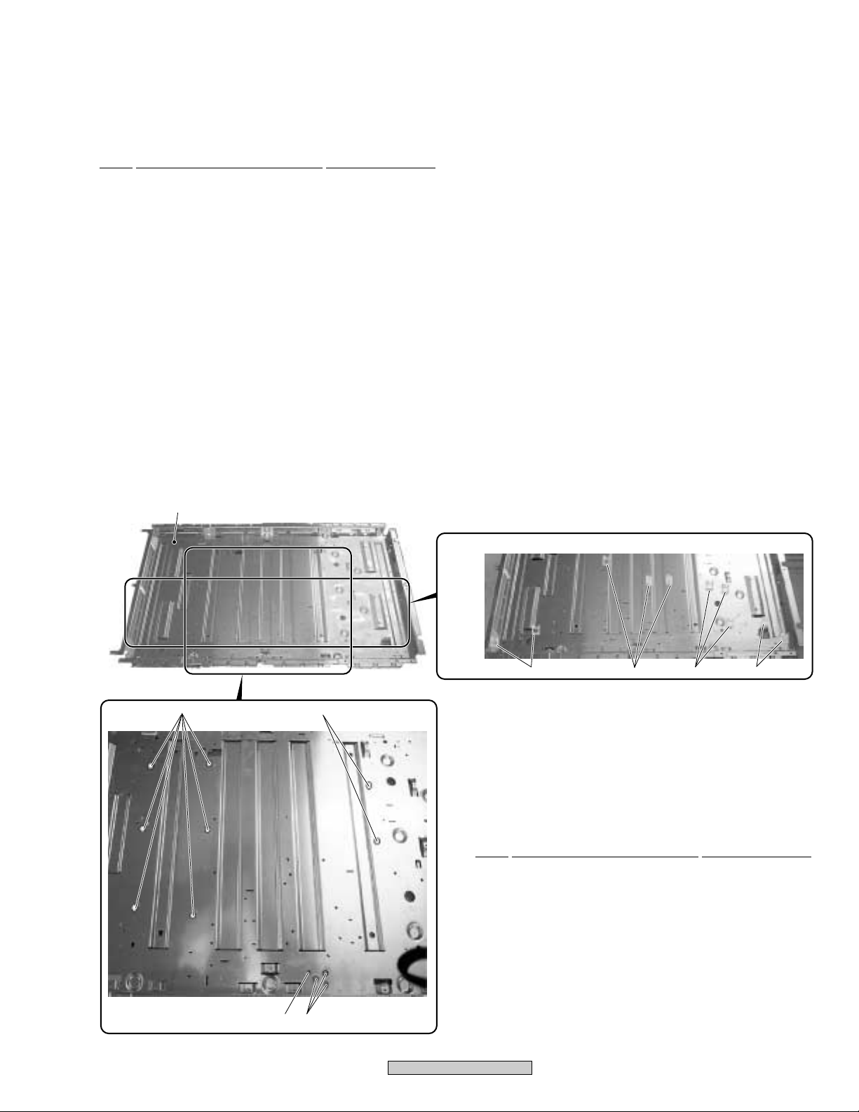
UNDER LAYER SECTION (1) PARTS LIST
•
Mark No. Description Part No.
NSP 1 ADR CONNECT A Assy AWZ6678
NSP 2 ADR CONNECT B Assy AWZ6679
NSP 3 ADR CONNECT C Assy AWZ6680
NSP 4 ADR CONNECT D Assy AWZ6681
NSP 5 BRIDGE A Assy AWZ6728
NSP 6 BRIDGE B Assy AWZ6729
NSP 7 BRIDGE C Assy AWZ6730
NSP 8 BRIDGE D Assy AWZ6731
NSP 9 ADR RESONANCE Assy AWZ6751
10 Screw ABA1301
11 Screw VBB30P100FNI
12 Shading Sheet (43) AMR3313
13 Rear Coner Label AAX2862
2.3 UNDER LAYER SECTION (2)
Refer to
"2.17 PANEL CHASSIS (43) ASSY
1
(AWU1067)".
5
2
2
UNDER LAYER SECTION (2) PARTS LIST
•
Mark No. Description Part No.
1 Panel Chassis (43) Assy AWU1067
[Refer to "2.17 PANEL CHASSIS (43) ASSY".]
2 Circuit Board Spacer AEC1872
NSP 4 PCB Spacer AEC1121
34
3 Circuit Board Spacer AEC1873
5 Wire Saddle AEC1904
PDP-433CMX
555
11
Page 12
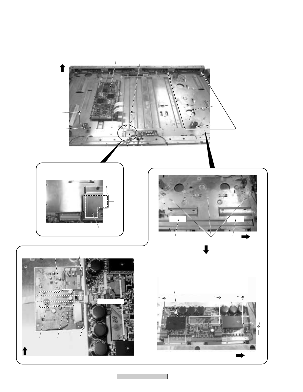
2.4 UNDER LAYER SECTION (3)
Upper side
13
4
1
5
13
13
4
5
Upper
side
314
9 8
14
6
X DRIVE Assy
14
11
12
2
14
11
14
Upper
side
15
Upper
side
12
PDP-433CMX
Page 13

UNDER LAYER SECTION (3) PARTS LIST
•
Mark No. Description Part No.
1 DIGITAL VIDEO Assy AWV1971
2 X DRIVE Assy AWV1985
NSP 4 Metal Fitting ANG2464
NSP 5 Heat Sink ANH1594
3 MX AUDIO Assy AWZ6644
6 Silicone Sheet AEH1039
7 • • • • •
8 Audio Sheet (43) AMR3285
9 Rivet BEC1066
10 • • • • •
11 Coil Silicone Sheet AEH1048
12 Circuit Board Spacer AEC1872
13 Screw ABZ30P060FMC
14 Screw VBB30P100FNI
15 Screw PMB30P060FNI
PDP-433CMX
13
Page 14
2.5 UNDER LAYER SECTION (4)
2
Upper
side
Upper side
Upper
side
10 10
8
9
8
8
1
9
14
5
7
6
PDP-433CMX
Page 15

UNDER LAYER SECTION (4) PARTS LIST
•
Mark No. Description Part No.
1 Y DRIVE Assy AWZ6748
2 Circuit Board Spacer AEC1872
3 • • • • •
4 • • • • •
5 Scan IC Spring (43L) ABK1029
6 Scan IC Spring (43R) ABK1030
7 Scan Insulation Sheet (43) AMR3287
8 Screw VBB30P100FNI
9 Screw PMB30P060FNI
10 Coil Silicone Sheet AEH1048
PDP-433CMX
15
Page 16
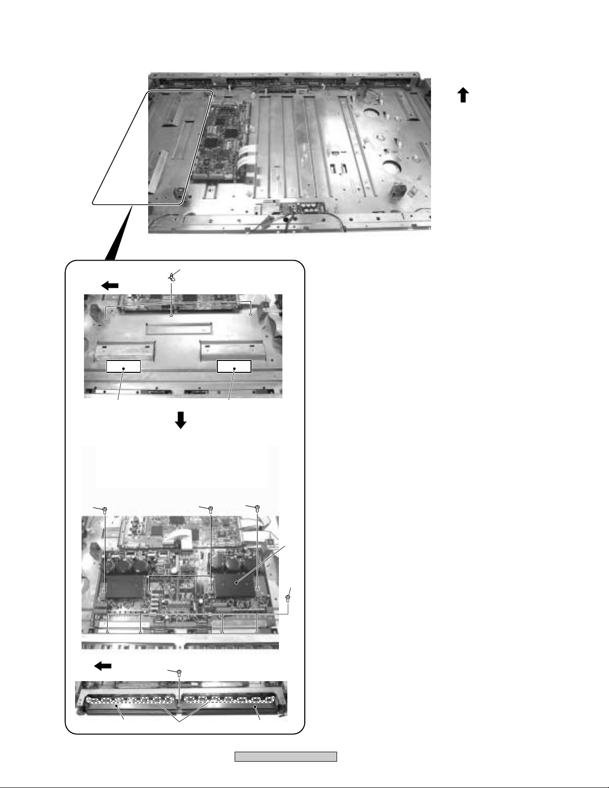
2.6 UNDER LAYER SECTION (5)
Upper side
10
5
4
2
3
10
6
7
7
9
8
7
5
10
6
7
1
10
18
15
11
10 17 10
1413 1214
• Bottom View
18 10
15
11
1414
Wire Saddle
20
19
Fan Jumper
Wire Saddle
16
PDP-433CMX
Page 17

UNDER LAYER SECTION (5) PARTS LIST
•
Mark No. Description Part No.
NSP 2 Heat Sink ANH1594
NSP 6 Metal Fitting ANG2464
NSP 8 PCB Spacer AEC1121
NSP 12 Fan Metal (L) ANG2488
NSP 13 Fan Metal (R) ANG2489
1 THERMAL SENSOR Assy AWZ6696
3 Silicone Sheet AEH1039
4 Rivet BEC1066
5 Insulation Sheet AMR3263
7 Wire Saddle AEC1904
9 Circuit Board Spacer AEC1873
10 Screw ABZ30P060FMC
11 Fan Motor AXM1040
14 Screw PPZ50P100FZK
15 Screw BMZ30P060FZK
16 • • • • •
17 Niplocker AEC1803
18 Fan Label AAX2785
19 J115 3P Housing Wire ADX2780
20 Binder AEC-093
PDP-433CMX
17
Page 18
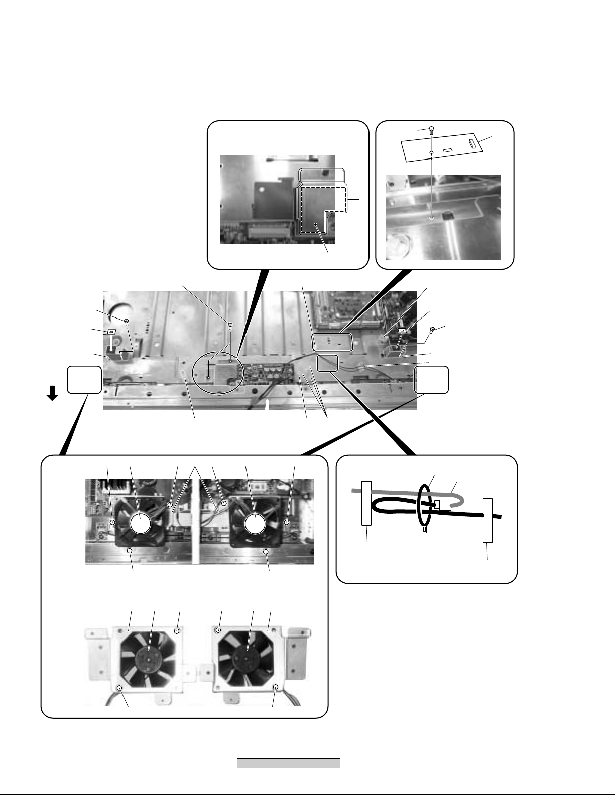
2.7 UNDER LAYER SECTION (6)
Upper side
43
13
15
14
35
37
12
1
27
29
39
27
30
2 10
16
27
5
3
K3
SA2SA1
27 27
31
7
326
4
17
36
TE1
D16
D9
D8
D1
D18
D6
Y1
Y2
D12
46
D13
28
D10
D11
D7
D15
D14
D2
D3
D17
42
25
26
34
45
27
44
20
A5
A1
33
A6 A7
X1
A3
38
18
19
27
40
SA1SA2
K3
18
39
4
24
27
46
8
27 27
3
2223
115
1
21
9
2
PDP-433CMX
Page 19

UNDER LAYER SECTION (6) PARTS LIST
•
Mark No. Description Part No. Mark No. Description Part No.
NSP 1 ADR CONNECT A Assy AWZ6678
NSP 2 ADR CONNECT B Assy AWZ6679
NSP 3 ADR CONNECT C Assy AWZ6680
NSP 4 ADR CONNECT D Assy AWZ6681
NSP 5 ADR RESONANCE Assy AWZ6751
NSP 6 BRIDGE A Assy AWZ6728
NSP 7 BRIDGE B Assy AWZ6729
NSP 8 BRIDGE C Assy AWZ6730
NSP 9 BRIDGE D Assy AWZ6731
10 SUB ADDRESS A Assy AWZ6692
11 SUB ADDRESS B Assy AWZ6693
NSP 12 SCAN (A) Assy AWZ6724
NSP 13 SCAN (B) Assy AWZ6725
14 Y DRIVE Assy AWZ6748
15 DIGITAL VIDEO Assy AWV1971
16 THERMAL SENSOR Assy AWZ6696
NSP 17 X CONNECTOR (A) Assy AWZ6726
NSP 18 X CONNECTOR (B) Assy AWZ6727
19 X DRIVE Assy AWV1985
20 MX AUDIO Assy AWZ6644
21 J209 Flexible Flat Cable ADD1206
22 J210 Flexible Flat Cable ADD1204
23 J211 Flexible Flat Cable ADD1199
24 J212 Flexible Flat Cable ADD1201
25 J201 Flexible Flat Cable ADD1183
26 J202 Flexible Flat Cable ADD1183
27 Flat Clamp AEC1879
28 J203 Flexible Flat Cable ADD1198
29 J205 Flexible Flat Cable ADD1202
30 J206 Flexible Flat Cable ADD1200
31 J207 Flexible Flat Cable ADD1208
32 J208 Flexible Flat Cable ADD1205
33 Power Sheet (43) AMR3284
34 Rivet BEC1066
35 J110 3P Housing Wire ADX2741
36 J108 8P Housing Wire ADX2740
37 J102 Wire PE ADX2738
38 J103 13P Housing Wire ADX2779
39 J116 4P Housing Wire ADX2783
40 J118 Wire L ADX2763
41 J119 13P Housing Wire ADX2768
42 J109 Wire X ADX2787
43 Binder AEC-093
44 J204 Flexible Flat Cable ADD1207
45 J104 Wire W ADX2786
46 J117 4P Housing Wire ADX2783
PDP-433CMX
19
Page 20
2.8 MIDDLE LAYER SECTION (1)
Upper side
Upper side
11
Upper side
12
10
1
5
3
7
11
4
10
11
11
2
10
6
11
12
2
Upper side
11
11
14
MIDDLE LAYER SECTION (1) PARTS LIST
•
8
9
9
14
11
Mark No. Description Part No.
NSP 1 Front Chassis HU (43) ANA1670
NSP 2 Card Spacer AEC1902
NSP 5 Sub Frame L ANG2517
NSP 6 Sub Frame R ANG2518
NSP 7 Front Chassis HL (43CMX) ANA1692
3 Niplocker AEC1803
4 Card Corner Holder BEC1144
20
Mark No. Description Part No.
NSP 8 Front Chassis V (43) ANA1672
PDP-433CMX
15
11
13
9 FPC Cushion (43) AEB1371
10 Screw ABA1283
11 Screw ABA1294
12 Screw BMZ30P060FMC
13 VR Cushion AEB1374
14 V Cushion AED1205
15 Gascket R ANK1695
8
11
Page 21
2.9 MIDDLE LAYER SECTION (2)
11
12
9
4
5
9
MIDDLE LAYER SECTION (2) PARTS LIST
•
3
1
6
Mark No. Description Part No.
7
6
29
12
1 IR Assy AWZ6643
2 MX LED Assy AWZ6642
3 J113 Wire O ADX2778
4 KEY CONNECTOR Assy AWZ6695
NSP 5 IR Holder ANG2494
6 Nyron Rivet AEC1671
7 J111 Wire Y ADX2788
NSP 8 Switch Holder ANG2493
9 Screw BMZ30P040FMC
10 • • • • •
11 V Cushion AED1205
12 Gascket R ANK1695
PDP-433CMX
21
Page 22
2.10 MIDDLE LAYER SECTION (3)
22
3
8
71195 1
J201
Bottom Side
J202
4
RGB Assy
3
5
6
22
6
MIDDLE LAYER SECTION (3) PARTS LIST
•
22
10
23
12
21
22
2
Mark No. Description Part No.
1 RGB Assy AWZ6744
2 SLOT CONNECTOR Assy AWZ6634
3 Spacer AEC1065
NSP 5 RGB Base ANA1662
4 Card Spacer AEC1882
22
12
13
14
6 Ground Finger ANG2468
7 Card Spacer AEC1899
15
17
12
2219
20
18
17
12
11
NSP 18 Video Stay AND1171
NSP 21 PCB Stay AND1170
8 Ferrite Core (L3) ATX1037
9 Ferrite Core Holder AEC1818
10 J112 13P Housing Wire ADX2784
11 Guide Rail EX AEC1900
12 Clamp AEC1884
13 J107 12P Housing Wire ADX2702
14 J109 Wire X ADX2787
15 Nyron Rivet AEC1671
16 • • • • •
17 Wire Saddle AEC1745
19 Ferrite Core (L2) ATX1039
20 Binder AEC-093
22 Screw AMZ30P060FZK
23 Screw VBB30P100FNI
PDP-433CMX
Page 23
2.11 MIDDLE LAYER SECTION (4)
7
7
Upper Rear Side
6
7 7 7
3
6
7
7
1
2
9
10
4
MIDDLE LAYER SECTION (4) PARTS LIST
•
5
4
Upper
Side
Mark No. Description Part No. Mark No. Description Part No.
1 Terminal Panel CMX ANG2486
2 Slot Spring (Under) ABK1028
3 Slot Spring (Upper) ABK1031
4 Card Spacer AEC1898
5 Gascket S ANK1699
6 Screw AMZ30P060FZK
7 Screw TBZ40P080FZK
8 • • • • •
9 Expansion Slot Cover ANG2463
10 Screw BMZ30P060FZK
PDP-433CMX
23
Page 24
2.12 UPPER LAYER SECTION (1)
1
J113
15
16
J201
J201
J201
J202
17
7
14
11
10
J109
12
C3 C1
2
3
17
14
18
2
5
18
15
13
6
4
17
24
PDP-433CMX
Page 25

UPPER LAYER SECTION (1) PARTS LIST
•
Mark No. Description Part No.
1 I/O Assy AWZ6631
2 CONTROL Assy AWZ6633
3 SP OUT R Assy AWZ6706
5 Power Switch (S1) BSM1006
4 SP OUT L Assy AWZ6705
6 AC Inlet with Filter (CN1) AKP1223
7 J201, J202 Flexible Cable ADD1183
8 • • • • •
9 • • • • •
10 J106 Wire C ADX2693
11 Ferrite Core (L1) ATX1032
12 J114 Earth Wire ADX2709
13 J105 Wire B ADX2692
14 Hexagonal Nut ABN1035
15 Hexagonal Head Screw BBA1051
16 Screw PMB30P060FNI
17 Screw BPZ30P080FZK
18 Screw BMZ30P060FZK
PDP-433CMX
25
Page 26
2.13 UPPER LAYER SECTION (2)
VM1
12
10
10
7
4
6
3
9
8
5
P1
P2
P6
P3
P5
P4
P7
26
100V
200V
SW101
1
PDP-433CMX
Page 27
(1) UPPER LAYER SECTION (2) PARTS LIST
Mark No. Description Part No.
1 SW Power Supply Module AXY1059
2 • • • • •
3 J104 Wire W ADX2786
4 J119 13P Housing Wire ADX2768
5 J105 Wire B ADX2692
6 J101 12P Housing Wire ADX2771
7 J118 Wire L ADX2763
8 J103 13P Housing Wire ADX2779
9 J102 Wire PE ADX2738
10 Screw AMZ30P060FZK
11 • • • • •
12 Solder Warning Label See Contrast table (2)
(2) CONTRAST TABLE
PDP-433CMX/LUCB and PDP-433MXE/YVLDK are constructed the same except for the following :
Part No.
Mark No. Symbol and Description
12
Solder Warning Label AAX2644 Not used
PDP-433CMX PDP-433MXE
LUCB YVLDK
Remarks
PDP-433CMX
27
Page 28
2.14 FRONT CASE SECTION
2
4
8
17
10
10
16
16
16
10
18
1
5
6
3
7
PDP-433CMX
Only
16
10
19
(1) FRONT CASE SECTION PARTS LIST
Mark No. Description Part No.
1 SIDE KEY Assy AWZ6637
2 Front Case Assy 43 (M) AMB2712
3 Rivet AEC1877
4 Flexible Seal AEH1036
5 J213 Flexible Cable ADD1195
6 Ferrite Core (L4) ATX1043
7 Lead Cover (MX) AMB2703
8 Pioneer Badge AAM1091
9 • • • • •
NSP 10 Panel Holder (43) ANG2487
11 Spacer AEC1896
12 • • • • •
13 Panel Cushion V (43) AED1201
14 Panel Cushion H (43) AED1200
15 Protect Panel Assy (43) AMR3303
16 Screw ABZ30P050FZK
17 Screw VMZ30P060FZK
18 Energy Star Label AAX2856
NSP 19 Display Label See Contrast table (2)
10
13
16
11
11
10
16
14
14
15
11
11
13
(2) CONTRAST TABLE
PDP-433CMX/LUCB and PDP-433MXE/YVLDK are constructed the same except for the following :
Part No.
Mark No. Symbol and Description
NSP 19 Display Label AAX2836 Not used
PDP-433CMX PDP-433MXE
LUCB YVLDK
Remarks
28
PDP-433CMX
Page 29
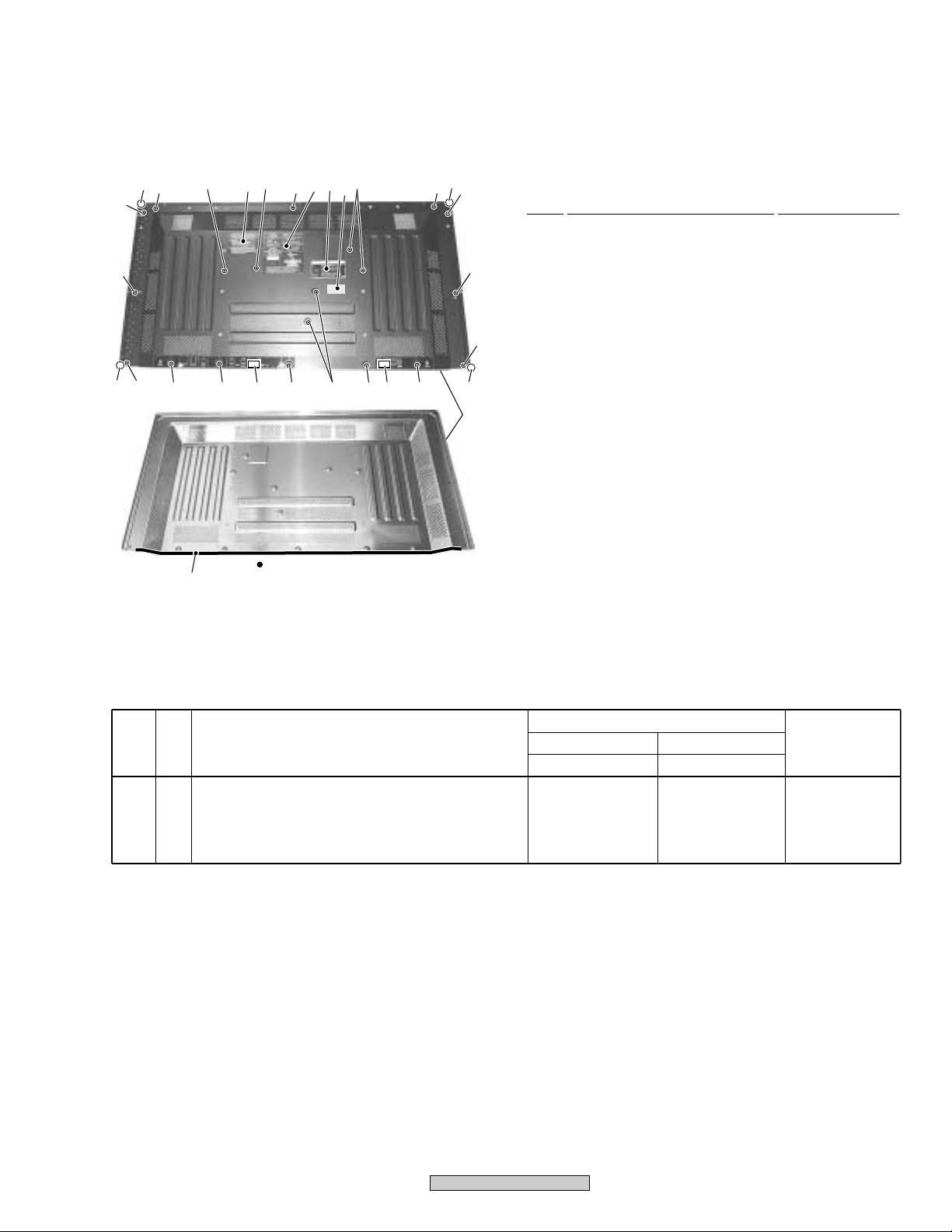
2.15 REAR SECTION
10
10
4
4
4
4
3
2
33 3
5
3 38 93
6
4
Bottom View
7
11
3
10
4
4
4
4
3
10
1
(1) REAR SECTION PARTS LIST
Mark No. Description Part No.
1 Rear Case (M) ANE1601
2 Gascket A ANK1694
3 Screw AMZ30P060FZK
4 Screw TBZ40P080FZK
5 Cleaning Label AAX2751
NSP 6 Name Label See Contrast table (2)
7 Bolt Caution Label AAX2852
8 Terminal Display Label R (43) AAX2878
9 Terminal Display Label L (43) See Contrast table (2)
10 Rear Corner Label AAX2862
11 Korean Label See Contrast table (2)
(2) CONTRAST TABLE
PDP-433CMX/LUCB and PDP-433MXE/YVLDK are constructed the same except for the following :
Part No.
Mark No. Symbol and Description
NSP
NSP66
Name Label (43 CMX)
Name Label (43 MXE)
9
Terminal Display Label L (43) Gray
9
Terminal Display Label L (43E) Gray
11
Korean Label
PDP-433CMX PDP-433MXE
LUCB YVLDK
AAL2430
Not used
AAX2936
Not used
Not used
Not used
AAL2431
Not used
AAX2938
AAX2944
Remarks
PDP-433CMX
29
Page 30
2.16 PDP SERVICE ASSY 433 (AWU1069)
PDP Service Assy 433 (AWU1069) consists of the following parts.
PARTS LIST
•
Mark No. Description Part No. Mark No. Description Part No.
NSP Front Chassis V (43) ANA1702
Panel Chassis (43) Assy AWU1067
NSP Front CHassis HU (43) ANA1698
NSP Front Chassis HL ANA1700
NSP Sub Frame L (43) ANG2517
NSP Sub Frame R (43) ANG2518
Scan IC Spring (43L) ABK1029
Scan IC Spring (43R) ABK1030
NSP Metal Fitting ANG2464
FPC Cushion (43) AEB1371
NSP PCB Spacer AEC1121
Locking Card Spacer AEC1736
Circuit Board Spacer AEC1872
Circuit Board Spacer AEC1873
Spacer AEC1896
NSP Card Spacer AEC1902
Wire Saddle AEC1904
Panel Cushion H (43) AED1200
Panel Cushion V (43) AED1201
V Cushion AED1205
2.17 PANEL CHASSIS (43) ASSY (AWU1067)
Panel Chassis (43) Assy (AWU1067) consists of the following parts.
Insullation Sheet AMR3263
Scan Sheet (43) AMR3287
Card Corner Holder BEC1144
Screw ABA1283
Screw ABA1294
Screw ABZ30P060FMC
Screw BMZ30P060FMC
Screw PMB30P060FNI
Screw VBB30P100FNI
Bolt ABA1259
Corner Pad AHA2293
Upper Carton AHD3139
Under Carton AHD3140
Packing Sheet AHG1291
Washer WB80FZB
VR Cushion AEB1374
Niplocker AEC1803
Static Plate AHK1013
Plate AHK1014
Screw BYC40P220FMC
Washer WC60FZK
Serivec Panel notes ARM1217
PARTS LIST
•
Mark No. Description Part No.
NSP SCAN FUKUGO ASSY AWV1969
NSP ADDRESS FUKUGO ASSY AWV1928
NSP Address Module (IC1 - IC32) AXF1113
NSP FPC (J1,J2) ADY1079
NSP FPC (J3,J4) ADY1080
NSP Chassis Assy (43) ANA1693
NSP Chassis (43) ANA1668
NSP Base Chassis (43) ANA1669
NSP Scan Heatsink (43) ANH1601
NSP Corner Angle A ANG2457
NSP Corner Angle B ANG2458
NSP Tube Cover AMR3262
NSP Plasma Panel Assy (43) AAV1239
Silicone Sheet 43 AEH1043
Adhesive Tape 43 AEH1044
Adhesive Tape B 43 AEH1054
Panel Silicone Sheet AEH1055
Silicone Sheet B 43 AEH1056
Pin Grommet AEC1015
Card Spacer AEC1889
Scan Silicone Sheet (43) AEH1047
Screw VBB30P100FNI
30
LIST OF ASSY
•
Mark No. Description Part No.
NSP SCAN FUKUGO ASSY AWV1969
NSP SCAN (A) ASSY AWZ6724
NSP SCAN (B) ASSY AWZ6725
NSP X CONNECTOR (A) ASSY AWZ6726
NSP X CONNECTOR (B) ASSY AWZ6727
NSP BRIDGE A ASSY AWZ6728
NSP BRIDGE B ASSY AWZ6729
NSP BRIDGE C ASSY AWZ6730
NSP BRIDGE D ASSY AWZ6731
NSP ADR CONNECT A ASSY AWZ6678
NSP ADR CONNECT B ASSY AWZ6679
NSP ADR CONNECT C ASSY AWZ6680
NSP ADR CONNECT D ASSY AWZ6681
PDP-433CMX
ADDRESS FUKUGO ASSY AWV1928
ADR RESONANCE ASSY AWZ6751
Page 31

Caution in Replacement of Chassis Block
Please order the PDP Service Assy 433 (AWU1069) when replacing the Chassis block.
PDP Service Assy 433 is all common use parts of for business, public use and module.
Supply it by the state that installed Circuit Board Spacer (AEC1872) and Wire Saddle (AEC1904) as follows.
Therefore need to remove it in accordance with model.
Confirm character carved a seal near the parts, and remove it.
P : Public exclusive use
W : Module exclusive use
PW : Common use of public use and module
∗ In case of this unit, the parts that "W" is marked removes.
PDP Service Assy 433 (AWU1069)
Circuit Board Spacer
(AEC1872)
PDP-433CMX
Circuit Board Spacer
(AEC1872)
31
Page 32

1
23
3. BLOCK DIAGRAM AND SCHEMATIC DIAGRAM
4
A
3.1 BLOCK DIAGRAM
3.1.1 OVERALL BLOCK DIAGRAM
DriverICDriver
ADR CONNECT A
ASSY
B
SCAN (A) ASSY
(UPPER)
IC5
VCC_VH
IC6201
ADD
PSUS
SEL_PULSE
IC5
VCC_VH
IC6202
ADD
SIDE KEY
ASSY
SW1
RE1
IR ASSY
SEL_PULSE
IC5
VCC_VH
IC6203
ADD
SEL_PULSE
IC5
VCC_VH
IC6204
ADD
SEL_PULSE
IC5
VCC_VH
IC6205
ADD
SEL_PULSE
IC5
VCC_VH
IC6206
ADD
SEL_PULSE
SCAN (B) ASSY
(LOWER)
SEL_PULSE
SEL_PULSE
SEL_PULSE
SEL_PULSE
SEL_PULSE
SEL_PULSE
KEY CONNECTOR
ASSY
IC5
IC6001
ADD
IC5
IC6002
ADD
IC5
IC6003
ADD
IC5
IC6004
ADD
IC5
IC6005
ADD
IC5
IC6006
ADD
VCC_VH
SCAN
VCC_VH
VCC_VH
VCC_VH
VCC_VH
VCC_VH
SCAN
PSUS
KL1 KL2
ADR CONNECT D
ASSY
SPR1
ROUT
SP OUT R
ASSY
C
D
E
F
DriverICDriver
IC
AA1
Y DRIVE ASSY
Y4
PSUS
VCC_VH
V_IC5V
Y3
VCC_VH
V_IC5V
Y5
PSUS
Y6
SR IN SR OUT
CONTROL ASSY
AD1
IC
DriverICDriver
IC
CLK/LE
IC6501
Buffer IC
VC_VF+ VC_VF- V_OFS VCC_VH V_IC5V
+5V +15V
Pulse Module
+15V VSUS
+Reset Block
+5V +15V VSUS
Pulse Module
VC_VF+
Photo Coupler
DC/DC Conv.
IC2206
IC2204
+15V
Soft-D
Block
VC_VF- V_OFS
Offset
Block
V_IC5V
Block
VCP
Y-SUS
MASK
Block
VCP
Y-SUS
MASK
Block
Scan Signal
C3
232C
DRIVER
CombiINCombi
CLK/LE
OUT
IC6901
Buffer IC
RS-232C
THERMAL
SENSOR
ASSY
Block
VSUS
BRIDGE C
ASSY
Drive
Signal
Drive
Signal
C1
DriverICDriver
BGA1
BRIDGE A
ASSY
+5V
Logic
Block
BGC1
IC
TE1
VADR2
Y1
Y2
VADR2
DriverICDriver
IC
VADR2
CLAMP
ADR CONNECT B
ASSY
AB1
D8 D9 D16
D1
+12V
V+5V_STB
+12V
D18
D6
ADL_LE_DR
+12V
V+3V
IC1703
XY Drive
Sequence Pattern
Gen.
YDRV_SIG
SCAN_SIG
V+3V_I
V+2V_I
IC1401 (IC31 R)
Sub-Field Conv.
for Right with Field Memory
ADCLK_DR
V+5V_STB
TXD/RX
IC1207
Module
UCOM
DC/DC Conv.
Module
DIGITAL VIDEO
ASSY
KL_U0:2
XDRV_SIG
ADL_LE_UL
ADL_LE_DL
V+3VD
X180
Clock
Gen.
IC1301 (IC31 L)
Sub-Field Conv.
for Left with Field Memory
V+3VD
IC1101
Panel UCOM
D13D12
CLAMP
VADR2
ADR CONNECT C
ASSY
AC1
Driver
Driver
IC
IC
ADR RESONANCE
ASSY
V+5VD
V+3VD
V+2VD
V+3V_IC
V+2V_IC
V+3VD
IC1191
Flash
ROM
ADR RESONANCE
ASSY
DriverICDriver
IC
CLK/LE
IC6601
Buffer IC
SUB ADDRESS A
ASSY
D10
D11
V+2V
V+3V
V+5V_STB
D15
D14
D2
BA2:9
BB2:9
GA2:9
GB2:9
RA2:9
RB2:9
TXD0/RX0
RE
LED_SIG
I2
D3D17
SUB ADDRESS B
ASSY
IC6801
Buffer IC
CLK/LE
DriverICDriver
K2
K1
SAA3
+60
SAA1 SAA2
D7
D4
SAB1 SAB2
+60
SAB3
K1
K2
IC
VADR2
Q6706 - Q6711
VADR Gen.
ADR_CO
ADR_CO
Q6706 - Q6711
VADR Gen.
VADR2
32
DriverICDriver
DriverICDriver
IC
IC
DriverICDriver
IC
DriverICDriver
IC
DriverICDriver
IC
DriverICDriver
IC
DriverICDriver
DriverICDriver
IC
IC
PDP-433CMX
1234
Page 33

5
678
Note : When ordering service parts, be sure to refer to "EXPLODED VIEWS and PARTS LIST" or "PCB PARTS LIST".
DriverICDriver
IC
VADR2
SW POWER SUPPLY MODULE
SW POWER SUPPLY Block
+13.5V
-9V
R2
BA29
BB29
GA29
GB29
RA29
SD RAM
10M
RB29
R3
+3V,+5V,-5V,+9V
SD RAM
10M
RGB ASSY
T4 T1 T5 T2 T6 T3
12V,9V,±5V,3V
Reg
Plug&Play
E2PROM
DriverICDriver
IC
ADR CONNECT C
ASSY
AC1
DriverICDriver
CLK/LE
DriverICDriver
IC6801
Buffer IC
IC
IC
K3
T105T105T104T103
LIVE
NEUTRAL
RC101
PRIMARY
SECONDARY
POWER (RELAY)
VSUS
+13.5V
-9V
+6.5V
+13.5V
+6.5V
+15V
+12V
STB5V
-9V
T101
Switching
T102
+12V
Q115
Switching
Q117
STB5V
Switching
Q119
VADR
Switching
VSUS_CONT
+15V
M111
Q112
M114
STB5V
P1 P2 P5 P6 P3 P4
IC5301
(IC30)
SD RAM
10M
IC5102
(IC101)
SD RAM
10M
12V,13.5V,
9V,±5V,
-9V,6.5V,
3V
STB5V
13.5V,6.5V,-9V
I/O ASSY
Component/
RGB
INPUT1 INPUT2
STB+5V+3V,+2V
OUTPUT
3State
Buffer
IC5001
(IC102)
IN1 DET
IC5601
WIDE
UCOM
A/D PLL AMP
R6
12V,
STB5V
SEL SEL
Component/
IC4603
RGB
R9R4
Flash
ROM
12V,13.5V,
-9V,6.5V
R1
STB+5V
IC5505
MAIN
UCOM
MATRIX
6M LPF
S1
SLOT CONNECTOR
ASSY
STB5V
AudioINAudio
INPUT1/2/5
S3
OUT
STB+5V
12.5V
I2C-BUS
S2
Plug & Play
E2PROM
R8
IC4803
PLD
for SYNC
+3V,+5V,-5V
+3V,+5V
Reg
Reg
3State Buffer
Receiver
VADR2
VADR2
CLAMP
BGB1
BRIDGE B
ASSY
V MID CLAMP Block
RL101
LIVE
VSUS
NEUTRAL
+15V
MX AUDIO ASSY
+5V_AD/RGB
OP-Amp
FAN_NG
Temp3
Audio_NG
A5
+15V,+5VSTB
R_Audio
Audio
L_Audio
Mute
A_Mute2
A1
V1
+7V,-8V
+7V
IC7401
TMDS
DVI-D Audio Audio OUTPUTCompositeS-Video
INPUT5
Chroma Decode (4-ISEL)
SECAM
FLT
SEL SELIN3 DET IN4 DET
INPUT3 INPUT4
DriverICDriver
VM1
P7
FAN_Mute
(Buf)
Power Amp
IC7302
6M LPF
3L Y/C
6M LPF
IC
ADR CONNECT D
ASSY
CLAMP
CLAMP
AC IN
D.C Det
+15V
IC8601
VIDEO SLOT
ST1 ASSY
I2C-BUS
6M LPF
3D Y/C
& CNR
DriverICDriver
+15V
IC8701
Regulator
E2PROM
SD RAM
+5VSTB
ROUT
LOUT
A3
Expander
IC
DriverICDriver
IC
AD1
CLK/LE
DriverICDriver
IC6901
Buffer IC
IC
X DRIVE ASSY
X1
+5V
+15V
VSUS
DC/DC
Conv.
Block
Drive
Signal
+5V
Logic
Block
A6
X2
Drive
Signal
A7
L1
MX LED
ASSY
SP OUT L
SPL1
ASSY
L OUT
IC3200
Pulse
Module
+Reset
Pulse
Block
+5V
IC3201
Pulse
Module
VCP
X_SUS
MASK
+15VV_RN
+15VVSUS
VCP
X_SUS
MASK
X3
P_SUS
P_SUS
X4
A
B
X CONNECTOR (A) ASSYX CONNECTOR (B) ASSY
C
D
E
VADR2
DriverICDriver
K3
ADR CONNECT B
ASSY
IC
5
DriverICDriver
BRIDGE D
ASSY
BGD1
AB1
IC
DriverICDriver
IC
CLK/LE
IC6601
Buffer IC
DriverICDriver
IC
6
CLAMP
VADR2
VADR2
DriverICDriver
IC
PDP-433CMX
ADR CONNECT A
ASSY
DriverICDriver
IC
7
AA1
DriverICDriver
IC6501
Buffer IC
CLK/LE
IC
DriverICDriver
IC
F
33
8
Page 34

1
23
4
A
B
C
D
3.1.2 RGB ASSY
I/O ASSY
13.5V
6.5V
-9V
STB+5V
IC4110
(24LCS21A)
SW
Plug&Play
ROM
(LT1399CS)
Video
Amp.
(TC74VHC541)
WP_SW
INPUT1
Component
/RGB
INPUT1
Monitor
Out
INPUT2
Component
/RGB
Terminator
SW
IC4004
V+12V V+12V
IC4002
V+9V V+9V
IC4003
V+5V V+5V
IC4005
V+3.3V V+3.3V AD
IC4006
V+3.3V V+3.3V PLD
IC4001
V-5V V-5V
STB+5V
Time
3CH
TTL
Conv.
Circuit
INPUT1
Input DET.
IN1DET
IC4108
(BA7657F)
RGB
2-1 SW
IPKILL(68)
CS(67)
FILM(70)
HWR(66)
RD(65)
RES(62)
Analog RGB HV / YPbPr
UD[8:15]
Digital RGB
IC5102
(PE5066ACK)
IC101
UA[0:20]
YI[0:7]
PBI[0:7]
YI[0:7]
PBI[0:7]
CLP1(278)
CLP2(279)
HBLK1(280)
VBLK1(282)
HOLD
CLP_AMP
CLP_AMP
CBLK_MAT
CLP_MAT
CBLK_LPF
PR[0:7]
PR[0:7]
VD_AD(53)
YP[0:15]
PBP[0:15]
PRP[0:15]
YP[0:15]
PBP[0:15]
PRP[0:15]
IC5001
(???????)
IC102
HI(57)
VI(58)
VI(167)
HI(168)
FI(64)
HP(55)
VP(56)
FI(166)
VP(169)
HP(170)
HD_AD(52)
(103)
DIVOUT
HOLD(106)
SYNCIN(111/112)
CLPIN(113)
CLK(236)
CLK(3)
RA_IP[0:7]
GA_IP[0:7]
BA_IP[0:7]
SCP-IN
(31)
6M LPF
RAO[0:7]RBO[0:7]
GAO[0:7]GBO[0:7]
BAO[0:7]BBO[0:7]
FDET(60)
VACT(61)
WAIT(62)
EMG_IP(67)
IC4603
(CXA3516R)
A/D PLL AMP
(2-1 Select)
ACL AMP
IC4402
(CXA2101AQ)
MATRIX ~35M
(3-1 Select)
SD RAM
16M
SD RAM
16M
CS(66)
HWR(64)
RD(65)
RES(56)
G/YOUT(2)
B/CbOUT(1)
R_CrOUT(3)
ACL
GeonSYNC(1)
GeonSYNC(2)
(LCX125)
CLK SEL
XUNLOCK
(104)
SDA(56)
SCL(55)
(101)
1/2CLK
EXT_INT
2-1
SEL
DIVOUT(32)
HD_30(72)
HD_PLL(27)
VD_AD(8)
HD_RGB(41)
VD_RGB(42)
HD_PLK2(117)
VD_PLK2(116)
HD_PLD(119)
VD_PLD(118)
CLP1(5)
CLP2(6)
HBLKT(7)
VBLKT(8)
VCLK(132)
DEO(99)
HDO(98)
VDO(97)
(LCX541)
Selector
Buffer
2-1
Circuit
SYNC SEP
VD_SEP(107)
HD_SEP(106)
CLP_AMP(28)
CLP_MAT(111)
CBLK_MAT(110)
CBLK_LPF(109)
HDLD_PLL(31)
VPOL(97)
HPOL(98)
HSTATE(96)
CLP_SEP(99)
-HS(100)
+HS(101)
+VS(102)
Clamp
SW
VSTATE(93)
CLP_SW1(91)
CLP_SW2(92)
Terminator
IC4103
Mute
A_MUTE1
(TC4052BF)
EXT/INT
SEL
EXT_INT
(TC4052BF)
FIX/VAL
IC4103
SEL
FIX_VAR
E
Audio
Input
Audio
Output
Audio Amp.
IC4104
(TA7630P)
Pre-Amp.
VOL
A_MUTE2
AUDIO_NG
Audio
Input A
2-1
SEL
Audio
Input B
(LCX541)
Line Buffer
(TFP201H)
TMDS RECEIVER
DVI
2-1
SEL
VIDEOINVIDEO
Y/C
LPF
OUT
Chroma Decode (4-1 Select)
SECAM
FLT
6M LPF
3L Y/C
6M LPF
3D Y/C&CNR
SD RAM
I2C BUS
3D_RST
6M
DVI_PS
VY_SBL
Expan.
DBR
F
34
PDP-433CMX
1234
Page 35

MCLKI(242)
RAI[0:7]RBI[0:7]
GAI[0:7]GBI[0:7]
BAI[0:7]BBI[0:7]
CLKI(286)
HDI(297)
DEI(296)
VDI(299)
HIS(300)
SD RAM
16M
OSD_RXD(21)
5
SD RAM
16M
OSD_CLK(22)
OSD_CE(23)
HWRB(301)
RDB(302)
RESETB(303)
HWR_30
IC5301
(PD6357B)
IC30
CS4B(1)
CS_30(66)
IC_RST(126)
RDB(91)
HWRS(92)
SGLB_AD(79)
DLK_PLL(105)
PLL_OE(33)
TXD_WU(97)
SCK_WU(101)
HWR_DLAY
CLKOUT(88)
CLK2A(247)
MCLKO(152)
H(119)
DEO(92)
HDO(91)
VDO(90)
VI(31)
FI(118)
RA[0:9]RB[0:9]
GA[0:9]GB[0:9]
BA[0:9]BB[0:9]
HD_W(117)
VD_W(34,73)
DE_W(33,72)
100MHz
X'tal
OSDH(62)
OSD_V(49)
WACT_FRCT(32)
φ(88)
678
A
DIGITAL VIDEO
ASSY
RGB ASSY
IC31
(1/2)
(MEM29L800TA-90PFIN)
UA [0 : 20]
UD [0 : 15]
IC5601
(HD64F2328VF)
Wide UCOM
D_CLK(63)
D_RXD(61)
IC5602
Flash ROM
RY/BY(102)
WU_CE(29)
CS_FLASH(69)
A13_FLASH(70)
WAIT_FLASH(102)
FEW_CE(60)
MD2(125)
RST IC
EXT_RXD(62)
EXT_TXD(60)
AND
RESET(61)
REQ_WU(71)
D_BUSY(64)
VD Shift
V+3VD
V+2VD
DC/DC
Converter
IC31
(2/2)
B
C
ULK_PLL(30)
IC4803
(EPM3256ATC144-10)
PLD for SYNC
HD_U(140)
VD_U(139)
IN4DET IN3DET EEPROM
CLK(125)
FR_SEL(134)
PLD_CE(137)
SCK(128)
TXD(138)
H_POL_U(132)
V_POL_U(131)
SYNC_ST(136)
Slot
State
IC5503
(TC74WHTC541AFT)
5V → 3.3V Converter
Wide UCOM Write Connector
IC5504, IC5509
(74HCT00)
SYNC SEL
DIN_SEL
(66)
ACL_SW(58)
SCL(29)
SDA(30)
SIGRST(88)
FR_SEL(51)
PLD_CE(90)
TXD(1)
CLK(2)
H_POL(79)
V_POL(80)
SYNC_ST(85)
SLOT_ST(93)
SLOT_ST2(22)
RGB_SEL(52)
IN1DET(40)
IN3DET(36)
IN4DET(37)
(45)
OSD_CE
DPMS(7)
WU_CE(47)
H_SYNC(5)
FWE(68)
WP_SW(21)
VOL(4)
EXT_INT(76)
FIX_VAR(84)
A_MUTE1(77)
A_MUTE2(78)
SDIN_SEL(67)
H_SYNC(6)
AUDIO_NC(42)
(E)SDA(82)
IC5502
(24LC64(I)SN
EEP ROM
MD2(69)
(E)SCL(81)
EEPRST(83)
THERMO
SENSOR
WE_WU(71)
RST_WU(70)
IC5505
(M3062FGAFP)
Main UCOM
TEMP(94)
FAN_NG(48)
FAN(3)
FAN KEY LED RS-232C REM
SLOT CONNECTOR ASSY
IC5501
(TC74WHTC541AFT)
3.3V → 5V Converter
TC7W126FU
BUSY(54)
IN5DET(49)
REQ_WU(74)
KEY1_SCAN(20)
LED_G(37)
LED_R(38)
Main UCOM
Write Connector
RST2(75)
BUSY30(55)
PNL_MUTE(60)
CNVSS(9)
BUS(34)
RXD1(32)
(M5223)
OP AMP
TXD0(35)
RXD0(36)
WE_MD(72)
POWER(53)
REQ_MD(19)
REM(18)
CB_MUTE
TXD1(31)
RST(12)
(PS9248N)
TEMP2(95)
(50)
RST IC
(LM50C1M3)
Thermo
Sensor 2
TC7W126FU
D
Module UCOM
E
VIDEO SLOT ST1 ASSY (OPTION)
5
6
PDP-433CMX
F
35
7
8
Page 36

1
23
4
A
B
C
D
3.1.3 DIGITAL VIDEO ASSY
RGB ASSY DIGITAL VIDEO ASSY
RGB 2 phase 10 bit
Reflesh-rate
Det.
AND
WE_PN
Line
Buffer
IC5301
(PD6357)
IC30
IC5505
(M30624FGAGP)
Main
Microcomputer
VD
HD
DE
CLK
RXDO
REM
PM_ST
PN_MUTE
CN1201
MAX_PLS1
DITHER
MOD_SW
POWER
MAX_PLS2
TXDO
REQ_MD TXDO
EXT_RXD
EXT_TXD
RXDO
3.3V
3.3V
Flash ROM
HD
VD
RESET
EXD RXD
EXD TXD
RESET
Reset IC
Address BUS
Data BUS
Control Signal
IC1191
3.3V
Panel Microcomputer
RST PU
(M30624FGAFP)
Module Microcomputer
TEMP1
THERMAL
SENSOR
Assy
3.3V
2.5V
VD 31
IC1101
(HD64F2328VF)
3.3V → 5.0V5.0V → 3.3VReset IC
IC1207
AC_OFF
PD_TRIGGER
IC1301 (IC31 L)
(PD6358)
DRAM
IC1401 (IC31 R)
(PD6358)
DRAM
3.3V
APLR
RXD
BUSY
REQ_PU
RST2
IC1703 (IC23)
(PE5064)
Address
Resonance
STOPB
Control
PC_VIDEO
ADR_K_EMG
AND
APD MUTE
STB5V
RELAY
Address Data
Address Data
Sustain
Control
5V
OR
ADR K PD U
ADR K PD D
Panel W/B ADJ.
Hour/Pulse meter
DEW DET
STB5V
ADR PD
IIC BUS
EEP
ROM
DCC_PD
5V
OR
DIG. ADR. PD
SW POWER SUPPLY Module
ADR CONNECT A - D
Assy (Left section)
ADR CONNECT A - D
Assy (Right section)
Y DRIVE Assy
X DRIVE Assy
RESONANCE
Assy
pn
5V
3.3V
2.5V
DC/DC
Converter
Block
12V
STB5V
STB5V
E
F
36
PDP-433CMX
1234
Page 37

1
23
21
5
7
9
11
13
15
17
19
PN_MUTE
XNR-U
XSUS-B
XSUS-U
XSUS-D
XSUS-G
XSUS-MSK
XCP-MSK
XNR-D1
XNR-D2
CN3001
X2
1
2
3
4
8
11
CN3101
X1
XNR_U
XNR_U
2
4
5
3
6
6
5
2
3
4
9
IC3004
TC74ACT540FT
IC3008
TC74ACT541FT
18
17
14
14
15
18
17
16
16
15
1
5
2
3
4
6
8
9
7
10
IC3008
PE1012A
20
23
22
21
19
17
16
18
15
2
3
4
5
7
8
6
9
IC3001
TC74ACT541FT
IC3102
HCPL-M611
IC3101
TC74ACT541FT
IC3200
STK795-460
Pulse Module
IC3201
STK795-460
Pulse Module
T3701
VRN D-D CONV.
XCP-MSK
XSUS-MSK
VCP
PLD
SUSOUT A
37-40
29,30
K3105
PSUS
K3107
IC3103,IC3104
TND301S
Q3103 Q3104,
Q3109
Q3105,
Q3124
Q3106,
Q3125
SUSOUT B
37-40
29,30
K3106
IC3106,IC3107
TND301S
Q3110,
Q3114
Q3111 Q3112,
Q3126
Q3113,
Q3127
To
X CONNECTOR
ASSY
IC3110
TND301S
IC3113
TND301S
charge pump
circuit
From DIGITAL VIDEO ASSY
Photo
coupler
2-9 11-18
+15V
DGND
XDRIVE_PD
XDC_DC_PD
VSUS
SUSGND
SUSGND
SUSGND
P.D.
DET.
18
17
16
15
13
12
14
11
14
16
18
20
14
16
18
20
VSUS 225V
VRN UVP
VRN OVP
Q3116
Q3120
Q3122
Q3128
XNR-D1
XNR-D2
VRN-300V
234
3.1.4 X DRIVE ASSY
A
B
C
D
E
1
PDP-433CMX
2
3
37
4
F
Page 38

1
23
4
A
3.1.5 Y DRIVE ASSY
CLR
27
CLK
25
OC1
LE
AB
SI1
SI2
30
31
40
42
43
45
IC2001
TC74ACT541FT
OC2-1
B
OC2-2
Photo Coupler
Photo Coupler
Photo Coupler
Photo Coupler
Photo Coupler
Photo Coupler
IC2501,IC2502,
IC2505,IC2510,
IC2512,IC2513,
IC2514,IC2525,
HCPL-M611
TC74ACT540FT
Photo Coupler
IC2516
HCPL-M611
IC2504
TC74ACT540FT
IC2506
TC74ACT540FT
IC5V
VH
IC2503
VH
Y5
To SCAN ASSY
(Lower)
CN2501CN2502
To SCAN ASSY
(Upper)
Y3
GNDH
Pulse Module
YCP-MSK
YPR-U2
YSUS-MSK
14
(STK795-460)
16
18
20
Pulse Module
14
(STK795-460)
16
18
20
charge pump
IC2206
IC2214
circuit
Photo Coupler
IC2202
HCPL-M611
Photo Coupler
IC2208
HCPL-M611
C
+13.5V
SUS muteDET.
circuit
IC2005
33
24
19
21
9
10
12
18
13
16
15
22
46
Y2
TC74ACT541FT
IC2007
TC74ACT540FT
Q2102
IC2006
PE1013
Dew DET.
OC2-2
PN_MUTE
YPR-U1
YPR-U2
YSUS-B
YSUS-U
YSUS-D
D
YOFS
YSUS-G
YCP-MSK
YSUS-MSK
YSOFT-D
DEW_DET
circuit
Vsus
E
1
+15V
-9V
VSUS
VSUS
2
3
4
5
6
7
10
11
13
14
SUSGND
D. GND
D. GND
+13.5V
YDRIVE_PD
YDC_DC_PD
VOFS_ADJ
SUSGND
SUSGND
F
P.D.
DET.
IC5V UVP
VOFS UVP
VOFS OVP
VH UVP
VH OVP
IC5V, VF
D-D CONV.
VOFS D-D
VH D-D CONV.
-9V
IC2004
TC74ACT541FT
IC2005
TC74ACT541FT
CONV.
YPR-U1
YSOFT-D
YOFS
IC5V
VF+
VF-
VOFS
VH
38
1234
PDP-433CMX
Page 39

5
678
A
YPR-U1
YPR-U2
SUSOUT A
37-40
29,30
5V
15V
Vsus
SUSOUT B
37-40
29,30
5V
15V
Vsus
VSUS
IC2203
TND301S
K2203
K2212
VCP
IC2212
TND301S
Q2218
IC2213
TND301S
Q2220
IC2216
TND301S
Q2226
IC2217
TND301S
Q2232
Q2204
Q2219
Q2221
Q2217
Q2233
Q2215
Q2227
Q2205
K2220
PSUS
TO
Y CONNECTOR
ASS'Y
B
C
D
5
IC2201
TC74ACT541FT
2-9
11-18
IC2204
TND301S
IC2210
TND301S
6
Q2210
SUSGND
Q2211
PDP-433CMX
PSUS
E
F
39
7
8
Page 40

1
[ FAN Drive Block ]
[ MX Audio Block ]
+15V
+15V
+5VSTB
R_Audio
GND
A_Mute
Stand_by
GND
L_Audio
R_Audio
L_Audio
+5VSTB
R_OUT
R_GND
L_GND
L_OUT
Temp3
POWER AMP
IC8601
+15V
+5VSTB
D.C
Detect
FAN_PD
FAN_D
FAN_PD
FAN_D
+15V
Vin Vout
Vc Vadj
FAN_Mute
( < 3.4V )
REGULATOR
IC8701
+5V_AD/RGB
Audio_NG
Temp3
FAN_NG
uCOM_FAN
OP-AMP(Buf)
+5V_AD/RGB
+5V_AD/RG
B
NOR
(3.06V - 1.66V)
Audio
Mute
A5
A1
A6
A7
A3
23
4
A
B
3.1.6 MX AUDIO ASSY
C
D
E
F
40
1234
PDP-433CMX
Page 41

1
234
3.1.7 SUB ADDRESS A and B ASSYS
+60V
ADRGND
CN8801
H : V MID CLAMP OFF
L : V MID CLAMP ON
V MID SW
ADRK EMG1
+12V
DGND
ADR-B ADR EMG 1 Block
ADR-U
ADR-D
ADRK. PD
CN8802
(DC+AC) (-AC) 5V
Current - Voltage
Convert Block
R8801 - R8805 Q8801
P.D. Output Block
Q8803, Q8831 Q8805, Q8806
BUFF Block
IC8801 IC8801 D8804
Inversion
Block
Over Current DET. Block
ADR Output
Resistance Load Block
12V
+5V REG
A
B
C
SW
ADR-D
ADR-U
ADR-B
+12V
DGND
VADR
ADRGND
ADROUT
CN8803
H : EMG1 OFF
L : EMG1 ON
Conparator
Additional
Block
IC8802 IC8802 IC8803
(DC) CLK
(EMG : ON)
Conparator
(EMG : OFF)
IC8804
CLR
Flip / Flop
D
E
F
PDP-433CMX
1
2
3
4
41
Page 42

1
23
4
A
3.1.8 ADR RESONANCE ASSY
CAUTION :
FOR CONTINUED PROTECTION AGAINST RISK OF FIRE.
+60V
+60V
+60V
+60V
CN6702 IC6704 C6703 - C6708
12V
ICP-S1, 0
REPLACE ONLY WITH SAME TYPE NO. ICP-S1.0 MFD
BY ROHM CO., LTD. FOR IC6704.
B
ADROUT
ADRGND
VADR
ADR-B
Pre-Drive
ADR-B
Drive
C6720 Q6706
DGND
+12V
ADR-B
IC6701 Q6701, Q6704 ADR U
C6721 Q6708
ADR-U
Address Resonance Output Block
ADR B
Q6707
Q6709
ADR-D
SW
CN6701
C
ADR-U
Pre-Drive
IC6702 Q6702, Q6705
ADR-U
Drive
ADR OUT
L6704
VADR
V MID
ADRGND
DGND
SW
CN6703
DGND IC6703 Q6703, Q6712 V MID
D
ADRGND
ADR-D
Pre-Drive
ADR-D
Drive
C6722 Q6710
ADR D
Q6711
C6716
C6718
3.1.9 ADR CONNECT A, B, C and D ASSYS
Address Module
(TCP)
E
DATA_R
DATA_G
DATA_B
DATA_R
DATA_G
DATA_B
F
42
1234
Address Module
(TCP)
DATA_R
DATA_G
DATA_B
DATA_R
DATA_G
DATA_B
Address Module
(TCP)
DATA_R
DATA_G
DATA_B
PDP-433CMX
DATA_R
DATA_G
DATA_B
Address Module
(TCP)
DATA_R
DATA_G
DATA_B
DATA_R
DATA_G
DATA_B
CN6501
ADR PD
HZ
LBLK
HBLK
LE
CLK
HZ
LBLK
HBLK
LE
CLK
ADR OUT
BRIDGE ASSY
OPEN PD
Q6502, Q6503
Buffer
IC6501
Page 43

1
234
3.1.10 VIDEO SIGNAL ROUTE
IC5301
IC5001
IC4603
PD6357B
PE5067A-K
CXA3516R
IC5301
PD6357B
IC5001
PE5067A-K
IC4603
CXA3516R
IC5301
PD6357B
IC5001
PE5067A-K
IC4603
CXA3516R
IC5301
PD6357B
IC5001
PE5067A-K
IC4603
CXA3516R
IC5301
PD6357B
IC5001
PE5067A-K
IC4603
CXA3516R
IC5301
PD6357B
Analog Video Signal
Digital Video Signal
A
B
C
IC4402
CXA2101AQ
IC4403
6M LPF
IC4108
BA7657F
(480i)
VIDEO Signal
IC4402
CXA2101AQ
IC4108
BA7657F
(except 480i)
VIDEO Signal
IC4108
BA7657F
PC Signal
IC4402
CXA2101AQ
(NTSC etc.)
VIDEO Signal
IC7401
TFP201A
PC Signal
INPUT1
IC4108
BA7657F
IC4403
6M LPF
INPUT2
IC4402
CXA2101AQ
VIDEO SLOT
INPUT3/4
D
E
INPUT5
INPUT Input Signal Signal Route
1
1/2
F
3
Total Figure
43
4
3/4
5
PDP-433CMX
2
Page 44

1
23
4
A
3.1.11 SYNC SIGNAL ROUTE
IC5301
PD6357B
IC5301
PD6357B
IC5301
PD6357B
IC5301
PD6357B
IC5301
PD6357B
IC5301
PD6357B
IC5301
PD6357B
Analog Video Signal
Digital Video Signal
B
IC5001
C
IC4803
PE5067A-K
PDY077
IC5001
PE5067A-K
IC4803
PDY077
IC5001
PE5067A-K
IC4803
PDY077
IC5001
PE5067A-K
IC4803
PDY077
IC5001
PE5067A-K
IC4803
PDY077
IC5001
IC4803
PDY077
PE5067A-K
IC4802
M52346SP
IC4802
M52346SP
IC4802
M52346SP
IC4802
M52346SP
D
IC4801
NJM2234
IC4108
BA7657F
IC4108
BA7657F
This circuit that
separates with VD
from CompositeSYNC
IC4108
BA7657F
IC4801
NJM2234
IC4108
BA7657F
IC4801
NJM2234
E
INPUT2
INPUT3/4
VIDEO SLOT
INPUT5
GonSYNC/YonSYNC
Composite SYNC
Separate SYNC
GonSYNC/YonSYNC
Separate SYNC5Separate SYNC
INPUT1
(+DE, +CLK)
F
INPUT Input Signal Signal Route
1/2
44
3/4
PDP-433CMX
Total Figure
1234
Page 45

3.2 WAVEFORMS
RGB ASSY
CH1 : IC5505 - pin 29 (SCL)
1
CH2 : IC5505 - pin 30 (SDA)
V: 5V/div. H: 500µsec/div.
CH1 : IC5505 - pin 1 (TXD)
6
CH2 : IC5505 - pin 2 (CLK)
V: 5V/div. H: 100µsec/div.
CH1 : IC5505 - pin 81 ((E) SCL)
2
CH2 : IC5505 - pin 82 ((E) SDA)
V: 5V/div. H: 500µsec/div.
IC5505 - pin 20 (KEYSCAN)
3
V: 5V/div. H: 50msec/div.
CH2
CH1
CH2
CH1
CH2
GND
GND
CH1
CH2
GND
GND
CH1
GND
GND
GND
GND
GND
IC5505 - pin 15 (XIN)
7
V: 2V/div. H: 50nsec/div.
CH1
CH2
CH1
CH2
GND
GND
GND
GND
GND
IC5505 - pin 35 (TXDO)
4
V: 5V/div. H: 1msec/div.
IC5505 - pin 18 (REM)
5
V: 5V/div. H: 50msec/div.
GND
GND
GND
GND
GND
PDP-433CMX
45
Page 46

DIGITAL VIDEO ASSY
K1327 (VDI)
1
K1328 (HDI)
V: 2V/div. H: 4msec/div.
K1326 (DEI)
4
K1333 (VCLKL)
V: 2V/div. H: 4µsec/div.
K1308 (VDRB)
8
IC1501 - pin 15 (LBLK)
V: 2V/div. H: 2msec/div.
K1327 (VDI)
1
K1328 (HDI)
V: 2V/div. H: 10µsec/div.
K1327 (VDI)
2
CN1004 pin 49 (R DIGITAL VIDEO)
V: 2V/div. H: 4msec/div.
K1328 (HDI)
3
K1326 (DEI)
V: 2V/div. H: 4µsec/div.
K1326 (DEI)
4
K1333 (VCLKL)
V: 2V/div. H: 10nsec/div.
K1308 (VDRB)
5
R1713 - pin 7 (XSUS_B)
V: 2V/div. H: 2msec/div.
K1308 (VDRB)
6
R1703 - pin 8 (YSUS_B)
V: 2V/div. H: 2msec/div.
K1308 (VDRB)
9
IC1501 - pin 13 (LE)
V: 2V/div. H: 2msec/div.
IC1501 - pin 13 (LE)
10
IC1501 - pin 11 (ADRCLK)
V: 2V/div. H: 200nsec/div.
IC1501 - pin 13 (LE)
10
IC1501 - pin 11 (ADRCLK)
V: 2V/div. H: 20nsec/div.
46
K1308 (VDRB)
7
R1343 - pin 8 (RDAT_DL0)
V: 2V/div. H: 4msec/div.
PDP-433CMX
Page 47

RESONANCE ASSY
CH1 : IC6702 - pin 2
1
CH2 : IC6701 - pin 2
CH3 : IC6703 - pin 2
V: 1V/div.
(Input : VIDEO, Signal : Color bar)
ADR CONNECT A - D
ASSY
CH1 : IC6501 - pin 8 (CLK)
1
CH2 : IC6501 - pin 6 (LE)
CH3 : IC6501 - (DATA)
V: 1V/div.
(Input : VIDEO, Signal : Color bar)
SUB ADDRESS A, B
ASSY
CH1 : IC8801 - pin 3
1
CH2 : IC8801 - pin 7
CH3 : IC8802 - pin 1
V: 2V/div. H: 2msec/div.
(Input : VIDEO, Signal : Color bar)
H :
2msec/div
H :
500nsec/div
CH1 : D6706 Cathode
2
CH2 : D6703 Cathode
CH3 : D6708 Cathode
V: 2V/div.
(Input : VIDEO, Signal : Color bar)
H :
2msec/div
H :
500nsec/div
CH1 : Q6706 Drain
3
CH2 : Q6710 Soruse
V: 10V/div.
(Input : VIDEO, Signal : Color bar)
H :
2msec/div
H :
500nsec/div
CH1 : Q6706 Drain
4
CH2 : Q6710 Soruse
V: 10V/div.
(Input : PC, Signal : Color bar)
H :
2msec/div
H :
500nsec/div
CH1 : Q6708 Drain
5
CH2 : Q6710 Drain
V: 10V/div.
(Input : VIDEO, Signal : Color bar)
CH1
CH2
CH3
CH1
CH2
CH3
CH1
CH2
CH3
CH1
CH2
CH3
CH1
CH2
CH1
CH2
CH1
CH2
CH1
CH2
GND
GND
GND
GND
GND
GND
GND
GND
GND
GND
GND
GND
GND
GND
GND
GND
GND
GND
GND
GND
H :
2msec/div
H :
500nsec/div
CH1 : IC6501 - pin 5 (HBLK)
2
CH2 : IC6501 - pin 3 (LBLK)
CH3 : IC6501 - pin 2 (HZ)
V: 1V/div.
(Input : VIDEO, Signal : Color bar)
H :
2msec/div
H :
500nsec/div
CH1
GND
CH2
GND
CH3
GND
CH1
GND
CH2
GND
CH3
GND
CH1 : IC8801 - pin 3
2
CH2 : IC8801 - pin 7
CH3 : IC8802 - pin 1
V: 2V/div. H: 2msec/div.
(Input : VIDEO, Signal : Color bar)
CH1
GND
CH2
GND
CH3
GND
CH1
CH2
GND
CH3
GND
GND
V MID CLAMP ASSY
CH1 : Q9006 Base (CLAMP REF V)
1
CH2 : D9010 Anode (MID)
CH3 : Q9006 Collector
V: 10V/div. H: 2msec/div.
(Input : VIDEO, Signal : Color bar)
CH1 : Q9006 Base (CLAMP REF V)
2
CH2 : D9010 Anode (MID)
CH3 : Q9006 Collector
V: 10V/div. H: 2msec/div.
(Input : PC, Signal : Color bar)
CH1
CH2
CH3
CH1
CH2
CH3
CH1
CH2
CH3
CH1
CH2
CH3
GND
GND
GND
GND
GND
GND
GND
GND
GND
GND
GND
GND
H :
2msec/div
H :
500nsec/div
CH1
CH2
CH1
CH2
GND
GND
GND
GND
PDP-433CMX
47
Page 48

VIDEO CARD (PDA-5002)
IC7002 - pin 7 (VY)
1
V: 200mV/div. H: 20µsec/div.
(INPUT4, NTSC Color-Bar)
6
K7301 (CR)
V: 200mV/div. H: 20µsec/div.
(INPUT4, NTSC Color-Bar)
CH1 : IC7408 - pin 14 (VD_PLK)
9
CH2 : IC7408 - pin 15 (HD_PLK)
CH3 : IC7408 - pin 17 (DE_PLK)
CH4 : IC7408 - pin 15 (RB_PLKO4)
V: 5V/div. H: 4msec/div.
(INPUT5, VESA, 1024 × 768@60Hz,
RAMP)
CH1
CH2
CH3
CH1 : IC7408 - pin 18 (CLK_PLK)
11
CH2 : IC7408 - pin 15 (HD_PLK)
CH3 : IC7408 - pin 17 (DE_PLK)
CH4 : IC7408 - pin 15 (RB_PLKO4)
V: 5V/div. H: 40nsec/div.
(INPUT5, VESA, 1024 × 768@60Hz,
RAMP)
CH1
CH2
CH3
CH4
K7201 (3DY)
2
V: 200mV/div. H: 20µsec/div.
(INPUT4, NTSC Color-Bar)
K7202 (3DC)
3
V: 200mV/div. H: 20µsec/div.
(INPUT4, NTSC Color-Bar)
K7303 (Y)
4
V: 200mV/div. H: 20µsec/div.
(INPUT4, NTSC Color-Bar)
IC7303 - pin 7 (HDPLD)
7
V: 2V/div. H: 20µsec/div.
(INPUT4, NTSC Color-Bar)
IC7303 - pin 5 (VDPLD)
8
V: 2V/div. H: 4msec/div.
(INPUT4, NTSC Color-Bar)
CH1 : IC7408 - pin 18 (CLK_PLK)
10
CH2 : IC7408 - pin 15 (HD_PLK)
CH3 : IC7408 - pin 17 (DE_PLK)
CH4 : IC7408 - pin 15 (RB_PLKO4)
V: 5V/div. H: 10µsec/div.
(INPUT5, VESA, 1024 × 768@60Hz,
RAMP)
CH4
CH1
CH2
CH3
CH4
CH1 : IC7408 - pin 14 (VD_PLK)
12
CH2 : IC7410 - pin 5 (VD_PLKU)
CH3 : IC7408 - pin 15 (HD_PLK)
CH4 : IC7410 - pin 7 (HD_PLKU)
V: 5V/div. H: 2msec/div.
(INPUT5, VESA, 1024 × 768@60Hz,
RAMP)
CH1
CH2
CH3
CH4
K7302 (CB)
5
V: 200mV/div. H: 20µsec/div.
(INPUT4, NTSC Color-Bar)
48
PDP-433CMX
Page 49

RGB VIDEO Signal Waveforms
Waveform at Power ON
Reset 2, D+2.5V, D+3.3V
V: 2V/div. H: 20msec/div.
A+3.3V, D+2.5V, D+3.3V
V: 2V/div. H: 50msec/div.
Measurement Point
I/O ASSY RGB ASSY
2
CN4004
J5203
CN4103
1
IC4108
BA7657F
Wide UCOM, Reset 2, D+3.3V
V: 2V/div. H: 20msec/div.
T1
IC4803
5
13
14
12
IC5001
PE5067
A-K
21
3
9
T2
IC4402
CXA2101AQ
10
26
19 24
IC4403
6MLPF
8
IC4802
M52346
SP
4
27
CXA3516R
11 25
IC4603
PDY077
IC100 clk, Reset 2, D+3.3V
V: 2V/div. H: 20msec/div.
6
15
17
22
IC5301
PD6357B
20
IC5702
7
CN5701CN5702
16
18
23
IC5701
Measurement Condition
1 27
to :
Input : INPUT 1 (Component)
Input Signal : 480i
Signal Pattern : H RAMP
Screen Mode : WIDE
Clamp Mode : AUTO
Color Mode : COLOR MODE 1
IC5505
M30624
FGAFP
28 29
to :
Input : INPUT 2 (RGBHV)
Input Signal : XGA@60Hz
Signal Pattern : Monoscope
Screen Mode : FULL
Clamp Mode : AUTO
Color Mode : COLOR MODE 1
PDP-433CMX
Trigger Signal
T1
K4805 (HD_PLL) : For Horizonatal Sync. Signal
T2
IC4802 - pin 13 : For Vertical Sync. Signal
30 31
to :
Input : INPUT 5 (DVI)
Input Signal : XGA@60Hz
Signal Pattern : Monoscope
Screen Mode : FULL
Clamp Mode : AUTO
Color Mode : COLOR MODE 1
32 33
to :
Input : INPUT 2 (RGBHV)
Input Signal : 1125i
Signal Pattern : Monoscope
Screen Mode : FULL
Clamp Mode : AUTO
Color Mode : COLOR MODE 1
49
Page 50

Information
NO. Point Information Trigger Signal (CH4)
1 CN4103 - pin 2
2 CN4004 - pin 1
3 IC4402 - pin 17
4 IC4603 - pin 133
5 IC4603 - pin 70
6 IC5301 - pin 276
7 IC5701 - pin 30
8 IC4802 - pin 4
9 IC4802 - pin 15
10 IC4402 - pin 31
11 IC4603 - pin 113
12 IC4603 - pin 103
13 IC4603 - pin 101
14 IC4603 - pin 98
15 K5315 (HD_SEL)
16 CN5702 - pin 26
17 K5314 (DE_SEL)
18 CN5702 - pin 24
19 IC4803 - pin 140
20 K5317 (HD_SEL)
21 IC4803 - pin 11
22 K5316 (VD_SEL)
23 CN5702 - pin 28
24 IC4803 - pin 139
25 K4806
26 IC4402 - pin 31
27 K4603 (Y_SIGNAL)
K5314 (DE_SEL)
K5315 (HD_SEL)
28
K5316 (VD_SEL)
K5317 (HD_30)
K5314 (DE_SEL)
K5315 (HD_SEL)
29
K5316 (VD_SEL)
K5317 (HD_30)
K5314 (DE_SEL)
K5315 (HD_SEL)
30
K5316 (VD_SEL)
K5317 (HD_30)
K5314 (DE_SEL)
K5315 (HD_SEL)
31
K5316 (VD_SEL)
K5317 (HD_30)
K5314 (DE_SEL)
K5315 (HD_SEL)
32
K5316 (VD_SEL)
K5317 (HD_30)
K5314 (DE_SEL)
K5315 (HD_SEL)
33
K5316 (VD_SEL)
K5317 (HD_30)
Synchronize with K4805 (HD_PLL)
Synchronize with K4805 (HD_PLL)
Synchronize with K4805 (HD_PLL)
Synchronize with K4805 (HD_PLL)
Synchronize with K4805 (HD_PLL)
Synchronize with K4805 (HD_PLL) and frequency is 4 times.
Do not synchronize with K4805 (HD_PLL)
Synchronize with K4805 (HD_PLL)
Synchronize with K4805 (HD_PLL)
Synchronize with K4805 (HD_PLL)
Synchronize with K4805 (HD_PLL)
Synchronize with K4805 (HD_PLL)
No output
Clock signal that synchronizes with K4805 (HD_PLL)
Synchronize with K4805 (HD_PLL) and frequency is 4 times.
Do not synchronize with K4805 (HD_PLL)
Synchronize with K4805 (HD_PLL) and frequency is 4 times.
Do not synchronize with K4805 (HD_PLL)
Synchronize with K4805 (HD_PLL) and frequency is 1/4 times.
Synchronize with K4805 (HD_PLL)
Synchronize with IC4802 - pin 13
Synchronize with IC4802 - pin 13
Synchronize with IC4802 - pin 13
Synchronize with IC4802 - pin 13
Synchronize with IC4802 - pin 13
Synchronize with IC4802 - pin 13
Synchronize with IC4802 - pin 13
K5314 (DE_SEL) is fixed to "L" level in the PC signal indication. K5315 (HD_SEL) and
k 5317 (HD _ 30) synchronize with K5316 (VD_SEL).
Magnified K5316 (VD_SEL) section of No. 28. K5315 (HD_SEL) and K5317 (HD _ 30)
are the same frequency in the PC signal indication.
K5314 (DE_SEL) is not fixed to "L" level in the PC signal indication by the DVI input.
K5314 (DE_SEL), K5315 (HD_SEL) and k 5317 (HD_30) synchronize with K5316
(VD_SEL).
Magnified K5316 (VD_SEL) section of No. 30. K5314 (DE_SEL), K5315 (HD_SEL) and
K5317 (HD_30) are the same frequency in the PC signal indication by the DVI input.
K5314 (DE_SEL) is not fixed to "L" level in the 1125i indication. K5314 (DE_SEL),
K5315 (HD_SEL) and k 5317 (HD _ 30) synchronize with K5316 (VD_SEL).
Magnified K5316 (VD_SEL) section of No. 32. Frequency of 2 times of K5314
(DE_SEL), K5315 (HD_SEL) and K5317 (HD_30) in the 1125i indication.
T1
T1
T1
T1
T1
T1
T1
T1
T1
T1
T1
T1
T1
T1
T1
T1
T1
T1
T1
T1
T2
T2
T2
T2
T2
T2
T2
K5316 (VD_SEL)
K5316 (VD_SEL)
K5316 (VD_SEL)
K5316 (VD_SEL)
K5316 (VD_SEL)
K5316 (VD_SEL)
50
PDP-433CMX
Page 51

CN4103 - pin 2
1
V: 200mV/div. H: 10µsec/div.
IC5301 - pin 276
6
V: 1V/div. H: 10µsec/div.
IC4603 - pin 113
11
V: 2V/div. H: 10µsec/div.
CN5702 - pin 26
16
V: 2V/div. H: 10µsec/div.
CN4004 - pin 1
2
V: 200mV/div. H: 10µsec/div.
IC4402 - pin 17
3
V: 1V/div. H: 10µsec/div.
IC4603 - pin 133
4
V: 1V/div. H: 10µsec/div.
T1
IC5701 - pin 30
7
V: 1V/div. H: 10µsec/div.
T1
IC4802 - pin 4
8
V: 2V/div. H: 10µsec/div.
T1
IC4802 - pin 15
9
V: 2V/div. H: 10µsec/div.
T1
IC4603 - pin 103
12
V: 2V/div. H: 10µsec/div.
T1
IC4603 - pin 101
13
V: 2V/div. H: 10µsec/div.
T1
IC4603 - pin 98
14
V: 2V/div. H: 80msec/div.
T1
K5315
17
V: 2V/div. H: 10µsec/div.
T1
CN5702 - pin 24
18
V: 2V/div. H: 10µsec/div.
T1
IC4803 - pin 140
19
V: 2V/div. H: 100µsec/div.
T1
T1
T1
IC4603 - pin 70
5
V: 1V/div. H: 10µsec/div.
T1
IC4402 - pin 31
10
V: 2V/div. H: 10µsec/div.
T1
T1
K5315
15
V: 2V/div. H: 10µsec/div.
T1
T1
K5317
20
V: 2V/div. H: 10µsec/div.
T1
PDP-433CMX
T1
T1
51
Page 52

IC4803 - pin 11
21
V: 200mV/div. H: 4msec/div.
IC4402 - pin 31
26
V: 200mV/div. H: 4msec/div.
K5314 (DE_SEL), K5315 (HD_SEL),
28
K5316 (VD_SEL), K5317 (HD_30)
V: 5V/div. H: 2msec/div.
K5314 (DE_SEL), K5315 (HD_SEL),
32
K5316 (VD_SEL), K5317 (HD_30)
V: 5V/div. H: 2msec/div.
K5316
22
V: 200mV/div. H: 4msec/div.
CN5702 - pin 28
23
V: 200mV/div. H: 4msec/div.
T2 T2
K4603 (Y_SIGNAL)
27
V: 1V/div. H: 20µsec/div.
T2
K5316
K5314
K5315
K5317
K5314 (DE_SEL), K5315 (HD_SEL),
29
K5316 (VD_SEL), K5317 (HD_30)
V: 5V/div. H: 40µsec/div.
K5316
K5314
K5315
T2
K5314 (DE_SEL), K5315 (HD_SEL),
30
K5316 (VD_SEL), K5317 (HD_30)
V: 5V/div. H: 2msec/div.
K5317
K5316
K5314
K5314 (DE_SEL), K5315 (HD_SEL),
33
K5316 (VD_SEL), K5317 (HD_30)
V: 5V/div. H: 200µsec/div.
K5316
K5314
K5315
K5317
K5316
K5314
K5315
K5317
IC4803 - pin 139
24
V: 200mV/div. 4msec/div.
K4806
25
V: 200mV/div. H: 4msec/div.
K5315
T2
K5314 (DE_SEL), K5315 (HD_SEL),
31
K5316 (VD_SEL), K5317 (HD_30)
V: 5V/div. H: 100µsec/div.
T2
T2
K5317
K5316
K5314
K5315
K5317
52
PDP-433CMX
Page 53

Sustain Waveforms
Drive Pulse Waveforms
Sustain Waveform (1 field)
ch 1 : K3107 (X.PSUS) - K3201 (SUSGND)
V: 100V/div. H: 2msec/div.
ch 2 : K2220 (Y.PSUS) - K2219 (SUSGND)
V: 100V/div. H: 2msec/div.
Sustain Waveform
ch 1 : K2220 (Y.PSUS) - K2219 (SUSGND)
V: 100V/div. H: 500nsec/div.
ch 2 : K2028 (YSUS_U) - K2024 (DGND)
V: 10V/div. H: 500nsec/div.
ch 3 : K2027 (YSUS_B) - K2024 (DGND)
V: 10V/div. H: 500nsec/div.
ch 4 : K2029 (YSUS_D) - K2024 (DGND)
V: 10V/div. H: 500nsec/div.
ch 5 : K2037 (YSUS_G) - K2024 (DGND)
V: 10V/div. H: 500nsec/div.
Reset Waveform
ch 1 : K3107 (X.PSUS) - K3201 (SUSGND)
V: 100V/div. H: 100µsec/div.
ch 2 : K2220 (Y.PSUS) - K2219 (SUSGND)
V: 100V/div. H: 100µsec/div.
Sustain Waveform (first half)
ch 1 : K3107 (X.PSUS) - K3201 (SUSGND)
V: 50V/div. H: 5µsec/div.
ch 2 : K2220 (Y.PSUS) - K2219 (SUSGND)
V: 50V/div. H: 5µsec/div.
Y Drive Pulse Control Waveform
(1 field)
ch 1 : K2220 (Y.PSUS) - K2219 (SUSGND)
V: 100V/div. H: 2msec/div.
ch 2 : K2039 (YCP_MSK) - K2024 (DGND)
V: 10V/div. H: 2msec/div.
ch 3 : K2040 (YSUS_MSK) - K2024 (DGND)
V: 10V/div. H: 2msec/div.
ch 4 : K2041 (OFS) - K2024 (DGND)
V: 10V/div. H: 2msec/div.
ch 5 : K2053 (SOFT_D) - K2024 (DGND)
V: 10V/div. H: 2msec/div.
Y Drive Pulse Control Waveform
(1 sub-field)
ch 1 : K2220 (Y.PSUS) - K2219 (SUSGND)
V: 100V/div. H: 50µsec/div.
ch 2 : K2039 (YCP_MSK) - K2024 (DGND)
V: 10V/div. H: 50µsec/div.
ch 3 : K2040 (YSUS_MSK) - K2024 (DGND)
V: 10V/div. H: 50µsec/div.
ch 4 : K2041 (OFS) - K2024 (DGND)
V: 10V/div. H: 50µsec/div.
ch 5 : K2053 (SOFT_D) - K2024 (DGND)
V: 10V/div. H: 50µsec/div.
Sustain Waveform (middle)
ch 1 : K3107 (X.PSUS) - K3201 (SUSGND)
V: 50V/div. H: 1µsec/div.
ch 2 : K2220 (Y.PSUS) - K2219 (SUSGND)
V: 50V/div. H: 1µsec/div.
Sustain Waveform (second half)
ch 1 : K3107 (X.PSUS) - K3201 (SUSGND)
V: 50V/div. H: 2µsec/div.
ch 2 : K2220 (Y.PSUS) - K2219 (SUSGND)
V: 50V/div. H: 2µsec/div.
Reset Waveform (second half)
ch 1 : K3107 (X.PSUS) - K3201 (SUSGND)
V: 100V/div. H: 5µsec/div.
ch 2 : K2220 (Y.PSUS) - K2219 (SUSGND)
V: 100V/div. H: 5µsec/div.
X Drive Pulse Control Waveform
(1 field)
ch 1 : K3107 (X.PSUS) - K3201 (SUSGND)
V: 100V/div. H: 2msec/div.
ch 2 : K3017 (XCP_MSK) - K3005 (DGND)
V: 10V/div. H: 2msec/div.
ch 3 : K3015 (XSUS_MSK) - K3005 (DGND)
V: 5V/div. H: 2msec/div.
PDP-433CMX
53
Page 54

Mark No. Description Part No. Mark No. Description Part No.
5. PCB PARTS LIST
NOTES : ÷ Parts marked by “ NSP ” are generally unavailable because they are not in our Master Spare Parts List.
÷ The
÷ When ordering resistors, first convert resistance values into code form as shown in the following examples.
mark found on some component parts indicates the importance of the safety factor of the part.
Therefore, when replacing, be sure to use parts of identical designation.
Ex. 1 When there are 2 effective digits (any digit apart from 0), such as 560 ohm and 47k ohm (tolerance is shown by
J = 5%, and K = 10%).
560 Ω = 56 × 10
47k Ω = 47 × 10
1
= 561 ................................................... RD1/4PU 5 6 1 J
3
= 473 .................................................. RD1/4PU 4 7 3 J
0.5 Ω = R50 ...................................................................... RN2H Â 5 0 K
1 Ω = 1R0 ......................................................................... RS1P 1 Â 0 K
Ex. 2 When there are 3 effective digits (such as in high precision metal film resistors).
1
5.62k Ω = 562 × 10
= 5621 ........................................... RN1/4PC 5 6 2 1 F
Mark No. Description Part No.
LIST OF ASSEMBLIES
NSP SCAN FUKUGO ASSY AWV1969
SCAN (A) ASSY AWZ6724
SCAN (B) ASSY AWZ6725
X CONNECTOR (A) ASSY AWZ6726
X CONNECTOR (B) ASSY AWZ6727
BRIDGE A ASSY AWZ6728
BRIDGE B ASSY AWZ6729
BRIDGE C ASSY AWZ6730
BRIDGE D ASSY AWZ6731
NSP ADDRESS FUKUGO ASSY AWV1928
NSP ADR CONNECT A ASSY AWZ6678
NSP ADR CONNECT B ASSY AWZ6679
NSP ADR CONNECT C ASSY AWZ6680
NSP ADR CONNECT D ASSY AWZ6681
ADR RESONANCE ASSY AWZ6751
X DRIVE ASSY AWV1985
NSP Y DRIVE ASSY AWV1990
SLOT CONNECTOR ASSY AWZ6634
Y DRIVE ASSY AWZ6748
SUB ADDRESS A ASSY AWZ6692
SUB ADDRESS B ASSY AWZ6693
NSP DIGITAL VIDEO ASSY AWV1971
RGB VIDEO ASSY AWV1978
I/O ASSY AWZ6631
RGB ASSY AWZ6744
NSP MX FUKUGO ASSY AWV1976
CONTROL ASSY AWZ6633
SP OUT L ASSY AWZ6705
SP OUT R ASSY AWZ6706
SIDE KEY ASSY AWZ6637
THERMAL SENSOR ASSY AWZ6696
MX LED ASSY AWZ6642
IR ASSY AWZ6643
MX AUDIO ASSY AWZ6644
KEY CONNECTOR ASSY AWZ6695
Mark No. Description Part No.
SCAN (A) ASSY
SEMICONDUCTORS
IC6201-IC6206 SN755864APZP
D 6207 KU10N16
CAPACITORS
C6201,C6202,C6212,C6213 ACG1088
(0.1µF/250V)
C6222,C6223,C6232,C6233 ACG1088
(0.1µF/250V)
C6242,C6243,C6252,C6253 ACG1088
(0.1µF/250V)
C6203,C6205,C6220,C6231,C6235 CCSRCH151J50
C6251,C6259 CCSRCH151J50
C6262-C6266 CCSRCH151J50
C6206,C6210,C6215,C6219,C6227 CCSRCH181J50
C6229,C6236,C6240,C6244,C6246 CCSRCH181J50
C6255,C6266 CCSRCH181J50
C6208,C6209,C6217,C6218,C6226 CCSRCH331J5
C6230,C6238,C6239,C6245,C6250 CCSRCH331J5
C 6257,C 6258 CCSRCH331J5
C6204,C6207,C6214,C6216 CCSRCH390J50
C6224,C6225,C6234,C6237 CCSRCH390J50
C6248,C6249,C6254,C6256 CCSRCH390J50
C6211,C6221,C6228,C6241,C6247 CKSRYB105Z6R3
C6261 CKSRYB105Z6R3
RESISTORS
R6207,R6209,R6222,R6228,R6232 RAB4C221J
R6239 RAB4C221J
Other Resistors RS1/16S J
OTHERS
CN6201 15P CONNECTOR AKP1218
K6202,K6212,K6219,K6225,K6231 AKX9002
TEST PIN
K6239,K6244 TEST PIN AKX9002
54
PDP-433CMX
Page 55

Mark No. Description Part No. Mark No. Description Part No.
SCAN (B) ASSY
SEMICONDUCTORS
IC6001-IC6006 SN755864APZP
D 6007 KU10N16
BRIDGE B ASSY
SEMICONDUCTOR
D6431 D1FL20U(S)
CAPACITOR
CAPACITORS
C6001,C6002,C6011,C6012 ACG1088
C6021,C6022,C6031,C6032 ACG1088
C6041,C6042,C6051,C6052 ACG1088
C6004,C6020,C6029,C6033,C6049 CCSRCH151J50
C6058,C6060,C6062-C6066 CCSRCH151J50
C6005,C6009,C6013,C6015 CCSRCH181J50
C6026,C6027,C6038,C6040,C6044 CCSRCH181J50
C6048,C6054,C6059 CCSRCH181J50
C6003,C6006,C6017,C6018 CCSRCH331J50
C6023,C6024,C6034,C6037,C6043 CCSRCH331J50
C6045,C6053,C6055 CCSRCH331J50
C 6003,C 6006,C 6017,C 6018 CCSRCH390J50
C6023,C6024,C6034,C6037,C6043 CCSRCH390J50
C6045,C6053,C6055 CCSRCH390J5
C6010,C6016,C6030,C6036,C6050 CKSRYF105K6R3
C6061 CKSRYF105K6R3
(0.1µF/250V)
(0.1µF/250V)
(0.1µF/250V)
OTHERS
BRIDGE C ASSY
SEMICONDUCTOR
CAPACITOR
OTHERS
BRIDGE D ASSY
C6431 (0.1µF/100V) ACG1098
CN6431 PH CONNECTOR B4B-PH-SM3
D6441 D1FL20U(S)
C6441 (0.1µF/100V) ACG1098
CN6441 PH CONNECTOR B4B-PH-SM3
SEMICONDUCTOR
RESISTORS
R6007,R6012,R6021,R6028,R6032 RAB4C221J
R6040 RAB4C221J
Other Resistors RS1/16S J
CAPACITOR
D6451 D1FL20U(S)
C6451 (0.1µF/100V) ACG1098
OTHERS
CN6001 15P CONNECTOR AKP1218
K6001,K6012,K6018,K6025,K6031 AKX9002
TEST PIN
K6038,K6044 TEST PIN AKX9002
X CONNECTOR (A) ASSY
RESISTORS
All Resistors RS1/16S J
X CONNECTOR (B) ASSY
RESISTORS
All Resistors RS1/16S J
BRIDGE A ASSY
SEMICONDUCTOR
D6421 D1FL20U(S)
CAPACITOR
C6421 (0.1µF/100V) ACG1098
OTHERS
CN6421 PH CONNECTOR B4B-PH-SM3
OTHERS
CN6451 PH CONNECTOR B4B-PH-SM3
ADR CONNECT A ASSY
SEMICONDUCTORS
IC6501 TC74VHC541FT
Q6502 2SC2712
Q6503 2SK209
D6501 DA227
COILS
L6501,L6502 (22µH/0.11A) ATH1081
CAPACITORS
C6504,C6513-C6520,C6528 ACG1094
(330pF/100V)
C6531,C6533,C6534 (47µF/6.3V) ACH1341
C6536-C6538 CCSRCH121J50
C6507-C6510,C6522-C6525,C6532 CKSRYF104Z16
C6535 CKSRYF104Z16
RESISTORS
R6519-R6522,R6526,R6528 RAB4C100J
R6530,R6531,R6534-R6537,R6541 RAB4C100J
R6543,R6545,R6547 RAB4C100J
R6516 RAB4C473J
Other Resistors RS1/16S J
OTHERS
CN6501 55P CONNECTOR AKM1202
PDP-433CMX
55
Page 56

Mark No. Description Part No. Mark No. Description Part No.
ADR CONNECT B ASSY
SEMICONDUCTORS
IC6601 TC74VHC541FT
Q6602 2SC2712
Q6603 2SK209
D6601 DA227
ADR CONNECT D ASSY
SEMICONDUCTORS
IC6901 TC74VHC541FT
Q6902 2SC2712
Q6903 2SK209
D6901 DA227
COILS
L6601,L6602 (22µH/0.11A) ATH1081
CAPACITORS
C6604,C6613-C6620,C6628 ACG1094
(330pF/100V)
C6631,C6633,C6634 (47µF/6.3V) ACH1341
C6636-C6638 CCSRCH121J50
C6607-C6610,C6622-C6625,C6632 CKSRYF104Z16
C6635 CKSRYF104Z16
RESISTORS
R6619-R6622,R6626,R6628 RAB4C100J
R6630,R6631,R6634-R6637,R6641 RAB4C100J
R6643,R6645,R6647 RAB4C100J
R6616 RAB4C473J
Other Resistors RS1/16S J
OTHERS
CN6601 55P CONNECTOR AKM1202
ADR CONNECT C ASSY
SEMICONDUCTORS
IC6801 TC74VHC541FT
Q6802 2SC2712
Q6803 2SK209
D6801 DA227
COILS
L6801,L6802 (22µH/0.11A) ATH1081
CAPACITORS
C6804,C6813-C6820,C6828 ACG1094
(330pF/100V)
C6831,C6833,C6834 (47µF/6.3V) ACH1341
C6836-C6838 CCSRCH121J50
C6807-C6810,C6822-C6825,C6832 CKSRYF104Z16
C6835 CKSRYF104Z16
RESISTORS
R6819-R6822,R6826,R6828 RAB4C100J
R6830,R6831,R6834-R6837,R6841 RAB4C100J
R6843,R6845,R6847 RAB4C100J
R6816 RAB4C473J
Other Resistors RS1/16S J
OTHERS
CN6801 55P CONNECTOR AKM1202
COILS
L6901,L6902 (22µH/0.11A) ATH1081
CAPACITORS
C6904,C6913-C6920,C6928 ACG1094
(330pF/100V)
C6931,C6933,C6934 (47µF/6.3V) ACH1341
C6936-C6938 CCSRCH121J50
C6907-C6910,C6922-C6925,C6932 CKSRYF104Z16
C6935 CKSRYF104Z16
RESISTORS
R6919-R6922,R6926,R6928 RAB4C100J
R6930,R6931,R6934-R6937,R6941 RAB4C100J
R6943,R6945,R6947 RAB4C100J
R6916 RAB4C473J
Other Resistors RS1/16S J
OTHERS
CN6901 55P CONNECTOR AKM1202
ADR RESONANCE ASSY
SEMICONDUCTORS
IC6704 ICP-S1.0
IC6701-IC6703 TND301S
Q6704,Q6705,Q6712 2SB1132
Q6701-Q6703 2SD1664
Q6710,Q6711 FS30ASJ-2
Q6706-Q6709 FX20ASJ-2
D6701,D6703,D6704,D6706 1SS355
D6709,D6710,D6717,D6718 D1FL20U(S)
D6711-D6714 SPX-62S
D6702,D6705,D6716 UDZ15B
COIL
L6704 CHOKE COIL ATH1121
CAPACITORS
C6716,C6718 (1.00F) ACE1159
C6720,C6721 (0.1µF/100V) ACG1101
C6722 (0.0068F/100V) ACG1102
C6703-C6708 (56µF/80V) ACH1347
C6701,C6702,C6709 CEHV470M16
C6710,C6711,C6713 CKSRYF104Z16
RESISTORS
All Resistors RS1/16S J
OTHERS
CN6701 23P CONNECTOR AKP1221
CN6702 PH CONNECTOR B4B-PH-SM3
CN6703 PH CONNECTOR B5B-PH-SM3
56
PDP-433CMX
Page 57

Mark No. Description Part No. Mark No. Description Part No.
X DRIVE ASSY
[X LOGIC BLOCK]
[X LOGIC BLOCK]
SEMICONDUCTORS
IC3003 PE1012A
IC3004 TC74ACT540FT
IC3001,IC3008 TC74ACT541FT
COIL
L3001 LFEA100J
CAPACITORS
C3005 CEHAT470M16
C3001,C3003,C3004,C3006 CKSRYF104Z50
RESISTORS
R3009-R3012 RAB4C0R0J
R3001,R3003,R3026,R3029 RAB4C470J
R3002,R3005,R3030,R3033 RAB4C472J
Other Resistors RS1/16S J
OTHERS
CN3001 30P CONNECTOR KF050HA30L
[X SUS BLOCK]
SEMICONDUCTORS
IC3102 HCPL-M611
IC3200,IC3201 STK795-470
IC3101 TC74ACT541FT
IC3103,IC3104,IC3106,IC3107 TND301S
IC3110,IC3113 TND301S
IC3109 UPC78L05T
Q3117 2SJ181L
Q3116,Q3119,Q3120 2SJ522
Q3101 2SK2503
Q3103-Q3106,Q3109-Q3114 FS16VS-9
Q3124-Q3127 FS16VS-9
Q3123 FS2AS-14A
Q3122,Q3128 FS7VS-14A
Q3102,Q3118 HN1B04FU
D3119 1SS184
D3108,D3124,D3125,D3130,D3133 1SS355
D3101,D3102,D3117,D3126,D3131 D1FL40
D3200,D3202,D3203,D3205 D1FL40
D3207,D3208,D3210-D3215 D1FL40
D3120,D3127-D3129,D3135,D3136 UDZ15B
D3216,D3217 RB751V-40
COILS
L3206,L3207 ATH1112
RADIAL LEAD INDUCTOR
L3201,L3204 CHOKE COIL ATH1113
L3202,L3205,L3210,L3211 ATH1118
CHOKE COIL
CAPACITORS
C3205,C3206,C3212,C3213 (1.5µF) ACE1160
C3225,C3226 (1.5µF) ACE1160
C3131,C3139,C3143 (0.1µF/630V) ACG1092
C3223,C3224 (100pF/500V) ACG1100
C3132 (47µF/350V) ACH1346
C3200-C3202,C3207-C3209 ACH1348
(330µF/315V)
C3112,C3133 CEHAT101M16
C3102,C3107,C3115,C3204,C3211 CEHAT101M25
C3101 CEHAT221M25
C3104,C3106,C3134,C3141 CEHAT470M16
C3135 CEHAT470M25
C3154,C3163 CKSRYB332K50
C3103,C3105,C3108,C3109,C3111 CKSRYF104Z50
C3113,C3114,C3117,C3130,C3140 CKSRYF104Z50
C3147 CKSRYF104Z50
RESISTORS
VR3204 (1kΩ) ACP1089
R3183,R3184,R3187 ACN1156
R3113,R3114,R3121,R3122,R3126 RAB4C100J
R3132,R3140,R3141 RAB4C100J
R3212,R3217,R3230,R3234,R3237 RS1/10S184J
R3240,R3242,R3245 RS1/10S184J
R3250-R3253 RS1/16S3300F
R3134,R3163 RS1/2S100J
R3103 RS1/2S102J
R3109 RS1/2S2R2J
R3102 RS1/2S561J
R3215,R3216 RS1MMF101J
R3228,R3229 RS1MMF122J
R3202,R3203 RS1MMF563J
R3178,R3179 RS2MMF181J
Other Resistors RS1/16S J
OTHERS
K3203,K3213 TIP RING AKX9002
CN3101 13P PLUG KM250MA13
[X DD CON BLOCK]
SEMICONDUCTORS
IC3712 AN1431M
IC3701 MIP161
IC3702-IC3704 TLP181(GR)
Q3701 2SC2712
Q3800 HN1A01FU
D3710,D3711 1SS355
D3705,D3706 D1FL20U(S)
D3702 EC8FS6
D3708,D3709,D3713 RD110P
D3703 UDZ18B
D3707 UDZS5.6B
L3101 LFEA100J
L3107,L3108 LFEA101J
L3103 LFEA470J
COIL
PDP-433CMX
L3701 RADIAL LEAD INDUCTOR ATH1110
57
Page 58

Mark No. Description Part No. Mark No. Description Part No.
TRANSFORMER
T3701 ATK1153
CAPACITORS
C3701 (22µF/315V) ACH1345
C3717 (47µF/315V) ACH1346
C3704 CEHAT101M16
C3706,C3711,C3714 CEHAT101M25
C3712 CEHAT331M16
C3705 CKSQYF104Z50
C3703,C3707,C3708,C3710 CKSRYB104K16
C3715,C3716 CKSRYB104K16
[Y DRIVE SUS BLOCK]
SEMICONDUCTORS
IC2202,IC2208 HCPL-M611
IC2206,IC2214 STK795-470
IC2201 TC74ACT541FT
IC2203,IC2204,IC2210,IC2212 TND301S
IC2213,IC2216,IC2217 TND301S
IC2205,IC2209 UPC78L05T
Q2203 2SJ281
Q2204,Q2205 2SJ522
Q2201 2SK2503
Q2215,Q2217-Q2221,Q2226,Q2227 FQB34N20
RESISTORS
VR3701 (1kΩ) ACP1089
R3732 RS1/16S1001F
R3806 RS1/16S1802F
R3701-R3704,R3706-R3717 RS1/16S1803F
R3805 RS1/16S2702F
R3731 RS1/16S3900F
R3802 RS1/16S5601F
R3738,R3739 RS1/2S102J
R3800,R3801 RS1/2S823J
Other Resistors RS1/16S J
Y DRIVE ASSY
[Y DRIVE LOGIC BLOCK]
SEMICONDUCTORS
IC2006 PE1013B
IC2007 TC74ACT540FT
IC2001,IC2003-IC2005 TC74ACT541FT
IC2101 TLP181(GR)
Q2101,Q2102 HN1C01FU
D2101 1SS355
COIL
L2001 LFEA100J
CAPACITORS
C2101 CEHAT100M50
C2103 CEHAT1R0M50
C2003 CEHAT470M16
C2001,C2004,C2005,C2007,C2008 CKSRYF104Z50
C2010,C2102,C2104,C2122 CKSRYF104Z50
RESISTORS
R2015-R2018 RAB4C0R0J
R2001,R2002,R2005,R2011 RAB4C470J
R2037,R2038 RAB4C470J
R2035,R2036,R2039,R2040 RAB4C472J
Other Resistors RS1/16S J
Q2232,Q2233 FQB34N20
Q2210,Q2211 FS16VS-9
Q2209 HN1B04FU
D2225 1SS184
D2202,D2204 1SS226
D2211 1SS355
D2201 D1FL20U(S)
D2203,D2205,D2214,D2216,D2223 D1FL40
D2226, D2227, D2243 D1FL40
D2209 DF20L60
D2208,D2210,D2212,D2215 EC11FS4
D2221,D2222,D2228,D2239 EC11FS4
D2224,D2229 RB751V-40
D2206,D2207 UDZ15B
COILS
L2207 RADIAL LEAD INDUCTOR ATH1110
L2213,L2214 ATH1112
RADIAL LEAD INDUCTOR
L2206,L2211 CHOKE COIL ATH1113
L2208,L2212,L2215,L2216 ATH1118
CHOKE COIL
L2210 LFEA100J
L2203,L2205 LFEA101J
L2201 LFEA470J
CAPACITORS
C2228,C2230,C2231,C2250-C2252 ACE1160
(1.5µF)
C2209,C2210 (0.1µF/630V) ACG1092
C2233,C2248 (100pF500V) ACG1104
C2211 (47µF/350V) ACH1346
C2216,C2217,C2219,C2234-C2236 ACH1352
(330µF315)
C2221,C2225 CEHAT101M16
C2204,C2227,C2237,C2240,C2247 CEHAT101M25
C2202 CEHAT221M25
C2232 CEHAT331M2A
C2218,C2224,C2229 CEHAT470M16
C2212,C2214 CEHAT470M25
C2264,C2270 CKSRYB472K50
OTHERS
CN2001 50P CONNECTOR AKM1201
2101 SENSOR AXX1057
2001 Screw BMZ20P040FMC
2002 Nut NB20FMC
58
C2201,C2203,C2205,C2208,C2213 CKSRYF104Z50
C2220,C2222,C2223,C2238,C2239 CKSRYF104Z50
C2241,C2242 CKSRYF104Z50
RESISTORS
VR2201,VR2205 (1kΩ) ACP1089
R2235,R2273,R2291,R2305,R2315 RAB4C100J
R2317,R2342 RAB4C100J
R2253,R2256,R2270,R2283,R2332 RS1/10S184J
PDP-433CMX
Page 59

Mark No. Description Part No. Mark No. Description Part No.
R2359-R2362 RS1/16S2000F
R2263,R2264 RS1/2S100J
R2203 RS1/2S102J
R2209 RS1/2S2R2J
R2202 RS1/2S561J
R2278,R2303 RS1MMF101J
R2233,R2234 RS1MMF152J
R2274,R2275 RS1MMF471J
R2298,R2299 RS2MMF3R3J
R2276,R2281 RS3LMFR82J
Other Resistors RS1/16S J
OTHERS
K2206,K2218 TIP RING AKX9002
KN2201-KN2210 GROUND PLATE ANK-142
CN2201 15P PLUG KM250MA15
COIL
TRANSFORMERS
D2725 EC8FS6
D2733 RD91P
D2724 U1ZB330
D2713 U1ZB36
D2740 UDZ12B
D2709,D2716 UDZ3.6B
D2729,D2731 UDZ33B
D2703,D2710 UDZ36B
D2720,D2730,D2739 UDZS5.6B
L2701 RADIAL LEAD INDUCTOR ATH1110
T2702 ATK1150
T2703 ATK1151
T2701 ATK1152
[Y DRIVE SCAN BLOCK]
SEMICONDUCTORS
IC2501,IC2502,IC2505,IC2510 HCPL-M611
IC2514,IC2516,IC2525 HCPL-M611
IC2503,IC2504,IC2506 TC74ACT540FT
COILS
L2501-L2503 LFEA100J
CAPACITORS
C2506,C2527 CEHAT220M2D
C2502 CEHAT221M16
C2524,C2525 CEHAT470M16
C2501,C2503-C2505,C2507,C2508 CKSRYF104Z50
C2513,C2517 CKSRYF104Z50
RESISTORS
R2502,R2504 RAB4C101J
Other Resistors RS1/16S J
OTHERS
CN2501,CN2502 AKM1200
15P CONNECTOR
[Y DRIVE DD-CON BLOCK]
SEMICONDUCTORS
IC2715-IC2717 AN1431M
IC2709 HCNR201
IC2708,IC2710,IC2718 M5223AFP
IC2711 MIP0223SC
IC2701 MIP161
IC2704 MIP301
IC2702,IC2703,IC2705-IC2707 TLP181(GR)
IC2712-IC2714 TLP181(GR)
Q2701,Q2703 2SC2712
Q2704 HN1A01FU
D2712,D2717,D2718,D2732,D2734 1SS355
D2736,D2737 1SS355
D2704,D2706,D2707,D2715,D2726 D1FL20U(S)
D2728 D1FL20U(S)
D2711 D1FS4
D2702,D2714,D2727 EC11FS4
CAPACITORS
C2701,C2735 (22µF/315V) ACH1345
C2706,C2725,C2737 CEHAT101M16
C2709,C2718,C2720,C2739,C2745 CEHAT101M25
C2708 CEHAT101M2A
C2740 CEHAT101M2C
C2704 CEHAT221M25
C2715 CEHAT331M16
C2746 CEHAT331M25
C2723,C2751 CEHAT470M16
C2712 CEHAT471M35
C2711 CKSRYB103K50
C2705,C2713,C2714,C2719 CKSRYB104K16
C2721,C2722,C2724,C2727,C2729 CKSRYB104K16
C2731,C2733,C2736,C2742,C2743 CKSRYB104K16
C2747-C2749 CKSRYB104K16
C2728,C2730 CKSRYB471K50
C2707,C2738 CKSRYF104Z50
RESISTORS
VR2702,VR2703 (1kΩ) ACP1089
VR2701 (2.2kΩ) ACP1090
R2735,R2791 RS1/16S1000F
R2780 RS1/16S1103F
R2715,R2728,R2733 RS1/16S1201F
R2787 RS1/16S1302F
R2766 RS1/16S1501F
R2785 RS1/16S1503F
R2777,R2786 RS1/16S1802F
R2776 RS1/16S2702F
R2705,R2706,R2709,R2710,R2778 RS1/16S3002F
R2781 RS1/16S3002F
R2783 RS1/16S4701F
R2734,R2736 RS1/16S4702F
R2779 RS1/16S5102F
R2773 RS1/16S5601F
R2784 RS1/16S5602F
R2782 RS1/16S6801F
R2744-R2746,R2748-R2753 RS1/16S9102F
R2711,R2716,R2767,R2770 RS1/2S102J
R2788,R2792 RS1/2S561J
R2771,R2772 RS1/2S823J
R2712 RS3LMF272J
Other Resistors RS1/16S J
PDP-433CMX
59
Page 60

Mark No. Description Part No. Mark No. Description Part No.
SLOT CONNECTOR ASSY
OTHERS
CN8102 SOCKET 120P AKP1219
CN8101 PCI SOCKET 120P AKP1220
KN8101,KN8102 GROUND PLATE ANK1664
SUB ADDRESS A ASSY
SEMICONDUCTORS
IC8801,IC8802,IC8804 M5223AFP
IC8803 TC74VHC74FT
Q8802 2SA1163
Q8804,Q8805,Q8808 2SC2712
Q8806 2SK209
D8801-D8803,D8809 1SS355
D8806,D8807 DA227
D8808 UDZ27B
D8804 UDZS5.1B
COILS
L8801 CHOKE COIL (100µH/0.45A) ATH1074
L8802,L8803 COIL (22µH/0.11A) ATH1081
COILS
L8901 CHOKE COIL (100µH/0.45A) ATH1074
L8902,L8903 COIL (22µH/0.11A) ATH1081
CAPACITORS
C8906 CCSRCH101J50
C8922 CEHV100M16
C8904 CEHV100M35
C8908 CEHV470M16
C8907 CEVNP2R2M35
C8902,C8905,C8909-C8917 CKSRYF104Z16
C8920,C8921 CKSRYF104Z16
RESISTORS
R8906,R8907,R8937,R8938,R8941 RS1/16S1002D
R8958 RS1/16S1202D
R8928,R8929,R8932,R8946,R8964 RS1/16S2202D
R8926,R8927,R8939,R8940 RS1/16S4701D
R8933 RS1/16S4702F
R8959 RS1/16S5602F
R8901,R8902 RS1/2S1R5J
R8903-R8905 RS1/2S2R2J
Other Resistors RS1/16S J
OTHERS
CAPACITORS
C8806 CCSRCH101J50
C8822 CEHV100M16
C8804 CEHV100M35
C8808 CEHV470M16
C8807 CEVNP2R2M35
C8802,C8805,C8809-C8817 CKSRYF104Z16
C8820,C8821 CKSRYF104Z16
RESISTORS
R8806,R8807,R8837,R8838,R8841 RS1/16S1002D
R8858 RS1/16S1202D
R8828,R8829,R8832,R8846,R8864 RS1/16S2202D
R8826,R8827,R8839,R8840 RS1/16S4701D
R8833 RS1/16S4702F
R8859 RS1/16S5602F
R8801,R8802 RS1/2S1R5J
R8803-R8805 RS1/2S2R2J
Other Resistors RS1/16S J
OTHERS
CN8803 23P CONNECTOR AKM1205
CN8801 PH CONNECTOR S3B-PH-SM3
CN8802 PH CONNECTOR S8B-PH-SM3
DIGITAL VIDEO ASSY
[INTERFACE BLOCK]
SEMICONDUCTORS
FILTERS
CAPACITORS
RESISTORS
CN8903 23P CONNECTOR AKM1205
CN8901 PH CONNECTOR S3B-PH-SM3
CN8902 PH CONNECTOR S8B-PH-SM3
IC1001-IC1008 TC74VHC541FT
F1001-F1006 EMI FILTER ATF1194
C1001-C1008 CKSRYF104Z16
R1044 RAB4C101J
R1001-R1007,R1036,R1063-R1069 RAB4C103J
R1008-R1017,R1019,R1020,R1027 RAB4C470J
R1032,R1034,R1035,R1037,R1038 RAB4C470J
R1040-R1043,R1048,R1049 RAB4C470J
SUB ADDRESS B ASSY
SEMICONDUCTORS
IC8901,IC8902,IC8904 M5223AFP
IC8903 TC74VHC74FT
Q8902 2SA1163
Q8904,Q8905,Q8908 2SC2712
Q8906 2SK209
D8901-D8903,D8909 1SS355
D8906,D8907 DA227
D8908 UDZ27B
D8904 UDZS5.1B
60
R1051-R1054 RAB4C470J
Other Resistors RS1/16S J
OTHERS
CN1003,CN1004 AKM1201
50P CONNECTOR
K1001 TEST PIN AKX9002
CN1001 PH CONNECTOR B12B-PH-SM3
PDP-433CMX
Page 61

Mark No. Description Part No. Mark No. Description Part No.
[PANEL UCOM BLOCK]
SEMICONDUCTORS
IC1101 HD64F2328VF
IC1103 NC7SZ08P5
IC1102 PST9228N
Q1101,Q1103 DTC143EK
D1101 AEL1171
CAPACITORS
C1123,C1124 CCSRCH7R0D50
C1101 CEV101M4
C1102,C1109,C1110,C1112-C1116 CKSRYB102K50
C1129-C1132 CKSRYB102K50
C1117,C1121 CKSRYB103K50
OTHERS
X1201 CERAMIC RESONATOR ASS1159
(16MHz)
CN1203 PH CONNECTOR B3B-PH-SM3
CN1201,CN1202 8P PLUG CKS3130
[DIGITAL BLOCK]
SEMICONDUCTORS
IC1802 FS781BZB
IC1704 NC7SZ08P5
IC1301,IC1401 PD6358A
IC1703 PE5064A
IC1501,IC1502,IC1601,IC1602 TC74VCX541FT
C1120 CKSRYB472K50
C1103-C1108,C1111,C1118,C1119 CKSRYF104Z16
C1122,C1125-C1128 CKSRYF104Z16
RESISTORS
R1104,R1107,R1110,R1113,R1114 RAB4C472J
R1116,R1121,R1124,R1127,R1129 RAB4C472J
R1128 RD1/4PU473J
Other Resistors RS1/16S J
OTHERS
K1101-K1104,K1107,K1108 AKX9002
TEST PIN
X1101 CERAMIC RESONATOR ASS1160
(25MHz)
[MODULE UCOM BLOCK]
SEMICONDUCTORS
IC1204 24LC04B(I)SN
IC1208 PST9246N
IC1202 TC74VHC08FT
IC1201 TC74VHC21FT
IC1205 TC74VHC541FT
IC1203 TC74VHCT541AFT
IC1206 TC7W126FU
D1201,D1202 1SS355
CAPACITORS
C1213,C1243-C1245 CCSRCH470J50
C1235,C1236 CCSRCH7R0D50
C1225,C1232 CEV470M6R3
C1201-C1203,C1206-C1211 CKSRYB102K50
C1214-C1216,C1218,C1219 CKSRYB102K50
C1223,C1224,C1226,C1227,C1229 CKSRYB102K50
C1237,C1238,C1241,C1242,C1247 CKSRYB102K50
C1234 CKSRYB103K50
C1233 CKSRYB472K50
C1204,C1205,C1212,C1217 CKSRYF104Z16
C1221,C1222,C1228,C1230,C1231 CKSRYF104Z16
C1239,C1240,C1246,C1248-C1250 CKSRYF104Z16
RESISTORS
R1209,R1214,R1245 RAB4C101J
R1242 RAB4C103J
R1207 RAB4C123J
R1213,R1216 RAB4C473J
Other Resistors RS1/16S J
IC1702,IC1801 TC74VHC541FT
IC1803 TC74VHC74FT
IC1701 TC74VHCT541AFT
D1301-D1305 1SS226
FILTERS
F1301-F1304,F1501-F1505 ATF1194
EMI FILTER
F1601-F1605 EMI FILTER ATF1194
CAPACITORS
C1807 CCSRCH271J50
C1802 CEV100M16
C1306,C1322,C1406,C1422,C1711 CEV101M4
C1806 CEV101M4
C1504-C1508,C1604-C1608,C1712 CKSRYB102K50
C1303-C1305,C1307-C1321 CKSRYF104Z16
C1323-C1336,C1403-C1405 CKSRYF104Z16
C1407-C1421,C1423-C1436,C1501 CKSRYF104Z16
C1503,C1601,C1603,C1701-C1710 CKSRYF104Z16
C1713,C1803-C1805 CKSRYF104Z16
CAPACITORS
R1502,R1517,R1606,R1622 RAB4C101J
R1307,R1310-R1315,R1317,R1318 RAB4C220J
R1321,R1322,R1326-R1344,R1407 RAB4C220J
R1410-R1415,R1417,R1418 RAB4C220J
R1421,R1422,R1426-R1444 RAB4C220J
R1501,R1514,R1607,R1627,R1701 RAB4C470J
R1703-R1709,R1712-R1717 RAB4C470J
R1551,R1552 RS1/2S680J
Other Resistors RS1/16S J
OTHERS
X1801 CRYSTAL RESONATOR ASS1146
(50.000MHz)
CN1701 50P CONNECTOR AKM1201
CN1501,CN1502,CN1504,CN1505 AKM1202
55P CONNECTOR
CN1601,CN1602,CN1604,CN1605 AKM1202
55P CONNECTOR
K1301,K1302,K1308,K1311-K1314 AKX9002
TEST PIN
K1316,K1321,K1324,K1326-K1331 AKX9002
TEST PIN
PDP-433CMX
61
Page 62

Mark No. Description Part No. Mark No. Description Part No.
K1333,K1501,K1502,K1601,K1602 AKX9002
TEST PIN
K1728,K1729 TEST PIN AKX9002
CN1503,CN1603 PH CONNECTOR B8B-PH-SM3
CN1301 8P PLUG CKS3130
CN1702 30P CONNECTOR KF050HA30L
[RGB I/O BLOCK]
SEMICONDUCTORS
IC4110 24LCS21A
IC4108 BA7657F
IC4107,IC4111 LT1399CS
IC4104 TA7630P
IC4103,IC4105 TC4052BF
[D-D CONVERTER BLOCK]
SEMICONDUCTORS
Q1902,Q1905,Q1907 2SC2712
Q1903 DTC143EK
Q1901,Q1904,Q1906 HN1C01FU
D1903-D1906,D1911,D1912 1SS355
D1908 HZU2.2B
D1902,D1909 UDZ3.6B
D1907 UDZS5.1B
D1901 UDZS6.8B
CAPACITORS
C1904,C1906,C1912 CEV220M16
C1901-C1903,C1905,C1907-C1911 CKSRYF104Z16
RESISTORS
R1935,R1936 RS1/2S680J
Other Resistors RS1/16S J
OTHERS
K1901-K1906 TEST PIN AKX9002
1901 DC-DC CONVERTER AXY1060
CN1901 PH CONNECTOR B13B-PH-SM3
I/O ASSY
[I/O BLOCK]
SEMICONDUCTORS
IC4003 PQ05DZ11
IC4002 PQ09DZ11
IC4004 PQ12DZ11
IC4005,IC4006 PQ3DZ13
IC4001 TA79L05F
IC4109 TC74VHCT541AFT
IC4101,IC4102 UPC4570G2
Q4114 2SC2412K
Q4102 DTA143EK
Q4103,Q4117 DTC143EK
Q4104-Q4106,Q4108,Q4111,Q4112 HN1B04FU
Q4101,Q4113 HN1C01FU
Q4115,Q4116 UMY1N
D4111 1SS184
D4105-D4107,D4114-D4116 1SS226
D4119,D4120 1SS226
D4121 1SS352
D4110 RD6.8MB
D4108,D4109,D4112,D4113 UDZS5.6B
D4122,D4123 UDZS5.6B
SWITCH
S4101 ASH1029
CAPACITORS
C4144,C4145,C4155,C4156 CCSRCH220J50
C4109,C4117 CCSRCH221J50
C4166 CEHAT100M50
C4137,C4161,C4169 CEHAT101M10
C4120,C4124,C4135,C4136 CEHAT470M16
C4139,C4140,C4143,C4150 CEHAT470M16
C4153,C4154,C4157,C4174-C4176 CEHAT470M16
C4167 CEHAT4R7M50
C4101,C4104,C4106,C4110,C4111 CKSQYB105K10
C4114,C4118,C4127,C4165 CKSQYB105K10
C4170,C4171 CKSQYB105K10
C4129,C4130,C4133,C4134,C4142 CKSRYB103K50
C4149,C4151,C4152,C4177-C4179 CKSRYB103K50
C4108,C4116 CKSRYB222K50
C4146 CKSRYB471K50
CAPACITORS
C4027 CEHAT100M50
C4012,C4020,C4024 CEHAT101M10
C4008 CEHAT101M16
C4001,C4004,C4005,C4009,C4013 CEHAT470M16
C4016,C4017 CEHAT470M16
C4002,C4003,C4006,C4007 CKSRYF104Z16
C4010,C4011,C4014,C4015 CKSRYF104Z16
C4018,C4019,C4022,C4023 CKSRYF104Z16
C4026 CKSRYF105Z10
RESISTORS
R4001,R4003,R4004,R4007 RS1MMF1R0J
R4002 RS1MMF8R2J
OTHERS
CN4002 15P PLUG KM200NA15
62
C4125,C4126 CKSRYB472K50
C4107,C4119,C4121-C4123,C4128 CKSRYF104Z16
C4147,C4158-C4160,C4162-C4164 CKSRYF104Z16
C4168,C4180-C4182 CKSRYF104Z16
RESISTORS
R4188-R4190 RS1/16S1001F
R4271-R4273 RS1/16S1101F
R4185,R4186,R4213,R4214 RS1/16S2201F
R4165,R4166,R4180,R4210-R4212 RS1/16S75R0F
R4262,R4263 RS1/2S750J
Other Resistors RS1/16S J
OTHERS
CN4101,CN4102 AKN1069
STEREO MINI JACK
CN4103,CN4104 D-SUB SOCKET AKP1214
CN4105 BNC SOCKET AKX1055
PDP-433CMX
Page 63

Mark No. Description Part No. Mark No. Description Part No.
RGB ASSY
[MATRIX BLOCK]
SEMICONDUCTORS
IC4402 CXA2101AQ
IC4403 ML6426CS-1
IC4404 NJM072BM-E
Q4407-Q4409 2SA1037K
Q4413 2SC2412K
Q4412 HN1A01FU
Q4404 HN1B04FU
Q4410 HN1C01FU
D4401 1SS226
C4651,C4652,C4656,C4668 CEHAT101M10
C4622 CFTLA105J50
C4662 CKSRYB102K50
C4608,C4619,C4627,C4628 CKSRYB104K16
C4634,C4635,C4639,C4640 CKSRYB104K16
C4610,C4647 CKSRYB105K6R3
C4675 CKSRYB184K10
C4601,C4605,C4606,C4609 CKSRYF104Z16
C4611-C4613,C4616-C4618 CKSRYF104Z16
C4624,C4625,C4629-C4633 CKSRYF104Z16
C4636,C4637,C4641-C4646 CKSRYF104Z16
C4648-C4650,C4653-C4655 CKSRYF104Z16
C4657-C4661,C4663,C4677-C4679 CKSRYF104Z16
CAPACITORS
C4406,C4412,C4458 CEHAT100M50
C4405 CEHAT101M16
C4456 CEHAT470M16
C4437,C4451-C4453 CKSQYB105K10
C4407,C4409,C4410,C4428,C4429 CKSQYB474K16
C4431,C4432,C4434-C4436,C4445 CKSQYB474K16
C4448 CKSQYB474K16
C4421-C4423,C4426 CKSRYB104K16
C4408 CKSRYB222K50
C4411,C4414-C4418,C4420,C4424 CKSRYF104Z16
C4427,C4430,C4433,C4438-C4444 CKSRYF104Z16
C4446,C4447,C4449,C4450,C4455 CKSRYF104Z16
C4457 CKSRYF104Z16
RESISTORS
R4422,R4425,R4426 RAB4C103J
R4483 RS1/16S1003F
R4476 RS1/16S1004F
R4448 RS1/16S2202F
R4437 RS1/16S2204F
R4494 RS1/16S3901F
R4482 RS1/16S4701F
R4455 RS1/16S4702F
R4489 RS1/16S5601F
Other Resistors RS1/16S J
[AD/PLL/AMP BLOCK]
SEMICONDUCTORS
IC4603 CXA3516R
IC4605 NJM072BM-E
IC4604 TC74HC4066AF
IC4601 TC74LCX125FT
IC4602 TC7WH04FU
Q4601,Q4602 2SC2412K
Q4608 2SK208
Q4607 DTC124EK
Q4604-Q4606 HN1B04FU
Q4603 HN1C01FU
D4601-D4605 1SS355
CAPACITORS
C4623 CCSRCH101J50
C4615,C4680 CCSRCH220J50
C4626,C4669 CCSRCH221J50
C4620 CCSRCH331J50
C4604,C4607,C4614,C4638 CEHAT101M10
RESISTORS
R4612,R4623,R4625,R4629,R4632 RAB4C101J
R4636,R4639,R4641,R4643,R4647 RAB4C101J
R4653,R4657 RAB4C101J
R4635 RN1/16SE3001D
R4630 RS1/16S2201F
R4676,R4715 RS1/16S2204F
R4626 RS1/16S2701F
R4631 RS1/16S3301F
VR4701 (4.7kΩ) ACP1091
Other Resistors RS1/16S J
[SYNC CONTROL BLOCK]
SEMICONDUCTORS
IC4802 M52346SP
IC4801 NJM2234M
IC4803 PDY077E
Q4806 2SC2412K
Q4808,Q4809 DTC124EK
Q4803 HN1A01FU
Q4807 HN1B04FU
Q4802 HN1C01FU
D4807,D4808 1SS184
D4801,D4802 1SS226
FILTERS
F4801,F4802 EMI FILTER ATF1194
CAPACITORS
C4863,C4864 CCSRCH151J50
C4801,C4805 CCSRCH220J50
C4821,C4833 CCSRCH221J50
C4804 CCSRCH470J50
C4807,C4810,C4823 CEHAT100M50
C4812,C4844 CEHAT101M10
C4803,C4806,C4815 CEHAT470M16
C4817,C4822 CEHAT4R7M50
C4816 CKSQYB105K10
C4829 CKSRYB472K50
C4802,C4808,C4811,C4813,C4814 CKSRYF104Z16
C4819,C4820,C4830,C4831,C4836 CKSRYF104Z16
C4839,C4842,C4843,C4850,C4861 CKSRYF104Z16
C4860 CKSRYF105Z10
PDP-433CMX
63
Page 64

Mark No. Description Part No. Mark No. Description Part No.
RESISTORS
R4814,R4818,R4835,R4915 RAB4C101J
R4913 RAB4C102J
R4809 RAB4C152J
R4825 RAB4C471J
R4808,R4943 RAB4C472J
R4864 RS1/16S1802F
R4865 RS1/16S2702F
R4868 RS1/16S4702F
Other Resistors RS1/16S J
OTHERS
K4801,K4802,K4805,K4806 AKX9002
TEST PIN
K4809,K4810 TEST PIN AKX9002
CN4801 8P PLUG CKS3130
[IC30 BLOCK]
SEMICONDUCTORS
IC5302,IC5303 MS82V16520-8GA
IC5301 PD6357B
CAPACITORS
C5301,C5308 CEHAT101M10
C5302-C5307,C5309-C5322,C5324 CKSRYF104Z16
RESISTORS
All Resistors RS1/16S J
OTHERS
K5314-K5317 TEST PIN AKX9002
X5301 CRYSTAL RESONATOR ASS1161
(100.00MHz)
[IP BLOCK]
SEMICONDUCTORS
IC5101,IC5103 MS82V16520-8GA
IC5102 PE5066A
IC5001 PE5067A
CAPACITORS
C5017,C5121 CCSRCH220J50
C5006 CEHAT101M10
C5015,C5016 CEHAT221M6R3
C5001-C5005,C5007-C5013 CKSRYF104Z16
C5101-C5120 CKSRYF104Z16
RESISTORS
All Resistors RS1/16S J
OTHERS
5002 HEATSINK FOR IC ANH1574
5001 HEAT SINK L FOR IC ANH1576
[DIGITAL SELECT BLOCK]
SEMICONDUCTORS
IC5201-IC5207 TC74LCX541FT
CAPACITORS
C5201-C5207 CKSRYF104Z16
RESISTORS
R5213 RAB4C103J
R5201-R5212,R5215,R5217 RAB4C470J
Other Resistors RS1/16S J
OTHERS
J5203 10P HOUSING WIRE ADX2706
J5204 11P HOUSING WIRE ADX2781
CN5201 120P PLUG AKM1203
[MAIN UCOM BLOCK]
SEMICONDUCTORS
IC5502 24LC64(I)SN
IC5504,IC5509 74VHCT00AMTC
IC5512 LM50CIM3
IC5511 M5223AFP
IC5510 PST9246N
IC5503 TC74VHC541FT
IC5501 TC74VHCT541AFT
IC5506,IC5507 TC7W126FU
Q5501 2SJ461
Q5502,Q5503 DTA143EK
Q5504 HN1A01FU
CAPACITORS
C5512,C5513,C5521,C5534 CCSRCH220J50
C5526,C5527 CCSRCH7R0D50
C5545 CEHAT100M50
C5528,C5533 CEHAT470M16
C5507,C5508,C5511,C5518,C5522 CKSRYB102K50
C5529-C5531,C5536,C5537 CKSRYB102K50
C5535,C5538,C5539 CKSRYB221K50
C5524 CKSRYB472K50
C5525 CKSRYF103Z50
C5502-C5505,C5509,C5514-C5517 CKSRYF104Z16
C5519,C5520,C5523,C5532 CKSRYF104Z16
C5542-C5544 CKSRYF105Z10
RESISTORS
R5503,R5509,R5510 RAB4C101J
R5535 RAB4C103J
R5504,R5526 RAB4C473J
R5569 RS1/16S1001F
R5571 RS1/16S1800F
R5566 RS1/16S3001F
R5563 RS1/16S5101F
Other Resistors RS1/16S J
64
OTHERS
CN5506 30P PLUG AKM1204
K5501,K5502,K5508-K5510,K5512 AKX9002
TEST PIN
K5515,K5516,K5518 TEST PIN AKX9002
X5501 CERAMIC RESONATOR ASS1159
(16MHZ)
CN5501,CN5502 8P PLUG CKS3130
PDP-433CMX
Page 65

Mark No. Description Part No. Mark No. Description Part No.
[WIDE UCOM BLOCK]
SEMICONDUCTORS
IC5601 HD64F2328VF
IC5602
IC5604 NC7SZ08P5
IC5603 PST9228N
IC5605 TC7SH32FU
IC5607,IC5608 TC7WH74FU
CAPACITORS
C5601 CCSRCH102J50
C5615,C5616 CCSRCH7R0D50
C5611 CKSRYB472K50
C5612 CKSRYF103Z50
C5604,C5606,C5608,C5610,C5613 CKSRYF104Z16
C5617-C5619 CKSRYF104Z16
RESISTORS
R5603,R5604 RAB4C103J
Other Resistors RS1/16S J
MBM29LV400TC-90PFTN
CAPACITORS
C8602,C8617 CEAT101M16
C8606,C8607 CEAT101M25
C8610 CEAT221M16
C8605,C8613,C8614 CEAT470M35
C8609,C8615,C8622 CEAT471M25
C8611,C8618 CEAT4R7M50
C8612,C8619 CKSQYF105Z16
C8616,C8621 CKSRYB103K50
C8625 CKSRYB222K50
C8623,C8624 CKSRYB473K50
C8601,C8608 CKSRYF103Z50
RESISTORS
R8633,R8634 RD1/2MMF100J
R8625,R8632 RD1/2MMF152J
R8624,R8631 RD1/4MUF100J
Other Resistors RS1/16S J
OTHERS
X5601 CERAMIC RESONATOR ASS1160
(25MHz)
[DIGITAL I/F BLOCK]
SEMICONDUCTORS
IC5701 TC7WH123FU
IC5702 TC7WH74FU
D5701 1SS352
CAPACITORS
C5703 CCSRCH471J50
C5701,C5702 CKSRYF104Z16
RESISTORS
R5701-R5707,R5709,R5712-R5719 RAB4C101J
R5721 RAB4C101J
R5730 RS1/16S1003F
Other Resistors RS1/16S J
OTHERS
CN5701,CN5702 AKM1201
50P CONNECTOR
MX AUDIO ASSY
[MX AUDIO BLOCK]
SEMICONDUCTORS
IC8601 BA5417
Q8602 2SA1037K
Q8603,Q8605,Q8607 2SC2412K
Q8606 DTC143EK
Q8601 HN1B04FU
Q8604 RN1901
COILS
L8602,L8603 AF CHOKE COIL ATH-059
L8601 CHIP CHOKE COIL ATH9003
[FAN DRIVE BLOCK]
SEMICONDUCTORS
IC8703 74VHCT00AMTC
IC8702 M5223AFP
IC8701 PQ20WZ11
Q8702 2SC2712
Q8701 HN1A01FU
CAPACITORS
C8703 CEAT100M50
C8704,C8707,C8711 CEAT101M16
C8708,C8709,C8712 CEAT470M35
C8706,C8710 CKSRYF104Z16
C8705 CKSRYF105Z10
RESISTORS
R8715-R8717,R8720 RS1/16S1001F
R8703 RS1/16S3001F
R8707 RS1/16S5101F
R8712 RS1/16S8200F
R8710 RS3LMF2R7J
Other Resistors RS1/16S J
OTHERS
CN8704,CN8705 CONNECTOR 3P B3B-ZR-3.4
CN8703 PH CONNECTOR B6B-PH-SM3
KEY CONTROL ASSY
SEMICONDUCTORS
IC8001 DS14C232CM
IC8002 TC74HC00AF
Q8002 2SC2712
Q8001 HN1A01FU
Q8003 RN1901
D8009,D8010 1SS355
D8001-D8008 UDZ15B
COIL
L8001 LCTA221J3225
PDP-433CMX
65
Page 66

Mark No. Description Part No. Mark No. Description Part No.
CAPACITORS
C8001,C8002,C8005,C8006 CEAT1R0M50
C8003,C8010 CEAT470M16
C8004,C8007,C8008 CKSRYB103K50
C8009 CKSRYB472K50
SP OUT R ASSY
COILS
L8176,L8177 CHOKE COIL ATH1073
CAPACITORS
RESISTORS
R8006 RAB4C102J
Other Resistors RS1/16S J
OTHERS
CN8001,CN8002 MINI JACK AKN1070
CN8003 9P D-SUB SOCKET AKP1213
CN8004,CN8005 AKP1215
CN8007 PH CONNECTOR B6B-PH-SM3
RESISTORS
6P MINI DIN SOCKET
C8182,C8183 CCSRCH101J50
C8179 CCSRSL221J50
C8176,C8178 CKSRYB332K50
C8180 CKSRYB472K50
C8177 CKSRYF473Z50
R8178,R8179 RD1/2MMF100J
Other Resistors RS1/16S
OTHERS
CN8176 2P SPEAKER TERMINAL AKE1059
CN8177 PH CONNECTOR B3B-PH-SM3
SP OUT L ASSY
SEMICONDUCTORS
IC8151 LM50CIM3
IC8152 M5223AFP
Q8151 HN1A01FU
COILS
L8151,L8152 CHOKE COIL ATH1073
CAPACITORS
C8163,C8164 CCSRCH101J50
C8154 CCSRSL221J50
C8162 CEAT470M16
C8159 CKSRYB103K50
C8151,C8153 CKSRYB332K50
C8155 CKSRYB472K50
C8157,C8161 CKSRYF104Z16
C8158,C8160 CKSRYF105Z10
C8152 CKSRYF473Z50
RESISTORS
R8153,R8154 RD1/2MMF100J
R8164 RS1/16S1001F
R8160 RS1/16S1800F
R8165 RS1/16S3001F
R8159 RS1/16S5101F
Other Resistors RS1/16S J
SIDE KEY ASSY
SWITCHES
S8251-S8261 ASG1088
OTHERS
CN8251 8P FFC CONNECTOR AKM1207
THERMAL SENSOR ASSY
SEMICONDUCTORS
IC8351 LM50CIM3
IC8352 M5223AFP
CAPACITORS
C8356 CEV470M6R3
C8354 CKSRYB103K50
C8351,C8355 CKSRYF104Z16
C8352,C8353 CKSRYF105Z10
RESISTORS
R8354,R8358 RS1/16S1001F
Other Resistors RS1/16S J
J
OTHERS
CN8151 2P SPEAKER TERMINAL AKE1059
CN8152 PH CONNECTOR B6B-PH-SM3
66
MX LED ASSY
SEMICONDUCTOR
D8501 AEL1170
OTHERS
CN8501 PH CONNECTOR S3B-PH-SM3
PDP-433CMX
Page 67

Mark No. Description Part No. Mark No. Description Part No.
IR ASSY
SEMICONDUCTORS
Q8551 2SC2712
D8552 1SS226
D8551 1SS355
CAPACITORS
C8551 CEV470M6R3
C8553 CKSQYB472K50
C8552 CKSRYB103K50
C8554 CKSRYF104Z16
RESISTORS
All Resistors RS1/16S J
OTHERS
8551 REMOTE RECEIVER UNIT GP1UM26RK
KEY CONNECTOR ASSY
SEMICONDUCTORS
IC8301 PD5719A
Q8301 2SC2712
D8304-D8310 1SS226
D8301,D8303 1SS355
D8302 RD3.0MB
CAPACITORS
C8303 CEAT2R2M50
C8304 CKSRYB103K50
C8301,C8302,C8305 CKSRYB472K50
RESISTORS
R8315 RAB4C182J
Other Resistors RS1/16S J
OTHERS
CN8302 8P FFC CONNECTOR AKM1207
CN8301 PH CONNECTOR B4B-PH-SM3
X8301 CERALOCK (3.84MHz) ASS1162
PDP-433CMX
67
Page 68

1
6. ADJUSTMENT
6.1 SERVICE FACTORY MODE
A
Commands in Service Factory mode must be issued using the remote control unit (AXD1459) supplied with the Plasma Display.
6.1.1 STATE TRANSITION DIAGRAM
23
4
Normal Operation
Mode
B
FACTORY
(AA5F)
FACTORY (AA5F)
MENU (AA8B)
KEY LOCK
(within 3 sec.)
MENU key (AA8B)
‘
SET key (AA8A)
‘
STAND BY/ON key (AA1C)
At standby
STANDBY/ON (AA1C)
POWER OFF (AA1B)
POF
Service Factory Mode
INFORMATION mode
Factory default screen
C
RANGE CHECK mode
• Switching function
• Mode change
of input signal
• Execute Final Setup
D
MUTING key (AA49)
REFERENCE mode
OFFSET mode
Audio system switch
(AAD3-AF70) or
Display call (AA4A)
MUTING key (AA49)
Front surround (AA1D)
This mode is not used
for service.
MUTING key (AA49)
AV selection (AA59) or
Standard/AV memory (AA43)
• Common adjustment of each
signal input
MUTING key (AA49)
Double audio (AA1E)
• Adjustment of the signal
input side.
MUTING key (AA49)
VIDEO OPTION mode
E
INITIALIZE mode
F
68
1234
PDP-433CMX
SCREEN SIZE (AAD3-AF3C)
MUTING key (AA49)
Full auto zoom (AAD3-AF36)
or P. ZOOM (AAD3-AF22)
Page 69

5
678
A
B
POWER
MENU
SCREEN SIZE
SET
DISPLAY CALL
SURROUND
MODE
AUDIO
AV MEMORY
MPX
• AXD1459
(PDP-503CMX/PDP-433CMX)
DISPLAY CALL
FULL AUTO
ZOOM
MUTE
SOUND
VOLUME
POWER
MUTE
MENU
SURROUND
MODE
AUDIO
SET
SCREEN
SIZE
FULL AUTO
ZOOM
SOUND
VOLUME
AV SELECT
MPX
C
D
E
• AXD1432
(PDP-501HD)
PDP-433CMX
5
6
7
• AXD1673
(PDP-502HD)
F
69
8
Page 70

1
23
4
A
Notes on Operation with the Remote Control Unit
• In this manual, keys that are not on the remote control unit (AXD1459) supplied with the Plasma Display are designated as direct-select
keys.
• To select items in Service Factory mode with the AXD1459, press the following keys as many times as required:
For selection of main items: MUTE key
For selection of other items: 5 (UP) or ∞ (DOWN) key
Change of Settings When Entering Service Factory Mode
1 Settings of MENU mode
• The settings for PICTURE items are reset to the center values.
B
C
Note: The PICTURE adjustment values to be reset are limited to the following:
For VIDEO: Those for the current signal mode of the selected input function
For a PC: Tables A-H are reset according to the history of the input signal mode
• All settings for SCREEN items are reset to the center values.
Note: The SCREEN adjustment values to be reset are only those for the current signal mode of the selected input function.
This is because the adjustment values of the MENU mode can be reset to the center values by executing FINAL SETUP or
PICTUREDEFAULT.
• The settings for SETUP and OPTION of the MENU mode are maintained, except for the following:
COLOR TEMP: It is reset to MIDDLE.
AUTO POWER OFF/POWER MANAGEMENT: The settings are maintained, but these functions do not work.
2 Adjustment values of the Integrator mode
• The following adjustment values for PICTURE and WHITE BAL are reset to the default values:
Note: The PICTURE and WHITE BAL adjustment values to be reset are limited to the following:
For VIDEO: Those for the current signal mode of the selected input function
For a PC: Tables A-H are reset according to the history of the input signal mode.
• The SCREEN settings are maintained.
• The settings for SETUP and OPTION of the Integrator menu are maintained, except for the following:
SIDE MASK LEVEL: The adjustment values are reset to the default values.
FULL MASK that has been set in Integrator mode: Released
OFF TIMER: Released
• The COLOR MODE (Integrator menu) settings that have been set in the Integrator menu are maintained.
D
3 Others
• If the input signal mode is changed in Service Factory mode, settings are changed according to the input signal mode, Service Factory
mode is maintained, and its default display (INFORMATION VERSION) appears.
Note: When the input signal mode is changed, settings are reset as shown in 1 and 2 above.
• If FUNCTION switching is executed in Service Factory mode, the function is switched to the selected one, Service Factory mode is
maintained, and its default display (INFORMATION VERSION) appears.
Note: When the FUNCTION is changed, settings are reset as shown in 1 and 2 above.
• The COLOR DETECT setting is performed based on the COLOR SYSTEM selected in MENU mode.
• Only the data at addresses 0100 to 01FF of the module microcomputer/EEPROM are copied (updated) to the module microcomputer area
of the main microcomputer EEPROM.
• Various panel protection functions (still-picture detection, block-brightness detection, SCAN IC protection function) are deactivated.
Note: The protection functions are kept deactivated even after you exit Service Factory mode. To reactivate these functions, after exiting
E
Service Factory mode, be sure to turn the power off, then back on.
• While there is no input, The partial setting, or while incompatible PC signals are input, settings that are not dependent on the
signal mode can be performed. (For the MASK setting, see "MASK 1," and "MASK 2.") The setting items that are dependent on the
input signal mode are grayed on the display and cannot be changed.
F
70
1234
PDP-433CMX
Page 71

5
678
6.1.2 TABLE OF ADJUSTMENT ITEMS IN SERVICE FACTORY
A
SLOT
CD
EXP
RGB1
MATRIX
AD
RGB2
IC102
W/B
IC30
W/B
DIGITAL
DIGITAL
Name OSD Display Name RS-232C Command Service Factory Operation
YDL Y-DELAY YDL REF/OFS-SLOT-1 0 to 15 [8]
YOUTLEV Y-OUT LEVEL YOL REF/OFS-SLOT-2 0 to 63 [32]
TINT CD TINT CTI REF/OFS-SLOT-3 0 to 63 [32]
CrOFFSET CDR OFFSET CDR REF/OFS-SLOT-4 0 to 15 [8]
CbOFFSET CDB OFFSET CDB REF/OFS-SLOT-5 0 to 15 [8]
R-Y_LEVEL R-Y LEVEL LRY REF/OFS-SLOT-6 0 to 255 [128]
B-Y_LEVEL B-Y LEVEL LBY REF/OFS-SLOT-7 0 to 255 [128]
Name OSD Display Name RS-232C Command Service Factory Operation
PICTURE MAT CONT MCT REF/OFS-RGB1-1 0 to 63 [32]
BRIGHT MAT BRIGHT MBR REF/OFS-RGB1-2 0 to 63 [32]
COLOR MAT COLOR MCL REF/OFS-RGB1-3 0 to 63 [32]
HUE MAT TINT MTI REF/OFS-RGB1-4 0 to 63 [32]
MAINCONTRAST AD MAIN CONT MCA REF/OFS-RGB1-5 0 to 255 [128]
SUBRCONTRAST AD R HIGH GHA REF/OFS-RGB1-6 0 to 255 [128]
SUBGCONTRAST AD G HIGH BHA REF/OFS-RGB1-7 0 to 255 [128]
SUBBCONTRAST AD B HIGH RHA REF/OFS-RGB1-8 0 to 255 [128]
BRIGHTR AD R LOW GLA REF/OFS-RGB1-9 0 to 255 [128]
BRIGHTG AD G LOW BLA REF/OFS-RGB1-10 0 to 255 [128]
BRIGHTB AD B LOW RLA REF/OFS-RGB1-11 0 to 255 [128]
Name OSD Display Name RS-232C Command Service Factory Operation
COLOR COLOR COL REF/OFS-RGB2-1 0 to 255 [128]
TINT TINT TNT REF/OFS-RGB2-2 0 to 255 [128]
MCONTRAST CONTRAST CNT REF/OFS-RGB2-3 0 to 255 [128]
MBRIGHT BRIGHT BRT REF/OFS-RGB2-4 0 to 255 [128]
R HIGH R. HIGH RHI REF/OFS-RGB2-5 0 to 255 [255]
G HIGH G. HIGH GHI REF/OFS-RGB2-6 0 to 255 [255]
B HIGH B. HIGH BHI REF/OFS-RGB2-7 0 to 255 [255]
R LOW R. LOW RLW REF/OFS-RGB2-8 0 to 255 [128]
G LOW G. LOW GLW REF/OFS-RGB2-9 0 to 255 [128]
B LOW B. LOW BLW REF/OFS-RGB2-10 0 to 255 [128]
Name OSD Display Name RS-232C Command Service Factory Operation
PANEL R-HIGH PANEL R-HIGH PRH REF/OFS-DIGITAL-1 0 to 255 [255]
PANEL G-HIGH PANEL G-HIGH PGH REF/OFS-DIGITAL-2 0 to 255 [255]
PANEL B-HIGH PANEL B-HIGH PBH REF/OFS-DIGITAL-3 0 to 255 [255]
PANEL R-LOW PANEL R-LOW PRL REF/OFS-DIGITAL-4 0 to 999 [512]
PANEL G-LOW PANEL G-LOW PGL REF/OFS-DIGITAL-5 0 to 999 [512]
PANEL B-LOW PANEL B-LOW PBL REF/OFS-DIGITAL-6 0 to 999 [512]
ABL LEVEL ABL LEVEL ABL REF/OFS-DIGITAL-7 0 to 255 [128]
X-SUS-B X-SUS-B XSB REF-DIGITAL-8 4 to 12
X-SUS-G X-SUS-G XSG REF-DIGITAL-9 4 to 12
Y-SUS-B Y-SUS-B YSB REF-DIGITAL-10 4 to 12
Y-SUS-G Y-SUS-G YSG REF-DIGITAL-11 4 to 12
V-SUS V-SUS VSU REF-DIGITAL-12 0 to 255
V-OFFSET V-OFFSET VOF REF-DIGITAL-13 0 to 255
Adjustment Range
[OFFSET Reference Value]
Adjustment Range
[OFFSET Reference Value]
Adjustment Range
[OFFSET Reference Value]
Adjustment Range
[OFFSET Reference Value]
B
C
D
E
SIDE MASK LEVEL (VIDEO OPTION)
Name OSD Display Name RS-232C Command Service Factory Operation
R SIDE MASK LEV R SIDE MASK LEV RSL VOP-M LEV-1 0 to 255
IC30
G SIDE MASK LEV G SIDE MASK LEV GSL VOP-M LEV-2 0 to 255
B SIDE MASK LEV B SIDE MASK LEV BSL VOP-M LEV-3 0 to 255
5
Adjustment Range
[OFFSET Reference Value]
F
PDP-433CMX
6
7
8
71
Page 72

1
23
4
A
B
C
COLOR TEMP (VIDEO OPTION)
Name OSD Display Name RS-232C Command Service Factory Operation
IC102
IC30
COLOR MODE2 (VIDEO OPTION)
IC102
IC30
COLOR COLOR VOP-CT-3 0 to 255 [128]
TINT TINT VOP-CT-4 0 to 255 [128]
MCONTRAST CONTRAST VOP-CT-1 0 to 255 [128]
MBRIGHT BRIGHT VOP-CT-2 0 to 255 [128]
R HIGH R. HIGH VOP-CT-5 0 to 255 [255]
G HIGH G. HIGH VOP-CT-6 0 to 255 [255]
B HIGH B. HIGH VOP-CT-7 0 to 255 [255]
R LOW R. LOW VOP-CT-8 0 to 255 [128]
G LOW G. LOW VOP-CT-9 0 to 255 [128]
B LOW B. LOW VOP-CT-10 0 to 255 [128]
Name OSD Display Name RS-232C Command Service Factory Operation
COLOR COLOR VOP-CM2-3 0 to 255 [128]
TINT TINT VOP-CM2-4 0 to 255 [128]
MCONTRAST CONTRAST VOP-CM2-1 0 to 255 [128]
MBRIGHT BRIGHT VOP-CM2-2 0 to 255 [128]
R HIGH R. HIGH VOP-CM2-5 0 to 255 [255]
G HIGH G. HIGH VOP-CM2-6 0 to 255 [255]
B HIGH B. HIGH VOP-CM2-7 0 to 255 [255]
R LOW R. LOW VOP-CM2-8 0 to 255 [128]
G LOW G. LOW VOP-CM2-9 0 to 255 [128]
B LOW B. LOW VOP-CM2-10 0 to 255 [128]
Adjustment Range
[OFFSET Reference Value]
Adjustment Range
[OFFSET Reference Value]
Calculation of Adjustment Value in Service Factory Mode
• An actual adjustment value in Service Factory mode is the addition of the REFERENCE adjustment value and OFFSET adjustment
value, subtracted by the OFFSET reference value (values indicated in brackets in the above tables).
Note: As for the items that do not have OFFSET adjustment values (R SIDE MASK LEV, G SIDE MASK LEV, as well B SIDE MASK
LEV of the SIDE MASK LEVEL items, and X-SUS-B, X-SUS-G, Y-SUS-B, Y-SUS-G, V-SUS, and V-OFFSET of the DIGITAL
D
items), the REFERENCE adjustment value becomes the actual adjustment value.
• As for COLOR MODE 2 and COLOR TEMP, the adjustment value of the selected mode subtracted by its OFFSET reference value
(value indicated in brackets in the above tables) becomes the OFFSET value. Adding this value to the adjustment value of each
adjustment item in RGB2 becomes the final adjustment value for the RGB2 devices (IC30 and IC102).
Actual Calculation Examples
• Each adjustment value of SLOT/ RGB1/RGB2/DIGITAL
(REFERENCE value)
+
{ (OFFSET value) – [OFFSET reference value] } ... Calculation of a value to be added as OFFSET
• COLOR MODE2 OFFSET value
E
{ (COLOR MODE2 adjustment value) - [OFFSET reference value] } ...
Note: Add it only when COLOR MODE2 is selected.
• COLOR TEMP OFFSET value
{(COLOR TEMP adjustment value) - [OFFSET reference value] } ... Calculation of a value to be added as
Note: Add it only when COLOR TEMP 1,2,4, or 5 is selected.
Perform the addition in the normal operation, menu mode and COLOR TEMP adjustment mode of the Service Factory mode (in item
VIDEO OPTION), and add the OFFSET value of the selected setting.
The addition of the COLOR TEMP OFFSET value is not needed in Integrator mode or in Service Factory mode (except for COLOR
TEMP adjustment mode,) because the unit operates with the COLOR TEMP 3 settings.
Calculation of a value to be added as OFFSET for COLOR MODE2
OFFSET for COLOR TEMP
F
72
1234
PDP-433CMX
Page 73

5
678
6.1.3 DESCRIPTION OF SERVICE FACTORY MENU DISPLAY
1. In Adjustment Item
1 5 10 15 20 25 30 32
1
OF S–––S1 I N4– 0
5
10
15
Y – DE LAY
16
#1
∗∗∗
2 – ∗
():
∗∗∗
2NTSLOT
• Second line / 2nd to 12th columns : Display the higher layer of selection item • • • In Service Factory mode
Second line / 2nd to 3rd columns : Display the ID No. • • • In RS-232C Factory mode
Second line / 5th to 12th columns : Display the higher layer of selection item • • • In RS-232C Factory mode
• Second line / 15th to 16th columns : Current color mode setting
• Second line / 18th to 19th columns : Current slot type
Slot Type or
Model Type
Display S1 US T1 to T8 NO
PDA-5002
PDP-503PRO
and PRO-1000HD
• Second line / 21th to 23th columns : Current function
• Second line / 25th to 28th columns : Current signal mode
• Second line / 28th columns : Current Screen size (See "Classification of input signal" for details in each value.)
Signal mode displays for mode 03, mode 31, mode E1, mode 61 or mode 71
Setting Signal Mode Display
VIDEO 03
VGA 31
WVGA E1
XGA 61
WXGA 71
Signal mode displays for mode 12 or mode 13
HDTV Mode Setting (Integrator Menu) Signal Mode Display
1080i 12
1035i 13
Display in the no signal and incompatible signal
Signal Mode Display Signal Definition
FB OUT OF RANGE (Signal that cannot be measured with the main microcomputer)
FC OUT OF RANGE (Video system signal without video signal)
FD OUT OF RANGE (Incompatible signal at DVI input)
FE
FF
OUT OF RANGE (Incompatible signal that is measurable with the main microcomputer, and not applicable to FC and FD)
No signal
• Second line / 29th column : Current input form
Input Form Component Video–RGB Composite Y/C
Display # @ ∗ /
Non-display (blank) excepting above form.
• Second line / 30th to 31th columns : Current color system
Color System NTSC PAL SECAM 4.43NTSC PAL-M PAL-N BLACK/WHITE
Display NT PL SC 4N PM PN BW
Non-display (blank) in a case of a color system other than those mentioned above or when the COLOR SYSTEM setting is fixed.
• 15th line / 2nd to 20th columns : Current item selection
• 15th line / 22th to 31th columns :
When RANGE CHECK is selected: Current selecting value
1. When REFERENCE is selected : Adjustment value
2. When OFFSET is selected : OFFSET value (adjustment value) * Adjustment value is REFERENCE value + OFFSET value.
3. When VIDEO OPTION is selected : No display
When INITIALIZE is selected : Selected setting. (No display for an item having the lower layer.)
Display color : White
Halftone : Blue (second line/15th line
When the input signal mode is not identified, the
adjustment value is displayed with
"––––––" (–––––––)", and the item indication is grayed.
Slot Manufactured
by Other Vender
for each 1st to 32th columns)
No SLOT
A
B
C
D
E
F
PDP-433CMX
5
6
7
8
73
Page 74

1
23
4
A
2. INFORMATION
1
5
10
B
15
16
1 5 10 15 20 25 30 32
INFO
VERS
ION
MA I N UC OM :
WI DE UCOM
WI DE FROM
MODU UCOM
PANE UCOM
PANE FROM
––S1 I N4– 02– ∗
#1
∗∗∗
:
∗∗∗
:
∗∗∗
:
∗∗∗
:
∗∗∗
:
∗∗∗
2NT
Basic Operation
• Display the state of each item
Rem Code Key Name Function & Display Description Remarks
Main, Wide, module and panel
AA01 1 VERSION
microcomputers : Ver
Wide flash (OSD) / Panel flash (Sequence) : Ver
AA02 2 PD INFO Past eight times / Place (1st, 2nd) / Time Stamp ×
AA03 3 NG INFO
Display of
information for
each item
AUDIO/FAN/MODULE/PANEL/WIDE/
MAIN IIC/MODULE IIC/DEW
AA04 4 TEMPERATURE 1/2/3/FAN output ×
C
AA05 5 MEMO Display MEMO ×
AA06 6
AA07 7
AA08 8
AA09 9
AA00 10
AA46 11
AA47 12
AA4D BS1
AA4E BS3
D
AA4F BS5
AA50 BS7
AA51 BS9
AA52 BS11
AA53 BS13
AA54 BS15
AA96 5
Selection of upper items
AA97 ∞ Selection of lower items
AA94
AA95
E
AA8A SET
AAD3-AF70
AA4A
DISPLAY CALL
AUDIO
INFORMATION
AA1D SURROUND MODE RANGE CHECK
AA59
AA43
AA1E MPX OFFSET
AV SELECT
AV MEMORY
Shifting to various
adjustment / setting
screen.
REFERENCE
AAD3-AF3C SCREEN SIZE VIDEO OPTION
AAD3-AF36
AAD3-AF22
AA49 MUTING
F
Operating specifications
FULL AUTO ZOOM
P.ZOOM
Shifting to next adjust-
ment / setting screen.
INITIALIZE
RANGE CHECK
• When this mode is entered, the VERSION display (the function called by pressing the "1" key) is displayed first.
• When any of the above keys are pressed, the corresponding operation is executed.
Note: The VERSION display is the default display for Service Factory mode.
Lower
Layer
×
×
74
1234
PDP-433CMX
Page 75

5
678
3. OSD Display in INFORMATION
VERSION1
1 5 10 15 20 25 30 32
1
INFO
VERS
5
10
15
16
ION
MA I N U COM :
WI DE UCOM
WI DE FROM
MO DU U COM
PANE UCOM
PANE FROM
PD INFO.2
1 5 10 15 20 25 30 32
1
INPDF
O
5
10
15
16
INFO
1ST 2ND
–
1 X DDC
2ADR– K
–
3YDRV
4
ADRES
5 –
–
–
–
6 –
7 –
8 –
–
–
–
–
–
–
–
–
–
–
–
–
–
––S1 IN4– 02– ∗
#1
∗∗∗
:
∗∗∗
:
∗∗∗
:
∗∗∗
:
∗∗∗
:
∗∗∗
––S1 IN4– 02– ∗2NT#1
–
X – DDC
D – DCC
–
–
–
–
–
–
–
–
–
–
–
–
–
–
–
–
–
–
–
–
–
–
–
–
–
0
5148H25M
02248H14M
01358H36M
00348H15M
0
0
0
0
0
0
0
0
0
0
0
0
0
0
0
0
0
0
0
0
0
H
0
H
H
0
0
H
2NT
0
M
0
M
M
0
0
M
A
B
C
The power down point (1st or 1st and 2nd) and an hour meter at the time of the power down are displayed.
Up to eight power-downs are displayed. If the number of power-downs becomes more than 8, the latest data are added, and the
oldest data are cleared.
Display details at PD INFORMATION
Display PD Point Display PD Point
1 X-DRV X-DRIVE 5 ADRES ADDRESS junction
2 X-DDC X-DC/DC CONVERTER 6 ADR-K ADDRESS resonance
3 Y-DRV Y-DRIVE 7 POWER Power supply
4 Y-DDC Y-DC/DC CONVERTER 8 DC-DC DC/DC CONVERTER (DIGITAL)
D
E
F
PDP-433CMX
5
6
7
8
75
Page 76

1
23
4
A
B
NG INFO.3
1 5 10 15 20 25 30 32
1
5
10
15
16
INFO
NG I
NFO
IDE
W1
WI D
2
MO DU L E
3
4
MA I N I I C
___
5
___
6
___
7
___
8
E
––S1 I N4– 02– ∗2NT
#1
The shutdown point is displayed.
Up to eight shutdown points are displayed. If the number of shutdowns becomes more than 8, the latest data are added, and
the oldest data are cleared.
Display details at NG INFO
Display Shutdown Point Display Shutdown Point
PANEL Communication failure of the panel microcomputer MODULE Communication failure of the module microcomputer
C
MOD IIC Communication failure of the module IIC WIDE Wide microcomputer
DEW Condensation MAIN IIC Communication failure of the main IIC
TEMP Abnormally high temperature AUDIO Failure in audio system
FAN Failure in fans
TEMPERATURE4
1 5 10 15 20 25 30 32
1
INFO
TEM URP
D
5
10
15
16
EERAT
TEMP 1
TEMP 2
TEMP3
FAN
––S1 I N4– 02– ∗2NT
#1
:
128
:
104
:
88
:
135
Note: Refer to "Shutdown diagnosis" in the "7.1.2 DIAGNOSIS FOR SHUTDOWN AND POWER-DOWN BY LED" to calculate
real sensor temperature from each indicated value.
E
MEMO5
1 5 10 15 20 25 30 32
1
5
10
INFO
MEMO
––––––––––––
––––––––––––
––––––––––––
–
–S1 I N4– 02– ∗2NT#1
• Indicated values are those for microcomputer A/D
input or D/A output (0 to 255).
• Temperature sensors 1, 2 and 3
• FAN
––––––––––––
F
15
16
76
PDP-433CMX
1234
Page 77

5
678
4. REFERENCE
1 5 10 15 20 25 30 32
1
RE F
––S1 I N4– 02– ∗2NT#1
Display color : White
Halftone : Blue (Second line / 15th line
for each 1st to 32th columns)
10
15
16
5
RGB1
Basic Operation
• Select the adjustment table.
Rem Code Key Name Function & Display Description Remarks
AA01 1 RGB1
AA02 2 RGB2 ?
AA03
AA04 4 SLOT ?
AA05 5
AA06 6
AA07 7
AA08 8
AA09 9
AA00 10
AA46 11
AA47 12
AA4D BS1
AA4E BS3
AA4F BS5
AA50 BS7
AA51 BS9
AA52 BS11
AA53 BS13
AA54 BS15
AA96 5
AA97 ∞ Selection of lower items
AA94
AA95
AA8A SET
AAD3-AF70
AA4A
AA1D SURROUND MODE RANGE CHECK
AA59
AA43
AA1E MPX OFFSET
AAD3-AF3C SCREEN SIZE VIDEO OPTION
AAD3-AF36
AAD3-AF22
AA49 MUTING
FULL AUTO ZOOM
3
AUDIO
DISPLAY CALL
AV SELECT
AV MEMORY
P.ZOOM
DIGITAL ?
Selection of upper items
Selection of the item
and shift to lower layer
Shifting to various
adjustment / setting
screen
Shifting to next adjustment
/setting screen
Selection of the
adjustment table
INFORMATION
REFERENCE
INITIALIZE
OFFSET
Lower
Layer
?
A
B
C
D
E
Operating specifications
• If this setting screen is displayed when the unit is shifted from another mode, the RGB1 display (the function called by pressing the "1" key) is
displayed first. If the unit is shifted back from a lower-layer display of this setting screen, the originally selected item will be displayed.
• When any of the above keys is pressed, the corresponding operation is executed.
• When INPUT5 (DVI) is selected, the RGB1 and SLOT items cannot be selected. (These displays are not skipped during item selection.)
• When a slot is not inserted, or when a slot manufactured by other vendor is inserted, the SLOT item cannot be selected. (The display is not
skipped during item selection.)
• Items that cannot be selected are grayed on the display.
PDP-433CMX
5
6
7
8
F
77
Page 78

1
23
4
A
REFERENCE — RGB11
1 5 10 15 20 25 30 32
1
RE F
–– RG B 1 –S1 I N4– 02– ∗
2NT#1
Display color : White
Half tone : Blue (second line / 15th line for
each 1st to 32th columns)
5
10
B
15
MA T CONT :
16
∗∗∗
Basic Operation
Perform the adjustment of each parameter.
Rem Code Key Name Function & Display Description Remark
AA01 1 MAT CONT
AA02 2 MAT BRIGHT ×
AA03
3
MAT COLOR ×
AA04 4 MAT TINT
C
AA05 5
AA06 6
AA07 7
AA08 8
AA09 9
AA00 10
AA46 11
AD MAIN CONT
AD R HIGH
AD G HIGH
AD B HIGH
AD R LOW
AD G LOW
AD B LOW
Retrieval and
display of the
adjustment value
AA47 12
AA4D BS1
AA4E BS3
AA4F BS5
D
AA50 BS7
AA51 BS9
AA52 BS11
AA53 BS13
AA54 BS15
AA96 5
AA97 ∞
AA94
AA95
AA8A SET
E
AAD3-AF70
AA4A
AUDIO
DISPLAY CALL
Selection of upper items
Selection of lower items
Increasing the adjustment value of the selected parameter
Decreasing the adjustment value of the selected parameter
Storing the adjustment value and shifting to the next higher layer
INFORMATION
AA1D SURROUND MODE RANGE CHECK
AA59
AA43
AA1E MPX OFFSET
AV SELECT
AV MEMORY
Shifting to various
adjustment / setting
screen
REFERENCE
AAD3-AF3C SCREEN SIZE VIDEO OPTION
AAD3-AF36
AAD3-AF22
AA49 MUTING
FULL AUTO ZOOM
P.ZOOM
Shifting to next adjustment
/ setting screen.
INITIALIZE
OFFSET
Lower
Layer
×
×
×
×
×
×
×
×
×
Operating specifications
F
• When this mode is entered, the MAT CONT display (the function called by pressing the "1" key) is displayed first.
• When any of the above keys is pressed, the current adjustment value is stored in memory, then the corresponding operation will be executed.
• When the input signal mode is not identified, the adjustment value is displayed with "____," and the item indication is grayed.
78
1234
PDP-433CMX
Page 79

5
678
REFERENCE — RGB22
1 5 10 15 20 25 30 32
1
RE F
–– RG B 2 –S1 I N4– 02– ∗
2NT#1
Display color : White
Half tone : Blue (second line / 15th line for
each 1st to 32th columns)
5
10
15
CON RTAST
16
:
∗∗∗
Basic Operation
Perform the adjustment of each parameter.
Rem Code Key Name Function & Display Description Remarks
AA01 1 CONTRAST
AA02 2 BRIGHT ×
AA03
3
COLOR ×
AA04 4 TINT
AA05 5
AA06 6
AA07 7
AA08 8
AA09 9
AA00 10
R HIGH
G HIGH
B HIGH
R LOW
G LOW
B LOW
Retrieval and
display of the
adjustment value
AA46 11
AA47 12
AA4D BS1
AA4E BS3
AA4F BS5
AA50 BS7
AA51 BS9
AA52 BS11
AA53 BS13
AA54 BS15
AA96 5
Selection of upper items
AA97 ∞ Selection of lower items
AA94
AA95
AA8A SET
AAD3-AF70
AA4A
DISPLAY CALL
AUDIO
Increasing the adjustment value of the selected parameter
Decreasing the adjustment value of the selected parameter
Storing the adjustment value and shifting to the next higher layer
INFORMATION
AA1D SURROUND MODE RANGE CHECK
AA59
AA43
AA1E MPX OFFSET
AV SELECT
AV MEMORY
Shifting to various
adjustment / setting
screen
REFERENCE
AAD3-AF3C SCREEN SIZE VIDEO OPTION
AAD3-AF36
AAD3-AF22
AA49 MUTING
FULL AUTO ZOOM
P.ZOOM
Shifting to next adjustment /
setting screen.
INITIALIZE
OFFSET
Lower
Layer
×
×
×
×
×
×
×
×
Operating specifications
• When this mode is entered, the CONTRAST display (the function called by pressing the "1" key) is displayed first.
• When any of the above keys is pressed, the current adjustment value is stored in memory, then the corresponding operation will be executed.
• When the input signal mode is not identified, the adjustment value is displayed with "____," and the item indication is grayed.
A
B
C
D
E
F
PDP-433CMX
5
6
7
8
79
Page 80

1
23
4
A
REFERENCE — DIGITAL3
1 5 10 15 20 25 30 32
1
RE F
–– DI G –S1 I N4– 02– ∗
2NT#1
Display color : White
Half tone : Blue (second line / 15th line for
each 1st to 32th columns)
5
10
B
15
PAN LEHIGHR –
16
:
∗∗∗
Basic Operation
Perform the adjustment of each parameter.
Rem Code Key Name Function & Display Description Remarks
AA01 1 PANEL R–HIGH
AA02 2 PANEL G–HIGH ×
AA03
3
PANEL B–HIGH ×
AA04 4 PANEL R–LOW
C
AA05 5
AA06 6
AA07 7
AA08 8
AA09 9
AA00 10
AA46 11
AA47 12
AA4D BS1
PANEL G–LOW
PANEL B–LOW
ABL LEVEL
X–SUS–B
X–SUS–G
Y–SUS–B
Y–SUS–G
V–SUS
V–OFFSET
Retrieval and
display of the
adjustment value
AA4E BS3
D
AA4F BS5
AA50 BS7
AA51 BS9
AA52 BS11
AA53 BS13
AA54 BS15
AA96 5
Selection of upper items
AA97 ∞ Selection of lower items
AA94
AA95
AA8A SET
E
AAD3-AF70
AA4A
AUDIO
DISPLAY CALL
Increasing the adjustment value of the selected parameter
Decreasing the adjustment value of the selected parameter
Storing the adjustment value and shifting to the next higher layer
INFORMATION
AA1D SURROUND MODE RANGE CHECK
AA59
AA43
AA1E MPX OFFSET
AV SELECT
AV MEMORY
Shifting to various
adjustment / setting
screen
REFERENCE
AAD3-AF3C SCREEN SIZE VIDEO OPTION
AAD3-AF36
AAD3-AF22
AA49 MUTING
FULL AUTO ZOOM
P.ZOOM
Shifting to next adjustment
/ setting screen
INITIALIZE
OFFSET
Lower
Layer
×
×
×
×
×
×
×
×
×
×
×
Operating specifications
F
• When this mode is entered, the PANEL R-HIGH display (the function called by pressing the "1" key) is displayed first.
• When any of the above keys is pressed, the current adjustment value is stored in memory, then the corresponding operation will be executed.
• When the input signal mode is not identified, the adjustment value is displayed with "____," and the item indication is grayed.
80
1234
PDP-433CMX
Page 81

5
678
REFERENCE — SLOT (When SLOT ST1 is connected)4
1 5 10 15 20 25 30 32
1
RE F
–– SLOT –S1 I N4– 02– ∗
2NT#1
• This mode is effective only when SLOT ST1 is connected.
Display color : White
Half tone : Blue (second line / 15th line for
each 1st to 32th columns)
5
10
15
– DLEYYA
16
:
∗∗∗
Basic Operation
Perform the adjustment of each parameter.
Rem Code Key Name Function & Display Description Remarks
AA01 1 Y–DELAY
AA02 2 Y–OUT LEVEL ×
AA03
AA04 4 CDR OFFSET
AA05 5
AA06 6
AA07 7
3
CD TINT ×
Retrieval and
display of the
CDB OFFSET
adjustment value
R–Y LEVEL
B–Y LEVEL
AA08 8
AA09 9
AA00 10
AA46 11
AA47 12
AA4D BS1
AA4E BS3
AA4F BS5
AA50 BS7
AA51 BS9
AA52 BS11
AA53 BS13
AA54 BS15
AA96 5
Selection of upper items
AA97 ∞ Selection of lower items
AA94
AA95
AA8A SET
AAD3-AF70
AA4A
DISPLAY CALL
AUDIO
Increasing the adjustment value of the selected parameter
Decreasing the adjustment value of the selected parameter
Storing the adjustment value and shifting to the next higher layer
INFORMATION
AA1D SURROUND MODE RANGE CHECK
AA59
AA43
AA1E MPX OFFSET
AV SELECT
AV MEMORY
Shifting to various
adjustment / setting
screen
REFERENCE
AAD3-AF3C SCREEN SIZE VIDEO OPTION
AAD3-AF36
AAD3-AF22
AA49 MUTING
FULL AUTO ZOOM
P.ZOOM
Shifting to next adjustment
/ setting screen
INITIALIZE
OFFSET
Lower
Layer
×
×
×
×
×
Operating specifications
• When this mode is entered, the Y-DELAY display (the function called by pressing the "1" key) is displayed first.
• When any of the above keys is pressed, the current adjustment value is stored in memory, then the corresponding operation will be executed.
• When the input signal mode is not identified, the adjustment value is displayed with "____," and the item indication is grayed.
A
B
C
D
E
F
PDP-433CMX
5
6
7
8
81
Page 82

1
23
4
A
5. OFFSET
1 5 10 15 20 25 30 32
1
OF S
––S1 I N4– 02– ∗2NT#1
Display color : White
Half tone : Blue (second line / 15th line for
each 1st to 32th columns)
5
10
B
15
16
RGB 1
Basic Operation
Select the adjustment table
Rem Code Key Name Function & Display Description Remarks
AA01 1 RGB1
AA02 2 RGB2 ?
AA03
AA04 4 SLOT ?
AA05 5
AA06 6
C
D
E
AA07 7
AA08 8
AA09 9
AA00 10
AA46 11
AA47 12
AA4D BS1
AA4E BS3
AA4F BS5
AA50 BS7
AA51 BS9
AA52 BS11
AA53 BS13
AA54 BS15
AA96 5
AA97 ∞ Selection of lower items
AA94
AA95
AA8A SET
AAD3-AF70
AA4A
AA1D SURROUND MODE RANGE CHECK
AA59
AA43
AA1E MPX OFFSET
AAD3-AF3C SCREEN SIZE VIDEO OPTION
AAD3-AF36
AAD3-AF22
AA49 MUTING
FULL AUTO ZOOM
3
AUDIO
DISPLAY CALL
AV SELECT
AV MEMORY
P.ZOOM
DIGITAL ?
Selection of upper items
Selection of the item and
shifting to lower layer
Shifting to various
adjustment / setting
screen
Shifting to next adjustment
/ setting screen
Selection of the
adjustment table
INFORMATION
REFERENCE
INITIALIZE
VIDEO OPTION
Lower
Layer
?
Operating specifications
• If this setting screen is displayed when the unit is shifted from another mode, the RGB1 display (the function called by pressing the "1" key) is
displayed first. If the unit is shifted back from a lower-layer display of this setting screen, the originally selected item will be displayed.
• When any of the above keys is pressed, the corresponding operation is executed.
F
• When INPUT5 (DVI) is selected, the RGB1 and SLOT items cannot be selected. (These displays are not skipped during item selection.)
• When a slot is not inserted, or when a slot manufactured by other vendor is inserted, the SLOT item cannot be selected. (The display is not
skipped during item selection.)
• Items that cannot be selected are grayed on the display.
• Selection of each item is impossible when there is no input signal.
82
PDP-433CMX
1234
Page 83

5
678
OFFSET — RGB11
1 5 10 15 20 25 30 32
1
OF S
–– RG B 1 –S1 I N4– 02– ∗
2NT#1
Display color : White
Half tone : Blue (second line / 15th line for
each 1st to 32th columns)
5
10
15
MA T CON T
16
:
∗∗∗
()∗∗∗
Basic Operation
Perform the adjustment of each parameter.
Rem Code Key Name Function & Display Description Remarks
AA01 1 MAT CONT
AA02 2 MAT BRIGHT ×
AA03
3
MAT COLOR ×
AA04 4 MAT TINT
AA05 5
AA06 6
AA07 7
AA08 8
AA09 9
AA00 10
AA46 11
AD MAIN CONT
AD R HIGH
AD G HIGH
AD B HIGH
AD R LOW
AD G LOW
AD B LOW
Retrieval and
display of the
adjustment value
AA47 12
AA4D BS1
AA4E BS3
AA4F BS5
AA50 BS7
AA51 BS9
AA52 BS11
AA53 BS13
AA54 BS15
AA96 5
Selection of upper items
AA97 ∞ Selection of lower items
AA94
AA95
AA8A SET
AAD3-AF70
AA4A
DISPLAY CALL
AUDIO
Increasing the adjustment value of the selected parameter
Decreasing the adjustment value of the selected parameter
Storing the adjustment value and shifting to the next higher layer
INFORMATION
AA1D SURROUND MODE RANGE CHECK
AA59
AA43
AA1E MPX OFFSET
AV SELECT
AV MEMORY
Shifting to various
adjustment / setting
screen
REFERENCE
AAD3-AF3C SCREEN SIZE VIDEO OPTION
AAD3-AF36
AAD3-AF22
AA49 MUTING
FULL AUTO ZOOM
P.ZOOM
Shifting to next adjustment
/ setting screen
INITIALIZE
VIDEO OPTION
Operating specifications
• When this mode is entered, the MAT CONT display (the function called by pressing the "1" key) is displayed first.
• When any of the above keys is pressed, the current adjustment value is stored in memory, then the corresponding operation will be
executed.
• When the input signal mode is not identified, the adjustment value is displayed with "___(___)," and the item indication is grayed.
Lower
Layer
×
×
×
×
×
×
×
×
×
A
B
C
D
E
F
PDP-433CMX
5
6
7
8
83
Page 84

1
23
4
A
OFFSET — RGB22
1 5 10 15 20 25 30 32
1
OF S
–– RG B 2 –S1 I N4– 02– ∗
2NT#1
Display color : White
Half tone : Blue (second line / 15th line for
each 1st to 32th columns)
5
10
B
15
CON RTAST ( )
16
:
∗∗∗ ∗∗∗
Basic Operation
Perform the adjustment of each parameter.
Rem Code Key Name Function & Display Description Remarks
AA01 1 CONTRAST
AA02 2 BRIGHT ×
AA03
3
COLOR ×
AA04 4 TINT
C
AA05 5
AA06 6
AA07 7
AA08 8
AA09 9
AA00 10
R HIGH
G HIGH
B HIGH
R LOW
G LOW
B LOW
Retrieval and
display of the
adjustment value
AA46 11
AA47 12
AA4D BS1
AA4E BS3
AA4F BS5
D
AA50 BS7
AA51 BS9
AA52 BS11
AA53 BS13
AA54 BS15
AA96 5
Selection of upper items
AA97 ∞ Selection of lower items
AA94
AA95
AA8A SET
E
AAD3-AF70
AA4A
AUDIO
DISPLAY CALL
Increasing the adjustment value of the selected parameter
Decreasing the adjustment value of the selected parameter
Storing the adjustment value and shifting to the next higher layer
INFORMATION
AA1D SURROUND MODE RANGE CHECK
AA59
AA43
AA1E MPX OFFSET
AV SELECT
AV MEMORY
Shifting to various
adjustment / setting
screen
REFERENCE
AAD3-AF3C SCREEN SIZE VIDEO OPTION
AAD3-AF36
AAD3-AF22
AA49 MUTING
FULL AUTO ZOOM
P.ZOOM
Shifting to next adjustment
/ setting screen
INITIALIZE
VIDEO OPTION
Lower
Layer
×
×
×
×
×
×
×
×
Operating specifications
F
• When this mode is entered, the CONTRAST display (the function called by pressing the "1" key) is displayed first.
• When any of the above keys is pressed, the current adjustment value is stored in memory, then the corresponding operation will be
executed.
• When the input signal mode is not identified, the adjustment value is displayed with "___(___)," and the item indication is grayed.
84
1234
PDP-433CMX
Page 85

5
678
OFFSET — DIGITAL3
1 5 10 15 20 25 30 32
1
OF S
–– DI G –S1 I N4– 02– ∗
2NT#1
Display color : White
Half tone : Blue (second line / 15th line for
each 1st to 32th columns)
5
10
15
PAN LEHIGHR –
16
:
∗∗∗
()∗∗∗
Basic Operation
Perform the adjustment of each parameter.
Rem Code Key Name Function & Display Description Remarks
AA01 1 PANEL R–HIGH
AA02 2 PANEL G–HIGH ×
AA03
AA04 4 PANEL R–LOW
AA05 5
AA06 6
AA07 7
AA08 8
AA09 9
AA00 10
AA46 11
AA47 12
AA4D BS1
3
PANEL B–HIGH ×
PANEL G–LOW
Retrieval and
display of the
adjustment value
PANEL B–LOW
ABL LEVEL
X–SUS–B
X–SUS–G
Y–SUS–B
Y–SUS–G
−
Selection is possible, but setting is impossible
V–SUS
V–OFFSET
AA4E BS3
AA4F BS5
AA50 BS7
AA51 BS9
AA52 BS11
AA53 BS13
AA54 BS15
AA96 5
Selection of upper items
AA97 ∞ Selection of lower items
AA94
AA95
AA8A SET
AAD3-AF70
AA4A
DISPLAY CALL
AUDIO
Increasing the adjustment value of the selected parameter
Decreasing the adjustment value of the selected parameter
Storing the adjustment value and shifting to the next higher layer
INFORMATION
AA1D SURROUND MODE RANGE CHECK
AA59
AA43
AA1E MPX OFFSET
AV SELECT
AV MEMORY
Shifting to various
adjustment / setting
screen
REFERENCE
AAD3-AF3C SCREEN SIZE VIDEO OPTION
AAD3-AF36
AAD3-AF22
AA49 MUTING
FULL AUTO ZOOM
P.ZOOM
Shifting to next adjustment
/ setting screen
INITIALIZE
VIDEO OPTION
Lower
Layer
×
×
×
×
×
×
×
×
×
×
×
Operating specifications
• When this mode is entered, the PANEL R-HIGH display (the function called by pressing the "1" key) is displayed first.
When any of the above keys is pressed, the current adjustment value is stored in memory, then the corresponding operation will be executed.
•
• When the input signal mode is not identified, the adjustment value is displayed with "___(___)," and the item indication is grayed.
• As the items X-SUS-B, X-SUS-G, Y-SUS-B, Y-SUS-G, V-SUS, and V-OFFSET do not have OFFSET adjustment values, making settings is
not allowed. These items are grayed, and the adjustment values are displayed with "___(___)."
A
B
C
D
E
F
PDP-433CMX
5
6
7
8
85
Page 86

1
23
4
A
OFFSET — SLOT (When SLOT ST1 is connected)4
1 5 10 15 20 25 30 32
1
OF S
–– SLOT –S1 I N4– 02– ∗
2NT#1
• This mode is effective only when SLOT ST1 is connected.
Display color : White
Half tone : Blue (second line / 15th line for
5
10
each 1st to 32th columns)
B
15
– DLEYYA
16
:
∗∗∗
()∗∗∗
Basic Operation
Perform the adjustment of each parameter.
Rem Code Key Name Function & Display Description Remarks
AA01 1 Y–DELAY
AA02 2 Y–OUT LEVEL ×
AA03
AA04 4 CDR OFFSET
C
AA05 5
AA06 6
AA07 7
3
CD TINT ×
Retrieval and
display of the
CDB OFFSET
adjustment value
R–Y LEVEL
B–Y LEVEL
AA08 8
AA09 9
AA00 10
AA46 11
AA47 12
AA4D BS1
AA4E BS3
AA4F BS5
D
AA50 BS7
AA51 BS9
AA52 BS11
AA53 BS13
AA54 BS15
AA96 5
Selection of upper items
AA97 ∞ Selection of lower items
AA94
AA95
AA8A SET
E
AAD3-AF70
AA4A
AUDIO
DISPLAY CALL
Increasing the adjustment value of the selected parameter
Decreasing the adjustment value of the selected parameter
Storing the adjustment value and shifting to the next higher layer
INFORMATION
AA1D SURROUND MODE RANGE CHECK
AA59
AA43
AA1E MPX OFFSET
AV SELECT
AV MEMORY
Shifting to various
adjustment / setting
screen
REFERENCE
AAD3-AF3C SCREEN SIZE VIDEO OPTION
AAD3-AF36
AAD3-AF22
AA49 MUTING
FULL AUTO ZOOM
P.ZOOM
Shifting to next adjustment
/ setting screen
INITIALIZE
VIDEO OPTION
Lower
Layer
×
×
×
×
×
Operating specifications
F
• When this mode is entered, the Y-DELAY display (the function called by pressing the "1" key) is displayed first.
• When any of the above keys is pressed, the current adjustment value is stored in memory, then the corresponding operation will be
executed.
• When the input signal mode is not identified, the adjustment value is displayed with "___(___)," and the item indication is grayed.
86
1234
PDP-433CMX
Page 87

5
678
6. VIDEO OPTION
1 5 10 15 20 25 30 32
1
VIDEO OPT
5
10
15
SIDE MASK LEV
16
Basic Operation
Perform the adjustment of each parameter.
Rem Code Key Name Function & Display Description Remarks
AA01 1 SIDE MASK LEV
AA02 2 C MODE2 ?
AA03
AA04 4 C TEMP MID LOW
AA05 5
AA06 6
AA07 7
AA08 8
AA09 9
AA00 10
AA46 11
AA47 12
AA4D BS1
AA4E BS3
AA4F BS5
AA50 BS7
AA51 BS9
AA52 BS11
AA53 BS13
AA54 BS15
AA96 5
AA97 ∞ Selection of lower items
AA94
AA95
AA8A SET
AAD3-AF70
AA4A
AA1D SURROUND MODE RANGE CHECK
AA59
AA43
AA1E MPX OFFSET
AAD3-AF3C SCREEN SIZE VIDEO OPTION
AAD3-AF36
FULL AUTO ZOOM
AAD3-AF22
AA49 MUTING
3
AUDIO
DISPLAY CALL
AV SELECT
AV MEMORY
P.ZOOM
––S1 I N4– 02– ∗2NT#1
Display color : White
Half tone : Blue (second line / 15th line for
each 1st to 32th columns)
Shift to adjustment screen of SIDE MASK LEVEL with SET (AA8A)
Shift to adjustment screen of COLOR MODE2 with SET (AA8A)
C TEMP LOW ?
Selection of the
adjustment item
C TEMP MID HIGH
C TEMP HIGH
Shift to adjustment screen of COLOR TEMP LOW with SET (AA8A)
Shift to adjustment screen of COLOR TEMP MID LOW with SET (AA8A)
Shift to adjustment screen of COLOR TEMP MID HIGH with SET (AA8A)
Shift to adjustment screen of COLOR TEMP HIGH with +SET (AA8A)
Selection of upper items
Selection of the item and
shift to adjustment screen
INFORMATION
Shifting to various
REFERENCE
adjustment / setting
screen
INITIALIZE
Shifting to next adjustment
/ setting screen
INITIALIZE
Lower
Layer
?
?
?
?
A
B
C
D
E
F
PDP-433CMX
5
6
7
8
87
Page 88

1
23
4
A
B
C
Operating specifications
• If this setting screen is displayed when the unit is shifted from another mode, the SIDE MASK LEVEL display (the function called by
pressing the "1" key) is displayed first. If the unit is shifted back from a lower-layer display of this setting screen, the originally selected item
will be displayed.
• When any of the above keys is pressed, the corresponding operation is executed.
• COLOR MODE setting during COLOR MODE adjustment
When Service Factory mode is entered, the settings for COLOR MODE become those that set on the Integrator menu. However, during
COLOR MODE 2 adjustment, the unit operates in COLOR MODE 2 regardless of the settings made on the Integrator menu.
• COLOR TEMP setting during COLOR TEMP adjustment
When Service Factory mode is entered, the setting for COLOR TEMP becomes MIDDLE regardless of the user's setting. During COLOR
TEMP adjustment, the unit operates in the selected COLOR TEMP mode.
D
E
F
88
1234
PDP-433CMX
Page 89

5
678
SIDE MASK LEV. Adjustment1
1 5 10 15 20 25 30 32
1
VOP
–––SSMASK 1 IN4– 02– ∗
2NT#1
Display color : White
Half tone : Blue (second line / 15th line for
5
10
15
RDESI SKMA VLE
16
:
∗∗∗
each 1st to 32th columns)
Basic Operation
Perform the adjustment of each parameter.
Rem Code Key Name Function & Display Description Remarks
AA01 1 R SIDE MASK LEV
AA02 2 G SIDE MASK LEV ×
AA03
3
B SIDE MASK LEV ×
Retrieval and
display of the
adjustment value
AA04 4
AA05 5
AA06 6
AA07 7
AA08 8
AA09 9
AA00 10
AA46 11
AA47 12
AA4D BS1
AA4E BS3
AA4F BS5
AA50 BS7
AA51 BS9
AA52 BS11
AA53 BS13
AA54 BS15
AA96 5
Selection of upper items
AA97 ∞ Selection of lower items
AA94
AA95
AA8A SET
AAD3-AF70
AA4A
DISPLAY CALL
AUDIO
Increasing the adjustment value of the selected parameter
Decreasing the adjustment value of the selected parameter
Storing the adjustment value and shifting to the next higher layer
INFORMATION
AA1D SURROUND MODE RANGE CHECK
AA59
AA43
AA1E MPX OFFSET
AV SELECT
AV MEMORY
Shifting to various
adjustment / setting
screen
REFERENCE
AAD3-AF3C SCREEN SIZE VIDEO OPTION
AAD3-AF36
AAD3-AF22
AA49 MUTING
FULL AUTO ZOOM
P.ZOOM
Shifting to next adjustment
/ setting screen
INITIALIZE
INITIALIZE
Operating specifications
• When this mode is entered, the R SIDE MASK LEVEL display (the function called by pressing the "1" key) is displayed first.
• When any of the above keys is pressed, the current adjustment value is stored in memory, then the corresponding operation will be
executed.
Lower
Layer
×
A
B
C
D
E
F
PDP-433CMX
5
6
7
8
89
Page 90

1
23
4
A
COLOR MODE2 Adjustment2
1 5 10 15 20 25 30 32
1
VOP
–––SCMODE2 1 IN4– 02– ∗
2NT#1
The color mode indicated on the second line, 31th column
is the default setting and does not change according to
the color mode being adjusted.
5
Display color : White
Half tone : Blue (second line / 15th line for
each 1st to 32th columns)
10
B
15
CRANT TOS
16
:
∗∗∗
Basic Operation
Perform the adjustment of each parameter.
Rem Code Key Name Function & Display Description Remarks
AA01 1 CONTRAST
AA02 2 BRIGHT ×
AA03
AA04 4
C
AA05 5
AA06 6
AA07 7
AA08 8
AA09 9
AA00 10
3
COLOR
TINT
R HIGH
G HIGH
Retrieval and
display of the
adjustment value
B HIGH
R LOW
G LOW
B LOW
AA46 11
AA47 12
AA4D BS1
AA4E BS3
AA4F BS5
D
AA50 BS7
AA51 BS9
AA52 BS11
AA53 BS13
AA54 BS15
AA96 5
Selection of upper items
AA97 ∞ Selection of lower items
AA94
AA95
AA8A SET
E
AAD3-AF70
AA4A
AUDIO
DISPLAY CALL
Increasing the adjustment value of the selected parameter
Decreasing the adjustment value of the selected parameter
Storing the adjustment value and shifting to the next higher layer
INFORMATION
AA1D SURROUND MODE RANGE CHECK
AA59
AA43
AA1E MPX OFFSET
AV SELECT
AV MEMORY
Shifting to various
adjustment / setting
screen
REFERENCE
AAD3-AF3C SCREEN SIZE VIDEO OPTION
AAD3-AF36
AAD3-AF22
AA49 MUTING
FULL AUTO ZOOM
P.ZOOM
Shifting to next adjustment
/ setting screen
INITIALIZE
INITIALIZE
Lower
Layer
×
×
×
×
×
×
×
×
×
Operating specifications
F
• When this mode is entered, the CONTRAST display (the function called by pressing the "1" key) is displayed first.
• When any of the above keys is pressed, the current adjustment value is stored in memory, then the corresponding operation will be executed.
• During COLOR MODE adjustment, the setting becomes COLOR MODE 2, and the adjusted value will be stored in memory, but the color mode
setting will not be stored after adjustment is completed.
90
1234
PDP-433CMX
Page 91

5
678
COLOR TEMP Adjustment3
1 5 10 15 20 25 30 32
1
VOP
–––SCT MI D H 1 I N4– 02– ∗
2NT#1
Display color : White
Half tone : Blue (second line / 15th line for
each 1st to 32th columns)
5
10
15
CRANT TOS
16
:
∗∗∗
Basic Operation
Perform the adjustment of each parameter.
Rem Code Key Name Function & Display Description Remarks
AA01 1 CONTRAST
AA02 2 BRIGHT ×
AA03
AA04 4
AA05 5
AA06 6
AA07 7
AA08 8
AA09 9
AA00 10
3
COLOR
TINT
R HIGH
G HIGH
Retrieval and
display of the
adjustment value
B HIGH
R LOW
G LOW
B LOW
AA46 11
AA47 12
AA4D BS1
AA4E BS3
AA4F BS5
AA50 BS7
AA51 BS9
AA52 BS11
AA53 BS13
AA54 BS15
AA96 5
Selection of upper items
AA97 ∞ Selection of lower items
AA94
AA95
AA8A SET
AAD3-AF70
AA4A
DISPLAY CALL
AUDIO
Increasing the adjustment value of the selected parameter
Decreasing the adjustment value of the selected parameter
Storing the adjustment value and shifting to the next higher layer
INFORMATION
AA1D SURROUND MODE RANGE CHECK
AA59
AA43
AA1E MPX OFFSET
AV SELECT
AV MEMORY
Shifting to various
adjustment / setting
screen
REFERENCE
AAD3-AF3C SCREEN SIZE VIDEO OPTION
AAD3-AF36
AAD3-AF22
AA49 MUTING
FULL AUTO ZOOM
P.ZOOM
Shifting to next adjustment
/ setting screen
INITIALIZE
INITIALIZE
Lower
Layer
×
×
×
×
×
×
×
×
×
Operating specifications
• When this mode is entered, the CONTRAST display (the function called by pressing the "1" key) is displayed first.
• When any of the above keys is pressed, the current adjustment value is stored in memory, then the corresponding operation will be executed.
• During COLOR TEMP adjustment, the unit operates with the selected COLOR TEMP setting, and the adjusted value will be stored in memory, but
the COLOR TEMP setting will return to MIDDLE after adjustment is completed.
A
B
C
D
E
F
PDP-433CMX
5
6
7
8
91
Page 92

1
23
4
A
7. INITIALIZE
1 5 10 15 20 25 30 32
1
INIT
––S1 I N4– 02– ∗2NT#1
Display color : White
Half tone : Blue (second line / 15th line for
5
10
each 1st to 32th columns)
B
15
CO LOR DET EURO
16
:
Basic Operation
• Perform the modification and confirmation of various settings.
Rem Code Key Name Function & Display Description Remarks
AA01 1 COLOR DET
AA02 2 EEP CHECK ×
AA03
3
ACL SW ×
AA04 4 INTEGRATOR MODE
C
AA05 5
AA06 6
AA07 7
AA08 8
AA09 9
AA00 10
AA46 11
AA47 12
AA4D BS1
AA4E BS3
D
AA4F BS5
AA50 BS7
AA51 BS9
AA52 BS11
P&P WRITE ENA
HOURMETER SET
PULSEMETER SET
FINAL SET UP
VIDEO STANDARD
PC STANDARD
VIDEO MODE1
PC MODE1
EEP DATA READ
MASK1
MASK2
MEMO
SERVICE PARTS
PICTURE DEFAULT
...→EURO→SA→ALL→...
EEPROM writing check
ON ↔ OFF
...→LOCK→UNLOCK→...
For Plug & Play EEPROM writing
Setting the current hourmeter
Setting the pulse hourmeter
...→0→1→2→3→4→5→6→7→8→9→A...
...→0→1→2→3→4→5→6→7→8→9→A...
...→0→1→2→3→4→5→6→7→8→9→A...
...→0→1→2→3→4→5→6→7→8→9→A...
Shifting to setting screen with SET (AA8A)
Shifting to setting screen with SET (AA8A)
Executing with SET (AA8A)
Shifting to setting screen
Shifting to setting screen
Shifting to setting screen
Shifting to writing screen
Executing
Executing with SET (AA8A)
with
SET (AA8A)
with SET (AA8A)
with SET (AA8A)
with SET (AA8A)
with SET (AA8A)
AA53 BS13
AA54 BS15
AA96 5
Selection of upper items
AA97 ∞ Selection of lower items
AA94
AA95
E
AA8A SET
AAD3-AF70
AA4A
DISPLAY CALL
AUDIO
Selection of the function
Selection of the function
Selecting the item and shifting to lower layer, or storing
the adjustment value and shifting to upper layer.
INFORMATION
AA1D SURROUND MODE RANGE CHECK
AA59
AA43
AA1E MPX OFFSET
AV SELECT
AV MEMORY
Shifting to various
adjustment / setting
screen
REFERENCE
AAD3-AF3C SCREEN SIZE VIDEO OPTION
AAD3-AF36
AAD3-AF22
AA49 MUTING
FULL AUTO ZOOM
P.ZOOM
Shifting to next adjustment
/ setting screen
INITIALIZE
INFORMATION
F
Lower
Layer
×
×
×
?
?
×
×
×
×
×
?
?
?
?
×
×
92
1234
PDP-433CMX
Page 93

5
678
Operating specifications
• If this setting screen is displayed when the unit is shifted from another mode, the COLOR DET display (the function called by pressing the
"1" key) is displayed first. If the unit is shifted back from a lower-layer display of this setting screen, the originally selected item will be
displayed.
• When any of the above keys is pressed, the corresponding operation is executed.
• As for the following items, the adjusted values will be stored in memory: COLOR DET., ACL SW, INTE. MODE, MEMO, VIDEO
STANDARD, PC STANDARD, VIDEO MODE 1, PC MODE 1, HOURMETER SET, PULSEMETER SET, FINAL SETUP, MASK 1, MASK 2,
and PICTURE DEFAULT.
Function description
1. COLOR DET. : The color detection system is set.
EURO SA ALL
2. EEP CHECK: EEPROM writing is checked.
The rightmost two digits in hexadecimal notation from the results of addition of data at subaddresses 1760-177C (PDC XGA/SHARP data) of the
EEPROM are displayed.
3. ACL SW: The ACL is set.
4. INTEGRATOR MODE: The integrator protection is set.
5. P&P WRITE ENA: The writing permission of the EEPROM for Plug & Play is set.
6. HOURMETER SET: The hourmeter is displayed and set.
1 5 10 15 20 25 30 32
1
INIT
5
H
OUR EMTERSET
10
NOW DATA : 1 23 4 5H
SET DATA: 0 9700H
––S1 I N4– 02– ∗2NT#1
The upper three digits of SET DATA can be changed:
5∞ : To select numbers
: To select one of the upper three digits to be
changed
SET : To register the setting and shift to the
confirmation screen for setting changes.
A
B
C
15
16
1 5 10 15 20 25 30 32
1
INIT
5
H
10
15
16
OUR EMTERSET ?
––S1 I N4– 02– ∗2NT#1
NOYES
7. PULSEMETER SET: The pulse meter is displayed and set.
1 5 10 15 20 25 30 32
1
INIT
5
P
ULS MEETRESET
10
NOW DATA : 1 23 4 5 6.7G
SET DATA: 0 9700 0.0G
––S1 I N4– 02– ∗2NT#1
: To select YES or NO
SET : When YES is selected, the SET DATA are stored
in memory, and the initial display appears.
When NO is selected, NOW DATA is
maintained, and the initial display appears.
The upper three digits of SET DATA can be changed:
5∞ : To select numbers
: To select one of the upper three digits to be
changed
SET : To register the setting and shift to the
confirmation screen for setting changes.
D
E
15
16
PDP-433CMX
5
6
7
8
93
F
Page 94

1
23
4
A
1 5 10 15 20 25 30 32
1
INIT
––S1 I N4– 02– ∗2NT#1
: To select YES or NO
SET : When YES is selected, the SET DATA are stored
in memory, and the initial display appears.
5
P
10
B
15
16
ULS MEETRESET?
NOYES
When NO is selected, NOW DATA is
maintained, and the initial display appears.
8. FINAL SETUP: Factory preset values are set.
(See FINAL SETUP Details.)
9. VIDEO STANDARD: The peak occurrences of STANDARD (USER MENU / POWER CONTROL) in the video system signal is set.
(Table 1 setting in the following table.) Note: Please do not change settings during service.
10. PC STANDARD: The peak occurrences of STANDARD (USER MENU / POWER CONTROL) in the PC system signal is set.
(Table 2 setting in the following table.) Note: Please do not change settings during service.
11. VIDEO MODE1: The peak occurrences of MODE1 (USER MENU / POWER CONTROL) in the video system signal is set.
(Table 3 setting in the following table.) Note: Please do not change settings during service.
12. PC MODE1: The peak occurrences of MODE1 (USER MENU / POWER CONTROL) in the PC system signal is set.
(Table 4 setting in the following table.) Note: Please do not change settings during service.
C
Current Input Signal
POWER CONTROL
setting
STANDARD mode
MODE1
MODE2
VIDEO
Table1 Table2
Table3
PL6 (fixed)
PC
Table4
13. EEP DATA READ: Data on each address of the EEPROM are displayed.
1 5 10 15 20 25 30 32
D
1
INIT
––S1 I N4– 02– ∗2NT#1
: To select a digit (four digits) of an address
5∞ : To select numbers
SET : To shift to the next higher layer
5
Displayed data for each address are updated each time
the address is changed.
Display color : White (Selected address is yellow)
Half tone : Blue (second line / 15th line for
each 1st to 32th columns)
10
15
EEP DATA READ 08-FF01:
16
E
14. MASK1: To select the full mask.
Note: The last setting for either MASK 1 or MASK 2 is stored in memory.
15. MASK2: To select the mask pattern.
Note: The last setting for either MASK 1 or MASK 2 is stored in memory.
Notes on MASK 1 and MASK 2
• When any key is pressed, an OSD is displayed for two seconds, and during this period the full mask signal output is stopped.
• When the full mask is selected on the MASK selection menu, two seconds after the full mask is selected (with no key pressed during this
period,) the displayed OSD disappears, then full mask is displayed in turn.
• To release the mask setting, use "M00" of RS-232C Factory Adjustment mode or "MASK OFF" of Service Factory menu.
F
(The mask setting cannot be released with FULL MASK OFF of the Integrator menu or "FMN" of the RS-232C Factory Adjustment mode.)
94
1234
PDP-433CMX
Page 95

5
678
16. MEMO: Memo data are displayed and edited.
1 5 10 15 20 25 30 32
1
INIT
MEMO
5
–––––––––––
–––––––––––
–––––––––––
10
–––––––––––
15
16
1 5 10 15 20 25 30 32
1
5
10
P PD-503 B
A
BCDEFGH I JK LM
NO QRS TUVWXY Z
0123456789. ,
`' /-()@∗ :#?&
RESET SPACE END
BACK
P
–
–
–
–
–
MEMO
–S1 I N4– 02– ∗2NT#1
ACK SPACEMX
<MEMO/SELECT>
5
• With the
or ∞ key, a MEMO to be edited can be selected.
• If you press the SET key, the screen shifts to MEMO/EDIT.
• If you select BACK and then press the SET key, the screen
shifts to the next higher layer.
<MEMO/EDIT>
• For details on editing, see "INPUT Label" of the user menu.
• The default display is "_ _ _ _ _ _ _ _ _ _ _ _".
• When RESET is selected, the setting is reset to the default.
A
B
C
15
16
SET EMNUSETSELECT EX IT
17. SERVICE PARTS : The PD number of the module microcomputer is rewritten to the parts recognition number for service.
See "7.1.3 AUTOMATIC BACKUP OF DIGITAL VIDEO ASSY DATA ".
Parts recognition number for service: Modify the leftmost digit of the PD number to F
Example: F691 (an original PD number is 5691).
Note: Modification of the PD number to the ID number for service is needed only for the EEPROM of the module microcomputer.
The ID number for service in the data area of the module microcomputer in the EEPROM of the main microcomputer must not be
changed.
18. PICTURE DEFAULT
• The data adjusted in Service Factory mode will become the new default settings for PICTURE, WHITE BAL, and SIDE MASK LEVEL of the
Integrator menu.
• As long as PICTURE DEFAULT or FINAL SETUP is not executed, the settings made in Service Factory mode are not reflected in the video
output data in modes other than Service Factory mode.
• To make the values adjusted during Service Factory mode go into force, PICTURE DEFAULT must be executed after adjustment.
Note: If PICTURE DEFAULT is executed:
1 All the PICTURE items set on the user menu are reset.
2 The values for PICTURE, WHITE BAL, and SIDE MASK LEVEL of the Integrator menu will become those of current adjustment values of
Service Factory mode.
D
E
F
PDP-433CMX
5
6
7
8
95
Page 96

1
23
4
A
B
C
D
E
FINAL SETUP Details
Items Initial Setting Remarks
Key input of the remote control unit
Power supply (STANDBY/ON) NO CARE
Input function INPUT1
VIDEO WIDE (When the video signal is input) For each input function
Screen size
Vertical position adjustment (V scroll) 0 For each input function (at VIDEO)
KEY LOCK UNLOCK
VOLUME 0
User menu settings
PICTURE
SCREEN
INPUT LABEL &INPUT∗& (∗: 1 to 5). For each input function
AUTO POWER OFF OFF For each input function
POWER MANAGEMENT OFF INPUT1 (at PC) /5
COLOR TEMP MIDDLE
HIGH CONTRAST OFF
PURECINEMA OFF For each input function (at 525i (NTSC))
COLOR SYSTEM AUTO For each INPUT3/4
CLAMP POSITION AUTO For each INPUT1/2
3D Y/C MODE MOTION INPUT 4
SETTING
VIDEO SIGNAL RGB
POWER CONTROL STANDARD (VIDEO/PC) Common to all input functions
AUTO FUNCTION OFF
AUDIO OUT FIXED
Integrator menu setting item
PICTURE
SCREEN
2×2 MODE OFF/Upper left
BRT. ENHANCE
HDTV MODE 1035i Common to all input functions
VIDEO INPUT
SUB VOLUME 60 For each input function
OSD ON
BAUD RATE 4800BPS
TIMER OFF/1/0.0/WHT
PC
VIDEO OFF
PC OFF For each function that can be controlled by the PC
1 DOT BY DOT
2 4 : 3 (including TYPE)
3 FULL (including TYPE)
Default value for all adjustment items
Default value for all adjustment items
VGA (at mode03, 31, E1)
Default value for all adjustment items
Default value for all adjustment items
Default value for all adjustment items
COMPONENT1 750p/1125i/1125p
COMPONENT2 525i/525p/625i/625p
(When the PC signal is input) For each input function and signal
mode
Priority is 1 → 2 → 3
Common to all input functions
For each input function and signal mode
For each input function and signal mode (at PC)
For each input function (at VIDEO)DIGITAL NR LOW
For INPUT 1/2XGA (at mode61, 71, 63, 73)
Common to all input functions
For each input function and signal modeWHITE BALANCE
For each input function
Common to all units
(Setting/Timer time/Mask time/mask color)
Common to all input functions
F
96
1234
PDP-433CMX
Page 97

5
678
Items Initial Setting Remarks
FULL MASK OFF
R LEVEL Default value
SIDE MASK
MASK CONTROL ON
ORBITER MODE OFF
INVERSE MODE OFF
COLOR MODE MODE1 Common to all units
MIRROR MODE OFF
FAN CONTROL AUTO
MONITOR NAME &&&PLASMA&&&
ID NO SET − −
SLOT INPUT VIDEO (RGB)
Factory Setting Item
INTE MODE UNLOCK
ACL SW ON
COLOR DET NO CARE
RS-232C Setting Item
VIDEO MUTE OFF
LED ON
100% display OFF
G LEVEL Default value
B LEVEL Default value
Common to all units
Common to all units
Common to all unitsMASK1/2 setting OFF
Common to all units
A
B
C
D
E
F
PDP-433CMX
5
6
7
8
97
Page 98

1
23
4
A
MASK1
1
1 5 10 15 20 25 30 32
1
INI T –––SMASK
11IN4– 02– ∗2NT#1
Display color : White
Half tone : Blue (second line / 15th line for
5
10
15
MASK : OFF(60Hz
B
16
)
each 1st to 32th columns)
Basic Operation
Perform the adjustment of each parameter.
Rem Code Key Name Function & Display Description Remarks
AA01
AA02
AA03
AA04
AA05
AA06
AA07
AA08
C
AA09
AA00
AA46
AA47
AA4D
AA4E
AA4F
AA50
AA51
AA52
AA53
AA54
D
AA96 5
1 OFF OFF ×
2 MASK51 White
3 MASK52 Cyan 274
4 MASK53 Mazenta 1023 ×
5 MASK54 Flesh color ×
6 MASK55 Cyan 1023 ×
7 MASK56 Light purple ×
8 MASK57 Sky blue ×
9 MASK58 Red ×
10 MASK59 Green ×
11 MASK60 Blue ×
12 MASK61 Black ×
BS1 MASK62 Red 779 ×
BS3 MASK63 Cyan 218 ×
BS5 MASK64 Cyan 444 ×
BS7 MASK65 Flesh color 43 ×
BS9 MASK66
Red 620
BS11
BS13
BS15
MASK67
MASK68
MASK69
MASK70
MASK71
MASK72
MASK73
MASK74
Full mask (Mazenta 98)
Full mask (Sky blue 1_43)
Full mask (Sky blue 2_43)
Full mask (Light purple 43)
Full mask (Yellow)
Full mask (Blue 916)
Full mask (Reserved)
Full mask (Reserved)
Selection of upper items
Lower
Layer
×
×
×
×
×
×
×
×
×
×
×
AA97 ∞ Selection of lower items
AA94
AA95
AA8A SET
AAD3-AF70
E
AA4A
AA1D SURROUND MODE RANGE CHECK
AA59
AA43
AUDIO
DISPLAY CALL
AV SELECT
AV MEMORY
AA1E MPX OFFSET
Selection of free-running frequency
Selection of free-running frequency
Storing data of the selected item and shifting to upper layer
••→50Hz→60Hz→70Hz→••
••→50Hz→60Hz→70Hz→••
INFORMATION
Shifting to various adjustment /
REFERENCE
setting screen
Default: 60 Hz
Default: 60 Hz
AAD3-AF3C SCREEN SIZE VIDEO OPTION
AAD3-AF36
AAD3-AF22
AA49 MUTING
FULL AUTO ZOOM
P.ZOOM
INITIALIZE
Shifting to next adjustment / setting screen
INFORMATION
Operating specifications
• When this mode is entered, the MASK OFF display (the function called by pressing the "1" key) is displayed first. However, if any MASK
setting has been already made, the selected MASK item is displayed first.
• If this mode is entered with any of the MASK items in MASK 2 selected, the settings for MASK 2 become invalid, and the MASK OFF
F
display (the function called by pressing the "1" key) is displayed first.
• To select the MASK67 to MASK74, press the 5 (UP) or ∞ (DOWN) key.
When any of the above keys is pressed, the current adjustment value is stored in memory, then the corresponding operation will be executed.
•
Note: During MASK setting, an OSD is not displayed. If another operation is selected, an OSD is displayed for 2 seconds after the MASK
signal output is stopped, then the selected FULL MASK display will be displayed again.
98
1234
PDP-433CMX
Page 99

5
678
MASK2
2
1 5 10 15 20 25 30 32
1
INIT– MASK
2
––S
1IN4– 02– ∗2NT#1
Display color : White
Half tone : Blue (second line / 15th line for
5
10
15
MASK : OFF
16
(
60Hz
)
each 1st to 32th columns)
Basic Operation
Perform the adjustment of each parameter.
Rem Code Key Name Function & Display Description Remarks
AA01 1 MASK OFF OFF ×
AA02 2 MASK 01 Pattern 1 (Ramp) ×
AA03 3 MASK 02 Pattern 2 (Color-bars) ×
AA04 4 MASK 03 Pattern 3 (Slanting lines) ×
AA05 5 MASK 04 Pattern 4 (For W/B Lo-Light adjustment
AA06 6 MASK 05 Pattern 5 (For W/B Lo-Light adjustment
AA07 7 MASK 06 Pattern 6 (For W/B Peak adjustment
AA08 8 MASK 07
AA09 9 MASK 08 Pattern 8 (Reservation) ×
AA00 10 MASK 09
AA46 11 MASK 10
AA47 12 MASK 11 Pattern 11 (Reservation) ×
AA4D BS1 MASK 12 Pattern 12 (Reservation) ×
AA4E BS3 MASK 13 Pattern 13 (Reservation) ×
AA4F BS5 MASK 14 Pattern 14 (Reservation) ×
AA50 BS7
AA51 BS9
AA52 BS11
AA53 BS13
AA54 BS15
AA96 5
Selection of upper items
AA97 ∞ Selection of lower items
AA94
AA95
AA8A SET
AAD3-AF70
AA4A
AA1D
AA59
AA43
AUDIO
DISPLAY CALL
SURROUND MODE
AV SELECT
AV MEMORY
AA1E MPX OFFSET
Selection of free-running frequency
Selection of free-running frequency
Storing data of the selected item and shifting to upper layer
••→50Hz→60Hz→70Hz→••
••→50Hz→60Hz→70Hz→••
INFORMATION
RANGE CHECK
Shifting to various adjustment /
REFERENCE
setting screen
AAD3-AF3C SCREEN SIZE VIDEO OPTION
AAD3-AF36
AAD3-AF22
AA49 MUTING
FULL AUTO ZOOM
P.ZOOM
INITIALIZE
Shifting to next adjustment / setting screen
INFORMATION
1/5Window (14%, 56%))
1/5Window (Pred, Skin))
1/5Window (100%))
Pattern 7 (Peak signal : For peak measurement
and adjustment 1/5Window (100%))
Pattern 9 (Window-A for scan IC protection test)
Pattern 10 (Window-B for scan IC protection test)
Default: 60 Hz
Default: 60 Hz
Lower
Layer
×
×
×
×
×
×
A
B
C
D
E
F
PDP-433CMX
5
6
7
8
99
Page 100

1
23
4
A
Operating specifications
• When this mode is entered, the MASK OFF display (the function called by pressing the "1" key) is displayed first. However, if any MASK
setting has been already made, the selected MASK item is displayed first.
• If this mode is entered with any of the MASK items in MASK 1 selected, the settings for MASK 1 become invalid, and the MASK OFF
display (the function called by pressing the "1" key) is displayed first.
• When any of the above keys is pressed, the current adjustment value is stored in memory, then the corresponding operation will be
executed.
Note: During MASK setting, an OSD is not displayed. If another operation is selected, an OSD is displayed for 2 seconds after the MASK
signal output is stopped, then the selected MASK display will be displayed again.
B
Classification 1 of Input Signal Mode (VIDEO)
SIG Mode Signal Type OSD display
00 • 6
00 • 7
00 • 8
00 • 9
01 • 6
01 • 7
C
D
01 • 8
01 • 9
02 • 6
02 • 7
02 • 8
02 • 9
03 • 6
03 • 7
03 • 8
03 • 9
11 • 7
12 • 7
13 • 7
14 • 7
15 • 7
SDTV • 625i
(PAL/SECAM)
SDTV • 625p
(PAL • Progressive)
SDTV • 525i
(NTSC/4.43NTSC)
SDTV • 525p
(NTSC • Progressive)
HDTV • 112 5i
(Effective scanning lines: 1080)
HDTV • 112 5i
(Effective scanning lines: 1080)
HDTV • 112 5i
(Effective scanning lines: 1035)
HDTV • 750p
(Effective scanning lines: 720)
HDTV • 112 5p
(Effective scanning lines: 1080)
4 : 3
FULL
ZOOM
WIDE
4 : 3
FULL
ZOOM
WIDE
4 : 3
FULL
ZOOM
WIDE
4 : 3
FULL
ZOOM
WIDE
FULL
FULL
FULL
FULL
FULL
V. Frequency
fv (Hz)
50 15.6
50 31.2
60 15.7
60 31.5
50 28.1
60 33.8
60 33.8
60 45.0
60 67.5
H. Frequency
fh (Hz)
Number of Pixels
784 × 768
1024 × 768
1024 × 768
1024 × 768
784 × 768
1024 × 768
1024 × 768
1024 × 768
784 × 768
1024 × 768
1024 × 768
1024 × 768
784 × 768
1024 × 768
1024 × 768
1024 × 768
1024 × 768
1024 × 768
1024 × 768
1024 × 768
1024 × 768
INPUT5 (DVI input)
Compatibility
×
(incompatible)
×
(incompatible)
×
(incompatible)
×
(incompatible)
×
(incompatible)
×
(incompatible)
×
(incompatible)
×
(incompatible)
×
(incompatible)
E
F
100
PDP-433CMX
1234
 Loading...