

Pioneer PDP-425CMX, PDP-42MXE10 Schematic

PIONEER CORPORATION 4-1, Meguro 1-chome, Meguro-ku, Tokyo 153-8654, Japan
PIONEER ELECTRONICS (USA) INC. P.O. Box 1760, Long Beach, CA 90801-1760, U.S.A.
PIONEER EUROPE NV Haven 1087, Keetberglaan 1, 9120 Melsele, Belgium
PIONEER ELECTRONICS ASIACENTRE PTE. LTD. 253 Alexandra Road, #04-01, Singapore 159936
PIONEER CORPORATION 2006
ORDER NO.
VOLUME
INPUT SELECT
MENU/ENTER
DOWN UP LEFT/- RIGHT/+ /EXIT
PDP-425CMX
ARP3340
PLASMA DISPLAY
PDP-425CMX
PDP-42MXE10
THIS MANUAL IS APPLICABLE TO THE FOLLOWING MODEL(S) AND TYPE(S).
Model Type Power Requirement Remarks
PDP-425CMX LUC5 AC100 - 120V
PDP-42MXE10 LDFK5 AC100 - 240V
PDP-42MXE10 YVXK5 AC100 - 240V
This service manual should be used together with the following manual(s).
Model No. Order No. Remarks
PDP-425CMX, PDP-42MXE10 ARP3341 SCHEMATIC DIAGRAM, PCB CONNECTION DIAGRAM
For details, refer to "Important Check Points for good servicing".
T-IZV MAR. 2006 printed in Japan

1234
SAFETY INFORMATION
A
This service manual is intended for qualified service technicians ; it is not meant for the casual
do-it-yourselfer. Qualified technicians have the necessary test equipment and tools, and have been
trained to properly and safely repair complex products such as those covered by this manual.
Improperly performed repairs can adversely affect the safety and reliability of the product and may
void the warranty. If you are not qualified to perform the repair of this product properly and safely,
you should not risk trying to do so and refer the repair to a qualified service technician.
WARNING
This product contains lead in solder and certain electrical parts contain chemicals which are known to the state of California to
B
cause cancer, birth defects or other reproductive harm.
NOTICE
(FOR CANADIAN MODEL ONLY)
Fuse symbols (fast operating fuse) and/or (slow operating fuse) on PCB indicate that replacement parts
must be of identical designation.
Health & Safety Code Section 25249.6 - Proposition 65
REMARQUE
(POUR MODÈLE CANADIEN SEULEMENT)
Les symboles de fusible (fusible de type rapide) et/ou (fusible de type lent) sur CCI indiquent que les pièces
C
de remplacement doivent avoir la même désignation.
SAFETY PRECAUTIONS
NOTICE : Comply with all cautions and safety related notes
located on or inside the cabinet and on the chassis.
The following precautions should be observed :
1. When service is required, even though the PDP UNIT an
isolation transformer should be inserted between the power line
D
and the set in safety before any service is performed.
2. When replacing a chassis in the set, all the protective devices
must be put back in place, such as barriers, nonmetallic knobs,
adjustment and compartment covershields, isolation resistorcapacitor, etc.
3. When service is required, observe the original lead dress. Extra
precaution should be taken to assure correct lead dress in the
high voltage circuitry area.
4. Always use the manufacture's replacement components.
Especially critical components as indicated on the circuit
diagram should not be replaced by other manufacture's.
Furthermore where a short circuit has occurred, replace those
E
components that indicate evidence of overheating.
5. Before returning a serviced set to the customer, the service
technician must thoroughly test the unit to be certain that it is
completely safe to operate without danger of electrical shock,
and be sure that no protective device built into the set by the
manufacture has become defective, or inadvertently defeated
during servicing. Therefore, the following checks should be
performed for the continued protection of the customer and
servicetechnician.
6. Perform the following precautions against unwanted radiation
and rise in internal temperature.
• Always return the internal wiring to the original styling.
• Attach parts (Gascket, Ferrite Core, Ground, Rear Cover,
Shield Case etc.) surely after disassembly.
7. Perform the following precautions for the PDP panel.
• When the front case is removed, make sure nothing hits the
panel face, panel corner, and panel edge (so that the glass does
not break).
• Make sure that the panel vent does not break. (Check that the
cover is attached.)
• Handle the FPC connected to the panel carefully.
Twisting or pulling the FPC when connecting it to the
connector will cause it to peel off from the panel.
8. Pay attention to the following.
• Pay extreme caution when the front case and rear panel are
removed because this may cause a high risk of disturbance to
TVs and radios in the surrounding.
F
2
1234
PDP-425CMX
5678
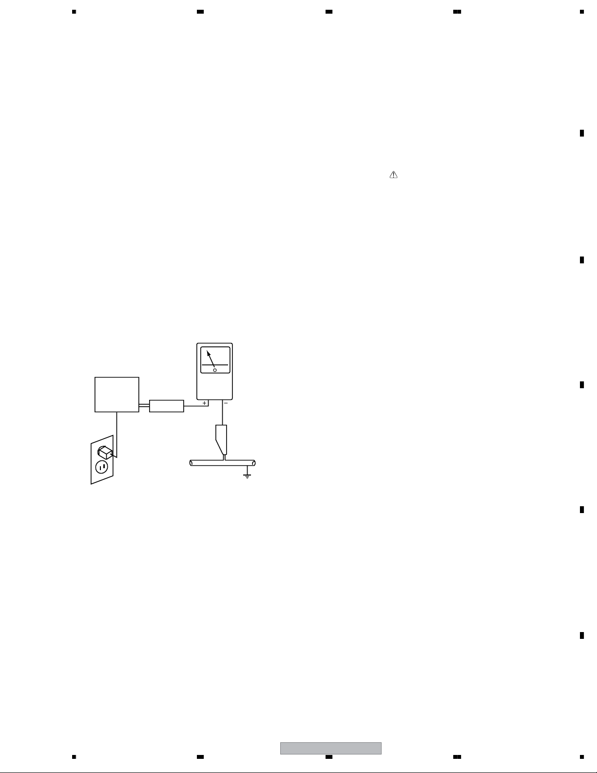
Leakage Current Cold Check
With the AC plug removed from an AC power source, place a
jumper across the two plug prongs. Turn the AC power switch on.
Using an insulation tester (DC 500V), connect one lead to the
jumpered AC plug and touch the other lead to each exposed metal
part (input/output terminals, screwheads, metal overlays, control
shafts, etc.), particularly any exposed metal part having a return
path to the chassis. Exposed metal parts having a return path to
the chassis should have a minimum resistor reading of 0.3MΩ
and a maximum resistor reading of 5MΩ. Any resistor value
below or above this range indicates an abnormality which requires
corrective action. Exposed metal parts not having a return path to
the chassis will indicate an open circuit.
Leakage Current Hot Check
Plug the AC line cord directly into an AC power source (do not
use an isolation transformer for this check).
Turn the AC power switch on.
Using a "Leakage Current Tester (Simpson Model 229
equivalent)", measure for current from all exposed metal parts of
the cabinet (input/output terminals, screwheads, metal overlays,
control shaft, etc.), particularly any exposed metal part having a
return path to the chassis, to a known earth ground (water pipe,
conduit, etc.). Any current measured must not exceed 0.5mA.
PRODUCT SAFETY NOTICE
Many electrical and mechanical parts in PIONEER set have
special safety related characteristics. These are often not evident
from visual inspection nor the protection afforded by them
necessarily can be obtained by using replacement components
rated for higher voltage, wattage, etc. Replacement parts which
have these special safety characteristics are identified in this
Service Manual.
Electrical components having such features are identified by
marking with a on the schematics and on the parts list in this
Service Manual.
The use of a substitute replacement component which dose not
have the same safety characteristics as the PIONEER
recommended replacement one, shown in the parts list in this
Service Manual, may create shock, fire or other hazards.
Product Safety is continuously under review and new instructions
are issued from time to time. For the latest information, always
consult the current PIONEER Service Manual. A subscription to,
or additional copies of, PIONEER Service Manual may be
obtained at a nominal charge from PIONEER.
A
B
C
Reading should
not be above
0.5mA
Earth
ground
Device
under
test
Also test with
plug reversed
(Using AC adapter
plug as required)
Leakage
current
tester
Test all
exposed metal
surfaces
AC Leakage Test
ANY MEASUREMENTS NOT WITHIN THE LIMITS
OUTLINED ABOVE ARE INDICATIVE OF A POTENTIAL
SHOCK HAZARD AND MUST BE CORRECTED BEFORE
RETURNING THE SET TO THE CUSTOMER.
D
E
56
PDP-425CMX
F
3
7
8
1234
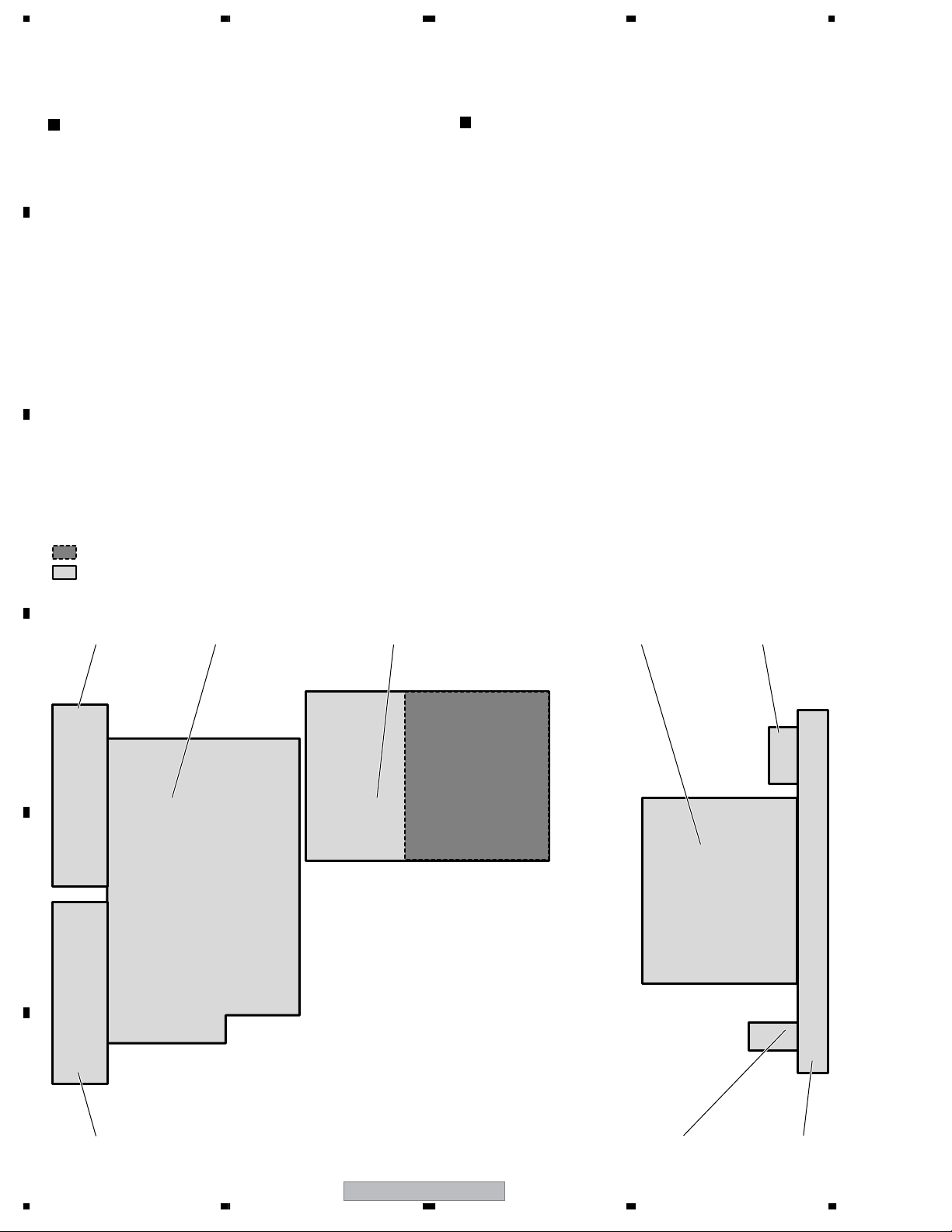
A
Charged Section
The places where the commercial AC power is used without
passing through the power supply transformer.
If the places are touched, there is a risk of electric shock. In
addition, the measuring equipment can be damaged if it is
connected to the GND of the charged section and the GND of the
non-charged section while connecting the set directly to the
commercial AC power supply. Therefore, be sure to connect the
set via an insulated transformer and supply the current.
B
1. Power Cord
2. AC Inlet
3. Power Switch (S1)
4. Fuse (In the POWER SUPPLY Unit)
5. STB Transformer and Converter Transformer
(In the POWER SUPPLY Unit)
6. Other primary side of the POWER SUPPLY Unit
C
: Part is Charged Section.
: Part is the High Voltage Generating Points
other than the Charged Section.
High Voltage Generating Point
The places where voltage is 100V or more except for the charged
places described above. If the places are touched, there is a risk of
electric shock.
If the procedures described in “7.1.4 POWER ON/OFF
FUNCTION FOR THE LARGE POWER SIGNAL SYSTEM”
are performed before the power is turned off, the voltage will be
discharged in about 30 seconds.
1. POWER SUPPLY Unit.....................................................(205V)
2. 42 X DRIVE Assy .......................................... (–180V to 205V)
3. 42 Y DRIVE Assy .......................................................... (500V)
4. 42 SCAN A Assy ............................................................ (500V)
5. 42 SCAN B Assy ............................................................(500V)
6. SUS CLAMP 1 Assy .......................................(–180V to 205V)
7. SUS CLAMP 2 Assy .......................................(–180V to 205V)
42 SCAN B Assy
D
E
42 Y DRIVE Assy 42 X DRIVE Assy SUS CLAMP 1 AssyPOWER SUPPLY Unit
F
42 SCAN A Assy SUS CLAMP 2 Assy PLATE X (FT)
Fig.1 Charged Section and High Voltage Generating Point (Rear View)
4
1234
PDP-425CMX
5678
[Important Check Points for Good Servicing]
In this manual, procedures that must be performed during repairs are marked with the below symbol.
Please be sure to confirm and follow these procedures.
1. Product safety
Please conform to product regulations (such as safety and radiation regulations), and maintain a safe servicing environment by
following the safety instructions described in this manual.
1 Use specified parts for repair.
Use genuine parts. Be sure to use important parts for safety.
2 Do not perform modifications without proper instructions.
Please follow the specified safety methods when modification(addition/change of parts) is required due to interferences such as
radio/TV interference and foreign noise.
3 Make sure the soldering of repaired locations is properly performed.
When you solder while repairing, please be sure that there are no cold solder and other debris.
Soldering should be finished with the proper quantity. (Refer to the example)
4 Make sure the screws are tightly fastened.
Please be sure that all screws are fastened, and that there are no loose screws.
5 Make sure each connectors are correctly inserted.
Please be sure that all connectors are inserted, and that there are no imperfect insertion.
6 Make sure the wiring cables are set to their original state.
Please replace the wiring and cables to the original state after repairs.
In addition, be sure that there are no pinched wires, etc.
7 Make sure screws and soldering scraps do not remain inside the product.
Please check that neither solder debris nor screws remain inside the product.
8 There should be no semi-broken wires, scratches, melting, etc. on the coating of the power cord.
Damaged power cords may lead to fire accidents, so please be sure that there are no damages.
If you find a damaged power cord, please exchange it with a suitable one.
9 There should be no spark traces or similar marks on the power plug.
When spark traces or similar marks are found on the power supply plug, please check the connection and advise on secure
connections and suitable usage. Please exchange the power cord if necessary.
0 Safe environment should be secured during servicing.
When you perform repairs, please pay attention to static electricity, furniture, household articles, etc. in order to prevent injuries.
Please pay attention to your surroundings and repair safely.
A
B
C
D
2. Adjustments
To keep the original performance of the products, optimum adjustments and confirmation of characteristics within specification.
Adjustments should be performed in accordance with the procedures/instructions described in this manual.
3. Lubricants, Glues, and Replacement parts
Use grease and adhesives that are equal to the specified substance.
Make sure the proper amount is applied.
4. Cleaning
For parts that require cleaning, such as optical pickups, tape deck heads, lenses and mirrors used in projection monitors, proper
cleaning should be performed to restore their performances.
5. Shipping mode and Shipping screws
To protect products from damages or failures during transit, the shipping mode should be set or the shipping screws should be
installed before shipment. Please be sure to follow this method especially if it is specified in this manual.
56
PDP-425CMX
E
F
5
7
8

1234
CONTENTS
1. SPECIFICATIONS ............................................................................................................................................ 7
2. EXPLODED VIEWS AND PARTS LIST .......................................................................................................... 10
A
B
C
D
2.1 PACKING SECTION ................................................................................................................................10
2.2 FRONT and REAR SECTION.................................................................................................................. 12
2.3 TERMINAL SECTION .............................................................................................................................. 14
2.4 MULTIBASE SECTION ............................................................................................................................ 16
2.5 FRAME SECTION.................................................................................................................................... 18
2.6 DRIVE SECTION ..................................................................................................................................... 20
2.7 CHASSIS SECTION ................................................................................................................................22
3. BLOCK DIAGRAM AND SCHEMATIC DIAGRAM..........................................................................................24
3.1 OVERALL CONNECTION DIAGRAM (1/2) ............................................................................................. 24
3.2 OVERALL CONNECTION DIAGRAM (2/2) ............................................................................................. 26
3.3 OVERALL BLOCK DIAGRAM (1/2) ......................................................................................................... 28
3.4 OVERALL BLOCK DIAGRAM (2/2) ......................................................................................................... 30
3.5 MAIN ASSY BLOCK DIAGRAM............................................................................................................... 32
3.6 COMMON SLOT ASSY ...........................................................................................................................34
3.7 KEY, LED, SENB, SENC and SEND ASSYS........................................................................................... 35
3.8 AUDIO and SUS COMM IF ASSYS......................................................................................................... 36
3.9 POWER BLOCK DIAGRAM..................................................................................................................... 38
3.10 CONNECTOR PIN DESCRIPTION .......................................................................................................40
5. PCB PARTS LIST ........................................................................................................................................... 56
6. ADJUSTMENT ............................................................................................................................................... 69
6.1 ADJUSTMENT REQUIRED WHEN THE SET IS REPAIRED OR REPLACED....................................... 69
6.2 ADJUSTMENT......................................................................................................................................... 70
6.3 SERVICE MENU LIST ............................................................................................................................. 73
6.4 SERVICE MENU...................................................................................................................................... 74
6.5 FACTORY MODE..................................................................................................................................... 76
6.6 RS-232C C0MMAND ............................................................................................................................... 87
6.7 METHOD FOR REPLACING THE SERVICE PANEL ASSY.................................................................. 115
7. GENERAL INFORMATION........................................................................................................................... 121
7.1 DIAGNOSIS ........................................................................................................................................... 121
7.1.1 PCB LOCATION ..............................................................................................................................121
7.1.2 DIAGNOSIS OF SHUTDOWN/POWER-DOWN INDICATED BY LEDS.......................................... 122
7.1.3 TROUBLESHOOTING..................................................................................................................... 128
7.1.4 POWER ON/OFF FUNCTION FOR THE LARGE POWER SIGNAL SYSTEM............................... 157
7.1.5 BACKUP WHEN THE MAIN UNIT IS ADJUSTED ..........................................................................158
7.1.6 HOW TO CLEAR HISTORY DATA ................................................................................................... 160
7.1.7 FAN CONTROL ...............................................................................................................................162
7.1.8 POWER ON SEQUENCE................................................................................................................ 163
7.1.9 DISASSEMBLY................................................................................................................................ 164
7.2 IC ........................................................................................................................................................... 170
8. PANEL FACILITIES ...................................................................................................................................... 180
E
F
6
1234
PDP-425CMX

5678
1. SPECIFICATIONS
General
Light emission panel ................ 42V type AC Plasma Panel
92.16 cm (W) x 51.53 cm (H) x 105.59 cm (diagonal)
Number of pixels .............................................. 1024 x 768
Power supply (for 425CMX)....... AC 100 - 120 V, 50/60 Hz
(for 42MXE10)...... AC 100 - 240 V, 50/60 Hz
Rated current (for 425CMX)........................... 3.0 A - 2.5 A
(for 42MXE10)......................... 3.0 A - 1.3 A
Standby power consumption (for 425CMX).............. 1.2 W
(for 42MXE10)............ 1.5 W
External dimensions
............................... 1022 mm (W) x 610 mm (H) x 98 mm
(D: Not including handles)
40-1/4 in. (W) x 24 in. (H) x 3-7/8 in.
(D: Not including handles)
(including display stand)
....................... 1218 mm (W) x 737 mm (H) x 300 mm (D)
47-31/32 in. (W) x 29-1/32 in. (H) x 11-13/16 in. (D)
Weight .......................................................30.5 kg (67 lbs.)
(including display stand)............................31.1 kg (69 lbs.)
Input/output
Video
INPUT1
Input Mini D-sub 15 pin (socket connector)
RGB signal (G ON SYNC compatible)
RGB ... 0.7 Vp-p/75 Ω/no sync.
HD/VS, VD ... TTL level
/positive and negative polarity
/2.2 kΩ
G ON SYNC
... 1 Vp-p/75 /negative sync.
*Compatible with Microsoft “ Plug & Play”
(VESA DDC1/2B)
Output Mini D-sub 15 pin (socket connector)
75Ω /with buffer
INPUT2
Input DVI-D 24-pin connector
Digital RGB signal (DVI compliant TMDS
signal)
*Compatible with Microsoft “ Plug & Play”
(VESA DDC 2B)
Audio
Input AUDIO INPUT (for INPUT1)
Stereo mini jack
L/R ... 500 mVrms/more than 10 kΩ
AUDIO INPUT (for INPUT2)
Stereo mini jack
L/R ... 500 mVrms/more than 10 kΩ
Output AUDIO OUTPUT
Stereo mini jack
L/R ... 500 mVrms (max)/less than 5 kΩ
SPEAKER
L/R ... 6 Ω/8 W +8 W (at 6Ω )
Control
RS-232C... D-sub 9 pin (pin connector)
COMBINATION IN/OUT
... Mini DIN 6 pin (x2)
Accessories
Power cord (for 425CMX)..................................................1
Remote control unit ......................................................... 1
Remote control unit holder .............................................. 1
AA (R6) batteries.............................................................. 2
Cleaning cloth (for screen) ............................................... 1
Speed clamps................................................................... 5
Display stands .................................................................. 2
Washers ........................................................................... 2
Hex hole bolts (M8X40).................................................... 2
Ferrite cores (for power cord) .......................................... 2
Ferrite cores (for audio cables)......................................... 3
Cable ties ......................................................................... 2
Operating Instructions (for 425CMX)................................ 1
Operating Instructions (CD-ROM) (for 42MXE10).............1
Start up Guide (for 42MXE10) ......................................... 1
Warranty(for 425CMX)..................................................... 1
A
B
C
D
¶ Due to improvements, specifications and design are subject to
change without notice.
PDP-425CMX
56
E
F
7
7
8

1234
A
1 Power cord
(ADG1215)
2 Remote control unit
(AXD1528)
7 Ferrite cores (x 3) (for audio cables)
(CTX1054)
B
3 AA (R6) batteries (x 2)
C
4 Cleaning cloth (for screen)
(AED1285)
5 Speed clamps (x 5)
(AEC2051)
D
8 Display stands (x 2)
(AMR3545)
9 Washers (x 2)
(WB80FTC)
0 Hex hole bolts (x 2)
(SMZ80H400FTC)
- Remote control unit holder
(AMR3268)
6 Ferrite cores (x 2) (for power cord)
(ATX1031)
E
F
8
1234
Use as a holder for the
remote control unit.
When attaching to the
rear of the main unit,
be careful not to cover
the vents.
= Cable ties (x 2)
(AEC-093)
• These Operating Instructions
• Warranty
PDP-425CMX

5678
A
B
C
D
E
56
PDP-425CMX
F
9
7
8

1234
2. EXPLODED VIEWS AND PARTS LIST
NOTES:
Parts marked by "NSP" are generally unavailable because they are not in our Master Spare Parts List.
The mark found on some component parts indicates the importance of the safety factor of the part.
A
Therefore, when replacing, be sure to use parts of identical designation.
Screws adjacent to mark on product are used for disassembly.
For the applying amount of lubricants or glue, follow the instructions in this manual.
(In the case of no amount instructions, apply as you think it appropriate.)
2.1 PACKING SECTION
B
12
14×2
13×2
C
6×5
5×2
24
10×2
11
PDP-425CMX
23
only
22
25
×3
9
×2
35
33
7, 15-17, 19,
20, 37-39
D
21
4
E
8
2, 3
PDP-425CMX
only
29
1
32
31
30
36
18
(Except
PDP-42MXE10/YVXK5)
27
28
26
F
34
10
1234
PDP-425CMX
>
5678
(1) PACKING SECTION PARTS LIST
No. Description Part No.
Mark
1Power Cord See Contrast table (2)
2 Remote Control Unit
3 Battery Cover
NSP 4 Dry Cell Battery (R6P, AA) VEM1031
5 Cable tie AEC-093
AXD1528
AZN2462
No. Description Part No.
Mark
19 Caution Sheet ARM1245
20 Caution Sheet See Contrast table (2)
NSP 21 Warranty Card See Contrast table (2)
NSP 22 Warranty Card See Contrast table (2)
NSP 23 Polyethylene Bag See Contrast table (2)
A
6 Speed clamp AEC2051
7 Cleaning Cloth AED1285
8 Remote Control Holder AMR3268
9 Display Stand AMR3545
10 Ferrite Core (for power cord) ATX1031
11 Ferrite Core (for audio cables) CTX1054
12 Screws Set AXX1071
13 Hex hole bolt SMZ80H400FTC
14 Washer WB80FTC
15 Operating Instructions See Contrast table (2)
(English, French, Japanese)
16 Operating Instructions See Contrast table (2)
(English)
17 Operating Instructions See Contrast table (2)
(7L)(CD-ROM)
18 Caution Sheet See Contrast table (2)
24 Catalogue Bag AHG1310
25 Catalogue Bag S AHG1338
26 Pad BL (FT) See Contrast table (2)
27 Pad BR (FT) See Contrast table (2)
28 Pad BC (FT) See Contrast table (2)
29 Pad TL (FT) See Contrast table (2)
30 Pad TR (FT) See Contrast table (2)
31 Accessory Case See Contrast table (2)
32 Power Cord Case See Contrast table (2)
33 Reinforce Pad (FT) See Contrast table (2)
34 Carton (42FT) See Contrast table (2)
35 Upper Carton See Contrast table (2)
36 Mirror Mat See Contrast table (2)
37 Plasma Caution Sheet See Contrast table (2)
38 Image Caution Sheet See Contrast table (2)
39 Image Stick Caution Sheet See Contrast table (2)
(2) CONTRAST TABLE
PDP-425CMX/LUC5, PDP-42MXE10/LDFK5 and YVXK5 are constructed the same except for the following:
Mark No. Symbol and Description
>
1Power Cord ADG1215 Not used Not used
15 Operating Instructions (English, French, Japanese) ARD1070 Not used Not used
16 Operating Instructions (English) Not used ARE1419 ARE1419
17 Operating Instructions (7L)(CD-ROM) Not used ARU1001 ARU1001
18 Caution Sheet ARM1201 ARM1201 Not used
PDP-425CMX
/LUC5
PDP-42MXE10
/LDFK5
PDP-42MXE10
/YVXK5
B
C
D
20 Caution Sheet Not used Not used ARM1279
NSP 21 Warranty Card ARY1146 Not used Not used
NSP 21 Warranty Card (EU) Not used ARY1149 ARY1149
NSP 22 Warranty Card ARY1146 Not used Not used
NSP 23 Polyethylene Bag AHG-195 Not used Not used
26 Pad BL (FT) AHA2495 AHA2495 AHA2528
27 Pad BR (FT) AHA2496 AHA2496 AHA2529
28 Pad BC (FT) AHA2497 AHA2497 AHA2530
29 Pad TL (FT) AHA2522 AHA2522 AHA2531
30 Pad TR (FT) AHA2523 AHA2523 AHA2532
31 Accessory Case AHC1072 AHC1072 AHC1078
32 Power Cord Case AHC1077 AHC1077 AHC1081
33 Reinforce Pad AHC1079 AHC1079 AHC1080
34 Carton (42FT) AHD3417 AHD3417 AHD3458
35 Upper Carton AHD3418 AHD3455 AHD3461
36 Mirror Mat AHG1284 AHG1284 AHG1327
37 Plasma Caution Sheet ARM1147 Not used Not used
38 Image Caution Sheet ARM1220 Not used Not used
39 Image Stick Caution Sheet ARM1299 Not used Not used
PDP-425CMX
56
7
8
E
F
11

1234
2.2 FRONT and REAR SECTION
A
314
33
3
B
C
D
7
21
5
11
PDP-425CMX
only
22
3
3
1613
1
12
22 22 22 22
21
15
21 21
3
22
3
3
3 3
224 2
5
6
22
18
22
22
E
8
22
22
F
12
1234
22
22
22
9 10
22
22
22
22 1922
22
22
22
22
22
PDP-425CMX
22
22
22
22
22
22
22
22
17

>
5678
(1) FRONT and REAR SECTIONS PARTS LIST
No. Description Part No.
Mark
1 KEY Assy AWW1108
2 LED2 Assy AWW1109
NSP 3 Panel Holder (FT) ANG2840
4 PCB Spacer AEC1947
5 Inner Grip Assy AMR3434
NSP 6 Name Label See Contrast table (2)
7 Serial Sheet AAX3143
8Terminal Label MAIN A (CMX) See Contrast table (2)
9Terminal Label MAIN B (CMX) See Contrast table (2)
10 Terminal Label MAIN C (CMX) See Contrast table (2)
A
11 Caution Label (CMX) See Contrast table (2)
12 Caution Label See Contrast table (2)
13 Front Case Assy (425CMX) AMB2885
14 Filter (FT) AMR3510
15 Control Button (CMX) AAC1559
16 Pioneer Badge AAM1101
17 Control Cover (CMX) AMR3512
18 Rear Case ANE1650
19 Bottom Cover (CMX) ANG2860
20 • • • • •
21 Screw ABZ30P100FTB
22 Screw AMZ30P060FTB
(2) CONTRAST TABLE
PDP-425CMX/LUC5, PDP-42MXE10/LDFK5 and YVXK5 are constructed the same except for the following:
Mark No. Symbol and Description
NSP 6 Name Label (CMX) AAL2726 Not used Not used
NSP 6 Name Label (MXE) Not used AAL2734 AAL2746
8Terminal Label MAIN A (CMX) AAX3250 AAX3250 AAX3292
9Terminal Label MAIN B (CMX) AAX3251 AAX3251 AAX3293
10 Terminal Label MAIN C (CMX) AAX3252 AAX3252 AAX3294
PDP-425CMX
/LUC5
PDP-42MXE10
/LDFK5
PDP-42MXE10
/YVXK5
B
C
D
11 Caution Label (CMX) AAX3253 Not used Not used
12 Caution Label M AAX3304 AAX3304 Not used
12 Caution Label Not used Not used AAX3295
PDP-425CMX
56
7
8
E
F
13
1234
2.3 TERMINAL SECTION
A
Filter styling
28
27
5, 28
43
31
5
32
29
36
32
45
4
45
44
8
16
5, 28
5, 28
11
28
5, 28
18
4040
43
14
43
5, 28
383838
3737
91
3423
43
17
43
43
B
12
5, 28
C
313
42
D
35
43
43
33
24
43
29
26
42
43
29
2
33
43
29
43
5, 28
28
32
39
10
43
30
E
F
19
15
30
4321 43
5, 28
43
25
14
1234
30
43
PDP-425CMX
20
43 43
42 42
38
41 41
227 6
43

5678
TERMINAL SECTION PARTS LIST
No. Description Part No.
Mark
1AUDIO Assy AWW1105
2 COMMSLOT Assy AWW1106
3 COMMSLOT IF Assy AWW1107
4 SENC Assy AWW1103
5 Filter CTX1054
6Power Switch (S1) ASG1094
7AC Inlet (CN1) AKP1296
8 1P Wire GND (J209) ADX3242
9 9P Housing Wire (J220) ADX3262
10 7P Housing Wire (J201) ADX3263
>
>
A
11 13P Housing Wire (J202) ADX3264
12 8P Housing Wire (J204) ADX3265
13 40P Housing Wire (J205) ADX3268
14 6P Housing Wire (J222) ADX3270
15 8P Housing Wire (J221) ADX3283
16 Housing Wire (J216) ADX3284
17 Housing Wire (J210) ADX3285
18 13P Housing Wire (J218) ADX3286
19 COMM Bracket (CMX) ANG2857
20 Terminal Panel AC (CMX) ANG2863
21 Terminal Panel COMM (CMX) ANG2874
22 AC Bracket (CMX) Assy ANG2901
NSP 23 Audio Heatsink ANH1648
24 Slot Spring T94 ABK1034
25 Slot Spring B92 ABK1035
26 COMM I/F Bracket (CMX) ANG2859
27 Inlet Cover (XM4) ANG2899
28 Nyron Binder AEC-093
29 Wire Saddle AEC1745
30 Mini Clamp AEC1805
31 Harness Lifter 18 AEC1980
32 Omega Lock AEC2084
33 COMM Rail (CMX) AMR3486
34 Thermal Sheet AUDIO AMR3507
35 Gasket ANK1823
B
C
D
36 Gasket ANK1827
37 Gasket ANK1828
38 Gasket ANK1829
39 Gasket ANK1830
40 Gasket ANK1831
41 Screw ABA1342
42 Screw ABZ30P100FTB
43 Screw AMZ30P060FTB
44 Screw BMP40P080FBN
45 PCB Spacer AEC1941
56
PDP-425CMX
E
F
15
7
8

1234
2.4 MULTIBASE SECTION
A
19
19
19
7
3
21
17
23
23
16
23
5
21
3
3
21
9
2 12
24 24
18
13
14141414
4
21
13
13
13
24
6
23
13
17
23
23
21
15
B
1414
C
D
21
14
1
21
21
21 21
22 22
E
F
22
16
1234
222222
PDP-425CMX
11
10
8

5678
(1) MULTI BASE SECTION PARTS LIST
No. Description Part No.
Mark
1 MAIN Assy See Contrast table (2)
2 VSIF Assy See Contrast table (2)
3 Flexible Cable (J219) ADD1342
4 20P Housing Wire (J215) ADX3273
5 20P Housing Wire (J217) ADX3274
A
6LVDS Cable (J223)
7 Multi Base (CMX) ANA1901
8
11 Slot Panel 262 (N) ANG2610
12 VIDEO I/F Bracket ANG2858
13 Wire Saddle AEC1745
14 Wire Saddle AEC1797
15 PCB Support AEC1958
16 Rivet AMR1066
17 VIDEO Guide Rail AMR3485
18 VIDEO I/F Sheet AMR3495
19 PWB Sleeve AMR3518
20 • • • • •
21 Screw AMZ30P060FTB
22 Hex Head Screw BBA1051
23 Screw PMB30P100FNI
24 Screw VBB30P080FNI
Te r minal Panel MAIN (CMX) Assy
9 Slot Spring T130 ABK1032
10 Slot Spring B126 ABK1033
ADX3276 (or ADX3289)
ANG2871
B
C
(2) CONTRAST TABLE
PDP-425CMX/LUC5, PDP-42MXE10/LDFK5 and YVXK5 are constructed the same except for the following:
Mark No. Symbol and Description
1 MAIN Assy AWW1100 AWW1112 AWW1112
2 VSIF Assy AWW1101 AWW1113 AWW1113
PDP-425CMX
/LUC5
PDP-42MXE10
/LDFK5
PDP-42MXE10
/YVXK5
D
E
F
56
PDP-425CMX
17
7
8

1234
2.5 FRAME SECTION
A
20
3
B
31 31
C
31
31
15
30
20
17 24
31
29
31
30
26
13
17
22
21
14
20
17
23
29
7
31
31
31
30
26
31
31
31
22
21
20
1
8
15
30
17
17
D
28
E
31
17
31
17
29 29
28
31
12
31
17
18
5, 16
31
18
19
19
19
19
17
28
17
19
6
31
19
28
19
31
F
28
10 11
18
1234
282828
3131
PDP-425CMX
31
25
9
25
31

5678
FRAME SECTION PARTS LIST
No. Description Part No.
Mark
1 SENB Assy AWW1102
2• • • • •
3 SEND Assy AWW1104
4• • • • •
5 Filter CTX1054
6 3P Housing Wire (J206) ADX3266
7 4P Housing Wire (J207) ADX3267
8Front Chassis U (FT) ANA1907
9Front Chassis R (FT) ANA1918
10 Front Chassis LA ANA1926
A
11 Front Chassis LB (FT) ANA1928
12 Front Chassis B (CMX) ANA1933
13 Sub Frame L Assy (CMX) ANG2875
14 Sub Frame R Assy (CMX) ANG2876
15 Fan Angle (FT) ANG2909
16 Nyron Binder AEC-093
17 Wire Saddle AEC1745
18 Wire Saddle AEC1751
19 Mini Clamp AEC1805
20 PCB Spacer AEC1941
21 Cushion A AED1293
22 Cushion B AED1294
23 Duct Sheet L (FT) AMR3515
24 Duct Sheet R (FT) AMR3532
25 Gasket ANK1823
26 Fan Motor 80 x 25L AXM1054
27 • • • • •
28 Screw AMZ30P060FTB
29 Screw PMB50P120FTC
30 Screw PPZ50P100FTB
31 Screw VBB30P080FNI
B
C
D
56
PDP-425CMX
E
F
19
7
8

1234
2.6 DRIVE SECTION
A
9
222222
23
B
C
7
23
14 4
23
23
13
22
23
23
23
1920
6, 16
1018 18
D
E
F
22
18
18
18
12
23
2
18
23
11
181818
23
18
18
23
5
3
23
23
222222222222
23
8
1
22
20
PDP-425CMX
1234

5678
DRIVE SECTION PARTS LIST
No. Description Part No.
Mark
1 SUS CLAMP 1 Assy AWW1022
2 SUS CLAMP 2 Assy AWW1023
3 42 X DRIVE Assy AWW1067
4 42 Y DRIVE Assy AWV2251
5POWER SUPPLY Unit AXY1127
6Ferrite Core ATX1039
7 4P Housing Wire (J101) ADX3192
8 6P Housing Wire (J102) ADX3193
9 3P Housing Wire (J103) ADX3194
10 8P Housing Wire (J105) ADX3196
>
A
11 14P Housing Wire (J106) ADX3292
12 5P Housing Wire (J108) ADX3199
13 9P Housing Wire (J104) ADX3278
14 6P Housing Wire (J107) ADX3280
15 • • • • •
16 Nyron Binder AEC-093
17 • • • • •
18 Locking Wire Saddle AEC1992
19 HS Sheet S (FT) AMR3519
20 HS Sheet L (FT) AMR3520
21 • • • • •
22 Screw PMB30P060FTC
23 Screw VBB30P080FNI
B
C
D
56
PDP-425CMX
E
F
21
7
8

1234
2.7 CHASSIS SECTION
A
Note : The parts of encircled number denote measuring component of PDP Service Assy.
18
15
16
20
16
19
20
20
16
16
16
16
15
14
10
16
9
14
14
B
17 8
C
14
14
11
16
16
16
16
141414
13
13
16
7
5
16
14
13
16
17
16
16
13
13
16
12
D
6666
1
16
E
3
2
F
4 4 4 4
16
1616
16
22
PDP-425CMX
1234

5678
(1) PANEL CHASSIS SECTION PARTS LIST
No. Description Part No.
Mark
NSP 1 Panel Chassis (FT) Assy See Contrast table (2)
2 42 SCAN A Assy AWW1071
3 42 SCAN B Assy AWW1072
4 42 ADDRESS Assy AWV2253
5 MD DIGITAL Assy AWV2254
No. Description Part No.
Mark
11 Flexible Cable (J120) ADD1333
12 Flexible Cable (J211) ADD1334
13 Wire Saddle AEC1745
14 Flat Clamp AEC1879
15 PCB Support AEC1938
A
6Ferrite Core ATX1048
7 Flexible Cable (J109) ADD1329
8 Flexible Cable (J110) ADD1330
9 Flexible Cable (J117) ADD1331
10 Flexible Cable (J119) ADD1332
16 PCB Spacer AEC1941
17 Drive Silicone Sheet AEH1095
18 Power Sheet (FT) AMR3521
19 Y Drive Protect Sheet (FT) AMR3525
20 Harness Lifter 18 AEC1980
(2) CONTRAST TABLE
PDP-425CMX/LUC5, PDP-42MXE10/LDFK5 and YVXK5 are constructed the same except for the following:
Mark No. Symbol and Description
NSP 1 Panel Chassis (FT) Assy AWU1136 AWU1136 AWU1151
PDP-425CMX
/LUC5
PDP-42MXE10
/LDFK5
PDP-42MXE10
/YVXK5
2.8 PDP SERVICE ASSY
PDP SERVICE ASSY PARTS LIST
No. Description Part No.
No. Description Part No.
Mark
PDP Service Assy 42H6D1 AWU1160
NSP Panel Chassis (FT) Assy AWU1136
Wire Saddle AEC1745 x5
Flat Clamp AEC1879 x9
PCB Support AEC1938 x2
PCB Spacer AEC1941 x22
Harness Lifter 18 AEC1980 x2
Power Sheet (FT) AMR3521
Y Drive Protect Sheet (FT) AMR3525
Caution Label AAX3031 x2
Screw PMB50P150FTC x4
Mark
Accessories
Wire Saddle AEC1745 x13
PCB Spacer AEC1941 x4
Harness Lifter 18 AEC1980
Locking Wire Saddle AEC1992 x11
Vinyl Bag S AHG1338
Sheet (FT) AMR3530 x2
Packing parts
Pad 42 Single (T-L) AHA2550
Pad 42 Single (T-R) AHA2551
Pad 42 Single (B-L) AHA2552
Pad 42 Single (B-R) AHA2553
Upper Carton (42 Single) AHD3480
B
C
D
E
Under Carton (42 Single) AHD3481
Polyethylene Bag AHG1381
Packing Sheet AHG1386
Tr ay (FT) AHX1158
Cup Spacer (15) ANG2936 x4
PDP-425CMX
56
F
23
7
8

1234
3. BLOCK DIAGRAM AND SCHEMATIC DIAGRAM
3.1 OVERALL CONNECTION DIAGRAM (1/2)
A
÷
When ordering service parts, be sure to refer to "EXPLODED VIEWS and PARTS
LIST" or "PCB PARTS LIST".
÷
The > mark found on some component parts indicates the importance of the safety
factor of the part. Therefore, when replacing, be sure to use parts of identical
designation.
ADX3268
123
1
FAN-CTL
2
GND
3
F-ALM
FB
FAN-CTL
1
GND
103
103
2
3
1
2
3
4
5
6
7
8
1
2
3
4
5
6
7
8
9
...
...
F-ALM
A+12
A.GND
A+6
A+6
A.GND
A.GND
NC
NC
AU-L
GND
AU-R
GND
SP_ALM
GND
MUTE
SCL7
SDA7
CN2303
AKP1252
.
.
123
124
232425
123
124
232425
FA
CN9008
AKM1279
CN9001
AKM1280
125
125
CN4004→CN5301
26.→25.GPC4
27.→24.GPC2
28.→23.GPC5
29.→22.GND
30.→21.VYOBI1
31.→10.VYOBI2
32.→19.GND
33.→18.DSUBSW_DET
34.→17.G4G
35.→16.FNC0
36.→15.IR
37.→14.SLOT_ST2
38.→13.FNC1
39.→12.S_DIN_SEL
40.→11.SLOT_ST1
41.→10.IN4_DET
42. →9.GND
43. →8.SDA_VS
44. →7.SCL_VS
45. →6.SDA5
46. →5.SCL5
47. →4.GND
48. →3.VCC_DOWN1
49. →2.PNP_WR
50. →1.NC
CN9004
AKM1274
CN9003
AKM1274
PV
AU
CN5010
AKM1343
246..
135..
.
363840
.
353739
CN9010
AKM1342
CN5001, CN4005
1.GND
3.Y(G)ON_SYNC
5.GND
7.B(B-Y)
9.GND
11.R(R-Y)
13.GND
15.HD_SA
17.GND
19.VD_SA
151719
.
161820
.
ADX3274
151719
.
161820
.
CN4005 AKM1343
CN4003→CN6302
1.→50.GA4
2.→49.GND
3.→48.GB4
4.→47.GND
5.→46.GA3
6.→45.GND
7.→44.GB5
8.→43.GND
9.→42.GA2
10.→41.GND
11.→40.GB6
12.→39.GND
13.→38.GA1
14.→37.GND
15.→39.GB7
16.→35.GND
17.→34.GA0
18.→33.GND
19.→32.BB0
20.→31.GND
21.→30.RA7
22.→29.GND
23.→28.BB1
24.→27.GND
25.→26.RA6
SCL5
TM
2.NC
4.GND
6.MC
8.GND
10.NC
12.GND
14.AUDIO_R
16.GND
18.AUDIO_L
20.GND
135..
246..
135..
246..
CN4006
AKP1251
26.→25.GND
27.→24.BB2
28.→23.GND
29.→22.RA5
30.→21.GND
31.→10.BB3
32.→19.GND
33.→18.RA4
34.→17.GND
35.→16.BB4
36.→15.GND
37.→14.RA3
38.→13.GND
39.→12.BB5
40.→11.GND
41.→10.RA2
42.→ 9.GND
43. →8.BB6
44. →7.GND
45. →6.RA1
46. →5.GND
47. →4.BB7
48. →3.GND
49. →2.RA0
50. →1.GND
4
1234567
GND
VDD+3.3V
CN9501
AKM1275
SDA5
M+7V
PM
D.GND
NCNCNCNCNC
CN9006
AKM1278
MAIN ASSY
PDP-425CMX
AWW1100
CN5301 AKM1345 CN6302 AKM1345
123..
CN4004 AKM1345 CN4003 AKM1345 CN4002 AKM1345
196
CN4002→CN6301
1.→50.VD
2.→49.HD
3.→48.DE
4.→47.CLK
5.→46.GND
6.→45.RB0
7.→44.GND
8.→43.BA7
9.→42.GND
10.→41.RB1
11.→40.GND
12.→39.BA6
13.→38.GND
14.→37.RB2
15.→39.GND
16.→35.BA5
17.→34.GND
18.→33.RB3
19.→32.GND
20.→31.BA4
21.→30.GND
22.→29.RB4
23.→28.GND
24.→27.BA3
25.→26.GND
.
484950
ADD1342 ADD1342- ADD1342
195
484950
194
949596
.
...
...
CN4006
Card edge
connector
26.→25.RB5
27.→24.GND
28.→23.BA2
29.→22.GND
30.→21.RB6
31.→10.GND
32.→19.BA1
33.→18.GND
34.→17.RB7
35.→16.GND
36.→15.BA0
37.→14.GND
38.→13.GB0
39.→12.GND
40.→11.GB1
41.→10.GND
42.→ 9.GB1
43.→ 8.GND
44.→ 7.GA6
45.→ 6.GND
46.→ 5.GB2.
47. 4.GND
48.→ 3.GA5
49.→ 2.GND
50.→ 1.GB3
167
166
123..
165
656667
1.GND
3.G
5.B
7.R
9.HD_SA
11.VD_SA
13.AUDIO_L
15.AUDIO_R
17.SLOT_ST1
19.FNC1
21.V+3.3V
23.NC
25.HD_DET
27.VD
29.HD
31.GND
33.RB1
35.RB3
37.RB5
39.RB7
41.GND
43.GB1
45.GB3
47.GB5
49.GB7
53.GND
55.BB1
57.BB3
59.BB5
61.BB7
65.GND
67.KEY
69.TXD_CARD
71.INT_EXT
73.EMGREQ1_V
75.IC1V_OE
77.NC
79.FNC2
81.SOUND1
83.DSUBR
85.DSUBG
87.SDUBB
89.IN5_HD
91.GPC1
93.GPC5
95.VYOBI2
12345
D+3.3
D+3.3
PN1 PN2
PDP-42MXE10
AWW1112
123..
.
484950
.
154
160
161
162
...
606162
...
2.GND
4.GND
6.GND
8.GND
10.GND
12.GND
14.GND
16.GND
18.S_DIN_SEL
20.FNC0
22.V+3.3V
24.GND
26.GND
28.GND
30.GND
32.RB0
34.RB2
36.RB4
38.RB6
40.GND
42.GB0
44.GB2
46.GB4
48.GB6
52.GND
54.BB0
56.BB2
58.BB4
60.BB6
62.GND
66.GND
68.NC
70.RXD_CARD
72.NC
74.EMGREQ2_V
76.RESETX1
78.SD_SEL
80.FNC3
82.GND
84.GND
86.GND
88.GND
90.SOUSA_X
92.GPC2
94.VYOBI1
96.DSUNSW_DET
FAN(1&2)
AXM1054
"FAN" may be connected
B
to either "FA" or "FB"
CN9010,CN2302
1.VCC_DOWN2
3.NC
5.NC
7.LEDCTL1
C
D
9.LEDCTL2
11.RLS
13.VDDM3.3V
15.VDDM5V
17.4G/5G
19.TXD2
21.PLE_CTL2
23.RXD2
25.PLE_CTL
27.STL_LINK
29.CB_MUTE
31.KEY
33.RXD
35.TXD
37.GND
39.GPC1
CN2301
KM200NA8L
LEDCTL1LEDCTL1
REMIN
1234567
1234567
REMIN
LEDCTL2 LEDCTL2
LED2 ASSY
AWW1109
E
CN2303,Card edge connector
1.NC
2.IRSW
3.IR_COMM_OUT
4.IR_COMM_IN
5.GND
6.GND
7.GND
8.CYOBI3
9.CYOBI2
10.CSL_ST2
11.CSL_ST1
14.GND
15.GND
16.FIRST_RXD
17.GET_UART
18.INT_EXT
19.RXD_CARD
20.TXD_CARD
21.GPC5
F
22.GPC4
23.GPC3
24.GPC2
25.GPC1
FAN(1) FAN(2)
2.V+6.5V
4.CSL_ST1
6.REMIN
8.GND
10.CYOBI3
12.CYOBI2
14.CSL_ST2
16.VDDM3.3V
18.GND
20.VDDM5V
22.GND
24.FIRST_RXD
26.GET_UART
28.INT_EXT
30.RXD_GU
32.TXD_GU
34.GPC5
36.GPC4
38.GPC3
40.GPC2
CN2302
AKM1347
246..
135..
COMM SLOT I/F ASSY
AWW1107
VDDM5V
VDDM3.3V
GND
RLS
GND
8
ADX3283
8
GND
RLS
GND
VDDM5V
CN2101
VDDM3.3V
AKM1294
COMM SLOT
ASSY
AWW1106
101.NC
102.GND
103.GND
104.GND
105.TXD_PDP
106.RXD_PDP
107.KEY_COMM_IN
108.CB_MUTE
109.STL_LINK
110.GND
111.GND
114.V+6.5V
115.V+6.5V
116.GND
117.GND
118.VDDM3.3V
119.VDDM3.3V
120.VDDM5
121.APL_CTL1
122.APL_RXD
123.APL_CTL2
124.APL_TXD
125.SLT_Vrer
ADX3262
AU:SHIELD-WIRE
(1,3pin:shield)
.
363840
.
353739
101
102
123..
101
102
123..
Card edge connector
1.←50.VDDM3.3V
2.→49.NC
3.→48.NC
4.→47.KEY
5.→46.GND
6.→45.GET_UART
7.→44.TXD_CARD
8.→43.FIRST_RXD
9.→42.RXD_CARD
10.→41.INT_EXT
11.→40.GND
12.→39.RESETX1
13.→38.SLOT_ST3
14.→37.SD_SEL
15.→39.SOUND2
16.→35.FNC3
17.→34.FNC2
18.→33.SOUND1
19.→32.GND
20.→31.IN5_VD
21.→30.IN5_HD
22.→29.GND
23.→28.HYOUJI_X
24.→27.GPC3
25.→26.GPC1
D+3.3
D.GND
D.GND
CN9007
AKM1277
484950
123..
152
153
525354
6
1234567
D+2.7
D+2.7
D.GND
CN6301 AKM1345
123..
484950
147
148
149
474849
.
101.GND
103.GND
105.GND
107.GND
109.GND
111.GND
113.GND
115.V+13.5
117.IN4_DET
119.SLOT_ST2
121.NC
123.GND
125.3G4G
127.GND
129.GND
131.GND
133.BA6
135.BA4
137.BA2
139.BA0
141.GND
143.GA6
145.GA4
147.GA2
149.GA0
153.GND
155.RA6
157.RA4
159.RA2
161.RA0
165.GND
167.VSEPSCL
169.NC
171.FIRST_RXD
173.EMGREQ1_S
175.IC1S_OE
177.NC
179.SLOT_ST3
181.SOUND2
183.GND
185.GND
187.GND
189.IN5_VD
191.GPC3
193.NC
195.VYOBI5
NC
D+2.7
D.GND
D.GND
CN9012
AKM1278
CN8502 AD2
1.GND
3.P_ST_B
5.NC
7.NC
9.NC
11.NC
13.NC
15.NC
17.NC
19.GND
.
484950
.
101
102
103
...
123..
D.GND
2.GND
4.MR_ST_B
6.MR_RXD
8.AC_DET_B
10.REQ
12.MR_TXD
14.STB_MUTE
16.VIS
18.FIELD
20.GND
123..
102.GND
104.SCL_VS
106.SDA_VS
108.GND
110.V+12V
112.V+12V
114.V+3.3STB
116.V+13.5
118.IN3_DET
120.IR
122.NC
124.GND
126.IN5_DET
128.DE
130.CLK
132.BA7
134.BA5
136.BA3
138.BA1
140.GND
142.GA7
144.GA5
146.GA3
148.GA1
152.GND
154.RA7
156.RA5
158.RA3
160.RA1
162.GND
166.GND
168.VSEPSDA
170.GET_UART
172.NC
174.EMGREQ2_S
176.NC
178.NC
180.M_CHOICE
182.GND
184.DSUBH
186.DSUBV
188.GND
190.HYOUJI_X
192.GPC4
194.VYOBI4
196.VYOBI6
24
PDP-425CMX
1234

5678
SW
CN9011
AKM1274
AD2
CN8502
AKM1343
CN8501 AD1
1.GND
2.GND
3.GND
4.RE+
5.RE-
6.RD+
7.RD-
8.RCLK+
9.RCLK-
10.GND
11.RC+
12.RC-
13.RB+
14.RB-
15.RA+
VIDEO SLOT IF ASSY
PDP-425CMX
AWW1101
16.RA-
17.GND
18.NC
19.NC
20.NC
21.NC
22.NC
23.NC
24.GND
25.MSEL
26.POWER
27.
STB_MUTE
28.RFU
29.STATUS
30.GND
31.GND
123456789
CN4001 AKM1299
PDP-42MXE10
VDDM3
KEY
GND
1
3
5
.
.
.
15
17
19
AD1
CN8501
AKM1339
101112
AWW1113
TEMP-SENSOR1
SENB ASSY
CN1001
AKM1279
TM2
SCL5
GND
VDD+3.3V
SDA5
SCL5
GND
VDD+3.3V
123
4
ADX3267
1
2
3
2
4
6
.
.
.
16
18
20
1
2
3
.
.
.
29
30
31
13
ADX3263
ADX3264
1.+16.5V
2.NC
ADX3265
ADX3286
PM
PN
3.GND
PV
PA
ADX3270
M+7V
7
D.GND
6
NC
5
NC
4
NC
3
NC
2
NC
1
12
D+3.3
11
D+3.3
10
D+3.3
9
D.GND
8
D.GND
7
D.GND
6
D+2.7
5
D+2.7
4
D+2.7
3
D.GND
2
D.GND
1
D.GND
A+12
8
A.GND
7
A+6
6
A+6
5
A.GND
4
A.GND
3
NC
2
NC
1
6
S+12
5
S+12
4
S+12
3
GND
2
GND
1
GND
SDA5
567
8
ADX3271
ADX3276 (or ADX3289)
POWER SUPPLY
AXY1127
GND_SUS
GND_SUS
PS
13
A+12V
12
A+12V
11
A.GND
10
A.GND
9
NC
8
NC
7
D+3.3
6
D+3.3
5
D.GND
4
D.GND
3
STB3.3
2
D.GND
1
NC
GND_ADR
GND_ADR
+16.5V
+6.5V
GND_D
VSUS
VSUS
+60V
+60V
NC
NC
P2
P6
1
2
3
4
56
7
8
1
2
3
4
5
GND_SUS
GND_SUS
GND_D
GND_D
STB3.3V
GND_STB
STB_MUTE_B
EXT_PD
VSUS_ADJ
AC_DET
PD_TRG_B
GND_ADR
GND_ADR
P3
CN4001
1.A+12V
2.A+12V
3.A.GND
4.A.GND
5.A+16.5V
6.A.GND
7.D+3.3
8.D+3.3
9.D,GND
10.D.GND
11.STB3.3
12.D.GND
13.NC
123456789
AU-L
S+12
1
S+12
2
S+12
3
GND
4
GND
5
GND
6
AUDIO ASSY
GND
AU-R
PA
CN3003
AKM1277
GND
GND
SP_ALM
MUTE
SCL7
SDA7
AU
CN3004
AKM1280
AC INLET
+16.5V
+6.5V
GND_D
VSUS
VSUS
+8V
+8V
PS_PD
RELAY
DRF_B
+60V
+60V
L
1
AKP1296
NC
NC
NC
NC
TEMP-SENSOR3
SEND ASSY
AWW1104AWW1102
SCL5
GND
VDD+3.3V
1234567
P1
1
2
3
ADX3278
4
56
7
8
9
ADX3196
P4
1
2
3
4
5
6
7
8
9
ADX3292
1011
1213
14
ADX3199
1
P7
2
3
4
ADX3198
5
6
N
2
ADX3284
ADX3285
TM3
SDA5
CN1201
AKM1279
SCL5
GND
VDD+3.3V
SDA5
8
TEMP-SENSOR2
SENC ASSY
AWW1103
CN1101
AKM1275
TM4
PDP Md
AWV2251
Y4(CN2350)
AWV2250
X2(CN1201)
AWV2254
D2(CN3002)
D1(CN3001)
D11(CN3601)
AWV2253
(3/4)
AD2(CN1502)
AWV2253
(4/4)
AD2(CN1502)
AWV2253
(2/4)
AD2(CN1502)
AWV2251
Y4(CN2350)
SCL5
GND
123
AC Switch
ASG1094
VDD+3.3V
SDA5
4
A
B
C
D
E
AWW1105
ROUT+
ROUT-
LOUT+
LOUT-
123
4
SPEAKER_OUT
PDP-425CMX
56
AC
SW
KEY ASSY
AWW1108
F
25
8
1
VDDM3V
2
KEY
CN2201
3
ADX3266
GND
S3B-EH
7

1234
3.2 OVERALL CONNECTION DIAGRAM (2/2)
A
B
C
Overall Wiring Diagram (2/2)
D
E
F
26
PDP-425CMX
1234

5678
A
B
C
D
E
56
PDP-425CMX
F
27
7
8
1234
3.3 OVERALL BLOCK DIAGRAM (1/2)
A
B
C
D
E
General Block Diagram (1/2)
KEY ASSY
S2201
S2202
S2203
S2204
S2205
S2206
S2207
S2208
IC2201
X2201
3.84MHz
(DIN)
MAIN ASSY
CN7001
INPUT2
(DVI)
CN5002
INPUT1
(15p D-SUB)
CN5003
ANALOG
RGB OUT
(15p D-SUB)
CN5001
CN4005
AV
+7V
IC7006
7V to 5V
RGB
H/V
RGB
H/V
IC5001
BUF
CN6301
CN4002
IC7001
DVI
Receiver
+3.3V
IC5002
+5V
IC5004
Video SW
+9V
IC5007
BUF
+5V
IC5008
BUF
+3.3V
H/V
D1
VIDEO SLOT I/F ASSY
CN4006
VIDEO SLOT
CN2201
IC7003
5V to 3.3V
H/V
+3.3V
IC5005
SyncSW
IC6301
OE
CN6302
CN4003
D2
COMM SLOT ASSY
CN2001
(9p D-SUB)
JA2002
(DIN)
JA2003
(DIN)
H/V
CN5301
CN4004
D3
IC2003
232C
Transceiver
+5V
IC5601
Video
SW
IC5603
Sync SW
IC5901
Video
SW
IC5902
Sync SW
CN4001
PS
+3.3V
+5V
+3.3V
RGB
H/V
RGB
H/V
L/R
IC2001
IC2002
IC2004
IC2005
IC2006
IC2007
LPF
LPF
INPUT1
JA5371
INPUT2
JA5372
OUTPUT
JA5373
(mini Jack)
L/R
(mini Jack)
L/R
(mini Jack)
L/R
COMM SLOT I/F ASSY
CN2303
CN2004
IC5602
+5V
IC5605
Sync sep
+5V
IC5905
LPF
IC5903
Sync sep
RGB
+5V
LPF
H/V
+5V
H/V
H/V
IC5308
RGB
IC5606
+12V
Audio
SW
IC2301
SEL
+5V
BUF
IC5904
CN9011
IC5604
SW
H/V
+3.3V
SW
IC8002
2.5V to 1.5V
IC8003
3.3V to 1.5V
X8001
X8002
CN2301
CN2302
SW
KEY
H/V
H/V
+2.5V
+3.3V
CLK
CLK
F
28
Control signal
Analog Video signal
Sync signal
Power Supply
PDP-425CMX
Digital Video signal, CLK, Sync
TMDS, LVDS
Digital Audio signal
Analog Audio signal
1234
5678
A
LED2 ASSY
CN2401
U2401
Remote Control Receiver
D2402
LED
SENB ASSY
IC1001
+3.3V
SEND ASSY
IC1201
+3.3V
SENC ASSY
IC1101
+3.3V
D2401
CN1001
Opt Sense
CN9010 CN9501
TXD/RXD
IC9501
u-COM
7V to 3.3V
+7V
IC9502
7V to 5V
+3.3V
IC8105
OSD
+3.3V
IC8501
LVDS
Transmitter
IC8101~8104
SDRAM
IC9503
LVDS
+3.3V
+7V
SCL,
SDA
L/R
+3.3V
RGB/
CLK
Converter
+3.3V
IC9504
BUF
+3.3V
IC6701
A/D
Converter
H/V
IC5306
Audio Buffer
IC6501
A/D
H/V
+3.3V
RGB/
CLK
X9501
33.333MHz
+3.3V
IC8001
Digital signal
Processor
RGB/
CLK/H/
V/DE
+12V
TM
D9003,4
Alarm
detect
TXD,
RXD
+12V
+6V
+7V
+3.3V
+2.5V
CN8502
AD2
CN8501
AD1
CN9001
AU
CN1201
CN9008
PV
FA
CN9004 CN9005 CN9003
FB
CN9006
PM
CN9007
PN1
CN9012
PN2
CN3003
#2, 27
CN3004
#11, 19
DC detect
AUDIO ASSY
CN1101
FAN
IC3004
12V to 9V
IC3001
Audio
Controller
+12V
IC3002
Audio
Amplifier
(1)
FAN
(2)
FAN
(3)
+9V
+9V
+12V
#31, 32
#36, 38
#41, 43
#47, 48
B
C
A
To Power Supply (2/2)
B
C
D
D
F
E
To Md (2/2)
H
G
E
SP OUT
CN3001
F
56
PDP-425CMX
29
7
8

1234
3.4 OVERALL BLOCK DIAGRAM (2/2)
General Block Diagram (2/2)
A
PDP Module
Scan Signal
VH
B
C
To MAIN (1/2)
IC2801
IC5V
Scan IC
PSUS
IC2802
Scan IC
IC2803
Scan IC
IC2804
Scan IC
IC2805
Scan IC
IC2806
Scan IC
CN2802
Serial Data
CN2702
IC2701
Scan IC
IC2702
Scan IC
IC2703
Scan IC
IC2704
Scan IC
IC2705
Scan IC
D1
G
H
D2
IC2706
Scan IC
PSUS
IC5V
VH
Scan Signal
SCAN B ASSY (UPPER)
VH
SB1
Y2
PSUS
PSUS
Y3
SA1
IC5V
VH
IC5V
Photo Coupler
VH VSUS
VH DC/DC Conv.
Vprst
Vprst Reg.
+5V +16.5V
VSUS
IC2252
Mask
Mod.
+5V
SUSOUT
VSUS
+5V
+16.5V
IC2253
Mask
Mod.
+16.5V
Soft-D
Block
IC5V
IC5V
Block
IC5V/VF
DC/DC
VF
Conv.
Vprst
+ Reset
Block
VOFS
Regulator
+16.5V
Resonance
Block
+5V
+16.5V
IC2101
DK Mod.
+16.5V
Scan Signal
VSUS
+6.5V
+5V
VOFS
DC/DC
Conv.
Y4
+5V
Logic
Block
Offset
Block
VOFS
+16.5V
Drive Signal
Y1
+5V
Y5
60V
Y6
P6 P1
V+8V
Block
V+ADR5
CLK/LE/HBLK/LBLK
IC1555
Driver IC
CN1501
AN/P BN/P
CN/P DN/P CLKN/P
R/G/B
Driver IC
IC1554
(PEE002A-K)
V+3V
LVDS Receiver
IC1501
AD1 AD2
D
Resonance
IC1553
Driver IC
CN1502
V+60VV+5V
Resonance
V+ADR1
IC1552
Driver IC
Block
AD1 AD2
Resonance
V+8V
Block
V+ADR5
CLK/LE/HBLK/LBLK
IC1555
Driver IC
CN1501
AN/P BN/P
CN/P DN/P CLKN/P
R/G/B
Driver IC
IC1554
(PEE002A-K)
V+3V
IC1501
LVDS Receiver
IC1553
Driver IC
CN1502
V+60VV+5V
Resonance
V+ADR1
IC1552
Driver IC
Block
P6 P1
Power Supply Unit AXY1127-
PV
E
A
To MAIN (1/2)
B
C
D
PM
PN
PA
+12V
+6V
+7V
+3.3V
+2.7V
+12V
E
F
PS
F
+3.3V
+12V
+3.3STB
P3
+16.5V
+6.5V
Vsus
+16.5V
+6.5V
Vsus
+8V
+STB3.3V
STB_MUTE_B
EXT_PD
VSUS_ADJ
PS_PD
RELAY
DRF_B
AC_DET
PD_TRIG_B
+60V
+60V
P1
P2
P4
P6
P7
+16.5V
30
PDP-425CMX
1234
 Loading...