

Page 1

PIONEER CORPORATION 4-1, Meguro 1-chome, Meguro-ku, Tokyo 153-8654, Japan
PIONEER ELECTRONICS (USA) INC. P.O. Box 1760, Long Beach, CA 90801-1760, U.S.A.
PIONEER EUROPE NV Haven 1087, Keetberglaan 1, 9120 Melsele, Belgium
PIONEER ELECTRONICS ASIACENTRE PTE. LTD. 253 Alexandra Road, #04-01, Singapore 159936
PIONEER CORPORATION 2005
ORDER NO.
ARP3302
PDP-42A3HD
PLASMA DISPLAY
PDP-42A3HD
PDP-4214HD
< CAUTION >
This ARP3302 Supersedes ARP3270
THIS MANU
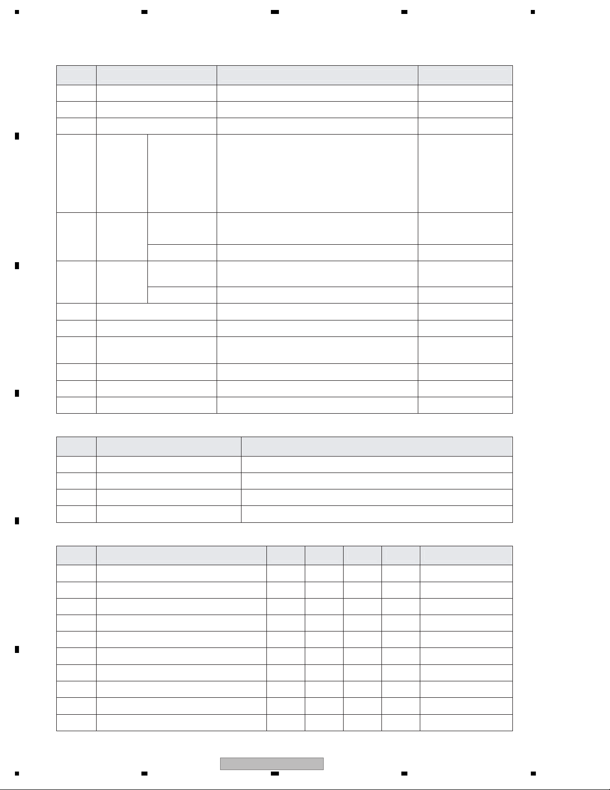
Model Type Power Requirement Remarks
PDP-42A3HD KUCXKA AC120V
PDP-42A3HD KUCXC AC120V
PDP-4214HD KUCXC AC120V
AL IS APPLICABLE TO THE FOLLOWING MODEL(S) AND TYPE(S).
For details, refer to "Important symbols for good services".
T-ZZR OCT. 2005 printed in Japan
Page 2

1234
SAFETY INFORMATION
A
This service manual is intended for qualified service technicians ; it is not meant for the casual doit-yourselfer. Qualified technicians have the necessary test equipment and tools, and have been
trained to properly and safely repair complex products such as those covered by this manual.
Improperly performed repairs can adversely affect the safety and reliability of the product and may
void the warranty. If you are not qualified to perform the repair of this product properly and safely,
you should not risk trying to do so and refer the repair to a qualified service technician.
WARNING
This product contains lead in solder and certain electrical parts contain chemicals which are known to the state of California to
cause cancer, birth defects or other reproductive harm.
B
NOTICE
(FOR CANADIAN MODEL ONLY)
Fuse symbols (fast operating fuse) and/or (slow operating fuse) on PCB indicate that replacement parts
must be of identical designation.
REMARQUE
(POUR MODÈLE CANADIEN SEULEMENT)
Les symboles de fusible (fusible de type rapide) et/ou (fusible de type lent) sur CCI indiquent que les pièces
de remplacement doivent avoir la même désignation.
Health & Safety Code Section 25249.6 - Proposition 65
C
SAFETY PRECAUTIONS
NOTICE : Comply with all cautions and safety related notes
located on or inside the cabinet and on the chassis.
The following precautions should be observed :
1. When service is required, even though the PDP UNIT an
isolation transformer should be inserted between the power line
and the set in safety before any service is performed.
2. When replacing a chassis in the set, all the protective devices
D
must be put back in place, such as barriers, nonmetallic knobs,
adjustment and compartment covershields, isolation resistorcapacitor, etc.
3. When service is required, observe the original lead dress. Extra
precaution should be taken to assure correct lead dress in the
high voltage circuitry area.
4. Always use the manufacture's replacement components.
Especially critical components as indicated on the circuit
diagram should not be replaced by other manufacture's.
Furthermore where a short circuit has occurred, replace those
components that indicate evidence of overheating.
E
5. Before returning a serviced set to the customer, the service
technician must thoroughly test the unit to be certain that it is
completely safe to operate without danger of electrical shock,
and be sure that no protective device built into the set by the
manufacture has become defective, or inadvertently defeated
during servicing. Therefore, the following checks should be
performed for the continued protection of the customer and
servicetechnician.
6. Perform the following precautions against unwanted radiation
and rise in internal temperature.
• Always return the internal wiring to the original styling.
• Attach parts (Gascket, Ferrite Core, Ground, Rear Cover,
Shield Case etc.) surely after disassembly.
7. Perform the following precautions for the PDP panel.
• When the front case is removed, make sure nothing hits the
panel face, panel corner, and panel edge (so that the glass does
not break).
• Make sure that the panel vent does not break. (Check that the
cover is attached.)
• Handle the FPC connected to the panel carefully.
Twisting or pulling the FPC when connecting it to the
connector will cause it to peel off from the panel.
8. Pay attention to the following.
• When the front case is removed, infrared ray is radiated and
may disturb reception of the remote control unit.
• Pay extreme caution when the front case and rear panel are
removed because this may cause a high risk of disturbance to
TVs and radios in the surrounding.
F
2
1234
PDP-42A3HD
Page 3

5678
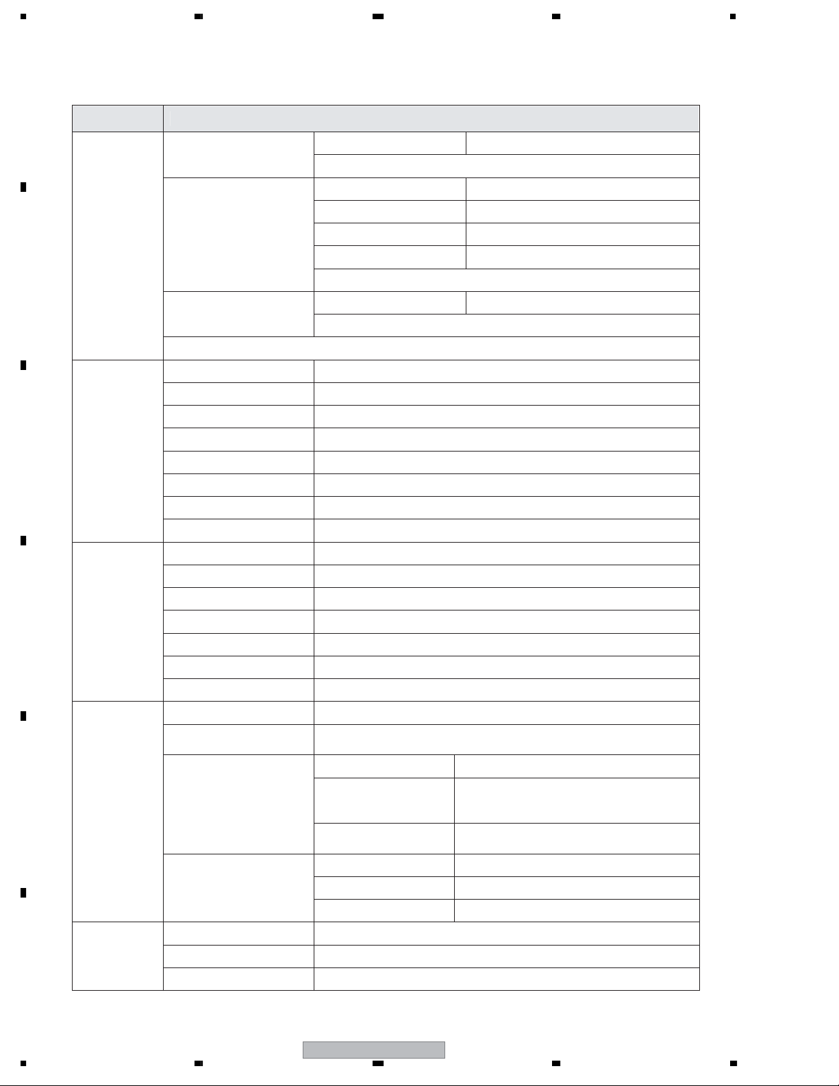
Leakage Current Cold Check
With the AC plug removed from an AC power source, place a
jumper across the two plug prongs. Turn the AC power switch on.
Using an insulation tester (DC 500V), connect one lead to the
jumpered AC plug and touch the other lead to each exposed metal
part (input/output terminals, screwheads, metal overlays, control
shafts, etc.), particularly any exposed metal part having a return
path to the chassis. Exposed metal parts having a return path to
the chassis should have a minimum resistor reading of 0.3MΩ
and a maximum resistor reading of 5MΩ. Any resistor value
below or above this range indicates an abnormality which requires
corrective action. Exposed metal parts not having a return path to
the chassis will indicate an open circuit.
Leakage Current Hot Check
Plug the AC line cord directly into an AC power source (do not
use an isolation transformer for this check).
Turn the AC power switch on.
Using a "Leakage Current Tester (Simpson Model 229
equivalent)", measure for current from all exposed metal parts of
the cabinet (input/output terminals, screwheads, metal overlays,
control shaft, etc.), particularly any exposed metal part having a
return path to the chassis, to a known earth ground (water pipe,
conduit, etc.). Any current measured must not exceed 0.5mA.
PRODUCT SAFETY NOTICE
Many electrical and mechanical parts in PIONEER set have
special safety related characteristics. These are often not evident
from visual inspection nor the protection afforded by them
necessarily can be obtained by using replacement components
rated for higher voltage, wattage, etc. Replacement parts which
have these special safety characteristics are identified in this
Service Manual.
Electrical components having such features are identified by
marking with a on the schematics and on the parts list in this
Service Manual.
The use of a substitute replacement component which dose not
have the same safety characteristics as the PIONEER
recommended replacement one, shown in the parts list in this
Service Manual, may create shock, fire or other hazards.
Product Safety is continuously under review and new instructions
are issued from time to time. For the latest information, always
consult the current PIONEER Service Manual. A subscription to,
or additional copies of, PIONEER Service Manual may be
obtained at a nominal charge from PIONEER.
A
B
C
Reading should
not be above
0.5mA
Earth
ground
Device
under
test
Also test with
plug reversed
(Using AC adapter
plug as required)
Leakage
current
tester
Test all
exposed metal
surfaces
AC Leakage Test
ANY MEASUREMENTS NOT WITHIN THE LIMITS
OUTLINED ABOVE ARE INDICATIVE OF A POTENTIAL
SHOCK HAZARD AND MUST BE CORRECTED BEFORE
RETURNING THE SET TO THE CUSTOMER.
D
E
56
PDP-42A3HD
F
3
7
8
Page 4

1234
A
CAUTION
• Observe the caution matter, without fail
• The caution matters of given in the delivery specifications, etc., must be observed, without fail.
• Do not give shocks and vibration.
• The panel surface (display plane) of the PDP module is made of glass. If any shocks or vibration is applied, it may be broken and
the scattered glass chips will be a cause of injury
• Do not put anything.
B
• Transportation must be done by enough personnel.
• Do
not put anything on the PDP module. Otherwise, this can be a cause of injury as a result of falling down or dropping caused
by imbalance.
• The PDP module is heavy. In the case of transportation, unpacking, or packing, more than two persons should do it by supporting
the top and the bottom of the product.
7 Miscellaneous caution matters
(1) This PDP module uses highly integrated semiconductor parts. Since these parts are fragile to electrostatic
charges, earth bands should be used for handling. The product should be handled where measures have been
taken against electrostatic charges.
(2) For this product, the PDP modules and the PWBs are repaired by replacement in a unit. Therefore, the units of
C
the PWBs must not be repaired or disassembled. Otherwise, the validity of warranty will be lost.
(3) If this PDP module is used for the fixed character display or the like as in the case of a character display board,
a phenomenon of burning (not warranted) will occur. Burning is a phenomenon that the unevenness in the
brightness is caused in the display. In such a case, the brightness in the section where the integrated display
time is longer becomes lower than the brightness in another section where the integrated display time is shorter.
This phenomenon is in proportion to the integrated display time and the brightness. For this reason, to relieve
this difficulty during servicing, do not use any still picture, but use a display by motion pictures of a video or the
like. In addition, use “FULL” for the screen mode and avoid using any display by “NORMAL”, “TRUE”, or MULTI
SCREEN like side by side etc. If it is necessary to use only a still picture for unavoidable reasons, use a burning
relief function such as “PLE LOCK”, “ORBITER”, “SCREEN WIPER”, etc.
(4) When a PDP module is operated after a long time of storage, it may encounter a difficulty like a failure in
displaying a screen or unstability according to the condition of storage. In such a case, the PDP module should
D
be incorporated in the product and aging treatment should be carried out for about two hours (all screen display).
(5) Sulfides will deteriorate the PDP module and this is a cause of malfunction. Therefore, it is absolutely prohibited
to put any vulcanized rubber or a material containing sulfur in the vicinity of the PDP module.
(6) When taking out a PDP module from the maintenance package box, do it slowly so that the panel surface
does not get any shock or stress.
(7) If one touches the connector of the flexible cable exposed to the rear side of the PDP module, there is
danger of causing a poor contact. As such, it must be handled with utmost care. In addition, the flexible cable
is very weak in mechanical strength. Therefore, this cable must not be touched during handling.
(8) The panel surface of the PDP module is easy to be hurt and generate cracks. Therefore, it should be handled
very carefully. Never press or rub it with a hard thing. Never put it on a hard thing with the panel surface faced
downwards.
(9) When the panel surface of the PDP module is contaminated, gently wipe off the contaminant with a piece of
E
soft dry cloth. Liquid-state contamination can be removed by lightly pressing it, without rubbing it. If it is
difficult to remove the contamination, use a piece of cloth soaked with a neutral detergent. The cloth for
wiping off should be clean. Never use the same cloth repeatedly. If a cleansing detergent or water drops
should enter the module interior or be attached to the module surface other than the display plane at the time
of cleaning, this will give rise to the destruction of the product when the product is energized.
(10) When transporting this PDP module, use the packing materials specified in the list of parts. Once used,
such packing materials should not be used again.
(11) The PDP module is composed of a variety of parts, such as those made of materials like glass, metal,
plastics, etc. Therefore, when abandoning the PDP module, this should be done in accordance with the
relevant law of the nation or an autonomous body
F
4
1234
PDP-42A3HD
Page 5
5678
SAFETY SERVICE
7 Safety cautions
The matters to be observed without fail are explained below. These matters are indispensable for the preventi on of an
accident during the maintenance servicing, the [security of products] after the completi on of servicing work, and the
[prevention of the repeated occurrence of similar fault.]
(1) The degree of danger and material damage, caused as a result of wrong use by disregarding the contents of the display”
is distinguished and explained in the table below.
WARNING
CAUTION
(2) Kinds of the matters to be observed are classified and explained in the icons shown below.
This icon indicates a dangerous place where an electric shock is anticipated.
This icon indicates the contents of “caution” that must be borne in mind, without fail.
If this display is disregarded and equipment is handled wrongly, this can be a cause of physical injury and
a fire, thus leading a person to death or serious injury.
If this display is disregarded and equipment is handled wrongly, this may lead to personal injury or
material damage.
A
B
This icon indicates the contents of “caution” that must be practiced, without fail.
WARNING
• Observe the caution matter, without fail.
• In the place where a particular caution is needed during maintenance servicing, such a caution note is displayed with a label or a
stamp that is given to the cabinet, chassis, PWB, etc. These caution notes and also the caution matters of given
in the instruction manuals, etc., must be observed, without fail.
• Be careful of an electric shock or a burn.
• The PDP module involves the sections where high voltage and high temperature are prevalent. When equipment is energized,
therefore, use working gloves in order to prevent an electric shock and a burn. At the time of transportation, disassembly,
reassembly, and the replacement of parts, such a servicing job must be done after pulling out all the connector cables that have
been connected with external equipment.
• Modification of equipment is absolutely prohibited. Use the specified parts at all times.
• If any modification is performed, the validity of the manufacturer’s warranty is lost at that moment. The personnel who did this
modification is responsible for the physical injury or the like, if it should occur as a result of the modification. The parts used are
given the safety-based characteristics, such as non-flammability or sufficient
CAUTION
• Danger of explosion if battery is incorrectly replaced.
• Replace only with the same or equivalent type.
WARNING
C
D
E
56
PDP-42A3HD
F
5
7
8
Page 6
1234
[Important Check Points for Good Servicing]
In this manual, procedures that must be performed during repairs are marked with the below symbol.
Please be sure to confirm and follow these procedures.
A
1. Product safety
Please conform to product regulations (such as safety and radiation regulations), and maintain a safe servicing environment by
following the safety instructions described in this manual.
1 Use specified parts for repair.
Use genuine parts. Be sure to use important parts for safety.
2 Do not perform modifications without proper instructions.
Please follow the specified safety methods when modification(addition/change of parts) is required due to interferences such as
radio/TV interference and foreign noise.
B
C
D
3 Make sure the soldering of repaired locations is properly performed.
When you solder while repairing, please be sure that there are no cold solder and other debris.
Soldering should be finished with the proper quantity. (Refer to the example)
4 Make sure the screws are tightly fastened.
Please be sure that all screws are fastened, and that there are no loose screws.
5 Make sure each connectors are correctly inserted.
Please be sure that all connectors are inserted, and that there are no imperfect insertion.
6 Make sure the wiring cables are set to their original state.
Please replace the wiring and cables to the original state after repairs.
In addition, be sure that there are no pinched wires, etc.
7 Make sure screws and soldering scraps do not remain inside the product.
Please check that neither solder debris nor screws remain inside the product.
8 There should be no semi-broken wires, scratches, melting, etc. on the coating of the power cord.
Damaged power cords may lead to fire accidents, so please be sure that there are no damages.
If you find a damaged power cord, please exchange it with a suitable one.
9 There should be no spark traces or similar marks on the power plug.
When spark traces or similar marks are found on the power supply plug, please check the connection and advise on secure
connections and suitable usage. Please exchange the power cord if necessary.
0 Safe environment should be secured during servicing.
When you perform repairs, please pay attention to static electricity, furniture, household articles, etc. in order to prevent injuries.
Please pay attention to your surroundings and repair safely.
2. Adjustments
To keep the original performance of the products, optimum adjustments and confirmation of characteristics within specification.
Adjustments should be performed in accordance with the procedures/instructions described in this manual.
3. Lubricants, Glues, and Replacement parts
Use grease and adhesives that are equal to the specified substance.
E
Make sure the proper amount is applied.
4. Cleaning
For parts that require cleaning, such as optical pickups, tape deck heads, lenses and mirrors used in projection monitors, proper
cleaning should be performed to restore their performances.
5. Shipping mode and Shipping screws
To protect products from damages or failures during transit, the shipping mode should be set or the shipping screws should be
installed before shipment. Please be sure to follow this method especially if it is specified in this manual.
F
6
1234
PDP-42A3HD
Page 7

5678
CONTENTS
SAFETY INFORMATION......................................................................................................................................2
1. SPECIFICATIONS
2. EXPLODED VIEWS AND PARTS LIST...........................................................................................................14
2.1 PACKING
2.2 EXTERIOR SECTION (1)
2.3 EXTERIOR SECTION (2)
2.4 FRONT PANEL SECTION ........................................................................................................................20
2.5 REAR SECTION.......................................................................................................................................21
3. BLOCK DIAGRAM AND SCHEMATIC DIAGRAM ..........................................................................................22
3.1 BLOCK DIAGRAM....................................................................................................................................22
3.1.1 OVERALL BLOCK DIAGRAM
3.1.2 ATSC BLOCK
3.1.3 DISPLAY BLOCK
3.2 DIGITAL B/D SCHEMATIC DIAGRAM......................................................................................................30
3.3 DTT_ANALOG B/D...................................................................................................................................36
4. PCB DIAGRAM ...............................................................................................................................................44
4.1 DIGITAL B/D .............................................................................................................................................44
4.2 DTT_ANALOG B/D...................................................................................................................................46
4.3 CONTRPL IR & LED, SUB_AV&, SUB_KEY, EMI and POWER B/D ................................................48
5. PCB PARTS LIST............................................................................................................................................50
6. ADJUSTMENT ................................................................................................................................................53
6.1 ADJUSTMENT OF WHITE BALANCE
6.2 OPERATION TEST IN EACH MODE
6.3 TV .............................................................................................................................................................55
6.4 SPEAKER & INTERFACE
7. GENERAL INFORMATION .............................................................................................................................58
7.1 DIAGNOSIS..............................................................................................................................................58
7.1.1 OPERATION SEQUENCE FLOW
7.1.2 TROUBLE SHOOTING METHOD
7.1.3 DTT BASIC INSPECTION
7.1.4 BASIC INSPECTION
7.1.5 CPU / SYSTEM MEMORY INSPECTION
7.1.6 MPEG INSPECTION..........................................................................................................................96
7.1.7 A/ V INSPECTION..............................................................................................................................97
7.1.8 CHANNEL INSPECTION .................................................................................................................100
7.1.9 CHANNEL INSPECTION 2 ..............................................................................................................102
7.1.10 DISASSEMBLY ..............................................................................................................................104
7.2 HOW TO DIAGNOSE THE PDP MODULE.............................................................................................108
8. PANEL FACILITIES
14
16
18
22
23
26
53
54
56
58
60
88
89
94
135
8
A
B
C
D
56
PDP-42A3HD
E
F
7
7
8
Page 8
1234
1. SPECIFICATIONS
A
B
C
D
Specifications
Item 42" Plasma Display, Model: PDP-42A3HD/PDP-4214HD
Number of Pixels 1024 x 768 pixels
Audio Amplifier 10 W +10 W (1 kHz, 1 %, 4 Ω)
Surround System SRS TruSurround XT
Power Requirement
Dimensions (with stand) 1235 (W) x 699 (H) x252 (D) mm
Weight (with stand) 40.5 kg (89.3 lbs.)
Reception System (Digital) ATSC Digital TV system
Circuit type 8VSB demodulation
Tuner VHF 2–13ch, UHF 14–69ch
Audio format Dolby Digital
Reception System (Analog) American TV standard NTSC system
Tuning System FS
Tuner VHF/UHF VHF 2–13ch, UHF 14–69ch
CATV 1–125ch
Audio multiplex BTSC system
Terminal
OSD English/French/Spanish
Rear DTV-ANTENNA IN 75Ω UNBAL, F Type for DTV in
ANTENNA/CABLE IN 75 Ω UNBAL, F Type for VHF/UHF/CATV in
VIDEO1 S-VIDEO in, VIDEO in, AUDIO in
VIDEO2 S-VIDEO in, VIDEO in, AUDIO in
COMPONENT 1 COMPONENT VIDEO in, AUDIO in
COMPONENT 2 COMPONENT VIDEO in, AUDIO in
HDMI HDMI in, AUDIO in
MONITOR OUT VIDEO out, AUDIO out
DIGITAL OUT OPTICAL out
RS-232C Service only
Side VIDEO3 S-VIDEO in, VIDEO in, AUDIO in
• Accessories
120 V AC, 60 Hz, 270 W (max)
(2.5 W Standby)
(45 5/8 (W) x 271/2 (H) x 10 (D) inches)
• Design and specifications are subject to change without notice.
Power Cord
E
F
8
(01300-0390)
Operating Instructions
Remote control unit
(01400-0520)
Wiping Cloth x1
(00999-0060)
PDP-42A3HD
1234
Warranty card
AAA size battery x2
(Alkaline battery)
Hook x 2
(30191-01-001)
Page 9
5678
2. H/W specification
1) General Specification
No Item Specification Remark
A
1-1
Video input
applicable system
NTSC/M
1-2 Input Voltage AC 120V to 240V, up to 65Hz, 6A
1-3
Power Consumption
Operation mode : Max. 270W
Standby mode : TBD
250 Standand/350 Dynamic Mode
1-4 Market US, CANADA
1-5 Picture Size 42 inch (918(H) x 518(V))
1-6 Aspect ratio Wide (16:9)
1-7 Tuning System FS
1-8 Operating Environment
1-9 Storage Environment
Te mp. : 0 ~ 40°C
Humidity : 20 ~ 80%
Te mp : -20 ~ 60°C
Humidity : 10 ~ 90%
Model name NP42H5MF01
Size 987.0 X 584.0 x 63.6mm
Pixel Pitch 0.897 X 0.675 x RGB
Resolution 1024 X 768
Weight 16.00Kg (Typ.)
Power
consumption
250W (Typ.) / 320W (Max.)
1-10
PDP
Module
B
C
180~200V 1.2A(internal PLE),
1.9(External PLE), 20A(Max)
60~70V 1.7A (Average)
1-11
Speaker
Regularity
Sustain Power
Data Power
Impedance 4 Ω
Input power 15.0W (Typ.) / 20W (Max.)
1-12 Power on time Max. 15sec
CVBS input 3 set Video + Audio(R+L) Side(1set), Rear(2set)
S-Video Input 3 input Y/C Side(1), Rear(2)
COMPONENT 2 set YPbPr + Audio(R+L) Rear(2 set)
HDMI input 1 input HDMI HDMI(19 pin)
1-13 Input
HDMI
Audio input
1 input Audio(R+L) Rear(1)
RF in (Digital) 1 input Split Ant input Rear(1)
RF in (Analog) 1 input Split Ant input Rear(1)
RS232C 1 input Rear(9 pin)
A/V output 1 set CVBS+ Audio(R+L) Rear(1 set)
1-14 Output
External
audio output
1 output SPDIF digital audio Optical Jack
D
E
F
56
PDP-42A3HD
9
7
8
Page 10
1234
2) Feature and Function
A
No Item Specification Remark
2-1 Remote Control Unit AXD1522
2-2 Closed Caption CC1 ~ CC4, TEXT1 ~ TEX4,
2-3 V-Chip USA Rating / CANADA Rating system
IN PUT
MENU
2-4 Local key TV
VOL ( , ),
CH ( , )
8 keys
OK
B
User control
2-5 Picture
POWER
Brightness/ Contrast/ Sharpness/ Color/ Tint/
Noise Reduction/ Color Temperature
Mode Standard/ Dynamic/ Movie/ Mild/ Game/ User
2-6 Sound
User Control
Bass/Treble/ Balance/ AV
SRS TruSurround-XT/ Digital Audio output
L/(Auto Volume Level)/
Effect Flat/ Speech/ Movie/ Music/ User
2-7 Stereo sound BTSC (with SAP)
C
2-8 OSD language English / Spanish / French
2-9
3D DCF / 3D NR
(digital comb filter)
YES
2-10 De-interlace YES
2-11 DCTI / DLTI YES
2-12 PIP & double windows YES
3) Safety and Public Regulation
No Item Remark
D
3-1 cUL60650 UL6500, UL60650, CSA-C22.2 No 60065
3-2 FCC prat15 class B
3-3 ICES-003
3-4 BETS-7
4) Audio
No Item Min Typ Max Unit Remark
4-1 S/N Ratio 60 65 70 dB
E
4-2 Frequency Response(Low) 30 25 20 Hz
4-3 Frequency Response(High) 18 19 20 kHz
4-4 Distortion 0.5 1 1.5 %
4-5 Audio Output, L/R 400 500 600 mV
rms
4-6 Stereo Separation (Cross talk) -45 -50 -55 dB
4-7 Pilot signal Detection Sensitivity -70 - - dB
4-8 Speaker Impedance 3.5 4 4.5 ohm
F
4-9 Speaker Power Rating - 15 20 W
4-10 Power amp max out 8 10 12 W
10
1234
PDP-42A3HD
Page 11
5678
5) ATSC
No Item Specification Remark
5-1 CPU Zoran’s TL955B2-SH
5-2 Flash Memory 4 Mbytes
5-3 SDRAM 64 Mbytes DDR
5-4 EEPROM 16 Kbytes
Format ATSC
5-5 Channel
CH CH2-13(VHF), CH14-69(UHF)
Modulation VSB modulation
Transport stream MPEG-2 ISO/IEC 13818
5-6
Video
Decoder
Profile Level MPEG-2 Main Profile @ High Level (HD)
Input Rate Max. 80Mbits/s
Video Resolution Max. 1920 * 1080i
Audio Format MPEG/MusicCam Layer I & II, Dolby AC-3
Audio Mode Single / Dual mono / Stereo / Joint stereo
5-7
Audio
Decoder
6) Power (SMPS)
No Item Min Typ Max Unit Remark
6-1 AC Power Shut Down Voltage 75 - - V
6-2 D+190 170 195 V
6-3 D+65 55 70
6-4 D+5 4.75 5.25 V
6-5 D+3.3 3.0 3.6 V
6-6 D+2.5 2.3 2.7 V
6-7 A+12 11.5 13.2 V
6-8 A+6 5.7 6.3 V
6-9 M+7 6.7 7.5 V
6-10 S+12 11.5 13.2 V
A
B
C
D
7) AV Interface
No Item Min Ty p Max Unit Remark
7-1 Audio Input Level 0.4 0.5 0.6 V PAL:0.5Vrms(Typ.)
7-2 Audio Input Dynamic Range 1.8 2 2.2 V
7-3 Video Output Level 0.85 1.0 1.15 Vpp CVBS, 75 ohm
7-4 Audio Output Frequency Response(Low) 30 25 20 Hz
7-5 Audio Output Frequency Response(High) 18 19 20 kHz
7-6 Audio Output S/N 55 60 65 dB
7-7 Audio Output Distortion 0.1 0.5 1 %
56
PDP-42A3HD
7
E
F
11
8
Page 12
1234
3. S/W specification
A
1) Menu-Map
Main Sub
Scan Channels
Analog Channel Band Air / STD / HRC / IRC
Start
Band Air / STD / HRC / IRC
Channel <number>
TUNER
Scan Analog Channel
SETUP
B
Name Channel <Character>
Fine Tune <<< >>>
Start
Channel <number>
Scan Digital Channel
Start
Edit Channel List
Mode Standard, Dynamic, Movie, Game, User
Brightness 0~50~100(Bar <number>)
Contrast 0~50~100(Bar <number>)
C
AV
SELECTION
Sharpness 0~50~100(Bar <number>)
Color Bar <number>
Tint R50~G50(Bar <number>)
Noise Reduction On, Off
Color Temp Mid, High, Low
Effect Flat, Speech, Movie, Music, User
Bass 0~100(Bar <number>)
Treble 0~100(Bar <number>)
D
Sound
Balance L50~0~R50(Bar <number>)
Auto Volume Level On, Off
SRS TruSurround-XT On, Off
Digital Audio Output PCM, Dolby Digital
Aspect Ratio Zoom, Cinema, Full, 4:3, Wide
Main Input
Digital CH, Analog CH, AV-1, AV-2, AV-3, S-AV-1, S-AV-2,
S-AV-3, Component1, Component2, HDMI
PIP/TWIN Mode Off, PIP, TWIN1, TWIN2
Digital CH, Analog CH, AV-1, AV-2,
E
Screen
PIP/TWIN
PIP/TWIN Input
PIP Position
AV-3, S-AV-1, S-AV-2, S-AV-3,
Component1, Component2, HDMI
Right-Bottom, Left-Bottom,
Left-Top, Right-Top
Orbiter On, Off
Screen Saver
Orbiter Range Small, Medium, Large
Full White On, Off
System
Menu Language English, Spanish, French
Audio Language English, Spanish, French, German, Italian, Japanese, Korean
F
Clock Setting
Date
12
PDP-42A3HD
1234
Page 13
5678
2) Function
Function Remark
Menu Language English / Spanish / French
Audio Language
English / Spanish / French / German / Italian /
Japanese / Korean
Dolby Support
SRS TruSurround-XT Support
MacroVision Support
Closed Caption CC1 ~ CC4, TEXT1 ~ TEX4
Bit-mapped Closed Caption Support only ATSC
V-Chip USA Rating / CANADA Rating system
4. Mechanical specification
No Item Content Remark
Width (W) Depth (D) High (H)
1 TV Size
Before Package
(without Stand)
Before Package
(with Stand)
Package 1420 mm 375 mm 862 mm
1235 mm 118 mm 672 mm
1235 mm 252 mm 689 mm
A
B
C
2 TV weight
Net TV 40.5 Kg
With stand
Package 43 Kg
Type Detachable
4 Stand
Size (W) 720 x ((D) 252 x (H) 142 mm
Cabinet Front Min. UL94-5V PC+ABS
Back Cover AL
5 Material
knob ABS
Housing / Package without PBDE, PBBE, Hg, Cd), ODC’S
5. Remote Control Unit
No Item Min Typ Max Unit Remark
1 Function test
2 REMOCON Working Sensitivity, Distance 7 m
3 REMOCON Working Sensitivity, Angle 30 °
6. Accessories
No Item Unit Remark
D
E
1 Power Cord 1 3.0m
2 User manual 1 English
3 Remote Control Unit 1
4 Battery 1.5V, AAA (ALKALINE) 2
56
PDP-42A3HD
7
F
13
8
Page 14

1234
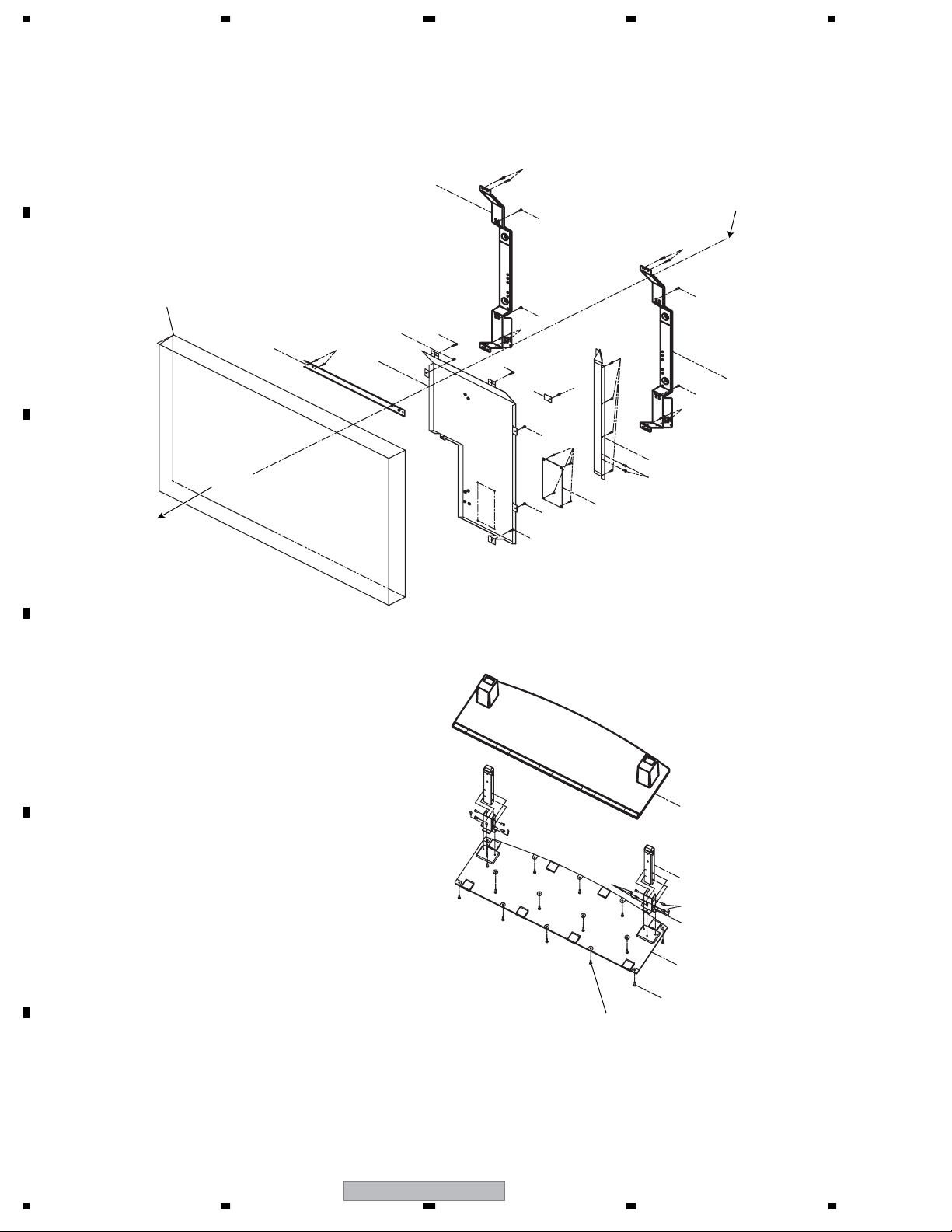
2. EXPLODED VIEWS AND PARTS LIST
NOTES:
A
Parts marked by "NSP" are generally unavailable because they are not in our Master Spare Parts List.
The mark found on some component parts indicates the importance of the safety factor of the part.
Therefore, when replacing, be sure to use parts of identical designation.
Screws adjacent to mark on product are used for disassembly.
For the applying amount of lubricants or glue, follow the instructions in this manual.
(In the case of no amount instructions, apply as you think it appropriate.)
2.1 PACKING
B
C
D
E
F
14
PDP-42A3HD
1234
Page 15

5678
PACKING PARTS LIST
No. Description Part No.
No. Description Part No.
Mark
1 Accessory Box PAU-42THD 30751-04-000
2 Remote control Unit (AXD1522) 01400-0520
3 Cable Power Cord P04117A 01300-0390
4 Bag Vinyl B (260*360*0.03) 10711-01-002
NSP 5 Battery 1.5V, AAA(ALKALINE) • • • •
6 Hook 30191-01-001
7 Manual (English) 20010-0260
NSP 8 Warranty Card 20300-0160
NSP 9 Card (Register) 20300-0170
10 Wiping Cloth 00999-0060
11 Gift Box-Bottom 30701-05-000
Mark
12 Cushion Bottom-right 30711-04-005
13 Cushion Bottom-left 30711-04-004
NSP 14 PDP-42A Set • • • •
15 Mirror Mat 30721-07-001
16 Cushion Top-center 30711-04-003
17 Cushion Top-left 30711-04-001
18 Pulp Pad Top 30740-02-001
19 Silicagel (3g) 10731-01-001
20 Gift Box-Top See Contrast table(2)
21 Cushion Top-right 30711-04-002
24 Guide Supporter-Box 30313-01-000
(2) CONTRAST TABLE
PDP-42A3HD/KUCXKA, /KUCXC and PDP-4214HD/KUCXC are constructed the same except for the following :
Mark No. Symbol and Description
20 Gift Box-Top 30701-04-001 30701-04-001 Not used
20 Gift Box-Top Not used Not used 30701-04-002
PDP-42A3HD
/KUCXKA
PDP-42A3HD
/KUCXC
PDP-4214HD
/KUCXC
A
B
C
D
>
E
56
PDP-42A3HD
F
15
7
8
Page 16
1234
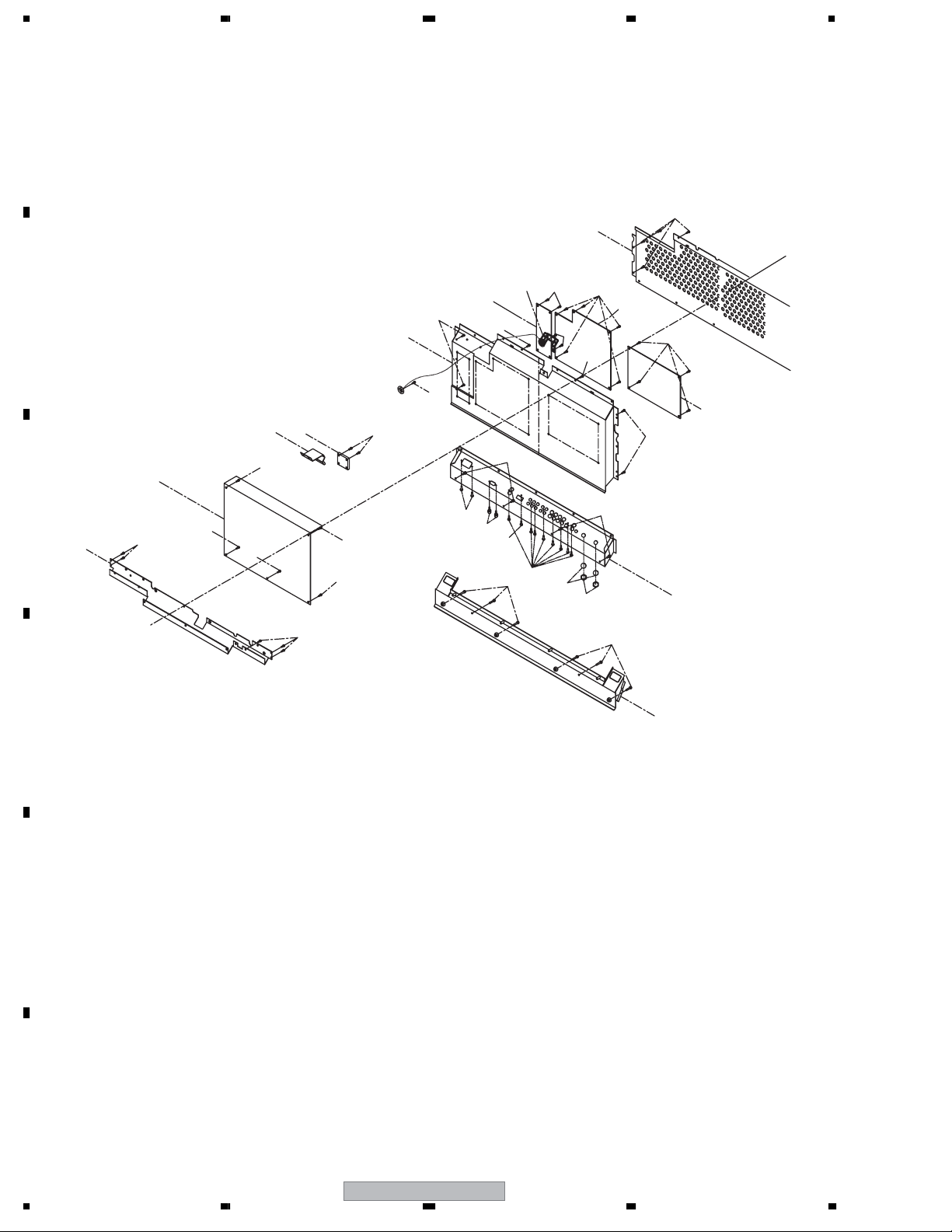
2.2 EXTERIOR SECTION (1)
A
5
8
To "2.3 Exterior Secton(2)
10
5
14
15
10
9
10
5
B
C
2.4 Front Panel
D
PDP Panel
Section
10
5
2
3
7
4
5
5
18
13
6
13
6
5
16
1
21
24
E
26
F
16
1234
PDP-42A3HD
25
24
23
22
26
Page 17
5678
EXTERIOR SECTION (1) PARTS LIST
Mark No. Description Part No.
1 SUB AV & AMP Assy 220-2050
2 BRKT SMPS-N 30168-01-000
NSP 3 Screw M4x10, SEMS, FNI • • • •
4 SHIELD SIDE 30103-02-000
5 Screw T4x16, 2S, T/T,BH,BLK M1305401617
6 Screw M4x8,BH,BLK M1015400817
NSP 7 Screw M4x10, SEMS,FNI • • • •
8 ASS’Y BRKT V-SUPPORTER-L 01433-0040
9ASS’Y BRKT V-SUPPORTER-R 01433-0050
NSP 10 Screw M5x12, SEMS, FNI • • • •
11 • • • •
12 • • • •
13 Screw M3x8, SEMS, ZNW M1040300815
14 BRKT SIDE AV-USA 30166-02-001
Mark No. Description Part No.
15 Screw T3x8, 2S, T/T,BH,BLK M1305300817
16 Screw M4x8, SEMS, ZNW M1040400815
17 • • • •
18 SENSOR Assy 010-2742
19 • • • •
20 • • • •
21 ASSY STAND See Contrast table(2)
22 ASSY BRKT BASE 01433-0090
23 BRKT LEG SUPPORTER 30169-01-000
24 Screw M4x8, SEMS, BLK M1040400815
25 ASSY STAND LEG 01425-0020
26 Screw T4x10, 2S,T/T M1308401017
(2) CONTRAST TABLE
PDP-42A3HD/KUCXKA, /KUCXC and PDP-4214HD/KUCXC are constructed the same except for the following :
Mark No. Symbol and Description
21 ASSY STAND 01425-0030 01425-0030 01425-0040
PDP-42A3HD
/KUCXKA
PDP-42A3HD
/KUCXC
PDP-4214HD
/KUCXC
A
B
C
D
E
56
PDP-42A3HD
F
17
7
8
Page 18
1234
2.3 EXTERIOR SECTION (2)
A
B
10
21
To "2.5 Rear Section
10
11
4
10
9
10
12
10
3
10
10
C
22
To "2.2 Exterior Section(1)
D
10
12
10
10
8
18
19
18
20
16
17
10
14
16
16
14
13
7
6
1
10
10
10
10
2
15
E
F
18
1234
PDP-42A3HD
Page 19

5678
EXTERIOR SECTION (2) PARTS LIST
Mark No. Description Part No.
1 SMPS Assy 150-2040
2 DTT_ANALOG Assy 010-2640
3 DIGITAL Assy 010-2741
4 EMI FILTER PCB Assy 150-2050
5• • • •
6 BRKT FAN-TOP 30172-01-001
7FAN D05X12TL(50x50x10) 10511-07-001
8 Screw M3x12, SEMS,ZNW M1040301215
9 ASSY SHIELD MAIN 01434-0010
10 Screw M4x8, SEMS,ZNW M1040300815
11 BRKT N-FILTER 30173-01-000
12 Screw M4x6, SEM(E),ZNW M1033400615
13 BRKT REAR BOTTOM 30104-03-001
14 Screw T4x16,SS,T/T,BH,BLK M1305401617
15 BRKT MAIN AV-USA 30165-02-001
16 Screw T3x8,2S,T/T,BH,BLK M1305300817
17 Screw M3x8,3S,HH,FNI M1116300805
18 Screw M4x8,BH,BLK M1015400817
19 Wsher (Ø10) M1231111002
20 NUT UNF 3/8INCH832 M1211210002
21 ASSY SHIELD MAIN TOP 01434-0020
22 ASSY BRKT MAIN SUPPORTER 01433-0060
A
B
C
D
E
F
56
PDP-42A3HD
19
7
8
Page 20
1234
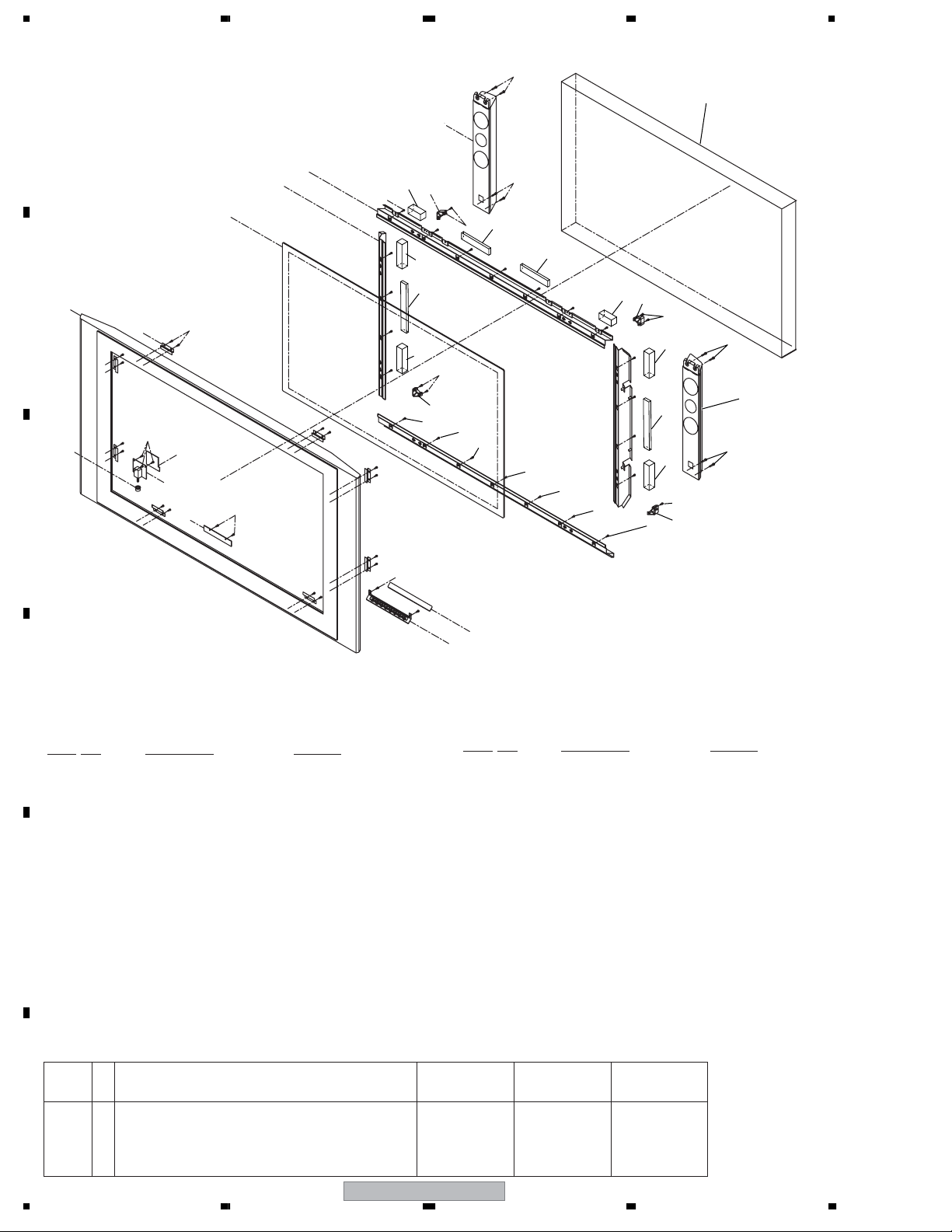
2.4 FRONT PANEL SECTION
A
18
PDP PANEL
16
12
13
21
14
5
11
15
22
20
1
B
10
5
22
19
18
19
21
14
22
15
18
15
14
5
3
4
2
5
C
6
5
5
5
5
5
5
20
22
15
14
5
17
18
9
8
7
D
FRONT PANEL SECTION PARTS LIST
Mark
Mark No. Description Part No.
1 ASSY CABINET FRONT See Contrast table (2)
2POWER SW Assy 150-2040
3 KNOB POWER See Contrast table (2)
4 INSULATION SHEET-POWER 30321-01-000
5 Screw T3x8,2S,T/T,BH,BLK M1305300817
6 CONTROL IR & LED Assy 220-2060
7 KNOB CONTROL See Contrast table (2)
E
8 SUB KEY Assy 220-2040
9
10 ASSY BRKT FILTER GUIDE-L 01433-0010
11 PDP OPTICAL FILTER 05100-0020
Screw T3x12,2S,T/T,BHW,ZNW M1308301215
No. Description Part No.
12 ASSY BRKT FILTER HOR 01433-0020
13 ASSY BRKT FILTER VER 01433-0030
14 GUIDE PANEL-N 30297-01-000
15 Screw M3x6,FH,ZNW M1011300615
16 SPEAKER(With wire assy:1170) 02400-0060
17 SPEAKER(With wire assy:350) 02400-0050
18 Screw T4x14,2S,T/T,PHW,ZNW M1308401415
19 EMI GASKET (45*10*1.0) 30501-05-006
20 EMI GASKET (100*10*1.0) 30501-05-007
21 EMI GASKET (40*10*10T) 30501-05-008
22 EMI GASKET (110*15*15) 30501-05-009
(2) CONTRAST TABLE
PDP-42A3HD/KUCXKA, /KUCXC and PDP-4214HD/KUCXC are constructed the same except for the following :
Mark No. Symbol and Description
F
1 ASSY CABINET FRONT (42A3HD) 01421-0130 01421-0130 Not used
1 ASSY CABINET FRONT (4214HD) Not used Not used 01421-0140
3 KNOB POWER 30251-04-001 30251-04-001 30251-04-002
7 KNOB CONTROL 30252-04-001 30252-04-001 30252-04-002
20
1234
PDP-42A3HD
/KUCXKA
PDP-42A3HD
PDP-42A3HD
/KUCXC
PDP-4214HD
/KUCXC
Page 21

5678
2.5 REAR SECTION
3
2
1
To "2.3 Exterior Section(2)
5
5
4
5
5
6
7
2
8
5
5
6
7
9
5
5
5
5
A
B
C
REAR SECTION PARTS LIST
Mark
No. Description Part No.
1 ASSY SHIELD MAIN TOP 01434-0020
2 Screw M3x8,SEMS,ZNW M1040300815
3 ASSY REAR BACK 01428-0020
4 Screw M4x8,BH,BLK M1015400817
5 Screw T4x16,2S,T/T,BH,BLK M1305401617
Mark No. Description Part No.
6RUBBER CAP 30602-01-001
7 Screw M4x12,SEMS,BLK M1040401217
8 ID Label See Contrast table (2)
9Warning Label 20500-0990
(2) CONTRAST TABLE
PDP-42A3HD/KUCXKA, /KUCXC and PDP-4214HD/KUCXC are constructed the same except for the following :
Mark No. Symbol and Description
8 ID Label 20500-0980 20500-0980 20500-1000
PDP-42A3HD
/KUCXKA
PDP-42A3HD
/KUCXC
PDP-4214HD
/KUCXC
D
E
56
PDP-42A3HD
F
21
7
8
Page 22

1234
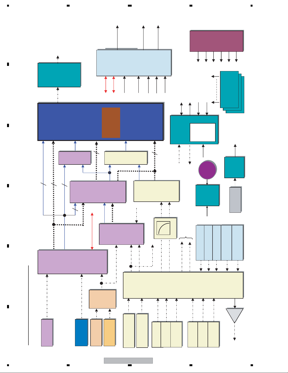
3. BLOCK DIAGRAM AND SCHEMATIC DIAGRAM
3.1 BLOCK DIAGRAM
3.1.1 OVERALL BLOCK DIAGRAM
A
B
C
D
E
F
22
1234
PDP-42A3HD
Page 23
5678
ATS
/PDIF
3.1.2 ATSC BLOCK
ATSC BLOCK
+3.3V
+A6VCC
. DC-DC
Converter
+2.5V
+1.2V
+3.3V
+5.0V
+2.5V
+2.5V
Linear Reg.
+1.2V
Communication
UART0 (Commu nication)
UART1 (RS232C)
A
To Disp lay Board
L/R ATSC
IIS (ATSC)
ATSC YPbPr Out
UART2 (RS232C)
For Deb ug
ATSC CVBS Out
(720P/108 0i)
DAC
DAC
Audio
Audio
Digital-
Digital-
S/PDIF Out
SW
SW
B
3
C S/PDIF
ATS
C
Flash
EEPROM
4MByte
16KB
150
150
MDIN
MDIN
CPU
(TL955B2-SH)
Channel
Decoder
Digital
Tuner
DDR SDRM
32MByte
Analog
D
DDR SDRM
32MByte
E
Tuner
CVBS NTSC
SIF_A
ATSC
ATSC
Jack Ant
56
PDP-42A3HD
7
NTSC
NTSC
F
23
8
Page 24
1234
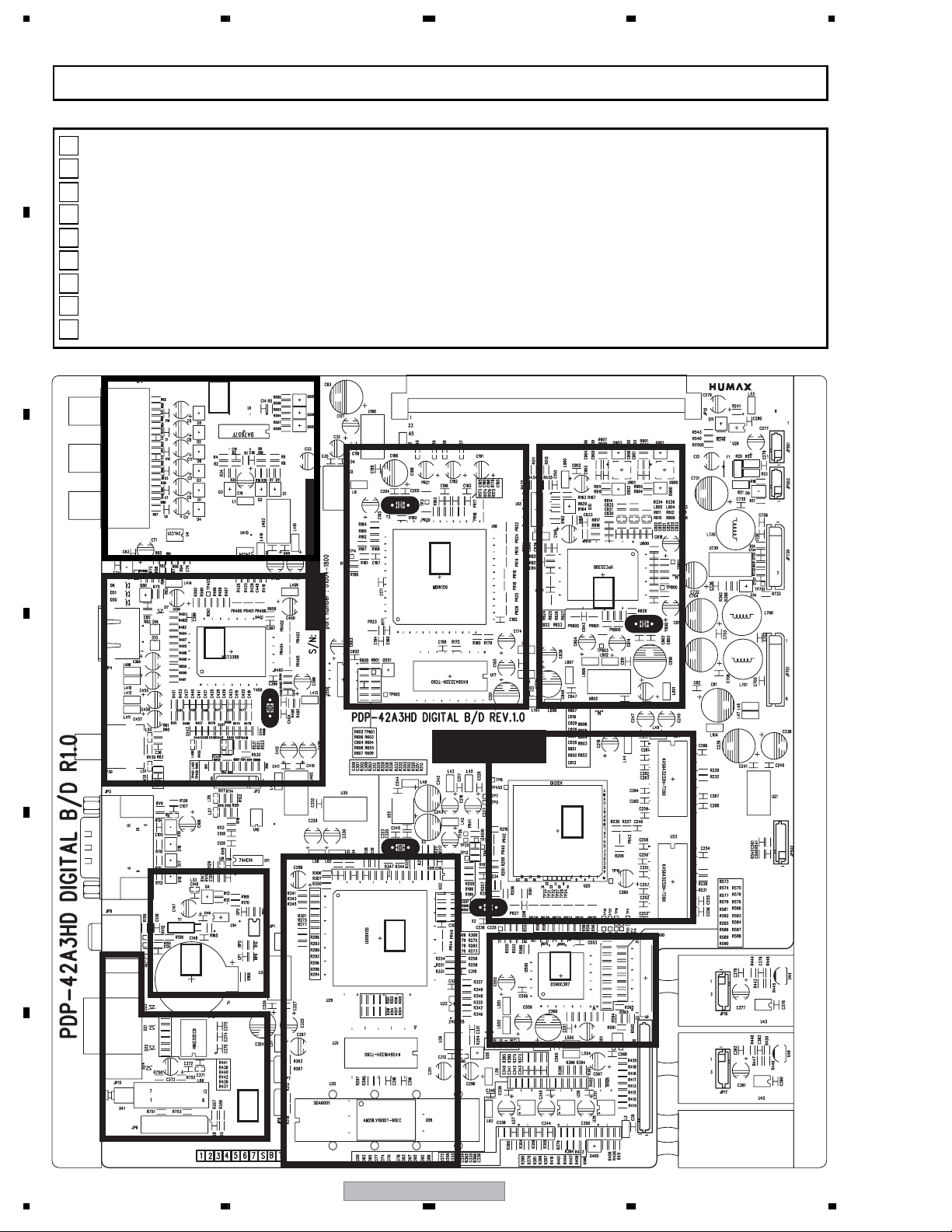
1. Digital PCB Block Explanation
A
A : Component Video input Block(BA7657)
B : ADC and HDMI receiver Block(MST3388M)
C : Real Timer Block(M41T81)
D : RS232 communication part
E : Micom Block(SDA6001+K4S641632H-TC60+AM29LV160DT)
F : Deinterlace Block(MDIN150+K4S643232H-TC60)
G : Sub-Video Decoder Block(VPC3230)
H : Scaler Block(ASI510)
B
I : LVDS transmitter Block(DS90C387)
A
C
F
G
B
D
H
E
E
C
I
F
24
1234
D
PDP-42A3HD
Page 25

5678
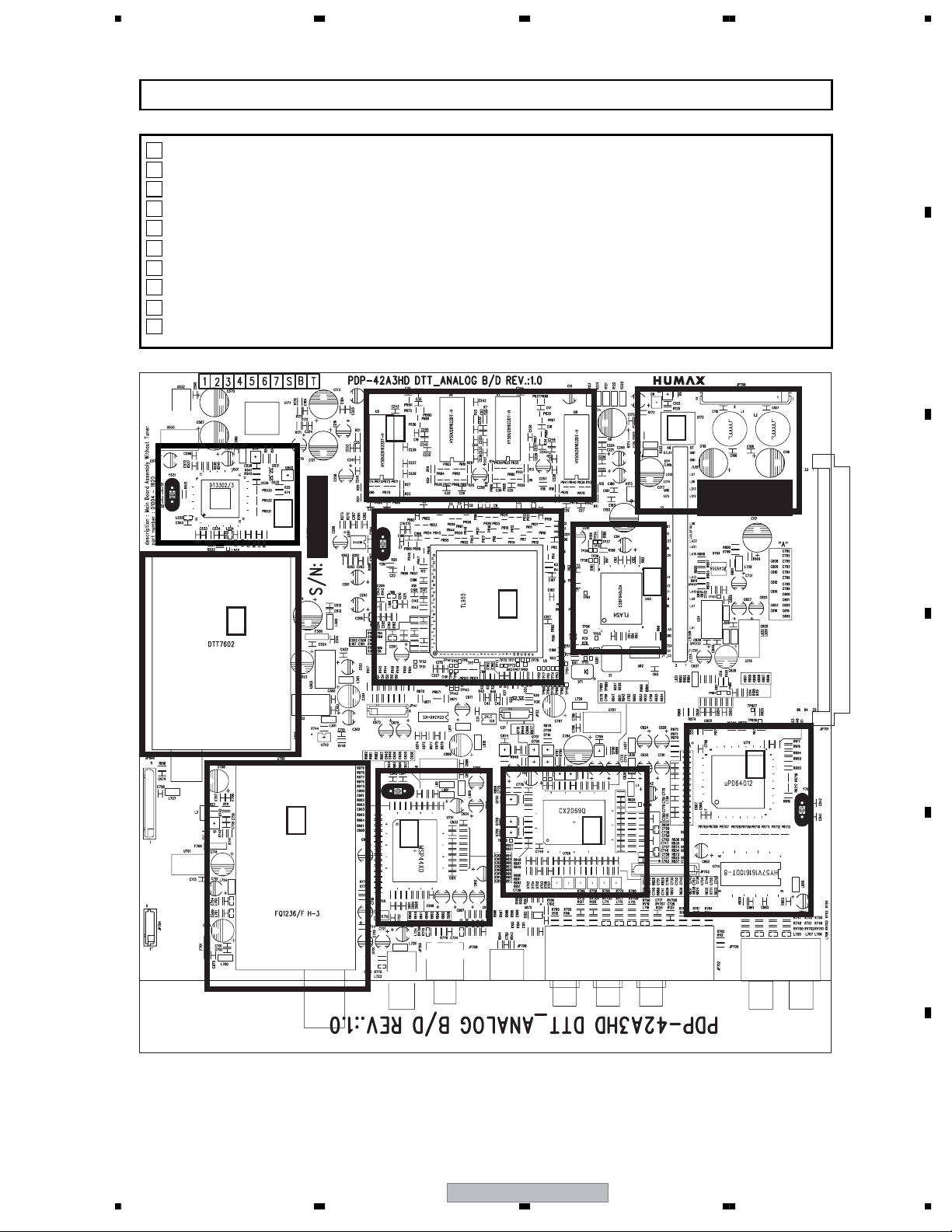
Block Description of DTT
A
1. DC-DC Block is composed of Regulators(BA05(5V), LP3965ES(1.2V), LP2995MX(VREF,VTT)) and
SMPS powers(2V5VCC,3V3VCC,A6VCC).
2. UART Communication is composed of UART1(Communication), UART2(RS232), UART3(RS232 for
debug)
3. The EEPROM block stores the current states, channels, and other user setting values.
B
4. The Flash Rom block stores operation source.
5. ATSC input block is composed of Digital tuner(DTT7608) and channel Decorder(LGDT3303).
6. NTSC input block is composed of Analog Tuner and connects in Video decorder(uPD64012).
7. DDR SDRAM block is composed of 4 32MByte and stores the current Video and information
instantly.
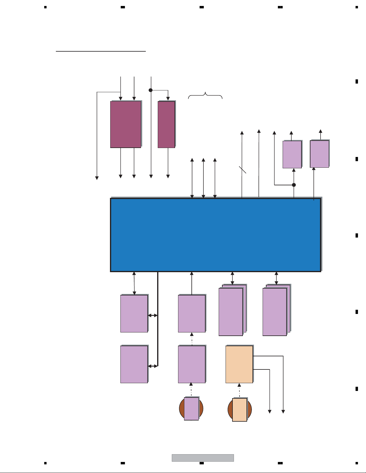
8. The CPU block functions MPEG decoder, converts the video format and control the related IC.
C
9. The Audio DAC converts from IIC Audio to L/R Analog Audio.
10. The SPDIF outputs 5.1Ch Dolby Digital audio signal.
D
56
PDP-42A3HD
E
F
25
7
8
Page 26
1234
LI
NE_OU
3.1.3 DISPLAY BLOCK
A
P
L/R SC2
(CXA2069)
L/R Aux.
(Headp hone)
L/R Main
(Power Amp)
. M7V
. A6VCC
. A12VCC
. 12VCC
. 2V5VCC
. 3V3VCC
Audio
(2069,
Audio
J-
J-
L003
L003
LVDS Tx
DS90C387
150
150
MDIN
D-INO[23:0]
24
MDIN
HDMI I2S
150
B
C
(~DE)
4
D
D- H/ V Sync & clk
30
A-INE[23:0]
5
24
(~ SOG)
8 Bit
4
MDIN
A- H/ V Sync & c lk
MUX
(2069,
ATSC I2S
ASI510
(Scaler)
8 Bit
(I/P)
Audio
MSP44X0,
4052)
MSP44X0,
4052)
SIF _A
L/R Main
(CXA2069)
V-H/ V Sync & clk
MUX
For CC
RGB/FB
MSP44X0
L/R ATSC
L/R DTV2
L/R DTV1
V-IN [ 15:0]
16
VPC3230
(Decode)
IIC
SDA6000M
MICOM_CVBS
LED
RGB/FB
Key
Tele-t ext
Rx/Tx
I/R
IIC
Real
Real
C/C
5Vst
Bat.
Bat.
Timer
Timer
(M41T81)
(M41T81)
I/O
Expender
Rx/Tx
232C
MAX232
MAX232
RS232C
RS232C
LPF
uPD
RGB
9886
9886
MST3388
E
F
HDMI
HDMI
-11 0
HDMI I2S & S/ PDIF
ATSC
ATSC
7657
BA7657
YPbPr 1
YPbPr 1
7657
Display BLOCK
26
1234
(Video
64012
~ 480P
CVBS1
YPbPr 2
YPbPr 2
PDP-42A3HD
Decode ,
C/C & 3D)
C2
MICOM_CVBS
CVBS2/ Y2
CVBS 2
CVBS 1
CVBS 2
CVBS 1
Y1/C1
ATSC_CVBS
NTSC_CVBS
ATSC_CVBS
NTSC_CVBS
To MSP
Audio L- Main
Audio R-Main
(A_S/W)
CXA2069
Y/C 1
CVBS 3
CVBS 3
Y/C 1
L/R SC2
L/R SC2
Y/C 2
Y/C 2
L/R CVBS1
L/R CVBS1
Y/C 3
Y/C 3
L/R CVBS2
L/R CVBS3
L/R CVBS2
CVBS & Audio
L/R CVBS3
NE_OU
LI
L/R PC
L/R PC
T
Page 27
5678
2. DTT & Analog PCB Block Explanation
A : Channel Demodulator Block(LGDT3303)
B : ATSC Tuner Block(DTT7608)
C : Analog Tuner Block(FQ1236)
D : DDR SDRAM Block(HY5DU281622ET-H x 4)
E : MPEG Decoder Block(TL955B2-SH)
F : Audio Decoder Block(MSP4440)
G : Video Switch Block(CX2069Q)
H : Flash Rom Block(E28F320J3A)
I : Power input Block
J : Main Video decoder Block(uPD64012+HY57V161610DTC-7)
D
A
A
B
I
C
H
E
B
D
J
C
F
G
E
56
PDP-42A3HD
F
27
7
8
Page 28

1234
3. Digital PCB Block Explanation
A
A : Indication LED Block
B : Audio AMP Block(TA2024B)
C : AV input Block
D : Control key Block
B
A
B
C
C
D
D
E
F
28
1234
PDP-42A3HD
Page 29

5678
Block Description of Display
1. The ADC & HDMI receiver composes ADC and HDMI receiver.
2. The Video Decoder is composed of uPD64012 and VPC3230, converts from analog signal to
digital video signal.
3. The CXA2069 switches input signal and selects the signal.
4. The MDIN150 is de-interlacer, it functions that interlaced signal converts de-interlaced signal and
improves picture quality.
A
5. The ASI510 is scaler IC, scaling video signal it interfaces with related IC and outputs 24 bit RGB
format video.
The SDA6001 is composed of micom and closed caption block, it controls related IC, power on/off
6.
system, and signal flowing system.
7. IO expander functions that it increases the IO port from receiving IIC communication signal.
8. The real timer(M41T81) is timer with using the clock generator.
Factory Mode
1. The method of factory mode
• To enter the test mode press keys on Remote control in
sequence as below.
B
C
D
INPUT 0 9 1 7
•You can adjust the register of IC, but this operation is very critical in set operation.
2. Self-check mode and error code is not applicable in this set.
56
PDP-42A3HD
7
8
E
F
29
Page 30

1234
3.2 DIGITAL B/D SCHEMATIC DIAGRAM
A
DIGITAL B/D PCB
B
C
D08
T01
JP730
-N
D09
-Q
T14 T15
JP701
D
D07
-K
T03
D07
-K
T03
E
F
U2
U1
U4
D07
T02
-J
JP4
U401
D01
-A
T02 T03
D08
T02
-P
30
PDP-42A3HD
1234
Page 31

5678
D08
-L
T03 T04 T05 T06
JP701
A
B
C
U28
U29
D02
T01
D02
T01
-B
D
-B
E
D08
T02
-P
D01
T01
56
: Please refer to the diagram that corresponds to the number (and following letter).
-A
: Please refer to the troubleshooting table that corresponds with the number.
PDP-42A3HD
F
31
7
8
Page 32

1234
A
GB[0..7] 6,7
B
C
VAUPLL
VDDP VDDCVPLL
VMPLL
VDVI VADC
GB1
GB2
GB0
1 8
2 7
3 6
PR400
220*4
838281807978777662616059585756555049484746454443686970717296979899
DATA0
DATA1
VDDC
92
VDDC
75
VDDC
67
106
AVDD_PLL
123
VDDP
102
VDDP
90
VDDP
88
VDDP
86
VDDP
73
VDDP
65
VDDP
53
VDDP
39
32
126
29
4
AVDD_DVI
113
AVDD_DVI
119
HSYNC0
U401
236
GG[0..7] 6,7
GB3
GB7
GG2
GG1
GB4
GB5
GB6
GG0
1 8
2 7
1 8
4 5
PR401
DATA2
DATA3
DATA4
AVDD_AUPLL
AVDD_MPLL
AVDD_ADC
AVDD_ADC
AVDD_ADC
VSYNC0
BIN0P
BIN0N
7
3 6
2 7
3 6
4 5
PR402
220*4
220*4
DATA5
DATA6
DATA7
DATA8
DATA9
SOGIN0
GIN0P
GIN0N
RIN0P
RIN0N
8
9
1011121314151617181920
GG3
GG4
4 5
1 8
PR403
DATA10
DATA11
HSYNC1
GG5
GG6
2 7
3 6
220*4
DATA12
DATA13
VSYNC1
GG7
4 5
DATA14
DATA15
BIN1P
GR[0..7] 6,7
GR0
1 8
PR404
BIN1N
GR2
GR1
2 7
3 6
220*4
DATA16
DATA17
SOGIN1
GIN1P
GR3
GR4
1 8
4 5
PR405
DATA18
DATA19
GIN1N
RIN1P
21
GR5
GR6
2 7
3 6
220*4
DATA20
DATA21
RIN1N
GR7
4 5
DATA22
DATA23
22232425262728
G_CLKA 4,6,7
G_SOG_DE 4,7
4 5
R659 100
PR406
220*4
DATACK
SOGOUT/DE
MST3388M
BIN2P
BIN2N
SOGIN2
G_HSYNC 4,6,7
2 7
3 6
HSOUT
GIN2P
G_VSYNC 4,6,7
G_FIELD 4,6
1 8
VSOUT
FIELD/GPO
GIN2N
RIN2P
RIN2N
HDMI_DOUT 12
R497 220
AUSDO
HDMI_CLK 12
R498 100
AUSCK
R499 220
TP403 TP08
HDMI_WS 12
1
R501 220
AUWS
AMUTE
RX0N
108
R500 OPEN_100
100
109
D
R657
5VSTB
R419 OPEN_101
VDVI VDDP
I2S_MCLK 12
HSPDIF 12
C406
R656 391/F
C408 104p
R502 OPEN_100
101
120
12813641423334
REXT
MCKO
VREFP
SPDIFO
RX0P
RX1N
RX1P
RX2N
RX2P
RXCKN
111
112
114
115
117
OPEN_101
C407 104p
VREFN
RXCKP
118
124
C448 104p
R429 101
HDET_PWR1
105p
A0
DDCSCL
DDCSDA
125
R658
R426
R425
MCL
103
103
103
MDA
INT
SCL
403738
U410
C404 220p
XOUT
SDA
123
A0A1A2
VCC
SCL
WP
865
7
14.31818MHz/20pF
Y400
XIN
HWRESET
35
4
VSS
CAT24WC08W
SDA
C405 220p
GND
GND
GND
GND
GND
GND
GND
GND
GND
GND
GND
GND
GND
GND
GND
GND
GND
NC
NC
NC
NC
NC
NC
NC
NC
NC
NC
127
122
116
110
107
105
104
103
91
89
87
74
66
54
31
30
5
121
95
94
93
85
84
64
63
52
51
A
E
F
D01
32
R483 100
R489 100
R485 100
R484 100
R453 OPEN_102
OPEN_103
R454
C444
OPEN_221p
R452 OPEN_101
PC_Vin1
R451 OPEN_102
222
R131
C443
OPEN_330p/50V
OPEN_CIL10J1R8KNC
L400
PC_Hin
R521 OPEN_000
R482 100
C422
680
C419 102p
R474 391
000
R481 100
RX0-1
RX0+1
RX1-1
473p
R476
473p
C420 473p
C417
R478 680
C418
R477 330
OPEN_221p
R528
M_COMP_Y
C424 473p
C426 473p
C431 473p
R466 330
000
DTT_PbX
C425 102p
R470 391
R530 000
C445
R526
R472 680
R471 330
C427
DTT_YX2
C430
R468 680
OPEN_221p
OPEN_221p
473p
C429 473p
R469 330
000
DTT_PrX
R527
473p
R475
000
M_COMP_Pb2
C446
C423
330
C421
OPEN_221p
R531
473p
C428
680
R473
OPEN_221p
M_COMP_Y 2
R520 OPEN_000
C437 473p
M_COMP_Pb 2
R455 330
R523 OPEN_000
PC_Bin
C438
C440 102p
R456 391
R486
PC_Gin1
C441 473pR457 330
OPEN_221p
OPEN_000
R460 680
C436 473p
C439
C442 473p
R458 680
OPEN_221p
C435 473p
R459 330
R524 OPEN_000
PC_Rin
C447
OPEN_221p
R522 OPEN_000
C434 473p
R461
M_COMP_Pr
R465 102
R464
1
R462 102
680
TP402
R463
C432
L403
OPEN_CIL10J1R8KNC
1
TP401
TP08
C433
OPEN_101
TP08
330p
R467
222
103
221p
C416 473p
R479 330
000
R491 101
R488 100
R490 101
R487 100
C413
103p
RX1+1
RX2-1
RX2+1
RXC-1
RXC+1
DDC_CLK1
DDC_DATA1
R493 101
R492 101
R494 101
R496
103
R495 101
473p
HDMI_INT9
SCL05,6,10
SDA05,6,10
DVI_RESET9
C415
R480 680
C414
OPEN_221p
R529
M_COMP_Pr
PDP-42A3HD
1234
Page 33

5678
B
L57
3V3STB
2V5S
L58
MD[0..15]
L59
3V3STB
C289
C295
C294
C293
C292
C291
C290
BLM31PG601SN1
Vcc_M2
C297
C296
Vcc_AM29LV
BLM31PG601SN1
10uF/16V
104p
104p
104p
104p
104p
104p
C301
C300
C299
MA[0..20]
C298
C310
105p
123
A0A1A2
VCC
WP
U32
24LC128
865
7
3V3STB
104p
C308
KEY1 9
R304 101
R305 101
124
125
P5.0/ADC
MD8
MD9
R311
472
R310
472
C309
P5.2
KEY2 9
T_SENSE 9
R307 102
R309 102
R308 102
R306 101
P5.2
P5.3
126
127
9493979910098101
P5.1/ADC
P5.2/ADC
P5.3/ADC
P5.14/T4EUD
D10
D12
D11D8D9
67667257636256
MD13
MD10
MD12
MD11
CE_EXT
CSROM
123
JP8
MD0
2
K4S641632H-TC60
37114
U31
CLKEN
3V3STB
MICOM PCB
104p
ASI_ALE 7
R313 101
P6.2
P6.2/FIELD
P5.15/T2EUD
D13
D14
D15
51
MD14
MD15
CE_FLASH
R312
MD2
MD3
MD1
DQ0
DQ1
DQ2A5DQ3
CKE
VCC
VCC
L60
BLM18PG121SN1D
C306
104p
C305
104p
3V3STB
SCL01 12
104p
104p
104p
SDA01 12
R254 000
R251 000
87
21
123
119
116
111
106
85
69
61
53
42
32
14
C304
C303
C302
104p
104p
104p
U29
10uF/16V
Vcc_M2
R252 OPEN
R253 472
R250 472
MA18
MA17
MA0
MA1
MA4
MA3
104p
10uF/16V
BLM31PG601SN1
U28
MA2
25
24232221201918876543214817
A0
A1A2A3A4A5A6A7A8A9
VCC
37
D0D1D2D3D4D5D6D7D8D9D10
293133353840424430323436394143
AM29LV160DT-90EC
MD0
MD4
MD1
MD2
MD3
R256 472
VDDA4
VDDA3
VDDA2
VDDA1
R255 OPEN
MA5
MD5
R258 472
VDD25_2
VDD25_1
VDD33_8
VDD33_7
VDD33_6
VDD33_5
VDD33_4
VDD33_3
VDD33_2
VDD33_1
A1
36
MA0
MA1
R257 OPEN
R259 472
MA19
MA7
MA6
MD7
MD6
VS_ON
SDA0 3,5,6
SCL0 3,5,6
IR_IN 9
101
R265
P3.12
IR_IN
R264 472
R266 472
R262 472
P3.5
P3.4
P3.3
74475767778798081
P3.5/T4IN
P3.0/SCL0
P3.1/SDA0
P3.2/CAPIN
P3.3/T3OUT
P3.4/T3EUD
A2A7A6A0A4A5A3
35242637332734
MA6
MA3
MA4
MA5
MA7
MA2
R263 000
R260 472
R261 OPEN
123
JP7
MA20
MA11
MA8
MA12
MA9
MA13
MA10
A10
A11
A12
A13
D11
D12
D13
MD12
MD9
MD11
MD8
MD13
MD10
IRP_IN
101
R270
P3.13
R268 472
R269 472
R271 472
P3.6
P3.8
P3.7
P3.6/T3IN
P3.7/T2IN
A9
A8
25292839233038
MA9
MA10
MA8
MA16
R267 472
MA14
MA16
MA15
A14
A15
D14
D15
45
MD14
MD15
UART_MT 12
R276 101
R273 101
R272 472
P3.9
88
83
P3.8/MRST
P3.9/MTSR
P3.10/TxDO
A11
A10
A12
MA11
MA12
MA13
R275 472
MA17
MA19
MA18
16
9
A16
A17
A18
47
Vcc_AM29LV
R274 000
UART_MR 12
R278 472
R281 472
R279 472
P3.13
P3.15
P3.12
9182908992
P3.12
P3.15
P3.13/SCLK
P3.11/RxDO
A14/ RAS
A13
A16/P4.0
A15/ CAS
40
MA16
MA17
MA14
MA15
R277 OPEN
MA20
10
A19
A20
BYTE
RP
12
RESET#
R280 OPEN
A18/P4.2
A17/P4.1
181922
MA18
CE_FLASHWRRD
11
26
CE
WE
NC
NC
14
13
R283 101
JL_SDIJL_SCK
R282 472
567
A19/P4.3
17
16
MA19
MA20
28
OE
15
ASI_RESET 7
NBLK 11
TIME_INT 4
R286 101
R288 101
JL_SCK
NSLE
JL_SDO
R290 472
R287 472
JL_SDI
NSLE
JL_SDO
855
P2.8/EX0IN
P2.9/EX1IN
P2.10/EX2IN
A20/P4.4
CS3/P4.5
15
MD0
R289 OPEN
R284 OPEN R285 472
LDQM
CE_FLASH
RB
NSLE 11
PLE 11
NSDATA 11
R296 101
R299 101
R293 000
P2.12
P2.13
P2.14
R298 472
R295 472
R292 472
P2.13
P2.14
P2.12
91011
P2.11/EX3IND0
P2.12/EX4IN
P2.13/EX5IN
D2
71
65
MD1
MD3
MD2
R297 OPEN
R294 OPEN
R291 OPEN
WR
CLKEN
CSSDRAM
GND
27
GND
46
NSCK 11
IRP_OUT
104p
C307
R15 101
R301 472
R302 103
R303 103
BL_ON BL_ON
12
P2.14/EX6IN
P2.15/EX7IN
SDA6001
D6D4D5D1D7
D3
5870645954
MD7
MD5
MD4
MD6
R300 OPEN
UDQM
PDP-42A3HD
56
4
VSS
SCL
SDA
R315 101
R317 101
P6.3/SCL1
P6.4/SDA1
CSROM
RD
47
46
R316 000
R314 000
CSROM
RD
000
Vcc_M2
MD5
MD4
DQ4
DQ5
VCC
VCCQ
3
27
SDA3
ASI_RD 7
ASI_WR 7
R322 101
R320 101
P6.6
P6.5
P6.5/-
P6.6/SDA2
CSSDRAM
CLKEN
MEMCLK
43
44
45
R319 000
R321 220
R323 000
CLKSDRAM
CLKEN
CSSDRAM
R318
472
MD6
MD7
MD8
42444547485051
DQ6
DQ7
DQ8
VCCQ
VCCQ
VCCQ
9
43
49
C311
10uF/16V
C312
104p
R324 000
WR
MD9
SCL3
R326 000
WR
R325 000
LDQM
MD10
DQ9
CC_R 5,12
R328 000
112
R
LDQM
495048
R327 000
UDQM
MD11
DQ10
NC
CC_G 5,12
113
G
UDQM
DQ11
NC
CC_B 5,12
R329 000
114
C313 104p
MD12
C315
C314
R330 102
105
B
R331
MICOM_CVBS12
MD13
DQ12
104p
104p
CC_FB 5,12
CC_V_SYNC 5,12
CC_H_SYNC 5,12
3V3STB
R333 101
R332 101
TRIG_IN
103
102
HS
BLANK
VS/VCS
CVBS1B
CVBS1A COR
RST
73
120
121 104
R338 750
R339 000
JTAG_RST
101
C316
104p
RESET#
MA0
MD14
MD15
53
DQ13
DQ14
DQ15
VSS
VSS
VSS
VSSQ
2841546124652
C319
C318
7
OPEN_101p
C357
OPEN_101p
C354
OPEN_101p
C353
OPEN_101p
C352
C356
101p
C355
101p
OPEN_472
R345 472
R341 472
R343 OPEN_472
R340
TCK
TDO
TMS
TDI
TRIG_OUT
3
1
2
95
96
TDI
TCK
TMS
TDO
P6.0/TRIG_IN
P6.1/TRIG_OUT
CVBS2
XTAL2
XTAL1
109
108
117
R344
105
X3
6MHz/18pF
C320
200p
MA4
MA2
MA3
MA1
MA6
MA5
MA7
24
25426
29530731
A0
A1
A2
A3
A4
A6
VSSQ
VSSQ
VSSQ
104p
C322
104p
104p
32833
A7
R247 OPEN_101
R367 OPEN_101
R336 OPEN_101
R334 OPEN_101
VSSA4
VSSA3
VSSA2
VSSA1
TMODE
VSSD10
VSSD9
VSSD8
VSSD7
VSSD6
VSSD5
VSSD4
VSSD3
VSSD2
VSSD1
R347 750
C323
200p
MA9
MA8
A8
MA10
341022
A9
3
BA033CCOFP
U34
1
L61
7VSTB 3V3STB
122
118
115
110
128
107
84
68
60
52
41
31
13
86
20
MA13
MA12
MA11
3511211320
A10
A11
A12
C325
C327
OUT
Vin
C326
C324
BLM31PG601SN1
R350
LDQM
A13
4,12
100uF/16V
104p
GND
4
NC
2
104p
220uF/16V
000
MA15
MA14
UDQM
15363923184019
17
/RAS
DQML
DQMU
99,12
WR
CSSDRAM
16
/CS
/WE
/CAS
CLKSDRAM
38
CLK
A
B
C
D
E
F
D02
33
8
Page 34

1234
C
A
A_RESET 16,20
SCL01 15
SDA01 15
R923
104p
C848
R954 101
R955 101
R921 101
104p
OPEN_473
C847
SLA0
7271706968676665646362616059585756555453525150494847464544434241403938
SCL
SDA
SCL0
RSTB
DVDD1
RGRED
HD
73
VD
74
VBLK
75
FILD
76
RDEO
77
DVDD3
78
BCKM
79
DGND
80
FDIO0
81
FDIO1
82
FDIO2
83
FDIO3
84
FDIO4
85
DVDD1
86
FDIO5
87
FDIO6
88
FDIO7
89
FDIO8
90
FDIO9
91
DGND
92
DFBI
93
DYSI
94
DYMI
95
DCGI
96
DCBI
97
DCRI
98
DVDD3
99
FCKQ
100
FOCP
101
FCSI
102
DVDD1
103
TEST
104
TM0
105
TM1
106
TM2
107
SMC
108
SCKSET
AVDD1
ATS1
ATS2
AVDD3
ATS3
109
110
111
112
113
114
115
TP827 TP08
TP826 TP08
VPC_FIELDS 15
VPC_VSYNCS 15
VPC_HSYNCS 15
1
1
101*4
B
C
D
15
15
15
C114
C856
C855
C854
C853
PR719
1 8
2 7
3 6
4 5
R925 100
15
15
15
15
15
VPC_C0
VPC_C1
VPC_C2
VPC_C3
VPC_C4
VPC_C5
VPC_C6
VPC_C7
PR720 101*4
331p
OPEN
_331p
OPEN
_331p
OPEN
_331p
OPEN
_331p
4 5
3 6
2 7
1 8
4 5
3 6
2 7
1 8
C852
C851
PR721 101*4
104p
104p
R974 101
3V3U
1V5VD
104p
C850
104p
C849
R969 101
DGND
BCLK8
AGND
AGND
116
R920 000
117
VPC_CLK 15
C846
ROCK
VCLY
104p
DVDD1
VCOM1
118
119
ROY0
AVI
120
VPC_Y0 15
PR718
ROY1
ROY2
VLPF1
ASYI
121
1 8
122
VPC_Y6 15
VPC_Y7 15
VPC_Y5 15
VPC_Y4 15
VPC_Y3 15
VPC_Y1 15
VPC_Y2 15
101*4
101*4
2 7
3 6
4 5
1 8
2 7
3 6
4 5
PR717
ROFDIE
C845 104p
ROY3
ROY4
ROY5
ROY6
ROY7
ROY8
DGND
ROY9
DVDD1
ROFDIE
FCLK8
U711
uPD64012
VRB1
ACYI
VRT1
ACSI
AVDD3
VRT2
ASCI
VRB2
AGI
VCOM2
ACBI
123
124
125
126
127
128
129
130
131
132
133
FCKM
VRT3
134
XI
DGND
ABI
VRB3
135
C843
3V3U
XO
VCOM3
136
137
104p
DVDD3
SDRDQ15
AVDD3
VCOM4
138
139
104p
C844
DVDD1
SDRDQ0
SDRDQ14
ACRI
VLPF2
ARI
140
141
C842
Y700
24.576MHZ/20pF
C841
37
SDRDQ1
SDRDQ2
SDRDQ13
VRB4
VRT4
AGND
142
143
144
200p
200p
SDRDQ12
SDRDQ3
DVDD1
SDRDQ11
SDRDQ4
SDRDQ10
SDRDQ5
DGND
SDRDQ9
SDRDQ6
SDRDQ8
SDRDQ7
DVDD3
SDRWE
SDRCAS
SDRCLK
SDRRAS
SDRCKE
SDRCS
DVDD1
SDRA0
SDRA1
SDRA2
DGND
SDRA3
SDRA4
SDRA5
DVDD3
SDRA6
SDRA7
SDRA8
DGND
SDRA9
SDRA10
SDRABP
DVDD3
1V5VD
36
35
34
33
32
31
30
29
28
27
26
25
24
23
22
21
20
19
18
17
16
15
14
13
12
11
10
9
8
7
6
5
4
3
2
1
3V3U
C834
C833
C832
C831
C830
104p
104p
104p
104p
104p
101*4
PR710
101*4
PR711
101*4
PR713
101*4
PR712
4 5
3 6
2 7
1 8
4 5
3 6
2 7
1 8
4 5
3 6
2 7
1 8
4 5
3 6
2 7
1 8
4 5
3 6
2 7
1 8
4 5
3 6
2 7
1 8
4 5
3 6
2 7
1 8
4 5
3 6
2 7
PR709
1 8
101*4
PR706 101*4
PR705 101*4
SDRDQ[15..0] 19
SDRDQ15
SDRDQ0
SDRDQ14
SDRDQ1
SDRDQ13
SDRDQ2
SDRDQ12
SDRDQ3
SDRABP 19
SDRA[10..0] 19
SDRCS 19
SDRCKE 19
SDRRAS 19
SDRCLK 19
SDRCAS 19
SDRWE 19
SDRDQ11
SDRDQ4
SDRDQ10
SDRDQ5
SDRDQ9
SDRDQ6
SDRDQ8
SDRDQ7
4 5
3 6
2 7
1 8
PR708 101*4
SDRA0
PR707 101*4
SDRA1
SDRA2
SDRA3
SDRA4
SDRA5
SDRA6
SDRA7
SDRA8
SDRA9
SDRA10
E
F
D03
34
R905
R904
PR704
103*4
R903103
R902103
R964103
R131103
R130103
R129103
VDEC3V3
1V5VA
103
103
1 8
2 7
3 6
4 5
C789
104p
R972 473
104p
C807
C111
104p
C818
104p
331p
+5V
3V3VA
104p
104p
C790
C795
104p
10uF/16V
C791
C792
C793
R971 473
R970 473
C808 103p
R134 101
R132 101
R133 101
VCVBS117
104p
C809 103p
Y117
C794
104p
C810 OPEN_103p
104p
C797
104p
104p
104p
C798
C800
C799
C796
C812 103p
C106 103p
C117
Y15
104p
C814 OPEN_103p
CB15
C801
104p
C802
103p
C104
C112
C113
104p
C804
C803
331p
331p
104p
104p
C816 OPEN_103p
104p
C805
C806
103p
C105
CR15
R90
OPEN_102
R89
OPEN_102
R88
OPEN_102
C43
OPEN_104p
L4
OPEN_BLM31PG601SN1
C42
OPEN_47uF/16V
R95 000
R93 000
CC_GD CC_RD CC_BD
R91 000
OPEN_KST4403
Q5
13
2
OPEN_KST4403
Q4
13
2
OPEN_KST4403
Q3
13
2
CC_G15 CC_R15 CC_B15
R96
R94
R92
OPEN_101
OPEN_101
OPEN_101
CC_VD15
CC_HD15
R900 OPEN_101
R897 OPEN_101
R899 OPEN_101
R898 101
R896 101
R901 OPEN_101
R138,R135,R136,R13 7
R87 OPEN_000
R110 000
1
1
TP866
TP867
CC_GD
CC_BD
CC_RD
CC_FB15
TP08
TP08
PDP-42A3HD
1234
Page 35

5678
D
A6VCC
L800
HDMI_CLK 15
+5V
OPEN_BLM31PG601SN1
HDMI_WS 15
HDMI_DOUT 15
L815
L95
BLM31PG601SN1
5VAM
C898
220uF/16V
3
GND
4
OUT
NC
2
Vin
U750 OPEN_BA05CCOFP
1
C897
OPEN_104p/50V
C896
OPEN_100uF/16V
R605 101
A_RESET 16,1 8
BLM31PG601SN1
C899
C902
C901
C900
MSP_DVCC
101p
C903
104p
R604
R603
R602
47uF/16V
101p
104p
R976 OPEN_000
R975 OPEN_000
ADATAO07
A
RHP 17
LHP 17
MAIN_L
MAIN_R
C904
331p
C905
331p
RHP 17
C600
R601 OPEN_101
000
000
000
R977 OPEN_000
R979 101
R978 101
SCL115,17
SDA115,17
SCLK7
LRCLK7
LHP 17
R640 101
C601
331p
VREF2
ADR_SEL
R981 000
DACM_L
DACM_R
D_CTR_OUT1
D_CTR_OUT0
R982 OPEN_ 000
R641 101
NCNCNC
U751
0
MSP44X
NC
NC
NC
TP
AUD_CL_OUT
050p
C942
R607 OPEN_220
C943
I2S_MCLK15
R995 101
Y800
OPEN_220p
331p
R600 OPEN_101
252627282930313233343536373839
MSP4440G-QA-C13-500
DACA_L
DACA_R
24
NC
23
I2S_DA3
22
RESETQ
21
I2S_WS3
20
I2S_CL3
19
NC
18
17
16
15
14
13
12
11
10
9
8
7
6
5
4
3
2
1
NC
DVSS
DVSS
DVSS
DVSUP
DVSUP
DVSUP
ADR_CL
ADR_DA
I2S_WS
I2S_CL
I2C_DA
I2C_CL
R980
I2S_DA_IN2
ADR_WS
I2S_DA_IN1
I2S_DA_OUT
STANDBYQ
000
MSP_DVCC
R993 101
SC2_OUT_L
SC2_OUT_R
XTAL_IN
XTAL_OUT
18.432MHz/15pF
050p
C941
RSC1 17
R994 101
VREF1
TESTEN
C940 560p
C944
LSC1 17
R992 101
C906
SC1_OUT_L
SC1_OUT_R
ANA_IN-
ANA_IN2+
C939 560p
C938 560p
C937
R983
472
103p
SIF
10uF/16V
CAPL_A
ANA_IN1+
101p
AHVSUP
AVSUP
R606
472
8VCC A12VCC
C907
10uF/16V
40
CAPL_M
AVSUP
65416642674368446945704671477248734974507551765277537854795580
MAIN_SIF_IN115
R999 621
R997 621
R998 621
D5
C910
C909
C908
R996 621
ZMMC8V2
100uF/16V
104p
101p
NC
NC
AHVSS
AHVSS
AGNDC
NC
SC4_IN_L
SC4_IN_R
ASG4
SC3_IN_L
SC3_IN_R
ASG2
SC2_IN_L
SC2_IN_R
ASG1
SC1_IN_L
56
SC1_IN_R
57
VREFTOP
58
NC
59
MONO_IN
60
AVSS
61
AVSS
62
NC
63
NC
64
L801
BLM31PG601SN1
5VAM
1 2
C936
C935
C934
C933
C932
C931
105p
101p
104p
C911
C912
104p
10uF/16V
47uF/16V
104p
C914
C913
C926 105p
R984 471
R_MAIN17
10uF/16V
105p
105p
C925 105p
R985 471
L_MAIN17
C930
C929
C924 105p
331p
331p
C923 105p
R986 471
B
LDTV2 15
RDTV2 15
C
R990 471
R991 471
C916
331p
331p
C915
D
C921 105p
C919 105p
C920 105p
C922 105p
C928
331p
C927
331p
R987 471
C918
331p
C917
331p
R989 471
R988 471
E
R_ATSC7
RDTV115
L_ATSC7
LDTV115
F
56
PDP-42A3HD
D04
35
7
8
Page 36

1234
0
3.3 DTT_ANALOG B/D
A
DTT_ANALOG PCB
B
D10
-T
T16 T21
C
U261
T16 T19
U5
T16 T19U7T16
U6
D10
-S
T16 T21
D
E
F
D01
T01
: Please refer to the diagram that corresponds to the number (and following letter).
-A
: Please refer to the troubleshooting table that corresponds with the number.
U671
U751
D04
-D
T07 T08 T09 T1
36
PDP-42A3HD
1234
Page 37

5678
T19U7T16 T19U8T16 T19
D06
T14
-G
A
6
JP09
JP701
U2
U281
D09
T15
D07
T22
D08
T16
B
-Q
-I
C
-O
8 T09 T10
U31
D02
T17
-B
U706
D05
T17
-E
U711
D03
-C
T04 T05
D
T06
E
F
56
PDP-42A3HD
37
7
8
Page 38

1234
E
A
V_LINE_OUT 16
C785
105p
9VCA
Y1
R892
B
VCVBS1 18
9VCA
Q705
R890 102
C
R889
471
Q703
KST4401
9VCA
D
1 3
2
R888
621
R887 102
TP880 TP08
CVBS_CC
1
105p
471
KST4401
1 3
2
R891
621
C1 18
R895
471
Q709
KST4401
1 3
9VCA9VCA
2
R961
621
CVBS2/Y2 15
R893 102
C978
TP881 TP08
1
104p
R780
471
Q712
KST4401
1 3
2
Q711
9VCA
2
101
R847
R845
KST4401
101
R869
471
Q700
KST4401
1 3
2
R864 101
R866
R865 102
C2 15
R781
471
1 3
102
C770
104p
C769
OPEN_104p
C771
C784
C783
470uF/16V
104p
22uF/16V
R848
R878
000
9VCA
L_MAIN 20
R_MAIN 20
RHP 20
R_LINE_OUT 16
L_LINE_OUT 16
LHP 20
SDA1 15,20
47uF/16V
R853 101
47uF/16V
SCL1 15,20
R855 101
R854 101
C775
101
C774
R849 101
R851 OPEN_101
R852 101
R850 OPEN_101
D708
R856 OPEN_101
R877
103
13
BAT54
2
Q701
KST4403
13
C776
100uF/16V
R857 OPEN_000
S3
S2
S1
R876
472
13
BAT54
D709
D710
1 3
BAT54
R858 102
S4
MUTE_M16,20
E
F
D05
38
7
14
21
48
32
ADR
28
S_1
S_2
S_3
S_4
MUTE
VOUT1
49
565758
YIN1
YOUT1
55
TRAP1
COUT1
33
36
DC OUT
SCL
34
SDA
VOUT3
YOUT3
3738394041
COUT3
46
TRAP2
V/YOUT2
47
COUT2
51
CIN1
VGND
35
42
50
VCC
BIAS
AGND
525354
LOUT1
ROUT1
434445
LOUT2
ROUT2
LOUT3
ROUT3
U706
CX2069Q/QFP-64
LV6
RCVBS216
LV4Y4RV4
232425
C756 105p
LCVBS3
C757 105p
RCVBS3
LV5V5RV5
293031
C758 105p
LDVI15
C759 105p
RDVI15
59
C760 105p
L_PC15
61
C761 105p
RV6
R_PC15
S2_2
S2_3
S2_4
13
20
27
S4
S2
S3
R837 101
R836 101
R838 101
RCA_IDENT216
RCA_IDENT116
HEADPHONE_ID20
C733 105p
R821 100
P6.3
V3
V4
22
C737 105p
R825 100
RCA_CVBS3
RCA_CVBS216
V6
60
C739 105p
C738 105p
R827 OPEN_100
R826 OPEN_100
1
1
TP08
TP810
DMA_CVBSNC
PVR_CVBS
C1
C2
5
101112
P6.3
C742 105p
R829 100
R828 100
C741 105p
C740 105p
R830 100
TP800 TP08
Y_S_VHS8
C_S_VHS8
C3
19
26
P6.4
P6.5
P6.6
C745 105p
C743 105p
C744 105p
C746 105p
C747 105p
R833 100
R831 100
R834 100
R832 100
R835 100
SVHS_Y216
SVHS_Y116
SVHS_C116
SVHS_C216
SVHS_C316
SVHS_Y316
V1
V2
1
8
15
P6.2
P6.1
C736 105p
C734 105p C766
C735 105p
R822 100
R823 100
R824 100
RCA_CVBS116
A_CVBS115
A_CVBS28
RTVTVLTV
LV1Y1RV1
LV2Y2RV2
C4
C748 105p
234
646362
C773 105p
C772 105p
C749 105p
C751 105p
C750 105p
R867 000
R868 000
RSC120
LSC120
9
C752 105p
LV3Y3RV3
161718
C754 105p
C753 105p
C755 105p
LCVBS216
LCVBS116
RCVBS116
0x90h
S2_1
6
S1
C765
103p
C764
103p
C763
103p
C762
103p
R839 101
RCA_IDENT320
PDP-42A3HD
1234
Page 39

5678
F
C531
200p
105
R531
25MHZ/18pF
Y531
C532
200p
SDA
SCL
D532
TZMC5V6
1 2
LGDT3302S
pin75 : NC
pin73 : XM[0] - hi g h
pin72 : XM[1] - hi g h
R537
OPEN-000
R538
OPEN-000
R540
OPEN-000
R539
+3V3T
+1V8T
GND
NC
VDD
XM[0]
VSS33
76
VSS33
77
VSS
78
XTALI
79
XTALO
80
VDD
81
DATA[9]
82
VSS
83
DATA[8]
84
VDD
85
DATA[7]
86
VSS
87
DATA[6]
88
VDD
89
DATA[5]
90
VSS33
91
DATA[4]
92
VDD33
93
DATA[3]
94
DATA[2]
95
DATA[1]
96
DATA[0]
97
DINSEL
98
DVSS
99
DVDD
100
VREFN
VREFP
REF
123456789
U531
104p
C533
C534
R532
+1V8TA
OPEN-000
VSS
VDD
OPM
TD[3]
TD[2]
TD[1]
TD[0]
XM[1]
BIAS
AVDD
CMDC
INP
INN
AVSS
AVSS
AVD33
101112131415161718192021222324
C535
104p
104p
302
R533
R534
+3V3TA
221
221
L533
TD[4]
LGDT3303
AGND
BLM18PG300SN1D
VDD
TRST
TD[5]
VSS
TD[6]
VDD33
TMS
VDD
VSS
VSS33
TCK
TDI
TD[7]
VDD
TD[8]
TDO
R536
R535
VDD
TD[9]
VDD33
IFAGC
VSS
TD[10]
RFAGC
VSS
000
C537
622
C536
51525354555657585960616263646566676869707172737475
TD[11]
VSS33
25
nIRQ
SDA
SCL
VDD
TPCLK
VSS
TPSOP
TPVALID
VDD
TPERR
TPTATA[7]
VSS
VSS33
TPDATA[6]
TPDATA[5]
VDD33
TPDATA[4]
TPDATA[3]
VDD
TDATA[2]
TDATA[1]
TDATA[0]
VSS
I2CSEL
nRST
OPEN-103p
103p
50
49
48
47
46
45
44
43
42
41
40
39
38
37
36
35
34
33
32
31
30
29
28
27
26
LGDT3302S
pin27 :
NC
R541
R542
PR531
VSB_D0
D531
TZMC5V6
1 2
OPEN-220p
C539
C538 OPEN-220p
100
100
PR533
PR532
1 8
2 7
3 6
4 5
470*4
1 8
2 7
3 6
4 5
VSB_D5
VSB_D3
VSB_D2
VSB_D4
VSB_D1
VSB_D6
VSB_D7
470*4
470*4
1 8
2 7
3 6
4 5
A
B
C
D
G
JP709
1
2
3
4
5
6
7
8
9
2.5mm
10
11
12
5267-12A
Screw hole 5m /m
56
105p
L2
10uH/3A
C107
C110
105p
L1
10uH/3A
C108
105p
C115
470uF/16V
2V5VCC
C109
105p
L532 CIL10J1R0KNC
VIN+13
C116
470uF/16V
nRESET
CH_AGC13
VIN-13
3V3VCC
nRESET3,5,7,12
VSB_D[7..0]7
TS_FAIL
TS_VAL
VSB_FAIL6
TS_CLK
TS_SOP
VSB_VAL7
VSB_CLK7
VSB_SYNC7
E
F
D06
PDP-42A3HD
7
8
39
Page 40

1234
A
JP4
21
SHIELD2
22
SHIELD3
20
SHIELD1
B
DC1R019NDA
HP_DET
+5V
GND
DDC_DATA
DDC_CLK
CE_REMOTE
CK_SHIELD
CK+
D0_SHIELD
D0+
D1_SHIELD
D1+
D2_SHIELD
D2+
NC
CK-
D0-
D1-
D2-
19
18
17
16
15
14
13
12
11
10
9
8
7
6
5
4
3
2
1
D8 ZMMC6V2
12
HP_DET
HDMI_PWR
RXC-
RXC+
RX0-
RX0+
RX1-
RX1+
RX2-
RX2+
HDET_PWR-->HDMI_PWR
R93 102
2
2
D50
ZMMC5V6
1
1
R65 000
R66 000
D51
ZMMC5V6
D7
ZMMC5V6
12
R75 000
DDC_DATA 3
DDC_CLK 3
Q80
KST4401
1 3
R72 101
RV600
SV060314B431N
R82 102
2
C80
104p
HDMI_DET 9
R98
OPEN_103
HDET_PWR 3
HDET_OFF 9
J
H
HDMI_PWR
I
C
A6VCC
L8
BLM31PG601SN1
C32
100uF/16V
C34
104p
U2
BA05CCOFP
1
3
OUT
Vin
NC
GND
2
4
C33
100uF/16V
5VB
C35
104p
C74
104p
1
A0
2
A1
3
A2
4
VSS
AT24C08A
U4
5VSTB
VCC
WP
SCL
SDA
D15 DAN202K
1
3
2
8
7
6
5
L17
BLM18PG121SN1D
R94
101
C76 104p
R91 101
R92 101
R96
103
HDET_PWR-->5VSTB
R97
103
C71
10uF/16V
C63
104p
HDET_PWR 3
DDC_CLK 3
DDC_DATA 3
D
R6 OPEN_750
K
YPbPr1_Pr
YPbPr1_Y
R85 470
R86 470
E
YPbPr1_Pb
YPbPr2_Pr
YPbPr2_Y
YPbPr2_Pb
R87 470
R88 470
R89 470
R90 470
C6 47uF/16V
C7 104p
C8 47uF/16V
C1 104p
C2 47uF/16V
C3 104p
C4 47uF/16V
C5 104p
C9 47uF/16V
C10 104p
C11 47uF/16V
C12 104p
R5 474
P4.1
C14 471p
P4.2
P4.3
P4.4
P4.5
P4.6
U1
2
HS_DECT
3
G1
4
GND
5
B1
6
GND
7
R2
8
GND
9
G2
10
GND
11
B2
12
VD1
SUB_COMP_SEL
COMP1:HIGH
COMP2:LOW
HD_OUT
R_OUT
G_OUT
C-G-IN
SYNC_OUT
B_OUT
VD_OUT
BA7657F
HD1R1
HD2
VCC
VD2
241
23
22
21
20
19
18
17
16
SW
15
14
13
R8
R1 474
R3 102
C15
103p
OPEN_000
R9 OPEN_750
R10
OPEN_000
C16
104p
R4 OPEN_750
R2
OPEN_000
L1
C19
BLM31PG601SN1
100uF/16V
BA_SW 9
CRX
CBX
YX
5VB
R7 101
R19 101
2
R34 101
5VB
Q1
KST4401
1 3
R11
561
2
5VB
Q2
KST4401
1 3
R30
561
2
M_COMP_Pr 3
M_COMP_Y 3
5VB
Q3
KST4401
1 3
R35
M_COMP_Pb 3
F
561
D07
40
PDP-42A3HD
1234
Page 41

5678
L
C567
OPEN_10uF/16V
3V3J
L554
OPEN_BLM31PG601SN1
C568
OPEN_104p/25V
U501
8
Rin1-
Vcc
7
Rin1+
Rout1
6
NC
NC
NCGND
OPEN_DS90LV018A
1
2
3
45
RH+
RH-
RG+
RG-
RF+
RF-
RE+
RE-
RD+
RD-
RCLK+
RCLK-
RC+
RC-
RB+
RB-
RA+
RA-
MDL_ALARM9
R591
OPEN_101
R593
000
R594
000
R595
OPEN_000
R592
103
1
1
1
1
1
1
1
1
1
1
1
1
1
1
1
1
1
1
NEC PDP
JP500
1
2
TP100
3
1
4
TP101
1
5
TP102
1
6
7
8
TP103
9
TP104
10
TP105
11
TP106
12
TP107
13
TP108
14
15
TP109
16
TP110
17
TP111
18
TP112
19
TP113
20
TP114
21
22
TP115
23
TP116
24
TP117
25
TP118
26
TP119
27
TP120
28
29
30
31
GT121-31P-TD LGC 31P
JP1
M
1
2
3
4
5
6
7
8
9
10
11
12
13
14
15
16
17
18
19
20
21
22
23
24
25
26
27
28
29
30
31
C2
C1
JP2
F1 215 008 250V/8A
JP3
2
L
OPEN_X-CAP
4
OUTPUT2
INPUT2
2
2
L
OPEN_X-CAP
4
OUTPUT2
INPUT2
2
12
io
FC 51E
12
io
R1
FC 51E
620KΩ,1W
2
L
1
N
3
OUTPUT1
INPUT1
1
1
N
3
OUTPUT1
INPUT1
1
VR1
OPEN_Varistor
1
N
GNDGND2
L1
OPEN_LH612202
L2
LH612202
34
2
1
YAW396-03AV
A
B
C
U1
IG-N06AEP
C730 105p
N
JP730
5267-07A
1
2
3
4
2.5mm
5
6
R733 OPEN_101
7
+3.3V
(For NEC)
R732
105p
C737
R14 101
POWER 9
000
C733
105p
POMUTE 9,10
1
PANEL_ON 9
C734
105p
R431 OPEN_101
TP701 TP08
OP
S1
DHT-1105TABF
U281
5
VCC
4
MRB
AME8530AEEVEFX26
/RESET
RESET
GND
nRESET
1
3
2
nRESET 3,5,7 ,14
System Reset
POMUTEA
M_7V 5VSTBM_7V
L730
10uH/3A
C758
105p
5VSTBK
C44
105p
C731
470uF/16V
KEY1
KEY2
KEY2
7VSTB
C735
105p
U730
BA05CCOFP
1
Vin
R25
R26
3
OUT
NC
GND
2
4
C732
220uF/16V
C736
104p
JP4
000
000
1
2
3
4
5
2mm
6
12505WR-06A
D
E
F
56
PDP-42A3HD
D08
41
7
8
Page 42

1234
A
Q
B
3V3VCC
2V5VCC
A6VCC
C117
470uF/16V
HDMI_CLK20
HDMI_WS20
HDMI_DOUT20
I2S_MCLK20
HSPDIF7
LDVI17
RDVI17
CR18
CB18
Y18
UART0_RX3
UART0_TX3
POMUTEA20
A12VCC
5VSTB
CC_HD18
CC_VD18
VPC_C718
VPC_C518
JP701
1
2
3
4
5
6
7
8
9
10
11
12
13
14
15
16
17
18
19
20
21
22
23
24
25
26
27
28
29
30
31
32
33
34
35
36
37
38
39
40
41
42
43
44
45
46
47
48
PCN10EA-96S-2.54DS
96
1
96
95
2
95
94
3
94
93
4
93
92
5
92
91
6
91
90
7
90
89
8
89
88
9
88
87
10
87
86
11
86
85
12
85
84
13
84
83
14
83
82
15
82
81
16
81
80
17
80
79
18
79
78
19
78
77
20
77
76
21
76
75
22
75
74
23
74
73
24
73
72
25
72
71
26
71
70
27
70
69
28
69
68
29
68
67
30
67
66
31
66
65
32
65
64
33
64
63
34
63
62
35
62
61
36
61
60
37
60
59
38
59
58
39
58
57
40
57
56
41
56
55
42
55
54
43
54
53
44
53
52
45
52
51
46
51
50
47
50
49
48
49
9VCA
R_PC 17
L_PC 17
SDA01 18
SCL01 18
VPC_Y6 18
VPC_Y4 18
VPC_Y2 18
VPC_Y0 18
VPC_CLK 18
VPC_FIELDS 18
VPC_C0 18
VPC_C2 18
VPC_C4 18
VPC_C6 18
CDTT_Y 8
CDTT_Pb 8
CDTT_Pr 8
CVBS2/Y2 17
C2 17
SDA21 16
SCL21 16
UART1_TX 3
UART1_RX 3
MICOM_CVBS 17
CC_FB 18
CC_B 18
CC_G 18
CC_R 18
VPC_Y7 18
VPC_Y5 18
VPC_Y3 18
VPC_Y1 18
VPC_HSYNCS 18
VPC_VSYNCS 18
VPC_C1 18
VPC_C3 18
C
R
Q102
KST4401
1 3
OUT
1
LED_VCR
D
OUT
D17
ZMMC10V
1 2
5VSTBK
R104
LED_TV
101
D102
6
P1
M1
1
BA-2x2UW/5P
R110
472
5
NA
P2 M2
3 4
2
C109
103p
E
2
GND
R105
101
VCC
3
C151
105p
BA-2x2UW/5P
R111
472
U2
ROM-N338TC-5
C33
105p
D103
5
6
P1
NA
M1
1
C110
103p
L50
BLM31PG601SN1
R106
101
LED_DVD
1 2
D18
ZMMC10V
D104
R112
472
5
6
P1
NA
M1
1
BA-2x2UW/5P
C111
103p
5VSTBK
R107
101
D105
P2 M2
3 4
BA-2x2UW/5P
R113
LED_HDMI
Q104
2
KST4401
1 3
472
C34
105p
5VSTBK5VSTBK
P2 M2
3 4
Q103
2
KST4401
1 3
5VSTBK
5
6
P1
NA
M1
P2 M2
1
3 4
Q105
2
KST4401
1 3
C112
103p
F
D09
42
PDP-42A3HD
1234
Page 43

5678
S
TL955 Audio I2S out & Audio DAC
PR671
ADATAO020
SCLK20
LRCLK20
CLK_DAC_AUD12
nRESET3,5,12,14
4 5
3 6
2 7
1 8
470*4
R671
101
DF0 is high DF1 is low -> left justified
A5V
R670
101
U671
2
SDATA
3
SCLK/DEM1
4
LRCK
5
MCLK
6
DIF1
7
DIF0
8
DEM0
1
RST
A5V
1413
VAAGND
CS4340-KS
MUTEC
AOUTL
FILT+
REF_GND
AOUTR
A
C671
C670
47uF/16V
104p
16
C672
104p
C673
1uF/50V
VOR
VOL
C674
104p
C675
1uF/50V
R678
000
R677
000
L_ATSC 20
B
R_ATSC 20
15
9
10
VQ
11
12
C
T
+3.3V
R273
OPEN-183
PWM3
R264
273
OPEN-183
R272
C267
334p
+3.3V
C261
47uF/16V
C268
OPEN_1uF/50V
New parts for clk (VCXO,audio and others)
changing library
#3 and #4 pin
connection
C265
120p
16
X2
15
14
13
12
11
10
R268 470
R261 220
R262 220
R263 220
C262
C263
104p
104p
ACLK_S06
ACLK_S16
ACLK_S26
FS16
GPIO132 ACLKS0
GPIO133 ACLKS1
GPIO134 ACLKS2
GPIO141 FS1
S0 S1 S2 CLK 2
0 0 0 8.1 92
0 0 1 11.28 96
0 1 0 12.2 88
0 1 1 16.93 44
1 0 0 18.4 32
1 0 1 16.3 84
1 1 0 22.57 92
1 1 1 24.5 76
C264
120p
Y261
27MHz/19.5pF
U261
1
X1
2
27M
VDD
3
VI
27M
4
GND
VDD
5
S0
GND
6
S1
ACLK
7
S2
ACLK
8 9
OE ACLK
MK2745-33G
27MHz 3
+3.3V
CLK_DAC_AUD 7
ACLK 7
To audio DAC (CS4340) ACLK
To TL955
12.288MHz
D
E
F
56
PDP-42A3HD
D10
43
7
8
Page 44

1234
4. PCB DIAGRAM
4.1 DIGITAL B/D
A
B
C
D
E
F
44
1234
PDP-42A3HD
Page 45

5678
A
B
C
D
E
56
PDP-42A3HD
F
45
7
8
Page 46

1234
4.2 DTT_ANALOG B/D
A
B
C
D
E
F
46
1234
PDP-42A3HD
Page 47

5678
A
B
C
D
E
56
PDP-42A3HD
F
47
7
8
Page 48

1234
4.3 CONTRPL IR & LED, SUB_AV&, SUB_KEY, EMI and POWER B/D
A
CONTRPL IR & LED
B
SUB_AV& B/D
C
D
E
SUB_KEY B/D
F
48
PDP-42A3HD
1234
Page 49

5678
A
EMI-FILTER
B
POWER_SWITCH
C
D
E
56
PDP-42A3HD
F
49
7
8
Page 50

1234
5. PCB PARTS LIST
NOTES:
A
Parts marked by "NSP" are generally unavailable because they are not in our Master Spare Parts List.
The mark found on some component parts indicates the importance of the safety factor of the part.
Therefore, when replacing, be sure to use parts of identical designation.
Screws adjacent to mark on product are used for disassembly.
For the applying amount of lubricants or glue, follow the instructions in this manual.
(In the case of no amount instructions, apply as you think it appropriate.)
7 PDP-42A3HD/KUCXC and PDP-4214HD/KUCXC
PDP-42A3HD and PDP-4214HD/KUCXC are constructed the same except for the following:
Part No.
Symbol
B
C
D
Mark
Symbol and Description
PDP-42A3HD
/KUCXC
PDP MODULE
P01 PDP-NP42H5MF01PA/PB
PKG42H5G1
1
2
PKG42H5C1
3
PKG42H5J7
PKG42H5J8
4
5
PKG42H5J5
6
PKG42H5J6
PKG42H5E1
7
PKG42H5E1
PKG42H5E2
8
PKG42H5E2
10
PKG42H5E3
11
PKG42H5J4
12
PKG42H5J3
MISCELLANEOUS ELECTRICAL PARTS
WIRE ASSY AV SIGNAL (11P,250MM)
WIRE ASSY KEY ASSY (6P,350MM)
WIRE ASSY SMPS POWER ASSY(4P)
WIRE ASSY SMPS POWER ASSY(10P)
WIRE ASSY DIGITAL POWER ASSY(7P)
WIRE ASSY ANALOG POWER ASSY(12P)
WIRE ASSY DIGITAL POWER ASSY(8P)
WIRE ASSY AUDIO POWER ASSY(6P)
WIRE ASSY LED ASSY(15P)
WIRE ASSY AV SIGNAL (10P,400MM)
WIRE ASSY LVDS ASSY (31P,550MM)
WIRE ASSY THERMAL SENSOR ASSY(5P)
WIRE ASSY GND FILTER (1P,230MM)
WIRE ASSY P/S (2P), EMI/F(2P,510MM)
CABLE RF RCA S/T+F 50MM
9S899891
9S890002
9S899895
9S899896
9S899893
9S899894
9S899897
9S899862
9S899898
9S899863 9S899863
9S899899
9S899919
9S899918
00800-0130
00800-0140
00800-0160
00800-0170
00800-0650
00800-0660
00800-0670
00800-0680
00800-0690
00800-0700
00800-0710
00800-0720
00800-0750
00800-0760
01300-1014 01300-1014
PDP-4214HD
/KUCXC
9S899891
9S890002
9S899895
9S899896
9S899893
9S899894
9S899897
9S899862
9S899898
9S899899
9S899919
9S899918
00800-0130
00800-0140
00800-0160
00800-0170
00800-0650
00800-0660
00800-0670
00800-0680
00800-0690
00800-0700
00800-0710
00800-0720
00800-0750
00800-0760
Remarks
03B
17C-08
02A
02A
02A
02A
02A
02C
02A
02C
02A
02A
02A
P19- 2
P19- 3
P19- 4
P17-18
P17- 1
P20- 2
E
F
P20- 6
P20- 8
50
1234
PWB ASSYS
DTT_ANALOG ASSY
DIGITAL ASSY
EMI FILTER ASSY
SENSSOR ASSY
SUB AV & AMP ASSY
POWER SW ASSY
CONTROL IR & LED ASSY
SUB KEY ASSY
PDP-42A3HD
010-2640
010-2741
150-2050
010-2742
220-2050
150-2040
220-2060
220-2040
010-2640
010-2741A
150-2050
010-2742
220-2050
150-2040
220-2060
220-2040
Page 51

Symbol
5678
Part No.
Mark
NSP
Symbol and Description
MISCELLANEOUS ELECTRICAL PARTS
BATTERY 3V CR2032
CPU/PDP-42A3HD, 4214HD(DIGITAL) 010-2741 010-2741A
CPU/PDP-42A3HD,4214HD(DTT_ANALOG) 010-2640 010-2640
POWER SW/42A3HD, 4214HD 150-2020 150-2020
SUB KEY/PDP-42A3HD,4214HD 220-2040 220-2040
EMI CORE CU 0930 B 01211-0020 01211-0020 Kit
EMI CORE CU 1608 B 01211-0040 01211-0040 Kit
FAN D34666-57HUM 10511-07-001 10511-07-001 Kit
PDP-42A3HD
/KUCXC
PDP-4214HD
/KUCXC
Remarks
A
MECHANISM PARTS
ASSY CABINET FRONT
SUB STAND LEG
STAND Assy
SUB REAR BACK
ASSY BRKT FILTER GUIDE-L
ASSY BRKT FILTER HOR
ASSY BRKT FILTER VER
ASSY BRKT BASE
ASSY SHIELD MAIN
ASSY SHIELD MAIN TOP
PDP OPTICAL FILTER FG401PAA-01
BRKT REAR BOTTOM
BRKT MAIN AV-USA
BRKT LEG SUPP
BRKT FAN-TOP
BRKT N-FILTER
GUIDE PANEL-N
POWER SMPS
CABLE TIE LB-17E
WIRE SADDLE-1NB
GASKET 20*15*10T
TAPE 20*25_4.5 HOLE
ADDITONAL POST
SCREW T3x12,2S,T/T,PHW(_12),ZNW,P
SCREW T4x14,2S,T/T,PHW(_14),ZNW,P
01421-0080
01425-0020
01425-0030
01428-0020
01433-0010
01433-0020
01433-0030
01433-0090
01434-0010
01434-0020
05100-0020
30104-03-001
30165-02-001
30169-01-000
30172-01-001
30173-01-000
30297-01-000
01403-0120
30311-01-001
30312-01-000
30501-05-003
30511-02-001
30561-01-001 30561-01-001
M1308301215
M1308401415 M1308401415
01421-0100 Kit
01425-0020 Kit
01425-0040 Kit
01428-0020 Kit
01433-0010 Kit
01433-0020 Kit
01433-0030 Kit
01433-0090 Kit
01434-0010 Kit
01434-0020 Kit
05100-0020 Kit
30104-03-001 Kit
30165-02-001 Kit
30169-01-000 Kit
30172-01-001 Kit
30173-01-000 Kit
30297-01-000 Kit
01403-0120 Kit
30311-01-001
30312-01-000
30501-05-003
30511-02-001
M1308301215
B
C
D
56
PDP-42A3HD
E
F
51
7
8
Page 52

1234
Symbol
A
P15-20
P15-20
B
C
Mark
PRINTED & PACKING MATERIALS
P15- 1 ACCESSORY BOX PDP-42A3HD
P15- 1 ACCESSORY BOX PDP-4214HD 30751-04-000
Symbol and Description
PDP-42A3HD
/KUCXC
30751-04-000
Not used
GIFT BOX-TOP PDP-42A3HD
GIFT BOX-TOP PDP-4214HD
ID Label PDP42A3HD
ID Label PDP4214HD
Warning Label PDP-42A3HD 20300-0160 Not used
Warning Label PDP-4214HD Not used 20500-1010
30701-04-001
Not used
20500-0980
Not used
Part No.
PDP-4214HD
/KUCXC
Not used
Not used
30701-04-002
Not used
20500-1000
Remarks
D
E
F
52
PDP-42A3HD
1234
Page 53

5678
6. ADJUSTMENT
1. At shipment, the unit is adjusted to its best conditions. Normally, it is not necessary to readjust even if an assembly is replaced. If the
adjustment is shifted or if it becomes necessary to readjust because of part replacement, etc., perform the adjustment as described below.
2. Any value changed in Service/Factory mode will be stored in memory as soon as it is changed. Before readjustment, take note of the
original values for reference in case you need to restore the original settings.
3. Use a stable AC power supply.
6.1 ADJUSTMENT OF WHITE BALANCE
Adjustment of White Balance
1.1.1. Equipment
• MIK7255 or Pattern Generator
• CA-210 Display Color Analyzer
• Remocon.
1.1.2. Pattern adjustment
• ADC Calibration : Mik pattern #240
• Auto-Calibration Mode ; 480p/60Hz
; 720p/60Hz
; 480i/60Hz
• White Balance adjustment pattern: Mik pattern #446
• Color coordinate adjustment Mode: 720p/60Hz(Component)
Composite NTSC
A
B
C
D
1.1.3. STEP1: ADC-Calibration
1) At 480p, do Auto-Calibration of ADC-cut off & Gain(1 ) on Mosaic pattern(ex Mik pattern #240)
2) At 720p/60Hz, repeat 1)
3) At 480i, repeat 1). Keep upper sequence
1.1.4.
How to enter; TV/AV -> 0 -> 9 -> 1-> 7 (press by a second, enter factory mode)
(2) High : x=0.276 , y=0.283 +/- 0.02 (11000k)
(3) Low : x=0.313 , y=0.329 +/- 0.02 (6500k)
STEP2: Adjustment of White - Balance
1) At Component 720p/60Hz, adjust white Balance Mid , High ,Low at pattern Full white 70%
(Ex; Mik pattern #446)
2) At Composite NTSC (J), repeat 1)
3) White Balance coordination (enter White Balance in Factory Mode)
-> ASI510 W/B -> Done (it shows R,G,B adjustment toolbar)
(1) Mid : x=0.283 , y=0.298 +/- 0.02 (9300k)
56
PDP-42A3HD
7
E
F
53
8
Page 54

1234
6.2 OPERATION TEST IN EACH MODE
A
Operation test in each mode
1.2.1. Equipment
• MSPG-925FS or Pattern Generator
• Remocon.
B
1.2.2. Checking mode
Connect Pattern Generator signal to HDMI.(check HDMI mode)
1) 1280 x 720p (60Hz , 16:9 )
2) 1920 x 1080i (60Hz , 16:9 )
3) 720 x 480p (60Hz , 16:9 )
4) 720 x 480i (60Hz , 16:9 )
C
1.2.3. Check operation status
Patt. No Pattern Te st method Remark
25 Overall 1. Check video noise at high frequency.
2. Check Ringing.
3. Check diagonal line noise in all
(By changing Contrast is necessary.)
17 16 gray scale 1. Check saturation of Contrast / brightness
D
by min/max.
2. Check noise.
E
F
54
1234
PDP-42A3HD
Page 55

6.3 TV
5678
TV
1.3.1. Equipment
• FLUKE54200M01 or Signal Generator
• Remocon
1.3.2. preparing for adjustment
• Connect Signal Generator signal to Tuner Jack.
• Make TV standard to NTSC.
• Frequency.
1). VHF(L) : 83.25MHz
2). UHF : 567.25MHz
3). UHF : 729.25MHz
• Supply RF with below (multi burst + Color Bar + gray scale) signal.
1.3.3. Checking operation
Pattern Te st method Remark
Video multi burst + Color
1. Contrast, Brightness, check color spread as
A
B
C
Bar + gray scale
changed.
2. Check Sharpness.
3. Check unclearness and ringing of black Level and
white level border.
1.3.4. Checking Sound
-54200 equipment setting -> MONO; 1K, STEREO; L; 1K, R;3K , SAP ; 5K
System signal OSD setup Output (L/R) Remark
Sound
BTSC M
MONO
STEREO
MONO+SAP
MONO 1K / 1K
STEREO 1K/1K
SAP 1K/1K
MONO 1K+3K / 1K+3K L+R / 2 , L+R / 2
STEREO 1K / 3K
SAP 1K+3K / 1K+3K L+R / 2 ,L+R / 2
MONO 1K / 1K
STEREO 1K / 1K
D
E
SAP 5K / 5K
STEREO+SAP
56
MONO 1K /1K
STEREO 1K/3K
SAP 5K/5K
PDP-42A3HD
F
55
7
8
Page 56

1234
6.4 SPEAKER & INTERFACE
A
Speaker
1.4.1 Equipment
• Remocon , Oscilloscope, FLUKE54200M01
1.4.2 Preparing adjustment
• Input Sound signal
B
• Check operation
• Change Volume with Remocon.
• Check sound output on Speakers.
(Check normal waveform on a Oscilloscope)
• Select balance on menu with Remocon.
• With changing, check output of left/right Speaker.
(Check normal waveform on a Oscilloscope)
C
• Check Mute.
Interface
1.5.1 Equipment
D
• FLUKE54200M01 or Signal Generator
• Remocon , each Source input device (CVBS , S-video, Component)
1.5.2 Preparing adjustment
• Input AV Interface signal
1.5.3 Checking operation
• Select signal input source with Remocon.
• Check each Source normal operation status.
E
- Composite (RCA) operation check (picture & sound)
- S-Video operation check (picture & sound)
- Component operation check (picture & sound)
- SPDIF Output operation check
F
56
1234
PDP-42A3HD
Page 57

5678
6.5 FUNCTIONAL TEST
Functional Test
1.6.1 Equipment
• FLUKE54200M01 or Signal Generator
• Remocon
A
1.6.2 Preparing adjustment
Input each source signal
1.6.3 Checking Operation
Checking PIP, TWIN (test while main picture to ANALOG CH, sub picture to VIDEO 1)
- Keep pressing SPLIT / INPUT / SWAP KEY repeatedly and test PIP.
Checking Aspect ratio
s Input Lion pattern to AV Source.
s Press SCREEN SIZE key on the remocon.
s Zoom -> Cinema -> Full -> 4:3 -> WIDE, check operation.
Checking AV output (one between A and B would be OK)
A). – input signal to AV1
- Check normal output from TV that connect AV-Out terminal.
B). – input signal to DTV.
- Check normal output from TV that connect AV-Out terminal.
Caption test
– Press CC key on remocon.
B
C
D
- Check caption on picture.
Fan test
- Enter Factory Mode, test Fan On/Off operation
PDP-42A3HD
56
E
F
57
7
8
Page 58

1234
7. GENERAL INFORMATION
7.1 DIAGNOSIS
7.1.1 OPERATION SEQUENCE FLOW
A
Operation sequence flow (Power on –> Display on)
SMPS Power 7V on
B
Micom basic c heck
OK
po wer sign al
high( JP730)
SMPS Power High
A12VCC, A6VCC, 12VCC
3V3VCC, 2 V5VCC
Micom uploads source
C
D
E
program t o SDRAM(U31)
from f lashrom(U28)
Micom reads the EEPROM
data in U32
Mic om c ommunic ates
connect ed IC
Mic om set the IC register
in last stored
EEPROM settings.
Each IC communica tes
con nect ed IC.
Scaler IC(ASI510)
outputs OSD and
Vid eo siganl
LVDS Transmitter
transfer LVDS signal
to PDP Module
Mod ule D ig ital Board
con verter LVDS signal
to TTL signal
F
Module display
on
58
1234
PDP-42A3HD
Page 59

5678
Operation sequence flow (DTV mode detection –> DTV display)
+3.3V inpu ts
the MPEG Deco rder
+2.5V inpu ts
the DDR SDRAM
and MPEG De corder
+1.2V inpu ts
the MPEG Decorde r(TL955)
TL955 com munica ted
connec ted IC
A
B
TL955 upl oads
the F/W source
in Flashrom (U40)
TL955 reads the EEPROM
data in U31
TL955 s et the IC
in last stored
EEPROM sett ings.
TL955 Comunicates
LGDT3303(U531)
to find ch da ta.
The VSB signal from U531
co nvert YPbPr output
through t he TL955
The YPbPr sign al go es
to ADC(MST33 88M),
it conv erts RGB format
DTV dis play
on
Module Digital Board
con verter LVDS signa l
to TTL signal
LVDS Transmitter
transfer LVDS signa l
to PDP Modul e
C
D
E
RGB signal goes
to deinterlacer(MDIN150)
MDIN out put signal to
Scaler IC(ASI510)
PDP-42A3HD
56
F
59
7
8
Page 60

1234
7.1.2 TROUBLE SHOOTING METHOD
Trouble shooting Method (Basic fuction Test)
A
Power o n
Is power supplied
properly?
B
OSD image
check
Does OSD image
Properly?
Power check
Micom & Scaler
Bloc k check
C
Analog TV Check
Digital TV Check
D
E
Composite Video
Check
Component Video
Check
S- Video Check
HDMI Check
Analog TV Block Check
Digital TV Block Check
Composite Video
Block Check
Component Video
Bloc k Check
S- Video Block Check
HDMI Block Chec k
Audio Chec k
F
60
1234
1st f unc tion Test
PDP-42A3HD
Audio Block Check
Page 61

5678
Trouble shooting Method (detailed function Test)
Power on
A
CC function check
Picture Mode
Test
Sound function
Check
PIP/Twin
Check
V- chip function
Check
2nd function Test
CC Block Check
F/W Version &
Eeprom state
F/W Version &
Eeprom state
Component Video
Bloc k Check
V- ch ip Blo ck check
B
C
D
56
PDP-42A3HD
E
F
61
7
8
Page 62

1234
1. No Power
Preliminary Checkpoints
A
B
Check the condition of the input power &cable connection.
(JP730,JP701(DTT&Analog, JP709(Digital),JP230(AMP))
Check the condition of on-board regulators.
Check for short circuits between each power terminal and the ground.
No Power
When Powered ON
#1(M-7V)
at JP730
In Digital B/D
C
#3(Power)
at JP730
In digital Board
#5(POMUTE)
at JP730
In digital Board
D
#74,75
at U29
in digital B/D
The signal waveform
of X3
in digital B/D
Waveform 1
Waveform 2
Waveform 3
Waveform
4 - 1
Waveform 5
NG
NG
NG
NG
NG
Check SMPS
Check SMPS &Micom
Block(U29)
Check SMPS &Power Line
in Digital B/D
Check the state of soldering
in U401,U800,U29
Check the input power
part in U29
E
F
The data line waveform
of U28
Waveform
6 - 1
Change Digital B/D
NG
Check the U28 and
related Circuit
T01 T01
62
1234
PDP-42A3HD
Page 63

5678
A
B
<Waveform 1 >
<Waveform 2 >
<Waveform 4-1 >
C
D
<Waveform 5 >
<Waveform 3 > <Waveform 6-1 >
56
PDP-42A3HD
7
E
F
63
8
Page 64

1234
2. No HDMI Signal
Preliminary Checkpoints
A
B
Check the condition of Conection of the HDMI input Connector
Check the condition of Soldering state in HDMI input part.
Check for short circuits between each power terminal and the ground.
No HDMI
signal
#37,38
at U401
in digital B/D
C
#108,109,111,112,
114,115,117,118
DC level At U401
In digital Board
EDID data
at U4
In digi tal Board
D
No sound
in HDMI mode
Check the signal
at JP4(HDMI Connector)
Waveform 7
Waveform 8
NG
NG
NG
NG
NG
Check the state of soldering
at U401,U800,U29
Check input signal part of
U401
Check HDMI_PWR
&5VSTB
Check the EDID data
&Audio output at U401
Change JP4
E
Change Digital B/D
F
T02 T02
64
1234
PDP-42A3HD
Page 65

5678
A
B
<Waveform 7 SCL >
<Waveform 7 SDA >
C
D
E
<Waveform 8 >
PDP-42A3HD
56
F
65
7
8
Page 66

1234
3. No Component Video Signal
Preliminary Checkpoints
A
Check the condition of connectin of the input component video signal.
Check the condition of soldering state in U401
Check the short point in signal l ine.
Check for short circuits between each power terminal and the ground.
B
C
D
No Component
signal (SMPTE Color Bars)
#22,25,27
at U1
in digital B/D
The output signal
At U401
In digital Board
Dose the signal
appear at PR14~19
In digital B/D
Dose the signal
appear at
PR29,31,34,35,38,39
In digital B/D
Waveform 9
Waveform 10
Waveform 11
NG
NG
NG
NG
Check the state of soldering
at JP1 &input signal part
Check U401 and
Y400 and related circuit
Check U16 and
Y2 and related circuit
Check U20 and
X2 and related circuit
Waveform 12
Check the LVDS Cable
and JP500
in Digital B/D
E
Change Digital B/D
F
T03 T03
66
1234
PDP-42A3HD
NG
Change the LVDS Cable
&LVDS chip
Test Patterm : SMPTE Color Bats
Page 67

5678
A
B
< Waveform 9 #22 >
< Waveform 9 #25 >
< Waveform 10 >
C
D
< Waveform 11 >
< Waveform 9 #27 > < Waveform 12 >
56
PDP-42A3HD
7
E
F
67
8
Page 68

1234
4. No TV Signal
Preliminary Checkpoints
A
B
Check the condition of connectin of the input TV signal.
Check the condition of soldering state in Tuner & input part
Check the short point in signal line.
Check for short circuits between each power terminal and the ground.
No TV
signal (SMPTE Color Bars)
#63
at U706
in DTT & Analog B/D
Waveform 13
C
#119
At U711
In DTT&Analog Board
Waveform 14
Dose the signal
appear at PR22,24
25,26 In DTT&Analog
B/D
D
Waveform 11
Dose the signal
appear at
PR29,31,34,35,38,39
In digital B/D
Waveform 12
NG
NG
NG
NG
Check A_CVBS1 input
part
Check U706 &
input part of U711
Check U16 and
Y2 and related circuit
Check U20 and
X2 and related circuit
E
F
Check the LVDS Cable
and JP500
in Digital B/D
Change Digital B/D
NG
Change the LVDS Cable
&LVDS chip
T04 T04
68
1234
PDP-42A3HD
Page 69

5678
A
B
< Waveform 13 >
< Waveform 14 >
< Waveform 12 >
C
D
< Waveform 11 >
PDP-42A3HD
56
E
F
69
7
8
Page 70

1234
5. No Video Signal (CVBS)
Preliminary Checkpoints
A
Check the condition of connectin of the input CVBS signal.
Check the condition of soldering state in CVBS & input part
Check the short point in signal line.
Check for short circuits between each power terminal and the ground.
B
signal (SMPTE Color Bars)
No CVBS
#8(1),15(2),22(3)
at U706
in DTT & Analog B/D
(1):VIDEO01
(2):VIDEO01
(3):VIDEO01
NG
Check CVBS input
part
Waveform 15
C
#119
At U711
In DTT&Analog Board
Waveform 14
Dose the signal
appear at PR22,24
25,26 In DTT&Analog
D
PR29,31,34,35,38,39
Check the LVDS Cable
E
B/D
Waveform 11
Dose the signal
appear at
In digital B/D
Waveform 12
and JP500
in Digital B/D
NG
NG
NG
NG
Check U706 &
input part of U711
Check U16 and
Y2 and related circuit
Check U20 and
X2 and related circuit
Change the LVDS Cable
&LVDS chip
Change Digital B/D
F
T05 T05
70
1234
PDP-42A3HD
Page 71

5678
A
B
< Waveform 15 >
< Waveform 14 >
< Waveform 12 >
C
D
< Waveform 11 >
PDP-42A3HD
56
E
F
71
7
8
Page 72

1234
6. No Video Signal (S-VHS)
Preliminary Checkpoints
A
Check the condition of connectin of the input S-VHS signal.
Check the condition of soldering state in S-VHS & input part
Check the short poi nt in signal line.
Check for short circuits between each power terminal and the ground.
B
signal (SMPTE Color Bars)
#10,12(1),17,19(2),24,26(3)
No S-VHS
at U706
in DTT & Analog B/D
(1):S-VIDEO01
(2):S-VIDEO01
(3):S-VIDEO01
NG
Check CVBS input
part
C
#121,128
At U711
In DTT&Analog Board
Dose the signal
appear at PR22,24
D
25,26 In DTT&Analog
Waveform
16,16-1
Waveform
17,17-1
NG
NG
Check U706 &
input part of U711
Check U16 and
Y2 and related circuit
B/D
Waveform 11
Dose the signal
appear at
PR29,31,34,35,38,39
NG
Check U20 and
X2 and related circuit
In digital B/D
Waveform 12
E
Check the LVDS Cable
and JP500
in Digital B/D
NG
Change the LVDS Cable
&LVDS chip
Change Digital B/D
F
T06 T06
72
1234
PDP-42A3HD
Page 73

5678
A
B
< Waveform 16 C >
< Waveform 16 Y >
< Waveform 17 Y >
C
D
< Waveform 12 >
< Waveform 17 C >
PDP-42A3HD
56
< Waveform 12 >
7
E
F
73
8
Page 74

1234
7. No Sound DVI Audio (Sine wave input)
Preliminary Checkpoints
A
Check the condition of connectin of the input DVI Audio R/L.
Check the condition of soldering state in DVI Audio R/L &input part
Check the short point in signal line.
Check for short circuits between each power terminal and the ground.
B
No Sound in
DVI Audio R/L
#29,31
at U706
in DTT & Analog B/D
C
#56,57
At U751
In DTT&Analog Board
#11,15
At U200
D
In Audio Amp Board
#28,31,27,24
At U200
Waveform 18
Waveform 19
Waveform 20
Waveform 21
NG
NG
NG
NG
Check DVI Audio input
part
Check U706 &
input part of U751
Check U751 and
Y800 and related circuit
Check U20 and
X2 and related circuit
E
F
Change Speaker
T07 T07
74
1234
PDP-42A3HD
Page 75

5678
A
B
< Waveform 18 >
< Waveform 19 >
< Waveform 21 >
C
D
< Waveform 20 >
PDP-42A3HD
56
E
F
75
7
8
Page 76

1234
8. No Sound in CVBS (Sine wave input)
Preliminary Checkpoints
A
Check the condition of connectin of the input CVBS Audio R/L.
Check the condition of soldering state in CVBS Audio R/L & input part
Check the short point in signal line.
Check for short circuits between each power terminal and the ground.
B
No Sound in
CVBS Audio R/L
#9,11(1),16,18(2),23,25(3)
C
at U706
in DTT & Analog B/D
(1):VIDEO01 Audio
(2):VIDEO01 Audio
(3):VIDEO01 Audio
Waveform 18
NG
Check CVBS Audio input
part
#56,57
At U751
In DTT&Analog Board
Waveform 19
#11,15
D
E
At U200
In Audio Amp Board
Waveform 20
#28,31,27,24
At U200
Waveform 21
Change Speaker
NG
NG
NG
Check U706 &
input part of U751
Check U751 and
Y800 and related circuit
Check U200 and
X2 and related circuit
F
T08 T08
76
1234
PDP-42A3HD
Page 77

5678
A
B
< Waveform 18 >
< Waveform 19 >
< Waveform 21 >
C
D
< Waveform 20 >
PDP-42A3HD
56
E
F
77
7
8
Page 78

1234
9. No Audio in Component Input (Sine wave input)
Preliminary Checkpoints
A
Check the condition of connectin of the input Component Audio R/L.
Check the condition of soldering state in Component Audio R/L &input part
Check the short point in signal line.
Check for short circuits between each power terminal and the ground.
B
No Sound in
Component Audio R/L
(1):Component1 Audio
(2):Component2 Audio
#50,51(1),47,48(2)
at U751
in DTT & Analog B/D
NG
Check Component Audio
input part
C
Waveform 19
#11,15
At U200
In Audio Amp Board
Waveform 20
#28,31,27,24
At U200
D
Waveform 21
Change Speaker
E
NG
NG
Check U751 and
Y800 and related circuit
Check U20 and
X2 and related circuit
F
T09 T09
78
1234
PDP-42A3HD
Page 79

5678
A
B
< Waveform 19 >
< Waveform 20 >
C
D
E
< Waveform 21 >
PDP-42A3HD
56
F
79
7
8
Page 80

1234
10. No TV Sound (Sine wave input)
Preliminary Checkpoints
A
Check the condition of connectin of the input TV SIF.
Check the condition of soldering state in TV SIF input part.
Check the short point in signal line.
Check for short circuits between each power terminal and the ground.
B
No Sound in
TV input
#67
at U751
in DTT & Analog B/D
C
Waveform 22
#11,15
At U200
In Audio Amp Board
Waveform 20
#28,31,27,24
At U200
D
Waveform 21
Change Speaker
NG
NG
NG
Check TV SIF input part
Check U751 and
Y800 and related circuit
Check U20 and
X2 and related circuit
E
F
T10 T10
80
1234
PDP-42A3HD
Page 81

5678
A
B
< Waveform 22 >
< Waveform 20 >
C
D
E
< Waveform 21 >
PDP-42A3HD
56
F
81
7
8
Page 82

1234
11. No Caption
Preliminary Checkpoints
A
B
Check the back Solding state in 96 pin connector(JP12(Digital),JP701(DTT&Analog))
Check the CC_RD,GD,BD,FB,VD,HD signal in I C.
Check the I2C between Micom and uPD64012 or EEPROM.
Check the Flash Memory or SDRAM.
CC in Remocon is
O.K. but the CC Does
Not display
OK
V-sync
NG
NG
Check Micom CVBS
Connection part
Check the crystal(X2)
and related parts on U29
Check the Micom_CVBS
C
Check CC_R,G,B,FB,H,V-sync
D
E
(Pin 121)
of IC SDA6001(U29)
OK
of IC SDA6001(U29)
OK
Change the uPD64012
Waveform 24
R,G,B,FB,H-sync
F
T11 T11
82
1234
PDP-42A3HD
Page 83

5678
A
B
< Waveform 24 R >
< Waveform 24 G >
< Waveform 24 FB >
C
D
< Waveform 24 H-sync >
< Waveform 24 B >
PDP-42A3HD
56
< Waveform 24 V-sync >
E
F
83
7
8
Page 84

1234
12. Remocon
Remocon switch push but the key does not function
A
Preliminary Checkpoints
Check the Solder state and pin of Connector JP10
Check the Solder state in LED Board.
Check the I2C between Micom and EEPROM.
Check the Flash Memory or SDRAM.
B
Remocon is O.K. but
the Function does not
operate.
OK
Check the IR Micom(Pin 76)
C
D
of IC SDA6001(U29)
OK
Check the Micom part
(IIC Comunication, other
Control line)
OK
When you power
switch off,
the set off
OK
Exchange the Digital Board
Waveform 25
NG
NG
NG
Check Remocon output
and Power in LED Board
Exchange the IC(U29)
Exchange the IC(UP1)
E
F
T12 T12
84
1234
PDP-42A3HD
Page 85

5678
A
B
< Waveform 25 >
C
D
E
56
PDP-42A3HD
F
85
7
8
Page 86

1234
13. Key
Key switch is OK but the key does not function
A
Preliminary Checkpoints
Check the Solder state and pin of Connector JP10
Check the Solder state in Key Board.
Check the I2C between Micom and EEPROM.
Check the Flash Memory or SDRAM.
B
Control key is O.K. but
the Function does not
operate.
OK
Check the key1,key2
(Pin 124,125)
C
D
of IC SDA6001(U29)
OK
Check the Micom part
(IIC Comunication, other
Control line)
OK
Check IR processor
(UP1)
OK
Exchange the Digital Board
Waveform 26
NG
NG
NG
Check Control Key Board
and Power in LED Board
Exchange the IC(U29)
Exchange the IC(UP1)
E
F
T13 T13
86
1234
PDP-42A3HD
Page 87

5678
A
B
< Waveform 26 >
< Waveform 26-1 >
C
D
E
56
PDP-42A3HD
F
87
7
8
Page 88

1234
7.1.3 DTT BASIC INSPECTION
DTT Basic Inspection
Not Working When Powered On
A
Preliminary Checkpoints
Check the condition of the input power &cable connection. (JP709)
Check the condition of on-board regulators.
Check for short circuits between each power terminal and the ground.
B
Check the Digital Board or
C
Perform short circuit test on
SMPS
each power lines.
NG
NG
Not Working
When Powered On
OK
Check the voltage output
of JP709 & JP701.
OK
Check the voltage output
of JP709 & JP701 after
connecting them.
*JP 709
1. 3.3V
2. 3.3V
3. 3.3V
4. GND
5. GND
6. GND
7. 2.5V
8. 2.5V
9. 2.5V
10. GND
11. GND
12. GND
*JP 701
9. A6VCC
10. A6VCC
OK
Check the power line path
D
Check the soldering status of
E
Note) Please refer to the power diagram of PAU-42THD for detail power connectivity information.
Note) Each input power of DTT comes via the digital board of SMPS directly. So, please check
the digital board prior to SMPS when power input is not working properly.
from connector
to on-board regulators.
on-board regulators.
Perform short circuit test on
each power lines.
NG
NG
Check the input voltage
of on-board regulators
OK
Check the output voltage
of on-board regulators
OK
Check the power line path
from on-board regulators
to each components.
F
T14 T14
88
1234
PDP-42A3HD
Page 89

5678
7.1.4 BASIC INSPECTION
Basic Inspection
Mulfunction or Not Working of Remote Control Unit
Preliminary Checkpoints
Check the battery condition of the Remote Control Unit.
Check against the a set that works normally to see if the RCU (Remote Control Unit) is working.
Check whether the connector between Digital Board and DTT&Analog Board is connected. (JP701)
Note that DTT board does not receive the key directly from RCU. Instead, MCU of digital board
gets the keys and passes them to DTT through the UART0. (Pin 34 &35 of JP701)
Mulfunction or Not
Working of Remote
Control Unit
A
B
Check the battery of the RCU.
Check the RCU.
OK
Check the connector
(JP701)
OK
Check the UART0_RX signal
(Pin 33 of JP701)
OK
Check signal line path to the
main CPU of DTT board
(U2)
Waveform 1 (When 'OK' key is pressed)
NG
NG
NG
Replace the battery/RCU
Secure the connector
Check the digital board /
Check the IR & LED board
C
D
E
< Waveform 1 >
T15 T15
56
PDP-42A3HD
7
8
F
89
Page 90

1234
Basic Inspection
Power Supply is O.K. but the DTT Does Not Wake Up
A
Preliminary Checkpoints
Check the System Clock (27MHz)and the RESET terminal of CPU.
Check the UART communication terminals between CPU and digital board (UART0).
Check the I2C between CPU and LGDT3303 or EEPROM.
Check the Flash Memory or DDR-SDRAM.
B
Power Supply is O.K.
but the STB Does Not
Wake up
Waveform 2
Check the System
Clock 27MHz (Pin 15) of IC
C
D
E
Useful Tips
MK2475-33G (U261)
OK
Check DDR-SDRAM Clock
(Pin 45 and 46) of DDR-SDRAM
(U5, U6, U7 and U8)
OK
Check system reset of Pin1 on
U281
OK
Check RESET, CS and OE
signals of Flash Memory
OK
Check for other defective
modes
Ch:CLK, Ch2:CLK~
Ch:3.3V, Ch2:Reset
Ch1:Reset, Ch2:CS/ Ch3:OE/
Waveform 3
Waveform 4
NG
NG
NG
Waveform 5
NG
Check X-Tal(Y261) and
related parts
Check the Vref and VTT voltage
and clock of
DDR-SDRAM or related parts
Check the soldering state of
U281 or Replace U281
Check Flash Memory
(U40) or related parts
1. An Unstable 27 MHz clock may be due to defect of X-TAL or clock generator (U261). Replace the X-Tal or U261.
2. DDR-SDRAM have difference clock inputs which are positive and others are negative signal (Double Data Rate).
3. Vref and VTT are have Vcc/2 and check the power source whether defected.
4. When replacing parts, be cearful of static charges from the tip of the solder iron that can easily damage the parts.
Also, check for assembly condition, soldering condition, or for incorrect or reverse insertion of parts.
F
5. If the problems are caused by CPU, change CPU board and download Serial Number.
T16 T16
90
1234
PDP-42A3HD
Page 91

5678
A
B
< Waveform 2 > < Waveform 5 >
< Waveform 3 >
C
D
E
< Waveform 4 >
PDP-42A3HD
56
F
91
7
8
Page 92

1234
Basic Inspection
Does Not Boot after Power-On or System Reset
A
Preliminary Checkpoints
The system clock 27MHz must be stable during the System Reset or the Power On Reset.
However, if X-TAL is defective, the clock may not become stable until RESET is released.
To check reset timing, turn the main power off and back on, and check if the following waveform is maintained.
B
C
D
Check the reset signal of
Flash and Pin1 of U281
Check the soldering status
of U40(Flash Memory)
and U62
NG
Does Not Boot after
System/Power-On Reset
Check the Reset and
clock timing of CPU
OK
Check the communication
between DTT and
digital board
OK
Check Flash Memory
OK
Waveform 5
Waveform 2
Waveform 4
27 MHz Clock problemReset timing promlem
NG
NG
Waveform 6
Ch1:SLC, Ch2:SDA
Check the soldering status
of X-TAL(Y261) and U261
Check the soldering status
of JP282.
Check the digital board
Check the waveform CS
and OE of Flash Memory
Check the soldering state of
E
Useful Tips
1. The CPU have two 12C for system controller.
One is communicate with system 12C(TDA10046) and the other is communicate with serial EFPROM for storing data.
2. When the system will not operate even though the basic inspection results were normal, check Flash Memory which
contains channel data and program contents.
3. Additionally check for Local DATA and Local ADDRESS buses between CPU and Flash Memory.
4. When replacing parts, be careful of static changes from the tip of the solder iron that can easily damage the parts.
Also, check for assembly condition, soldering condition, or for incorrect or reverse insertion of parts.
F
5. If the problems are caused by CPU, change CPU board and download Serial Number.
EFPROM
NG
Check the 12C Line
(Pin 6, 5 of U31)
OK
Check for other defective
modes
T17 T17
92
1234
PDP-42A3HD
Page 93

5678
A
B
< Waveform 2 > < Waveform 6 >
< Waveform 4 >
C
D
E
< Waveform 5 >
PDP-42A3HD
56
F
93
7
8
Page 94

1234
7.1.5 CPU / SYSTEM MEMORY INSPECTION
CPU /System Memory Inspection
A
Error Occurs During S/W Installation or Update through BOOTROM Board.
System Stops During Initial Booting or Operation.
Preliminary Checkpoints
If the system does not respond even though no problem was found after basic inspection,
you need to check the flash memory that contains program codes for the proper system operation,
Flash Memory Control signals that look similar to below waveforms will be repeated.
The main cause of the problems related to System Memory (i.e.Flash and DDRSDRAM)is the soldering of parts.
B
Therefore, first check the soldering condition and the power supply of IC.
Error Occurs During S/W
Installation or Update
through BOOTROM Board.
Waveform 5
C
NG OK
Check CPU
and Flash Memory
(Incorrect insertion, poor
soldering, etc.)
D
OK OK
Re-check the basic inspection
items
E
Check Flash Access
signal CE(Pin 14), OE(Pin 54)
NG
Waveform 7
Ch:DDR0A0
CH:DDR0D0
Check the Data and
Addresses of DDR-SDRAM
Check for other defective
modes
Useful Tips
1. Check CE, OE and WE of Flash Memory when system does not operate or cannnot update for new software.
2. When the system will not operate even though the basic inspection results were normal, check Flash Memory which
contains channel data and program contents.
3. Additionally check for Local ADDRESS buses between CPU and Flash Memory.
4. Check the Memory interface of DDRSDRAM if the Flash Memory is not defected.
5. When replacing parts, be careful of static charges from the tip of the solder iron that can easily damage the parts.
F
Also, check for assembly condition, soldering condition, or for incorrect or reverse insertion of parts.
6. If the problems are caused by CPU, change CPU board and download Serial Number.
T18 T18
94
1234
PDP-42A3HD
Page 95

5678
A
B
< Waveform 5 >
< Waveform 7 >
C
D
E
56
PDP-42A3HD
F
95
7
8
Page 96

1234
7.1.6 MPEG INSPECTION
MPEG Inspection
No problems Found during Basic and CPU/System Memory Inspections, but MPEG Does Not Play.
A
- Check DDR SDRAM Interface/Transport Stream(TS).
Preliminary Checkpoints
If the system does not respond even though no problems were found during the basic inspection
and the CPU/Flash inspection, you will need to check the DDR-SDRAM interface.
Check control lines between DDR-SDRAM and CPU also data/address lines.
The main cause of the problems related to System Memory (i.e.Flash and DDR-SDRAM)is the soldering of parts.
Therefore, in the event of a problem, first check the condition of the soldering and the power supply of IC.
B
No problems Found on
during Basic/Memory
Inspections but MPEG Play
Does Not Work
Ch1:RAS/, Ch2:CAS/, Ch3:WE/
NG OK
C
Check the solding
status of DDR-SDRAM
(U5, U6, U7 and U8)
OK OK
Recheck the basic inspevtion
items
D
Useful Tips
1. Make sure that basic function of the system is normal by checking that the VFD toggles
each time you press the Front power key.
2. Check the interface between CPU and DDR-SDRAM U5, U6, U7 and U8.
The interface is composed of clock(133MHz), address, data and control signals.
3. If all connections are complete, replace the DDR-SDRAM.
4. If the problems are caused by CPU, change CPU board and download Serial Number.
Check the output of DDR
SDRAM control interface
NG
Waveform 8
Waveform 7
Check the adress and data lines
of between CPU and DDR-SDRAM
Check for other defective
modes
E
F
T19 T19
96
< Waveform 7 >
PDP-42A3HD
1234
< Waveform 8 >
Page 97

5678
7.1.7 A/ V INSPECTION
A/V Inspection
No Video Output - CVBS/YPbPr
Preliminary Checkpoints
If no video is output while the UI(User Interface)and key controls are normal,
first check the video output signal of CPU.
If no video signal found,check the TS parallel data between CPU and U531.
If no output of TS data,check the U531 and relevant components.
U2(PIN:A9):CVBS
U2(PIN:B9, C9):
S-VHS
JP141(PIN1, 3, 5,):YPbPr
Waveform 9-1 (CVBS)
Waveform 9-2 (YPbPr)
No video Output
OK
Check the Video output
of CPU
OK
Check the TS line between
CPU and U531
NG
NG
Check the path between
CPU and JP705, JP706 (Incorrect
insertion, poor soldering, short
circuits, damage, etc.)
Check the TS signal path from
tuner to U531.
A
B
C
OK
Check for other defective
Useful Tips
1. If no output of TS data but tuner is good, check the U531 and relevant components.
modes
D
E
< Waveform 9-1 >
< Waveform 9-2 >
T20 T20
56
PDP-42A3HD
7
8
F
97
Page 98

1234
A/V Inspection
No Audio Output
A
Preliminary Checkpoints
B
If no audio is output through JP800 while the system is normal, first check the
CPU AUDIO output and clock. [I2S interface ].
If no problems were found, check the U671 for Audio DAC.
No Audio Output
OK
Waveform 10
Ch1:SCLK,
Ch2:LRCLK,
Ch3:ADATA0
Check the CPU
12S output
OK
NG
(Incorrect insertion, poor soldering,
short circuits, damage, etc.)
Check the path between
CPU and Clock
C
D
Useful Tips
1. The Audio problem largely from the defect of CPU, Audio DAC or incomplete soldering of the parts located along
the audio output path.
2. Audio DAC pins represent serial data, LR clock, Bit clock and system clock, respectively.
E
Waveform 11
Check the Audio clock
Pin 9 of U261
OK
Check the Audio DAC for
U761
OK
Check for other
defective modes
NG
NG
Check the X-TAL and U261
(Incorrect insertion, poor soldering,
short circuits, damage, etc)
Check the path between
Audio DAC and CPU
(Incorrect insertion, poor solding,
short circuits, damage, etc)
F
T21 T21
98
< Waveform 10 >
PDP-42A3HD
1234
< Waveform 11 >
Page 99

5678
A/V Inspection
No digital audio output
Preliminary Checkpoints
If the SPDIF output is not working while the system is normal (Including MPEG
play and A/V output), check for any problems with the SPDIF output of CPU.
A
B
No IEC958 Digital Output
Waveform 13
Check the IEC958 output
signal J5 of U2
OK
Check for other
defective modes
NG
Check the path between
CPU and IEC958 line
(Incorrect insertion, poor soldering,
short circuits, damage, etc.)
C
D
< Waveform 13 >
T22 T22
56
PDP-42A3HD
7
8
E
F
99
Page 100

1234
7.1.8 CHANNEL INSPECTION
Channel Inspection
No Channel Locking with No Problems with Power/CPU
A
Preliminary Checkpoints
If channel locking fails even though there is no problems with the system, check
the Interface between Tuner, LGDT3303 and CPU.
B
- LDGT3303 Input Power
* +3.3V
Pin21, 35, 61, 93
* +1.8V
PIN16, 19, 32, 42, 47, 55, 63,
68, 74, 81, 85, 89, 100
Channel locking failure
Check the LGDT3303
input voltage
NG
After the basic inspection, check the
path between U501 and LGDT3303
(Incorrect insertion, poor soldering,
short circuits, damage, etc)
C
- LDGT3303 PIN26
* low : reset on
* high : reset release
- LGDT3303 Pin 79, 80
* 25MHz clock
D
- 12C CLOCK [PIN48]
- 12C DATA[PIN49]
E
Check the LGDT3303 input
Waveform 14
OK
(Reset) = high
OK
Check the LGDT3303
input clock
OK
Check the 12C control
Check other related
part
NG
NG
NG
Check the path between
CPU and LGDT3303 (Incorrect
insertion, poor soldering, short
circuits, damage, etc.)
Check the path between
LGDT3303 and X-Tal (Incorrect
insertion, poor soldering, short
circuits, damage, etc.)
Check the path between
devices the LGDT3303 and EEPROM
Also, check Incorrect insertion, poor
soldering, short circuits, damage, etc.)
Useful Tips
1. Check the power byU532 are properly provided to the U531.
2. Check the 12C interface between tuner and 10046. If no problem, inspect along the tuner output path to TDA10046.
Whether the components of R, L, C's soldering status.
3. If no problem, replace the Tuner.
4. If the problems are founded by CPU, replace the CPU board and also download SN.
F
T23 T23
100
1234
PDP-42A3HD
 Loading...