

Page 1

PIONEER CORPORATION 4-1, Meguro 1-chome, Meguro-ku, Tokyo 153-8654, Japan
PIONEER ELECTRONICS (USA) INC. P.O. Box 1760, Long Beach, CA 90801-1760, U.S.A.
PIONEER EUROPE NV Haven 1087, Keetberglaan 1, 9120 Melsele, Belgium
PIONEER ELECTRONICS ASIACENTRE PTE. LTD. 253 Alexandra Road, #04-01, Singapore 159936
PIONEER CORPORATION 2006
ORDER NO.
VOLUME
INPUT SELECT
MENU/ENTER
DOWN UP LEFT/- RIGHT/+ /EXIT
PDP-425CMX
ARP3340
PLASMA DISPLAY
PDP-425CMX
PDP-42MXE10
THIS MANUAL IS APPLICABLE TO THE FOLLOWING MODEL(S) AND TYPE(S).
Model Type Power Requirement Remarks
PDP-425CMX LUC5 AC100 - 120V
PDP-42MXE10 LDFK5 AC100 - 240V
PDP-42MXE10 YVXK5 AC100 - 240V
This service manual should be used together with the following manual(s).
Model No. Order No. Remarks
PDP-425CMX, PDP-42MXE10 ARP3341 SCHEMATIC DIAGRAM, PCB CONNECTION DIAGRAM
For details, refer to "Important Check Points for good servicing".
T-IZV MAR. 2006 printed in Japan
Page 2

1234
SAFETY INFORMATION
A
This service manual is intended for qualified service technicians ; it is not meant for the casual
do-it-yourselfer. Qualified technicians have the necessary test equipment and tools, and have been
trained to properly and safely repair complex products such as those covered by this manual.
Improperly performed repairs can adversely affect the safety and reliability of the product and may
void the warranty. If you are not qualified to perform the repair of this product properly and safely,
you should not risk trying to do so and refer the repair to a qualified service technician.
WARNING
This product contains lead in solder and certain electrical parts contain chemicals which are known to the state of California to
B
cause cancer, birth defects or other reproductive harm.
NOTICE
(FOR CANADIAN MODEL ONLY)
Fuse symbols (fast operating fuse) and/or (slow operating fuse) on PCB indicate that replacement parts
must be of identical designation.
Health & Safety Code Section 25249.6 - Proposition 65
REMARQUE
(POUR MODÈLE CANADIEN SEULEMENT)
Les symboles de fusible (fusible de type rapide) et/ou (fusible de type lent) sur CCI indiquent que les pièces
C
de remplacement doivent avoir la même désignation.
SAFETY PRECAUTIONS
NOTICE : Comply with all cautions and safety related notes
located on or inside the cabinet and on the chassis.
The following precautions should be observed :
1. When service is required, even though the PDP UNIT an
isolation transformer should be inserted between the power line
D
and the set in safety before any service is performed.
2. When replacing a chassis in the set, all the protective devices
must be put back in place, such as barriers, nonmetallic knobs,
adjustment and compartment covershields, isolation resistorcapacitor, etc.
3. When service is required, observe the original lead dress. Extra
precaution should be taken to assure correct lead dress in the
high voltage circuitry area.
4. Always use the manufacture's replacement components.
Especially critical components as indicated on the circuit
diagram should not be replaced by other manufacture's.
Furthermore where a short circuit has occurred, replace those
E
components that indicate evidence of overheating.
5. Before returning a serviced set to the customer, the service
technician must thoroughly test the unit to be certain that it is
completely safe to operate without danger of electrical shock,
and be sure that no protective device built into the set by the
manufacture has become defective, or inadvertently defeated
during servicing. Therefore, the following checks should be
performed for the continued protection of the customer and
servicetechnician.
6. Perform the following precautions against unwanted radiation
and rise in internal temperature.
• Always return the internal wiring to the original styling.
• Attach parts (Gascket, Ferrite Core, Ground, Rear Cover,
Shield Case etc.) surely after disassembly.
7. Perform the following precautions for the PDP panel.
• When the front case is removed, make sure nothing hits the
panel face, panel corner, and panel edge (so that the glass does
not break).
• Make sure that the panel vent does not break. (Check that the
cover is attached.)
• Handle the FPC connected to the panel carefully.
Twisting or pulling the FPC when connecting it to the
connector will cause it to peel off from the panel.
8. Pay attention to the following.
• Pay extreme caution when the front case and rear panel are
removed because this may cause a high risk of disturbance to
TVs and radios in the surrounding.
F
2
1234
PDP-425CMX
Page 3
5678
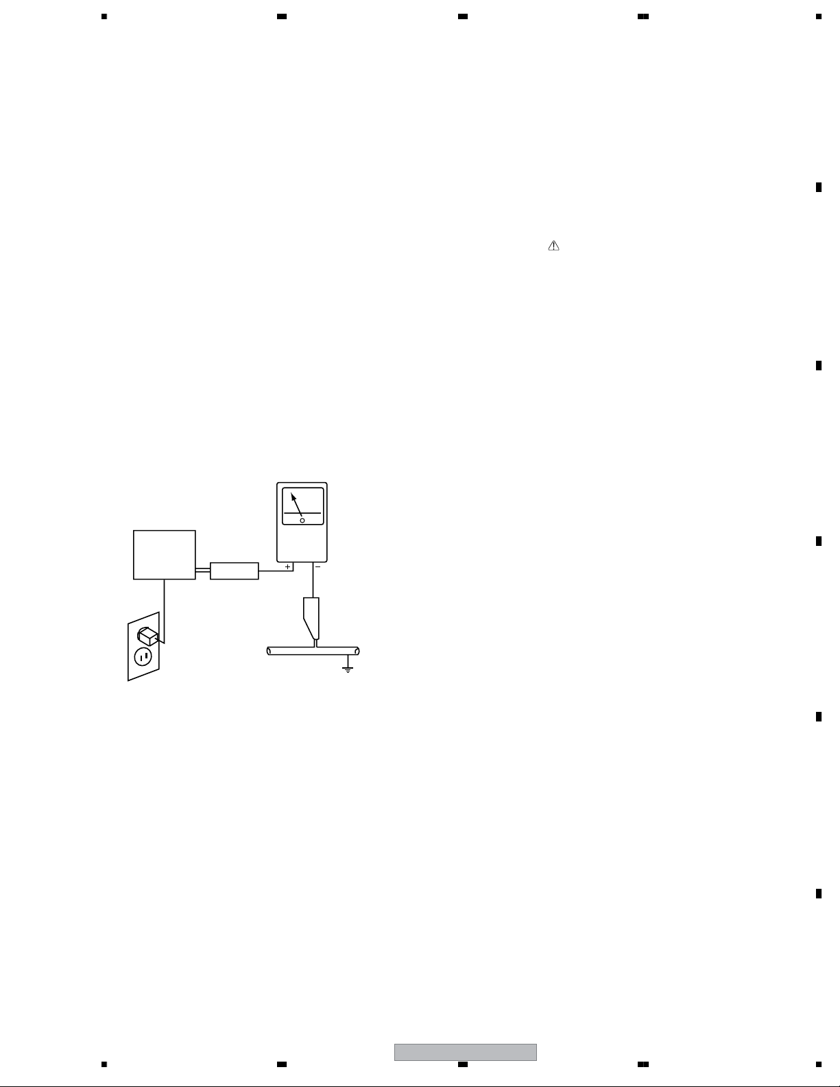
Leakage Current Cold Check
With the AC plug removed from an AC power source, place a
jumper across the two plug prongs. Turn the AC power switch on.
Using an insulation tester (DC 500V), connect one lead to the
jumpered AC plug and touch the other lead to each exposed metal
part (input/output terminals, screwheads, metal overlays, control
shafts, etc.), particularly any exposed metal part having a return
path to the chassis. Exposed metal parts having a return path to
the chassis should have a minimum resistor reading of 0.3MΩ
and a maximum resistor reading of 5MΩ. Any resistor value
below or above this range indicates an abnormality which requires
corrective action. Exposed metal parts not having a return path to
the chassis will indicate an open circuit.
Leakage Current Hot Check
Plug the AC line cord directly into an AC power source (do not
use an isolation transformer for this check).
Turn the AC power switch on.
Using a "Leakage Current Tester (Simpson Model 229
equivalent)", measure for current from all exposed metal parts of
the cabinet (input/output terminals, screwheads, metal overlays,
control shaft, etc.), particularly any exposed metal part having a
return path to the chassis, to a known earth ground (water pipe,
conduit, etc.). Any current measured must not exceed 0.5mA.
PRODUCT SAFETY NOTICE
Many electrical and mechanical parts in PIONEER set have
special safety related characteristics. These are often not evident
from visual inspection nor the protection afforded by them
necessarily can be obtained by using replacement components
rated for higher voltage, wattage, etc. Replacement parts which
have these special safety characteristics are identified in this
Service Manual.
Electrical components having such features are identified by
marking with a on the schematics and on the parts list in this
Service Manual.
The use of a substitute replacement component which dose not
have the same safety characteristics as the PIONEER
recommended replacement one, shown in the parts list in this
Service Manual, may create shock, fire or other hazards.
Product Safety is continuously under review and new instructions
are issued from time to time. For the latest information, always
consult the current PIONEER Service Manual. A subscription to,
or additional copies of, PIONEER Service Manual may be
obtained at a nominal charge from PIONEER.
A
B
C
Reading should
not be above
0.5mA
Earth
ground
Device
under
test
Also test with
plug reversed
(Using AC adapter
plug as required)
Leakage
current
tester
Test all
exposed metal
surfaces
AC Leakage Test
ANY MEASUREMENTS NOT WITHIN THE LIMITS
OUTLINED ABOVE ARE INDICATIVE OF A POTENTIAL
SHOCK HAZARD AND MUST BE CORRECTED BEFORE
RETURNING THE SET TO THE CUSTOMER.
D
E
56
PDP-425CMX
F
3
7
8
Page 4
1234
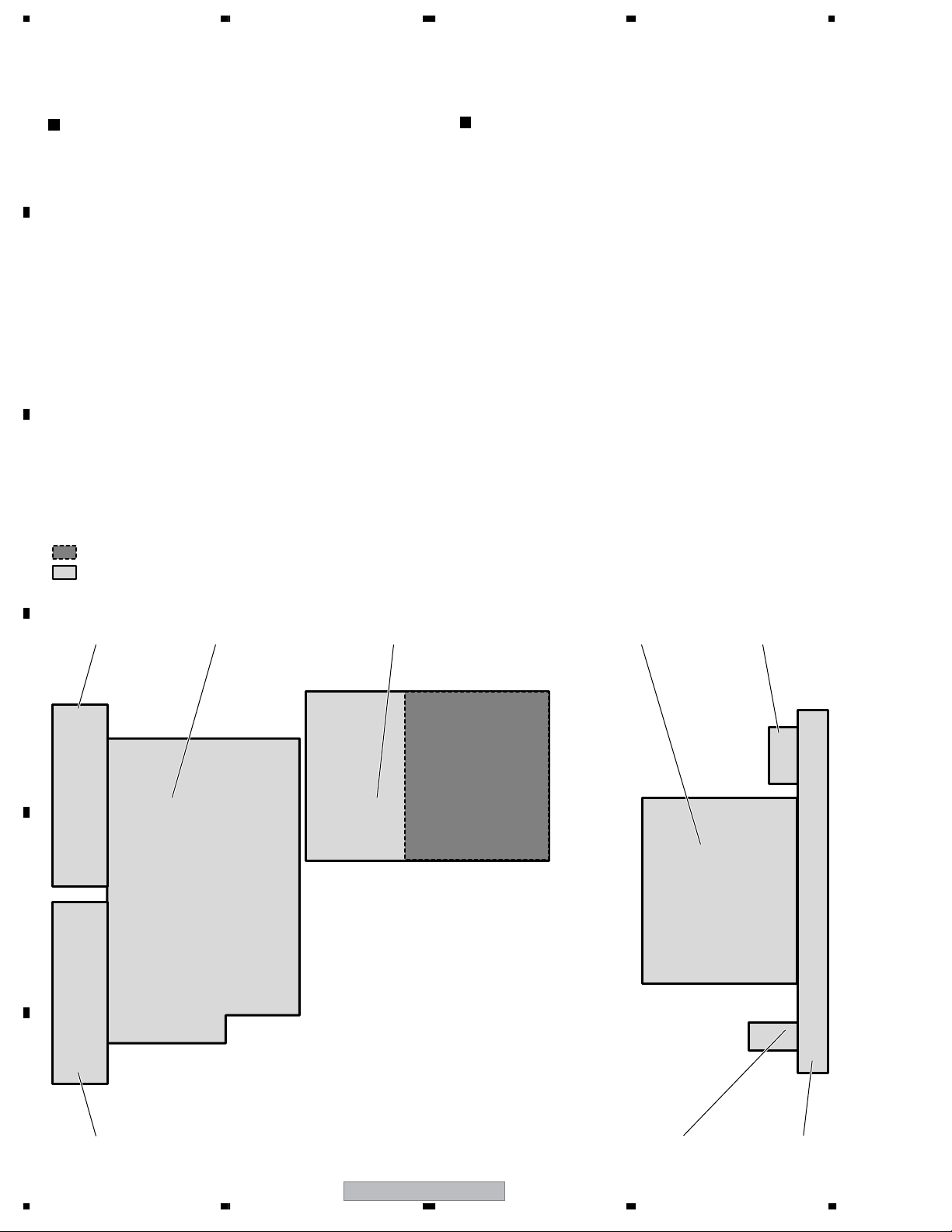
A
Charged Section
The places where the commercial AC power is used without
passing through the power supply transformer.
If the places are touched, there is a risk of electric shock. In
addition, the measuring equipment can be damaged if it is
connected to the GND of the charged section and the GND of the
non-charged section while connecting the set directly to the
commercial AC power supply. Therefore, be sure to connect the
set via an insulated transformer and supply the current.
B
1. Power Cord
2. AC Inlet
3. Power Switch (S1)
4. Fuse (In the POWER SUPPLY Unit)
5. STB Transformer and Converter Transformer
(In the POWER SUPPLY Unit)
6. Other primary side of the POWER SUPPLY Unit
C
: Part is Charged Section.
: Part is the High Voltage Generating Points
other than the Charged Section.
High Voltage Generating Point
The places where voltage is 100V or more except for the charged
places described above. If the places are touched, there is a risk of
electric shock.
If the procedures described in “7.1.4 POWER ON/OFF
FUNCTION FOR THE LARGE POWER SIGNAL SYSTEM”
are performed before the power is turned off, the voltage will be
discharged in about 30 seconds.
1. POWER SUPPLY Unit.....................................................(205V)
2. 42 X DRIVE Assy .......................................... (–180V to 205V)
3. 42 Y DRIVE Assy .......................................................... (500V)
4. 42 SCAN A Assy ............................................................ (500V)
5. 42 SCAN B Assy ............................................................(500V)
6. SUS CLAMP 1 Assy .......................................(–180V to 205V)
7. SUS CLAMP 2 Assy .......................................(–180V to 205V)
42 SCAN B Assy
D
E
42 Y DRIVE Assy 42 X DRIVE Assy SUS CLAMP 1 AssyPOWER SUPPLY Unit
F
42 SCAN A Assy SUS CLAMP 2 Assy PLATE X (FT)
Fig.1 Charged Section and High Voltage Generating Point (Rear View)
4
1234
PDP-425CMX
Page 5
5678
[Important Check Points for Good Servicing]
In this manual, procedures that must be performed during repairs are marked with the below symbol.
Please be sure to confirm and follow these procedures.
1. Product safety
Please conform to product regulations (such as safety and radiation regulations), and maintain a safe servicing environment by
following the safety instructions described in this manual.
1 Use specified parts for repair.
Use genuine parts. Be sure to use important parts for safety.
2 Do not perform modifications without proper instructions.
Please follow the specified safety methods when modification(addition/change of parts) is required due to interferences such as
radio/TV interference and foreign noise.
3 Make sure the soldering of repaired locations is properly performed.
When you solder while repairing, please be sure that there are no cold solder and other debris.
Soldering should be finished with the proper quantity. (Refer to the example)
4 Make sure the screws are tightly fastened.
Please be sure that all screws are fastened, and that there are no loose screws.
5 Make sure each connectors are correctly inserted.
Please be sure that all connectors are inserted, and that there are no imperfect insertion.
6 Make sure the wiring cables are set to their original state.
Please replace the wiring and cables to the original state after repairs.
In addition, be sure that there are no pinched wires, etc.
7 Make sure screws and soldering scraps do not remain inside the product.
Please check that neither solder debris nor screws remain inside the product.
8 There should be no semi-broken wires, scratches, melting, etc. on the coating of the power cord.
Damaged power cords may lead to fire accidents, so please be sure that there are no damages.
If you find a damaged power cord, please exchange it with a suitable one.
9 There should be no spark traces or similar marks on the power plug.
When spark traces or similar marks are found on the power supply plug, please check the connection and advise on secure
connections and suitable usage. Please exchange the power cord if necessary.
0 Safe environment should be secured during servicing.
When you perform repairs, please pay attention to static electricity, furniture, household articles, etc. in order to prevent injuries.
Please pay attention to your surroundings and repair safely.
A
B
C
D
2. Adjustments
To keep the original performance of the products, optimum adjustments and confirmation of characteristics within specification.
Adjustments should be performed in accordance with the procedures/instructions described in this manual.
3. Lubricants, Glues, and Replacement parts
Use grease and adhesives that are equal to the specified substance.
Make sure the proper amount is applied.
4. Cleaning
For parts that require cleaning, such as optical pickups, tape deck heads, lenses and mirrors used in projection monitors, proper
cleaning should be performed to restore their performances.
5. Shipping mode and Shipping screws
To protect products from damages or failures during transit, the shipping mode should be set or the shipping screws should be
installed before shipment. Please be sure to follow this method especially if it is specified in this manual.
56
PDP-425CMX
E
F
5
7
8
Page 6

1234
CONTENTS
1. SPECIFICATIONS ............................................................................................................................................ 7
2. EXPLODED VIEWS AND PARTS LIST .......................................................................................................... 10
A
B
C
D
2.1 PACKING SECTION ................................................................................................................................10
2.2 FRONT and REAR SECTION.................................................................................................................. 12
2.3 TERMINAL SECTION .............................................................................................................................. 14
2.4 MULTIBASE SECTION ............................................................................................................................ 16
2.5 FRAME SECTION.................................................................................................................................... 18
2.6 DRIVE SECTION ..................................................................................................................................... 20
2.7 CHASSIS SECTION ................................................................................................................................22
3. BLOCK DIAGRAM AND SCHEMATIC DIAGRAM..........................................................................................24
3.1 OVERALL CONNECTION DIAGRAM (1/2) ............................................................................................. 24
3.2 OVERALL CONNECTION DIAGRAM (2/2) ............................................................................................. 26
3.3 OVERALL BLOCK DIAGRAM (1/2) ......................................................................................................... 28
3.4 OVERALL BLOCK DIAGRAM (2/2) ......................................................................................................... 30
3.5 MAIN ASSY BLOCK DIAGRAM............................................................................................................... 32
3.6 COMMON SLOT ASSY ...........................................................................................................................34
3.7 KEY, LED, SENB, SENC and SEND ASSYS........................................................................................... 35
3.8 AUDIO and SUS COMM IF ASSYS......................................................................................................... 36
3.9 POWER BLOCK DIAGRAM..................................................................................................................... 38
3.10 CONNECTOR PIN DESCRIPTION .......................................................................................................40
5. PCB PARTS LIST ........................................................................................................................................... 56
6. ADJUSTMENT ............................................................................................................................................... 69
6.1 ADJUSTMENT REQUIRED WHEN THE SET IS REPAIRED OR REPLACED....................................... 69
6.2 ADJUSTMENT......................................................................................................................................... 70
6.3 SERVICE MENU LIST ............................................................................................................................. 73
6.4 SERVICE MENU...................................................................................................................................... 74
6.5 FACTORY MODE..................................................................................................................................... 76
6.6 RS-232C C0MMAND ............................................................................................................................... 87
6.7 METHOD FOR REPLACING THE SERVICE PANEL ASSY.................................................................. 115
7. GENERAL INFORMATION........................................................................................................................... 121
7.1 DIAGNOSIS ........................................................................................................................................... 121
7.1.1 PCB LOCATION ..............................................................................................................................121
7.1.2 DIAGNOSIS OF SHUTDOWN/POWER-DOWN INDICATED BY LEDS.......................................... 122
7.1.3 TROUBLESHOOTING..................................................................................................................... 128
7.1.4 POWER ON/OFF FUNCTION FOR THE LARGE POWER SIGNAL SYSTEM............................... 157
7.1.5 BACKUP WHEN THE MAIN UNIT IS ADJUSTED ..........................................................................158
7.1.6 HOW TO CLEAR HISTORY DATA ................................................................................................... 160
7.1.7 FAN CONTROL ...............................................................................................................................162
7.1.8 POWER ON SEQUENCE................................................................................................................ 163
7.1.9 DISASSEMBLY................................................................................................................................ 164
7.2 IC ........................................................................................................................................................... 170
8. PANEL FACILITIES ...................................................................................................................................... 180
E
F
6
1234
PDP-425CMX
Page 7

5678
1. SPECIFICATIONS
General
Light emission panel ................ 42V type AC Plasma Panel
92.16 cm (W) x 51.53 cm (H) x 105.59 cm (diagonal)
Number of pixels .............................................. 1024 x 768
Power supply (for 425CMX)....... AC 100 - 120 V, 50/60 Hz
(for 42MXE10)...... AC 100 - 240 V, 50/60 Hz
Rated current (for 425CMX)........................... 3.0 A - 2.5 A
(for 42MXE10)......................... 3.0 A - 1.3 A
Standby power consumption (for 425CMX).............. 1.2 W
(for 42MXE10)............ 1.5 W
External dimensions
............................... 1022 mm (W) x 610 mm (H) x 98 mm
(D: Not including handles)
40-1/4 in. (W) x 24 in. (H) x 3-7/8 in.
(D: Not including handles)
(including display stand)
....................... 1218 mm (W) x 737 mm (H) x 300 mm (D)
47-31/32 in. (W) x 29-1/32 in. (H) x 11-13/16 in. (D)
Weight .......................................................30.5 kg (67 lbs.)
(including display stand)............................31.1 kg (69 lbs.)
Input/output
Video
INPUT1
Input Mini D-sub 15 pin (socket connector)
RGB signal (G ON SYNC compatible)
RGB ... 0.7 Vp-p/75 Ω/no sync.
HD/VS, VD ... TTL level
/positive and negative polarity
/2.2 kΩ
G ON SYNC
... 1 Vp-p/75 /negative sync.
*Compatible with Microsoft “ Plug & Play”
(VESA DDC1/2B)
Output Mini D-sub 15 pin (socket connector)
75Ω /with buffer
INPUT2
Input DVI-D 24-pin connector
Digital RGB signal (DVI compliant TMDS
signal)
*Compatible with Microsoft “ Plug & Play”
(VESA DDC 2B)
Audio
Input AUDIO INPUT (for INPUT1)
Stereo mini jack
L/R ... 500 mVrms/more than 10 kΩ
AUDIO INPUT (for INPUT2)
Stereo mini jack
L/R ... 500 mVrms/more than 10 kΩ
Output AUDIO OUTPUT
Stereo mini jack
L/R ... 500 mVrms (max)/less than 5 kΩ
SPEAKER
L/R ... 6 Ω/8 W +8 W (at 6Ω )
Control
RS-232C... D-sub 9 pin (pin connector)
COMBINATION IN/OUT
... Mini DIN 6 pin (x2)
Accessories
Power cord (for 425CMX)..................................................1
Remote control unit ......................................................... 1
Remote control unit holder .............................................. 1
AA (R6) batteries.............................................................. 2
Cleaning cloth (for screen) ............................................... 1
Speed clamps................................................................... 5
Display stands .................................................................. 2
Washers ........................................................................... 2
Hex hole bolts (M8X40).................................................... 2
Ferrite cores (for power cord) .......................................... 2
Ferrite cores (for audio cables)......................................... 3
Cable ties ......................................................................... 2
Operating Instructions (for 425CMX)................................ 1
Operating Instructions (CD-ROM) (for 42MXE10).............1
Start up Guide (for 42MXE10) ......................................... 1
Warranty(for 425CMX)..................................................... 1
A
B
C
D
¶ Due to improvements, specifications and design are subject to
change without notice.
PDP-425CMX
56
E
F
7
7
8
Page 8

1234
A
1 Power cord
(ADG1215)
2 Remote control unit
(AXD1528)
7 Ferrite cores (x 3) (for audio cables)
(CTX1054)
B
3 AA (R6) batteries (x 2)
C
4 Cleaning cloth (for screen)
(AED1285)
5 Speed clamps (x 5)
(AEC2051)
D
8 Display stands (x 2)
(AMR3545)
9 Washers (x 2)
(WB80FTC)
0 Hex hole bolts (x 2)
(SMZ80H400FTC)
- Remote control unit holder
(AMR3268)
6 Ferrite cores (x 2) (for power cord)
(ATX1031)
E
F
8
1234
Use as a holder for the
remote control unit.
When attaching to the
rear of the main unit,
be careful not to cover
the vents.
= Cable ties (x 2)
(AEC-093)
• These Operating Instructions
• Warranty
PDP-425CMX
Page 9

5678
A
B
C
D
E
56
PDP-425CMX
F
9
7
8
Page 10

1234
2. EXPLODED VIEWS AND PARTS LIST
NOTES:
Parts marked by "NSP" are generally unavailable because they are not in our Master Spare Parts List.
The mark found on some component parts indicates the importance of the safety factor of the part.
A
Therefore, when replacing, be sure to use parts of identical designation.
Screws adjacent to mark on product are used for disassembly.
For the applying amount of lubricants or glue, follow the instructions in this manual.
(In the case of no amount instructions, apply as you think it appropriate.)
2.1 PACKING SECTION
B
12
14×2
13×2
C
6×5
5×2
24
10×2
11
PDP-425CMX
23
only
22
25
×3
9
×2
35
33
7, 15-17, 19,
20, 37-39
D
21
4
E
8
2, 3
PDP-425CMX
only
29
1
32
31
30
36
18
(Except
PDP-42MXE10/YVXK5)
27
28
26
F
34
10
1234
PDP-425CMX
Page 11
>
5678
(1) PACKING SECTION PARTS LIST
No. Description Part No.
Mark
1Power Cord See Contrast table (2)
2 Remote Control Unit
3 Battery Cover
NSP 4 Dry Cell Battery (R6P, AA) VEM1031
5 Cable tie AEC-093
AXD1528
AZN2462
No. Description Part No.
Mark
19 Caution Sheet ARM1245
20 Caution Sheet See Contrast table (2)
NSP 21 Warranty Card See Contrast table (2)
NSP 22 Warranty Card See Contrast table (2)
NSP 23 Polyethylene Bag See Contrast table (2)
A
6 Speed clamp AEC2051
7 Cleaning Cloth AED1285
8 Remote Control Holder AMR3268
9 Display Stand AMR3545
10 Ferrite Core (for power cord) ATX1031
11 Ferrite Core (for audio cables) CTX1054
12 Screws Set AXX1071
13 Hex hole bolt SMZ80H400FTC
14 Washer WB80FTC
15 Operating Instructions See Contrast table (2)
(English, French, Japanese)
16 Operating Instructions See Contrast table (2)
(English)
17 Operating Instructions See Contrast table (2)
(7L)(CD-ROM)
18 Caution Sheet See Contrast table (2)
24 Catalogue Bag AHG1310
25 Catalogue Bag S AHG1338
26 Pad BL (FT) See Contrast table (2)
27 Pad BR (FT) See Contrast table (2)
28 Pad BC (FT) See Contrast table (2)
29 Pad TL (FT) See Contrast table (2)
30 Pad TR (FT) See Contrast table (2)
31 Accessory Case See Contrast table (2)
32 Power Cord Case See Contrast table (2)
33 Reinforce Pad (FT) See Contrast table (2)
34 Carton (42FT) See Contrast table (2)
35 Upper Carton See Contrast table (2)
36 Mirror Mat See Contrast table (2)
37 Plasma Caution Sheet See Contrast table (2)
38 Image Caution Sheet See Contrast table (2)
39 Image Stick Caution Sheet See Contrast table (2)
(2) CONTRAST TABLE
PDP-425CMX/LUC5, PDP-42MXE10/LDFK5 and YVXK5 are constructed the same except for the following:
Mark No. Symbol and Description
>
1Power Cord ADG1215 Not used Not used
15 Operating Instructions (English, French, Japanese) ARD1070 Not used Not used
16 Operating Instructions (English) Not used ARE1419 ARE1419
17 Operating Instructions (7L)(CD-ROM) Not used ARU1001 ARU1001
18 Caution Sheet ARM1201 ARM1201 Not used
PDP-425CMX
/LUC5
PDP-42MXE10
/LDFK5
PDP-42MXE10
/YVXK5
B
C
D
20 Caution Sheet Not used Not used ARM1279
NSP 21 Warranty Card ARY1146 Not used Not used
NSP 21 Warranty Card (EU) Not used ARY1149 ARY1149
NSP 22 Warranty Card ARY1146 Not used Not used
NSP 23 Polyethylene Bag AHG-195 Not used Not used
26 Pad BL (FT) AHA2495 AHA2495 AHA2528
27 Pad BR (FT) AHA2496 AHA2496 AHA2529
28 Pad BC (FT) AHA2497 AHA2497 AHA2530
29 Pad TL (FT) AHA2522 AHA2522 AHA2531
30 Pad TR (FT) AHA2523 AHA2523 AHA2532
31 Accessory Case AHC1072 AHC1072 AHC1078
32 Power Cord Case AHC1077 AHC1077 AHC1081
33 Reinforce Pad AHC1079 AHC1079 AHC1080
34 Carton (42FT) AHD3417 AHD3417 AHD3458
35 Upper Carton AHD3418 AHD3455 AHD3461
36 Mirror Mat AHG1284 AHG1284 AHG1327
37 Plasma Caution Sheet ARM1147 Not used Not used
38 Image Caution Sheet ARM1220 Not used Not used
39 Image Stick Caution Sheet ARM1299 Not used Not used
PDP-425CMX
56
7
8
E
F
11
Page 12

1234
2.2 FRONT and REAR SECTION
A
314
33
3
B
C
D
7
21
5
11
PDP-425CMX
only
22
3
3
1613
1
12
22 22 22 22
21
15
21 21
3
22
3
3
3 3
224 2
5
6
22
18
22
22
E
8
22
22
F
12
1234
22
22
22
9 10
22
22
22
22 1922
22
22
22
22
22
PDP-425CMX
22
22
22
22
22
22
22
22
17
Page 13

>
5678
(1) FRONT and REAR SECTIONS PARTS LIST
No. Description Part No.
Mark
1 KEY Assy AWW1108
2 LED2 Assy AWW1109
NSP 3 Panel Holder (FT) ANG2840
4 PCB Spacer AEC1947
5 Inner Grip Assy AMR3434
NSP 6 Name Label See Contrast table (2)
7 Serial Sheet AAX3143
8Terminal Label MAIN A (CMX) See Contrast table (2)
9Terminal Label MAIN B (CMX) See Contrast table (2)
10 Terminal Label MAIN C (CMX) See Contrast table (2)
A
11 Caution Label (CMX) See Contrast table (2)
12 Caution Label See Contrast table (2)
13 Front Case Assy (425CMX) AMB2885
14 Filter (FT) AMR3510
15 Control Button (CMX) AAC1559
16 Pioneer Badge AAM1101
17 Control Cover (CMX) AMR3512
18 Rear Case ANE1650
19 Bottom Cover (CMX) ANG2860
20 • • • • •
21 Screw ABZ30P100FTB
22 Screw AMZ30P060FTB
(2) CONTRAST TABLE
PDP-425CMX/LUC5, PDP-42MXE10/LDFK5 and YVXK5 are constructed the same except for the following:
Mark No. Symbol and Description
NSP 6 Name Label (CMX) AAL2726 Not used Not used
NSP 6 Name Label (MXE) Not used AAL2734 AAL2746
8Terminal Label MAIN A (CMX) AAX3250 AAX3250 AAX3292
9Terminal Label MAIN B (CMX) AAX3251 AAX3251 AAX3293
10 Terminal Label MAIN C (CMX) AAX3252 AAX3252 AAX3294
PDP-425CMX
/LUC5
PDP-42MXE10
/LDFK5
PDP-42MXE10
/YVXK5
B
C
D
11 Caution Label (CMX) AAX3253 Not used Not used
12 Caution Label M AAX3304 AAX3304 Not used
12 Caution Label Not used Not used AAX3295
PDP-425CMX
56
7
8
E
F
13
Page 14
1234
2.3 TERMINAL SECTION
A
Filter styling
28
27
5, 28
43
31
5
32
29
36
32
45
4
45
44
8
16
5, 28
5, 28
11
28
5, 28
18
4040
43
14
43
5, 28
383838
3737
91
3423
43
17
43
43
B
12
5, 28
C
313
42
D
35
43
43
33
24
43
29
26
42
43
29
2
33
43
29
43
5, 28
28
32
39
10
43
30
E
F
19
15
30
4321 43
5, 28
43
25
14
1234
30
43
PDP-425CMX
20
43 43
42 42
38
41 41
227 6
43
Page 15

5678
TERMINAL SECTION PARTS LIST
No. Description Part No.
Mark
1AUDIO Assy AWW1105
2 COMMSLOT Assy AWW1106
3 COMMSLOT IF Assy AWW1107
4 SENC Assy AWW1103
5 Filter CTX1054
6Power Switch (S1) ASG1094
7AC Inlet (CN1) AKP1296
8 1P Wire GND (J209) ADX3242
9 9P Housing Wire (J220) ADX3262
10 7P Housing Wire (J201) ADX3263
>
>
A
11 13P Housing Wire (J202) ADX3264
12 8P Housing Wire (J204) ADX3265
13 40P Housing Wire (J205) ADX3268
14 6P Housing Wire (J222) ADX3270
15 8P Housing Wire (J221) ADX3283
16 Housing Wire (J216) ADX3284
17 Housing Wire (J210) ADX3285
18 13P Housing Wire (J218) ADX3286
19 COMM Bracket (CMX) ANG2857
20 Terminal Panel AC (CMX) ANG2863
21 Terminal Panel COMM (CMX) ANG2874
22 AC Bracket (CMX) Assy ANG2901
NSP 23 Audio Heatsink ANH1648
24 Slot Spring T94 ABK1034
25 Slot Spring B92 ABK1035
26 COMM I/F Bracket (CMX) ANG2859
27 Inlet Cover (XM4) ANG2899
28 Nyron Binder AEC-093
29 Wire Saddle AEC1745
30 Mini Clamp AEC1805
31 Harness Lifter 18 AEC1980
32 Omega Lock AEC2084
33 COMM Rail (CMX) AMR3486
34 Thermal Sheet AUDIO AMR3507
35 Gasket ANK1823
B
C
D
36 Gasket ANK1827
37 Gasket ANK1828
38 Gasket ANK1829
39 Gasket ANK1830
40 Gasket ANK1831
41 Screw ABA1342
42 Screw ABZ30P100FTB
43 Screw AMZ30P060FTB
44 Screw BMP40P080FBN
45 PCB Spacer AEC1941
56
PDP-425CMX
E
F
15
7
8
Page 16

1234
2.4 MULTIBASE SECTION
A
19
19
19
7
3
21
17
23
23
16
23
5
21
3
3
21
9
2 12
24 24
18
13
14141414
4
21
13
13
13
24
6
23
13
17
23
23
21
15
B
1414
C
D
21
14
1
21
21
21 21
22 22
E
F
22
16
1234
222222
PDP-425CMX
11
10
8
Page 17

5678
(1) MULTI BASE SECTION PARTS LIST
No. Description Part No.
Mark
1 MAIN Assy See Contrast table (2)
2 VSIF Assy See Contrast table (2)
3 Flexible Cable (J219) ADD1342
4 20P Housing Wire (J215) ADX3273
5 20P Housing Wire (J217) ADX3274
A
6LVDS Cable (J223)
7 Multi Base (CMX) ANA1901
8
11 Slot Panel 262 (N) ANG2610
12 VIDEO I/F Bracket ANG2858
13 Wire Saddle AEC1745
14 Wire Saddle AEC1797
15 PCB Support AEC1958
16 Rivet AMR1066
17 VIDEO Guide Rail AMR3485
18 VIDEO I/F Sheet AMR3495
19 PWB Sleeve AMR3518
20 • • • • •
21 Screw AMZ30P060FTB
22 Hex Head Screw BBA1051
23 Screw PMB30P100FNI
24 Screw VBB30P080FNI
Te r minal Panel MAIN (CMX) Assy
9 Slot Spring T130 ABK1032
10 Slot Spring B126 ABK1033
ADX3276 (or ADX3289)
ANG2871
B
C
(2) CONTRAST TABLE
PDP-425CMX/LUC5, PDP-42MXE10/LDFK5 and YVXK5 are constructed the same except for the following:
Mark No. Symbol and Description
1 MAIN Assy AWW1100 AWW1112 AWW1112
2 VSIF Assy AWW1101 AWW1113 AWW1113
PDP-425CMX
/LUC5
PDP-42MXE10
/LDFK5
PDP-42MXE10
/YVXK5
D
E
F
56
PDP-425CMX
17
7
8
Page 18

1234
2.5 FRAME SECTION
A
20
3
B
31 31
C
31
31
15
30
20
17 24
31
29
31
30
26
13
17
22
21
14
20
17
23
29
7
31
31
31
30
26
31
31
31
22
21
20
1
8
15
30
17
17
D
28
E
31
17
31
17
29 29
28
31
12
31
17
18
5, 16
31
18
19
19
19
19
17
28
17
19
6
31
19
28
19
31
F
28
10 11
18
1234
282828
3131
PDP-425CMX
31
25
9
25
31
Page 19

5678
FRAME SECTION PARTS LIST
No. Description Part No.
Mark
1 SENB Assy AWW1102
2• • • • •
3 SEND Assy AWW1104
4• • • • •
5 Filter CTX1054
6 3P Housing Wire (J206) ADX3266
7 4P Housing Wire (J207) ADX3267
8Front Chassis U (FT) ANA1907
9Front Chassis R (FT) ANA1918
10 Front Chassis LA ANA1926
A
11 Front Chassis LB (FT) ANA1928
12 Front Chassis B (CMX) ANA1933
13 Sub Frame L Assy (CMX) ANG2875
14 Sub Frame R Assy (CMX) ANG2876
15 Fan Angle (FT) ANG2909
16 Nyron Binder AEC-093
17 Wire Saddle AEC1745
18 Wire Saddle AEC1751
19 Mini Clamp AEC1805
20 PCB Spacer AEC1941
21 Cushion A AED1293
22 Cushion B AED1294
23 Duct Sheet L (FT) AMR3515
24 Duct Sheet R (FT) AMR3532
25 Gasket ANK1823
26 Fan Motor 80 x 25L AXM1054
27 • • • • •
28 Screw AMZ30P060FTB
29 Screw PMB50P120FTC
30 Screw PPZ50P100FTB
31 Screw VBB30P080FNI
B
C
D
56
PDP-425CMX
E
F
19
7
8
Page 20

1234
2.6 DRIVE SECTION
A
9
222222
23
B
C
7
23
14 4
23
23
13
22
23
23
23
1920
6, 16
1018 18
D
E
F
22
18
18
18
12
23
2
18
23
11
181818
23
18
18
23
5
3
23
23
222222222222
23
8
1
22
20
PDP-425CMX
1234
Page 21

5678
DRIVE SECTION PARTS LIST
No. Description Part No.
Mark
1 SUS CLAMP 1 Assy AWW1022
2 SUS CLAMP 2 Assy AWW1023
3 42 X DRIVE Assy AWW1067
4 42 Y DRIVE Assy AWV2251
5POWER SUPPLY Unit AXY1127
6Ferrite Core ATX1039
7 4P Housing Wire (J101) ADX3192
8 6P Housing Wire (J102) ADX3193
9 3P Housing Wire (J103) ADX3194
10 8P Housing Wire (J105) ADX3196
>
A
11 14P Housing Wire (J106) ADX3292
12 5P Housing Wire (J108) ADX3199
13 9P Housing Wire (J104) ADX3278
14 6P Housing Wire (J107) ADX3280
15 • • • • •
16 Nyron Binder AEC-093
17 • • • • •
18 Locking Wire Saddle AEC1992
19 HS Sheet S (FT) AMR3519
20 HS Sheet L (FT) AMR3520
21 • • • • •
22 Screw PMB30P060FTC
23 Screw VBB30P080FNI
B
C
D
56
PDP-425CMX
E
F
21
7
8
Page 22

1234
2.7 CHASSIS SECTION
A
Note : The parts of encircled number denote measuring component of PDP Service Assy.
18
15
16
20
16
19
20
20
16
16
16
16
15
14
10
16
9
14
14
B
17 8
C
14
14
11
16
16
16
16
141414
13
13
16
7
5
16
14
13
16
17
16
16
13
13
16
12
D
6666
1
16
E
3
2
F
4 4 4 4
16
1616
16
22
PDP-425CMX
1234
Page 23

5678
(1) PANEL CHASSIS SECTION PARTS LIST
No. Description Part No.
Mark
NSP 1 Panel Chassis (FT) Assy See Contrast table (2)
2 42 SCAN A Assy AWW1071
3 42 SCAN B Assy AWW1072
4 42 ADDRESS Assy AWV2253
5 MD DIGITAL Assy AWV2254
No. Description Part No.
Mark
11 Flexible Cable (J120) ADD1333
12 Flexible Cable (J211) ADD1334
13 Wire Saddle AEC1745
14 Flat Clamp AEC1879
15 PCB Support AEC1938
A
6Ferrite Core ATX1048
7 Flexible Cable (J109) ADD1329
8 Flexible Cable (J110) ADD1330
9 Flexible Cable (J117) ADD1331
10 Flexible Cable (J119) ADD1332
16 PCB Spacer AEC1941
17 Drive Silicone Sheet AEH1095
18 Power Sheet (FT) AMR3521
19 Y Drive Protect Sheet (FT) AMR3525
20 Harness Lifter 18 AEC1980
(2) CONTRAST TABLE
PDP-425CMX/LUC5, PDP-42MXE10/LDFK5 and YVXK5 are constructed the same except for the following:
Mark No. Symbol and Description
NSP 1 Panel Chassis (FT) Assy AWU1136 AWU1136 AWU1151
PDP-425CMX
/LUC5
PDP-42MXE10
/LDFK5
PDP-42MXE10
/YVXK5
2.8 PDP SERVICE ASSY
PDP SERVICE ASSY PARTS LIST
No. Description Part No.
No. Description Part No.
Mark
PDP Service Assy 42H6D1 AWU1160
NSP Panel Chassis (FT) Assy AWU1136
Wire Saddle AEC1745 x5
Flat Clamp AEC1879 x9
PCB Support AEC1938 x2
PCB Spacer AEC1941 x22
Harness Lifter 18 AEC1980 x2
Power Sheet (FT) AMR3521
Y Drive Protect Sheet (FT) AMR3525
Caution Label AAX3031 x2
Screw PMB50P150FTC x4
Mark
Accessories
Wire Saddle AEC1745 x13
PCB Spacer AEC1941 x4
Harness Lifter 18 AEC1980
Locking Wire Saddle AEC1992 x11
Vinyl Bag S AHG1338
Sheet (FT) AMR3530 x2
Packing parts
Pad 42 Single (T-L) AHA2550
Pad 42 Single (T-R) AHA2551
Pad 42 Single (B-L) AHA2552
Pad 42 Single (B-R) AHA2553
Upper Carton (42 Single) AHD3480
B
C
D
E
Under Carton (42 Single) AHD3481
Polyethylene Bag AHG1381
Packing Sheet AHG1386
Tr ay (FT) AHX1158
Cup Spacer (15) ANG2936 x4
PDP-425CMX
56
F
23
7
8
Page 24

1234
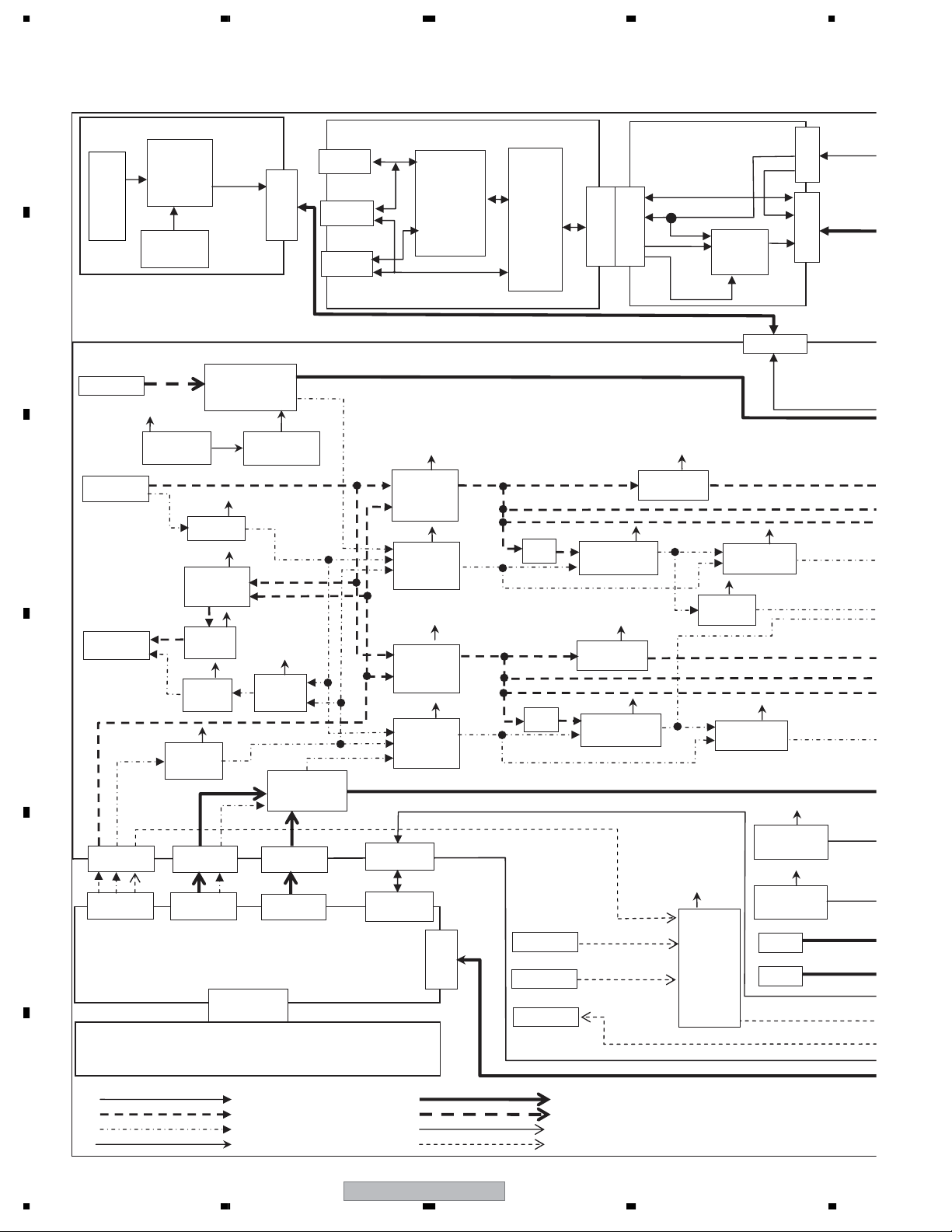
3. BLOCK DIAGRAM AND SCHEMATIC DIAGRAM
3.1 OVERALL CONNECTION DIAGRAM (1/2)
A
÷
When ordering service parts, be sure to refer to "EXPLODED VIEWS and PARTS
LIST" or "PCB PARTS LIST".
÷
The > mark found on some component parts indicates the importance of the safety
factor of the part. Therefore, when replacing, be sure to use parts of identical
designation.
ADX3268
123
1
FAN-CTL
2
GND
3
F-ALM
FB
FAN-CTL
1
GND
103
103
2
3
1
2
3
4
5
6
7
8
1
2
3
4
5
6
7
8
9
...
...
F-ALM
A+12
A.GND
A+6
A+6
A.GND
A.GND
NC
NC
AU-L
GND
AU-R
GND
SP_ALM
GND
MUTE
SCL7
SDA7
CN2303
AKP1252
.
.
123
124
232425
123
124
232425
FA
CN9008
AKM1279
CN9001
AKM1280
125
125
CN4004→CN5301
26.→25.GPC4
27.→24.GPC2
28.→23.GPC5
29.→22.GND
30.→21.VYOBI1
31.→10.VYOBI2
32.→19.GND
33.→18.DSUBSW_DET
34.→17.G4G
35.→16.FNC0
36.→15.IR
37.→14.SLOT_ST2
38.→13.FNC1
39.→12.S_DIN_SEL
40.→11.SLOT_ST1
41.→10.IN4_DET
42. →9.GND
43. →8.SDA_VS
44. →7.SCL_VS
45. →6.SDA5
46. →5.SCL5
47. →4.GND
48. →3.VCC_DOWN1
49. →2.PNP_WR
50. →1.NC
CN9004
AKM1274
CN9003
AKM1274
PV
AU
CN5010
AKM1343
246..
135..
.
363840
.
353739
CN9010
AKM1342
CN5001, CN4005
1.GND
3.Y(G)ON_SYNC
5.GND
7.B(B-Y)
9.GND
11.R(R-Y)
13.GND
15.HD_SA
17.GND
19.VD_SA
151719
.
161820
.
ADX3274
151719
.
161820
.
CN4005 AKM1343
CN4003→CN6302
1.→50.GA4
2.→49.GND
3.→48.GB4
4.→47.GND
5.→46.GA3
6.→45.GND
7.→44.GB5
8.→43.GND
9.→42.GA2
10.→41.GND
11.→40.GB6
12.→39.GND
13.→38.GA1
14.→37.GND
15.→39.GB7
16.→35.GND
17.→34.GA0
18.→33.GND
19.→32.BB0
20.→31.GND
21.→30.RA7
22.→29.GND
23.→28.BB1
24.→27.GND
25.→26.RA6
SCL5
TM
2.NC
4.GND
6.MC
8.GND
10.NC
12.GND
14.AUDIO_R
16.GND
18.AUDIO_L
20.GND
135..
246..
135..
246..
CN4006
AKP1251
26.→25.GND
27.→24.BB2
28.→23.GND
29.→22.RA5
30.→21.GND
31.→10.BB3
32.→19.GND
33.→18.RA4
34.→17.GND
35.→16.BB4
36.→15.GND
37.→14.RA3
38.→13.GND
39.→12.BB5
40.→11.GND
41.→10.RA2
42.→ 9.GND
43. →8.BB6
44. →7.GND
45. →6.RA1
46. →5.GND
47. →4.BB7
48. →3.GND
49. →2.RA0
50. →1.GND
4
1234567
GND
VDD+3.3V
CN9501
AKM1275
SDA5
M+7V
PM
D.GND
NCNCNCNCNC
CN9006
AKM1278
MAIN ASSY
PDP-425CMX
AWW1100
CN5301 AKM1345 CN6302 AKM1345
123..
CN4004 AKM1345 CN4003 AKM1345 CN4002 AKM1345
196
CN4002→CN6301
1.→50.VD
2.→49.HD
3.→48.DE
4.→47.CLK
5.→46.GND
6.→45.RB0
7.→44.GND
8.→43.BA7
9.→42.GND
10.→41.RB1
11.→40.GND
12.→39.BA6
13.→38.GND
14.→37.RB2
15.→39.GND
16.→35.BA5
17.→34.GND
18.→33.RB3
19.→32.GND
20.→31.BA4
21.→30.GND
22.→29.RB4
23.→28.GND
24.→27.BA3
25.→26.GND
.
484950
ADD1342 ADD1342- ADD1342
195
484950
194
949596
.
...
...
CN4006
Card edge
connector
26.→25.RB5
27.→24.GND
28.→23.BA2
29.→22.GND
30.→21.RB6
31.→10.GND
32.→19.BA1
33.→18.GND
34.→17.RB7
35.→16.GND
36.→15.BA0
37.→14.GND
38.→13.GB0
39.→12.GND
40.→11.GB1
41.→10.GND
42.→ 9.GB1
43.→ 8.GND
44.→ 7.GA6
45.→ 6.GND
46.→ 5.GB2.
47. 4.GND
48.→ 3.GA5
49.→ 2.GND
50.→ 1.GB3
167
166
123..
165
656667
1.GND
3.G
5.B
7.R
9.HD_SA
11.VD_SA
13.AUDIO_L
15.AUDIO_R
17.SLOT_ST1
19.FNC1
21.V+3.3V
23.NC
25.HD_DET
27.VD
29.HD
31.GND
33.RB1
35.RB3
37.RB5
39.RB7
41.GND
43.GB1
45.GB3
47.GB5
49.GB7
53.GND
55.BB1
57.BB3
59.BB5
61.BB7
65.GND
67.KEY
69.TXD_CARD
71.INT_EXT
73.EMGREQ1_V
75.IC1V_OE
77.NC
79.FNC2
81.SOUND1
83.DSUBR
85.DSUBG
87.SDUBB
89.IN5_HD
91.GPC1
93.GPC5
95.VYOBI2
12345
D+3.3
D+3.3
PN1 PN2
PDP-42MXE10
AWW1112
123..
.
484950
.
154
160
161
162
...
606162
...
2.GND
4.GND
6.GND
8.GND
10.GND
12.GND
14.GND
16.GND
18.S_DIN_SEL
20.FNC0
22.V+3.3V
24.GND
26.GND
28.GND
30.GND
32.RB0
34.RB2
36.RB4
38.RB6
40.GND
42.GB0
44.GB2
46.GB4
48.GB6
52.GND
54.BB0
56.BB2
58.BB4
60.BB6
62.GND
66.GND
68.NC
70.RXD_CARD
72.NC
74.EMGREQ2_V
76.RESETX1
78.SD_SEL
80.FNC3
82.GND
84.GND
86.GND
88.GND
90.SOUSA_X
92.GPC2
94.VYOBI1
96.DSUNSW_DET
FAN(1&2)
AXM1054
"FAN" may be connected
B
to either "FA" or "FB"
CN9010,CN2302
1.VCC_DOWN2
3.NC
5.NC
7.LEDCTL1
C
D
9.LEDCTL2
11.RLS
13.VDDM3.3V
15.VDDM5V
17.4G/5G
19.TXD2
21.PLE_CTL2
23.RXD2
25.PLE_CTL
27.STL_LINK
29.CB_MUTE
31.KEY
33.RXD
35.TXD
37.GND
39.GPC1
CN2301
KM200NA8L
LEDCTL1LEDCTL1
REMIN
1234567
1234567
REMIN
LEDCTL2 LEDCTL2
LED2 ASSY
AWW1109
E
CN2303,Card edge connector
1.NC
2.IRSW
3.IR_COMM_OUT
4.IR_COMM_IN
5.GND
6.GND
7.GND
8.CYOBI3
9.CYOBI2
10.CSL_ST2
11.CSL_ST1
14.GND
15.GND
16.FIRST_RXD
17.GET_UART
18.INT_EXT
19.RXD_CARD
20.TXD_CARD
21.GPC5
F
22.GPC4
23.GPC3
24.GPC2
25.GPC1
FAN(1) FAN(2)
2.V+6.5V
4.CSL_ST1
6.REMIN
8.GND
10.CYOBI3
12.CYOBI2
14.CSL_ST2
16.VDDM3.3V
18.GND
20.VDDM5V
22.GND
24.FIRST_RXD
26.GET_UART
28.INT_EXT
30.RXD_GU
32.TXD_GU
34.GPC5
36.GPC4
38.GPC3
40.GPC2
CN2302
AKM1347
246..
135..
COMM SLOT I/F ASSY
AWW1107
VDDM5V
VDDM3.3V
GND
RLS
GND
8
ADX3283
8
GND
RLS
GND
VDDM5V
CN2101
VDDM3.3V
AKM1294
COMM SLOT
ASSY
AWW1106
101.NC
102.GND
103.GND
104.GND
105.TXD_PDP
106.RXD_PDP
107.KEY_COMM_IN
108.CB_MUTE
109.STL_LINK
110.GND
111.GND
114.V+6.5V
115.V+6.5V
116.GND
117.GND
118.VDDM3.3V
119.VDDM3.3V
120.VDDM5
121.APL_CTL1
122.APL_RXD
123.APL_CTL2
124.APL_TXD
125.SLT_Vrer
ADX3262
AU:SHIELD-WIRE
(1,3pin:shield)
.
363840
.
353739
101
102
123..
101
102
123..
Card edge connector
1.←50.VDDM3.3V
2.→49.NC
3.→48.NC
4.→47.KEY
5.→46.GND
6.→45.GET_UART
7.→44.TXD_CARD
8.→43.FIRST_RXD
9.→42.RXD_CARD
10.→41.INT_EXT
11.→40.GND
12.→39.RESETX1
13.→38.SLOT_ST3
14.→37.SD_SEL
15.→39.SOUND2
16.→35.FNC3
17.→34.FNC2
18.→33.SOUND1
19.→32.GND
20.→31.IN5_VD
21.→30.IN5_HD
22.→29.GND
23.→28.HYOUJI_X
24.→27.GPC3
25.→26.GPC1
D+3.3
D.GND
D.GND
CN9007
AKM1277
484950
123..
152
153
525354
6
1234567
D+2.7
D+2.7
D.GND
CN6301 AKM1345
123..
484950
147
148
149
474849
.
101.GND
103.GND
105.GND
107.GND
109.GND
111.GND
113.GND
115.V+13.5
117.IN4_DET
119.SLOT_ST2
121.NC
123.GND
125.3G4G
127.GND
129.GND
131.GND
133.BA6
135.BA4
137.BA2
139.BA0
141.GND
143.GA6
145.GA4
147.GA2
149.GA0
153.GND
155.RA6
157.RA4
159.RA2
161.RA0
165.GND
167.VSEPSCL
169.NC
171.FIRST_RXD
173.EMGREQ1_S
175.IC1S_OE
177.NC
179.SLOT_ST3
181.SOUND2
183.GND
185.GND
187.GND
189.IN5_VD
191.GPC3
193.NC
195.VYOBI5
NC
D+2.7
D.GND
D.GND
CN9012
AKM1278
CN8502 AD2
1.GND
3.P_ST_B
5.NC
7.NC
9.NC
11.NC
13.NC
15.NC
17.NC
19.GND
.
484950
.
101
102
103
...
123..
D.GND
2.GND
4.MR_ST_B
6.MR_RXD
8.AC_DET_B
10.REQ
12.MR_TXD
14.STB_MUTE
16.VIS
18.FIELD
20.GND
123..
102.GND
104.SCL_VS
106.SDA_VS
108.GND
110.V+12V
112.V+12V
114.V+3.3STB
116.V+13.5
118.IN3_DET
120.IR
122.NC
124.GND
126.IN5_DET
128.DE
130.CLK
132.BA7
134.BA5
136.BA3
138.BA1
140.GND
142.GA7
144.GA5
146.GA3
148.GA1
152.GND
154.RA7
156.RA5
158.RA3
160.RA1
162.GND
166.GND
168.VSEPSDA
170.GET_UART
172.NC
174.EMGREQ2_S
176.NC
178.NC
180.M_CHOICE
182.GND
184.DSUBH
186.DSUBV
188.GND
190.HYOUJI_X
192.GPC4
194.VYOBI4
196.VYOBI6
24
PDP-425CMX
1234
Page 25

5678
SW
CN9011
AKM1274
AD2
CN8502
AKM1343
CN8501 AD1
1.GND
2.GND
3.GND
4.RE+
5.RE-
6.RD+
7.RD-
8.RCLK+
9.RCLK-
10.GND
11.RC+
12.RC-
13.RB+
14.RB-
15.RA+
VIDEO SLOT IF ASSY
PDP-425CMX
AWW1101
16.RA-
17.GND
18.NC
19.NC
20.NC
21.NC
22.NC
23.NC
24.GND
25.MSEL
26.POWER
27.
STB_MUTE
28.RFU
29.STATUS
30.GND
31.GND
123456789
CN4001 AKM1299
PDP-42MXE10
VDDM3
KEY
GND
1
3
5
.
.
.
15
17
19
AD1
CN8501
AKM1339
101112
AWW1113
TEMP-SENSOR1
SENB ASSY
CN1001
AKM1279
TM2
SCL5
GND
VDD+3.3V
SDA5
SCL5
GND
VDD+3.3V
123
4
ADX3267
1
2
3
2
4
6
.
.
.
16
18
20
1
2
3
.
.
.
29
30
31
13
ADX3263
ADX3264
1.+16.5V
2.NC
ADX3265
ADX3286
PM
PN
3.GND
PV
PA
ADX3270
M+7V
7
D.GND
6
NC
5
NC
4
NC
3
NC
2
NC
1
12
D+3.3
11
D+3.3
10
D+3.3
9
D.GND
8
D.GND
7
D.GND
6
D+2.7
5
D+2.7
4
D+2.7
3
D.GND
2
D.GND
1
D.GND
A+12
8
A.GND
7
A+6
6
A+6
5
A.GND
4
A.GND
3
NC
2
NC
1
6
S+12
5
S+12
4
S+12
3
GND
2
GND
1
GND
SDA5
567
8
ADX3271
ADX3276 (or ADX3289)
POWER SUPPLY
AXY1127
GND_SUS
GND_SUS
PS
13
A+12V
12
A+12V
11
A.GND
10
A.GND
9
NC
8
NC
7
D+3.3
6
D+3.3
5
D.GND
4
D.GND
3
STB3.3
2
D.GND
1
NC
GND_ADR
GND_ADR
+16.5V
+6.5V
GND_D
VSUS
VSUS
+60V
+60V
NC
NC
P2
P6
1
2
3
4
56
7
8
1
2
3
4
5
GND_SUS
GND_SUS
GND_D
GND_D
STB3.3V
GND_STB
STB_MUTE_B
EXT_PD
VSUS_ADJ
AC_DET
PD_TRG_B
GND_ADR
GND_ADR
P3
CN4001
1.A+12V
2.A+12V
3.A.GND
4.A.GND
5.A+16.5V
6.A.GND
7.D+3.3
8.D+3.3
9.D,GND
10.D.GND
11.STB3.3
12.D.GND
13.NC
123456789
AU-L
S+12
1
S+12
2
S+12
3
GND
4
GND
5
GND
6
AUDIO ASSY
GND
AU-R
PA
CN3003
AKM1277
GND
GND
SP_ALM
MUTE
SCL7
SDA7
AU
CN3004
AKM1280
AC INLET
+16.5V
+6.5V
GND_D
VSUS
VSUS
+8V
+8V
PS_PD
RELAY
DRF_B
+60V
+60V
L
1
AKP1296
NC
NC
NC
NC
TEMP-SENSOR3
SEND ASSY
AWW1104AWW1102
SCL5
GND
VDD+3.3V
1234567
P1
1
2
3
ADX3278
4
56
7
8
9
ADX3196
P4
1
2
3
4
5
6
7
8
9
ADX3292
1011
1213
14
ADX3199
1
P7
2
3
4
ADX3198
5
6
N
2
ADX3284
ADX3285
TM3
SDA5
CN1201
AKM1279
SCL5
GND
VDD+3.3V
SDA5
8
TEMP-SENSOR2
SENC ASSY
AWW1103
CN1101
AKM1275
TM4
PDP Md
AWV2251
Y4(CN2350)
AWV2250
X2(CN1201)
AWV2254
D2(CN3002)
D1(CN3001)
D11(CN3601)
AWV2253
(3/4)
AD2(CN1502)
AWV2253
(4/4)
AD2(CN1502)
AWV2253
(2/4)
AD2(CN1502)
AWV2251
Y4(CN2350)
SCL5
GND
123
AC Switch
ASG1094
VDD+3.3V
SDA5
4
A
B
C
D
E
AWW1105
ROUT+
ROUT-
LOUT+
LOUT-
123
4
SPEAKER_OUT
PDP-425CMX
56
AC
SW
KEY ASSY
AWW1108
F
25
8
1
VDDM3V
2
KEY
CN2201
3
ADX3266
GND
S3B-EH
7
Page 26

1234
3.2 OVERALL CONNECTION DIAGRAM (2/2)
A
B
C
Overall Wiring Diagram (2/2)
D
E
F
26
PDP-425CMX
1234
Page 27

5678
A
B
C
D
E
56
PDP-425CMX
F
27
7
8
Page 28
1234
3.3 OVERALL BLOCK DIAGRAM (1/2)
A
B
C
D
E
General Block Diagram (1/2)
KEY ASSY
S2201
S2202
S2203
S2204
S2205
S2206
S2207
S2208
IC2201
X2201
3.84MHz
(DIN)
MAIN ASSY
CN7001
INPUT2
(DVI)
CN5002
INPUT1
(15p D-SUB)
CN5003
ANALOG
RGB OUT
(15p D-SUB)
CN5001
CN4005
AV
+7V
IC7006
7V to 5V
RGB
H/V
RGB
H/V
IC5001
BUF
CN6301
CN4002
IC7001
DVI
Receiver
+3.3V
IC5002
+5V
IC5004
Video SW
+9V
IC5007
BUF
+5V
IC5008
BUF
+3.3V
H/V
D1
VIDEO SLOT I/F ASSY
CN4006
VIDEO SLOT
CN2201
IC7003
5V to 3.3V
H/V
+3.3V
IC5005
SyncSW
IC6301
OE
CN6302
CN4003
D2
COMM SLOT ASSY
CN2001
(9p D-SUB)
JA2002
(DIN)
JA2003
(DIN)
H/V
CN5301
CN4004
D3
IC2003
232C
Transceiver
+5V
IC5601
Video
SW
IC5603
Sync SW
IC5901
Video
SW
IC5902
Sync SW
CN4001
PS
+3.3V
+5V
+3.3V
RGB
H/V
RGB
H/V
L/R
IC2001
IC2002
IC2004
IC2005
IC2006
IC2007
LPF
LPF
INPUT1
JA5371
INPUT2
JA5372
OUTPUT
JA5373
(mini Jack)
L/R
(mini Jack)
L/R
(mini Jack)
L/R
COMM SLOT I/F ASSY
CN2303
CN2004
IC5602
+5V
IC5605
Sync sep
+5V
IC5905
LPF
IC5903
Sync sep
RGB
+5V
LPF
H/V
+5V
H/V
H/V
IC5308
RGB
IC5606
+12V
Audio
SW
IC2301
SEL
+5V
BUF
IC5904
CN9011
IC5604
SW
H/V
+3.3V
SW
IC8002
2.5V to 1.5V
IC8003
3.3V to 1.5V
X8001
X8002
CN2301
CN2302
SW
KEY
H/V
H/V
+2.5V
+3.3V
CLK
CLK
F
28
Control signal
Analog Video signal
Sync signal
Power Supply
PDP-425CMX
Digital Video signal, CLK, Sync
TMDS, LVDS
Digital Audio signal
Analog Audio signal
1234
Page 29
5678
A
LED2 ASSY
CN2401
U2401
Remote Control Receiver
D2402
LED
SENB ASSY
IC1001
+3.3V
SEND ASSY
IC1201
+3.3V
SENC ASSY
IC1101
+3.3V
D2401
CN1001
Opt Sense
CN9010 CN9501
TXD/RXD
IC9501
u-COM
7V to 3.3V
+7V
IC9502
7V to 5V
+3.3V
IC8105
OSD
+3.3V
IC8501
LVDS
Transmitter
IC8101~8104
SDRAM
IC9503
LVDS
+3.3V
+7V
SCL,
SDA
L/R
+3.3V
RGB/
CLK
Converter
+3.3V
IC9504
BUF
+3.3V
IC6701
A/D
Converter
H/V
IC5306
Audio Buffer
IC6501
A/D
H/V
+3.3V
RGB/
CLK
X9501
33.333MHz
+3.3V
IC8001
Digital signal
Processor
RGB/
CLK/H/
V/DE
+12V
TM
D9003,4
Alarm
detect
TXD,
RXD
+12V
+6V
+7V
+3.3V
+2.5V
CN8502
AD2
CN8501
AD1
CN9001
AU
CN1201
CN9008
PV
FA
CN9004 CN9005 CN9003
FB
CN9006
PM
CN9007
PN1
CN9012
PN2
CN3003
#2, 27
CN3004
#11, 19
DC detect
AUDIO ASSY
CN1101
FAN
IC3004
12V to 9V
IC3001
Audio
Controller
+12V
IC3002
Audio
Amplifier
(1)
FAN
(2)
FAN
(3)
+9V
+9V
+12V
#31, 32
#36, 38
#41, 43
#47, 48
B
C
A
To Power Supply (2/2)
B
C
D
D
F
E
To Md (2/2)
H
G
E
SP OUT
CN3001
F
56
PDP-425CMX
29
7
8
Page 30

1234
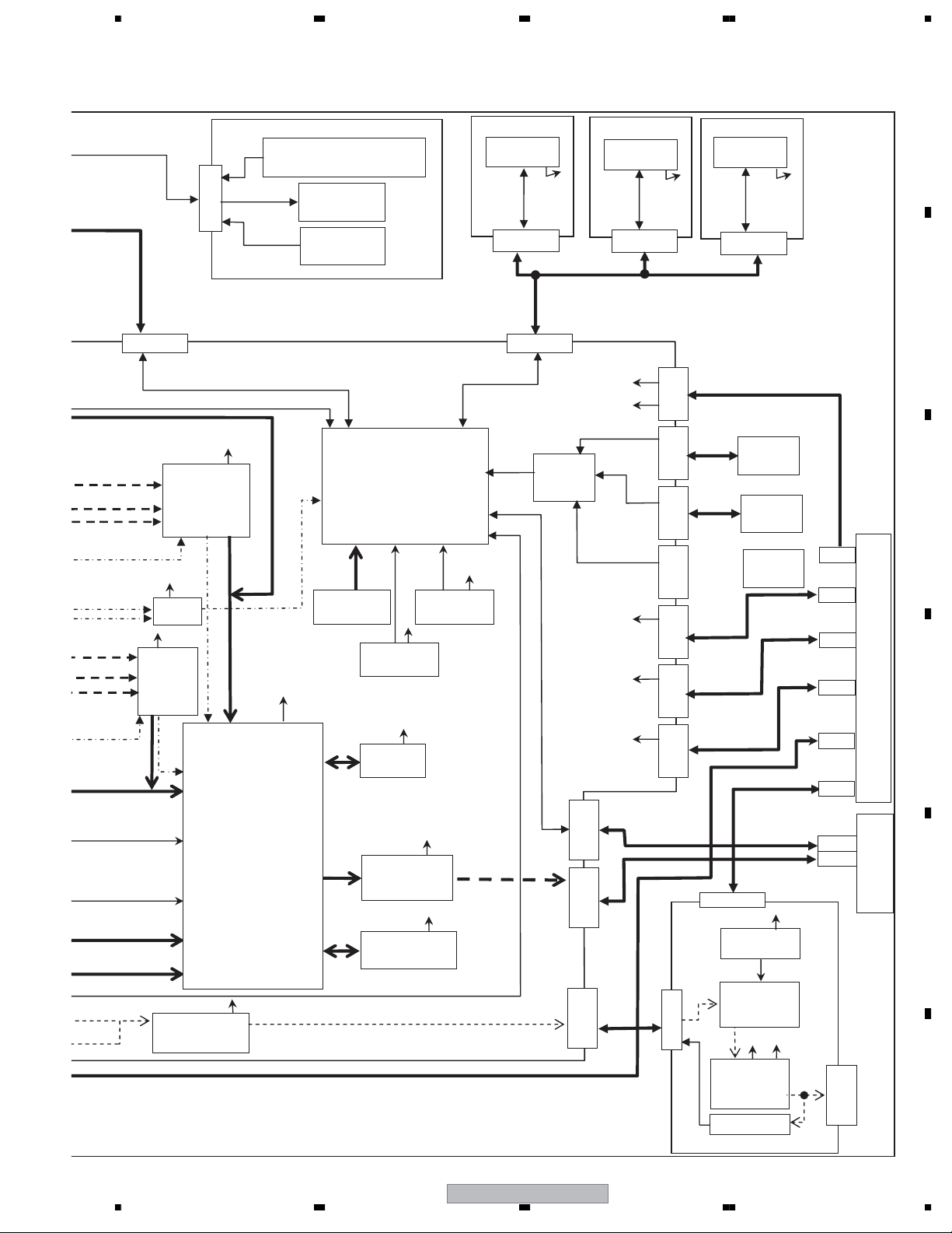
3.4 OVERALL BLOCK DIAGRAM (2/2)
General Block Diagram (2/2)
A
PDP Module
Scan Signal
VH
B
C
To MAIN (1/2)
IC2801
IC5V
Scan IC
PSUS
IC2802
Scan IC
IC2803
Scan IC
IC2804
Scan IC
IC2805
Scan IC
IC2806
Scan IC
CN2802
Serial Data
CN2702
IC2701
Scan IC
IC2702
Scan IC
IC2703
Scan IC
IC2704
Scan IC
IC2705
Scan IC
D1
G
H
D2
IC2706
Scan IC
PSUS
IC5V
VH
Scan Signal
SCAN B ASSY (UPPER)
VH
SB1
Y2
PSUS
PSUS
Y3
SA1
IC5V
VH
IC5V
Photo Coupler
VH VSUS
VH DC/DC Conv.
Vprst
Vprst Reg.
+5V +16.5V
VSUS
IC2252
Mask
Mod.
+5V
SUSOUT
VSUS
+5V
+16.5V
IC2253
Mask
Mod.
+16.5V
Soft-D
Block
IC5V
IC5V
Block
IC5V/VF
DC/DC
VF
Conv.
Vprst
+ Reset
Block
VOFS
Regulator
+16.5V
Resonance
Block
+5V
+16.5V
IC2101
DK Mod.
+16.5V
Scan Signal
VSUS
+6.5V
+5V
VOFS
DC/DC
Conv.
Y4
+5V
Logic
Block
Offset
Block
VOFS
+16.5V
Drive Signal
Y1
+5V
Y5
60V
Y6
P6 P1
V+8V
Block
V+ADR5
CLK/LE/HBLK/LBLK
IC1555
Driver IC
CN1501
AN/P BN/P
CN/P DN/P CLKN/P
R/G/B
Driver IC
IC1554
(PEE002A-K)
V+3V
LVDS Receiver
IC1501
AD1 AD2
D
Resonance
IC1553
Driver IC
CN1502
V+60VV+5V
Resonance
V+ADR1
IC1552
Driver IC
Block
AD1 AD2
Resonance
V+8V
Block
V+ADR5
CLK/LE/HBLK/LBLK
IC1555
Driver IC
CN1501
AN/P BN/P
CN/P DN/P CLKN/P
R/G/B
Driver IC
IC1554
(PEE002A-K)
V+3V
IC1501
LVDS Receiver
IC1553
Driver IC
CN1502
V+60VV+5V
Resonance
V+ADR1
IC1552
Driver IC
Block
P6 P1
Power Supply Unit AXY1127-
PV
E
A
To MAIN (1/2)
B
C
D
PM
PN
PA
+12V
+6V
+7V
+3.3V
+2.7V
+12V
E
F
PS
F
+3.3V
+12V
+3.3STB
P3
+16.5V
+6.5V
Vsus
+16.5V
+6.5V
Vsus
+8V
+STB3.3V
STB_MUTE_B
EXT_PD
VSUS_ADJ
PS_PD
RELAY
DRF_B
AC_DET
PD_TRIG_B
+60V
+60V
P1
P2
P4
P6
P7
+16.5V
30
PDP-425CMX
1234
Page 31

5678
A
V,sus_ADJ
V+3V_D
SCAN_PD
YDRV_PD
YSUS_PD
D10
YDD_PD
SCN5V_PD
Vots, ADJ, VYPAST_ADJ
SCAN
YSUS
D5
V+8V
V+8V
D6
D2 D1
SCL
SCA
DAC
Pulse
Width
OR
ADR_PD1
LVDS
Bus Buffer
V+3V STB
REM
STB_MT
CONNECTOR CONNECTOR
V+1V_D
PS_PWDN
SQ_PD
Mask
UART
SW
SCL, SDA
DC_DC Converier
(AXY1116)
OR
IC3154
(M30620FCPGP)
Module Ucom
(PEG122C-K)
Sequence Processor
FIELD
RA, GA, BA
LVDS RECEIVER
LVDS
V+3V ACT V+8V
Module
PD_
MUTE
IC3401
IC3001
P4
V+6V
PD
VD
HD
DCLK, DE
DCC
XSUS
PSIZE
H DET
D11
REPLAY,
PD_TRIGGER
AC_DET.
DRF
XSUSTN_PD
XDD_CW_PD
XDRIVE_PD
V+8V
V+8V
LVDS
IC3301
Flash Memory
Bus Buffer
P2 P7
SUS CLAMP 1
X DRIVE ASSY
D9
X1
D8
D7
X2
X4
Logic
Block
+16.5V
+6.5V
+16.5V +5V
IC1101
OK Mod.
Resonance
Block
Drive Signal
Regulator
VSUS
VSUS+5V
+5V
+16.5V
X3
SUS CLAMP 2
ASSY
+16.5V
SUS OUT
ASSY
VRN
DC/DC
Conv.
15V
DC/DC
Conv.
VSUS
-Reset
Block
+5V
IC1202
Mask
Mod.
VSUS
CL1
VRN
VSUS+16.5V
PSUS
VF
B
C
CL2
V+8V
Block
V+ADR5
CLK/LE/HBLK/LBLK
IC1555
Driver IC
CN1501
AN/P BN/P
CN/P DN/P CLKN/P
R/G/B
Driver IC
IC1554
(PEE002A-K)
V+3V
LVDS Receiver
IC1501
Driver IC
AD1 AD2
Resonance
IC1553
CN1502
P4
V+60VV+5V
Resonance
V+ADR1
IC1552
Driver IC
Block
V+8V
Block
V+ADR5
CLK/LE/HBLK/LBLK
IC1555
Driver IC
CN1501
AN/P BN/P
CN/P DN/P CLKN/P
R/G/B
Driver IC
IC1554
(PEE002A-K)
V+3V
LVDS Receiver
IC1501
Driver IC
AD1 AD2
Resonance
P2 P7
POWER SW
IC1553
CN1502
V+60VV+5V
Resonance
V+ADR1
Driver IC
Block
D
IC1552
E
F
56
PDP-425CMX
AC INLET
31
7
8
Page 32

1234
3.5 MAIN ASSY BLOCK DIAGRAM
Main Assy Block Diagram
A
MAIN ASSY
CN7001
INPUT2
B
C
CN5002
INPUT1
CN5003
ANALOG
RGB OUT
SlotAnalog Video Signal
#1
7V to 5V
#1,13
#15,19,21
#10,13,15
#3,5
#1,13
+7V
IC7006
IC5001
BUF
IC5002
IC5004
Video SW
IC5007
BUF
+5V
IC5008
BUF
+3.3V
IC7001
DVI
Receiver
5V to 3.3V
+3.3V
#4,10
+5V
+9V
IC5005
Sync SW
#4,10
#3
IC7003
#1,3,5
#7,9,11
+3.3V
#3,6
#2,5
#7,9,11
#1,3,5
#4,12
#6,10
#5,11
#7,9,11
#1,3,5
#6,10
#5,11
#4,12
IC5601
Video
SW
IC5603
Sync SW
IC5901
Video
SW
IC5902
Sync SW
+5V
+3.3V
+5V
+3.3V
#15,19,21
#7,9
#15,19,21
#7,9
LPF
#1,5,25
LPF
#2,5
#2,5
#3
#1,5,25
#3
IC5905
LPF
IC5903
Sync sep
IC5605
Sync sep
+5V
#11,14,17
+5V
IC5602
+5V
#11,13
LPF
#11,13
#5,2
#2,5
+5V
#3,6
#3,6
#2,5
IC5606
BUF
#11,14,17
IC5604
SW
+5V
#3,6
IC5904
SW
+3.3V
Slot Digital Video
D
CN5001
AV
Signal
CN6301
D1 D2
E
F
IC6301
OE
Slot Digital Video
Signal
CN6302
Control signal
Analog Video signal
Sync signal
Power Supply
CN5301
D3
Slot Audio Signal
IN PUT1
IN PUT2
OUT PUT
JA5371
JA5372
JA5373
Digital Video signal, CLK, Sync
TMDS, LVDS
Digital Audio signal
Analog Audio signal
#5, 8
#1, 6
#3, 7
+12V
IC5308
Audio
SW
#11, 15
32
PDP-425CMX
1234
Page 33

5678
#4,7
#9,12
#2,5
#22,30,37
#24,32,39
#18,20
SW
CN9011 CN9010
KEY #2
#22,30,37
#24,32,39
#18,20
#3,4,6,7,143,144
+6V
+3.3V
IC9504
BUF
IC6701
A/D
Converter
IC6501
A/D
Converter
#4
IC6502
6V to 3.3V
+3.3V
SDA,SCL
#118,119
+6V
+3.3V
SDA,SCL
#118,119
#17,4,
,98,3
#11,13
X9501
33.333MHz
IC9501
u-COM
#5
IC9502
7V to 5V
#4
IC9503
7V to 3.3V
+7V
TM
CN9501
Temp Sensor
SCL,SDA #1,4
#2
+7V
IC9001
FA N
Control
+12V
D9003,4
Alarm
detect
+12V
+6V
+7V
+3.3V
+2.5V
#1
#3,4
#1
#3
#1
#3
#1
#3
#1
#1,2,3
#1,2,3
CN9008
PV
FA
CN9004 CN9005 CN9003
FB
FC
CN9006
PM
CN9007
PN1
CN9012
PN2
A
B
C
#3,4,6,7,143,144
+3.3V
#4,7
IC8002
2.5V to 1.5V
IC8003
3.3V to 1.5V
X8001
X8002
+2.5V
+3.3V
IC6702
6V to 3.3V
#4
#5
#3,5
#4
Digital signal
IC5306
IC8001
Processor
+3.3V
+12V
DSP
Control
IC8105
OSD
#12,55,57,58
IC8101~8104
+3.3V
SDRAM
IC8501
LVDS
Transmitter
+3.3V
+3.3V
CN8502
AD2
D
CN8501
AD1
E
CN9001
AU
Audio Buffer
56
PDP-425CMX
F
33
7
8
Page 34

1234
3.6 COMMON SLOT ASSY
A
+5V
#120
#118,#119
#114,#115
#106
#20
#105
#19
#16
+3.3V
+6.5V
RXD PDP
TXD CARD
TXD PDP
RXD CARD
B
IC2007
#10
#8 #9
#2
#1
IC2006
#3
#2
IC2007
#5
#4
#6
#11
IC2007
#12
#13
IC2007
#3
#1
C
#6
#4
CN2004
#4
#108
IR COMM IN
CB MUTE
FIRST RXD
#3
#2
IRSW
IR COMM OUT
#4
#5
IC2005
#6
#9
#10
IC2005
#8
#18
INT EXT
IC2005
#12
#13
IC2005
#11
#17
GET UART
#1
#3
#125
G4/G5
#2
#122
APL RXD
#8
IC2001
#9
#10
#121
APL CTL1
IC2001
#123
APL CTL2
#2
IC2002
#3
#2
#3
#124
APL TXD
#13
#12
IC2002
#11
#109
STL LINK
IC2006
#5
#6
#11
IC2001
#12
#13
#1
#2
D
#3
#11
#8
#10
#4
#5
IC2004
#6
#13
#10
#12
IC2004
#9
#15
E
#19
+3.3V
232C
IC2003
MAX3222
IC2001
#5
#4
#12
#8
IC2002
#9
#13
#10
#6
IC2002
#4
#5
Driver/Receiver
#8
#2
#17
#9
#3
#16
#5
#3
#2
#4
#6
#5
#3
#4
#2
#6
used only by the slot of external vender.
F
SUB ASSY (1/3)
COMM SLOT ASSY
34
1234
CN2001
External
Controle
PDP-425CMX
JA2002
JA2003
Combination In
Combination Out
Page 35

5678
3.7 KEY, LED, SENB, SENC and SEND ASSYS
SUB ASSY (2/3)
KEY ASSY
+3.3V
S2201
to S2208
Matrix
SW
LED ASSY
+5V
U2401
Remote Control
Receiver
D2402
LED
+3V
#1
D2401
Photo IC Diode
#20
#7
#8
#9
#10
#11
#12
#13
#3
#1
REMIN
IC2201
Key Micro Com
+3.3V
+5V
#19
#6
#8
#1
CN2401
LEDCTL1, LEDCTL2
#2,#3
RLS
#2,#3
#5
KEY
+3.3V
#1
#2
CN2201
A
B
C
SENC ASSY
+3.3V
#8
IC1101
TEMP
Sensor
SENB ASSY
+3.3V
#8
IC1001
TEMP
Sensor
SEND ASSY
+3.3V
#8
IC1201
TEMP
Sensor
#1,#2
#1,#2
#1,#2
SCL,SDA
SCL,SDA
SCL,SDA
+3.3V
#3,#4
+3.3V
#5
#5
CN1101
CN1001
D
E
#3,#4
+3.3V
#5
CN1201
#3,#4
F
56
PDP-425CMX
35
7
8
Page 36

1234
3.8 AUDIO and SUS COMM IF ASSYS
SUB ASSY (3/3)
A
AUDIO ASSY
+12V
IC3001
12V to 9V
+9V
CN3004
L/R
#2, 27 #11, 19
IC3001
Audio
L/R
Controller
B
Audio Controle
ALM #5
COMM I/F ASSY
SCL,SDA
#17, 18
Mute
#9
+5V
IC2301
#1
CN2301
#2
C
#3
#5
#9
REMIN
LED CTL1
LED CTL2
RLS
#11
#1
#10
#13,#2
CN3003
+12V
IC3002
Audio
Amplifier
#14
IRSW
IR COMM OUT
IR COMM IN
+9V
+12V
#6
#31, 32
#36, 38
#41, 43
#47, 48
R+
R-
L+
L-
DC detect
#2
#3
#4
#7
#6
#16,#13
#2
D
E
#15,#20
#21,#25
CN2302
#29
#17
#34,#36,#38,#39,#40
#4,#14
F
REMIN
+3.3V
+6.5V
+5V
#1
#33,#35
#19,#23
#27
#31
#30,#32
#24
#26,#28
VCC DOWN2
RXD,TXD(RXD PDP,TXD PDP)
PLE CTL PLE CTL2(APL CTL,APL CTL2)
RXD2,TXD2(APL RXD,APL TXD)
STL LINK
CB MUTE
4G/5GSLT VER
KEY(KEY COMM IN)
RXD GU,TXD GU (RXD CARD,TXD CARD)
FIRST RXD
INT EXT,GET UART
GPC1~GPC5
CSL ST1,CSL ST2
*
*
*
* used only by the slot of external vender.
Detection of
6.5V decrease
#105,#106
#121,#123
#122#124
*
*
#21,#22,#23,#24,#25
#19,#20
#17,#18
#10,#11
CN2303
#109
#108
#125
#107
#16
36
PDP-425CMX
1234
Page 37

5678
A
B
C
D
E
56
PDP-425CMX
F
37
7
8
Page 38

1234
3.9 POWER BLOCK DIAGRAM
A
B
C
INPUT1 SCHMITT
IC5002(LVC14A)
A_SYNC_SEL&5to3
IC5604(LCX157)
F5025
9→6.5 COMM SLOT
IC9002(PQ200WNA1ZPH)
digi (TDA8754)
F6504
digi (TDA8754)
F6704
D
EDID ROM
IC5003(BR24C21F)
A_SYNC_SEP
IC5605(BA7078)
DSUB_OUT_BUF
IC5606(LVC2G126)
DSUB_OUT_BUF
IC5008(LVC2G126)
DVI RECEIVER
IC7001(SII1169)
A_SYNC_SEL
B_RGB_SEL
IC5901(BA7657)
A_LPF
IC5602(SM5301)
B_LPF
IC5905(SM5301)
DSUB_OUT_SEL
IC5004(BA7657)
IN1_DETTrB_SYNC_SEP
IC5903(BA7078)
B_SYNC_SEL&5to3
IC5904(LCX157)
B_SYNC_SEL
IC5902(VHC153)
IC5603(VHC153)
E
IC9001(PQ20WZIU)
POMUTE
PULL UP
AUDIO AMP
IC5306(NJM4580)
AUDIO SW
IC5308(NJM2750)
12→9 VCC+9V FB VCC+9V_2 DSUB OUT
IC5303(NJM78M09DL1A) IC5007(EL5362)
IC5009(BA05FP) IC5601(BA7657)
6→3.3 VCC+3.3ADA FB ana A_AD
IC6502(NJM2846DL3-33) digi IC6501
6→3.3 VCC+3.3ADB FB ana B_AD
IC6702(NJM2846DL3-33) digi IC6701
IC5006(NJM2846DL3-05) IC5301(BU2152)
7→55→3 VDD+3S R VDD+3SA A_SYNC_SW
IC7006(PQ20WZ1U) IC7003(PQ20WZ1U) IC9504(LVC08)
FU9002
A+12 IP VCC+12V 12→VARIABLE FAN
PV FU9001
F
POWER
SUPPLY
ASSY
38
A+6V IP VCCA+6V 6→5 VCC+5V A_RGB_SEL
M+7 IP VDDM7 7V→5V VCC+5S I/O EXP
PM FU9003
PDP-425CMX
1234
Page 39

5678
A
PROCESSOR
D+3.3 R VDD3.3 IP VDD3.3P FB OSD IC
PN FU8003 F8103
IC8105(MB90098)
F8003
FB VDD3.3PS DIGITAL SIGNAL
L8001 PL_AVDD1
L8004 PL_AVDD2
VDD1.5DLL
FU8002 F8002 IC8001(PASTEL)
3.3V→1.5V IP FB
IC8003(PQ1MX55M2SPQ)
L8002 RIP_DVDD
L8003 RSC_DVDD
IC8101(K4S643232H)
F8101
FB 64M SDRAM
IC8102(K4S643232H)
F8104
FB 64M SDRAM
F8102
IC8103(K4S643232H)
FB 64M SDRAM
F8105
FB 64M SDRAM
IC8104(K4S643232H)
X8002(143M)
F8004
FB X
F8005
X8001(90M)
FB X
IC8501(THC63LVD103)
F8501
FB VDD_3.3V_LV LVDS Transmitter
FU6301 F6301
IC6301(PD6435)
IP FB VDD3.3E IC6 OE_IC
FU8001 F8001
IC8001(PASTEL)
IC8002(SI-3011ZD) PROCESSOR
D+2.5 R VDD2.5 IP FB 2.5V→1.5V VDD1.5P DIGITAL SIGNAL
P1
+16.5V
A+12.0V IP VIDEO SLOT
PS FU4001
IC4003(PQ200WNA1ZPH)
A+13.5V 16.5V→13.5V
D+3.3V
B
C
STB3.3V
IC9507(RTC-4543)
BT9501 RTC
7V→5V VDDM5 LED ASSY
COMM SLOT I/F
IC9502(PQ1U501M2ZP)
7V→3.3V VDDM3.3V MAIN CPU
I/O EXP2
IC5304(MAX7313)
IC9503(NJM2846DL3-33) IC9501(M30700)
RESET
IC9505(BD4727)
SLOT IN SCHMITT
IC5001(LV14A)
EEPROM
IC9508(24LC128SN)
RTC
IC9507(RTC-4543)
COMM SLOT
LED ASSY
KEY CONT
IC2201(PD5719)
232C SEL
IC8503(LCX157)
D
E
F
12.7V
56
PDP-425CMX
39
7
8
Page 40

1234
3.10 CONNECTOR PIN DESCRIPTION
A
(Caution)The operating voltages specified below are used in common inspective of the presence of signals. In this case, however, part of the oprating voltages(red characters)may change according to the
signal conditions when the main power supply is turned on(POWER botton ON).
Status of LED lighting: for lighting in Green, for unlighting, and for lighting in red.
Name Function
PN1
CN9007
PN2
CN9012
B
PN
PM
C
CN9006
PM
PV
CN9008
D
PV
AU
CN9001
CN3004
E
TM
CN9501
F
12
11
10
1
2
3
4
5
6
1
2
3
4
5
6
7
9
8
7
6
5
4
3
2
1
1
2
3
4
5
6
7
7
6
5
4
3
2
1
1
2
3
4
5
6
7
8
8
7
6
5
4
3
2
1
1
2
3
4
5
6
7
8
9
1
2
3
Pin namePin No.
D+3.3
3.3V power supply for
digital circuits
D+3.3
3.3V power supply for
digital circuits
D+3.3
3.3V power supply for
digital circuits
D.GND
GND
D.GND
GND
D.GND
GND
D+2.5
2.5V power supply for
digital circuits
D+2.5
2.5V power supply for
digital circuits
D+2.5
2.5V power supply for
digital circuits
NC
Non-connection termial
D.GND
GND
D.GND
GND
D.GND
GND
D+3.3
3.3V power supply for
digital circuits
D+3.3
3.3V power supply for
digital circuits
D+3.3
3.3V power supply for
digital circuits
D.GND
GND
D.GND
GND
D.GND
GND
D+2.7
2.7V power supply for
digital circuits
D+2.7
2.7V power supply for
digital circuits
D+2.7
2.7V power supply for
digital circuits
D.GND
GND
D.GND
GND
D.GND
GND
M+7
7V power supply for
microcomputer
D.GND
GND
NC
Non-connection termial
NC
Non-connection termial
NC
Non-connection termial
NC
Non-connection termial
NC
Non-connection termial
M+7
7V power supply for
microcomputer
D.GND
GND
NC
Non-connection termial
NC
Non-connection termial
NC
Non-connection termial
NC
Non-connection termial
NC
Non-connection termial
A+12
12V power supply for
analog circuits
A.GND
GND
A+6
6V power supply for
analog circuits
A+6
6V power supply for
analog circuits
A.GND
GND
A.GND
GND
NC
Non-connection termial
NC
Non-connection termial
A+12
12V power supply for
analog circuits
A.GND
GND
A+6
6V power supply for
analog circuits
A+6
6V power supply for
analog circuits
A.GND
GND
A.GND
GND
NC
Non-connection termial
NC
Non-connection termial
AU_L
Audio signal L CH
GND
GND
AU_R
Audio signal R CH
GND
GND
SP_ALM
Audio output alarm signal
GND
GND
MUTE
Mute signal of audio output
SCL7
Clock line of the I2C bus
SDA7
Data line of the I2C bus
SCL5
Clock line of the I2C bus
GND
GND
VDD+3.3V
3.3V power supply for analog signals
MAIN
MAIN
MAIN
MAIN
MAIN
MAIN
MAIN
MAIN
MAIN
MAIN
MAIN
MAIN
MAIN
PSU
PSU
PSU
PSU
PSU
PSU
PSU
PSU
PSU
PSU
PSU
PSU
MAIN
MAIN
MAIN
MAIN
MAIN
MAIN
MAIN
PSU
PSU
PSU
PSU
PSU
PSU
PSU
MAIN
MAIN
MAIN
MAIN
MAIN
MAIN
MAIN
MAIN
PSU
PSU
PSU
PSU
PSU
PSU
PSU
PSU
Basic operation(Numerical unit:Vdc; except for case when units are individually indicated)
AC power ON
(Power cord
connected to the
wall outlet)
MAIN POWER "ON"
No signal
0
0
0
0
0
0
0
0
0
0
0
0
0
0
0
0
0
0
0
0
0
0
0
0
0
0
-
-
-
-
0
0
-
-
-
-
0
0
0
0
0
0
-
0
0
0
0
0
0
-
0
0
0
0
0
0
0
04.59.0
4.5V (4 sec.)
at power on.
0
Clock signal
(5Vac) when
data are
received; 5Vdc
when no data
are received.
0
Clock signal
(5Vac) when
data are
received; 5Vdc
when no data
are received.
0
clock signal
use during data
transmission
(3.3Vac),3.3Vdc
when no data
are transmitted
0
0
With signal
3.3
3.3
3.3
0
0
0
2.5
2.5
2.5
0
0
0
3.3
3.3
3.3
0
0
0
2.7
2.7
2.7
0
0
0
6.8
0
-
-
-
-
7
0
-
-
-
-
-
12
0
6
6
0
0
-
-
12
0
6
6
0
0
-
0
input signals
0
0
0
3.3
0
04.59.0
4.5V (4 sec.)
at power on.
(5Vac) when
received; 5Vdc
when no data
are received.
(5Vac) when
received; 5Vdc
when no data
are received.
use during data
transmission
(3.3Vac),3.3Vdc
when no data
are transmitted
0
3.3
Selected
are output
Selected
input signals
are output
Clock signal
data are
Clock signal
data are
clock signal
3.3
3.3
3.3
0
0
0
2.5
2.5
2.5
0
0
0
3.3
3.3
3.3
0
0
0
2.7
2.7
2.7
0
0
0
6.8
0
-
-
-
-
7
0
-
-
-
-
-
12
0
6
6
0
0
-
-
12
0
6
6
0
0
-
-
0
0
3.3
0
0
3.3
Power
management
Standby Main power
0
0
0
0
0
0
0
0
0
0
0
0
0
0
0
0
0
0
0
0
0
0
0
0
6.8
0
-
-
-
-
7
0
-
-
-
-
0
0
0
0
0
0
-
0
0
0
0
0
0
-
0
0
0
0
3.3
0
0
0
1
0
0
0
0
0
0
0
0
0
0
0
0
0
0
0
0
0
0
0
0
0
0
0
0
0
0
0
6.8
0
-
-
-
-
7
0
-
-
-
-
0
0
0
0
0
0
-
0
0
0
0
0
0
-
0
0
0
0
3.3
0
0
0
1
0
0
0
OFF
AC Power OFF
(Power cord pulled
out of the wall outlet
0
0
0
0
0
0
0
0
0
0
0
0
0
0
0
0
0
0
0
0
0
0
0
0
0
0
-
-
-
-
0
0
-
-
-
-
0
0
0
0
0
0
-
0
0
0
0
0
0
-
0
0
0
0
0
0
0
0
0
0
0
0
0
0
0
0
0
0
0
0
0
0
0
0
0
0
0
0
0
0
0
0
0
0
0
0
0
0
-
-
-
-
0
0
-
-
-
-
0
0
0
0
0
0
-
0
0
0
0
0
0
-
0
0
0
0
0
0
0
0
0
0
0
0
Signal direction
(DR : Data Relay)
POWERMAIN
POWERMAIN
POWERMAIN
-
-
-
POWERMAIN
POWERMAIN
POWERMAIN
-
-
-
-
POWERMAIN
POWERMAIN
POWERMAIN
-
-
-
POWERMAIN
POWERMAIN
POWERMAIN
-
-
-
POWERMAIN
-
-
-
-
-
-
POWERMAIN
-
-
-
-
-
-
POWERMAIN
-
POWERMAIN
POWERMAIN
-
-
-
-
POWERMAIN
-
POWERMAIN
POWERMAIN
-
-
-
-
MAINAUDIO
-
MAINAUDIO
-
AUDIOMAIN
-
MAINAUDIO
MAINAUDIO
MAINAUDIO
MAINSENB
-
MAINSENB
40
PDP-425CMX
1234
Page 41

5678
Name
TM2
CN1001
TM3
CN1201
TM4
CN1101
FA
CN9003
FB
CN9004
4
1
2
3
4
5
6
7
8
1
2
3
4
5
6
7
8
1
2
3
4
1
2
3
1
2
Pin namePin No.
SDA5
SCL5
GND
VDD+3.3V
SDA5
SCL5
GND
VDD+3.3V
SDA5
SCL5
GND
VDD+3.3V
SDA5
SCL5
GND
VDD+3.3V
SDA5
SCL5
GND
VDD+3.3V
SDA5
FAN-CTL
GND
F_ALM
FAN-CTL
GND
Function
Data line of the I2C bus
Clock line of the I2C bus
GND
3.3V power supply for analog signals
Data line of the I2C bus
Clock line of the I2C bus
GND
3.3V power supply for analog signals
Data line of the I2C bus
Clock line of the I2C bus
GND
3.3V power supply for analog signals
Data line of the I2C bus
Clock line of the I2C bus
GND
3.3V power supply for analog signals
Data line of the I2C bus
Clock line of the I2C bus
GND
3.3V power supply for analog signals
Data line of the I2C bus
Voltage- controllable power supply
GND
Fan lock detect signal output
Voltage- controllable power supply
GND
Basic operation(Numerical unit:Vdc; except for case when units are individually indicated)
"AC power ON
(Power cord
connected to the
wall outlet) "
MAIN POWER "ON"
No signal
0
During data
exchange: Clock
signal (3.3Vac),
datanot
exchanged:
3.3Vdc
0
Clock signal
used during
transmission
(3.3Vac), 3.3Vdc
when no data
are transmitted
0
0
0
During data
exchange:
Clock signal
(3.3Vac),datanot
exchanged:
3.3Vdc
0
Clock signal
during data
transmission
(3.3Vac), 3.3Vdc
when no data
are transmitted
0
0
0
During data
exchange:
Clock signal
(3.3Vac),datanot
exchanged:
3.3Vdc
0
Clock signal
during data
transmission
(3.3Vac), 3.3Vdc
when no data
are transmitted
0
0
0
During data
exchange:
Clock signal
(3.3Vac),datanot
exchanged:
3.3Vdc
0
Clock signal
during data
transmission
(3.3Vac), 3.3Vdc
when no data
are transmitted
0
0
0
During data
exchange:
Clock signal
(3.3Vac),datanot
exchanged:
3.3Vdc
0
Clock signal
used during
transmission
(3.3Vac),
3.3Vdc when
no data
are transmitted
0
0
0
During data
exchange:
Clock signal
(3.3Vac),datanot
exchanged:
3.3Vdc
0
11.6Vdc during
high-speed
revolition
(Fan mode H) ;
8.8Vdc during
medium speed
revolition
(Fan mode M) ;
6.0Vdc during
low-speed
revolition
(Fan mode L) ;
0
0
0V during
normal Fan
operation;
3.3Vdc while
the fan is
stopped
0
11.6Vdc during
high-speed
revolition
(Fan mode H) ;
8.8Vdc during
medium
speed revolition
(Fan mode M) ;
6.0Vdc during
low-speed
revolition
(Fan mode L)
0
data
used
used
used
data
0
3.3
0
3.3
0
3.3
0
3.3
0
3.3
0
0
With signal
During data
exchange: Clock
signal (3.3Vac),
datanot
exchanged:
3.3Vdc
Clock signal
used during
data
transmission
(3.3Vac), 3.3Vdc
when no data
are transmitted
During data
exchange:
Clock signal
(3.3Vac),datanot
exchanged:
3.3Vdc
Clock signal
used during
data
transmission
(3.3Vac), 3.3Vdc
when no data
are transmitted
During data
exchange:
Clock signal
(3.3Vac),datanot
exchanged:
3.3Vdc
Clock signal
used during
data
transmission
(3.3Vac), 3.3Vdc
when no data
are transmitted
During data
exchange:
Clock signal
(3.3Vac),datanot
exchanged:
3.3Vdc
Clock signal
used
during data
transmission
(3.3Vac), 3.3Vdc
when no data
are transmitted
During data
exchange:
Clock signal
(3.3Vac),datanot
exchanged:
3.3Vdc
Clock signal
used during
data
transmission
(3.3Vac),
3.3Vdc when
no data are
transmitted
During data
exchange:
Clock signal
(3.3Vac),datano
t exchanged:
3.3Vdc
11.6Vdc during
high-speed
revolition
(Fan mode H)
;8.8Vdc during
medium speed
revolition
(Fan mode M) ;
6.0Vdc during
low-speed
revolition
(Fan mode L) ;
0V during
normal Fan
operation;
3.3Vdc while
the fan is
stopped
11.6Vdc during
high-speed
revolition
(Fan mode H) ;
8.8Vdc during
medium speed
revolition
(Fan mode M) ;
6.0Vdc during
low-speed
revolition
(Fan mode L)
0
3.3
0
3.3
0
3.3
0
3.3
0
3.3
0
0
"Power
management
"
Standby "Main power
0
0
0
0
0
0
0
0
0
0
0
0
0
0
0
0
0
0
0
0
0
0
0
0
0
0
0
0
0
0
0
0
0
0
0
0
0
0
0
0
0
0
0
0
0
0
0
0
0
0
0
0
OFF
"
"AC Power OFF
(Power cord pulled
out of the wall outlet
"
0
0
0
0
0
0
0
0
0
0
0
0
0
0
0
0
0
0
0
0
0
0
0
0
0
0
0
0
0
0
0
0
0
0
0
0
0
0
0
0
0
0
0
0
0
0
0
0
0
0
0
0
"Signal direction
(DR : Data Relay)"
MAINSENB
MAINSENB
-
MAINSENB
MAINSENB
SENBSEND
-
SENBSEND
SENBSEND
SENBSEND
-
SENBSEND
SENBSEND
SENDSENC
-
SENDSENC
SENDSENC
SENDSENC
-
SENDSENC
SENDSENC
MAINFAN
-
FANMAIN
MAINFAN
-
A
B
C
D
E
F
56
PDP-425CMX
41
7
8
Page 42

1234
A
Name
AD1
CN8501
B
Pin namePin No.
3
F_ALM
1
GND
2
GND
3
GND
4
RE+
5
RE-
6
RD+
7
RD-
8
RCLK+
9
RCLK-
Fan lock detect signal output
GND
GND
GND
Video system output E+
Video system output E-
Video system output D+
Video system output D-
Video system output clock+
Video system output clock-
Function
C
10
GND
11
RC+
12
RC-
13
RB+
14
15
16
17
18
19
20
21
22
23
24
25
26
27
28
29
30
31
32
33
1
2
3
4
6
7
8
9
RB-
RA+
RA-
GND
NC
NC
NC
NC
NC
NC
GND
MSEL
POWER
STB_MUTE
RFU
STATUS
GND
GND
GND
GND
GND
GND
P_ST_B
MR_ST_B
MR_RXD
NC
AC_DET_B
NC
D
E
AD2
CN8502
F
GND
Video system output C+
Video system output C-
Video system output B+
Video system output B-
Video system output A+
Video system output A-
GND
Non-connection termial
Non-connection termial
Non-connection termial
Non-connection termial
Non-connection termial
Non-connection termial
GND
Module function grade select signal
POWER ON SIGNAL
Stand by power control signal
GND
Non-connection termial
GND
GND
GND
GND
GND
GND
Connecting detection (PDPMAIN)
Connecting detection (MAINPDP)
UART data (PDPMAIN)
Non-connection termial
AC power detection from power supply
Non-connection termial
Basic operation(Numerical unit:Vdc; except for case when units are individually indicated)
"AC power ON
(Power cord
connected to the
wall outlet) "
MAIN POWER "ON"
No signal
0
0V during
normal Fan
operation;
3.3Vdc
while the fan is
stopped
0
0
0
0
Video mode
LVDS serial
differential E+
output 0Vac;
Bias 1.1Vdc
0
Video mode
LVDS serial
differential E output 0Vac;
Bias 1.4Vdc
0
Video mode
LVDS serial
differential D+
output 0Vac;
Bias 1.1Vdc
0
Video mode
LVDS serial
differential D-
output 0Vac;
Bias 1.4Vdc
0
Video data
clock
LVDS serial
differential
clock+
output 0.3Vac;
Bias 1.25Vdc
0
Video data
clock LVDS
differential
clock-
output 0.3Vac;
Bias 1.25Vdc
0
0
data LVDS
differential C+
output 0.3Vac:
Bias 1.25Vdc
0
data LVDS
differential C-
output 0.3Vac:
Bias 1.25Vdc
0
data LVDS
differential B+
output 0Vac:
Bias 1.1Vdc
0
data LVDS
differential B-
output 0Vac:
Bias 1.4Vdc
0
data LVDS
differential A+
output 0Vac:
Bias 1.1Vdc
0
data LVDS
differential A-
output 0Vac:
Bias 1.4Vdc
0
-
-
-
-
-
0
0
0
0
0
0
0
0
0
0
0
0
0
0
Clock signal
(3.3Vac) when
are received;
3.3Vdc
when no data
are received.
0
-
serial
Video
serial
Video
serial
Video
serial
Video
serial
Video
serial
Video
serial
3.3V
data
With signal
norma Fan
operation;
while the fan is
0
0
0
Video mode
LVDS serial
differential E+
output 0.3Vac;
Bias 1..25Vdc
Video mode
LVDS serial
differential E-
output 0.3Vac;
Bias 1..25Vdc
Video mode
LVDS serial
differential D+
output 0.3Vac;
Bias 1.25Vdc
Video mode
LVDS serial
differential D-
output 0.3Vac;
Bias 1.25Vdc
Video data
LVDS serial
differential
output 0.3Vac;
Bias 1.25Vdc
Video data
clock LVDS
differential
output 0.3Vac;
Bias 1.25Vdc
0
data LVDS
differential C+
output 0.3Vac:
Bias 1.25Vdc
data LVDS
differential C-
output 0.3Vac:
Bias 1.25Vdc
data LVDS
differential B+
output 0.3Vac:
Bias 1..25Vdc
data LVDS
differential B-
output 0.3Vac:
Bias 1.25Vdc
data LVDS
differential A+
output 0.3Vac:
Bias 1..25Vdc
data LVDS
differential A-
output 0.3Vac:
Bias 1.25Vdc
0
-
-
-
-
-
0
0
0
0
0
0
0
0
0
0
0
0
Clock signal
(3.3Vac) when
are received;
when no data
are received.
0
-
0V during
3.3Vdc
stopped
clock
clock+
serial
clock-
Video
serial
Video
serial
Video
serial
Video
serial
Video
serial
Video
serial
3.3V
data
3.3Vdc
management
0
0
0
0
0
-
-
-
-
-
0
0
0
0
0
0
0
0
0
0
0
0
0
-
"Power
"
Standby "Main power
0
0
0
0
0
0
0
0
0
0
0
0
0
0
0
0
0
0
-
-
-
-
-
0
0
3.3V
0
0
0
0
0
0
0
0
0
0
0
0
-
3.3V
0
0
0
0
0
0
0
0
0
0
0
0
0
0
0
0
0
0
-
-
-
-
-
0
0
0
0
0
0
0
0
0
0
0
0
0
0
-
OFF
"
"AC Power OFF
(Power cord pulled
out of the wall outlet
"
0
0
0
0
0
0
0
0
0
0
0
0
0
0
0
0
0
0
-
-
-
-
-
0
0
0
0
0
0
0
0
0
0
0
0
0
0
0
-
0
0
0
0
0
0
0
0
0
0
0
0
0
0
0
0
0
0
-
-
-
-
-
0
0
0
0
0
0
0
0
0
0
0
0
0
0
0
-
"Signal direction
(DR : Data Relay)"
FANMAIN
-
-
-
MAINPDP
MAINPDP
MAINPDP
MAINPDP
MAINPDP
MAINPDP
-
MAINPDP
MAINPDP
MAINPDP
MAINPDP
MAINPDP
MAINPDP
-
-
-
-
-
-
-
-
-
MAINPDP
-
-
-
-
-
-
-
PDPMAIN
MAINPDP
PDPMAIN
PDPMAIN
-
42
PDP-425CMX
1234
Page 43

5678
Name
"SW
CN9011
CN2201"
PA
CN3003
PA
CN9010
CN2302
10
11
12
13
14
15
16
17
18
19
20
1
2
3
1
2
3
4
5
6
6
5
4
3
2
1
1
2
3
4
5
6
7
8
9
10
11
12
13
14
15
16
17
18
19
20
21
22
23
24
Pin namePin No.
REQ
NC
MR_TXD
NC
STB_MUTE
NC
VIS
NC
FIELD
GND
GND
VDDM3
KEY
GND
S+12
S+1
S+12
GND
GND
GND
S+12
S+12
S+12
GND
GND
GND
VCC_DOWN2
V+6.5V
NC
CSL_ST1
NC
REMIN
LEDCTL1
GND
LEDCTL2
CYOBL2
RLS
CYOBL1
VDDM3.3V
CSL_ST2
VDDM5
VDDM3.3V
4G/5G
GND
TXD2
VDDM5
PLE_CTL2
GND
RXD2
FIRST_RXD
Function
UART send request from PDP module
Non-connection termial
UART data (MAINPDP)
Non-connection termial
Stand by power control signal
Non-connection termial
reserve
Non-connection termial
Adbanced cinema controle signal
GND
GND
Key input detection
GND
12V power supply
audio circuits
12V power supply
audio circuits
12V power supply
audio circuits
GND
GND
GND
12V power supply
audio circuits
12V power supply
audio circuits
12V power supply
audio circuits
GND
GND
GND
6.5V voltage surveillance
6.5V power supply for analog circuits
Non-connection termial
SLOT DETECT
Non-connection termial
Infrared remote control data
LED(RED)
GND
LED(GREEN)
Non-connection termial
Optical sensor
Non-connection termial
3.3V power supply for microcomputer
SLOT TYPE DETECT
5V power supply for microcomputer
3.3V power supply for microcomputer
Generation information
GND
PLE LINK
5V power supply for microcompute
PLE LINK process select
GND
PLE LINK
RXD signal
(to V-CARD's micro_COM only)
MAIN
MAIN
MAIN
MAIN
MAIN
MAIN
PSU
PSU
PSU
PSU
PSU
PSU
Basic operation(Numerical unit:Vdc; except for case when units are individually indicated)
"AC power ON
(Power cord
connected to the
wall outlet) "
MAIN POWER "ON"
No signal
0
3.3Vdc when
riquest signal
is received;
0Vdc when no
riquest signal
is received.
-
0
Clock signal
(3.3Vac) when
are received;
0Vdc when
no data are
received.
-
0
-
0
0
0
0
0
0
0.7~2.8Vdc
When key
inputs are
enterd; 3.3Vdc
no key inputs
are enterd.
0
0
0
0
0
0
0
0
0
0
0
0
0
0
"6.5V normal
3.3Vdc,
6.5V unusual
0Vdc"
0
-
0
-
0
Clock signal
(5Vac)
when data are
received; 5Vdc
when no data
are received.
0
0
0
-
0
"Illumination
100lx 1Vdc
Illumination
200lx 2Vdc"
0
0
0
0
0
0
0
clock signal
used duaring
transmission
(5Vac), 5Vdc
when no data
transmitted.
0
0
High output
3.3Vdc, Low
output 0Vdc
0
0
Clock signal
(5Vac) when
data are
received; 5Vdc
when no data
are received.
0
clock signal
used duaring
data recieved
(3.3Vac),
3.3Vdc
when no data
are received.
data
when
12.5
12.5
12.5
12.5
12.5
12.5
6.5V
3.3V
3.3V
3.3V
3.3V
data
are
0
0
0
0
0
3.3
0
0
0
0
0
0
0
0
0
5V
5V
0
0
5V
0
With signal
3.3Vdc when
riquest signal
is received;
0Vdc when no
riquest signal is
received.
Clock signal
(3.3Vac) when
data are
received;
0Vdc when
no data are
received.
-
-
-
0.7~2.8Vdc
When key
inputs are
enterd; 3.3Vdc
no key inputs
are enterd.
"6.5V normal
3.3Vdc,
6.5V unusual
-
Clock signal
(5Vac) when
data are
received; 5Vdc
when no data
are received.
"Illumination
100lx 1Vdc
Illumination
200lx 2Vdc"
-
clock signal
used duaring
transmission
(5Vac), 5Vdc
when no data
transmitted.
High output
3.3Vdc, Low
output 0Vdc
Clock signal
(5Vac) when
data are
received; 5Vdc
when no data
are received.
clock signal
used duaring
data recieved
(3.3Vac),
when no data
are received.
when
12.5
12.5
12.5
12.5
12.5
12.5
0Vdc"
6.5V
3.3V
3.3V
3.3V
3.3V
data
are
3.3Vdc
management
-
-
0
-
0
0
0
0
3.3
enterd; 3.3Vdc
no key inputs
0
0
0
0
0
0
0
-
-
(5Vac) when
received; 5Vdc
when no data
are received.
0
0
5V
-
100lx 1Vdc
-
5V
0
0
used duaring
transmission
(5Vac), 5Vdc
when no data
5V
3.3Vdc, Low
output 0Vdc
0
(5Vac) when
received; 5Vdc
when no data
are received.
used duaring
data recieved
when no data
are received.
"Power
"
4.7
3.3
0.7~2.8Vdc
When key
inputs are
when
are enterd.
3.3V
Clock signal
data are
"Illumination
Illumination
200lx 2Vdc"
3.3V
3.3V
3.3V
clock signal
data
are
transmitted.
High output
Clock signal
data are
clock signal
(3.3Vac),
3.3Vdc
Standby "Main power
0
-
0
-
-
0
0
0
0
0.7~2.8Vdc
When key
inputs are
enterd; 3.3Vdc
when
no key inputs
are enterd.
0
0
0
0
0
0
0
0
0
0
0
0
0
0
0
-
3.3V
Clock signal
(5Vac) when
data are
received;5Vdc
when no data
are received.
5V
0
0
"Illumination
100lx 1Vdc,
Illumination
200lx 2Vdc"
-
3.3V
0
0
clock signal
used duaring
transmission
(5Vac), 5Vdc
when no data
transmitted.
0
Clock signal
(5Vac) when
received; 5Vdc
when no data
are received.
clock signal
used duaring
data recieved
(3.3Vac),
when no data
are received.
3.3V
3.3V
data
data are
3.3Vdc
5V
5V
0
-
0
-
4.7
-
0
0
0
0
3.3
0
0
0
0
0
0
0
0
0
0
0
0
0
0
0
-
-
5V
0
0
-
-
5V
0
0
are
5V
0
0
OFF
"
"AC Power OFF
(Power cord pulled
out of the wall outlet
"
0
-
0
-
0
-
0
0
0
0
0
0
0
0
0
0
0
0
0
0
0
0
0
0
0
0
0
0
0
0
0
0
0
0
0
0
0
0
0
0
0
0
0
0
0
"Signal direction
(DR : Data Relay)"
0
PDPMAIN
-
0
MAINPDP
-
0
MAINPDP
-
0
MAINPDP
-
0
MAINPDP
0
0
0
MAINKEY
0
KEYMAIN
0
0
POWERAUDIO
0
POWERAUDIO
0
POWERAUDIO
0
0
0
0
POWERAUDIO
0
POWERAUDIO
0
POWERAUDIO
0
0
0
0
COMM SLOT I/FMAIN
0
MAINCOMM SLOT I/F
-
0
COMM SLOT I/FMAIN
-
0
COMM SLOT I/FMAIN
0
MAINCOMM SLOT I/F
0
0
MAINCOMM SLOT I/F
-
0
COMM SLOT I/FMAIN
-
0
MAINCOMM SLOT I/F
0
COMM SLOT I/FMAIN
0
MAINCOMM SLOT I/F
0
MAINCOMM SLOT I/F
0
COMM SLOT I/FMAIN
0
0
MAINCOMM SLOT I/F
0
MAINCOMM SLOT I/F
0
MAINCOMM SLOT I/F
0
0
COMM SLOT I/FMAIN
0
COMM SLOT I/FMAIN
A
-
-
-
-
-
-
-
-
-
-
B
C
-
-
-
-
-
-
-
-
-
D
E
-
56
PDP-425CMX
F
43
7
8
Page 44

1234
A
Name
25
26
27
28
Pin namePin No.
PLE_CTL
GET_UART
STL_LINK
INT_EXT
Function
PLE LINK process select
U-ART process select
The signal for still picture detection
linkage operation
U-ARTÅ in/out Select
B
29
30
31
32
CB_MUTE
RXD_GU
KEY
TXD_GU
COMBINATION MUTEÅ signal
RXD signal(by GET_UART)
KEY SCAN Signal
TXD Signal(by GET_UART)
C
33
RXD
34
GPC5
35
TXD
36
D
CN2303
CN2004
37
38
39
40
1
2
3
4
GPC4
GND
GPC3
GPC1
GPC2
NC
IRSW
IR_COMM_
OUT
IR_COMM_IN
RXD Siganal(to PDPÅfs micro_COM)
COMM CARD-VIDEO CARD I/F
TXD signal
(from PDP's micro_COM)
COMM CARD-VIDEO CARDÅ
Exclusive communication line
GND
COMM CARD-VIDEO CARDÅ
Exclusive communication line
COMM CARD-VIDEO CARDÅ
Exclusive communication line
COMM CARD-VIDEO CARDÅ
Exclusive communication line
Non-connection termial
IR signa process select
Infrared remote control data output
(to PDP's micro_COM)
Infrared remote control data input
(from IR)
E
5
6
7
8
9
10
11
14
15
16
17
GND
GND
GND
CYOBI3
CYOBI2
CSL_ST2
CSL_ST1
GND
GND
FIRST_RXD
GET_UART
GND
GND
GND
Non-connection termial
Non-connection termial
SLOT TYPE DETECT
SLOT DETECT
GND
GND
"RXDsignal
(to V-CARD's micro_COM only)
U-ART PROCESSÅ SELECT
F
Basic operation(Numerical unit:Vdc; except for case when units are individually indicated)
"AC power ON
(Power cord
connected to the
wall outlet) "
MAIN POWER "ON"
No signal
0
High output
3.3Vdc, Low
output 0Vdc
0
3.3Vdc::232C
connector
PDP, 0V:
232Cconnecto
VIDEO:
CARD,
PDPVIDEO
CARD
0
STL_LINK OFF
signal(3.3Vdc),
STL_LINK ON
signal(0Vdc)
0
0V:232C
connector
VIDEO CARD,
3.3Vdc:
PDPVIDEO
CARD
0
MUTE OFF
signal(3.3Vdc),
MUTE ON
signal(0Vdc)
0
clock signal
used duaring
data recieved
(3.3Vac),
3.3Vdc when
no data are
received.
0
clock signal
used duaring
data recieved
(3.3Vac),
3.3Vdc when
no data are
received.
0
Clock signal
used during
transmission
(3.3Vac),
3.3Vdc when
no data are
transmitted
0
clock signal
used duaring
data recieved
(3.3Vac),
3.3Vdc when
no data are
received.
0
0
Clock signal
during data
transmission
(3.3Vac),
3.3Vdc when
no data are
transmitted
0
0
0
0
0
0
0
Clock signal
(4Vac) when
are received;
5Vdc when
no data are
received.
0
clock signal
used duaring
transmission
(4Vac), 5Vdc
when no data
are transmitted.
0
0
0
-
0
0
0
0
0
clock signal
used duaring
data recieved
(3.3Vac),
3.3Vdc when
no data are
received.
0
V:232C
connector
VIDEO CARD,
3.3Vdc:
PDPVIDEO
data
used
data
data
3.3V
3.3V
CARD
0
0
0
0
0
0
5V
0
0
0
0
0
With signal
High output
3.3Vdc, Low
output 0Vdc
3.3Vdc::232C
connector
PDP, 0V:
232Cconnecto
VIDEO
CARD,
PDPVIDEO
CARD
STL_LINK OFF
signal(3.3Vdc),
STL_LINK ON
signal(0Vdc)
0V:232C
connector
VIDEO CARD,
3.3Vdc:
PDPVIDEO
CARD
MUTE OFF
signal(3.3Vdc),
MUTE ON
signal(0Vdc)
clock signal
used duaring
data recieved
(3.3Vac),
3.3Vdc when
no data are
received.
clock signal
used duaring
data recieved
(3.3Vac),
3.3Vdc when
no data are
received.
Clock signal
used during
transmission
(3.3Vac),
3.3Vdc when
no data are
transmitted
clock signal
used duaring
data recieved
(3.3Vac),
3.3Vdc when
no data are
received.
Clock signal
during data
transmission
(3.3Vac),
3.3Vdc when
no data are
transmitted
-
Clock signal
(4Vac) when
are received;
5Vdc when
no data are
received.
clock signal
used duaring
transmission
(4Vac), 5Vdc
when no data
are transmitted.
-
-
clock signal
used duaring
data recieved
(3.3Vac),
3.3Vdc when
no data are
received.
V:232C
connector
VIDEO CARD,
3.3Vdc:
PDPVIDEO
CARD
STL_LINK OFF
signal(3.3Vdc),
PDPVIDEO
data
0
used
0
0
0
0
0
-
5V
data
data
are transmitted.
0
0
0
-
-
3.3V
3.3V
0
0
PDPVIDEO
"Power
management
"
High output
3.3Vdc, Low
output 0Vdc
3.3Vdc::232C
connector
PDP, 0V:
232Cconnecto
VIDEO
CARD,
PDPVIDEO
CARD
STL_LINK ON
signal(0Vdc)
0V:232C
connector
VIDEO CARD,
3.3Vdc:
CARD
MUTE OFF
signal(3.3Vdc),
MUTE ON
signal(0Vdc)
clock signal
used duaring
data recieved
(3.3Vac),
3.3Vdc when
no data are
received.
clock signal
used duaring
data recieved
(3.3Vac),
3.3Vdc when
no data are
received.
Clock signal
used during
data
transmission
(3.3Vac),
3.3Vdc when
no data are
transmitted
clock signal
used duaring
data recieved
(3.3Vac),
3.3Vdc when
no data are
received.
Clock signal
used
during data
transmission
(3.3Vac),
3.3Vdc when
no data are
transmitted
Clock signal
(4Vac) when
data
are received;
5Vdc when
no data are
received.
clock signal
used duaring
data
transmission
(4Vac), 5Vdc
when no data
3.3V
3.3V
clock signal
used duaring
data recieved
(3.3Vac),
3.3Vdc when
no data
are received.
V:232C
connector
VIDEO CARD,
3.3Vdc:
CARD
Standby "Main power
3.3Vdc::232C
connector
PDP, 0V:
232Cconnecto
VIDEO
CARD,
PDPVIDEO
CARD
STL_LINK OFF
signal(3.3Vdc),
STL_LINK ON
signal(0Vdc)
0V:232C
connector
VIDEO CARD,
3.3Vdc:
PDPVIDEO
CARD
MUTE OFF
signal(3.3Vdc),
MUTE ON
signal(0Vdc)
clock signal
used duaring
data recieved
(3.3Vac),
3.3Vdc when
no data are
received.
clock signal
used duaring
data recieved
(3.3Vac),
3.3Vdc when
no data are
received.
Clock signal
used during
data
transmission
(3.3Vac),
3.3Vdc when
no data are
transmitted
clock signal
used duaring
data recieved
(3.3Vac),
3.3Vdc when
no data are
received.
0
Clock signal
used
during data
transmission
(3.3Vac),
3.3Vdc when
no data are
transmitted
0
0
0
0
0
-
5V
0
0
0
-
-
0
0
Clock signal
(4Vac) when
data
are received;
5Vdc when
no data are
received.
clock signal
used duaring
data
transmission
(4Vac), 5Vdc
when no data
are transmitted.
3.3V
3.3V
clock signal
used duaring
data recieved
(3.3Vac),
3.3Vdc when
no data are
received.
0V:232C
connector
VIDEO CARD,
3.3Vdc:
PDPVIDEO
CARD
5V
0
0
0
0
0
0
0
-
0
0
0
-
-
0
0
OFF
"
"AC Power OFF
(Power cord pulled
out of the wall outlet
0
0
0
0
0
0
0
0
0
0
0
0
0
0
0
0
0
0
0
0
0
0
-
0
0
0
0
0
0
"
0
MAIN COMM SLOT I/F
0
MAINCOMM SLOT I/F
0
MAINCOMM SLOT I/F
0
MAINCOMM SLOT I/F
0
MAINCOMM SLOT I/F
0
COMM SLOT I/FMAIN
0
MAINCOMM SLOT I/F
0
MAINCOMM SLOT I/F
0
COMM SLOT I/FMAIN
0
MAINOMM SLOT I/F
0
MAINCOMM SLOT I/F
0
MAINOMM SLOT I/F
0
0
MAINOMM SLOT I/F
0
MAINOMM SLOT I/F
0
MAINOMM SLOT I/F
0
COMM CARDCOMM SLOT I/F
0
COMM CARDCOMM SLOT I/F
0
COMM SLOT I/FCOMM CARD
0
0
0
-
0
COMM CARDCOMM SLOT I/F
0
COMM CARDCOMM SLOT I/F
0
0
0
COMM CARDCOMM SLOT I/F
0
COMM SLOT I/FCOMM CARD
"Signal direction
(DR : Data Relay)"
-
-
-
-
-
-
-
-
-
44
PDP-425CMX
1234
Page 45

5678
Name
CN2301
CN2401
101
102
103
104
105
106
107
108
109
110
111
114
115
116
117
118
119
120
121
122
123
124
125
18
19
20
21
22
23
24
25
1
2
3
4
5
Pin namePin No.
INT_EXT
RXD_CARD
TXD_CARD
GPC5
GPC4
GPC3
GPC2
GPC1
NC
GND
GND
GND
TXD_PDP
RXD_PDP
KEY_
COMM_IN
CB_MUTE
STL_LINK
GND
GND
V+6.5V
V+6.5V
GND
GND
VDDM3.3V
VDDM3.3V
VDDM5V
APL_CTL1
APL_RXD
APL_CTL2
APL_TXD
SLT_Ver
REMIN
LEDCTL1
LEDCTL2
GND
RLS
Function
U-ART in/out Select
RXD signal(by GET_UART)
TXD signal(by GET_UART)
COMM CARD-VIDEO CARD
Exclusive communication line
COMM CARD-VIDEO CARD
Exclusive communication line
COMM CARD-VIDEO CARD
Exclusive communication line
COMM CARD-VIDEO CARD
Exclusive communication line
COMM CARD-VIDEO CARD
Exclusive communication line
Non-connection termial
GND
GND
GND
TXD signal
(from PDPÅfs micro_COM)
RXD signal (to PDPÅfs micro_COM)
KEY SCAN signal
COMBINATION MUTE signal
The signal for still picture detection
linkage operation
GND
GND
6.5V power supply for analog circuits
6.5V power supply for analog circuits
GND
GND
3.3V power supply for microcomputer
3.3V power supply for microcomputer
5V power supply for microcomputer
PLE LINK process select
PLE LINK
PLE LINK process select
PLE LINK
Generation information
Infrared remote control data
LED(RED)
LED(GREEN)
GND
Optical sensor
Basic operation(Numerical unit:Vdc; except for case when units are individually indicated)
"AC power ON
(Power cord
connected to the
wall outlet) "
MAIN POWER "ON"
No signal
0
connector
VIDEO CARD,
PDPVIDEO
0
clock signal
used duaring
data recieved
3.3Vdc when
no data are
0
Clock signal
during data
transmission
3.3Vdc when
no data are
transmitted
0
0
0
0
-
0
0
0
0
0
Clock signal
used during
transmission
3.3Vdc when
no data are
transmitted
0
clock signal
used duaring
data recieved
3.3Vdc when
are received.
0
Clock signal
used during
transmission
3.3Vdc when
are transmitted
0
MUTE OFF
signal(3.3Vdc),
signal(0Vdc)
0
STL_LINK OFF
signal(3.3Vdc),
STL_LINK ON
signal(0Vdc)
0
0
0
0
0
0
0
0
0
0
High output
3.3Vdc Low,
output 0Vdc
0
Clock signal
(5Vac) when
received; 5Vdc
when no data
are received.
0
High output
3.3Vdc Low
output 0Vdc
0
clock signal
duaring data
transmission
5Vdc when
no data are
transmitted.
0
0
Clock signal
(4.4Vac) when
are received;
4.4Vdc when
are received.
0
0
0
0
Illumination
100lx 1Vdc,
Illumination
200lx 2Vdc"
0V::232C
3.3Vdc:
CARD
(3.3Vac),
received.
used
(3.3Vac),
data
(3.3Vac),
(3.3Vac),
no data
data
(3.3Vac),
no data
MUTE ON
6.5V
6.5V
3.3V
3.3V
data are
used
(5Vac),
data
no data
With signal
connector
VIDEO CARD,
PDPVIDEO
clock signal
used duaring
data recieved
3.3Vdc when
no data are
Clock signal
during data
transmission
3.3Vdc when
no data are
transmitted
0
0
0
0
0
0
0
0
Clock signal
used during
transmission
3.3Vdc when
no data are
transmitted
clock signal
used duaring
data recieved
3.3Vdc when
are received.
Clock signal
during data
transmission
3.3Vdc when
are transmitted
MUTE OFF
signal(3.3Vdc),
MUTE ON
signal(0Vdc)
"STL_LINK OFF
signal(3.3Vdc),
STL_LINK ON
signal(0Vdc)
0
0
0
0
5V
High output
3.3Vdc Low,
output 0Vdc
Clock signal
(5Vac) when
received; 5Vdc
when no data
are received.
High output
3.3Vdc Low
output 0Vdc
clock signal
duaring data
transmission
5Vdc when
no data are
transmitted.
0
Clock signal
(4.4Vac) when
are received;
4.4Vdc when
are received.
0
5V
0
Illumination
100lx 1Vdc,
Illumination
200lx 2Vdc"
0V::232C
3.3Vdc:
CARD
(3.3Vac),
received.
used
(3.3Vac),
data
(3.3Vac),
(3.3Vac),
no data
used
(3.3Vac),
no data
6.5V
6.5V
3.3V
3.3V
data are
used
(5Vac),
data
no data
"Power
management
"
connector
VIDEO CARD,
PDPVIDEO
clock signa
l used duaring
data recieved
3.3Vdc when
no data are
Clock signal
during data
transmission
3.3Vdc when
no data are
transmitted
0
0
0
0
0
0
0
0
Clock signal
used during
transmission
3.3Vdc when
no data are
transmitted
clock signa
l used duaring
data recieved
(3.3Vac),
3.3Vdc when
are received.
Clock signal
during data
transmission
3.3Vdc when
are transmitted
MUTE OFF
signal(3.3Vdc),
MUTE ON
signal(0Vdc)
"STL_LINK OFF
signal(3.3Vdc),
STL_LINK ON
signal(0Vdc)
0
0
0
0
5V
High output
3.3Vdc Low,
output 0Vdc
Clock signal
(5Vac) when
received; 5Vdc
when no data
are received.
High output
3.3Vdc Low
output 0Vdc
clock signal
duaring data
transmission
5Vdc when
no data are
transmitted.
0
Clock signal
(4.4Vac) when
are received;
4.4Vdc when
are received.
0
5V
0
Illumination
100lx 1Vdc,
Illumination
200lx 2Vdc"
0V::232C
3.3Vdc:
CARD
(3.3Vac),
received.
used
(3.3Vac),
data
(3.3Vac),
no data
used
(3.3Vac),
no data
3.3V
3.3V
data are
used
(5Vac),
data
no data
Standby "Main power
0V::232C
connector
VIDEO CARD,
3.3Vdc:
PDPVIDEO
CARD
clock signal
used duaring
data recieved
(3.3Vac),
3.3Vdc when
no data are
received.
Clock signal
used
during data
transmission
(3.3Vac),
3.3Vdc when
no data are
transmitted
0
0
0
0
0
0
0
0
Clock signal
used during
data
transmission
(3.3Vac),
3.3Vdc when
no data are
transmitted
clock signal
used duaring
data recieved
(3.3Vac),
3.3Vdc when
no data
are received.
Clock signal
used during
data
transmission
(3.3Vac),
3.3Vdc when
no data
are transmitted
MUTE OFF
signal(3.3Vdc),
MUTE ON
signal(0Vdc)
STL_LINK OFF
signal(3.3Vdc),
STL_LINK ON
signal(0Vdc)
0
0
0
0
0
0
3.3V
Clock signal
(5Vac) when
data are
received; 5Vdc
when no data
are received.
clock signal
duaring data
transmission
5Vdc when
no data are
transmitted.
0
Clock signal
(4.4Vac) when
are received;
4.4Vdc when
are received.
0
0
Illumination
100lx 1Vdc,
Illumination
200lx 2Vdc"
3.3V
used
(5Vac),
data
no data
5V
5V
5V
5V
0
0
0
0
0
0
0
0
0
0
0
0
0
0
0
0
0
0
0
OFF
"
"AC Power OFF
(Power cord pulled
out of the wall outlet
"
0
0
0
0
0
0
0
0
0
0
0
0
0
0
0
0
0
0
0
0
0
0
0
0
0
0
0
0
0
0
0
0
0
0
0
"Signal direction
(DR : Data Relay)"
0
COMM SLOT I/FCOMM CARD
0
COMM CARDCOMM SLOT I/F
0
COMM SLOT I/FCOMM CARD
0
COMM SLOT I/FCOMM CARD
0
COMM SLOT I/FCOMM CARD
0
COMM SLOT I/FCOMM CARD
0
COMM SLOT I/FCOMM CARD
0
COMM SLOT I/FCOMM CARD
0
0
0
0
COMM SLOT I/FCOMM CARD
0
COMM CARDCOMM SLOT I/F
0
COMM SLOT I/FCOMM CARD
0
COMM SLOT I/FCOMM CARD
0
COMM SLOT I/FCOMM CARD
0
0
0
COMM SLOT I/FCOMM CARD
0
COMM SLOT I/FCOMM CARD
0
0
0
COMM SLOT I/FCOMM CARD
0
COMM SLOT I/FCOMM CARD
0
COMM SLOT I/FCOMM CARD
0
COMM SLOT I/FCOMM CARD
0
COMM CARDCOMM SLOT I/F
0
COMM SLOT I/FCOMM CARD
0
COMM SLOT I/FCOMM CARD
0
COMM CARD COMM SLOT I/F
0
0
0
0
0
-
-
-
-
-
-
-
-
LED2COMM SLOT I/F
COMM SLOT I/FLED2
COMM SLOT I/FLED2
-
LED2COMM SLOT I/F
A
B
C
D
E
F
56
PDP-425CMX
45
7
8
Page 46

1234
A
Name
AV
CN5001
B
C
AV
CN4005
D
D3
CN5301
6
7
8
1
2
3
4
5
6
7
8
9
10
11
12
13
14
15
16
17
18
19
20
19
20
17
18
15
16
13
14
11
12
9
10
7
8
5
6
3
4
1
2
1
2
3
4
5
6
Pin namePin No.
VDDM3.3V
GND
VDDM5V
SLOT_VD
GND
GND
AUDIO_L
SLOT_HD
GND
GND
AUDIO_R
R(R-Y)
GND
GND
NC
B(B-Y)
GND
GND
NC
Y(G)ON_
SYNC
GND
GND
NC
VD_SA
GND
GND
AUDIO_L
HD_SA
GND
GND
AUDIO_R
R(R-Y)
GND
GND
NC
B(B-Y)
GND
GND
NC
Y(G)ON_
SYNC
GND
GND
NC
NC
PNP_WR
VCC_
DOWN1
GND
SCL5
SDA5
Function
3.3V power supply for microcomputer
GND
5V power supply for microcomputer
VD for ANALOG
SYNC
GND
GND
AUDIO L ch
HD for ANALOG
SYNC
GND
GND
AUDIO R ch
RED(Cr or Pr) for
ANALOG
GND
GND
Non-connection termial
BLUE(Cb or Pb) for
ANALOG
GND
GND
Non-connection termial
GREEN(Y) for
ANALOG(on Sync)
GND
GND
Non-connection termial
VD for ANALOG
SYNC
GND
GND
AUDIO L ch
HD for ANALOG
SYNC
GND
GND
AUDIO R ch
RED(Cr or Pr) for
ANALOG
GND
GND
Non-connection termial
BLUE(Cb or Pb) for
ANALOG
GND
GND
Non-connection termial
GREEN(Y) for
ANALOG(on Sync)
GND
GND
Non-connection termial
Non-connection termial
EEPROM WRITE
PROTECT
VIDEO CARD voltage
surveillance
GND
Clock line of the
I2C bus
Data line of the
I2C bus
MAIN
MAIN
MAIN
MAIN
MAIN
MAIN
MAIN
MAIN
MAIN
MAIN
MAIN
MAIN
MAIN
MAIN
MAIN
MAIN
MAIN
MAIN
MAIN
MAIN
VIDEO SLOT I/F
VIDEO SLOT I/F
VIDEO SLOT I/F
VIDEO SLOT I/F
VIDEO SLOT I/F
VIDEO SLOT I/F
VIDEO SLOT I/F
VIDEO SLOT I/F
VIDEO SLOT I/F
VIDEO SLOT I/F
VIDEO SLOT I/F
VIDEO SLOT I/F
VIDEO SLOT I/F
VIDEO SLOT I/F
VIDEO SLOT I/F
VIDEO SLOT I/F
VIDEO SLOT I/F
VIDEO SLOT I/F
VIDEO SLOT I/F
VIDEO SLOT I/F
MAIN
MAIN
MAIN
MAIN
MAIN
MAIN
E
7
SCL_VS
8
SDA_VS
9
GND
10
IN4_DET
F
Clock line of the
I2C bus
Data line of the
I2C bus
GND
INPUT4 SIGNAL
DETECT for AUTO
POWER OFF
MAIN
MAIN
MAIN
MAIN
Basic operation(Numerical unit:Vdc; except for case when units are individually indicated)
AC power ON
(Power cord
connected to the
wall outlet)
MAIN POWER "ON"
No signal
0
0
0
Synchronized
signal of
SLOT HIGH
MIN 2.4V,
LOW MAX 0.9V
0
0
0
0
0
0
0
0
0
0
-
0
0
0
-
0
0
0
-
0
0
0
0
0
0
0
0
0
0
0
-
0
0
0
-
0
0
0
-
-
0
0
Normal 3.3Vdc,
unusual 0Vdc
0
0
Clock signal
used during
transmission
(3.3Vac),
3.3Vdc when
no data are
transmitted
0
During data
exchange:
Clock signal
(3.3Vac),
datanot
exchanged:
3.3Vdc
0
Clock signal
used during
transmission
(3.3Vac),
3.3Vdc when
no data are
transmitted
0
During data
exchange:
Clock signal
(3.3Vac),
datanot
exchanged:
3.3Vdc
0
0
When INPUT4
signal
is inputted. 0V,
When INPUT4
signal is
not inputted,
5Vdc
3.3V
0
5V
LOW MAX 0.9V
0
0
0
0
LOW MAX 0.9V
0
0
0
0
0
0
-
0
0
0
-
0
0
0
-
0
LOW MAX 0.9V
0
0
0
0
LOW MAX 0.9V
0
0
0
0
0
0
-
0
0
0
-
0
0
0
-
-
0
Normal 3.3Vdc,
0
data
data
0
is inputted. 0V,
With signal
3.3V
Synchronized
signal of
SLOT HIGH
MIN 2.4V,
Audio signal
of SLOT
Synchronized
signal of
SLOT HIGH
MIN 2.4V,
Audio signal
of SLOT
Video signal
0.7Vp-p
Video signal
0.7Vp-p
Video signal
0.7~1.0Vp-p
Synchronized
signal of
SLOT HIGH
MIN 2.4V,
Audio signal
of SLOT
Synchronized
signal of
SLOT HIGH
MIN 2.4V,
Audio signal
of SLOT
Video signal
0.7Vp-p
Video signal
0.7Vp-p
Video signal
0.7~1.0Vp-p
unusual 0Vdc
Clock signal
used during
data
transmission
(3.3Vac),
3.3Vdc when
no data are
transmitted
During data
exchange:
Clock signal
(3.3Vac),
datanot
exchanged:
3.3Vdc
Clock signal
used during
data
transmission
(3.3Vac),
3.3Vdc when
no data are
transmitted
During data
exchange:
Clock signal
(3.3Vac),
datanot
exchanged:
3.3Vdc
When INPUT4
signal
When INPUT4
signal is
not inputted,
5Vdc
0
5V
0
0
0
0
0
0
-
0
0
-
0
0
-
0
0
0
0
0
0
-
0
0
-
0
0
-
-
0
0
0
Power
management
3.3V
Standby Main power
3.3V
0
5V
0
0
0
0
0
0
0
0
0
0
0
-
0
0
0
-
0
0
0
-
0
0
0
0
0
0
0
0
0
0
0
-
0
0
0
-
0
0
0
-
-
0
0
0
0
0
0
0
0
0
0
5V
0
0
0
0
0
0
0
0
0
0
0
-
0
0
0
-
0
0
0
-
0
0
0
0
0
0
0
0
0
0
0
-
0
0
0
-
0
0
0
-
-
0
0
0
0
0
0
0
0
0
OFF
AC Power OFF
(Power cord pulled
out of the wall outlet
0
0
0
0
0
0
0
0
0
0
0
0
0
0
-
0
0
0
0
0
0
0
0
0
0
0
0
0
0
0
0
0
0
0
0
0
0
0
-
0
0
0
0
0
0
0
0
0
Signal direction
(DR : Data Relay)
0
COMM SLOT I/FLED2
0
0
COMM SLOT I/FLED2
0
VIDEO SLOT I/FMAIN
0
0
0
VIDEO SLOT I/FMAIN
0
VIDEO SLOT I/FMAIN
0
0
0
VIDEO SLOT I/FMAIN
0
VIDEO SLOT I/FMAIN
0
0
VIDEO SLOT I/FMAIN
0
0
0
-
0
VIDEO SLOT I/FMAIN
0
0
-
0
VIDEO SLOT I/FMAIN
0
0
0
VIDEO SLOT I/FMAIN
0
VIDEO SLOT I/FMAIN
0
0
0
VIDEO SLOT I/FMAIN
0
VIDEO SLOT I/FMAIN
0
0
-
0
VIDEO SLOT I/FMAIN
0
0
-
0
VIDEO SLOT I/FMAIN
0
0
-
-
0
MAINVIDEO SLOT I/F
0
VIDEO SLOT I/FMAIN
0
0
MAINVIDEO SLOT I/F
0
MAINVIDEO SLOT I/F
0
MAINVIDEO SLOT I/F
0
MAINVIDEO SLOT I/F
0
0
VIDEO SLOT I/FMAIN
-
-
-
-
-
-
-
-
-
-
-
-
-
-
-
-
-
-
-
-
-
-
-
-
-
-
-
-
-
-
46
PDP-425CMX
1234
Page 47

5678
Name
11
12
13
14
15
16
17
18
19
20
21
22
23
24
25
26
27
28
29
30
31
32
33
34
3
36
37
38
39
40
41
42
43
44
Pin namePin No.
SLOT_ST1
S_DIN_SEL
FNC1
SLOT_ST2
IR
FNC0
G4G
DSUBSW_
DET
GND
VYOBI2
VYOBI1
GND
GPC5
GPC2
GPC4
GPC1
GPC3
HYOUJI_X
GND
IN5_HD
IN5_VD
GND
SOUND1
FNC2
FNC3
SOUND2
SD_SEL
SLOT_ST3
RESETX1
GND
INT_EXT
RXD_CARD
FIRST_RXD
TXD_CARD
Function
CARD TYPE SELECT
Digital INPUT
SELECTOR
FUNCTION LOGIC
CARD DETECT for
OEM/PIONEER
Infrared remote
control data
FUNCTION LOGIC
3G4G
DISCERMMENT
INPUT1VIDEO
CARD ANALOG
OUT SELECT
GND
NC
RESERVE
GND
VIDEO CARD
COMM CARD LINE
VIDEO CARD
COMM CARD LINE
VIDEO CARD
COMM CARD LINE
VIDEO CARD
COMM CARD LINE
VIDEO CARD
COMM CARD LINE
2 SCREENS
Permit/Prohibit
GND
INPUT5 SYNC
INPUT5 SYNC
GND
VIDEO CARD
AUDIO SELECT
VIDEO select
VIDEO select
VIDEO CARD
AUDIO SELECT
DIGITAL SIGNAL
FORMAT SELECT
CARD TYPE SELECT
RESET
GND
IF U / 232C SELECT
UART chosen
by GET_UART
RXD Direct to 232C
UART chosen
by GET_UART
MAIN
MAIN
MAIN
MAIN
MAIN
MAIN
MAIN
MAIN
MAIN
MAIN
MAIN
MAIN
MAIN
MAIN
MAIN
MAIN
MAIN
MAIN
MAIN
MAIN
MAIN
MAIN
MAIN
MAIN
MAIN
MAIN
MAIN
MAIN
MAIN
MAIN
MAIN
MAIN
MAIN
MAIN
AC power ON
(Power cord
connected to the
wall outlet)
INPUT5 SYNC
INPUT5 SYNC
MAIN POWER "ON"
No signal
0
When equipped
with PDA-
5003. 0V,When
equipped
with PDA-
5004 0.36Vdc
0
SLOT digital
ON 0V,SLOT
digita OFF
3.3Vdc
0
INPUT3,5
select 5Vdc,
INPUT4
select 0V
0
PIONEER
CARD:.3Vdc
OEM CARD:
0
Clock signal
(4.4Vac) when
are received;
4.4Vdc when
no data
are received.
0
INPUT4.5
select 5Vdc,
INPUT3
select 0V
0
When equipped
with 3G
CARD. 0V,
When equipped
with 4G
CARD. 3.3Vdc
0
3.3Vdc:
INPUT1
select,0V:
VIDEO CARD
0
0
0
0
0
0
0
0
0
Permit 0Vdc,
Prohibit
3.3Vdc
0
0
0
INPUT4,5
Audio select
3.4Vdc
0
INPUT3
select 0Vdc,
INPUT4,5
select 3.3Vdc
0
INPUT4
select 0Vdc,
INPUT3,5
select 3.3Vdc
0
INPUT3,5
Audio select
3.4Vdc
0
A/D Input
Port, No
VIDEO CARD
3.3Vdc
0
A/D Input
Port, No
VIDEO CARD
0
RESET
0V,Release
RESET 3.3Vdc
0
0
0V: 232C
CONNECTO
RVIDEO
CARD,3.3Vdc:
PDP
VIDEO CARD
0
clock signa
l used duaring
data recieved
(3.3Vac),
3.3Vdc when
no data
are received.
0
clock signa
l used duaring
data recieved
(3.3Vac),
3.3Vdc when
no data
are received.
0
Clock signal
during data
transmission
(3.3Vac),
3.3Vdc when
no data
are transmitted
0V
data
select
3.3V
3.3Vd
used
With signal
When equipped
with PDA-
5003. 0V,When
equipped
with PDA-
5004 0.36Vdc
SLOT digital
ON 0V,SLOT
digita OFF
INPUT3,5
select 5Vdc,
INPUT4
select 0V
PIONEER
CARD:.3Vdc
OEM CARD:
Clock signal
(4.4Vac) when
are received;
4.4Vdc when
are received.
INPUT4.5
select 5Vdc,
INPUT3
select 0V
When equipped
CARD. 0V,
When equipped
CARD. 3.3Vdc
select,0V:
VIDEO CARD
0
-
0
0
0
0
0
0
Permit 0Vdc,
0
0
INPUT5 SYNC
0
INPUT5 SYNC
0
INPUT4,5
Audio select
select 0Vdc,
INPUT4,5
select 3.3Vdc
select 0Vdc,
INPUT3,5
select 3.3Vdc
INPUT3,5
Audio select
A/D Input
Port, No
VIDEO CARD
A/D Input
VIDEO CARD
0V,Release
RESET 3.3Vdc
0
0V: 232C
CONNECTO
RVIDEO
CARD,3.3Vdc:
VIDEO CARD
clock signa
l used duaring
data recieved
(3.3Vac),
3.3Vdc when
are received.
clock signa
l used duaring
data recieved
(3.3Vac),
3.3Vdc when
are received.
Clock signal
during data
transmission
(3.3Vac),
3.3Vdc when
are transmitted
3.3Vdc
0V
data
no data
with 3G
with 4G
3.3Vdc:
INPUT1
select
3.3V
Prohibit
3.3Vdc
3.4Vdc
INPUT3
INPUT4
3.4Vdc
3.3Vdc
Port, No
3.3Vd
RESET
PDP
no data
no data
used
no data
management
When equipped
5003. 0V,When
5004 0.36Vdc
SLOT digital
ON 0V,SLOT
select 5Vdc,
CARD:.3Vdc
OEM CARD:
(4.4Vac) when
are received;
4.4Vdc when
are received.
select 5Vdc,
When equipped
When equipped
CARD. 3.3Vdc
VIDEO CARD
0
-
0
0
0
0
0
0
Permit 0Vdc,
0
INPUT5 SYNC
INPUT5 SYNC
0
Audio select
select 0Vdc,
select 3.3Vdc
select 0Vdc,
select 3.3Vdc
Audio select
VIDEO CARD
VIDEO CARD
0V,Release
RESET 3.3Vdc
0
CONNECTO
CARD,3.3Vdc:
VIDEO CARD
l used duaring
data recieved
3.3Vdc when
are received.
l used duaring
data recieved
3.3Vdc when
are received.
transmission
3.3Vdc when
are transmitted
Basic operation(Numerical unit:Vdc; except for case when units are individually indicated)
PDP-425CMX
56
Power
with PDA-
equipped
with PDA-
digita OFF
3.3Vdc
INPUT3,5
INPUT4
select 0V
PIONEER
Clock signal
data
no data
INPUT4.5
INPUT3
select 0V
with 3G
CARD. 0V,
with 4G
3.3Vdc:
INPUT1
select,0V:
select
3.3V
Prohibit
3.3Vdc
INPUT4,5
3.4Vdc
INPUT3
INPUT4,5
INPUT4
INPUT3,5
INPUT3,5
3.4Vdc
A/D Input
Port, No
3.3Vdc
A/D Input
Port, No
3.3Vd
RESET
0V: 232C
RVIDEO
PDP
clock signa
(3.3Vac),
no data
clock signa
(3.3Vac),
no data
Clock signal
used
during data
(3.3Vac),
no data
Standby Main power
When equipped
with PDA-
5003. 0V,When
equipped
with PDA-
5004 0.36Vdc
SLOT digital
ON 0V,SLOT
digita OFF
3.3Vdc
PIONEER
CARD:.3Vdc
OEM CARD:
0V
Clock signal
(4.4Vac) when
data
are received;
4.4Vdc when
no data
are received.
When equipped
with 3G
CARD. 0V,
When equipped
with 4G
CARD. 3.3Vdc
3.3Vdc:
INPUT1
select,0V:
VIDEO CARD
select
0
-
3.3V
0
0
0
0
0
0
Permit 0Vdc,
Prohibit
3.3Vdc
0
INPUT5 SYNC
INPUT5 SYNC
0
INPUT3
select 0Vdc,
INPUT4,5
selec 3.3Vdc
INPUT4
select 0Vdc,
INPUT3,5
select 3.3Vdc
A/D Input
Port,No
VIDEO CARD
3.3Vdc
A/D Input
Port, No
VIDEO CARD
3.3Vdc
RESET
0V,Release
RESET 3.3Vdc
0
0V: 232C
CONNECTO
RVIDEO
CARD,3.3Vdc:
PDP
VIDEO CARD
clock signa
l used duaring
data recieved
(3.3Vac),
3.3Vdc when
no data
are received.
clock signa
l used duaring
data recieved
(3.3Vac),
3.3Vdc when
no data
are received.
Clock signal
used
during data
transmission
(3.3Vac),
3.3Vdc when
no data
are transmitted
7
0
0V
0
0
-
0
0
0
0
0
0
0
INPUT5 SYNC
INPUT5 SYNC
0
0
0
0
OFF
AC Power OFF
(Power cord pulled
out of the wall outlet
0
0
0
0
0
0
0
0
0
0
0
0
0
0
0
0
0
0
INPUT5 SYNC
INPUT5 SYNC
0
0
0
0
0
0
0
0
0
0
0
0
0
Signal direction
(DR : Data Relay)
0
VIDEO SLOT I/FMAIN
0
MAINVIDEO SLOT I/F
0
MAINVIDEO SLOT I/F
0
VIDEO SLOT I/FMAIN
0
MAINVIDEO SLOT I/F
0
MAINVIDEO SLOT I/F
0
VIDEO SLOT I/FMAIN
0
VIDEO SLOT I/FMAIN
0
-
0
VIDEO SLOT I/FMAIN
0
0
VIDEO SLOT I/FMAIN
0
VIDEO SLOT I/FMAIN
0
VIDEO SLOT I/FMAIN
0
VIDEO SLOT I/FMAIN
0
VIDEO SLOT I/FMAIN
0
VIDEO SLOT I/FMAIN
0
VIDEO SLOT I/FMAIN
VIDEO SLOT I/FMAIN
0
0
MAINVIDEO SLOT I/F
0
MAINVIDEO SLOT I/F
0
MAINVIDEO SLOT I/F
0
MAINVIDEO SLOT I/F
0
VIDEO SLOT I/FMAIN
0
VIDEO SLOT I/FMAIN
0
MAINVIDEO SLOT I/F
0
0
VIDEO SLOT I/FMAIN
0
MAINVIDEO SLOT I/F
0
MAINVIDEO SLOT I/F
0
VIDEO SLOT I/FMAIN
A
B
-
-
-
-
-
C
D
-
E
F
47
8
Page 48

1234
A
Name
D3
CN4004
B
C
D
E
F
46
47
48
49
50
50
49
48
47
46
45
44
43
42
41
40
39
38
37
36
35
34
33
32
31
30
29
28
27
26
25
24
23
22
21
20
19
Pin namePin No.
GND
KEY
NC
NC
VDDM3.3V
NC
PNP_WR
VCC_
DOWN1
GND
SCL5
SDA5
SCL_VS
SDA_VS
GND
IN4_DET
SLOT_ST1
S_DIN_SEL
FNC1
SLOT_ST2
IR
FNC0
G4G
DSUBSW_
DET
GND
VYOBI2
VYOBI1
GND
GPC5
GPC2
GPC4
GPC1
GPC3
HYOUJI_X
GND
IN5_HD
IN5_VD
GND
Function
GND
KEY SIGNAL
Non-connection termial
Non-connection termial
3.3V supply for
microcomputer
Non-connection termial
EEPROM WRITE
PROTECT
VIDEO CARD
voltage surveillance
GND
Clock line of the
I2C bus
Data line of the
I2C bus
Clock line of the
I2C bus
Data line of the
I2C bus
GND
INPUT4 SIGNAL
DETECT for AUTO
POWER OFF
CARD TYPE SELECT
Digital INPUT
SELECTOR
FUNCTION LOGIC
CARD DETECT
for OEM/PIONEER
INFRARED
REMOTE CONTROL
DATA
FUNCTION LOGIC
3G4G
DISCERMMENT
INPUT1VIDEO
CARD ANALOG OUT
SELECT
GND
NC
RESERVE
GND
VIDEO CARD
COMM CARD LINE
VIDEO CARD
COMM CARD LINE
VIDEO CARD
COMM CARD LINE
VIDEO CARD
COMM CARD LINE
VIDEO CARD
COMM CARD LINE
2 SCREENS Permit
/Prohibit
GND
INPUT5Å@SYNC
INPUT5Å@SYNC
GND
MAIN
MAIN
MAIN
MAIN
MAIN
VIDEO SLOT I/F
VIDEO SLOT I/F
VIDEO SLOT I/F
VIDEO SLOT I/F
VIDEO SLOT I/F
VIDEO SLOT I/F
VIDEO SLOT I/F
VIDEO SLOT I/F
VIDEO SLOT I/F
VIDEO SLOT I/F
VIDEO SLOT I/F
VIDEO SLOT I/F
VIDEO SLOT I/F
VIDEO SLOT I/F
VIDEO SLOT I/F
VIDEO SLOT I/F
VIDEO SLOT I/F
VIDEO SLOT I/F
VIDEO SLOT I/F
VIDEO SLOT I/F
VIDEO SLOT I/F
VIDEO SLOT I/F
VIDEO SLOT I/F
VIDEO SLOT I/F
VIDEO SLOT I/F
VIDEO SLOT I/F
VIDEO SLOT I/F
VIDEO SLOT I/F
VIDEO SLOT I/F
VIDEO SLOT I/F
VIDEO SLOT I/F
VIDEO SLOT I/F
Basic operation(Numerical unit:Vdc; except for case when units are individually indicated)
AC power ON
(Power cord
connected to the
wall outlet)
INPUT5 SYNC
INPUT5 SYNC
0
0
0
-
-
0
-
0
0
0
0
0
0
0
0
0
0
0
0
0
0
0
0
0
0
0
0
0
0
0
0
0
0
0
are transmitted
are transmitted
When equipped
5003. 0V,When
5Vdc, INPUT3
equipped with
CARD. 3.3Vdc
VIDEO CARD
MAIN POWER "ON"
No signal
0
clock signa
l used duaring
data recieved
(3.3Vac),
3.3Vdc when
no data
are received.
-
-
3.3V
-
0
3.3Vdc,
used
during data
(3.3Vac),
no data
During data
exchange:
(3.3Vac),
datanot
3.3Vdc
used
during data
(3.3Vac),
no data
During data
exchange:
(3.3Vac),
datanot
3.3Vdc
0V,Without
with PDA-
equipped
with PDA-
digital
OFF 3.3Vdc
INPUT3,5
INPUT4
select 0V
PIONEER
Clock signal
(4.4Vac)
when data
no data
INPUT4,5
Select
Select 0V
When
3G CARD.
0V, When
equipped
with 4G
3.3Vdc:
INPUT1
select, 0V:
select
3.3Vdc
Permit
3.3Vdc
Normal 3.3Vdc,
0
are transmitted
are transmitted
0
When equipped
5003. 0V,When
0V
CARD. 3.3Vdc
VIDEO CARD
0
-
0
0
0
0
0
0
0
0
INPUT5 SYNC
0
INPUT5 SYNC
0
Unusual 0Vdc
Clock signal
transmission
3.3Vdc when
Clock signal
exchanged:
Clock signal
transmission
3.3Vdc when
Clock signal
exchanged:
With INPUT4
INPUT4 5Vdc
5004 0.36Vdc
SLOT digital
ON 0V,SLOT
select 5Vdc,
CARD:.3Vdc,
OEM CARD:
are received;
4.4Vdc when
are received.
0Vdc,Prohibit
With signal
clock signa
l used duaring
data recieved
(3.3Vac),
3.3Vdc when
no data
are received.
3.3V
Unusual 0Vdc
Clock signal
used
during data
transmission
(3.3Vac),
3.3Vdc when
no data
During data
exchange:
Clock signal
(3.3Vac),
datanot
exchanged:
3.3Vdc
Clock signal
used
during data
transmission
(3.3Vac),
3.3Vdc when
no data
During data
exchange:
Clock signal
(3.3Vac),
datanot
exchanged:
3.3Vdc
With INPUT4
0V,Without
INPUT4 5Vdc
with PDA-
equipped
with PDA-
5004 0.36Vdc
SLOT digital
ON 0V,SLOT
digital
OFF 3.3Vdc
INPUT3,5
select 5Vdc,
INPUT4
select 0V
PIONEER
CARD:.3Vdc,
OEM CARD:
Clock signal
(4.4Vac)
when data
are received;
4.4Vdc when
no data
are received.
INPUT4,5
Select
5Vdc, INPUT3
Select 0V
When
equipped with
3G CARD.
0V, When
equipped
with 4G
3.3Vdc:
INPUT1
select, 0V:
select
3.3Vdc
Permit
0Vdc,Prohibit
3.3Vdc
management
0
l used duaring
data recieved
3.3Vdc when
are received.
-
-
-
0
0
0
When equipped
5003. 0V,When
5004 0.36Vdc
ON 0V,SLOT
CARD:.3Vdc,
OEM CARD:
0V
are received;
4.4Vdc when
are received.
5Vdc, INPUT3
equipped with
CARD. 3.3Vdc
VIDEO CARD
0
-
0
0
0
0
0
0
0Vdc,Prohibit
0
INPUT5 SYNC
INPUT5 SYNC
0
Power
clock signa
(3.3Vac),
no data
3.3V
with PDA-
equipped
with PDA-
SLOT digital
digital
OFF 3.3Vdc
INPUT3,5
select 5Vdc,
INPUT4
select 0V
PIONEER
Clock signal
(4.4Vac)
when data
no data
INPUT4,5
Select
Select 0V
When
3G CARD.
0V, When
equipped
with 4G
3.3Vdc:
INPUT1
select, 0V:
select
3.3Vdc
Permit
3.3Vdc
Standby Main power
0
clock signa
l used duaring
data recieved
(3.3Vac),
3.3Vdc when
no data
are received.
-
-
-
0
0
0
0
0
0
0
0
0
When equipped
with PDA-
5003. 0V,When
equipped
with PDA-
5004 0.36Vdc
SLOT digital
ON 0V,SLOT
digital
OFF 3.3Vdc
PIONEER
CARD:.3Vdc,
OEM CARD:
0V
Clock signal
(4.4Vac)
when data
are received;
4.4Vdc when
no data
are received.
INPUT4,5
Select
5Vdc, INPUT3
Select 0V
When
equipped with
3G CARD.
0V, When
equipped
with 4G
CARD. 3.3Vdc
3.3Vdc:
INPUT1
select, 0V:
VIDEO CARD
select
0
-
3.3Vdc
0
0
0
0
0
0
Permit
0Vdc,Prohibit
3.3Vdc
0
INPUT5 SYNC
INPUT5 SYNC
0
3.3V
0
-
-
-
0
0
0
0
0
0
0
0
0
0
0V
0
-
0
0
0
0
0
0
0
0
INPUT5 SYNC
INPUT5 SYNC
OFF
AC Power OFF
(Power cord pulled
out of the wall outlet
0
0
-
-
0
-
0
0
0
0
0
0
0
0
0
0
0
0
0
0
0
0
0
0
0
0
0
0
0
0
0
0
0
INPUT5 SYNC
INPUT5 SYNC
0
Signal direction
(DR : Data Relay)
0
0
MAINVIDEO SLOT I/F
-
0
MAINVIDEO SLOT I/F
0
MAINVIDEO SLOT I/F
0
VIDEO SLOT I/FMAIN
0
0
MAINVIDEO SLOT I/F
0
MAINVIDEO SLOT I/F
0
MAINVIDEO SLOT I/F
0
MAINVIDEO SLOT I/F
0
0
VIDEO SLOT I/FMAIN
0
VIDEO SLOT I/FMAIN
0
MAINVIDEO SLOT I/F
0
MAINVIDEO SLOT I/F
0
VIDEO SLOT I/FMAIN
0
MAINVIDEO SLOT I/F
0
MAINVIDEO SLOT I/F
0
VIDEO SLOT I/FMAIN
0
VIDEO SLOT I/FMAIN
0
0
VIDEO SLOT I/FMAIN
0
0
VIDEO SLOT I/FMAIN
0
VIDEO SLOT I/FMAIN
0
VIDEO SLOT I/FMAIN
0
VIDEO SLOT I/FMAIN
0
VIDEO SLOT I/FMAIN
0
VIDEO SLOT I/FMAIN
0
VIDEO SLOT I/FMAIN
VIDEO SLOT I/FMAIN
0
-
-
-
-
-
-
-
-
-
-
-
48
PDP-425CMX
1234
Page 49

5678
Name
D2
CN6302
18
17
16
15
14
13
12
11
10
9
8
7
6
5
4
3
2
1
1
2
3
4
5
6
7
8
9
10
11
12
13
14
15
16
17
18
19
20
21
22
23
24
25
26
27
28
29
30
31
32
33
34
35
Pin namePin No.
SOUND1
FNC2
FNC3
SOUND2
SD_SEL
SLOT_ST3
RESETX1
GND
INT_EXT
RXD_CARD
FIRST_RXD
TXD_CARD
GET_UART
GND
KEY
NC
NC
VDDM3.3V
GND
RA0
GND
BB7
GND
RA1
GND
BB6
GND
RA2
GND
BB5
GND
RA3
GND
BB4
GND
RA4
GND
BB3
GND
RA5
GND
BB2
GND
RA6
GND
BB1
GND
RA7
GND
BB0
GND
GA0
GND
Function
VIDEO CARD
AUDIO SELECT
VIDEO SELECT
VIDEO SELECT
VIDEO CARD
AUDIO SELECT
DIGITAL SIGNAL
FORMAT
SELECT
CARD TYPE SELECT
RESET
GND
IF U / 232C SELECT
GET_UART SELECT
RXD Direct to 232C
UART chosen
by GET_UART
U-ART PROCESS
SELECT
GND
KEY SIGNAL
Non-connection termial
Non-connection termial
3.3V power supply
for microcomputer
GND
RED DIGITAL(1,2ch)
GND
BLUE DIGITAL(2ch)
GND
RED DIGITAL(1,2ch)
GND
BLUE DIGITAL(2ch)
GND
RED DIGITAL(1,2ch)
GND
BLUE DIGITAL(2ch)
GND
RED DIGITAL(1,2ch)
GND
BLUE DIGITAL(2ch)
GND
RED DIGITAL(1,2ch)
GND
BLUE DIGITAL(2ch)
GND
RED DIGITAL(1,2ch)
GND
BLUE DIGITAL(2ch)
GND
RED DIGITAL(1,2ch)
GND
BLUE DIGITAL(2ch)
GND
RED DIGITAL(1,2ch)
GND
BLUE DIGITAL(2ch)
GND
GREEN DIGITAL(1,2ch)
GND
VIDEO SLOT I/F
VIDEO SLOT I/F
VIDEO SLOT I/F
VIDEO SLOT I/F
VIDEO SLOT I/F
VIDEO SLOT I/F
VIDEO SLOT I/F
VIDEO SLOT I/F
VIDEO SLOT I/F
VIDEO SLOT I/F
VIDEO SLOT I/F
VIDEO SLOT I/F
VIDEO SLOT I/F
VIDEO SLOT I/F
VIDEO SLOT I/F
VIDEO SLOT I/F
VIDEO SLOT I/F
VIDEO SLOT I/F
MAIN
MAIN
MAIN
MAIN
MAIN
MAIN
MAIN
MAIN
MAIN
MAIN
MAIN
MAIN
MAIN
MAIN
MAIN
MAIN
MAIN
MAIN
MAIN
MAIN
MAIN
MAIN
MAIN
MAIN
MAIN
MAIN
MAIN
MAIN
MAIN
MAIN
MAIN
MAIN
MAIN
MAIN
MAIN
AC power ON
(Power cord
connected to the
wall outlet)
MAIN POWER "ON"
No signal
0
INPUT4,5
AUDIO
SELECT
3.4Vdc
0
NPUT3
SELECT
INPUT4,5
SELECT
3.3Vdc
0
INPUT4
SELECT
INPUT3,5
SELECT
3.3Vdc
0
INPUT3,5
AUDIO
SELECT
3.4Vdc
0
Input Port, No
VIDEO
CARD 3.3Vdc
0
Input Port, No
VIDEO
CARD 3.3Vdc
0
RESET
0V, Release
RESET 3.3Vdc
0
0
0V: 232C
CONNECTOR,
VIDEO CARD,
3.3Vdc PDP
VIDEO
CARD
0
clock signal
used duaring
data recieved
(3.3Vac),
3.3Vdc when
no data
are received.
0
clock signal
used duaring
data recieved
(3.3Vac),
3.3Vdc when
no data
are received.
0
signal used
during dat
a transmission
(3.3Vac),
3.3Vdc when
no data
are transmitted
0
3.3Vdc: 232C
Connector
PDP
0V 232
Connector:
VIDEO CARD:
PDPVIDEO
CARD
0
0
clock signal
used duaring
data recieved
(3.3Vac),
3.3Vdc when
no data
are received.
-
0
0
0
0
0
0
0
0
0
0
0
0
0
0
0
0
0
0
0
0
0
0
0
0
0
0
0
0
0
0
0
0
0
0
0
0
0
0Vdc,
0Vdc,
A/D
A/D
Clock
3.3V
With signal
INPUT4,5
SELECT
INPUT4,5
SELECT
INPUT3,5
INPUT3,5
SELECT
Input Port, No
CARD 3.3Vdc
Input Port, No
CARD 3.3Vdc
0V, Release
RESET 3.3Vdc
0
0V: 232C
CONNECTOR,
VIDEO CARD,
3.3Vdc PDP
VIDEO
clock signal
used duaring
data recieved
(3.3Vac),
3.3Vdc when
are received.
clock signal
used duaring
data recieved
(3.3Vac),
3.3Vdc when
are received.
signal used
during dat
a transmission
(3.3Vac),
3.3Vdc when
are transmitted
3.3Vdc: 232C
Connector
Connector:
VIDEO CARD:
PDPVIDEO
0
clock signal
used duaring
data recieved
(3.3Vac),
3.3Vdc when
are received.
-
-
0
0
0
0
0
0
0
0
0
0
0
0
0
0
0
0
0
0
0
0
0
0
0
0
0
0
0
0
0
0
0
0
0
0
0
AUDIO
3.4Vdc
NPUT3
SELECT
0Vdc,
3.3Vdc
INPUT4
SELECT
0Vdc,
SELECT
3.3Vdc
AUDIO
3.4Vdc
A/D
VIDEO
A/D
VIDEO
RESET
CARD
no data
no data
Clock
no data
PDP
0V 232
CARD
no data
3.3V
3.3Vac
3.3Vac
3.3Vac
3.3Vac
3.3Vac
3.3Vac
3.3Vac
3.3Vac
3.3Vac
3.3Vac
3.3Vac
3.3Vac
3.3Vac
3.3Vac
3.3Vac
3.3Vac
3.3Vac
management
Input Port, No
CARD 3.3Vdc
Input Port, No
CARD 3.3Vdc
RESET 3.3Vdc
0
CONNECTOR,
VIDEO CARD,
3.3Vdc PDP
used duaring
data recieved
3.3Vdc when
are received.
used duaring
data recieved
3.3Vdc when
are received.
a transmission
3.3Vdc when
are transmitted
3.3Vdc: 232C
VIDEO CARD:
PDPVIDEO
0
used duaring
data recieved
3.3Vdc when
are received.
-
-
0
0
0
0
0
0
0
0
0
0
0
0
0
0
0
0
0
0
Basic operation(Numerical unit:Vdc; except for case when units are individually indicated)
PDP-425CMX
56
Power
INPUT4,5
AUDIO
SELECT
3.4Vdc
NPUT3
SELECT
0Vdc,
INPUT4,5
SELECT
3.3Vdc
INPUT4
SELECT
0Vdc,
INPUT3,5
SELECT
3.3Vdc
INPUT3,5
AUDIO
SELECT
3.4Vdc
VIDEO
VIDEO
ESET 0V,
Release
0V: 232C
VIDEO
CARD
clock signal
(3.3Vac),
no data
clock signal
(3.3Vac),
no data
Clock
signal used
during dat
(3.3Vac),
no data
Connector
PDP
0V 232
Connector:
CARD
clock signal
(3.3Vac),
no data
3.3V
Standby Main power
NPUT3
SELECT
0Vdc,
INPUT4,5
SELECT
3.3Vdc
INPUT4
SELECT
0Vdc,
INPUT3,5
SELECT
3.3Vdc
A/D
Input Port, No
VIDEO
CARD 3.3Vdc
A/D
Input Port, No
VIDEO
CARD 3.3Vdc
RESET 0V,
Release
RESET 3.3Vdc
0
0V: 232C
CONNECTOR,
VIDEO CARD,
3.3Vdc PDP
VIDEO
CARD
clock signal
used duaring
data recieved
(3.3Vac),
3.3Vdc when
no data
are received.
clock signal
used duaring
data recieved
(3.3Vac),
3.3Vdc when
no data
are received.
Clock
signal used
during dat
a transmission
(3.3Vac),
3.3Vdc when
no data
are transmitted
3.3Vdc: 232C
Connector
PDP
0V 232
Connector:
VIDEO CARD:
PDPVIDEO
CARD
0
clock signal
used duaring
data recieved
(3.3Vac),
3.3Vdc when
no data
are received.
-
-
0
0
0
0
0
0
0
0
0
0
0
0
0
0
0
0
0
0
0
0
0
0
0
0
0
0
0
0
0
0
0
0
0
0
0
7
A/D
A/D
3.3V
AC Power OFF
(Power cord pulled
OFF
out of the wall outlet
0
0
0
0
0
0
Signal direction
(DR : Data Relay)
0
MAINVIDEO SLOT I/F
0
MAINVIDEO SLOT I/F
0
MAINVIDEO SLOT I/F
0
MAINVIDEO SLOT I/F
B
A
0
0
0
0
0
0
0
0
VIDEO SLOT I/FMAIN
0
VIDEO SLOT I/FMAIN
0
MAINVIDEO SLOT I/F
0
0
VIDEO SLOT I/FMAIN
0
MAINVIDEO SLOT I/F
-
C
0
0
0
0
MAINVIDEO SLOT I/F
0
VIDEO SLOT I/FMAIN
0
VIDEO SLOT I/FMAIN
D
0
-
-
0
0
0
0
0
0
0
0
0
0
0
0
0
0
0
0
0
0
0
0
0
0
0
0
0
0
0
0
0
0
0
0
0
0
0
0
0
-
-
0
0
0
0
0
0
0
0
0
0
0
0
0
0
0
0
0
0
0
0
0
0
0
0
0
0
0
0
0
0
0
0
0
0
0
0
0
0
MAINVIDEO SLOT I/F
-
-
0
MAINVIDEO SLOT I/F
0
0
VIDEO SLOT I/FMAIN
0
0
VIDEO SLOT I/FMAIN
0
0
VIDEO SLOT I/FMAIN
0
0
VIDEO SLOT I/FMAIN
0
0
VIDEO SLOT I/FMAIN
0
0
VIDEO SLOT I/FMAIN
0
0
VIDEO SLOT I/FMAIN
0
0
VIDEO SLOT I/FMAIN
0
0
VIDEO SLOT I/FMAIN
0
0
VIDEO SLOT I/FMAIN
0
0
VIDEO SLOT I/FMAIN
0
0
VIDEO SLOT I/MAIN
0
0
VIDEO SLOT I/FMAIN
0
0
VIDEO SLOT I/FMAIN
0
0
VIDEO SLOT I/FMAIN
0
0
VIDEO SLOT I/FMAIN
0
0
VIDEO SLOT I/FMAIN
0
-
-
-
-
-
-
-
-
-
-
-
-
-
-
-
-
-
-
-
-
-
E
F
49
8
Page 50

1234
A
Name
Pin namePin No.
36
GB7
37
GND
38
GA1
39
GND
40
GB6
41
GND
42
GA2
43
GND
44
GB5
45
GND
46
GA3
47
GND
48
GB4
49
GND
50
GA4
GREEN DIGITAL(2ch)
GND
GREEN DIGITAL(1,2ch)
GND
GREEN DIGITAL(2ch)
GND
GREEN DIGITAL(1,2ch)
GND
GREEN DIGITAL(2ch)
GND
GREEN DIGITAL(1,2ch)
GND
GREEN DIGITAL(2ch)
GND
GREEN DIGITAL(1,2ch)
Function
MAIN
MAIN
MAIN
MAIN
MAIN
MAIN
MAIN
MAIN
MAIN
MAIN
MAIN
MAIN
MAIN
MAIN
MAIN
Basic operation(Numerical unit:Vdc; except for case when units are individually indicated)
AC power ON
(Power cord
connected to the
wall outlet)
MAIN POWER "ON"
No signal
0
0
0
0
0
0
0
0
0
0
0
0
0
0
0
0
0
0
0
0
0
0
0
0
0
0
0
0
0
0
With signal
3.3Vac
3.3Vac
3.3Vac
3.3Vac
3.3Vac
3.3Vac
3.3Vac
3.3Vac
management
0
0
0
0
0
0
0
Power
Standby Main power
0
0
0
0
0
0
0
0
0
0
0
0
0
0
0
0
0
0
0
0
0
0
0
0
0
0
0
0
0
0
OFF
AC Power OFF
(Power cord pulled
out of the wall outlet
0
0
0
0
0
0
0
0
0
0
0
0
0
0
0
Signal direction
(DR : Data Relay)
0
VIDEO SLOT I/FMAIN
0
0
VIDEO SLOT I/FMAIN
0
0
VIDEO SLOT I/FMAIN
0
0
VIDEO SLOT I/FMAIN
0
0
VIDEO SLOT I/FMAIN
0
0
VIDEO SLOT I/FMAIN
0
0
VIDEO SLOT I/FMAIN
0
0
VIDEO SLOT I/FMAIN
-
-
-
-
-
-
-
B
C
D
E
F
50
PDP-425CMX
1234
Page 51

5678
Name
D2
CN4003
D1
CN6301
D1
CN4002
Basic operation(Numerical unit:Vdc; except for case when units are individually indicated)
Pin namePin No.
50
GND
49
RA0
48
GND
47
BB7
46
GND
45
RA1
44
GND
43
BB6
42
GND
41
RA2
40
GND
39
BB5
38
GND
37
RA3
36
GND
35
BB4
34
GND
33
RA4
32
GND
31
BB3
30
GND
29
RA5
28
GND
27
BB2
26
GND
25
RA6
24
GND
23
BB1
22
GND
21
RA7
20
GND
19
BB0
18
GND
17
GA0
16
GND
15
GB7
14
GND
13
GA1
12
GND
11
GB6
10
GND
9
GA2
8
GND
7
GB5
6
GND
5
GA3
4
GND
3
GB4
2
GND
1
GA4
1
GB3
2
GND
3
GA5
4
GND
5
GB2
6
GND
7
GA6
8
GND
9
GB1
10
GND
11
GA7
12
GND
13
GB0
14
GND
15
BA0
16
GND
17
RB7
18
GND
19
BA1
20
GND
21
RB6
22
GND
23
BA2
24
GND
25
RB5
26
GND
27
BA3
28
GND
29
RB4
30
GND
31
BA4
32
GND
33
RB3
34
GND
35
BA5
36
GND
37
RB2
38
GND
39
BA6
40
GND
41
RB1
42
GND
43
BA7
44
GND
45
RB0
46
GND
47
CLK
48
DE
49
HD
50
VD
50
GB3
49
GND
48
GA5
47
GND
46
GB2
45
GND
44
GA6
43
GND
42
GB1
41
GND
40
GA7
39
GND
38
GB0
37
GND
36
BA0
GND
RED DIGITAL(1,2ch)
GND
BLUE DIGITAL(2ch)
GND
RED DIGITAL(1,2ch)
GND
BLUE DIGITAL(2ch)
GND
RED DIGITAL(1,2ch)
GND
BLUE DIGITAL(2ch)
GND
RED DIGITAL(1,2ch)
GND
BLUE DIGITAL(2ch)
GND
RED DIGITAL(1,2ch)
GND
BLUE DIGITAL(2ch)
GND
RED DIGITAL(1,2ch)
GND
BLUE DIGITAL(2ch)
GND
RED DIGITAL(1,2ch)
GND
BLUE DIGITAL(2ch)
GND
RED DIGITAL(1,2ch)
GND
BLUE DIGITAL(2ch)
GND
GREEN DIGITAL(1,2ch)
GND
GREEN DIGITAL(2ch)
GND
GREEN DIGITAL(1,2ch)
GND
GREEN DIGITAL(2ch)
GND
GREEN DIGITAL(1,2ch)
GND
GREEN DIGITAL(2ch)
GND
GREEN DIGITAL(1,2ch)
GND
GREEN DIGITAL(2ch)
GND
GREEN DIGITAL(1,2ch)
GREEN DIGITAL(2ch)
GND
GREEN DIGITAL(1,2ch)
GND
GREEN DIGITAL(2ch)
GND
GREEN DIGITAL(1,2ch)
GND
GREEN DIGITAL(2ch)
GND
GREEN DIGITAL(1,2ch)
GND
GREEN DIGITAL(2ch)
GND
BLUE DIGITAL(1,2ch)
GND
RED DIGITALÅi2ch)
GND
BLUE DIGITAL(1,2ch)
GND
RED DIGITALÅi2ch)
GND
BLUE DIGITAL(1,2ch)
GND
RED DIGITALÅi2ch)
GND
BLUE DIGITAL(1,2ch)
GND
RED DIGITALÅi2ch)
GND
BLUE DIGITAL(1,2ch)
GND
RED DIGITALÅi2ch)
GND
BLUE DIGITAL(1,2ch)
GND
RED DIGITALÅi2ch)
GND
BLUE DIGITAL(1,2ch)
GND
RED DIGITALÅi2ch)
GND
BLUE DIGITAL(1,2ch)
GND
RED DIGITAL(2ch)
GND
CLK
DE for SYSTEM SYNC
HD for DIGITAL SYNC
VD for DIGITAL SYNC
GREEN DIGITAL(2ch)
GND
GREEN DIGITAL(1,2ch)
GND
GREEN DIGITAL(2ch)
GND
GREEN DIGITAL(1,2ch)
GND
GREEN DIGITAL(2ch)
GND
GREEN DIGITAL(1,2ch)
GND
GREEN DIGITAL(2ch)
GND
BLUE DIGITAL(1,2ch)
Function
VIDEO SLOT I/F
VIDEO SLOT I/F
VIDEO SLOT I/F
VIDEO SLOT I/F
VIDEO SLOT I/F
VIDEO SLOT I/F
VIDEO SLOT I/F
VIDEO SLOT I/F
VIDEO SLOT I/F
VIDEO SLOT I/F
VIDEO SLOT I/F
VIDEO SLOT I/F
VIDEO SLOT I/F
VIDEO SLOT I/F
VIDEO SLOT I/F
VIDEO SLOT I/F
VIDEO SLOT I/F
VIDEO SLOT I/F
VIDEO SLOT I/F
VIDEO SLOT I/F
VIDEO SLOT I/F
VIDEO SLOT I/F
VIDEO SLOT I/F
VIDEO SLOT I/F
VIDEO SLOT I/F
VIDEO SLOT I/F
VIDEO SLOT I/F
VIDEO SLOT I/F
VIDEO SLOT I/F
VIDEO SLOT I/F
VIDEO SLOT I/F
VIDEO SLOT I/F
VIDEO SLOT I/F
VIDEO SLOT I/F
VIDEO SLOT I/F
VIDEO SLOT I/F
VIDEO SLOT I/F
VIDEO SLOT I/F
VIDEO SLOT I/F
VIDEO SLOT I/F
VIDEO SLOT I/F
VIDEO SLOT I/F
VIDEO SLOT I/F
VIDEO SLOT I/F
VIDEO SLOT I/F
VIDEO SLOT I/F
VIDEO SLOT I/F
VIDEO SLOT I/F
VIDEO SLOT I/F
VIDEO SLOT I/F
MAIN
MAIN
MAIN
MAIN
MAIN
MAIN
MAIN
MAIN
MAIN
MAIN
MAIN
MAIN
MAIN
MAIN
MAIN
MAIN
MAIN
MAIN
MAIN
MAIN
MAIN
MAIN
MAIN
MAIN
MAIN
MAIN
MAIN
MAIN
MAIN
MAIN
MAIN
MAIN
MAIN
MAIN
MAIN
MAIN
MAIN
MAIN
MAIN
MAIN
MAIN
MAIN
MAIN
MAIN
MAIN
MAIN
MAIN
MAIN
MAIN
MAIN
VIDEO SLOT I/F
VIDEO SLOT I/F
VIDEO SLOT I/F
VIDEO SLOT I/F
VIDEO SLOT I/F
VIDEO SLOT I/F
VIDEO SLOT I/F
VIDEO SLOT I/F
VIDEO SLOT I/F
VIDEO SLOT I/F
VIDEO SLOT I/F
VIDEO SLOT I/F
VIDEO SLOT I/F
VIDEO SLOT I/F
VIDEO SLOT I/F
AC power ON
(Power cord
connected to the
wall outlet)
MAIN POWER "ON"
No signal
0
0
0
0
0
0
0
0
0
0
0
0
0
0
0
0
0
0
0
0
0
0
0
0
0
0
0
0
0
0
0
0
0
0
0
0
0
0
0
0
0
0
0
0
0
0
0
0
0
0
0
0
0
0
0
0
0
0
0
0
0
0
0
0
0
0
0
0
0
0
0
0
0
0
0
0
0
0
0
0
0
0
0
0
0
0
0
0
0
0
0
0
0
0
0
0
0
3.3Vac
0
0
0
0
0
0
0
0
0
0
0
0
0
0
0
0
0
0
With signal
0
0
0
0
0
0
0
0
0
0
0
0
0
0
0
0
0
0
0
0
0
0
0
0
0
0
0
0
0
0
0
0
0
0
0
0
0
0
0
0
0
0
0
0
0
0
0
0
0
0
0
0
0
0
0
0
0
0
0
0
0
0
0
0
0
0
0
0
0
0
0
0
0
0
0
0
0
0
0
0
0
0
0
0
0
0
0
0
0
0
0
0
0
0
0
0
0
0
SYNC 3.3Vac
0
SYNC 3.3Vac
0
0
0
0
0
0
0
0
0
0
0
0
0
0
0
3.3Vac
3.3Vac
3.3Vac
3.3Vac
3.3Vac
3.3Vac
3.3Vac
3.3Vac
3.3Vac
3.3Vac
3.3Vac
3.3Vac
3.3Vac
3.3Vac
3.3Vac
3.3Vac
3.3Vac
3.3Vac
3.3Vac
3.3Vac
3.3Vac
3.3Vac
3.3Vac
3.3Vac
3.3Vac
3.3Vac
3.3Vac
3.3Vac
3.3Vac
3.3Vac
3.3Vac
3.3Vac
3.3Vac
3.3Vac
3.3Vac
3.3Vac
3.3Vac
3.3Vac
3.3Vac
3.3Vac
3.3Vac
3.3Vac
3.3Vac
3.3Vac
3.3Vac
3.3Vac
3.3Vac
3.3Vac
3.3Vac
3.3Vac
3.3Vac
3.3Vac
3.3Vac
3.3Vac
3.3Vac
3.3Vac
3.3Vac
3.3Vac
management
0
0
0
0
0
0
0
0
0
0
0
0
0
0
0
0
0
0
0
0
0
0
0
0
0
0
0
0
0
0
0
0
0
0
0
0
0
0
0
0
0
0
0
0
0
0
0
0
0
0
0
0
0
0
0
Power
Standby Main power
0
0
0
0
0
0
0
0
0
0
0
0
0
0
0
0
0
0
0
0
0
0
0
0
0
0
0
0
0
0
0
0
0
0
0
0
0
0
0
0
0
0
0
0
0
0
0
0
0
0
0
0
0
0
0
0
0
0
0
0
0
0
0
0
0
0
0
0
0
0
0
0
0
0
0
0
0
0
0
0
0
0
0
0
0
0
0
0
0
0
0
0
0
0
0
0
0
0
0
0
0
0
0
0
0
0
0
0
0
0
0
0
0
0
0
0
0
0
0
0
0
0
0
0
0
0
0
0
0
0
0
0
0
0
0
0
0
0
0
0
0
0
0
0
0
0
0
0
0
0
0
0
0
0
0
0
0
0
0
0
0
0
0
0
0
0
0
0
0
0
0
0
0
0
0
0
0
0
0
0
0
0
0
0
0
0
0
0
0
0
0
0
0
0
0
0
0
0
0
0
0
0
0
0
0
0
0
0
0
0
0
0
0
0
0
0
0
0
0
0
0
0
0
0
0
0
0
0
0
0
OFF
"AC Power OFF
(Power cord pulled
out of the wall outlet
0
0
0
0
0
0
0
0
0
0
0
0
0
0
0
0
0
0
0
0
0
0
0
0
0
0
0
0
0
0
0
0
0
0
0
0
0
0
0
0
0
0
0
0
0
0
0
0
0
0
0
0
0
0
0
0
0
0
0
0
0
0
0
0
0
0
0
0
0
0
0
0
0
0
0
0
0
0
0
0
0
0
0
0
0
0
0
0
0
0
0
0
0
0
0
0
0
0
0
0
0
0
0
0
0
0
0
0
0
0
0
0
0
0
0
Signal direction
(DR : Data Relay)
0
0
VIDEO SLOT I/FMAIN
0
0
VIDEO SLOT I/FMAIN
0
0
VIDEO SLOT I/FMAIN
0
0
VIDEO SLOT I/FMAIN
0
0
VIDEO SLOT I/FMAIN
0
0
VIDEO SLOT I/FMAIN
0
0
VIDEO SLOT I/FMAIN
0
0
VIDEO SLOT I/FMAIN
0
0
VIDEO SLOT I/FMAIN
0
0
VIDEO SLOT I/FMAIN
0
0
VIDEO SLOT I/FMAIN
0
0
VIDEO SLOT I/FMAIN
0
0
VIDEO SLOT I/FMAIN
0
0
VIDEO SLOT I/FMAIN
0
0
VIDEO SLOT I/FMAIN
0
0
VIDEO SLOT I/FMAIN
0
0
VIDEO SLOT I/FMAIN
0
0
VIDEO SLOT I/FMAIN
0
0
VIDEO SLOT I/FMAIN
0
0
VIDEO SLOT I/FMAIN
0
0
VIDEO SLOT I/FMAIN
0
0
VIDEO SLOT I/FMAIN
0
0
VIDEO SLOT I/FMAIN
0
0
VIDEO SLOT I/FMAIN
0
0
VIDEO SLOT I/FMAIN
0
VIDEO SLOT I/FMAIN
0
0
VIDEO SLOT I/FMAIN
0
0
VIDEO SLOT I/FMAIN
0
0
VIDEO SLOT I/FMAIN
0
0
VIDEO SLOT I/FMAIN
0
0
VIDEO SLOT I/FMAIN
0
0
VIDEO SLOT I/FMAIN
0
0
VIDEO SLOT I/FMAIN
0
0
VIDEO SLOT I/FMAIN
0
0
VIDEO SLOT I/FMAIN
0
0
VIDEO SLOT I/FMAIN
0
0
VIDEO SLOT I/FMAIN
0
0
VIDEO SLOT I/FMAIN
0
0
VIDEO SLOT I/FMAIN
0
0
VIDEO SLOT I/FMAIN
0
0
VIDEO SLOT I/FMAIN
0
0
VIDEO SLOT I/FMAIN
0
0
VIDEO SLOT I/FMAIN
0
0
VIDEO SLOT I/FMAIN
0
0
VIDEO SLOT I/FMAIN
0
0
VIDEO SLOT I/FMAIN
0
0
VIDEO SLOT I/FMAIN
0
0
VIDEO SLOT I/FMAIN
0
0
VIDEO SLOT I/FMAIN
0
VIDEO SLOT I/FMAIN
0
VIDEO SLOT I/FMAIN
0
VIDEO SLOT I/FMAIN
0
VIDEO SLOT I/FMAIN
0
0
VIDEO SLOT I/FMAIN
0
0
VIDEO SLOT I/FMAIN
0
0
VIDEO SLOT I/FMAIN
0
0
VIDEO SLOT I/FMAIN
0
0
VIDEO SLOT I/FMAIN
0
0
VIDEO SLOT I/FMAIN
0
0
VIDEO SLOT I/FMAIN
-
-
-
-
-
-
-
-
-
-
-
-
-
-
-
-
-
-
-
-
-
-
-
-
-
-
-
-
-
-
-
-
-
-
-
-
-
-
-
-
-
-
-
-
-
-
-
-
-
-
-
-
-
-
-
PDP-425CMX
56
7
8
A
B
C
D
E
F
51
Page 52

1234
A
Name
B
PS
CN4001
C
PS
D
P1
CN4006
E
F
35
34
33
32
31
30
29
28
27
26
25
24
23
22
21
20
19
18
17
16
15
14
13
12
11
10
9
8
7
6
5
4
3
2
1
1
2
3
4
5
6
7
8
9
10
11
12
13
13
12
11
10
9
8
7
6
5
4
3
2
1
2
4
1
2
3
4
5
6
7
8
9
10
11
12
13
14
15
16
17
18
19
Pin namePin No.
GND
RB7
GND
BA1
GND
RB6
GND
BA2
GND
RB5
GND
BA3
GND
RB4
GND
BA4
GND
RB3
GND
BA5
GND
RB2
GND
BA6
GND
RB1
GND
BA7
GND
RB0
GND
CLK
DE
HD
VD
V+12V
V+12V
GND
GND
V+16.5
GND
V+3.3V
V+3.3V
GND
GND
V+3.3STB
GND
NC
V+12V
V+12V
GND
GND
NC
NC
V+3.3V
V+3.3V
GND
GND
V+3.3STB
GND
NC
V+16.5
GND
GND
GND
Y(G)
GND
B
GND
R
GND
HD_SA
GND
VD_SA
GND
AUDIO_L
GND
AUDIO_R
GND
SLOT_ST1
S_DIN_SEL
FNC1
Function
GND
RED DIGITAL(2ch)
GND
BLUE DIGITAL(1,2ch)
GND
RED DIGITAL(2ch)
GND
BLUE DIGITAL(1,2ch)
GND
RED DIGITAL(2ch)
GND
BLUE DIGITAL(1,2ch)
GND
RED DIGITAL(2ch)
GND
BLUE DIGITAL(1,2ch)
GND
RED DIGITAL(2ch)
GND
BLUE DIGITAL(1,2ch)
GND
RED DIGITAL(2ch)
GND
BLUE DIGITAL(1,2ch)
GND
RED DIGITAL(2ch)
GND
BLUE DIGITAL(1,2ch)
GND
RED DIGITAL(2ch)
GND
CLK
DE for SYSTEM SYNC
HD for DIGITAL SYNC
VD for DIGITAL SYNC
12V power supply
for SLOT circuits
12V power supply
for SLOT circuits
GND
GND
16.5V power supply
for SLOT circuits
GND
3.3V power supply
for SLOT circuits
3.3V power supply
for SLOT circuits
GND
GND
3.3V power supply
for SLOT STB circuits
GND
Non-connection termial
12V power supply
for SLOT circuits
12V power supply
for SLOT circuits
GND
GND
Non-connection termial
Non-connection termial
3.3V power supply
for SLOT circuits
3.3V power supply
for SLOT circuits
GND
GND
3.3V power supply
termial
GND
Non-connection termial
16.5V power supply
for SLOT circuits
GND
GREEN(Y)
for ANALOG(on Sync)
GND
GREEN(Y)
for ANALOG(on Sync)
GND
BLUE(Cb or Pb)
for ANALOG
GND
RED(Cr or Pr)
for ANALOG
GND
HD for ANALOG SYNC
GND
VD for ANALOG SYNC
GND
AUDIO L ch
GND
AUDIO R ch
GND
CARD TYPE SELECT
Digital INPUT
SELECTOR
FUNCTION LOGIC
VIDEO SLOT I/F
VIDEO SLOT I/F
VIDEO SLOT I/F
VIDEO SLOT I/F
VIDEO SLOT I/F
VIDEO SLOT I/F
VIDEO SLOT I/F
VIDEO SLOT I/F
VIDEO SLOT I/F
VIDEO SLOT I/F
VIDEO SLOT I/F
VIDEO SLOT I/F
VIDEO SLOT I/F
VIDEO SLOT I/F
VIDEO SLOT I/F
VIDEO SLOT I/F
VIDEO SLOT I/F
VIDEO SLOT I/F
VIDEO SLOT I/F
VIDEO SLOT I/F
VIDEO SLOT I/F
VIDEO SLOT I/F
VIDEO SLOT I/F
VIDEO SLOT I/F
VIDEO SLOT I/F
VIDEO SLOT I/F
VIDEO SLOT I/F
VIDEO SLOT I/F
VIDEO SLOT I/F
VIDEO SLOT I/F
VIDEO SLOT I/F
VIDEO SLOT I/F
VIDEO SLOT I/F
VIDEO SLOT I/F
VIDEO SLOT I/F
VIDEO SLOT I/F
VIDEO SLOT I/F
VIDEO SLOT I/F
VIDEO SLOT I/F
VIDEO SLOT I/F
VIDEO SLOT I/F
VIDEO SLOT I/F
VIDEO SLOT I/F
VIDEO SLOT I/F
VIDEO SLOT I/F
VIDEO SLOT I/F
VIDEO SLOT I/F
VIDEO SLOT I/F
PSU
PSU
PSU
PSU
PSU
PSU
PSU
PSU
PSU
PSU
PSU
PSU
PSU
PSU
PSU
VIDEO SLOT I/F
VIDEO SLOT I/F
VIDEO SLOT I/F
VIDEO SLOT I/F
VIDEO SLOT I/F
VIDEO SLOT I/F
VIDEO SLOT I/F
VIDEO SLOT I/F
VIDEO SLOT I/F
VIDEO SLOT I/F
VIDEO SLOT I/F
O SLOT I/F
VIDEO SLOT I/F
VIDEO SLOT I/F
VIDEO SLOT I/F
VIDEO SLOT I/F
VIDEO SLOT I/F
VIDEO SLOT I/F
VIDEO SLOT I/F
Basic operation(Numerical unit:Vdc; except for case when units are individually indicated)
AC power ON
(Power cord
connected to the
wall outlet)
MAIN POWER "ON"
No signal
0
0
0
0
0
0
0
0
0
0
0
0
0
0
0
0
0
0
0
0
0
0
0
0
0
0
0
0
0
0
0
0
3.3Vac
0
0
0
0
0
0
0
0
16.5V
0
0
0
0
0
0
0
0
0
0
0
-
0
0
0
0
0
0
0
16.5V
0
0
0
0
0
0
0
0
0
0
0
0
0
0
0
0
0
0
When equipped
with PDA-5003.
0V, When
equipped
with PDA-
5004 0.36Vdc
0
SLOT
digital ON 0V,
SLOT digital
OFF 3.3Vdc
0
INPUT3,5
select 5Vdc,
INPUT4
select 0V
0
0
0
0
0
0
0
0
0
0
0
0
0
0
0
0
0
0
0
0
0
0
0
0
0
0
0
0
0
0
0
0
0
0
12V
12V
0
0
0
3.3V
3.3V
0
0
3.3V
0
-
12V
12V
0
0
-
-
3.3V
3.3V
0
0
3.3V
0
-
0
0
0
0
0
0
0
0
0
0
0
0
0
0
0
0
0
When equipped
with PDA-5003.
With signal
3.3Vac
3.3Vac
3.3Vac
3.3Vac
3.3Vac
3.3Vac
3.3Vac
3.3Vac
3.3Vac
3.3Vac
3.3Vac
3.3Vac
3.3Vac
3.3Vac
3.3Vac
3.3Vac
3.3Vac
SYNC 3.3Vac
SYNC 3.3Vac
12V
12V
16.5V
3.3V
3.3V
3.3V
12V
12V
3.3V
3.3V
6.5V
Video signal
0.7~1.0Vp-p
Video Signal
0.7Vp-p
Video Signal
0.7Vp-p
SLO SYNC
HIGH MIN
2.4V, LOW
MAX 0.9V
SLOT SYNC
HIGH MIN
2.4V, LOW
MAX 0.9V
SLOT AUDIO
SLOTÅ UDIO
0V, When
equipped
with PDA-
5004 0.36Vdc
SLOT
digital ON 0V,
SLOT digital
OFF 3.3Vdc
INPUT3,5
select 5Vdc,
INPUT4
select 0V
Power
management
0
0
0
0
0
0
0
0
0
0
0
0
0
0
0
0
0
0
0
0
0
0
-
0
0
-
-
0
0
0
-
0
0
0
0
0
0
0
0
0
0
When equipped
with PDA-5003.
0V, When
equipped
with PDA-
5004 0.36Vdc
digital ON 0V,
SLOT digital
OFF 3.3Vdc
INPUT3,5
select 5Vdc,
INPUT4
select 0V
Standby Main power
0
0
0
0
0
0
0
0
0
0
0
0
0
0
0
0
0
0
0
0
0
0
0
0
0
0
0
0
0
0
0
0
0
0
0
0
0
0
0
0
0
0
0
0
0
3.3V
0
-
0
0
0
0
-
-
0
0
0
0
3.3V
0
-
0
0
0
0
0
0
0
0
0
0
0
0
0
0
0
0
0
0
When equipped
with PDA-5003.
0V, When
with PDA-
5004 0.36Vdc
SLOT
digital ON 0V,
SLOT digital
OFF 3.3Vdc
3.3V
3.3V
equipped
SLOT
0
0
0
0
0
0
0
0
0
0
0
0
0
0
0
0
0
0
0
0
0
0
0
0
0
0
0
0
0
0
0
0
0
0
0
0
0
0
0
0
0
0
0
0
0
0
-
0
0
0
0
-
-
0
0
0
0
0
-
0
0
0
0
0
0
0
0
0
0
0
0
0
0
0
0
0
0
0
OFF
"AC Power OFF
(Power cord pulled
out of the wall outlet
0
0
0
0
0
0
0
0
0
0
0
0
0
0
0
0
0
0
0
0
0
0
0
0
0
0
0
0
0
0
0
0
0
0
0
0
0
0
0
0
0
0
0
0
0
0
0
0
0
0
0
-
0
0
0
0
0
0
0
0
0
0
0
0
0
0
0
0
0
0
0
0
0
0
0
0
0
0
0
Signal direction
(DR : Data Relay)
0
0
0
0
0
0
0
0
0
0
0
0
0
0
0
0
0
0
0
0
0
0
0
0
0
0
0
0
0
0
0
0
0
0
0
0
0
0
0
0
0
0
0
0
0
0
0
-
0
0
0
0
-
-
0
0
0
0
0
0
-
0
0
0
0
0
VIDEO CARDVIDEO SLOT I/F
0
VIDEO CARDVIDEO SLOT I/F
0
0
VIDEO CARDVIDEO SLOT I/F
0
0
VIDEO CARDVIDEO SLOT I/F
0
0
VIDEO CARDVIDEO SLOT I/F
0
0
VIDEO CARDVIDEO SLOT I/F
0
0
VIDEO CARDVIDEO SLOT I/F
0
0
VIDEO CARDVIDEO SLOT I/F
0
VIDEO SLOT I/FVIDEO CARD
0
VIDEO SLOT I/FVIDEO CARD
-
VIDEO SLOT I/FMAIN
-
VIDEO SLOT I/FMAIN
-
VIDEO SLOT I/FMAIN
-
VIDEO SLOT I/FMAIN
-
VIDEO SLOT I/FMAIN
-
VIDEO SLOT I/FMAIN
-
VIDEO SLOT I/FMAIN
-
VIDEO SLOT I/FMAIN
-
VIDEO SLOT I/FMAIN
-
VIDEO SLOT I/FMAIN
-
VIDEO SLOT I/FMAIN
-
VIDEO SLOT I/FMAIN
-
VIDEO SLOT I/FMAIN
-
VIDEO SLOT I/FMAIN
-
VIDEO SLOT I/FMAIN
VIDEO SLOT I/FMAIN
VIDEO SLOT I/FMAIN
VIDEO SLOT I/FMAIN
VIDEO SLOT I/FMAIN
POWERVIDEO SLOT I/F
POWERVIDEO SLOT I/F
-
-
POWERVIDEO SLOT I/F
-
POWERVIDEO SLOT I/F
POWERVIDEO SLOT I/F
-
-
POWERVIDEO SLOT I/F
-
-
POWERVIDEO SLOT I/F
POWERVIDEO SLOT I/F
-
-
-
-
POWERVIDEO SLOT I/F
POWERVIDEO SLOT I/F
-
-
POWERVIDEO SLOT I/F
-
-
POWERVIDEO SLOT I/F
-
-
-
-
-
-
-
-
-
-
52
PDP-425CMX
1234
Page 53

5678
Name
20
21
22
23
24
25
26
27
28
29
30
31
32
33
34
35
36
37
38
39
40
41
42
43
44
45
46
47
48
49
52
53
54
55
56
57
58
59
60
61
62
65
66
67
68
69
70
71
72
73
74
75
76
77
78
79
80
81
82
83
84
85
86
87
88
89
90
91
92
93
95
Pin namePin No.
FNC0
V+3.3V
V+3.3V
VD_DET
GND
HD_DET
GND
VD
GND
HD
GND
GND
RB0
RB1
RB2
RB3
RB4
RB5
RB6
RB7
GND
GND
GB0
GB1
GB2
GB3
GB4
GB5
GB6
GB7
GND
GND
BB0
BB1
BB2
BB3
BB4
BB5
BB6
BB7
GND
GND
GND
KEY
NC
TXD_CARD
RXD_CARD
INT_EXT
NC
EMGREQ1_V
EMGREQ2_V
IC1V_OE
RESETX1
NC
SD_SEL
FNC2
FNC3
SOUND1
GND
DSUBR
GND
DSUBG
GND
DSUBB
GND
IN5_HD
SOUSA_X
GPC1
GPC2
GPC5
VYOBI1
Function
FUNCTION LOGIC
VCC+3.3V(MAX 1.35A)
VCC+3.3V(MAX 1.35A)
Non-connection termial
GND
Non-connection termial
GND
VD for DIGITAL SYNC
GND
HD for DIGITAL SYNC
GND
GND
RED DIGITAL(2ch)
RED DIGITAL(2ch)
RED DIGITAL(2ch)
RED DIGITAL(2ch)
RED DIGITAL(2ch)
RED DIGITAL(2ch)
RED DIGITAL(2ch)
RED DIGITAL(2ch)
GND
GND
GREEN DIGITAL(2ch)
GREEN DIGITAL(2ch)
GREEN DIGITAL(2ch)
GREEN DIGITAL(2ch)
GREEN DIGITAL(2ch)
GREEN DIGITAL(2ch)
GREEN DIGITAL(2ch)
GREEN DIGITAL(2ch)
GND
GND
BLUE DIGITAL(2ch)
BLUE DIGITAL(2ch)
BLUE DIGITAL(2ch)
BLUE DIGITAL(2ch)
BLUE DIGITAL(2ch)
BLUE DIGITAL(2ch)
BLUE DIGITAL(2ch)
BLUE DIGITAL(2ch)
GND
GND
GND
KEY SIGNAL
Non-connection termial
UART chosen
by GET_UART
UART chosen
by GET_UART
IF U / 232C SELECT
Non-connection termial
Non-connection termial
Non-connection termial
IC1 DIGITAL VIDEO
CONTOROL
RESET
Non-connection termial
DIDITAL SIGNAL
FORMAT SELECT
FUNCTION LOGIC
FUNCTION LOGIC
AUDIO SELECTOR
GND
Non-connection termial
GND
Non-connection termial
GND
Non-connection termial
GND
INPUT5 SYNC
Non-connection termial
VIDEO CARD
COMM CARD LINE
VIDEO CARD
COMM CARD LINE
VIDEO CARD
COMM CARD LINE
RESERVE
VIDEO SLOT I/F
VIDEO SLOT I/F
VIDEO SLOT I/F
VIDEO SLOT I/F
VIDEO SLOT I/F
VIDEO SLOT I/F
VIDEO SLOT I/F
VIDEO SLOT I/F
VIDEO SLOT I/F
VIDEO SLOT I/F
VIDEO SLOT I/F
VIDEO SLOT I/F
VIDEO SLOT I/F
VIDEO SLOT I/F
VIDEO SLOT I/F
VIDEO SLOT I/F
VIDEO SLOT I/F
VIDEO SLOT I/F
VIDEO SLOT I/F
VIDEO SLOT I/F
VIDEO SLOT I/F
VIDEO SLOT I/F
VIDEO SLOT I/F
VIDEO SLOT I/F
VIDEO SLOT I/F
VIDEO SLOT I/F
VIDEO SLOT I/F
VIDEO SLOT I/F
VIDEO SLOT I/F
VIDEO SLOT I/F
VIDEO SLOT I/F
VIDEO SLOT I/F
VIDEO SLOT I/F
VIDEO SLOT I/F
VIDEO SLOT I/F
VIDEO SLOT I/F
VIDEO SLOT I/F
VIDEO SLOT I/F
VIDEO SLOT I/F
VIDEO SLOT I/F
VIDEO SLOT I/F
VIDEO SLOT I/F
VIDEO SLOT I/F
VIDEO SLOT I/F
VIDEO SLOT I/F
VIDEO SLOT I/F
VIDEO SLOT I/F
VIDEO SLOT I/F
VIDEO SLOT I/F
VIDEO SLOT I/F
VIDEO SLOT I/F
VIDEO SLOT I/F
VIDEO SLOT I/F
VIDEO SLOT I/F
VIDEO SLOT I/F
VIDEO SLOT I/F
VIDEO SLOT I/F
VIDEO SLOT I/F
VIDEO SLOT I/F
VIDEO SLOT I/F
VIDEO SLOT I/F
VIDEO SLOT I/F
VIDEO SLOT I/F
VIDEO SLOT I/F
VIDEO SLOT I/F
VIDEO SLOT I/F
VIDEO SLOT I/F
VIDEO SLOT I/F
VIDEO SLOT I/F
"AC power ON
(Power cord
connected to the
wall outlet)
INPUT5 SYNC
MAIN POWER "ON"
No signal
0
INPUT4,5
select 5Vdc,
INPUT3
select 0V
0
0
-
0
0
0
0
0
0
0
0
0
0
0
0
0
0
0
0
0
0
0
0
0
0
0
0
0
0
0
0
0
0
0
0
0
0
0
0
0
0
clock signal
used duaring
data recieved
(3.3Vac),
3.3Vdc
when no data
are received.
0
Clock signal
during data
transmission
(3.3Vac),
3.3Vdc
when no data
are transmitted
0
clock signal
used duaring
data recieved
(3.3Vac),
3.3Vdc
when no data
are received.
0
0V:232C
CONNECTOR
VIDEO
CARD: 3.3Vdc:
PDP
VIDEO CARD
-
-
0
3.3Vdc
0
RESET
0V, Release
RESET 3.3Vdc
0
A/D Input
0
Port, No
0
VIDEO CARD
0
3.3Vdc
0
INPUT3
select 0Vdc,
INPUT4,5
selec 3.3Vdc
-
INPUT4
0
select 0Vdc,
-
INPUT3,5
0
select 3.3Vdc
-
INPUT4,5
selec 3.4Vdc
0
0
0
0
0
0
0
0
0
3.3Vdc
3.3V
3.3V
used
Audio
With signal
INPUT4,5
select 5Vdc,
INPUT3
select 0V
-
0
0
0
0
0
0
0
0
0
0
0
0
0
0
0
0
0
0
0
0
0
0
0
0
0
0
0
0
0
0
0
0
0
0
0
0
0
0
clock signal
used duaring
data recieved
(3.3Vac),
when no data
are received.
-
Clock signal
during data
transmission
(3.3Vac),
when no data
are transmitted
clock signal
used duaring
data recieved
(3.3Vac),
when no data
are received.
0V:232C
CONNECTOR
VIDEO
CARD: 3.3Vdc:
PDP
VIDEO CARD
-
-
-
0V, Release
RESET 3.3Vdc
-
A/D Input
VIDEO CARD
select 0Vdc,
INPUT4,5
selec 3.3Vdc
select 0Vdc,
INPUT3,5
select 3.3Vdc
INPUT4,5
selec 3.4Vdc
0
0
0
0
0
INPUT5 SYNC
0
0
0
3.3V
3.3V
3.3Vac
3.3Vac
3.3Vac
3.3Vac
3.3Vac
3.3Vac
3.3Vac
3.3Vac
3.3Vac
3.3Vac
3.3Vac
3.3Vac
3.3Vac
3.3Vac
3.3Vac
3.3Vac
3.3Vac
3.3Vac
3.3Vac
3.3Vac
3.3Vac
3.3Vac
3.3Vac
3.3Vac
3.3Vac
3.3Vac
3.3Vdc
used
3.3Vdc
3.3Vdc
3.3Vdc
RESET
Port, No
3.3Vdc
INPUT3
INPUT4
Audio
3.3Vdc
management
select 5Vdc,
-
0
-
0
0
0
0
0
0
0
0
0
0
0
used duaring
data recieved
when no data
are received.
-
transmission
when no data
are transmitted
used duaring
data recieved
when no data
are received.
CONNECTOR
CARD: 3.3Vdc:
VIDEO CARD
-
-
-
0V, Release
RESET 3.3Vdc
-
VIDEO CARD
select 0Vdc,
selec 3.3Vdc
select 0Vdc,
select 3.3Vdc
selec 3.4Vdc
0
-
0
-
0
-
0
INPUT5 SYNC
-
0
0
0
Basic operation(Numerical unit:Vdc; except for case when units are individually indicated)
PDP-425CMX
56
Power
INPUT4,5
INPUT3
select 0V
clock signal
(3.3Vac),
3.3Vdc
Clock signal
used
during data
(3.3Vac),
3.3Vdc
clock signal
(3.3Vac),
3.3Vdc
0V:232C
VIDEO
PDP
RESET
A/D Input
Port, No
3.3Vdc
INPUT3
INPUT4,5
INPUT4
INPUT3,5
INPUT4,5
Audio
3.3Vdc
Standby Main power
INPUT4,5
select 5Vdc,
INPUT3
select 0V
0
0
-
0
0
0
0
0
0
0
0
0
0
0
0
0
0
0
0
0
0
0
0
0
0
0
0
0
0
0
0
0
0
0
0
0
0
0
0
0
0
-
are transmitted
CONNECTOR
CARD: 3.3Vdc:
-
-
0
RESET 3.3Vdc
-
0
0
0
0
0
0
0
clock signal
used duaring
data recieved
(3.3Vac),
3.3Vdc
when no data
are received.
Clock signal
used
during data
transmission
(3.3Vac),
3.3Vdc
when no data
clock signal
used duaring
data recieved
(3.3Vac),
3.3Vdc
when no data
are received.
0V:232C
VIDEO
PDP
VIDEO CARD
RESET
0V, Release
A/D Input
Port, No
VIDEO CARD
3.3Vdc
INPUT3
select 0Vdc,
INPUT4,5
selec 3.3Vdc
INPUT4
select 0Vdc,
INPUT3,5
select 3.3Vdc
INPUT5 SYNC
3.3Vdc
0
0
-
0
0
0
0
0
0
0
0
0
0
0
0
0
0
0
0
0
0
0
0
0
0
0
0
0
0
0
0
0
0
0
0
0
0
0
0
0
0
-
-
-
0
-
0
0
0
0
0
0
0
0
7
OFF
INPUT5 SYNC
"AC Power OFF
(Power cord pulled
out of the wall outlet
0
0
-
0
0
0
0
0
0
0
0
0
0
0
0
0
0
0
0
0
0
0
0
0
0
0
0
0
0
0
0
0
0
0
0
0
0
0
0
0
0
0
0
0
0
0
-
-
0
0
0
0
0
0
0
0
0
0
INPUT5 SYNC
0
0
0
0
Signal direction
(DR : Data Relay)
0
VIDEO SLOT I/FVIDEO CARD
0
VIDEO SLOT I/FVIDEO CARD
0
VIDEO SLOT I/FVIDEO CARD
0
0
-
0
-
VIDEO CARDVIDEO SLOT I/F
0
0
VIDEO CARDVIDEO SLOT I/F
0
0
0
VIDEO CARDVIDEO SLOT I/F
0
VIDEO CARDVIDEO SLOT I/F
0
VIDEO CARDVIDEO SLOT I/F
0
VIDEO CARDVIDEO SLOT I/F
0
VIDEO CARDVIDEO SLOT I/F
0
VIDEO CARDVIDEO SLOT I/F
0
VIDEO CARDVIDEO SLOT I/F
0
VIDEO CARDVIDEO SLOT I/F0
0
VIDEO CARDVIDEO SLOT I/F
0
VIDEO CARDVIDEO SLOT I/F
0
VIDEO CARDVIDEO SLOT I/F
0
VIDEO CARDVIDEO SLOT I/F
0
VIDEO CARDVIDEO SLOT I/F
0
VIDEO CARDVIDEO SLOT I/F
0
VIDEO CARDVIDEO SLOT I/F
0
VIDEO CARDVIDEO SLOT I/F
0
0
0
VIDEO CARDVIDEO SLOT I/F
0
VIDEO CARDVIDEO SLOT I/F
0
VIDEO CARDVIDEO SLOT I/F
0
VIDEO CARDVIDEO SLOT I/F
0
VIDEO CARDVIDEO SLOT I/F
0
VIDEO CARDVIDEO SLOT I/F
0
VIDEO CARDVIDEO SLOT I/F
0
VIDEO CARDVIDEO SLOT I/F
0
0
0
0
VIDEO SLOT I/FVIDEO CARD
0
-
VIDEO CARDVIDEO SLOT I/F
0
VIDEO SLOT I/FVIDEO CARD
0
VIDEO CARDVIDEO SLOT I/F
0
-
-
-
0
VIDEO SLOT I/FVIDEO CARD
0
-
VIDEO CARDVIDEO SLOT I/F
0
VIDEO SLOT I/FVIDEO CARD
0
VIDEO SLOT I/FVIDEO CARD
0
VIDEO SLOT I/FVIDEO CARD
0
0
-
0
-
0
-
0
VIDEO CARDVIDEO SLOT I/F
-
VIDEO CARDVIDEO SLOT I/F
0
VIDEO CARDVIDEO SLOT I/F
0
VIDEO CARDVIDEO SLOT I/F
0
VIDEO CARDVIDEO SLOT I/F
0
-
-
-
-
-
-
-
-
-
-
-
-
-
-
-
-
-
-
-
-
-
-
-
-
-
-
8
A
B
C
D
E
F
53
Page 54

1234
A
Name
B
C
D
E
F
101
102
103
104
105
106
107
108
109
110
111
112
113
114
115
116
117
118
119
120
121
122
123
124
125
126
127
128
129
130
131
132
133
134
135
136
137
138
139
140
141
142
143
144
145
146
147
148
149
152
153
154
155
156
157
158
159
160
161
162
165
166
167
168
95
96
Pin namePin No.
VYOBI2
DSUBSW_
DET
GND
GND
GND
SCL_VS
GND
SDA_VS
GND
GND
GND
V+12V
GND
V+12V
GND
V+3.3STB
V+13.5
V+13.5
IN4_DET
IN3_DET
SLOT_ST2
IR
NC
NC
GND
GND
3G4G
IN5_DET
GND
DE
GND
CLK
GND
BA7
BA6
BA5
BA4
BA3
BA2
BA1
BA0
GND
GND
GA7
GA6
GA5
GA4
GA3
GA2
GA1
GA0
GND
GND
RA7
RA6
RA5
RA4
RA3
RA2
RA1
RA0
GND
GND
GND
VSEPSCL
VSEPSDA
Function
NC
INPUT1VIDEO
CARD ANALOG OUT
SELECT
GND
GND
GND
Clock line of the
I2C bus
GND
Data line of the
I2C bus
GND
GND
GND
VCC+12V(MAX 830mA)
GND
GND
0.1A
VCC+13.5V(MAX 220mA)
VCC+13.5V(MAX 220mA)
INPUT4 SIGNAL
DETECT for
AUTO POWER OFF
Non-connection termial
CARD DETECT
for OEM/PIONEER
INFRARED
REMOTE CONTROL
DATA
Non-connection termial
Non-connection termial
GND
GND
3G4G
DISCERMMENT
Non-connection termial
GND
DE for SYSTEM SYNC
GND
CLK
GND
BLUE DIGITAL(1,2ch)
BLUE DIGITAL(1,2ch)
BLUE DIGITAL(1,2ch)
BLUE DIGITAL(1,2ch)
BLUE DIGITAL(1,2ch)
BLUE DIGITAL(1,2ch)
BLUE DIGITAL(1,2ch)
BLUE DIGITAL(1,2ch)
GND
GND
GREEN DIGITAL(1,2ch)
GREEN DIGITAL(1,2ch)
GREEN DIGITAL(1,2ch)
GREEN DIGITAL(1,2ch)
GREEN DIGITAL(1,2ch)
GREEN DIGITAL(1,2ch)
GREEN DIGITAL(1,2ch)
GREEN DIGITAL(1,2ch)
GND
GND
RED DIGITAL(1,2ch)
RED DIGITAL(1,2ch)
RED DIGITAL(1,2ch)
RED DIGITAL(1,2ch)
RED DIGITAL(1,2ch)
RED DIGITAL(1,2ch)
RED DIGITAL(1,2ch)
RED DIGITAL(1,2ch)
GND
GND
GND
Clock line of the
I2C bus
Data line of the I2C bus
VIDEO SLOT I/F
VIDEO SLOT I/F
VIDEO SLOT I/F
VIDEO SLOT I/F
VIDEO SLOT I/F
VIDEO SLOT I/F
VIDEO SLOT I/F
VIDEO SLOT I/F
VIDEO SLOT I/F
VIDEO SLOT I/F
VIDEO SLOT I/F
VIDEO SLOT I/F
VIDEO SLOT I/F
VIDEO SLOT I/F
VIDEO SLOT I/F
VIDEO SLOT I/F
VIDEO SLOT I/F
VIDEO SLOT I/F
VIDEO SLOT I/F
VIDEO SLOT I/F
VIDEO SLOT I/F
VIDEO SLOT I/F
VIDEO SLOT I/F
VIDEO SLOT I/F
VIDEO SLOT I/F
VIDEO SLOT I/F
VIDEO SLOT I/F
VIDEO SLOT I/F
VIDEO SLOT I/F
VIDEO SLOT I/F
VIDEO SLOT I/F
VIDEO SLOT I/F
VIDEO SLOT I/F
VIDEO SLOT I/F
VIDEO SLOT I/F
VIDEO SLOT I/F
VIDEO SLOT I/F
VIDEO SLOT I/F
VIDEO SLOT I/F
VIDEO SLOT I/F
VIDEO SLOT I/F
VIDEO SLOT I/F
VIDEO SLOT I/F
VIDEO SLOT I/F
VIDEO SLOT I/F
VIDEO SLOT I/F
VIDEO SLOT I/F
VIDEO SLOT I/F
VIDEO SLOT I/F
VIDEO SLOT I/F
VIDEO SLOT I/F
VIDEO SLOT I/F
VIDEO SLOT I/F
VIDEO SLOT I/F
VIDEO SLOT I/F
VIDEO SLOT I/F
VIDEO SLOT I/F
VIDEO SLOT I/F
VIDEO SLOT I/F
VIDEO SLOT I/F
VIDEO SLOT I/F
VIDEO SLOT I/F
VIDEO SLOT I/F
VIDEO SLOT I/F
VIDEO SLOT I/F
VIDEO SLOT I/F
Basic operation(Numerical unit:Vdc; except for case when units are individually indicated)
AC power ON
(Power cord
connected to the
wall outlet)
MAIN POWER "ON"
No signal
0
0
3.3Vdc
INPUT1
select, 0V
VIDEO CARD
select
0
0
0
0
Clock signal
during data
transmission
(3.3Vac),
3.3Vdc when
no data
are transmitted
0
0
During data
exchange:
Clock signal
(3.3Vac),
datanot
exchanged:
3.3Vdc
0
0
0
0
0
0
0
0
0
13.5V
0
13.5V
0
When INPUT4
signal
is inputted. 0V,
When INPUT4
signal is not
inputted, 5Vdc
-
0
PIONEER
CARDÅF.
3Vdc, OEM
CARD: 0V
0
Clock signal
(4.4Vac)
when data
are received;
4.4Vdc
when no data
are received.
0
0
0
0
When equipped
with 3G CARD.
0V, When
equipped
with 4G
CARD. 3.3Vdc
0
0
0
0
0
3.3Vac
0
0
0
0
0
0
0
0
0
0
0
0
0
0
0
0
0
0
0
0
0
0
0
0
0
0
0
0
0
0
0
-
Clock signal
during data
transmission
(3.3Vac),
3.3Vdc
when no data
are transmitted
-
During data
exchange:
Clock signal
(3.3Vac),
datanot
exchanged:
3.3Vdc
used
12V
12V
3.3V
used
-
0
0
0
0
0
0
0
0
0
-
-
0
0
0
0
0
0
0
0
0
0
0
0
0
0
0
0
0
0
0
0
0
0
0
0
0
0
0
0
0
0
0
0
0
0
0
0
0
With signal
3.3Vdc
INPUT1
select, 0V
VIDEO CARD
select
Clock signal
used
during data
transmission
(3.3Vac),
3.3Vdc when
no data
are transmitted
During data
exchange:
Clock signal
(3.3Vac),
datanot
exchanged:
3.3Vdc
12V
12V
3.3V
13.5V
13.5V
When INPUT4
signal
is inputted. 0V,
When INPUT4
signal is not
inputted, 5Vdc
PIONEER
CARDÅF.
3Vdc, OEM
CARD: 0V
Clock signal
(4.4Vac)
when data
are received;
4.4Vdc
when no data
are received.
When equipped
with 3G CARD.
0V, When
equipped
with 4G
CARD. 3.3Vdc
3.3Vac
3.3Vac
3.3Vac
3.3Vac
3.3Vac
3.3Vac
3.3Vac
3.3Vac
3.3Vac
3.3Vac
3.3Vac
3.3Vac
3.3Vac
3.3Vac
3.3Vac
3.3Vac
3.3Vac
3.3Vac
3.3Vac
3.3Vac
3.3Vac
3.3Vac
3.3Vac
3.3Vac
3.3Vac
3.3Vac
Clock signal
used
during data
transmission
(3.3Vac),
3.3Vdc
when no data
are transmitted
During data
exchange:
Clock signal
(3.3Vac),
datanot
exchanged:
3.3Vdc
Power
management
-
3.3Vdc
INPUT1
select, 0V
VIDEO CARD
0
0
0
0
0
0
0
0
0
PIONEER
CARDÅF.
3Vdc, OEM
CARD: 0V
Clock signal
(4.4Vac)
when data
are received;
4.4Vdc
when no data
are received.
-
-
0
0
When equipped
with 3G CARD.
0V, When
equipped
with 4G
CARD. 3.3Vdc
-
0
0
0
0
0
0
0
0
0
0
Standby Main power
-
select, 0V
VIDEO CARD
select
0
0
0
0
0
0
0
0
0
0
0
0
0
3.3V
0
0
0
PIONEER
CARDÅF.
3Vdc, OEM
CARD: 0V
Clock signal
when data
are received;
when no data
are received.
-
-
0
0
When equipped
with 3G CARD.
CARD. 3.3Vdc
-
0
0
0
0
0
0
0
0
0
0
0
0
0
0
0
0
0
0
0
0
0
0
0
0
0
0
0
0
0
0
0
0
0
0
0
0
0
0
3.3Vdc
INPUT1
select
3.3V
(4.4Vac)
4.4Vdc
0V, When
equipped
with 4G
-
0
0
0
0
0
0
0
0
0
0
0
0
0
0
0
0
-
-
0
0
0
0
0
0
0
0
0
0
0
0
0
0
0
0
0
0
0
0
0
0
0
0
0
0
0
0
0
0
0
0
0
0
0
0
0
0
0
0
OFF
"AC Power OFF
(Power cord pulled
out of the wall outlet
0
0
0
0
0
0
0
0
0
0
0
0
0
0
0
0
0
0
0
0
-
0
0
0
0
0
0
0
0
0
0
0
0
0
0
0
0
0
0
0
0
0
0
0
0
0
0
0
0
0
0
0
0
0
0
0
0
0
0
0
0
0
Signal direction
(DR : Data Relay)
-
0
VIDEO CARDVIDEO SLOT I/F
0
0
0
0
0
0
0
0
0
0
VIDEO SLOT I/FVIDEO CARD
0
0
VIDEO SLOT I/FVIDEO CARD
0
0
VIDEO SLOT I/FVIDEO CARD
0
VIDEO SLOT I/FVIDEO CARD
0
VIDEO SLOT I/FVIDEO CARD
0
VIDEO CARDVIDEO SLOT I/F
-
0
VIDEO CARDVIDEO SLOT I/F
0
VIDEO SLOT I/FVIDEO CARD
-
0
0
0
VIDEO CARDVIDEO SLOT I/F
0
0
VIDEO CARDVIDEO SLOT I/F
0
0
VIDEO CARDVIDEO SLOT I/F
0
0
VIDEO CARDVIDEO SLOT I/F
0
VIDEO CARDVIDEO SLOT I/F
0
VIDEO CARDVIDEO SLOT I/F
0
VIDEO CARDVIDEO SLOT I/F
0
VIDEO CARDVIDEO SLOT I/F
0
VIDEO CARDVIDEO SLOT I/F
0
VIDEO CARDVIDEO SLOT I/F
0
VIDEO CARDVIDEO SLOT I/F
0
0
0
VIDEO CARDVIDEO SLOT I/F
0
VIDEO CARDVIDEO SLOT I/F
0
VIDEO CARDVIDEO SLOT I/F
0
VIDEO CARDVIDEO SLOT I/F
0
VIDEO CARDVIDEO SLOT I/F
0
VIDEO CARDVIDEO SLOT I/F
0
VIDEO CARDVIDEO SLOT I/F
0
VIDEO CARDVIDEO SLOT I/F
0
0
0
VIDEO CARDVIDEO SLOT I/F
0
VIDEO CARDVIDEO SLOT I/F
0
VIDEO CARDVIDEO SLOT I/F
0
VIDEO CARDVIDEO SLOT I/F
0
VIDEO CARDVIDEO SLOT I/F
0
VIDEO CARDVIDEO SLOT I/F
0
VIDEO CARDVIDEO SLOT I/F
0
VIDEO CARDVIDEO SLOT I/F
0
0
0
0
VIDEO CARDVIDEO SLOT I/F
0
VIDEO CARDVIDEO SLOT I/F
-
-
-
MAINVIDEO SLOT I/F
-
MAINVIDEO SLOT I/F
-
-
-
-
-
-
-
-
-
-
-
-
-
-
-
-
-
-
-
-
-
54
PDP-425CMX
1234
Page 55

5678
Basic operation(Numerical unit:Vdc; except for case when units are individually indicated)
Name
Prease refar to another file "file name: 42X_connec_discrip_051121_2" without these connector information (about PDP module).
169
170
171
172
173
174
175
176
177
178
179
180
181
182
183
184
185
186
187
188
189
190
191
192
193
194
195
196
Pin namePin No.
NC
GET_UART
FIRST_RXD
NC
EMGREQ1_S
EMGREQ2_S
IC1S_OE
NC
NC
NC
SLOT_ST3
M_CHOICE
SOUND2
GND
GND
DSUBH
GND
DSUBV
GND
GND
IN5_VD
HYOUJI_X
GPC3
GPC4
NC
VYOBI4
VYOBI5
VYOBI6
Function
Non-connection termial
U-ART PROCESS
SELECT
RXD Direct to 232C
Non-connection termial
Non-connection termial
Non-connection termial
IC1 DIGITAL VIDEO
CONTOROL
Non-connection termial
Non-connection termial
Non-connection termial
CARD TYPE SELECT
Non-connection termial
AUDIO SELECTOR
GND
GND
Non-connection termial
GND
Non-connection termial
GND
GND
INPUT5 SYNC
2 SCREENS
Permit/Prohibit
VIDEO CARD
COMM CARD LINE
VIDEO CARD
COMM CARD LINE
Non-connection termial
Non-connection termial
Non-connection termial
Non-connection termial
VIDEO SLOT I/F
VIDEO SLOT I/F
VIDEO SLOT I/F
VIDEO SLOT I/F
VIDEO SLOT I/F
VIDEO SLOT I/F
VIDEO SLOT I/F
VIDEO SLOT I/F
VIDEO SLOT I/F
VIDEO SLOT I/F
VIDEO SLOT I/F
VIDEO SLOT I/F
VIDEO SLOT I/F
VIDEO SLOT I/F
VIDEO SLOT I/F
VIDEO SLOT I/F
VIDEO SLOT I/F
VIDEO SLOT I/F
VIDEO SLOT I/F
VIDEO SLOT I/F
VIDEO SLOT I/F
VIDEO SLOT I/F
VIDEO SLOT I/F
VIDEO SLOT I/F
VIDEO SLOT I/F
VIDEO SLOT I/F
VIDEO SLOT I/F
VIDEO SLOT I/F
AC power ON
(Power cord
connected to the
wal l outlet)
INPUT5 SYNC
MAIN POWER "ON"
No signal
-
0
3.3Vdc::232C
Connector
PDP, 0V: 232C
Connector
VIDEO
CARD, PDP
VIDEO CARD
0
clock signal
used duaring
data recieved
(3.3Vac),
3.3Vdc
when no data
are received.
-
-
-
0
3.3Vdc
0
0
0
Input Port, No
VIDEO CARD
3.3Vdc
0
INPUT3,5
Audio select
3.4Vdc
0
0
-
0
0
0
0
Permit 0Vdc,
Prohibit 3.3Vdc
0
0
-
-
-
-
With signal
-
3.3Vdc::232C
Connector
PDP, 0V: 232C
Connector
CARD, PDP
VIDEO CARD
used duaring
data recieved
when no data
are received.
-
-
-
-
-
-
A/D
Input Port, No
VIDEO CARD
-
0
0
-
0
0
0
0
INPUT5 SYNC
Permit 0Vdc,
Prohibit 3.3Vdc
0
0
-
-
-
-
VIDEO
clock signal
(3.3Vac),
3.3Vdc
3.3Vdc
A/D
3.3Vdc
INPUT3,5
Audio select
3.4Vdc
Power
management
-
3.3Vdc::232C
Connector
PDP, 0V: 232C
Connector
CARD, PDP
VIDEO CARD
clock signal
used duaring
data recieved
(3.3Vac),
when no data
are received.
-
-
-
-
-
-
Input Port, No
VIDEO CARD
INPUT3,5
Audio select
0
0
-
0
-
0
0
INPUT5 SYNC
Permit 0Vdc,
Prohibit 3.3Vdc
0
0
-
-
-
-
VIDEO
3.3Vdc
A/D
3.3Vdc
3.4Vdc
-
3.3Vdc::232C
Connector
PDP, 0V: 232C
Connector
CARD, PDP
VIDEO CARD
used duaring
data recieved
when no data
are received.
-
-
-
0
-
-
-
Input Port, No
VIDEO CARD
-
0
0
-
0
0
0
INPUT5 SYNC
Permit 0Vdc,
Prohibit 3.3Vdc
0
0
-
-
-
-
Standby Main power
VIDEO
clock signal
(3.3Vac),
3.3Vdc
3.3Vdc
A/D
-
-
-
-
0
-
-
-
-
0
0
0
-
0
0
0
0
0
-
-
-
-
OFF
INPUT5 SYNC
AC Power OFF
(Power cord pulled
out of the wall outlet
-
0
0
-
-
-
0
-
-
-
0
-
0
0
0
-
0
0
0
INPUT5 SYNC
0
0
0
-
-
-
-
Signal direction
(DR : Data Relay)
-
0
VIDEO CARDVIDEO SLOT I/F
0
VIDEO SLOT I/FVIDEO CARD
-
-
-
0
VIDEO SLOT I/FVIDEO CARD
-
-
-
0
VIDEO CARDVIDEO SLOT I/F
-
0
VIDEO SLOT I/FVIDEO CARD
0
0
-
0
0
0
VIDEO CARDVIDEO SLOT I/F
0
VIDEO CARDVIDEO SLOT I/F
0
VIDEO CARDVIDEO SLOT I/F
0
VIDEO CARDVIDEO SLOT I/F
-
-
-
-
-
-
-
-
-
-
-
-
-
-
-
-
-
-
-
-
-
-
-
A
B
C
D
E
F
56
PDP-425CMX
55
7
8
Page 56

1234
5. PCB PARTS LIST
NOTES:
A
Parts marked by "NSP" are generally unavailable because they are not in our Master Spare Parts List.
The mark found on some component parts indicates the importance of the safety factor of the part.
Therefore, when replacing, be sure to use parts of identical designation.
When ordering resistors, first convert resistance values into code form as shown in the following examples.
Ex.1 When there are 2 effective digits (any digit apart from 0), such as 560 ohm and 47k ohm (tolerance is shown by J=5%,
and K=10%).
560 Ω
47k Ω
0.5 Ω
1 Ω
56 x 10
47 x 10
R50
1R0
Ex.2 When there are 3 effective digits (such as in high precision metal film resistors).
5.62k Ω
MarkNo. Description Part No.
B
LIST OF ASSEMBLIES
NSP 1..PANEL CHASSIS (FT) ASSY AWU1136
NSP 2..42 ADDRESS ASSY AWV2253
NSP 2..42 SCAN ASSY AWV2252
NSP 3..42 SCAN A ASSY AWW1071
NSP 3..42 SCAN B ASSY AWW1072
NSP 1..42 X DRIVE ASSY AWV2250
2..42 X DRIVE ASSY AWW1067
2..SUS CLAMP 1 ASSY AWW1022
C
2..SUS CLAMP 2 ASSY AWW1023
1..43 Y DRIVE ASSY AWV2251
1..MD DIGITAL ASSY AWV2254
1
3
561
473
RD1/4PU J
RD1/4PU J
RN2H K
RS1P K
1
5621
1..MAIN ASSY (for 425CMX) AWV2285
2..MAIN ASSY (for 425CMX) AWW1100
2..VSIF ASSY (for 425CMX) AWW1101
1..MAIN ASSY (for 42MXE10) AWV2286
2..MAIN ASSY (for 42MXE10) AWW1112
2..VSIF ASSY (for 42MXE10) AWW1113
1..SUB ASSY AWV2287
2..SENB ASSY AWW1102
2..SENC ASSY AWW1103
2..SEND ASSY AWW1104
2..AUDIO ASSY AWW1105
2..COMMSLOT ASSY AWW1106
2..COMMSLOT IF ASSY AWW1107
2..KEY ASSY AWW1108
2..LED2 ASSY AWW1109
> 1..POWER SUPPLY UNIT AXY1127
RN1/4PC F562 x 10
561
473
R50
1R0
5621
7777 CONTRAST OF PCB ASSEMBLIES
MAIN ASSY
AWW1100 and AWW1112 are constructed the same except for the following :
D
Mark Symbol and Description AWW1100 AWW1112
R9111 RS1/10SR0R0J Not used
R9112 Not used RS1/10SR0R0J
R9113 RS1/10SR0R0J Not used
R9114 Not used RS1/10SR0R0J
VSIF ASSY
AWW1101 and AWW1113 are constructed the same except for the following :
Mark Symbol and Description AWW1101 AWW1113
R4042 RS1/10SR0R0J Not used
R4043 Not used RS1/10SR0R0J
E
Mark No. Description Part No.
MAIN ASSY (425CMX)
MAIN BLOCK1
SEMICONDUCTORS
IC9508 24LC128(I)SN
IC9505 BD4727G
IC9506 MC74VHCT132ADT
>
IC9503 NJM2846DL3-33
>
IC9502 PQ1U501M2ZPH
IC9507 RTC-4543SA-B-7
IC9504 SN74LVC08APW
F
IC9509 TC74VHCT08AFTS1
Q9503 2SA1576A
D9501, D9502, D9504, D9506 DAN202U
Mark No. Description Part No.
D9508 MZ2J73200L
D9507 RB751S-40
D9514, D9521 RD3R3S(B1)
COILS AND FILTERS
F9501-F9503 DTL1034
CAPACITORS
C9508 (4.7/16) ACG1134
C9517 (1000/10) ACH1431
BT9501 AEX1030
C9531, C9532 CCSRCH100D50
C9510, C9525, C9547 CCSRCH102J50
56
PDP-425CMX
1234
Page 57

5678
Mark No. Description Part No.
C9540 CCSRCH181J50
C9523 CCSRCH391J50
C9520, C9521 CCSRCH470J50
C9537 CCSRCH561J50
C9502 CEHVKW470M16
Mark No. Description Part No.
C5033 CCSRCH471J50
C5021-C5026 CCSRCH4R0C50
C5050, C5053, C5058 CCSRCH5R0C50
C5020 CEHVKW100M16
C5007-C5009, C5034, C5059 CEHVKW470M16
A
C9538 CEHVKW470M6R3
C9512 CKSQYB105K16
C9509, C9514 CKSRYB103K50
C9501, C9503, C9504, C9511, C9518 CKSRYB104K25
C9522, C9528-C9530, C9533-C9536 CKSRYB104K25
C9541-C9546 CKSRYB104K25
C9524 CKSRYB223K50
C9505 CKSRYB334K10
RESISTORS
R9692, R9693 RAB4CQ103J
R9665 RS1/10SR1501F
R9688 RS1/10SR2002F
R9636 RS1/10SR2202F
R9563, R9585, R9637, R9638 RS1/10SR3602F
R9640-R9642, R9644 RS1/10SR3602F
R9686 RS1/8SQ0R0J
R9685 RS1/8SQ220J
R9630, R9687 RS1/8SQ470J
Other Resistors RS1/10S###J
OTHERS
CN9501 CONNECTOR AKM1275
CN9503 SOCKET AKP1286
>
X9501 (33.333MHz) CRYSTAL ASS1201
MAIN BLOCK2
SEMICONDUCTORS
>
IC5009 BA05FP
IC5004 BA7657F
IC5003 BR24C21FJ
IC5007 EL5362IUZ-T7
>
IC5006 NJM2846DL3-05
IC5001 SN74LV14APW
IC5002 SN74LVC14APW
IC5008 SN74LVC2G126DCTR
IC5005 TC74LCX157FTS1
Q5001-Q5003, Q5016, Q5017 2SC4081
Q5018 DTC144EUA
D5010, D5017, D5020, D5024 DAN202U
D5011-D5013, D5021-D5023 DAN217U
D5001-D5007, D5018, D5019 UDZS5R6(B)
COILS AND FILTERS
L5003 CHIP COIL BTH1100
L5001, L5002, L5004, L5005
F5001, F5002 INDUCTOR CTF1609
F5025 CHIP SOLID INDUCTOR DTL1041
F5003-F5007, F5010-F5012 OTL1046
CHIP SOLID INDUCTOR
F5014-F5018, F5031-F5035 OTL1046
CAPACITORS
C5001, C5002, C5041, C5051 (2.2/16) ACG1133
C5044-C5049, C5056 (4.7/16) ACG1134
C5037, C5065 (100/16) ACH1430
C5060, C5062-C5064 (1000/10) ACH1431
C5010-C5012 (47/6.3) ACH1444
INDUCTOR
BTH1102
C5061 CKSQYB334K50
C5005, C5014-C5019 CKSRYB103K50
C5003, C5004, C5035, C5036 CKSRYB104K25
C5042, C5043, C5052, C5057 CKSRYB104K25
C5013 CKSRYB105K10
C5054 CKSRYB334K10
RESISTORS
R5058, R5059, R5062, R5063 RS1/10SR1501F
R5067, R5068 RS1/10SR1501F
R5074-R5076 RS1/10SR68R0F
R5061, R5065, R5071 RS1/10SR7500F
R5004-R5006 RS1/10SR75R0F
R5082, R5083 RS1/8SQ0R0J
R5072, R5073, R5077, R5078 RS1/8SQ111J
Other Resistors RS1/10S###J
OTHERS
CN5001 20P CONNECTOR AKM1343
CN5002, CN5003
15P D-SUB SOCKET
AKP1214
MAIN BLOCK3
SEMICONDUCTORS
IC5301 BU2152FS
IC5304 MAX7313AEG
IC5308 NJM2750M
IC5306 NJM4580V
>
IC5303 NJM78M09DL1A
IC5305 SN74LVC2G126DCTR
IC5307 TC74VHC541FTS1
Q5373 2SA1576A
Q5371, Q5372 2SC4081
D5307 DAN202U
D5376 DAN217U
D5375 RB160M-40
COILS AND FILTERS
L5371 CHIP COIL BTH1102
F5371, F5372 INDUCTOR CTF1609
F5311, F5312 CHIP IMPEDER DTL1034
F5301-F5303
CAPACITORS
C5389, C5390, C5402, C5403 (2.2/16) ACG1133
C5396, C5397 (4.7/16) ACG1134
C5359, C5400 (100/16) ACH1430
C5385-C5388 CCSRCH101J50
C5371-C5374 CCSRCH102J50
C5377-C5380 CCSRCH221J50
C5393 CEHVKW100M16
C5362 CEHVKW330M25
C5395 CEHVKW470M16
C5381-C5384, C5398, C5399 CKSQYB105K16
C5301-C5304, C5360, C5361, C5363 CKSRYB104K25
C5391, C5401 CKSRYB104K25
C5305 CKSRYB104K50
CHIP SOLID INDUCTOR
DTL1041
B
C
D
E
F
56
PDP-425CMX
57
7
8
Page 58

1234
Mark No. Description Part No.
C5375, C5376 CKSRYB222K50
RESISTORS
A
R5303 RAB4CQ101J
R5394-R5397 RS1/10SR2202F
R5376, R5377 RS1/10SR8200F
Other Resistors RS1/10S###J
OTHERS
CN5301 50P CONNECTER AKM1345
JA5371-JA5373 JACK AKN1075
MAIN BLOCK4
SEMICONDUCTORS
IC5605 BA7078BF
B
IC5601 BA7657F
IC5602 SM5301CS
IC5606 SN74LVC2G126DCTR
IC5604 TC74LCX157FTS1
IC5603 TC74VHC153FT
Q5602, Q5606 2SA1576A
Q5601, Q5603, Q5604 2SC4081
Q5607 DTC144EUA
COILS AND FILTERS
L5601 CHIP COIL BTH1100
C
L5602, L5603, L5606, L5607
L5604, L5605 CHIP COIL BTH1104
CHIP COIL
BTH1102
Mark No. Description Part No.
COILS AND FILTERS
L5905 CHIP COIL BTH1100
L5901-L5903 CHIP COIL BTH1102
L5904, L5907 CHIP COIL BTH1104
CAPACITORS
C5925, C5942 (2.2/16) ACG1133
C5934, C5945 (4.7/16) ACG1134
C5930 (100/16) ACH1430
C5901-C5903 (47/6.3) ACH1444
C5961 CCSRCH101J50
C5927 CCSRCH471J50
C5913-C5918 CCSRCH4R0C50
C5938 CCSRCH561J50
C5907-C5909, C5939, C5941, C5970 CEHVKW470M16
C5935-C5937, C5956, C5958 CKSQYB105K16
C5904-C5906, C5910-C5912 CKSRYB103K50
C5926, C5928, C5929, C5940 CKSRYB104K25
C5946-C5949, C5954, C5962, C5964 CKSRYB104K25
C5966-C5968 CKSRYB104K25
C5952 CKSRYB473K50
C5955, C5957, C5960 CKSRYF474Z25
RESISTORS
R5930 RS1/10SR2700F
R5931 RS1/10SR3000F
Other Resistors RS1/10S###J
CAPACITORS
C5625, C5629 (2.2/16) ACG1133
C5643, C5676 (4.7/16) ACG1134
C5672 (100/16) ACH1430
C5646-C5648 (47/6.3) ACH1444
C5645 CCSRCH101J50
C5670 CCSRCH471J50
C5658-C5663 CCSRCH4R0C50
C5677 CCSRCH561J50
D
C5624, C5631, C5649-C5651, C5678 CEHVKW470M16
C5616-C5618, C5636, C5638 CKSQYB105K16
C5652-C5657, C5681 CKSRYB103K50
C5619-C5623, C5626-C5628, C5630 CKSRYB104K25
C5632, C5634, C5644, C5671 CKSRYB104K25
C5679, C5680 CKSRYB104K25
C5640 CKSRYB473K50
C5635, C5637, C5642 CKSRYF474Z25
RESISTORS
R5672 RS1/10SR2700F
E
R5673 RS1/10SR3000F
Other Resistors RS1/10S###J
MAIN BLOCK5
SEMICONDUCTORS
IC5903 BA7078BF
IC5901 BA7657F
IC5905 SM5301CS
IC5904 TC74LCX157FTS1
IC5902 TC74VHC153FT
F
Q5901, Q5903 2SA1576A
Q5902, Q5904, Q5905 2SC4081
D5901-D5903 DAN217U
58
1234
PDP-425CMX
MAIN BLOCK6
SEMICONDUCTORS
IC6302, IC6304 IDT2305A
IC6301 PD6435A
COILS AND FILTERS
F6301, F6302, F6304
CHIP BEEDS FILTER
BTX1041
CAPACITORS
C6320 CEHVKW470M6R3
C6321-C6337 CKSRYB103K50
C6301-C6313, C6315, C6316, C6338 CKSRYB104K25
C6340, C6343 CKSRYB104K25
RESISTORS
R6356, R6364 RAB4CQ102J
R6301-R6312 RAB4CQ103J
R6313-R6324 RAB4CQ220J
R6334-R6345 RAB4CQ470J
Other Resistors RS1/10S###J
OTHERS
>
FU6301 PROTECTOR(4.5A) AEK1082
CN6301, CN6302 50P CONNECTER AKM1345
>
X6301 (14.3MHz) CERAMIC ASS1169
MAIN BLOCK7
SEMICONDUCTORS
>
IC6502 NJM2846DL3-33
IC6503 SN74LVC1G125DCK
IC6501 TDA8754HL/14/C1
Q6501-Q6503 2SA1576A
D6501 DAN202U
COILS AND FILTERS
L6501 INDUCTOR ATH1127
Page 59

5678
Mark No. Description Part No.
L6502 CHIP INDUCTOR ATL1148
F6501-F6505 CHIP BEEDS FILTER BTX1041
CAPACITORS
C6504 (2.2/16) ACG1133
C6511 (100/16) ACH1430
C6519, C6521 CCSRCH331J50
C6516 CCSRCH681J50
C6501, C6503 CEHVKW221M10
C6505, C6507, C6509, C6517, C6518 CKSQYB105K16
C6523, C6524, C6529, C6530 CKSQYB105K16
C6534, C6535 CKSQYB105K16
C6502, C6506, C6508, C6510 CKSRYB104K25
C6512-C6514, C6520, C6522 CKSRYB104K25
C6525, C6526, C6528, C6531, C6533 CKSRYB104K25
C6536, C6538-C6550, C6552, C6553 CKSRYB104K25
C6515 CKSRYB224K16
C6527, C6532, C6537 CKSRYB472K50
RESISTORS
R6512, R6515, R6518 RS1/10SR18R0F
R6510, R6513, R6516 RS1/10SR4300F
R6501-R6503 RS1/8SQ0R0J
Other Resistors RS1/10S###J
MAIN BLOCK8
SEMICONDUCTORS
>
IC6702 NJM2846DL3-33
IC6703 SN74LVC1G125DCK
IC6701 TDA8754HL/14/C1
Q6701-Q6703 2SA1576A
D6701 DAN202U
COILS AND FILTERS
L6701 INDUCTOR ATH1127
L6702 CHIP INDUCTOR ATL1148
F6701-F6705 CHIP BEEDS FILTER BTX1041
CAPACITORS
C6704 (2.2/16) ACG1133
C6711 (100/16) ACH1430
C6719, C6721 CCSRCH331J50
C6716 CCSRCH681J50
C6702, C6703 CEHVKW221M10
C6705, C6707, C6709, C6717, C6718 CKSQYB105K16
C6723, C6724, C6729, C6730 CKSQYB105K16
C6734, C6735 CKSQYB105K16
C6701, C6706, C6708, C6710 CKSRYB104K25
C6712-C6714, C6720, C6722 CKSRYB104K25
C6725, C6726, C6728, C6731, C6733 CKSRYB104K25
C6736, C6738-C6750, C6752, C6753 CKSRYB104K25
C6715 CKSRYB224K16
C6727, C6732, C6737 CKSRYB472K50
RESISTORS
R6712, R6715, R6718 RS1/10SR18R0F
R6710, R6713, R6716 RS1/10SR4300F
R6701-R6703 RS1/8SQ0R0J
Other Resistors RS1/10S###J
MAIN BLOCK9
SEMICONDUCTORS
IC7002, IC7005 BR24L02FJ-W
>
IC7003, IC7006 PQ20WZ11
56
Mark No. Description Part No.
IC7001 SII1169CTU
IC7004 SN74AHC2G66HDCT
Q7005 2SC2412K
Q7001, Q7002, Q7004 DTC144EUA
Q7003 SM6K2
D7001, D7010-D7012 DAN217U
D7002-D7009 MA147
COILS AND FILTERS
F7004 CHIP BEEDS FILTER BTX1041
F7002, F7003, F7005-F7010 DTL1041
CAPACITORS
C7002, C7004-C7006, C7032 (100/16) ACH1430
C7009, C7011, C7013, C7015 CCSRCH101J50
C7016 CCSRCH331J50
C7018, C7020 CEHVKW220M16
C7001, C7031 CKSQYB334K50
C7019 CKSRYB103K50
C7003, C7007, C7008, C7010, C7012 CKSRYB104K25
C7014, C7017, C7021-C7028, C7033 CKSRYB104K25
RESISTORS
R7042-R7053 RAB4CQ470J
R7008 RS1/10SR1801F
R7011, R7025 RS1/10SR2001F
R7012 RS1/10SR3900F
R7024 RS1/10SR5100F
R7039, R7054 RS1/8SQ0R0J
Other Resistors RS1/10S###J
OTHERS
CN7001 DVI CONNECTOR AKP1282
MAIN BLOCK10
SEMICONDUCTORS
IC8001 PE5525A
>
IC8003 PQ1MX55M2SPQ
>
IC8002 SI-3011ZD
D8001, D8002 DAN202U
COILS AND FILTERS
L8001-L8004 CHIP COIL BTH1104
F8001-F8003 CHIP BEEDS FILTER BTX1041
F8004, F8005
CAPACITORS
C8006 (2.2/16) ACG1133
C8003, C8007, C8022 (100/16) ACH1430
C8001 CEHVKW470M16
C8038, C8041, C8044, C8056 CEHVKW470M6R3
C8047, C8049 CKSRYB103K50
C8002, C8004, C8008-C8021 CKSRYF104Z50
C8023-C8037, C8039, C8040 CKSRYF104Z50
C8042, C8043, C8045, C8046, C8048 CKSRYF104Z50
C8050, C8051, C8055, C8057 CKSRYF104Z50
RESISTORS
R8045-R8051 RAB4CQ101J
R8004 RS1/10SR1002F
R8044 RS1/10SR1302F
R8043 RS1/10SR3001F
R8003 RS1/10SR3901F
R8006-R8008, R8033 RS1/8SQ1R0J
PDP-425CMX
CHIP SOLID INDUCTOR
7
A
B
C
D
DTL1041
E
F
59
8
Page 60

1234
Mark No. Description Part No.
Other Resistors RS1/10S###J
OTHERS
A
>
FU8002 PROTECTOR(1A) AEK1073
>
FU8001, FU8003 PROTECTOR(6.3A) AEK1084
>
X8002 (148MHz) CRYSTAL ASS1198
>
X8001 (90MHz) CRYSTAL ASS1199
MAIN BLOCK11
SEMICONDUCTORS
IC8101-IC8104 K4S643232H-TC60
IC8105 PD6545A
COILS AND FILTERS
F8101-F8105
B
CAPACITORS
C8106, C8117, C8129, C8140 (2.2 /16) ACG1133
C8101-C8105, C8107-C8116 CKSRYF104Z50
C8118-C8128, C8130-C8139 CKSRYF104Z50
C8141-C8151 CKSRYF104Z50
RESISTORS
R8108 RAB4CQ103J
Other Resistors RS1/10S###J
C
MAIN BLOCK12
SEMICONDUCTORS
IC8503 TC74LCX157FTS1
IC8501 THC63LVD103F
Q8503, Q8504 2SC4081
CHIP SOLID INDUCTOR
DTL1041
Mark No. Description Part No.
C9002 CEHVKW470M16
C9008 CKSQYB105K16
C9007 CKSRYB103K50
C9010 CKSRYB104K25
C9001 CKSRYF104Z50
RESISTORS
R9020 RS1/10SR1502F
R9018, R9109 RS1/10SR2001F
R9108 RS1/10SR2702F
R9107 RS1/10SR3301F
R9019 RS1/10SR5601F
R9021 RS1/10SR6801F
R9032, R9043-R9054, R9069-R9080 RS1/8SQ0R0J
R9082-R9084, R9090-R9101 RS1/8SQ0R0J
R9037, R9038 RS1/8SQ102J
R9027, R9028 RS1/8SQ221J
R9033 RS1/8SQ470J
Other Resistors RS1/10S###J
OTHERS
>
FU9001, FU9003 PROTECTOR(4.5A) AEK1082
>
FU9002 PROTECTOR(6.3A) AEK1084
CN9003, CN9004, CN9011
CN9007 CONNECTOR AKM1277
CN9006, CN9012 CONNECTOR AKM1278
CN9008 CONNECTOR AKM1279
CN9001 CONNECTOR AKM1280
CN9010 40P TOP CONNECTOR AKM1342
KN9001-KN9004 GROUND PLATE ANK1664
CONNECTOR
AKM1274
COILS AND FILTERS
F8501 CHIP BEEDS FILTER BTX1041
F8503 CHIP SOLID INDUCTOR DTL1041
CAPACITORS
C8501 (100/16) ACH1430
D
C8506, C8507 CKSRYB103K50
C8502-C8505, C8508, C8510 CKSRYB104K25
RESISTORS
Other Resistors RS1/10S###J
OTHERS
CN8501 CONNECTOR AKM1340
CN8502 20P CONNECTOR AKM1343
MAIN BLOCK13
E
SEMICONDUCTORS
IC9002 PQ200WNA1ZPH
>
IC9001 PQ20WZ11
Q9003, Q9004 2SA1576A
Q9001, Q9002, Q9007 2SC4081
Q9008 DTC144EUA
D9001, D9003, D9005 DAN202U
D9006 DAN217U
COILS AND FILTERS
F9002, F9003, F9010, F9011 BTX1041
F
CAPACITORS
C9003 (1000/10) ACH1431
C9009 CEHVKW330M25
VSIF ASSY
SEMICONDUCTORS
IC4001 24LC01B
>
IC4002 LM75BIMX-3
IC4003 PQ200WNA1ZPH
Q4004 2SC4081
Q4005 DTC144EUA
Q4001-Q4003 HN1A01FU
D4022 DAN217U
D4020, D4021 UDZS5R6(B)
COILS AND FILTERS
F4001 CHIP SOLID INDUCTOR OTL1046
CAPACITORS
C4001 (4.7/16) ACG1134
C4025 CCSRCH101J50
C4024 CCSRCH151J50
C4023 CCSRCH181J50
C4026, C4027 CCSRCH271J50
C4029 CEHVKW330M25
C4033, C4034 CKSQYB474K25
C4028 CKSRYB103K50
C4002-C4007, C4020, C4022, C4030 CKSRYB104K25
C4035 CKSRYB104K25
RESISTORS
R4004 RS1/10SR1001F
R4005, R4010, R4015 RS1/10SR1002F
R4008, R4013, R4018 RS1/10SR1202F
R4007, R4012, R4017 RS1/10SR1502F
60
PDP-425CMX
1234
Page 61

5678
Mark No. Description Part No.
R4046 RS1/10SR2001F
Mark No. Description Part No.
F1201, F1203
CHIP SOLID INDUCTOR
OTL1046
R4002 RS1/10SR2201F
R4009, R4014 RS1/10SR3302F
R4022, R4024 RS1/10SR4701F
R4045 RS1/10SR8201F
R4047-R4050 RS1/8SQ0R0J
Other Resistors RS1/10S###J
OTHERS
FU4001 PROTECTOR(6.3A) AEK1084
CN4001 CONNECTER AKM1299
CN4005 20P CONNECTER AKM1343
CN4002-CN4004 50P CONNECTER AKM1345
CN4006 PCISOKET184 AKP1251
KN4001, KN4002 GROUND PLATE ANK1664
SENB ASSY
SEMICONDUCTORS
>
IC1001 LM75BIMX-3
COILS AND FILTERS
F1001, F1003
CHIP SOLID INDUCTOR
OTL1046
CAPACITORS
C1003 CCSRCH151J50
C1005 CCSRCH181J50
C1002 CKSRYB104K25
RESISTORS
R1003 RS1/8SQ0R0J
Other Resistors RS1/10S###J
OTHERS
CN1001 CONNECTOR AKM1279
SENC ASSY
SEMICONDUCTORS
>
IC1101 LM75BIMX-3
COILS AND FILTERS
F1101-F1103
CHIP SOLID INDUCTOR
OTL1046
CAPACITORS
C1105 CCSRCH271J50
C1103 CCSRCH391J50
C1102 CKSRYB104K25
RESISTORS
Other Resistors RS1/10S###J
OTHERS
CN1101 CONNECTOR AKM1275
SEND ASSY
SEMICONDUCTORS
>
IC1201 LM75BIMX-3
COILS AND FILTERS
56
CAPACITORS
C1205 CCSRCH181J50
C1203 CCSRCH391J50
C1202 CKSRYB104K25
RESISTORS
R1203 RS1/8SQ0R0J
Other Resistors RS1/10S###J
OTHERS
CN1201 CONNECTOR AKM1279
AUDIO ASSY
SEMICONDUCTORS
>
IC3002 M61571AFP
>
IC3004 NJM78M09DL1A
IC3001 R2S15900
Q3003, Q3005, Q3006, Q3008 2SA1576A
Q3004, Q3009 2SC4081
Q3007 DTC143ZUA
D3001 DAN217U
>
D3003-D3006 RB160M-40
D3007 RD10S(B3)
COILS AND FILTERS
L3001-L3004 COIL ATH1189
L3005, L3006 CHIP COIL BTH1102
F3006-F3009 CHIP BEEDS FILTER BTX1041
F3001-F3003
CAPACITORS
C3045, C3046, C3051, C3052 (1p/50) ACG1130
C3074, C3075 (1.0/16) ACG1132
C3076, C3077 (2.2/16) ACG1133
C3001, C3057 (100/16) ACH1430
C3033, C3039, C3054 (220/16) ACH1432
C3005, C3012 CCSQCH822J50
C3070 CCSRCH102J50
C3020, C3025 CCSRCH220J50
C3017, C3018, C3027, C3028 CCSRCH560J50
C3016, C3019, C3026, C3029 CCSRCH561J50
C3078 CEHANP101M16
C3022 CEHVKW100M16
C3072 CEHVKW220M16
C3023 CEHVKW470M16
>
C3066-C3069 CFTLA104J50
C3043, C3044, C3048, C3049 CFTLA474J50
C3002, C3015, C3030, C3031 CKSQYB105K16
C3036, C3037, C3042 CKSQYB105K16
C3082 CKSRYB103K50
C3024, C3032, C3034, C3038, C3040 CKSRYB104K25
C3055, C3056, C3063, C3071 CKSRYB104K25
C3083, C3084 CKSRYB104K50
C3008 CKSRYB153K50
C3009, C3021 CKSRYB224K16
C3006, C3007, C3010, C3011 CKSRYB683K50
RESISTORS
R3023 (0.10/3W) ACN1243
R3024, R3067 (0.16/3W) ACN1244
R3015, R3018 RS1/10SR1502F
PDP-425CMX
CHIP SOLID INDUCTOR
7
A
B
C
OTL1046
D
E
F
61
8
Page 62

1234
Mark No. Description Part No.
R3014, R3019 RS1/10SR3902F
R3061-R3066 RS1/8SQ0R0J
R3054, R3056, R3059, R3060 RS1/8SQ103J
A
R3005, R3006 RS1/8SQ221J
R3003, R3004 RS1/8SQ822J
Other Resistors RS1/10S###J
OTHERS
>
CN3001 SPEAKER TERMINAL 4-P AKE1062
CN3003 CONNECTOR AKM1277
CN3004 CONNECTOR AKM1280
KN3001-KN3003 GROUND PLATE ANK1664
B
COMMSLOT ASSY
SEMICONDUCTORS
IC2003 MAX3222IPER
IC2001, IC2002 MC74VHCT132ADT
IC2004, IC2005 TC74VHC00FT
IC2006, IC2007 TC74VHC125FT
D2011-D2014 DAN217U
CAPACITORS
C2001-C2007 CCSRCH101J50
C2014, C2015, C2019-C2021 CCSRCH471J50
C2018 CEHVKW470M16
C2009, C2010 CKSRYB104K25
C
C2008, C2011-C2013, C2016, C2017 CKSRYB104K50
C2022-C2024 CKSRYB104K50
Mark No. Description Part No.
OTHERS
CN2302 40P SIDE CONNECTOR AKM1347
CN2303 EDGE CARD CONN AKP1252
KEY ASSY
SEMICONDUCTORS
IC2201 PD5719A
Q2201 2SC4081
D2201 1SS355
SWITCHES AND RELAYS
S2201-S2208 ASG1088
CAPACITORS
C2203, C2204, C2208 CCSRCH101J50
C2207 CEHVKW470M6R3
C2206 CKSRYB104K50
C2201, C2202, C2205 CKSRYB472K50
RESISTORS
R2210 RAB4CQ182J
R2204, R2207 RS1/10SR2202F
Other Resistors RS1/10S###J
OTHERS
>
X2201 (3.84MHz) CERALOCK ASS1162
CN2201 3PIN CONNECTOR S3B-EH
RESISTORS
R2019, R2020 RS1/8SQ0R0J
Other Resistors RS1/10S###J
OTHERS
2005 SCREW ABA1318
2003 RIVET (PLASTIC) AEP-211
CN2001 9P D-SUB SOCKET AKP1213
D
JA2002, JA2003 6PIN MINI-DIN JACK AKP1254
2004 PROTECT SHEET 92 AMR3401
2002 SLOT PANEL 92 ANG2611
2006 HEXAGON HEADED SCREW BBA1051
2001 SCREW TERMINAL VNE1949
COMMSLOT IF ASSY
SEMICONDUCTORS
IC2301 TC74VHC00FT
E
Q2301, Q2351 2SC4081
Q2302 DTC144EUA
Q2350 HN1A01FU
CAPACITORS
C2350, C2351 CKSRYB104K25
C2301 CKSRYB104K50
RESISTORS
R2354 RS1/10SR1002F
R2351, R2353 RS1/10SR1202F
R2350 RS1/10SR1502F
R2355 RS1/10SR2201F
F
R2313 RS1/8SQ0R0J
Other Resistors RS1/10S###J
62
1234
LED2 ASSY
SEMICONDUCTORS
Q2406 2SA1576A
Q2403-Q2405 2SC4081
Q2401 HN1B04FU
D2401 S9561
D2402 SPR-39MVWF
CAPACITORS
C2407, C2408 CEHVKW470M16
C2401, C2405, C2409 CKSRYB104K25
C2402-C2404 CKSRYF105Z16
RESISTORS
R2416-R2419 RS1/8SQ130J
Other Resistors RS1/10S###J
OTHERS
CN2401 CONNECTOR AKM1294
42 ADDRESS ASSY
[42 ADR LOGIC BLOCK]
SEMICONDUCTORS
IC1501 PEE002A
COILS AND FILTERS
L1504 CHIP SOLID INDUCTOR QTL1013
CAPACITORS
C1502 (47/6.3) ACH1357
C1557 CCSSCH470J50
C1501 CKSRYB105K6R3
C1509, C1510 CKSSYB102K50
PDP-425CMX
Page 63

5678
Mark No. Description Part No.
C1503-C1507, C1552-C1555 CKSSYF104Z16
Mark No. Description Part No.
C2753 CKSRYB105K6R3
RESISTORS
R1505-R1509 RS1/16SS1000F
R1530, R1531 RS1/16S0R0J
Other Resistors RS1/16SS###J
OTHERS
CN1501 40P CONNECTOR AKM1217
CN1502 4P CONNECTOR AKM1290
[42 ADR RESONANCE BLOCK]
SEMICONDUCTORS
IC1601, IC1602 TND307TD
Q1612 2SA1163
Q1602, Q1609 HAT1110R
Q1601, Q1610 HAT3021R
Q1606, Q1608, Q1611 QSZ2
Q1613, Q1614 RN1901
D1612 1SS302
D1625, D1628 1SS355
D1604, D1605, D1622, D1623 CRH01
D1602, D1603, D1620, D1621 EC10UA20
D1601, D1606, D1618, D1619 UDZS15(B)
COILS AND FILTERS
L1601, L1604 INDUCTOR ATH1135
CAPACITORS
C1609 (0.1/100) ACG1098
C1601, C1614 (0.1/100) ACG1124
C1602-C1605 (56/80) ACH1405
C1613 CKSRYB104K25
C1619 CKSYB105K16
RESISTORS
R1630, R1631 RS1/16S103J
R1601, R1602, R1612, R1617 RS1/16S104J
R1622, R1623, R1628, R1629 RS1/16S220J
R1633 RS1/16S222J
R1632 RS1/16S472J
R1608 RS1/16S4R7J
Other Resistors RS1/16SS###J
RESISTORS
R2705, R2710, R2713, R2716, R2719 RAB4C221J
R2722 RAB4C221J
Other Resistors RS1/16S###J
OTHERS
CN2702 3P CONNECTOR AKM1274
CN2701 13P CONNECTOR AKP1261
K2701-K2703, K2705, K2707, K2709 AKX9002
K2711, K2712 TEST PIN AKX9002
42 SCAN B ASSY
SEMICONDUCTORS
IC2801-IC2806 SN755870PZT
IC2807 TC7SH08FUS1
D2801-D2807 1SS355
CAPACITORS
C2801, C2811, C2821, C2831, C2841 ACG1125
C2851 (0.22/250) ACG1125
C2810, C2820, C2830, C2840, C2850 CCSRCH181J50
C2860 CCSRCH181J50
C2808, C2809, C2818, C2819 CCSRCH331J50
C2828, C2829, C2838, C2839 CCSRCH331J50
C2848, C2849, C2858, C2859 CCSRCH331J50
C2805-C2807, C2815-C2817 CCSRCH390J50
C2825-C2827, C2835-C2837 CCSRCH390J50
C2845-C2847, C2855-C2857 CCSRCH390J50
C2803, C2813, C2823, C2833, C2843 CKSRYB105K6R3
C2853, C2861 CKSRYB105K6R3
RESISTORS
R2803, R2808, R2811, R2814, R2817 RAB4C221J
R2820 RAB4C221J
Other Resistors RS1/16S###J
OTHERS
CN2802 3P CONNECTOR AKM1274
CN2801 13P CONNECTOR AKP1261
K2801-K2803, K2805, K2807, K2809 AKX9002
K2811, K2812 TEST PIN AKX9002
A
B
C
D
42 SCAN A ASSY
SEMICONDUCTORS
IC2701-IC2706 SN755870PZT
IC2707 TC7SH08FUS1
D2701-D2707 1SS355
CAPACITORS
C2701, C2711, C2721, C2731, C2741 ACG1125
C2751 (0.22/250) ACG1125
C2710, C2720, C2730, C2740, C2750 CCSRCH181J50
C2760 CCSRCH181J50
C2708, C2709, C2718, C2719 CCSRCH331J50
C2728, C2729, C2738, C2739 CCSRCH331J50
C2748, C2749, C2758, C2759 CCSRCH331J50
C2705-C2707, C2715-C2717 CCSRCH390J50
C2725-C2727, C2735-C2737 CCSRCH390J50
C2745-C2747, C2755-C2757 CCSRCH390J50
C2703, C2713, C2723, C2733, C2743 CKSRYB105K6R3
56
SUS CLAMP 1 ASSY
SEMICONDUCTORS
D1631 DF20L60U
CAPACITORS
C1632 (1.2/250) ACE1179
OTHERS
KN1632 GROUND PLATE ANK-142
CN1631 3P TOP POST B3B-EH
KN1631 WRAPPING TERMINAL VNF1084
SUS CLAMP 2 ASSY
SEMICONDUCTORS
D1641 DF20L60U
PDP-425CMX
E
F
63
7
8
Page 64

1234
Mark No. Description Part No.
CAPACITORS
C1642 (1.2/250) ACE1179
A
OTHERS
KN1642 GROUND PLATE ANK-142
CN1641 3P TOP POST B3B-EH
KN1641 WRAPPING TERMINAL VNF1084
Mark No. Description Part No.
[42 X SUS BLOCK]
SEMICONDUCTORS
IC1202 AXF1143
IC1201 MM1565AF
IC1252 PS9117
IC1251 TND301S
IC1271 TND307TD
X DRIVE ASSY
OTHERS
1002 DRIVE RADIATION SHEET AEH1092
1001 DRIVE HEATSINK X ANH1637
1002 DRIVE HEATSINK K ANH1639
B
1001 SCREW BMZ30P080FTC
[42 X LOGIC BLOCK]
SEMICONDUCTORS
IC1001 TC74ACT541FT
IC1002 TC74VHC00FTS1
CAPACITORS
C1003 CEHAT470M16
C1001, C1002 CKSRYB104K16
C
RESISTORS
R1001, R1003 RAB4C470J
R1008, R1009 RAB4C472J
Other Resistors RS1/16S###J
OTHERS
CN1001 18P CONNECTOR VKN1310
[42 X RESONANCE BLOCK]
SEMICONDUCTORS
IC1101 AXF1145
IC1141 BA10393F
D
Q1141 2SC4116
D1101-D1105 D1FL40
COILS AND FILTERS
L1101, L1102 CHOKE COIL ATH1155
L1103-L1106 CHOKE COIL ATH1193
CAPACITORS
C1161-C1164, C1166 (3.3/250) ACE1168
C1101, C1112, C1113 (0.22/250) ACG1112
C1121 (470P/63V) ACG1126
C1167, C1168 (3300p/630) ACG1129
E
C1105 (1000p/630) CCG1186
C1141, C1142, C1144, C1145 CKSRYB104K16
C1102, C1146 CKSRYB105K6R3
C1103 CKSYB105K25
RESISTORS
R1101 (3.3/1/2W) ACN1168
R1106 (10/1/2W) ACN1252
R1142, R1146 RS1/10S1003F
R1122, R1123 RS1/10S104J
R1148, R1150 RS1/16S5601F
F
R1151, R1155 RS1/16S6801F
R1121 RS2MMF100J
Other Resistors RS1/16S###J
Q1251 2SC2412K
Q1272 2SK3325-Z
D1281 1SS302
D1201 1SS355
D1252 CRH01
D1282 UDZS16(B)
D1251 UDZS5R6(B)
COILS AND FILTERS
L1204, L1211 INDUCTOR ATH1186
F1201 INDUCTOR CTF1449
L1201, L1205, L1231 LFEA100J
CAPACITORS
C1214-C1217 (2.2/250) ACE1178
C1211, C1225-C1227, C1297, C1298 ACG1129
(3300p/630)
C1212, C1213 (280/250) ACH1424
C1231 CEHAT101M10
C1206 CEHAT101M25
C1283 CEHAT2R2M2E
C1208 CEHAT470M16
C1222, C1272 CEHAT470M25
C1221 CKSRYB105K6R3
C1204, C1207, C1223, C1251, C1253 CKSRYF104Z50
C1273 CKSRYF104Z50
C1220 CKSYB105K25
RESISTORS
R1204 (2.2/1/2W) ACN1166
R1213 (3.3/1/2W) ACN1168
R1276, R1277 RS3LMF331J
Other Resistors RS1/16S###J
OTHERS
KN1201-KN1206, KN1208-KN1211 ANK-142
CN1202 3P TOP POST B6B-EH
CN1201 8P TOP POST B8B-EH
[42 X D-D CON BLOCK]
SEMICONDUCTORS
IC1321 PS2701A-1(L)
IC1326 TA76431FR
Q1324 2SA1037K
Q1302 2SC4081
Q1301, Q1323 2SD1898
Q1321, Q1325, Q1351 HN1C01FU
D1303, D1324 1SS301
D1304, D1307, D1325, D1328 1SS355
D1301, D1302, D1326, D1327 CRH01
D1321 D1FK60
D1329, D1330 UDZS4R7(B)
D1306, D1323, D1331 UDZS5R1(B)
64
PDP-425CMX
1234
Page 65

5678
Mark No. Description Part No.
COILS AND FILTERS
T1301 SWITCHING TRANS. ATK1159
T1321 SWITCHING TRANS. ATK1160
CAPACITORS
C1325 (22/250) ACH1428
C1326 CEHAT100M50
C1302, C1321 CEHAT101M25
C1301, C1303, C1323 CKSRYB103K50
C1304, C1306, C1327 CKSRYB104K16
Mark No. Description Part No.
C2141, C2143, C2144 CKSSYB104K10
C2102 CKSYB105K25
A
RESISTORS
R2101 (10.0/1/2W) ACN1174
R2108 (10.0/3W) ACN1241
R2142, R2143 RS1/10S1003F
R2103, R2107 RS1/10S104J
R2146, R2149 RS1/16S5601F
C1307, C1324 CKSYB105K25
RESISTORS
R1337 RAB4C472J
R1321, R1322, R1326, R1339 RS1/10S224J
VR1321 CCP1392
Other Resistors RS1/16S###J
42Y DRIVE ASSY
OTHERS
2001 DRIVE RADIATION SHEET AEH1092
2001 PLATE Y ANG2790
2001 DRIVE HEATSINK Y ANH1638
2002 DRIVE HEATSINK K ANH1639
2002 SCREW BMZ30P080FTC
2001 SCREW PMB30P060FTC
[42 Y LOGIC BLOCK]
SEMICONDUCTORS
IC2002 TC74ACT540FT
IC2001, IC2004 TC74ACT541FT
IC2003, IC2005 TC74VHC08FTS1
CAPACITORS
C2003 CEHAT470M16
C2001, C2002, C2004-C2006 CKSSYB104K10
RESISTORS
R2003, R2006 RAB4C101J
R2001, R2002, R2017, R2021 RAB4C470J
R2004, R2005, R2019, R2020 RAB4C472J
Other Resistors RS1/16S###J
OTHERS
CN2001 40P CONNECTOR AKM1217
[42 Y RESONANCE BLOCK]
SEMICONDUCTORS
IC2101 AXF1145
IC2141 BA10393F
Q2141 2SC4081
D2101-D2105 D1FL40
COILS AND FILTERS
L2101, L2102 CHOKE COIL ATH1155
L2103-L2106 CHOKE COIL ATH1193
CAPACITORS
C2131-C2134, C2136 (3.3/250) ACE1168
C2103, C2107, C2108 (0.22/250) ACG1112
C2104, C2106 (470p/630) ACG1126
C2109-C2112 (3300p/630) ACG1129
C2101, C2145 CKSRYB105K6R3
R2147, R2151 RS1/16S6801F
R2102 RS2MMF100J
Other Resistors RS1/16S###J
[42 Y SUS BLOCK]
SEMICONDUCTORS
IC2252, IC2253 AXF1144
IC2350 MM1565AF
IC2250 PS9117
IC2231, IC2251 TND301S
IC2203, IC2221 TND307TD
Q2202 2SA2142
Q2250 2SC4081
Q2290 2SK3050
Q2221 2SK3325-Z
Q2280, Q2281 2SK3399
D2233 1SS301
D2213 1SS302
D2203, D2212, D2351 1SS355
D2202, D2204, D2205, D2234 CRH01
D2251, D2252, D2272 CRH01
D2211 D1FK60
D2232, D2271 UDZS16(B)
D2250 UDZS5R6(B)
COILS AND FILTERS
L2353 INDUCTOR ATH1186
F2301-F2320 FERRITE BEAD ATX1055
F2352 INDUCTOR CTF1449
L2350, L2351, L2354 LFEA100J
CAPACITORS
C2330, C2335, C2341, C2342 (2.2/250) ACE1178
C2231 (0.33/100) ACG1118
C2271, C2272 (0.1/100) ACG1124
C2203-C2206 (3300p/630) ACG1129
C2336, C2337 (280/250) ACH1424
C2270 (270/100) ACH1426
C2226 (3,3/400) ACH1427
C2207 CCSRCH102J50
C2355, C2369 CEHAT101M10
C2357 CEHAT470M16
C2208, C2221, C2339, C2364 CEHAT470M25
C2356 CKSRYB104K16
C2353, C2358, C2359 CKSRYB105K6R3
C2363 CKSRYB473K16
C2209, C2222, C2230, C2252 CKSRYF104Z50
C2250 CKSSYB104K10
C2354, C2360 CKSYB105K25
RESISTORS
R2352 (2,2/1/2W) ACN1166
B
C
D
E
F
56
PDP-425CMX
65
7
8
Page 66

1234
Mark No. Description Part No.
R2304 (10.0/1/2W) ACN1174
R2360, R2362 (22/1/2W) ACN1178
R2210, R2211 RS1/10S151J
R2290 RS1MMF471J
A
Mark No. Description Part No.
C2516 (100/160) ACH1360
C2532 (10/400) ACH1425
C2513 (22/250) ACH1428
C2520 CEHAT101M16
R2222, R2224 RS2MMF5R6J
R2203 RS3LMF152J
R2277-R2281 RS3LMF8R2J
Other Resistors RS1/16S###J
OTHERS
KN2350, KN2352, KN2354, KN2356 ANK-142
KN2357, KN2359-KN2363 ANK-142
CN2351, CN2352 KR CONNECTOR B4B-PH-K
CN2350 9P TOP POST B9B-EH
B
[42 Y SCAN BLOCK]
SEMICONDUCTORS
IC2403, IC2405, IC2406, IC2408 PS9117
IC2401 PS9851-2(P)
IC2409, IC2410 PST3638UR
IC2402, IC2407 TC74ACT540FT
D2402 CRH01
COILS AND FILTERS
F2401-F2404 CHIP BEADS FILTER ATX1059
L2401-L2403 LFEA100J
C
CAPACITORS
C2404, C2411 (47/160) ACH1406
C2401, C2407, C2414 CEHAT101M10
C2416, C2417 CKSRYB102K50
C2402, C2403, C2405, C2408-C2410 CKSSYB104K10
C2412 CKSSYB104K10
RESISTORS
R2407, R2421 RAB4C220J
Other Resistors RS1/16S###J
OTHERS
D
CN2401, CN2402 15P CONNECTOR AKM1200
[42 Y VH D-D CON BLOCK]
SEMICONDUCTORS
IC2531 BA10358F
IC2502 MIP2E3DMC
IC2503 PS2701A-1(L)
IC2534, IC2535 TA76431FR
Q2533 2SC2412K
Q2531 2SC3425
E
Q2532 2SD2568
Q2511 HN1C01FU
D2534 1SS355
D2522, D2524 CRH01
D2523, D2532 D1FK60
D2533 UDZS33(B)
D2536 UDZS4R7(B)
D2530, D2531 UDZS8R2(B)
COILS AND FILTERS
T2503 CONVERTER TRANS. ATK1158
L2501 LFEA101J
F
C2515 CEHAT101M25
C2528 CEHAT221M16
C2514, C2525, C2534 CKSRYB104K16
C2521, C2533, C2535 CKSRYB104K25
RESISTORS
R2553 RAB4C472J
R2558 RS1/10S0R0J
R2533, R2556 RS1/10S104J
R2534, R2535, R2541 RS1/10S2203F
R2548 RS1/16S1003F
R2550 RS1/16S1802F
R2549, R2557 RS1/16S4702F
R2542, R2545 RS1/16S5601F
VR2503 CCP1390
VR2531 CCP1392
Other Resistors RS1/16S###J
[42 Y D-D CON BLOCK]
SEMICONDUCTORS
IC2602 BA10358F
IC2601, IC2603, IC2606 PS2701A-1(L)
IC2605, IC2614 TA76431FR
Q2610 2SA1163
Q2601, Q2609 2SA1576A
Q2608 2SA2005
Q2607 2SC2713
Q2612 2SC4081
Q2605, Q2606 2SD1898
Q2603, Q2604, Q2611 DTC143EUA
Q2602, Q2613, Q2641 HN1C01FU
D2611 1SS226
D2604, D2612 1SS301
D2602, D2613-D2615 1SS355
D2601, D2603, D2609, D2618 CRH01
D2610 D1FL40
D2617 UDZS15(B)
D2607, D2608 UDZS4R7(B)
D2605 UDZS5R1(B)
D2616 UDZS5R6(B)
COILS AND FILTERS
T2602 CONVERTER TRANS. ATK1156
T2601 SWITCHING TRANS. ATK1161
CAPACITORS
C2608, C2610 CEHAT101M25
C2613 CEHAT221M25
C2606 CEHAT221M6R3
C2607 CKSRYB102K50
C2605, C2612, C2614 CKSRYB103K50
C2601, C2604, C2609 CKSRYB104K16
C2602, C2615 CKSRYB105K6R3
C2603 CKSRYF104Z50
C2611 CKSSYB104K10
CAPACITORS
C2531 (0.01/400) ACE1177
66
1234
RESISTORS
R2613 RAB4C472J
PDP-425CMX
Page 67

5678
Mark No. Description Part No.
R2641, R2642 RS1/10S224J
R2629 RS1/16S1002F
R2625, R2626 RS1/16S1501F
R2608, R2612, R2630, R2632, R2635 RS1/16S4701F
R2618 RS1/16S4702F
R2636 RS1/16S5601F
R2652 RS1/16S6801F
R2627 RS3LMF151J
VR2601 CCP1390
Other Resistors RS1/16S###J
MD DIGITAL ASSY
[MD FRONT RX BLOCK]
SEMICONDUCTORS
IC3001 DS90CF388VJD
IC3007 SN74AHC08PW
IC3004 SN74AHC541PW
IC3005 TC74VHC123AFTS1
IC3009 TC7SH08FUS1
Mark No. Description Part No.
IC3161 24LC02B(I)SN
IC3156 BR24L04FJ-W
IC3151 M30620FCPGP-U5C
IC3157 M62334FP
IC3154, IC3158 MM1522XU
IC3155 SN74AHC08PW
IC3152, IC3153 SN74AHC541PW
IC3160 TC74VHC123AFTS1
IC3159 TC7W126FU
Q3151 2SJ461A
D3156, D3159-D3161 1SS355
D3151, D3152, D3154, D3155, D3158 DAN202U
D3299 SML-310MT
CAPACITORS
C3151, C3169 (47/6.3) ACH1357
C3164 CCSSCH101J50
C3171, C3172 CKSRYB105K6R3
C3180 CKSRYF104Z16
C3152, C3153, C3155-C3163 CKSSYF104Z16
C3165-C3168, C3170 CKSSYF104Z16
A
B
IC3006, IC3008 TC7SZ00FU
Q3005 DTC143EUA
Q3006 RN1901
D3020, D3021 1SS355
D3004 DAN202U
D3001 SML-310LT
D3002 SML-310MT
COILS AND FILTERS
F3001-F3003 EMI FILTER ATF1213
CAPACITORS
C3001, C3012, C3015 (10/16) ACH1369
C3022, C3052 CCSRCH102J50
C3044 CCSSCH101J50
C3051 CKSRYB105K6R3
C3002-C3007, C3009, C3017, C3019 CKSRYF103Z50
C3046 CKSRYF103Z50
C3008, C3010, C3011, C3013, C3014 CKSRYF104Z16
C3016, C3018, C3020, C3021 CKSRYF104Z16
C3031, C3032, C3035, C3037, C3043 CKSRYF104Z16
C3029, C3050 CKSSYF104Z16
RESISTORS
R3020 RAB4C103J
R3007 RAB4C220J
R3056 RS1/16S0R0J
R3001, R3002, R3080-R3088 RS1/16S101J
R3014 RS1/16S220J
RESISTORS
R3160, R3176 RAB4C101J
R3174 RAB4C103J
R3183, R3189 RS1/16S0R0J
R3230, R3231 RS1/16S101J
Other Resistors RS1/16S###J
OTHERS
X3151 (16MHz) ASS1178
CN3152 CONNECTOR CKS4828
[MD PANEL FLASH BLOCK]
SEMICONDUCTORS
IC3301 MBM29PL160TD75TN
IC3304 PST3610UR
IC3302, IC3305 PST3628UR
IC3303 SN74AHC08PW
Q3302 HN1C01FU
Q3301 RN1901
CAPACITORS
C3311 CCSRCH470J50
C3317 CCSRCH471J50
C3315 CKSRYB104K16
C3304, C3307, C3309 CKSRYB472K50
C3305, C3310 CKSSYB102K50
C3301-C3303, C3306, C3308, C3316 CKSSYF104Z16
C
D
E
R3037 RS1/16S472J
Other Resistors RS1/16SS###J
OTHERS
CN3001 31P CONNECTOR AKM1239
CN3002 20P CONNECTOR AKM1343
K3002, K3003 TEST PIN AKX9002
KN3001 GROUND PLATE ANK1664
[MD MODULE UCOM BLOCK]
SEMICONDUCTORS
56
RESISTORS
R3307, R3308 RAB4C101J
Other Resistors RS1/16SS###J
OTHERS
X3302 (102.5MHz) ASS1188
CN3301 CONNECTOR CKS4835
[MD ASTRA BLOCK]
SEMICONDUCTORS
IC3401 PEG122C
PDP-425CMX
F
67
7
8
Page 68

1234
Mark No. Description Part No.
COILS AND FILTERS
F3401, F3402 EMI FILTER CCG1162
L3401-L3403
A
CHIP SOLID INDUCTOR
QTL1013
CAPACITORS
C3402, C3419, C3425, C3448 (100/6.3) ACH1396
C3440-C3447, C3449-C3455 CKSRYB105K6R3
C3403-C3413, C3417, C3418 CKSSYF104Z16
C3420-C3424, C3426-C3433 CKSSYF104Z16
C3456, C3457 CKSSYF104Z16
RESISTORS
R3402, R3412 RAB4C101J
R3405-R3407, R3409, R3410 RAB4C220J
R3416, R3417 RAB4C220J
R3425 RS1/16S5601F
B
Other Resistors RS1/16SS###J
OTHERS
K3401, K3402 TEST PIN AKX9002
[MD ADDRESS BLOCK]
SEMICONDUCTORS
D3501, D3502 DAN202U
CAPACITORS
C3501-C3504 CKSSYB102K50
C
RESISTORS
R3521, R3522, R3525 RAB4C101J
R3524 RAB4C222J
R3519, R3520 RAB4C472J
Other Resistors RS1/16SS###J
OTHERS
CN3501-CN3504, CN3506 AKM1217
40P CONNECTOR
CN3505 18P CONNECTOR VKN1310
D
[MD DIGI DD CON BLOCK]
SWITCHES AND RELAYS
S3601 ASH1047
CAPACITORS
C3609 CKSSYF104Z16
RESISTORS
R3611 RAB4C101J
Other Resistors RS1/16SS###J
E
OTHERS
CN3601 14P CONNECTOR AKM1300
K3601, K3602 TEST PIN AKX9002
POWER SUPPLY UNIT
POWER SUPPLY Unit has no service part.
F
68
1234
PDP-425CMX
Page 69

5678
6. ADJUSTMENT
1. At shipment, the unit is adjusted to its best conditions. Normally, it is not necessary to readjust even if an assembly is replaced. If the
adjustment is shifted or if it becomes necessary to readjust because of part replacement, etc., perform the adjustment as described below.
2. Any value changed in Service/Factory mode will be stored in memory as soon as it is changed. Before readjustment, take note of the
original values for reference in case you need to restore the original settings.
3. Use a stable AC power supply.
6.1 ADJUSTMENT REQUIRED WHEN THE SET IS REPAIRED OR REPLACED
When any of the following assemblies is replaced
POWER SUPPLY Unit No adjustment required
A
B
MD DIGITAL Assy
Refer to the "7.1.5 BACKUP WHEN THE MAIN UNIT IS ADJUSTED"
42 X DRIVE Assy No adjustment required
42 Y DRIVE Assy No adjustment required
Service Panel
Refer to the "6.7 METHOD FOR REPLACING THE SERVICE
PANEL ASSY."
MAIN Assy
SUB Assy (Audio, 232C, Sensor, etc.)
Other assemblies
Refer to the "ADJUSTMENT"
No adjustment required
No adjustment required
When any part in the following assemblies is replaced
POWER SUPPLY Unit
MD DIGITAL Assy No adjustment required
42 X DRIVE Assy (IC1101, IC1102)
The assembly must be replaced as a unit, and no part
replacement is allowed.
No adjustment required
C
D
42 Y DRIVE Assy (IC2201, IC2202)
MAIN Assy
No adjustment required
The assembly must be replaced as a unit, and no part
replacement is allowed except the part of note 1.
SUB Assy (Audio, 232C, Sensor, etc.)
The assembly must be replaced as a unit, and no part
replacement is allowed except the part of note 2.
Other assemblies
The assembly must be replaced as a unit, and no part
replacement is allowed.
Note 1: MAIN Assy
IC500, IC5002, IC5004, IC5005, IC5007, IC5008, IC5301, IC5304, IC5305, IC5307,
IC5603–IC5606, IC5902 , IC5903, IC5904, IC9504, IC6301, IC6302, IC6304,
IC8002, IC8003, IC8501, X8001, X8002, X9501
Note 2: SUB Assy
IC3001,IC3002,IC3004,
IC2301,U2401,Q2301,Q2302
56
PDP-425CMX
7
E
F
69
8
Page 70

1234
6.2 ADJUSTMENT
A
Adjusting conditions
Adjustments should be carried out in the procedures below. However, any adjustments other than the below are not
required.
••When the "PDP module" is replaced, adjustmentsshould conform to the adjusting items below.
[HOW TO CLEAR HISTORY DATA] [BACKUP WHEN THE MAIN UNIT IS ADJUSTED]
When the "MAIN Assy" is replaced, adjustments should conform to the adjusting item of
[ 1, 2 ] specified below.
1. Adjustments after the replacement of the MAIN Assy (Using the remote control)
B
1-1. Product serial No. registration
(1)
Press the keys in the order of [PIP SHIFT] → [SET] → [Clear] → [PIP SHIFT] in order to enter the
factory adjustment menu.
(2)
Press the [Clear] or [ID No. set] key to select the [MONITOR INFORMATION] No. menu.
(Example : PDP-425CMX)
MONITOR INFORMATION
MODEL NAME
: PDP-425CMX
SERIAL/NUMBER
C
:
SOFT WARE VERSION
: C123
USAGE TIME
: 00000H
T1 025 T2 025
T3 025 T4 - -
[MENU/ENTER] NEXT [EXIT] PREV 9/10
(3)
Press the [SCREEN SIDE] key 4 times to display a cursor in the lower column of [SERIAL/NUMBER].
D
MODEL NAME
: PDP-425CMX
SERIAL/NUMBER
SOFT WARE VERSION
: C123
USAGE TIME
: 00000H
E
T1 025 T2 025
T3 025 T4 - -
[MENU/ENTER] NEXT [EXIT] PREV 9/10
MONITOR INFORMATION
(Caution 1)
(Caution 2)
(Caution 1) No modification is possible here because this modification is already finished by 3-2.
Factory shipment setting (initial setting).
(Caution 2) No modification is possible here because registration is already finished at the time of
shipment in terms of maintenance parts.
(4)
Moving the POSITION/CONTROL keys of [ ] and [ ], select the numerals and characters of the
5
∞
serial number that is listed in the serial label located on the rear surface of the product. Register the
serial number. (Blank → 0 to 9→A to Z)
F
Moving the POSITION/CONTROL keys of [ ] and [ ], select the next digit by means of a cursor.
(5)
Repeat the processes of (4) and (5) above and register the serial number completely.
(6)
2 3
70
PDP-425CMX
1234
Page 71

5678
2-2. Factory shipment setting (Initial setting)
(1) Press the [CLEAR] or [ID SELECT] key to select the [FUNCTION] menu.
(2) Move the POSITION/CONTROL keys of [ ] and [ ] to the item of [SHIP]. Then, move the 5
POSITION/CONTROL keysof [ ] and [ ] to select [DESTINATION ALPHABETS] shown below.
2 3
∞
(The asterisks * shown below denote the numerals or the characters.)
A/J : PDP-425CMX/LUC5
G : PDP-42MXE10/LDFK5
CKD : PDP-42MXE10/YVXK5
FUNCTION
SCART OFF SAFEL MODE --SHIP A PLE TEST OFF -LIMIT-VD OFF
LIMIT-PC ON
GAMMA MD
VOL OFFSET
PSC-T OFF ROTATEPTN 1
EXT-PC OFF
[MENU/ENTER] NEXT [EXIT] PREV 10/10
12
2
A
B
C
(3) Press the keys in the order of [MUTE]→POSITION/CONTROL [ ] → POSITION/CONTROL
[ ] →[MUTE] to make "Factory shipment setting". When "Factory shipment setting" is
∞
5
executed, the red characters of [SET] is shown for about 5 seconds on the right side of the
[DESTINATION ALPHABETS]. The setting is finished when these red characters of [SET] go out. In
regard to the factory shipment setting values, refer to the descriptions given below.
FUNCTION
SCART
SHIP
LIMIT-VD
LIMIT-PC
GAMMA MD
VOL OFFSET
PSC-T
EXT-PC
OFF
A
OFF
ON
10
2
OFF
OFF
SAFEL MODE
PLE TEST OFF
SET
ROTATE PTN
[MENU/ENTER] NEXT [EXIT] PREV 10/10
Press the keys of the remote control in the order of [PIP SHIFT] → [SET] → [CLEAR] → [PIP SHIFT]
(4)
in order to withdraw from the Factory shipment setting.
---
--1
D
E
56
PDP-425CMX
F
71
7
8
Page 72

1234
A
[Factory shipment setting values]
1. Initial setting values for the user menu (applicable in common to all models)
MENU A/J, G, CKD
VOLUME 10step
INPUT MODE INPUT1
WIDE MODE FULL
LANGUAGE ENGLISH
All items intended to recover the initial values
B
through the selection in the user menu
Initial values
[PICTURE RESET] [SCREEN RESET] [FUNCTION RESET (Only Integrator)] in the user menu or Integrator.
2. Field menu initial setup values (applicable in common to all models)
MENU A/J
SHIP G CKD J AW,GW,
PSC-LIMIT OFF OFF OFF OFF
LIMIT-PC ON ON ON ON
C
SERVICE
U-SCAN OFF OFF OFF OFF
V-FREQ OT 60Hz 60Hz 60Hz AUTO AUTO
V-FREQ VD 60Hz
SYNCLEVEL1 TTL TTL TTL TTL
SYNCLEVEL2 TTL TTL TTL TTL
DVI-SEL HDCP HDCP HDCP HDCP
A/J
OFF
ON
OFF
60Hz 60Hz AUTO AUTO
TTL
TTL
HDCP
SUB-ORB ON ON ON ON ON
PIC FREEZE ON ON ON ON ON
MONITOR
INFORMATION
MODEL NAME
PDP-42MXEP/LDEK5PDP-425CMX/LUC5 PDP-42MXEI/YVXX5
G CKD J
PX- ***** J
AW,GW,
WW,JW
WW,JW
*1
D
1* MONITOR INFORMATION when SHIP is set to AW, GW, WW, or JW
PX-42XM4/42XR4 series: 42-WXGA
3. Initial setting values for the Factory shipment setting menu
The table shown below specifies only the items that can be changed in the factory adjusting mode.
Therefore, any setting values of the items not specified below cannot be modified.
MENU
FUNCTION
E
MONITOR
INFORMATION
F
SHIP A G CKD J or JW
LIMIT-PC ON ON ON ON
SERIAL/
NUMBER
A/J G CKD J, JW
-- - -
72
PDP-425CMX
1234
Page 73

5678
6.3 SERVICE MENU LIST
Three Service Factory modes are provided with this unit:
Service menu: Mainly used for servicing. Display of shutdown data for the MAIN Assy, serial number, or accumulated power-on time
is performed. When the MAIN Assy is replaced, input the serial number, using this menu.
Factory menu: Mainly used for factory presetting. The mode for line adjustment is displayed. Not for normal use.
When the MAIN Assy is replaced, factory shipment setting (P69) is required.
For details, see "Adjustment after the replacement of MAIN Assy" (6.2 ADJUSTMENT).
Panel Factory menu: Mainly used for servicing. Display of power-down data inside the module and of accumulated power-on time,
MASK ON/OFF, and setting of the Vofs voltage can be performed. When either the MD DIGITAL Assy,
Service panel, or power supply unit is replaced, setting is required, using this menu. For details, see
"6.7 METHOD FOR REPLACING THE SERVICE PANEL ASSY", "7.1.5 BACKUP WHEN THE MAIN
UNIT IS ADJUSTED".
MENU key
MENU
MENU key
INTEGRATOR key
DISPLAY key
MENU key
DISPLAY 1
DISPLAY key
Hold it pressed
for 3 sec.
DISPLAY 2
MENU key
MENU key
INTEGRATOR
MENU
A
B
C
Normal
operation
*1 key
SERVICE MENU
*1 key
*1 key: MUTING+SET+CLEAR+MUTING
*2 key
Page 1: Factory settings, frame rate conversion setting, Subscreen orbiter
setting, and PIP freeze setting
Page 2: Model name data, serial number setting/display, firmware version
display, and accumulated power-on time display
Page 3: Slot data
Page 4: Data on shutdown by the main microcomputer
For details, see "Service Menu."
FACTORY MENU
*2 key
*2 key: PIP SHIFT+SET+CLEAR+PIP SHIFT or FACTORY2
*3 key
*3 key
*3 key: DISPLAY+Left+Up+Right+POWER or FACTORY1
PANEL FACTORY
MENU
For details, see "Service menu for the module."
D
Page 8 : USAGE TIME menu (resetting USAGE TIME)
Page 9 : MONITOR INFORMATION menu
(rewriting the serial number)
Page 10 : FUNCTION menu (factory settings)
For details, see "Adjustment specifications."
Others: To be used for factory presettings
E
56
PDP-425CMX
F
73
7
8
Page 74

1234
6.4 SERVICE MENU
A
Service menu
A screen shifts to the Service Menu mode by the next key operation.
Similarly, a screen ends the Service Menu mode by the next key operation.
MUTING + SET + CLEAR + MUTING
CLEAR : The key which moves to a next page group
ID SELECT : The key which moves to a previous page group
S E R V I C E M E N U
B
S H I P A / J S C R - S P E E D 1
P S C L I M I T O F F P I C - S I Z E O N
L I M I T - V D O F F
L I M I T - P C O N
U - S C A N O F F
L - B O O S T O F F
V - F R E Q O T 6 0 H Z
V - F R E Q V D 6 0 H Z
S Y N C L E V E L 1 T T L
S Y N C L E V E L 2 T T L
D V I - S E L H D C P
S U B O R B O N
P I C F R E E Z E O N
C
D
MENU/ENTER
SHIP (shipment mode)
PSC-LIMIT(PLE output limit)
LIMIT-VD(PLE output limit for video)
LIMIT-PC(PLE output limit for PC)
U-SCAN(Under scan )
L-BOOST(Luminance boost )
V-FREQ OT(Vertical freq. for other )
V-FREQ VD(Vertical freq. for video)
SYNCLEVEL 1
SYNCLEVEL 2
DVI-SEL
SUB ORB(Sub picture orbiter)
PIC FREEZE
SCR-SPEED(Screen wiper speed)
PIC-SIZE(Picture size)
MENU
NEXT
EXIT
PREV 1 / 2
Selects the place of shipment
Unsupport.
Unsupport.
Unsupport.
The change function in under-scan mode and over- scan mode.
Unsupport.
The AUTO/60Hz change function of Vertical freq. (for other)
60Hz mode ->convert to 75Hz
The AUTO/60Hz change function of Vertical freq. (for video)
60Hz mode ->convert to 75Hz
Unsupport.
Unsupport.
This setup is for the engineer
Set sub picture orbiter to off.
Picture freeze setting.
Unsupport.
Unsupport.
Functions
M O N I T O R I N F O R M A T I O N
M O D E L N A M E
: P D P - 4 2 5 C M X / L U C 5
S E R I A L / N U M B E R
: A B C D E F G H I J K L
S O F T W A R E V E R S I O N
: P 0 5 3
U S A G E T I M E
: 0 0 0 0 0 H
T 1 2 5 T 2 2 5
T 3 2 5 T 4 - - -
MENU/ENTER
NEXT
EXIT
Item
A/J /G /CKD
OFF / 1- 255
ON/OFF
ON/OFF
ON/OFF
AUTO/60HZ
AUTO/60HZ
-
HDCP/ORG
ON/OFF
ON/OFF
1-5
ON/OFF
PREV 2 / 2
A/J
OFF
OFF
ON
OFF
60Hz
60Hz
-
HDCP
ON
ON
1
ON
default setting
G
OFF
OFF
ON
OFF
60Hz
60Hz
-
HDCP
ON
ON
1
ON
CKD
OFF
OFF
ON
OFF
60Hz
60Hz
-
HDCP
ON
ON
1
ON
E
MODEL NAME
A/J : PDP-425CMX/LUC5
G : PDP-42MXE10/LDFK5
CKD : PDP-42MXE10/YVXK5
F
74
1234
PDP-425CMX
Page 75

5678
S L O T I N F O R M A T I O N
V I D E O S L O T C O M M S L O T
T Y P E : P - 5 0 0 3 T Y P E : P
3 G 4 G : 4 G 4 G 5 G : 4 G
D S U B S W : I N P U T 1 B A U D R A T E : V A R I A B L
D - F O R M : 4 4 4 - 2 C H
MENU/ENTER
VIDEO SLOT TYPE : P-5003 (P : made by Pioneer, PDA-5003)
P-5004 (P : made by Pioneer, PDA-5004)
P-CYBER (P : made by Pioneer, CYBER_SLOT)
S-A (S : made by 3rd party, TYPE-A)
S-B (S : made by 3rd party, TYPE-B)
S-C (S : made by 3rd party, TYPE-C)
:
:
S-J (S : made by 3rd party, TYPE-J)
---(No slot connection)
+++(Not defined)
3G4G : 3G (3rd Generation) ,4G (4th Generation)
DSUBSW : INPUT1 (LOOP OUT FROM INPUT1)
V-SLOT (LOOP OUT FROM VIDEOSLOT)
D-FORM : 422CBCRW (VIDEO correspondense double locking for 525i/625i)
422CRCBW (VIDEO correspondense double locking for 525i/625i)
422CBCRS (VIDEO correspondense single locking)
422CRCBS (VIDEO correspondense single locking)
444-1 CH (PC/ VIDEO correspondense)
444-2 CH (PC/ VIDEO correspondense)
+++ (Not defined)
NEXT
EXIT
PREV 3 / 4
S D I N F O R M A T I O N
M A I N - S U B T I M E
1 H
2 H
3 H
4 H
5 H
6 H
7 H
8 H
MENU/ENTER
NEXT
EXIT
PREV 4 / 4
A
B
C
COMM SLOT TYPE : P (made by Pioneer), S (made by 3rd party)
4G5G : 4G (4th Generation),5G (5th Generation)
BAUD RATE : VARIABLE (variable)
9600 F (9600bps fixed)
38400 F (38400bps fixed)
<MAIN, SUB Display Contents>
0 : No SD (No abnormality)
5 : Speaker shortcircuitted
6 : Module u-com communication NG
8 : IIC communication NG
A : FAN stop
B : Abnormal in temperature (high temperature)
D : Abnormal in Power supply
8 : Other abnormality
8 : NG except above item (main u-com NG)
SUBMAIN
0 : No sub category
0 : No sub category
0 : No sub category
1 : EEPROM communication NG
3 : VIDEO SLOT IC1 (CVBS) communication NG
4 : VIDEO SLOT IC1 (Y/C) communication NG
5 : A/D Main (A line) communication NG
6 : A/D Main (B line) communication NG
7 : IC6 communication NG
F : VIDEO SLOT EEPROM communication NG
J : AUDIO CONTROL IC communication NG
K : Expand I/O2 communication NG
1 : FAN stop
1 : Thermal sensor 1 high temperature
2 : Thermal sensor 2 high temperature
3 : Thermal sensor 3 high temperature
4 : Thermal sensor 4 high temperature
0 : No sub category
1 : RLS cable pulled out
2 : DC power down for COMM SLOT
3 : DC power down for VIDEO SLOT
0 : No sub category
D
E
F
56
PDP-425CMX
75
7
8
Page 76

1234
6.5 FACTORY MODE
A
How to enter Factory Mode
[Syandby state] ⇒ [DISPLAY] key ⇒ Not press key for 3 seconds ⇒ Press [LEFT], [UP], [LEFT], [RIGHT], [POWER] key
sequentially.
Top screen of the Panel Factory
A.PNEL FACT
B
C
Note: With this model, the structure of Factory mode has been changed, and all items related to the Panel are
APNEL NIFORAM
OMDULE –01 MS0S1
ESQ–PGR–01MA
QS–DTV–520W
QS–DTP–520W
ESRIAL ___ ____________
IDG.E PEADJSUTDE
ABCKUP NO ADT !A
gathered into PANEL FACTORY mode.
I–N1 F R32– GB–4 XM
TION
0A2
Main-items
(Refer to next page)
Subtitled-items
Factory Menu Construction
D
PANEL INFORMATION
[UP/DOWN] key
⇔
PANEL WORKS
[UP/DOWN] key
⇔
[DISPLAY] key
POWER DOWN
[UP/DOWN] key
⇔
SHUT DOWN
[UP/DOWN] key
E
PANEL-1 ADJ
[UP/DOWN] key
⇔⇔
PANEL-2 ADJ
[UP/DOWN] key
PANEL REVISE
[UP/DOWN] key
⇔
ETC
[UP/DOWN] key
[DISPLAY] key
[DISPLAY] key
F
76
1234
PDP-425CMX
MASK SETUP
Page 77

5678
Main-item indications
Four parameters are displayed:
A
A.PNEL FACT
1 Input function
Input Functions
(response)
"IN 1" INPUT1
"IN 2" INPUT2
"IN 3" INPUT3
"IN 4" INPUT4
"IN 5" INPUT5
"***"
MAIN INPUT
Unspecified (at standby)
2 SIG mode and screen size
Note: See SIG-Mode Tables. (See next page.)
I–N1 F R32– GB–4 XM
1234
B
4 Option
Institutional use system (6th generation) display : 4MX
C
3 Color system
Color System
(response)
"NTV"
"PLV" PAL "PMS" PAL M
"SCV" SECAM "PNS" PAL N
"4NV" 4.43NTSC "BWS"
"PMV" PAL M "CBR" Y/Cb/Cr
"PNV" PAL N "PBR" Y/Pb/Pr
"BWV"
"NTS" NTSC
"PLS" PAL
"SCS" SECAM
Signal Type
CVBS
Y/C
Color System
NTSC "4NS" 4.43NTSC
Unable to discriminate/No signal
Color System
(response)
"RGB"
"DIG"
Signal Type
Y/C
COMPONENT
PC ANALOG
DIGITAL VIDEO
PC DVI
Color System
D
Unable to discriminate/No signal
RGB
E
F
56
PDP-425CMX
77
7
8
Page 78

1234
A
¶ SIG-Mode Table
The signal mode is displayed in three charecters:
1st character : Resolutin of the input signal ( numerics for the video signals, and alphabetics for the PC signals )
2nd character : Grouping of the Vertical frequencies
3rd character : Main screen size
(1st character)
Input Signal Type
PC Signal Input Video Signal Input
Input Signal Type
B
C
(response)
Signal Type (state)
"–" NO SIGNAL "–" NO SIGMAL
"?" OUT OF RANGE "?" OUT OF RANGE
"A" 640 × 400/720 × 400 "1" SDTV / 525i (480i)
"B" 640 × 480 "2"
"C" 848 × 480/852 × 480 "3" SDTV / 625i (576i)
"D" 800 × 600 "4" SDTV / 625p (576p)
"E" HDTV / 750p (720p)
"F" 1024 × 768
"G" 1280 × 768
"H" 1152 × 864
"I" 1152 × 870
"J" 1152 × 900
"K"
"L"
"M" 1400 × 1050
"N" 1600 × 1200
832 × 624
1280 × 960
1280 × 1024
Input Signal Type
(response)
"5"
"6"
"7"
"8"
Signal Type (state)
SDTV / 525p (480p)
HDTV / 1125i (1035i)
HDTV / 1125i (1080i)
HDTV / 1125p(1080p)
D
(2nd character) (3rd character)
Vertical Frequency (grouping by frequency)
V Frequency group
(response)
"–" NO SIGNAL
"?–" OUT OF RANGE
"B" 20.0 to 28.0
"C" 28.0 to 45.0
E
F
"1" 45.0 to 54.5
"2"
"3" 58.2 to 63.0
"4" 63.0 to 68.0
"5" 68.0 to 73.4
"6" 73.4 to 73.9
"7" 73.9 to 80.0
"8"
Vertical Frequency(Hz)
54.5 to 58.2
80.0 to 88.5
Main Screen Size
Main screen size
(response)
"0" DOT BY DOT
"1"
"2" FULL / FULL 1080i
"3" ZOOM
"5" WIDE
"6" 14 : 9
"9" UNDERSCAN
"A"
Screen size
4 : 3
2.35 : 1
78
PDP-425CMX
1234
Page 79

5678
7 Configuration of Panel Factory mode
No.
1 PANEL INFORMATION
2 PANEL WORKS
3 POWER DOWN
4 SHUT DOWN
5 PANEL-1 ADJ (+)
5-1 X-SUS B <=> 120 to 136 Equivalent to XSB
5-2 Y-SUS B <=> 120 to 136 Equivalent to YSB
5-3 Y-SUSTAIL T <=> 120 to 136 Equivalent to YTG
5-4 Y-SUSTAIL W <=> 120 to 136 Equivalent to YTW
5-5 XY-RST W <=> 120 to 136 Equivalent to RSW
5-6 SUS FREQ. <=> MODE1 to MODE8 Equivalent to SFR
6 PANEL-2 ADJ (+)
6-1 R-HIGH <=> 000 to 511 Equivalent to PRH
6-2 G-HIGH <=> 000 to 511 Equivalent to PGH
6-3 B-HIGH <=> 000 to 511 Equivalent to PBH
6-4 R-LOW <=> 000 to 999 Equivalent to PRL
6-5 G-LOW <=> 000 to 999 Equivalent to PGL
6-6 B-LOW <=> 000 to 999 Equivalent to PBL
6-7 ABL <=> 000 to 255 Equivalent to ABL
7 PANEL REVISE
7-1 R-LEVEL <=> LV-0 to LV-7 Equivalent to RRL
7-2 G-LEVEL <=> LV-0 to LV-7 Equivalent to RGL
7-3 B-LEVEL <=> LV-0 to LV-7 Equivalent to RBL
8 ETC (+)
8-1 BACKUP DATA <=> NO OPRT<=>TRANSFER or ERR Equivalent to BCP
8-2 DIGITAL EEPROM <=> NO OPRT<=>DELETE/REPAIR Equivalent to FAJ/UAJ
8-3 PD INFO. <=> NO <=>CLEAR Equivalent to CPD
8-4 SD INFO. <=> NO <=>CLEAR Equivalent to CSD
8-5 HR-MTR INFO. <=> NO <=>CLEAR Equivalent to CHM
8-6 PM/B1-B5 <=> NO <=>CLEAR Equivalent to CPM
8-7 P-COUNT INFO. <=> NO <=>CLEAR Equivalent to CPC
9 MASK SETUP (+)
9-1 MASK OFF
9-2 SGL MASK 01
9-3
9-4
9-5
9-6 • • •
9-7
9-8
9-9 • • •
9-10 CMB MASK 09
Submode Name
Submode Items
• • •
SGL MASK 30
SGL MASK 51
SGL MASK 74
CMB MASK 01
Adjustable Range Remarks
• • •
• • •
<=>48V<=>50V<=>60V<=>60P<=>70P<=>72V<=>75V<=>
(Select each sequence.)
• • •
A
B
C
D
E
F
56
PDP-425CMX
79
7
8
Page 80

1234
A
7 Details on submodes related to the panel
The GUI display examples here are those displayed when the main unit is used with the 50-inch model.
1. PANEL INFORMATION
7 Key operation
A.PNEL
B
APNEL NIFORAM
FACT
OMDULE –01 MS0S1
ESQ–PGR–01MA
QS–DT V–520W
QS–DT P–520W
ESRIAL ___ ____________
IDG.E PEADJSUTDE
ABCKUP NO ADT !A
I–N1 F R32– GB–4 XM
TION
0A2
<DOWN> : Shifting to PANEL WORKS
<UP> : Shifting to SHUT DOWN
<DISPLAY> : Shifting to PANEL-1 ADJ
<L/R> : Updating displayed information
The version of the microcomputer of the panel, serial number of the main unit, adjustment values of the main unit,
and backup status are displayed.
C
2. PANEL WORKS
D
7 Key operation
A.PNEL
APNEL OWRKS
E
FACT
MP–B1 00000
MP–B2 00000
MP–B3
MP–B4
MP–B5
RH–MTR
–PCOU TN00000000ITMSE
ETMP1 +0 .724C1
I–N1 F R32– GB–4 XM
751
000 00
000 00
000 0073M3
000 205 0M2H
67MM0
825
68MM6
<DOWN> : Shifting to POWER DOWN
<UP> :
Shifting to PANEL INFORMATION
<DISPLAY> : Shifting to PANEL-1 ADJ
<L/R> : Updating displayed information
• The data from the pulse meter for each block from PM-B1 to PM-B5 are indicated. The values stored in the EEPROM
(3 bytes each) are each converted into a decimal number, and the higher-order 8 digits are displayed (that means that
the lowest-order digit represents millions).
• TEMP1: Indicates the temperature of the panel. By your pressing the L or R key, the temperature value can be updated.
F
80
1234
PDP-425CMX
Page 81

5678
3. POWER DOWN
7 Key operation
A.PNEL
OPWER ODW
FACT
N142000
S1T N2D
X–D VR
1–––––
2Y–SSU
3SCAN ––––
4
POW RE
ADRS
SQ–N NO
–
5
6SCN5V
7
8
I–N1 F R32– GB–4 XM
–
N
SQ– O
SQ–N
––– –
X–SU
––––
N
–
–
O
N
–
–
S
–
–
–
H23M
142000H21M
151000H05M
170000H53M
089000H47M
015000H30M
022000H21M
000000H57M
HM
• Basically, data acquired with the command QPD are displayed in the columns "1ST" and "2ND, with the values from the
hour meter when the power-down occurred.
<Causes of power-down and corresponding OSD indications>
Cause of power-down OSD Indication Cause of power-down OSD Indication
POWER SUPPLY Unit P-PWR ADDRESS Assy ADRS
SCAN Assy SCAN X-DRIVE Assy X-DRV
5V power for SCAN SCN5V DCDC for X drive X-DCDC
Y-DRIVE ASSY X-SUS X-SUS
DCDC for Y drive Y-DCDC
Y-SUS Y-SUS Specification inability UNKNOW
Y-DRV
Sequence drive stopped SQ-NON
<DOWN> : Shifting to SHUTDOWN
<UP> : Shifting to PANEL WORKS
<DISPLAY> : Shifting to PANEL-1 ADJ
<L/R> : Updating displayed information
A
B
C
4. SHUT DOWN
7 Key operation
A.PNEL
HSUT ODW
FACT
N142000
AMIN USB
TEM 1P
1–––––
2AUDOI
3MD–IIC EEPR
4
SQ– CI
5
MD– I I C
6
7
8
––– –
––––
VOL I C
I–N1 F R32– GB–4 XM
H23M
–
–
–
O
M
–
–
142000H21M
151000H05M
170000H53M
089000H47M
015000H30M
HM
HM
HM
<DOWN> :
<UP> : Shifting to POWER DOWN
<DISPALY> : Shifting to PANEL-1 ADJ
<L/R> : Updating displayed information
• Basically, data acquired with the command QSD (for MDU-IIC, subcategory data are also displayed) are displayed with
the values from the hour meter when the shutdown occurred.
<Causes of shutdown and corresponding OSD indications>
Cause of shutdown
(main)
OSD Indication
SEQUENCE PROCESSOR SQ_IC
MDU-IIC MD-IIC (with subcategory)
Abnormality in RST2 RST2
Panel having high temperature TEMP1
Cause of shutdown
(sub)
EEPROM EEPROM (IC3156)
BACKUP BACKUP (IC3754)
DAC DAC (IC3302 to IC3304)
Shifting to PANEL INFORMATION
OSD Indication
D
E
F
56
PDP-425CMX
81
7
8
Page 82

A
5. PANEL-1 ADJ
B
1234
7 Key operation
A.PNEL
FACT
I–N1 F R32– GB–4 XM
L/1(BT60VS
)
<DOWN> : Shifting to PANEL-2 ADJ
<UP> : Shifting to POWER DOWN
<SET> : Shifting to the next nested layer
<DISPLAY> : Shifting to MASK SETUP
AJPNEL–1AD
+23
7 Key operation
A.PNEL
AJPNEL–1AD
C
–XSUS–B
<Drive-sequence indications and indications for the ABL/WB tables>
D
(The OSD indications are displayed at the right part of the third line for submode PANEL-1 ADJ and
FACT
5
23
∞
I–N1 F R32– GB–4 XM
L/1(BT60VS
2:1 8
)
subsequent submodes.)
Type of WB/ABL Tables
TBL1 48VS --- 60PS
TBL2 50VS 50VN 70PS
TBL3 60VS 60VN
TBL4 72VS Only Mask indication ---
E
Standard Video/MASK ON Nonstandard Video PC
75VS 75VN
Type of Drive Sequences
<Lower-layer items of PANEL-1 ADJ>
No. Items Adjustment/Setting Value Remarks
1 X-SUS B <=> 120 to 136 Equivalent to XSB
2 Y-SUS B <=> 120 to 136 Equivalent to YSB
3 Y-SUSTAIL T <=> 120 to 136 Equivalent to YTG
4 Y-SUSTAIL W <=> 120 to 136 Equivalent to YTW
56XY-RST W <=> 120 to 136 Equivalent to RSW
SUS FREQ. <=> <=>MODE1 to MODE8<=> Equivalent to SFR
F
<DOWN> : Shifting to the next item
<UP> : Shifting to the previous item
<RIGHT> : Adding by one to the adjustment
value
<LEFT> : Subtracting by one from the
adjustment value
<VOL+> : Adding by 10 to the adjustment
value
<VOL-> : Subtracting by 10 from the
adjustment value
<SET> :
Determining the adjustment value
and shifting to the upper layer
<DISPALY> : Shifting to MASK SETUP
Not used for consumer products
82
PDP-425CMX
1234
Page 83

5678
6. PANEL-2 ADJ
A.PNEL
APNEL 2-DJA
AJPNEL–2AD )(+
A.PNEL
AJPNEL–2AD
–RHIGH
FAC
FACT
5
23
∞
A
7 Key operation
T
I–N1 F R32– GB–4 XM
L/1(BT60VS
)
<DOWN> : Shifting to PANEL REVISE
<UP> : Shifting to PANEL-1 ADJ
<DISPALY> : Shifting to MASK SETUP
<SET> : Shifting to the next nested layer
B
7 Key operation
I–N1 F R32– GB–4 XM
L/1(BT60VS
5:2 6
)
<DOWN> : Shifting to the next item
<UP> : Shifting to the previous item
<RIGHT> : Adding by one to the adjustment
value
<LEFT> : Subtracting by one from the
adjustment value
<VOL+> : Adding by 10 to the adjustment
value
<VOL-> : Subtracting by 10 from the
adjustment value
<SET> : Determining the adjustment value
and shifting to the upper layer
<DISPALY> : Shifting to MASK SETUP
C
<Lower-layer items of PANEL-2 ADJ>
No. Items Adjustment/Setting Value Remarks
1 R-HIGH <=> 000 to 511 Equivalent to PRH
2 G-HIGH <=> 000 to 511 Equivalent to PGH
3 B-HIGH <=> 000 to 511 Equivalent to PBH
4 R-LOW <=> 000 to 999 Equivalent to PRL
5 G-LOW <=> 000 to 999 Equivalent to PGL
6 B-LOW <=> 000 to 999 Equivalent to PBL
7 ABL <=> 000 to 255 Equivalent to ABL
D
E
F
56
PDP-425CMX
83
7
8
Page 84

A
7. PANEL REVISE
B
C
1234
7 Key operation
A.PNEL
ASEPNEL REVI
ASPNEL E ERVI )(+
FACT
I–N1 F R32– GB–4 XM
L/1(BT60VS
)
<DOWN> : Shifting to ETC
<UP> : Shifting to PANEL-2 ADJ
<DISPLAY> : Shifting to MASK SETUP
<SET> : Shifting to the next nested layer
7 Key operation
A.PNEL
ASEPNEL ERVI
––RL LEVE
FACT
23
5
∞
I–N1 F R32– GB–4 XM
L/1(BT60VS
V:L 0
)
<DOWN> : Shifting to the next item
<UP> : Shifting to the previous item
<RIGHT> :
Adding by one to the adjustment
value
<LEFT> : Subtracting by one from the
adjustment value
<SET> : Determining the setting value
and shifting to the upper layer
<DISPLAY> : Shifting to MASK SETUP
<Lower-layer items of PANEL REVISE>
D
No. Items Adjustment/Setting Value Remarks
1 R-LEVEL <=> <=>LV-0 to LV-7<=> Equivalent to RRL
2 G-LEVEL <=> <=>LV-0 to LV-7<=> Equivalent to RGL
3 B-LEVEL <=> <=>LV-0 to LV-7<=> Equivalent to RBL
E
F
84
PDP-425CMX
1234
Page 85

5678
8. ETC.
A.PN
EL
TEC
TEC. )(+
A.PNEL
TEC.
FACT
FACT
I–N1 F R32– GB–4 XM
L/1(BT60VS
I–N1 F R32– GB–4 XM
L/1(BT60VS
A
7 Key operation
<DOWN> : Shifting to MASK SETUP
<UP> : Shifting to PANEL REVISE
)
<DISPLAY> : Shifting to MASK SETUP
<SET> : Shifting to the next nested layer
B
7 Key operation
<DOWN> : Shifting to the next item
<UP> : Shifting to the previous item
)
<RIGHT> : Adding by one to the adjustment
value
<LEFT> : Subtracting by one from the
adjustment value
<SET> : Determining the setting value
and shifting to the upper layer
<DISPLAY> : Shifting to MASK SETUP
C
APROMBCKUP EE ><=
O:N PRTO
<Lower-layer items of ETC.>
No. Items Adjustment/Setting Value Remarks
"ERR" is indicated when no data are in the backup
1 BACKUP DATA <=> <=>NO OPRT<=>TRANSFER<=>
2 DIGITAL EEPROM <=> <=>NO OPRT<=>REPAIR/DELETE<=>
3 PD INFO. <=> <=>NO <=>CLEAR<=>
4 SD INFO. <=> <=>NO <=>CLEAR<=>
5 HR-MTR INFO. <=> <=>NO <=>CLEAR<=>
6 PM/B1-B5 <=> <=>NO <=>CLEAR<=>
7P COUNT INFO. <=> <=>NO <=>CLEAR<=>
EEPROM. To activate the option to select
TRANSFER, press the SET key about 5 seconds.
(There is a situation resting more than 5 seconds.)
"DELETE" is indicated when the main unit has been
already adjusted. To activate the option to select
REPAIR/DELETE, press the SET key about 5
seconds.
(There is a situation resting more than 5 seconds.)
To activate the option to select CLEAR, repeatedly
press the SET key about 5 seconds.
(There is a situation resting more than 5 seconds.)
• "NO OPRT" is selected when this submode is entered (to avoid accidental misoperation).
• When each item is set, the process starts then the unit shifts to the upper layer. (When NO OPRT is determined,
the unit will shift to the upper layer without doing anything.)
• When data are set to be backed up, if the digital EEPROM has not been adjusted,
do the operation of LED pattern No. 7.
D
E
F
56
PDP-425CMX
85
7
8
Page 86

A
9. MASK SETUP
B
1234
7 Key operation
A.PNEL
AMSK TSE UP
FACT
I–N1 F R32– GB–4 XM
L/1(BT60VS
)
<DOWN> : Shifting to the next MASK
<UP> : Shifting to the previous MASK
<RIGHT> : Changing MASK sequence (+)
<LEFT> : Changing MASK sequence (-)
<DISPALY> :
Shifting to PANEL INFORMATION
G0SL SMA K 1
6:V 0
<Lower-layer items of MASK SETUP>
No. Items Adjustment/Setting Value Remarks
1 MASK OFF
C
D
2 SGL MASK 01
3• • •
4 SGL MASK 30
5 SGL MASK 51
6• • •
7 SGL MASK 74
8 CMB MASK 01
9• • •
10 CMB MASK 09
<=>48V<=>50V<=>60V<=>
60P<=>70P<=>72V<=>75V<=>
• • •
• • •
• • •
• With the keys <LEFT> and <RIGHT>, the Panel drive sequence in the MASK indication is changed in the following way:
<=>48V<=>50V<=>60V<=>72V<=>75V<=>60P<=>70P<=>
E
F
86
1234
PDP-425CMX
Page 87

5678
6.6 RS-232C C0MMAND
QUEST Command List
Command Functional Description
QAP To acquire data on the model name O O
QST To acquire data on the product status O O
QS1 To acquire data on the various version information O O
QS4 To acquire data on the factory information O O
QPI To acquire data on the integrator/PICTURE information O O
QWB To acquire data on the integrator/WHITE BALANCE information O O
QPS To acquire data on the integrator/SCREEN information O O
QSS To acquire data on the setup information O O
QSO To acquire data on the menu integrator/OPTION information O O
QCI To acquire data on the time information O O
QSU To acquire data on the audio status O O
QSI To acquire data on the information of panel input video signal O O
QS2 To acquire data on the panel operation information O O
QIP To acquire data on the other panel information O O
QAJ To acquire data on the panel adjustment value O O
QPW To acquire data on the adjustment value of panel ABL/WB O O
QPC To acquire data on the POWER ON COUNTER value O O
QPM To acquire data on the PLUSE METER O O
QNP To acquire data on the panel's serial number O O
QPD To acquire data on the POWER DOWN information O O
QNG To acquire data on the SHUT DOWN information of the main O O
QSD To acquire data on the SHUT DOWN information of the panel O O
QAMS00 To acquire data on the A-LPF of W/B auto adjustment data of MAIN Assy O –
QAMS01 To acquire data on the A-STD of W/B auto adjustment data of MAIN Assy O –
QAMS02 To acquire data on the B-LPF of W/B auto adjustment data of MAIN Assy O –
QAMS03 To acquire data on the B-STD of W/B auto adjustment data of MAIN Assy O –
QAMS04 To acquire data on the A-LPF auto adjustment data of MAIN Assy O –
QAMS05 To acquire data on the B-LPF auto adjustment data of MAIN Assy O –
Command Effectiveness
Factory Normal Operation
A
B
C
D
[QAP] To acquire data on the model name
Order Data Contents Size Remarks
1 STX 1Byte 02hex
2 Command echo back 3Byte QAP (fixed)
A/J (North America / Japan model): PDP-425CMX/LUC5∗∗∗
3 Model name information
4 Check sum 2Byte
5 ETX 1Byte 03hex
56
18Byte
G (European general model): PDP-42MXE10/LDFK5∗
CKD (European CKD model): PDP-42MXE10/YVXK5∗
PDP-425CMX
7
E
F
87
8
Page 88

1234
A
[QST] To acquire data on the product status
Order Data Contents Size Remarks
1 STX 1Byte 02hex
2 Command echo back 3Byte QST (fixed)
3 Generation information 1Byte 5 (fixed)
4 Inch information 1Byte 4 (fixed)
5 Destination 1Byte M (fixed)
6 Power supply state 1Byte S: Standby state P: Energization state
At standby: standby factor
B
C
D
E
7
In electric conduction: Main-screen signal state
During standby or full-screen display: Dummy data
8
During two-screen display: Sub-screen signal state
9 Main input function information 3Byte
10 Sub input function information 3Byte
11 Main screen size infromation 1Byte
12 Two-screen display state 1Byte
13 Functional lock information 1Byte
14 Temperature information 1 (inside) 3Byte Main unit inside temperature (centigrade) Note 2
15 Temperature information 2 (SLOT) 3Byte SLOT temperature (centigrade) Note 2
16 Temperature information 3 (outside air) 3Byte Outside air temperature (centigrade) Note 2
17 Serial number 15Byte 15 columns of character string
18 Dummy data 3Byte
19 Dummy data 2Byte
20 HOUR METER 5Byte 5 columns of character string
21 Check sum 2Byte
22 ETX 1Byte 03hex
Note 1 : During standby or full-screen display, values stored in memory of the unit are output.
Note 2 : During standby or immediately after the power is turned on, accurate temperature data cannot be obtained.
To obtain an accurate temperature reading, wait for a few minutes after the power is turned on.
These information is output as reference information (these are not guaranteed value).
Please refer to temperature information 3 normally.
1Byte
1Byte
N: at normal standby
W: at wait by POWER MANAGEMENT
S: at standby with SD or PD
N: at normal signal input
L: at no signal input
O: at OUT OF RANGE signal input
N: at normal signal input
L: at signal no input
O: at OUT OF RANGE signal input
IN1: INPUT1 IN2: INPUT2 IN3: INPUT3
IN4: INPUT4 IN5: INPUT5
IN1: INPUT1 IN2: INPUT2 IN3: INPUT3
IN4: INPUT4 IN5: INPUT5 Note 1
0: DOT BY DOT 1: 4:3 2: FULL 3: ZOOM 5: WIDE
6: 14:9 9: UNDERSCAN A: 2.35:1
0: OFF(full-screen) 1: SIDE BY SIDE 1 2: PinP(lower right)
3: PinP(upper right) 4: PinP(upper left) 5: PinP(lower left)
6: SIDE BY SIDE 2-L 9: SIDE BY SIDE 2-R A: SIDE BY SIDE 3
B: SIDE BY SIDE 4-L C: SIDE BY SIDE 4-R
0: LOCK OFF 1: BUTTONS LOCK 2: IR LOCK
3: IR&BUTTONS LOCK 4: MEMORY LOCK
F
88
1234
PDP-425CMX
Page 89

5678
[QS1]: To acquire data on the various version information
Order Data Contents Size Remarks
1 STX 1Byte 02hex
2 Command echo back 3Byte QS1 (fixed)
3 Panel resolution / size information 1Byte 3 (fixed)
4 Panel generation information 1Byte 6 (fixed)
5 Panel destination information 1Byte ∗ (fixed)
6 Panel grade 1Byte ∗ (fixed)
7 Panel product form 1Byte D (fixed)
8 Boot version of module microcomputer 3Byte
9 Program version of module microcomputer 8Byte
10 Boot version of Astra 3Byte
11 Program version of Astra 8Byte
12 Sequence version (42/43VIDEO) 4Byte
13 Sequence version (42/43PC) 4Byte
14 Sequence version (50/61VIDEO) 4Byte
15 Sequence version (50/61PC) 4Byte
16 Simplicity / multi-function operation mode information 1Byte L (fixed)
17 Delimiter 1Byte , (comma)(fixed)
18 Dummy 4Byte
19 Program version of main microcomputer 8Byte
20 Dummy 40Byte
21 Check sum 2Byte
22 ETX 1Byte 03hex
A
B
C
[QS4]: To acquire data on the factory information
Order Data Contents Size Remarks
1 STX 1Byte 02hex
2 Command echo back 3Byte QS4 (fixed)
3 Main input function 3Byte As the same contents as item 9 of QST command
4 Input signal classification 1Byte Refer to the following table
5 Vertical frequency information 1Byte Refer to the following table
6 Main-screen size information 1Byte As the same contents as item 11 of QST command
7 Color system information 3Byte Refer to the following table
8 Destination information 3Byte CMX (fixed)
9 Check sum 2Byte
10 ETX 1Byte 03hex
Input signal classification
At PC signal input At VIDEO signal input
Input signal classification
– No signal input – No signal input
? OUT OF RANGE ? OUT OF RANGE
A 640 x 400 / 720 x 400 1 SDTV / 525i (480i)
B 640 x 480 2 SDTV / 525p (480p)
C 848 x 480 / 852 x 480 3 SDTV / 625i (576i)
D 800 x 600 4 SDTV / 625p (576p)
E 832 x 624 5 HDTV / 750p (720p)
F 1024 x 768 6 HDTV / 1125i (1035i)
G 1280 x 768 7 HDTV / 1125i (1080i)
H 1152 x 864 8 HDTV / 1125p (1080p)
I 1152 x 870
J 1152 x 900
K 1280 x 960
L 1280 x 1024
M 1400 x 1050
N 1600 x 1200
Input Signal
Input signal classification
Input Signal
D
E
F
56
PDP-425CMX
89
7
8
Page 90

1234
A
Vertical frequency Information
(grouping with frequency)
Vertical Frequency
Information
–
? OUT OF RANGE
B 20.0 - 28.0
C 28.0 - 45.0
1 45.0 - 54.5
2 54.5 - 58.2
B
C
3 58.2 - 63.0
4 63.0 - 68.0
5 68.0 - 73.4
6 73.4 - 73.9
7 73.9 - 80.0
8 80.0 - 88.5
Vertical Frequency
(Hz)
No signal input
Color System Information
Color System Information
NTV
PLV PAL
SCV SECAM
4NV 4.43NTSC
PMV PAL M
PNV PAL N
BWV
NTS
PLS PAL
SCS SECAMPAL
4NS 4.43NTSC
PMS PAL M
PNS PAL N
BWS
CBR
PBR Y/Pb/Pr
RGB
DIG
Signal Type Color System
NTSC
CVBS
Distinction inability/no signal input
NTSC
Y/C
Distinction inability/no signal input
Y/Cb/Cr
COMPONENT
RGB
PC ANALOG
DIGITAL VIDEO
PC DVI
[QPI]: To acquire data on the integrator/PICTURE information
Order Data Contents Size Remarks
1 STX 1Byte 02hex
2 Command echo back 3Byte QPI (fixed)
3 CONTRAST 3Byte 000 - 255 Note 1
4 BRIGHTNESS 3Byte 000 - 255 Note 1
5 C,DETAIL R (RED) 3Byte 000 - 060 Note 1
6 C,DETAIL Y (YELLOW) 3Byte 000 - 060 Note 1
D
E
7 C,DETAIL G (GREEN) 3Byte 000 - 060 Note 1
8 C,DETAIL C (CYAN) 3Byte 000 - 060 Note 1
9 C,DETAIL B (BLUE) 3Byte 000 - 060 Note 1
10 C,DETAIL M (MAGENTA) 3Byte 000 - 060 Note 1
11 H.ENHANCE 3Byte 000 - 015 Note 1, 2
12 V.ENHANCE 3Byte 000 - 015 Note 1, 2
13 COLOR 3Byte 000 - 127 Note 1, 3
14 TINT 3Byte 000 - 060 Note 1, 3
15 SHARPNESS 3Byte 000 - 015 Note 1, 3
16 Main input function 3Byte As the same contents as item 9 of QST command
17 Man screen size information 1Byte As the same contents as item 11 of QST command
21 Check sum 2Byte
22 ETX 1Byte 03hex
Note 1 : When the type of signal is not settled, dummy data are output.
Note 2 : Dummy data are output at video signal input.
Note 3 : Dummy data are output at PC signal input.
F
90
1234
PDP-425CMX
Page 91

5678
[QWB]: To acquire data on the integrator/WHITE BALANCE information
Order Data Contents Size Remarks
1 STX 1Byte 02hex
2 Command echo back 3Byte QWB (fixed)
3 R.HIGH 3Byte 000 - 255 Note 1
4 G.HIGH 3Byte 000 - 255 Note 1
5 B.HIGH 3Byte 000 - 255 Note 1
6 R.LOW 3Byte 000 - 255 Note 1
7 G.LOW 3Byte 000 - 255 Note 1
8 B.LOW 3Byte 000 - 255 Note 1
9 Main input function 3Byte As the same contents as item 9 of QST command
10 Man screen size information 1Byte As the same contents as item 11 of QST command
11 Check sum 2Byte
12 ETX 1Byte 03hex
Note 1 : When the type of signal is not settled, dummy data are output.
[QPS]: To acquire data on the integrator/SCREEN information
Order Data Contents Size Remarks
1 STX 1Byte 02hex
2 Command echo back 3Byte QPS (fixed)
3 H.POSITION 3Byte 000 - 255 Note 1
4 V.POSITION 3Byte 000 - 255 Note 1
5 H.SIZE 3Byte 000 - 064 Note 1
6 V.SIZE 3Byte 000 - 064 Note 1
7 CLOCK 3Byte 000 - 255 Note 1, 2
8 PHASE 3Byte 000 - 031 Note 1, 2
9 Main input function 3Byte As the same contents as item 9 of QST command
10 Man screen size information 1Byte As the same contents as item 11 of QST command
21 Check sum 2Byte
22 ETX 1Byte 03hex
Note 1 : When the type of signal is not settled, dummy data are output.
Note 2 : Dummy data are output at DVI or video signal input.
[QSS]: To acquire data on the setup information
Order Data Contents Size Remarks
1 STX 1Byte 02hex
2
Command echo back
3 COLOR TEMP. 1Byte
4 POWER MGT. 1Byte 0: OFF 1: ON
5 AUTO POWER OFF 1Byte 0: DISABLE 1: ENABLE
6 DNR 1Byte 0: OFF 1: LOW 2: MIDDLE 3: HIGH Note 1
7 MPEG NR 1Byte 0: OFF 1: LOW 2: MIDDLE 3: HIGH Note 1
8 CTI 1Byte 0: OFF 1: ON Note 1
9 PURECINEMA 1Byte 0: OFF 1: ON Note 1
10 COLOR DECODING 1Byte 1: RGB 2: COMP1 3: COMP2 Note 1
11 COLOR SYSTEM 1Byte
12 DVI SET UP (PLUG/PLAY) 1Byte 1: PC 2: VIDEO Note 1
13 DVI SET UP (BLACK LEVEL) 1Byte 1: LOW 2: HIGH Note 1
14 BRT.ENHANCE 1Byte 0: OFF 1: ON Note 1
15 SUB VOLUME 2Byte 00 - 20
16
Main input function
17
Man screen size information
18
Check sum
19 ETX 1Byte 03hex
Note 1 : In case of setting value data that the output is impossible by type of input signal, dummy data are output.
3Byte
3Byte
1Byte
2Byte
QSS (fixed)
1: LOW 2: MID LOW 3: MIDDLE
4: MID HIGH 5: HIGH Note 1
1: AUTO 2: NTSC 3: PAL 4: SECAM
5: 4.43NTSC 6: PAL M 7: PAL N Note 1
As the same contents as item 9 of QST command
As the same contents as item 11 of QST command
A
B
C
D
E
F
56
PDP-425CMX
91
7
8
Page 92

1234
A
[QSO]: To acquire data on the menu integrator/OPTION information
Order Data Contents Size Remarks
1 STX 1Byte 02hex
2 Command echo back 3Byte QSO (fixed)
3 ENERGY SAVE 1Byte 1: STANDARD 2: MODE1 3: MODE2 4: MODE3 5: AUTO
4 Program timer 1Byte 0: OFF 1: ON
5 SCREEN MANAGEMENT (ORBITER) 1Byte 0: OFF 1: MODE1 2: MODE2 3: MODE3
6 SCREEN MANAGEMENT (SOFT FOCUS) 1Byte 0: OFF 1: 1 2: 2 3: 3 4: 4
7 AUTO SETUP MODE 1Byte 0: INACTIVE 1: ACTIVE
8 AUTO FUNCTION 1Byte 0: OFF 1: INPUT1 2: INPUT4
B
C
D
E
F
9 PIP DETECT 1Byte 0: INACTIVE 1: ACTIVE
10 SPLIT FREEZE 1Byte 0: OFF 1: SIDE BY SIDE 2: PIP
11 SCREEN MASK 1Byte
12 SIDE MASK R-LEVEL 3Byte 000 - 255
13 SIDE MASK G-LEVEL 3Byte 000 - 255
14 SIDE MASK B-LEVEL 3Byte 000 - 255
15 VIDEO WALL (MODE) 1Byte
16 VIDEO WALL (POSITION) 2Byte 01 - 56
17 VIDEO WALL (TYPE) 1Byte 0: NORMAL 1: ADJUSTED
18 VIDEO WALL (POWER ON DELAY) 1Byte 0: OFF 1: ON 2: MODE1 3: MODE2
19 VIDEO WALL (PLE LINK) 1Byte 0: OFF 1: ON
20 VIDEO WALL (REPEAT TIMER) 1Byte 0: OFF 1: ON
21 FAN CONTROL 1Byte 1: AUTO 2: MAX
22 OSD 1Byte 0: OFF 1: ON
23 OSD SIZE 1Byte 0: LARGE 1: SMALL
24 OSD ANGLE 1Byte 0: H 1: V
25 FRONT INDICATOR 1Byte 0: OFF 1: ON
26 COLOR MODE 1Byte 1: NORMAL 2: STUDIO
27 PRO USE UNDERSCAN 1Byte 0: OFF 1: ON
28 PRO USE IMAGE PROCESS 1Byte 1: NORMAL 2: PURE 3: MONOTONE 4: HIGH CONTRAST
29 PRO USE SYGNAL TYPE 1Byte 1: MOTION 2: STILL 3: NONE STD
30 FRC 1Byte 0: OFF 1: ON
31 POWER ON MODE INPUT 1Byte
32 POWER ON MODE MULTI MODE 1Byte
33 POWER ON MODE MULTI INPUT 1 1Byte 1: INPUT1 2: INPUT2 3: INPUT3 4: INPUT4 5: INPUT5
34 POWER ON MODE MULTI INPUT 2 1Byte 1: INPUT1 2: INPUT2 3: INPUT3 4: INPUT4 5: INPUT5
35 POWER ON MODE VOLUME 2Byte 0 - 42, FF in case of last memory
36 SEAMLESS SW 1Byte 0: OFF 1: ON
37 SEAMLESS SW SELECT1 1Byte 1: INPUT1 2: INPUT2 3: INPUT3 4: INPUT4 5: INPUT5
38 SEAMLESS SW SELECT2 1Byte 1: INPUT1 2: INPUT2 3: INPUT3 4: INPUT4 5: INPUT5
39 MIRROR MODE 1Byte 0: OFF 1: X 2: Y 3: XY
40 MULTI SCREEN SET (S BY S SIZE) 1Byte 1: NORMAL 2: FULL
41 MULTI SCREEN SET (S BY S LAYOUT) 1Byte 1: MODE1 2: MODE2 3: MODE3
42 MULTI SCREEN SET (PIP SIZE) 1Byte 1: 1 (SMALL) - 4: 4 (LARGE)
43 MULTI SCREEN SET (TRANSLUCENT) 1Byte
44 MULTI SCREEN SET (BANNER PIP) 1Byte 0: OFF 1: TOP 2: MID HIGH 3: MID LOW 4: BOTTOM
45 MULTI SCREEN SET (BANNER INPUT) 1Byte 1: INPUT1 2: INPUT2
46 Main input function 3Byte As the same contents as item 9 of QST command
47 Main screen size information 1Byte As the same contents as item 11 of QST command
48 Check sum 2Byte
49 ETX 1Byte 03hex
0: OFF 2: INVERSE 3: WHITE 4: RED
5: GREEN 6: BLUE 7: YELLOW
0: OFF 1: 1-screen 2: 4-screen 3: 9-screen 4: 16-screen 5: 25-screen
0: LAST 1: INPUT1 2: INPUT2 3: INPUT3
4: INPUT4 5: INPUT5 A: MULTI
1: SIDE BY SIDE1 2: SIDE BY SIDE2 3: SIDE BY SIDE3
4: BOTTOM LEFT 5: BOTTOM RIGHT 6: TOP RIGHT
7: TOP LEFT
0: OFF 1: 10% 2: 20% 3: 30% 4: 40%
5: 50% 6: 60% 7: 70% 8: 80%
92
PDP-425CMX
1234
Page 93

5678
[QCI]: To acquire data on the time information
Order Data Contents Size Remarks
1 STX 1Byte 02hex
Command echo back
2
3 Time information
4 Dummy data 8Byte
5 Days 1Byte
Check sum
6
7 ETX 1Byte 03hex
Note 1 : During standby, when transmitted this command first, output the value that the power is turned off last.
3Byte QCI (fixed)
2Byte Time (24 hours system) 00 - 23 Note 1
2Byte Minute 00 - 59 Note 1
2Byte Seconds 00 - 59 Note 1
1: Sunday 2: Monday 3: Tuesday 4: Wednesday
5: Thursday 6: Friday 7: Saturday Note 1
2Byte
[QSU]: To acquire data on the audio status
Order Data Contents Size Remarks
1 STX 1Byte 02hex
Command echo back
2
3 Main volume 3Byte 000 - 042
4 Audio mute state 1Byte 0: OFF 1: ON
5 INPUT1 sub volume 3Byte 000 - 020
6 INPUT2 sub volume 3Byte 000 - 020
7 INPUT3 sub volume 3Byte 000 - 020
8 INPUT4 sub volume 3Byte 000 - 020
9 INPUT5 sub volume 3Byte 000 - 020
Check sum
10
11 ETX 1Byte 03hex
3Byte QSU (fixed)
2Byte
A
B
C
D
E
F
56
PDP-425CMX
93
7
8
Page 94

1234
A
[QSI]: To acquire data on the information of panel input video signal
Order Data Contents Size Remarks
1 STX 1Byte 02hex
2 Command echo back 3Byte QSI (fixed)
3 Classification of the drive sequence 3Byte
4 Standard/nonstandard information 1Byte S: Standard N: Nonstandard
5 Classification of the ABL / WB table
6 PCN adding up value 4Byte Note 1
B
C
D
7 PRH adding up value 4Byte Note 1
8 PGH adding up value 4Byte Note 1
9 PBH adding up value 4Byte Note 1
10 PBR adding up value 4Byte Note 1
11 PRL adding up value 4Byte Note 1
12 PGL adding up value 4Byte Note 1
13 PBL adding up value 4Byte Note 1
14 Dummy 2Byte
15 Horizontal synchronization existence judgment 1Byte Y: with H-Sync N: without H-Sync
16 Vertical synchronization existence judgment 4Byte 3051 (30.51Hz) - 9999 (99.99Hz) (Reading value X 100)
17 Dummy 4Byte
18 APL acquisition data 4Byte 0000 - 1023
19 SUS pulse number 4Byte 0174 - 2752
20 Still picture detection state 1Byte
21 Panel crack detection state 1Byte
22 SCAN protection detection state 1Byte
23 External protection detection state 1Byte
24 Protection operation transition 1Byte
25 Dummy 4Byte
26 Check sum 2Byte
27 ETX 1Byte 03hex
Note 1 : Adding up value of Panel W/B, user W/B (panel side) and deterioration correction. Transmitting data are output to ASTRA.
1Byte T (fixed)
1Byte 1 - 4
50V: Video 50Hz 60V: Video 60Hz 72V: Video 72Hz
75V: Video 75Hz 60P: PC 60Hz 70P: PC 70Hz
0: Setting OFF
1: Setting ON - During wait
2: Setting ON - During operation
0: Brightness upper limit 1: During brightness decrease
2: Brightness lower limit 3: During brightness rises
E
F
94
1234
PDP-425CMX
Page 95

5678
[QS2]: To acquire data on the panel operation information
Order Data Contents Size Remarks
1 STX 1Byte 02hex
2 Command echo back 3Byte QS2 (fixed)
3 Standby operation shift notice 1Byte 0: STB shift NG 1: STB shift OK
4 Main unit adjustment flag 1Byte 0: Adjustment is completed 1: Adjustment is not completed
5 Adjustment backup flag 1Byte 0: Exist 1: Nothing
6 PD information-1st 1Byte
7 PD information-2nd 1Byte
8 Temperature information (TEMP0) 3Byte Note 1
9 Temperature information (TEMP1) 3Byte Note 1
10 SD category 1Byte
11 SD subcategory 1Byte
12 Operating state with SD 1Byte 1: Normally 2: Relay OFF completion 3: Warning
13 HOUR METER
14 MASK display state 1Byte 0: MASK OFF 1: MASK ON
15 Aging state 1Byte
16 Check sum 2Byte
17 ETX 1Byte 03hex
Note 1 : Temperature information is not actual temperature for A/D value from the temperature sensor IC.
Conversion expression: Temperature information (TEMP 0/TEMP 1) × 1.255-50.44= temperature ( ºC )
Note 2 : Maximum recording time is 279620 hours 16 minutes. When exceeded maximum recording time, reset to zero.
6Byte 000000 - 279620 (time) Note 2
2Byte 00 - 59 (minutes) Note 2
0: no PD 2: POWER 3: SCAN 4: SCAN-5V 5: Y-DRV
6: Y-DC/DC 7: Y-SUS 8: ADRS 9: X-DRV A: X-DC/DC
B: X-SUS C: DC/DC conveter D: ASTRA PD
E: V-ADDRS F: Unknown
0: no SD 1: ASTRA communication error 2: IIC communication error
3: RST2 abnormality 4: Temperature abnormality 6: no SD
0: There is no subcategory 1: General purpose EEPROM
2: BACKUP EEPROM 3: DAC IC 4: AUDIO 5: DVI 6: TEMP IC
A
B
C
[QIP]: To acquire data on the other panel information
Order Data Contents Size Remarks
1 STX 1Byte 02hex
2 Command echo back 3Byte QIP (fixed)
3 Serial number 15Byte 15 columns of character string
4 HOUR METER
5 BACKUP HOUR METER
6 POWER ON COUNTER 8Byte 00000000 - 99999999
14 Check sum 2Byte
15 ETX 1Byte 03hex
6Byte
2Byte
6Byte
2Byte
As the same contents as item 13 of QS2 command
As the same contents as item 13 of QS2 command
[QAJ]: To acquire data on the panel adjustment value
Order Data Contents Size Remarks
1 STX 1Byte 02hex
2 Command echo back 3Byte QAJ (fixed)
3 V-SUS adjustment value 3Byte 000 - 255
4 V-OFT adjustment value 3Byte 000 - 255
5 V-RST-P adjustment value 3Byte 000 - 255
6 XSB adjustment value 3Byte 120 - 136
7 YSB adjustment value 3Byte 120 - 136
8 YTG adjustment value 3Byte 120 - 136
9 YTW adjustment value 3Byte 120 - 136
10 RSW adjustment value 3Byte 120 - 136
11 R-RIVICE setting value 1Byte 0 - 7
12 G-RIVICE setting value 1Byte 0 - 7
13 B-RIVICE setting value 1Byte 0 - 7
14 Check sum 2Byte
15 ETX 1Byte 03hex
D
E
F
56
PDP-425CMX
95
7
8
Page 96

1234
A
[QPW]: To acquire data on the adjustment value of panel ABL/WB
Order Data Contents Size Remarks
1 STX 1Byte 02hex
2 Command echo back 3Byte QPW (fixed)
3 Classification of the drive sequence 3Byte As the same contents as item 3 of QSI command
4 Standard/nonstandard information 1Byte As the same contents as item 4 of QSI command
5 Classification of the ABL / WB table
4 ABL adjustment value 3Byte 000 - 255
5 R-HIGH adjustment value 3Byte 000 - 511
B
C
6 G-HIGH adjustment value 3Byte 000 - 511
7 B-HIGH adjustment value 3Byte 000 - 511
8 R-LOW adjustment value 3Byte 000 - 999
9 G-LOW adjustment value 3Byte 000 - 999
10 B-LOW adjustment value 3Byte 000 - 999
11 Gamma setting 1Byte 0 - F
12 Streaking correction 1Byte 0: OFF 1: ON
13 Peripheral luminance correction 1Byte 0: OFF 1: ON 2: ON-APL interlocking
14 Dummy 1Byte
15 APL interlocking W/B 1Byte 0: OFF 1: ON
16 Protection operation transition 1Byte As the same contents as item 24 of QSI command
17 Dummy 1Byte
18 Check sum 2Byte
19 ETX 1Byte 03hex
1Byte
1Byte
As the same contents as item 5 of QSI command
[QPC]: To acquire data on the POWER ON COUNTER value
Order Data Contents Size Remarks
1 STX 1Byte 02hex
2 Command echo back 3Byte QPC (fixed)
3 POWER ON COUNTER 8Byte 00000000 - 99999999
4 Check sum 2Byte
5 ETX 1Byte 03hex
D
[QPM]: To acquire data on the PLUSE METER
Order Data Contents Size Remarks
1 STX 1Byte 02hex
2 Command echo back 3Byte QPM (fixed)
3 Pulse meter B1 8Byte 00000000 - 99999999
4 Pulse meter B2 8Byte 00000000 - 99999999
5 Pulse meter B3 8Byte 00000000 - 99999999
6 Pulse meter B4 8Byte 00000000 - 99999999
7 Pulse meter B5 8Byte 00000000 - 99999999
E
8 Check sum 2Byte
9 ETX 1Byte 03hex
[QNP]: To acquire data on the panel's serial number
Order Data Contents Size Remarks
1 STX 1Byte 02hex
2 Command echo back 3Byte QNP (fixed)
3 Serial number 15Byte 15 columns of character string
4 Check sum 2Byte
5 ETX 1Byte 03hex
F
96
1234
PDP-425CMX
Page 97

5678
[QPD]: To acquire data on the POWER DOWN information
Order Data Contents Size Remarks
1 STX 1Byte 02hex
2 Command echo back 3Byte QPD (fixed)
3 Latest PD information-1st 1Byte
4 Latest PD information-2nd 1Byte
5 HOUR METER for the latest PD
6 Second latest PD infromation-1st 1Byte
7 Second latest PD infromation-2nd 1Byte
8 HOUR METER for the second latest PD
9 Third latest PD infromation-1st 1Byte
10 Third latest PD infromation-2nd 1Byte
11 HOUR METER for the third latest PD
12 Fourth latest PD infromation-1st 1Byte
13 Fourth latest PD infromation-2nd 1Byte
14 HOUR METER for the fourth latest PD
15 Fifth latest PD infromation-1st 1Byte
16 Fifth latest PD infromation-2nd 1Byte
17 HOUR METER for the fifth latest PD
18 Sixth latest PD infromation-1st 1Byte
19 Sixth latest PD infromation-2nd 1Byte
20 HOUR METER for the sixth latest PD
21 Seventh latest PD infromation-1st 1Byte
22 Seventh latest PD infromation-2nd 1Byte
23 HOUR METER for the seventh latest PD
24 Eighth latest PD infromation-1st 1Byte
25 Eighth latest PD infromation-2nd 1Byte
26 HOUR METER for the eighth latest PD
27 Check sum 2Byte
28 ETX 1Byte 03hex
6Byte
2Byte
6Byte
2Byte
6Byte
2Byte
6Byte
2Byte
6Byte
2Byte
6Byte
2Byte
6Byte
2Byte
6Byte
2Byte
As the same contents as item 6/7 of QS2 comman
As the same contents as item 13 of QS2 comman
As the same contents as item 6/7 of QS2 comman
As the same contents as item 13 of QS2 comman
As the same contents as item 6/7 of QS2 comman
As the same contents as item 13 of QS2 comman
As the same contents as item 6/7 of QS2 comman
As the same contents as item 13 of QS2 comman
As the same contents as item 6/7 of QS2 comman
As the same contents as item 13 of QS2 comman
As the same contents as item 6/7 of QS2 comman
As the same contents as item 13 of QS2 comman
As the same contents as item 6/7 of QS2 comman
As the same contents as item 13 of QS2 comman
As the same contents as item 6/7 of QS2 comman
As the same contents as item 13 of QS2 comman
A
B
C
D
[QNG]: To acquire data on the SHUT DOWN information of the main
Order Data Contents Size Remarks
1 STX 1Byte 02hex
2 Command echo back 3Byte QNG (fixed)
3 Latest SD category 1Byte
4 Latest SD subcategory 1Byte
5 Latest SD HOUR METER 5Byte 00000 - 99999
6 Dummy 2Byte
7 Latest SD temperature information 3Byte
8 Second latest SD category 1Byte
9 Second latest SD subcategory 1Byte
10 Second latest SD HOUR METER 5Byte 00000 - 99999
11 Dummy 2Byte
12 Second latest SD temperature information 3Byte
13 Third latest SD category 1Byte
14 Third latest SD subcategory 1Byte
15 Third latest SD HOUR METER 5Byte 00000 - 99999
PDP-425CMX
56
Refer to the following table
Refer to the following table
Refer to the following table
7
E
F
97
8
Page 98

1234
A
[QNG]: To acquire data on the SHUT DOWN information of the main
Order Data Contents Size Remarks
16 Dummy 2Byte
17 Third latest SD temperature information 3Byte
18 Fourth latest SD category 1Byte
19 Fourth latest SD subcategory 1Byte
20 Fourth latest SD HOUR METER 5Byte 00000 - 99999
21 Dummy 2Byte
22 Fourth latest SD temperature information 3Byte
23 Fifth latest SD category 1Byte
24 Fifth latest SD subcategory 1Byte
B
25 Fifth latest SD HOUR METER 5Byte 00000 - 99999
26 Dummy 2Byte
27 Fifth latest SD temperature information 3Byte
28 Sixth latest SD category 1Byte
29 Sixth latest SD subcategory 1Byte
30 Sixth latest SD HOUR METER 5Byte 00000 - 99999
31 Dummy 2Byte
32 Sixth latest SD temperature information 3Byte
33 Seventh latest SD category 1Byte
34 Seventh latest SD subcategory 1Byte
35 Seventh latest SD HOUR METER 5Byte 00000 - 99999
C
36 Dummy 2Byte
37 Seventh latest SD temperature information 3Byte
38 Eighth latest SD category 1Byte
39 Eighth latest SD subcategory 1Byte
40 Eighth latest SD HOUR METER 5Byte 00000 - 99999
41 Dummy 2Byte
42 Eighth latest SD temperature information 3Byte
43 Check sum 2Byte
44 ETX 1Byte 03hex
Refer to the following table
Refer to the following table
Refer to the following table
Refer to the following table
Refer to the following table
D
E
F
SD category / SD subcategory
Category Subcategory
0: No SD (no abnormality) 0: No subcategory
5: Speaker short-circuit 0: No subcategory
6: Module microcomputer communication failure 0: No subcategory
1: EEPROM communication failure
3: VIDEO SLOT IC1 (CVBS) communication failure
4: VIDEO SLOT IC1 (Y/C) communication failure
5: A/D Main (A system) communication failure
8: IIC communication failure
A: FAN stop 1: FAN stop
B: Temperature abnormality (high temperature)
D: Power supply voltage abnormality 0: No subcategory
F: Other abnormality
9: Failure except the above (main microcomputer failure)
6: A/D Sub (B system) communication failure
7: IC6 communication failure
F: VIDEO SLOT EEPROM communication failure
J: AUDIO CONTROL IC communication failure
K: Expansion I/O2 communication failure
1: High temperature of temperature sensor 1
2: High temperature of temperature sensor 2
3: High temperature of temperature sensor 3
4: High temperature of temperature sensor 4
1: RLS cable comes off
2: DC reducing voltage for COMM SLOT
3: DC reducing voltage for VIDEO SLOT
0: No subcategory
98
PDP-425CMX
1234
Page 99

5678
[QSD]: To acquire data on the SHUT DOWN information of the panel
Order Data Contents Size Remarks
1 STX 1Byte 02hex
2 Command echo back 3Byte QSD (fixed)
3 Latest SD category 1Byte
4 Latest SD subcategory 1Byte
5 Latest SD HOUR METER
6 Second latest SD category 1Byte
7 Second latest SD subcategory 1Byte
8 Second latest SD HOUR METER
9 Third latest SD category 1Byte
10 Third latest SD subcategory 1Byte
11 Third latest SD HOUR METER
12 Fourth latest SD category 1Byte
13 Fourth latest SD subcategory 1Byte
14 Fourth latest SD HOUR METER
15 Fifth latest SD category 1Byte
16 Fifth latest SD subcategory 1Byte
17 Fifth latest SD HOUR METER
18 Sixth latest SD category 1Byte
19 Sixth latest SD subcategory 1Byte
20 Sixth latest SD HOUR METER
21 Seventh latest SD category 1Byte
22 Seventh latest SD subcategory 1Byte
23 Seventh latest SD HOUR METER
24 Eighth latest SD category 1Byte
25 Eighth latest SD subcategory 1Byte
26 Eighth latest SD HOUR METER
27 Check sum 2Byte
28 ETX 1Byte 03hex
6Byte
2Byte
6Byte
2Byte
6Byte
2Byte
6Byte
2Byte
6Byte
2Byte
6Byte
2Byte
6Byte
2Byte
6Byte
2Byte
As the same contents as item 10/11 of QS2 comman
As the same contents as item 13 of QS2 comman
As the same contents as item 10/11 of QS2 comman
As the same contents as item 13 of QS2 comman
As the same contents as item 10/11 of QS2 comman
As the same contents as item 13 of QS2 comman
As the same contents as item 10/11 of QS2 comman
As the same contents as item 13 of QS2 comman
As the same contents as item 10/11 of QS2 comman
As the same contents as item 13 of QS2 comman
As the same contents as item 10/11 of QS2 comman
As the same contents as item 13 of QS2 comman
As the same contents as item 10/11 of QS2 comman
As the same contents as item 13 of QS2 comman
As the same contents as item 10/11 of QS2 comman
As the same contents as item 13 of QS2 comman
A
B
C
D
56
PDP-425CMX
E
F
99
7
8
Page 100

1234
A
[QAMS00 - QAMS03]: To acquire data on the W/B auto adjustment data of MAIN Assy
Order Data Contents Size Remarks
1 STX 1Byte 02hex
Command echo back
2
3 G-BI/Y-PD adjustment value 3Byte
4 B-BI/Pb-PD adjustment value 3Byte
5 R-BI/Pr-PD adjustment value 3Byte
6 G-DR/Y-DR adjustment value 3Byte
7 B-DR/Pb-DR adjustment value 3Byte
8 R-DR/Pr-DR adjustment value 3Byte
Check sum
B
9
10 ETX 1Byte 03hex
3Byte QAM (fixed)
2Byte
[QAMS04 - QAMS05]: To acquire data on the LPF auto adjustment data of MAIN Assy
Order Data Contents Size Remarks
1 STX 1Byte 02hex
Command echo back
2
3 480I-N adjustment value 3Byte
C
4 480I-F adjustment value 3Byte
5 480P-N adjustment value 3Byte
6 480P-F adjustment value 3Byte
7 1080i adjustment value 3Byte
8 720p adjustment value 3Byte
9 1080p adjustment value 3Byte
Check sum
10
11 ETX 1Byte 03hex
3Byte QAM (fixed)
2Byte
D
E
F
100
PDP-425CMX
1234
 Loading...