

Page 1
PIONEER CORPORATION 4-1, Meguro 1-chome, Meguro-ku, Tokyo 153-8654, Japan
PIONEER ELECTRONICS (USA) INC. P.O. Box 1760, Long Beach, CA 90801-1760, U.S.A.
PIONEER EUROPE NV Haven 1087, Keetberglaan 1, 9120 Melsele, Belgium
PIONEER ELECTRONICS ASIACENTRE PTE. LTD. 253 Alexandra Road, #04-01, Singapore 159936
PIONEER CORPORATION
2009
POWER
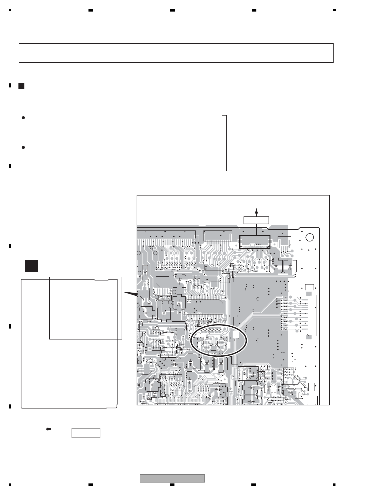
For details, refer to "Important Check Points for good servicing".
STANDBY
PURE AUDIO
ONOFF
PD-D9MK2-K
D9
SUPER AUDIO CD PLAYER
PD-D9MK2-K
THIS MANUAL IS APPLICABLE TO THE FOLLOWING MODEL(S) AND TYPE(S).
Model Type Power Requirement Remarks
PD-D9MK2-K SYXJ5 AC 220 V to 240 V
PD-D9MK2-K CUXJ AC 120 V
ORDER NO.
RRV3939
T- ZZK MAY
2009 Printed in Japan
Page 2
1
NOTICE
(FOR CANADIAN MODEL ONLY )
Fuse symbols (fast operating fuse) and/or (slow operating fuse) on PCB indicate that replacement parts must
be of identical designation.
REMARQUE
(POUR MODÈLE CANADIEN SEULEMENT)
Les symboles de fusible (fusible de type rapide) et/ou (fusible de type lent) sur CCI indiquent que les pièces
de remplacement doivent avoir la même désignation.
This service manual is intended for qualified service technicians; it is not meant for the casual
do-it-yourselfer. Qualified technicians have the necessary test equipment and tools, and have been
trained to properly and safely repair complex products such as those covered by this manual.
Improperly performed repairs can adversely affect the safety and reliability of the product and may
void the warranty. If you are not qualified to perform the repair of this product properly and safely,
you should not risk trying to do so and refer the repair to a qualified service technician.
WARNING
This product may contain a chemical known to the State of California to cause cancer, or birth defects or other reproductive
harm.
Health & Safety Code Section 25249.6 - Proposition 65
ANY MEASUREMENTS NOT WITHIN THE
LIMITS OUTLINED ABOVE ARE INDICATIVE
OF A POTENTIAL SHOCK HAZARD AND
MUST BE CORRECTED BEFORE RETURNING THE APPLIANCE TO THE CUSTOMER.
2. PRODUCT SAFETY NOTICE
Many electrical and mechanical parts in the appliance
have special safety related characteristics. These are
often not evident from visual inspection nor the
protection afforded by them necessarily can be obtained
by using replacement components rated for voltage,
wattage, etc. Replacement parts which have these
special safety characteristics are identified in this
Service Manual.
Electrical components having such features are
identified by marking with a on the schematics and
on the parts list in this Service Manual.
The use of a substitute replacement component which
does not have the same safety characteristics as the
PIONEER recommended replacement one, shown in the
parts list in this Service Manual, may create shock, fire,
or other hazards.
Product Safety is continuously under review and new
instructions are issued from time to time. For the latest
information, always consult the current PIONEER
Service Manual. A subscription to, or additional copies
of, PIONEER Service Manual may be obtained at a
nominal charge from PIONEER.
(FOR USA MODEL ONLY)
1. SAFETY PRECAUTIONS
The following check should be performed for the
continued protection of the customer and service
technician.
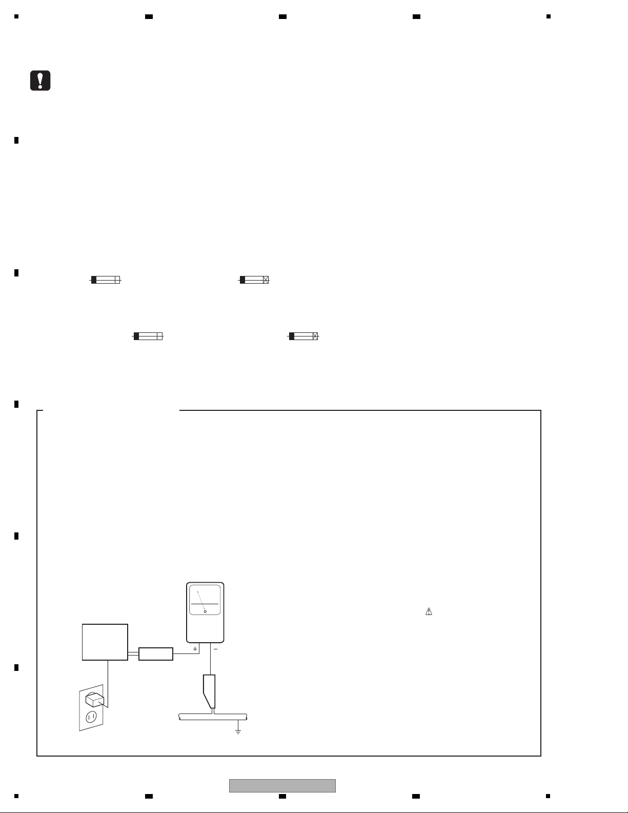
LEAKAGE CURRENT CHECK
Measure leakage current to a known earth ground
(water pipe, conduit, etc.) by connecting a leakage
current tester such as Simpson Model 229-2 or
equivalent between the earth ground and all exposed
metal parts of the appliance (input/output terminals,
screwheads, metal overlays, control shaft, etc.). Plug
the AC line cord of the appliance directly into a 120V
AC 60 Hz outlet and turn the AC power switch on. Any
current measured must not exceed 0.5 mA.
Device
under
test
Leakage
current
tester
Earth
ground
Reading should
not be above
0.5 mA
Also test with
plug reversed
(Using AC adapter
plug as required)
Test al l
exposed metal
surfaces
AC Leakage Test
2 3 4
SAFETY INFORMATION
A
B
C
D
E
F
2
1
2 3 4
PD-D9MK2-K
Page 3
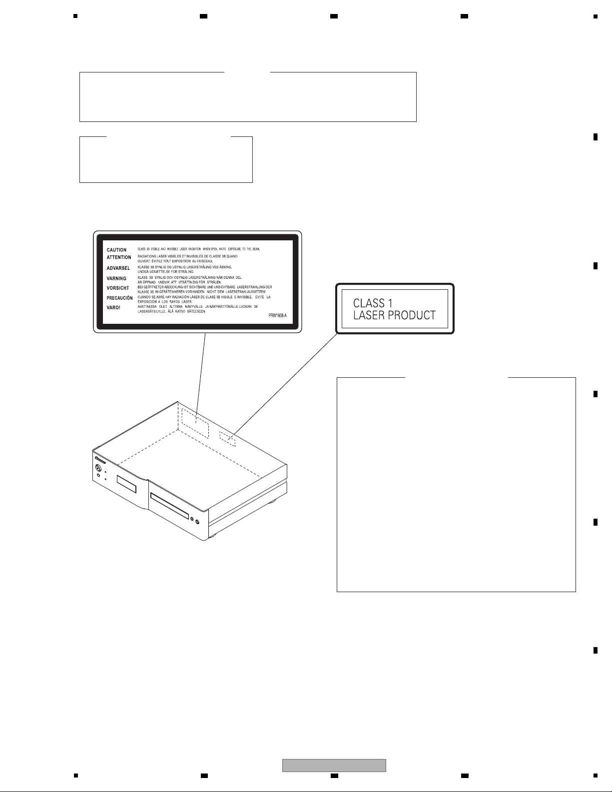
5
WARNING !
THE AEL (ACCESSIBLE EMISSION LEVEL) OF THE LASER POWER OUTPUT IS LESS THAN CLASS 1
BUT THE LASER COMPONENT IS CAPABLE OF EMITTING RADIATION EXCEEDING THE LIMIT FOR
CLASS 1.
A SPECIALLY INSTRUCTED PERSON SHOULD DO SERVICING OPERATION OF THE APPARATUS.
LASER DIODE CHARACTERISTICS
FOR CD : MAXIMUM OUTPUT POWER : 7 mW
WAVELENGTH : 780 nm
FOR SACD : MAXIMUM OUTPUT POWER : 5 mW
WAVELENGTH : 650 nm)
Additional Laser Caution
1. Laser Interlock Mechanism
• Loading switch (S101 on the LOAB Assy) is used for interlock
mechanism of the laser.
When this switch turned ON in SW2 (CLOSE) side (OPEN signal is
0V and CLOSE signal is 3.5V), a laser becomes the status which can
completely oscillation.
Furthermore, the laser completely oscillates in the disc judgment and
disc playback.
When player is power ON state and laser diode is not completely
oscillating, 780nm laser diode is always oscillating by half power.
• Laser diode is driving with Q307 (650nm LD) and Q308 (780nm LD)
on the DVDM Assy.
Therefore, when short-circuit between the emitter and collector of these
transistors or the base voltage is supplied for transistors turn on, the
laser oscillates. (failure mode)
• In the test mode ∗ , there is the mode that the laser oscillates except
for the disc judgment and playback. LD ON mode in the test mode
oscillates with the laser forcibly.
The interlock mechanism mentioned above becomes invalid in this
mode.
2. When the cover is open, close viewing through the objective lens with
the naked eye will cause exposure to the laser beam.
LABEL CHECK
SYXJ5, CUXJ types : PRW1608
(Printed on the Rear Panel )
∗ : Refer to page 38.
6 7 8
A
B
C
D
E
F
PD-D9MK2-K
5
6 7 8
3
Page 4
1
[Important Check Points for Good Servicing]
In this manual, procedures that must be performed during repairs are marked with the below symbol.
Please be sure to confirm and follow these procedures.
1. Product safety
Please conform to product regulations (such as safety and radiation regulations), and maintain a safe servicing environment by
following the safety instructions described in this manual.
1 Use specified parts for repair.
Use genuine parts. Be sure to use important parts for safety.
2 Do not perform modifications without proper instructions.
Please follow the specified safety methods when modification(addition/change of parts) is required due to interferences such as
radio/TV interference and foreign noise.
3 Make sure the soldering of repaired locations is properly performed.
When you solder while repairing, please be sure that there are no cold solder and other debris.
Soldering should be finished with the proper quantity. (Refer to the example)
4 Make sure the screws are tightly fastened.
Please be sure that all screws are fastened, and that there are no loose screws.
5 Make sure each connectors are correctly inserted.
Please be sure that all connectors are inserted, and that there are no imperfect insertion.
6 Make sure the wiring cables are set to their original state.
Please replace the wiring and cables to the original state after repairs.
In addition, be sure that there are no pinched wires, etc.
7 Make sure screws and soldering scraps do not remain inside the product.
Please check that neither solder debris nor screws remain inside the product.
8 There should be no semi-broken wires, scratches, melting, etc. on the coating of the power cord.
Damaged power cords may lead to fire accidents, so please be sure that there are no damages.
If you find a damaged power cord, please exchange it with a suitable one.
9 There should be no spark traces or similar marks on the power plug.
When spark traces or similar marks are found on the power supply plug, please check the connection and advise on secure
connections and suitable usage. Please exchange the power cord if necessary.
a Safe environment should be secured during servicing.
When you perform repairs, please pay attention to static electricity, furniture, household articles, etc. in order to prevent injuries.
Please pay attention to your surroundings and repair safely.
2. Adjustments
To keep the original performance of the products, optimum adjustments and confirmation of characteristics within specification.
Adjustments should be performed in accordance with the procedures/instructions described in this manual.
4. Cleaning
For parts that require cleaning, such as optical pickups, tape deck heads, lenses and mirrors used in projection monitors, proper
cleaning should be performed to restore their performances.
3. Lubricants, Glues, and Replacement parts
Use grease and adhesives that are equal to the specified substance.
Make sure the proper amount is applied.
5. Shipping mode and Shipping screws
To protect products from damages or failures during transit, the shipping mode should be set or the shipping screws should be
installed before shipment. Please be sure to follow this method especially if it is specified in this manual.
A
2 3 4
B
C
D
E
F
4
1
PD-D9MK2-K
2 3 4
Page 5

5
6 7 8
CONTENTS
SAFETY INFORMATION.......................................................................................................................................................... 2
1. SERVICE PRECAUTIONS.................................................................................................................................................... 6
1.1 NOTES ON SOLDERING...............................................................................................................................................6
2. SPECIFICATIONS................................................................................................................................................................. 7
2.1 SPECIFICATIONS .......................................................................................................................................................... 7
2.2 PANEL FACILITIES.........................................................................................................................................................8
3. BASIC ITEMS FOR SERVICE ............................................................................................................................................10
3.1 CHECK POINTS AFTER SERVICING (SACD PLAYER) .............................................................................................10
3.2 PCB LOCATIONS .........................................................................................................................................................11
3.3 JIGS LIST .....................................................................................................................................................................12
4. BLOCK DIAGRAM .............................................................................................................................................................. 14
4.1 OVERALL WIRING DIAGRAM .....................................................................................................................................14
4.2 OVERALL BLOCK DIAGRAM.......................................................................................................................................16
5. DIAGNOSIS ........................................................................................................................................................................18
5.1 TROUBLESHOOTING.................................................................................................................................................. 18
5.2 SEQUENCE AFTER POWER ON/OFF........................................................................................................................ 22
5.3 METHOD FOR DIAGNOSING DEGRADATION OF THE LDS ON THE PICKUP ASSY .............................................26
6. SERVICE MODE................................................................................................................................................................. 27
6.1 TEST MODE.................................................................................................................................................................27
7. DISASSEMBLY ...................................................................................................................................................................28
8. EACH SETTING AND ADJUSTMENT................................................................................................................................ 36
8.1 ADJUSTMENT ITEMS AND LOCATION...................................................................................................................... 36
8.2 JIGS AND MEASURING INSTRUMENTS....................................................................................................................36
8.3 NECESSARY ADJUSTMENT POINTS ........................................................................................................................37
8.4 TEST MODE.................................................................................................................................................................38
8.5 MECHANISM ADJUSTMENT.......................................................................................................................................40
9. EXPLODED VIEWS AND PARTS LIST............................................................................................................................... 42
9.1 PACKING SECTION .....................................................................................................................................................42
9.2 EXTERIOR SECTION .................................................................................................................................................. 44
9.3 CHASSIS SECTION..................................................................................................................................................... 46
9.4 FRONT PANEL SECTION ............................................................................................................................................48
9.5 LOADER ASSY ............................................................................................................................................................50
9.6 TRAVERSE MECHANISM ASSY-S ..............................................................................................................................52
10. SCHEMATIC DIAGRAM.................................................................................................................................................... 54
10.1 DVDM ASSY (1/2) ...................................................................................................................................................... 54
10.2 DVDM ASSY (2/2) ...................................................................................................................................................... 56
10.3 AJKB ASSY ................................................................................................................................................................58
10.4 LCD, PLED, IR and KEY ASSYS................................................................................................................................60
10.5 PRIMARY, MNSW and REGULATOR ASSYS............................................................................................................62
10.6 CONNECTOR ASSY .................................................................................................................................................. 64
10.7 WAVEFORMS.............................................................................................................................................................65
11. PCB CONNECTION DIAGRAM........................................................................................................................................68
11.1 LOAB and DVDM ASSYS ...........................................................................................................................................68
11.2 AJKB ASSY ................................................................................................................................................................70
11.3 LCD ASSY.................................................................................................................................................................. 72
11.4 PLED, KEY and IR ASSYS.........................................................................................................................................74
11.5 PRIMARY ASSY ................................................................................................................
11.6 CONNECTOR and MNSW ASSYS ............................................................................................................................ 78
11.7 REGULATOR ASSY ................................................................................................................................................... 80
12. PCB PARTS LIST.............................................................................................................................................................. 82
......................................... 76
A
B
C
D
E
F
PD-D9MK2-K
5
6 7 8
5
Page 6

1
• For environmental protection, lead-free solder is used on the printed circuit boards mounted in this unit.
Be sure to use lead-free solder and a soldering iron that can meet specifications for use with lead-free solders for repairs
accompanied by reworking of soldering.
• Compared with conventional eutectic solders, lead-free solders have higher melting points, by approximately 40 ºC.
Therefore, for lead-free soldering, the tip temperature of a soldering iron must be set to around 373 ºC in general, although
the temperature depends on the heat capacity of the PC board on which reworking is required and the weight of the tip of
the soldering iron.
Do NOT use a soldering iron whose tip temperature cannot be controlled.
Compared with eutectic solders, lead-free solders have higher bond strengths but slower wetting times and higher melting
temperatures (hard to melt/easy to harden).
The following lead-free solders are available as service parts:
• Parts numbers of lead-free solder:
GYP1006 1.0 in dia.
GYP1007 0.6 in dia.
GYP1008 0.3 in dia.
2 3 4
1. SERVICE PRECAUTIONS
1.1 NOTES ON SOLDERING
A
B
C
D
E
F
6
1
2 3 4
PD-D9MK2-K
Page 7
5
Accessories
Remote control . . . . . . . . . . . . . . . . . . . . . . . . . . 1
AAA/IEC R03 dry cell batteries . . . . . . . . . . . . 2
RCA/phono stereo audio cable . . . . . . . . . . . . . 1
SR control cable . . . . . . . . . . . . . . . . . . . . . . . . . 1
Power cable . . . . . . . . . . . . . . . . . . . . . . . . . . . . . 1
Warranty card
Operating Instructions
Note
• Specifications and the design are subject
to possible modifications without notice,
due to improvements.
Specifications
General
System . . . . . . . . . . . . . . . Super Audio CD player
Power requirements . . . . . . . . . . . . . . . . .
SYXJ5: AC 220 V to AC 240 V, 50/60 Hz
CUXJ: AC 120 V, 60 Hz
Power consumption . . . . . . . . . . . . . . . . . . . .22 W
Power consumption (standby) . . . . . . . . . . . 0.4 W
Weight. . . . . . . . . . . . . . . . . . . . 11.0 kg (24 lbs 5oz)
Dimensions
. . . . . . . .420 mm (W) x 113 mm (H) x 340 mm (D)
(16
9
/16 in. (W) x 4 1/2 in. (H) x 13 3/8 in. (D))
Operating temperature . . . . . . . . +5 °C to +35 °C
Operating humidity . . . . . . . . . . . . . . . 5 % to 85 %
(no condensation)
Audio output (1 stereo pair)
Output level . . . . . . . . . . . . . .During audio output
200 mVrms (1 kHz, –20 dB)
Number of channels . . . . . . . . . . . . . . . . . . . . . . . 2
Jacks . . . . . . . . . . . . . . . . . . . . . . . . . . . . . . . . . RCA
Digital audio characteristics
Frequency response . . . . . 4 Hz to 50 kHz (SACD)
4 Hz to 20 kHz (CD)
S/N ratio:
CD . . . . . . . . . . . . . . . . . . . . . . . . . . . . . . . 115 dB
SACD . . . . . . . . . . . . . . . . . . . . . . . . . . . . 110 dB
Dynamic range:
CD . . . . . . . . . . . . . . . . . . . . . . . . . . . . . . . 100 dB
SACD . . . . . . . . . . . . . . . . . . . . . . . . . . . . 110 dB
Total harmonic distortion:
CD . . . . . . . . . . . . . . . . . . . . . . . . . . . . . . 0.002 %
SACD . . . . . . . . . . . . . . . . . . . . . . . . . . . 0.003 %
Wow and flutter . . . . . . . . . Limit of measurement
(±0.001 % W. PEAK) or lower
Digital output
Coaxial digital output. . . . . . . . . . . . . . . RCA jack
Optical digital output. . . . . . . Optical digital jack
Disc/content format playback
compatibility
This player is compatible with a wide range of
audio disc types and media formats. Playable
discs will generally feature one of the following
logos on the disc and/or disc packaging. Note
however that some disc types, such as
recordable CDs, may be in an unplayable
format.
Please also note that recordable discs cannot be
recorded using this player.
*“Super Audio CD” is a registered trademark.
Audio CD CD-R CD-RW
Super Audio CD*
2. SPECIFICATIONS
2.1 SPECIFICATIONS
6 7 8
A
B
C
D
E
5
PD-D9MK2-K
6 7 8
F
7
Page 8
1
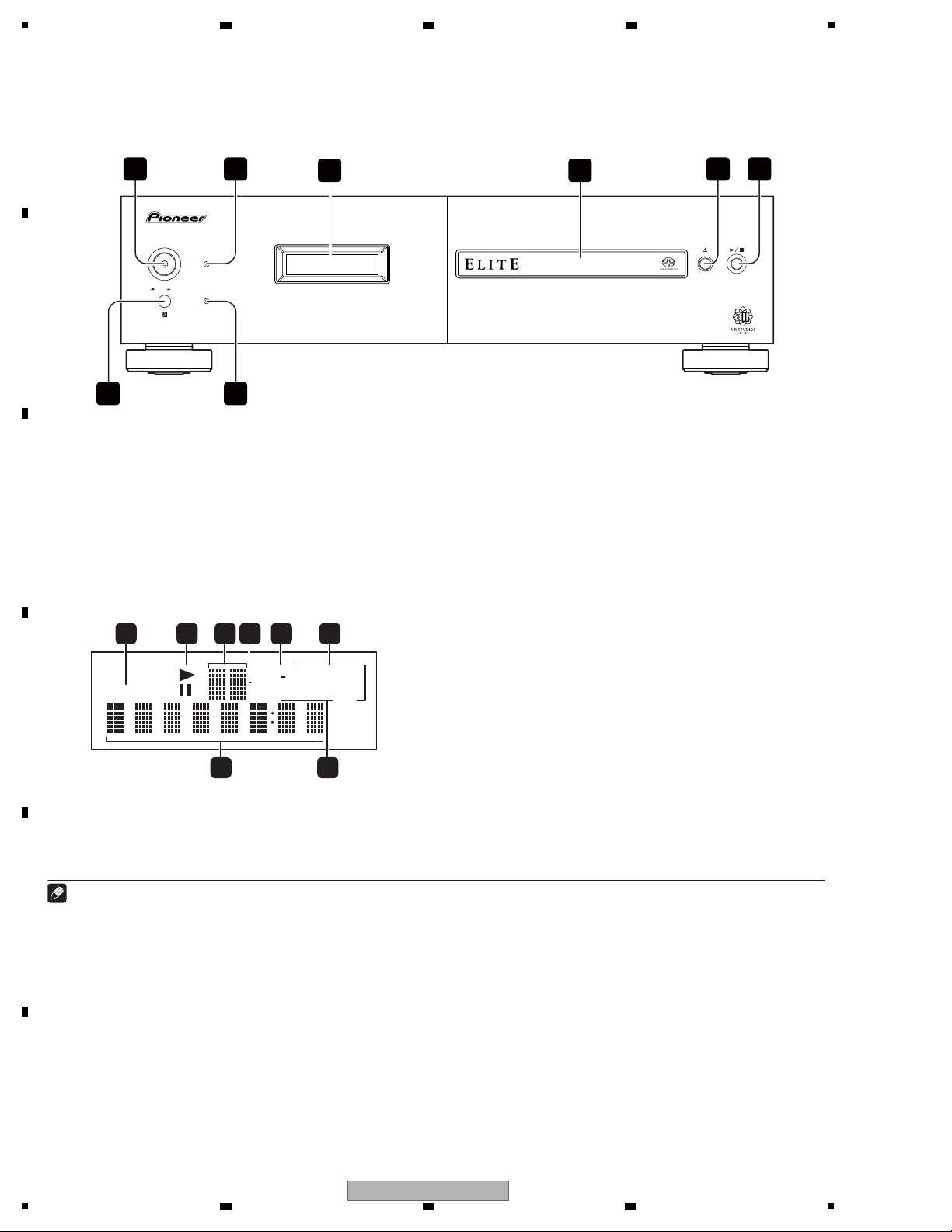
Front panel
1
POWER v
OFF wON
1
2 STANDBY indicator
3 Display
(below)
4 Disc tray
5 h
6 d/g
7 Remote sensor
8
PURE AUDIO
indicator
Display
1
TRACK – Lights when the track number is
indicated.
2
d/e – Light during playback/when paused.
3Scan display
– Shows the scan speed.
4 SACD – Lights during SACD playback.
5
LEGATO – Lights when Legato Link Pro is
switched on.
6(ALL)
REPEAT/RANDOM/PGM – Light to
indicate the playback mode.
7 Character display
8 TOTAL/REMAIN
–
Indicate the disc/track
information currently displayed.
ONOFF
POWER
STANDBY
PURE AUDIO
D9
3 4
1
7
2 5 6
8
Note
1 • When the unit is in the standby mode, if the power is turned off by pressing the main unit’s POWER button, the power will
not turn on if the button is pressed again. To turn on the power in this case, press either the remote control unit’s
CD PLAYER u button or a different button (other than the POWER button) on the main unit.
• When the unit is in the standby mode, if the power is turned off by unplugging the power cord, the power will not turn merely
by reconnecting the power cord. To turn on the power in this case, reconnect the power cord and then press either the remote
control unit’s CD PLAYER u button or a different button (other than the POWER button) on the main unit.
LEGATOLEGATO
ALLALL
TOTALTOTAL
REPEATREPEAT
PGMPGM
REMAINREMAIN
RANDOMRANDOM
TRACKTRACK
SACDSACD
1 2 3 4 5 6
7 8
2.2 PANEL FACILITIES
A
B
2 3 4
C
D
E
8
1
PD-D9MK2-K
2 3 4
F
Page 9
5
Remote control
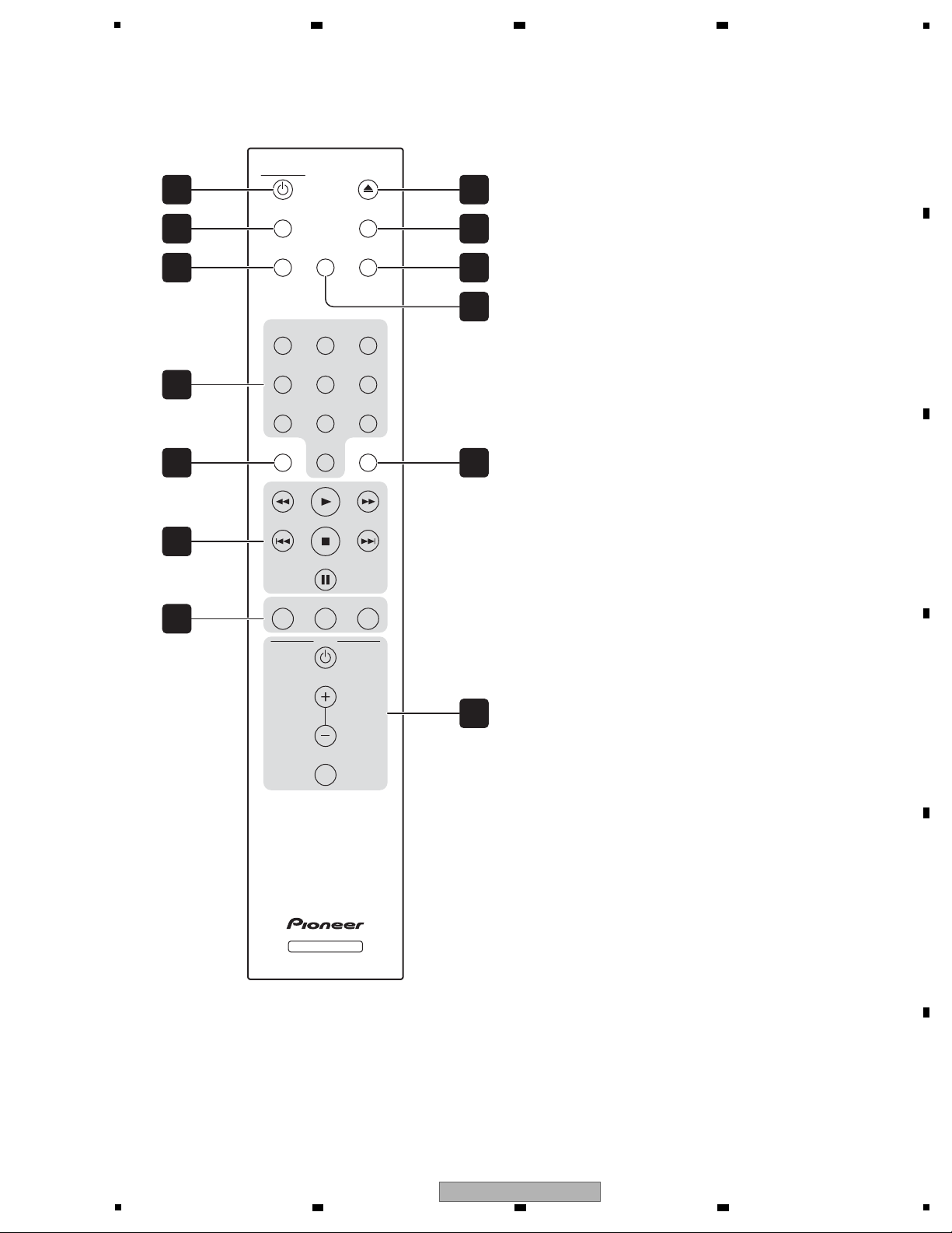
1
CD PLAYER u
2
TIME
3
SACD/CD
4 Number buttons
5
CLEAR
6 Playback controls
7
PROGRAM
REPEAT
RANDOM
8
h OPEN/CLOSE
9
DIMMER
10
PURE AUDIO
11
LEGATO LINK
12
ENTER
13 AMP controls
Use to control Pioneer amplifier.
AMP u
VOLUME
MUTE
PROGRAM
REPEAT
VOLUME
RANDOM
AMP
SACD PLAYER
CD PLAYER
OPEN/CLOSE
TIME
DIMMER
SACD/CD
PURE AUDIO
CLEAR ENTER
LEGATO
LINK
123
456
7809
MUTE
1 8
9
10
12
13
11
2
3
4
6
7
5
6 7 8
A
B
C
D
5
PD-D9MK2-K
6 7 8
E
F
9
Page 10
1
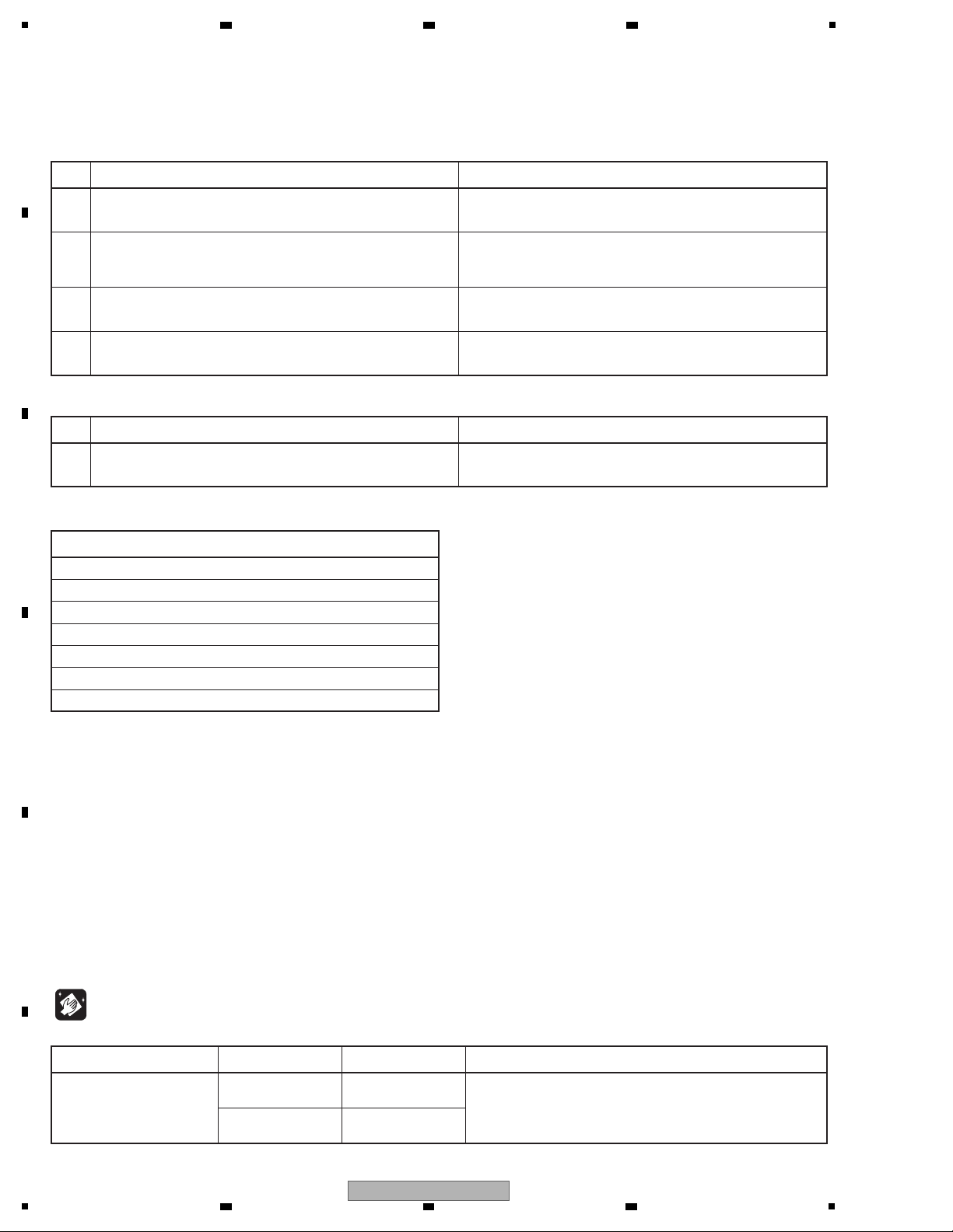
Item to be checked regarding audio
Distortion
Noise
Volume too low
Volume too high
Volume fluctuating
Sound interrupted
No. Procedures Check points
1
2
3
4
Confirm the firmware version on Test Mode. The version of the firmware must be latest.
Update firmware to the latest one, if it is not the latest.
Confirm whether the customer complain has been solved.
If the customer complain occurs with the specific disc, use it for
the operation check.
The customer complain must not be reappeared.
Video, audio and operations must be normal.
Play back a CD.
(track search)
Audio and operations must be normal.
Check the appearance of the product. No scratches or dirt on its appearance after receiving it for
service.
Items to be checked after servicing / PD
To keep the product quality after servicing, confirm recommended check points shown below.
See the table below for the items to be checked regarding audio.
Cleaning
Before shipping out the product, be sure to clean the following positions by using the prescribed cleaning tools.
NamePosition to be cleaned Part No. Remarks
Refer to “9.6 Traverse Mechanism Assy-S”.Cleaning liquidPickup leneses GEM1004
Cleaning paper GED-008
No. Procedures Check points
1
Play back a SACD. *Models supporting SACD
(track search)
Audio and operations must be normal.
Specific Items to be Checked
2 3 4
3. BASIC ITEMS FOR SERVICE
3.1 CHECK POINTS AFTER SERVICING (SACD PLAYER)
A
B
C
D
E
F
10
1
2 3 4
PD-D9MK2-K
Page 11
5
REGULATOR ASSY
J
AJKB ASSY
C
CONNECTOR
ASSY
H
KEY ASSY
G
LOAB ASSY
A
LCD ASSY
D
PLED ASSY
E
IR ASSY
K
MNSW ASSY
F
PRIMARY ASSY
I
DVDM ASSY
B
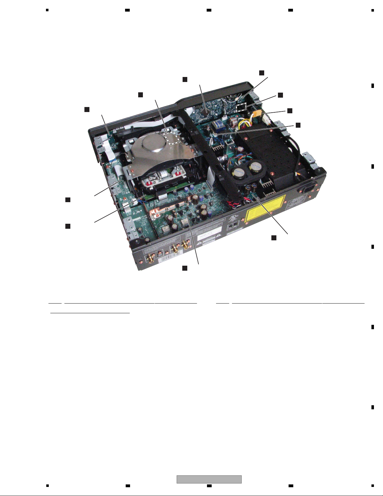
3.2 PCB LOCATIONS
6 7 8
A
B
Mark No. Description Part No.
LIST OF ASSEMBLIES
For PD-D9MK2-K/SYXJ5
NSP 1..LOADER ASSY PXA1648
NSP 2..LOAB ASSY VWG2346
1..DVDM ASSY AWM8184
1..FLKB ASSY PWM2371
2..IR ASSY(D9) PWX1653
2..MNSW ASSY(D9) PWX1654
2..LCD ASSY(D9) PWX1672
2..PLED ASSY(D9) PWX1677
2..KEY ASSY(D9) PWX1679
2..REGULATOR ASSY(D9) PWX1678
2..PRIMARY ASSY(D9 WY) PWX1681
1..AJKB ASSY PWM2375
2..AJKB ASSY(D9) PWX1685
2..CONNECTOR ASSY(D9) PWX1686
Mark No. Description Part No.
For PD-D9MK2-K/CUXJ
NSP 1..LOADER ASSY PXA1648
NSP 2..LOAB ASSY VWG2346
1..DVDM ASSY AWM8184
1..FLKB ASSY PWM2373
2..IR ASSY(D9) PWX1653
2..MNSW ASSY(D9) PWX1654
2..LCD ASSY(D9) PWX1672
2..PLED ASSY(D9) PWX1677
2..KEY ASSY(D9) PWX1679
2..REGULATOR ASSY(LOW) PWX1680
2..PRIMARY ASSY(D9 KU) PWX1683
1..AJKB ASSY PWM2375
2..AJKB ASSY(D9) PWX1685
2..CONNECTOR ASSY(D9) PWX1686
C
D
E
F
PD-D9MK2-K
5
6 7 8
11
Page 12
1
Service Remote Control Unit GGF1381
DVD Test Disc (DVD-Video) GGV1025
adjustment, diagnosis
Name Jig No. Remarks
Check of DVD-Video
CD Test Disc STD-905 Check of CD
5P FFC GGD1425 Diagnosis of DVDM ASSY
17P FFC GGF1157 Diagnosis of DVDM ASSY
Jigs list
Silicone Adhesive GYA1011
refer to "9.4 FRONT PANEL SECTION"
Lubricating Oil GYA1001
GEM1036
Daifree
Name Lubricants and Glues No. Remarks
refer to "9.5 LOADER ASSY"
refer to "9.5 LOADER ASSY"
GEM1037Silicone Adhesive
refer to "9.6 TRAVERSE MECHANISM ASSY-S"
GYL1001Screw tight
refer to "8.5 MECHANISM ADJUSTMENT"
Lubricants and Glues list
2 3 4
3.3 JIGS LIST
A
B
C
D
E
F
12
PD-D9MK2-K
1
2 3 4
Page 13

5
6 7 8
A
B
C
D
E
F
PD-D9MK2-K
5
6 7 8
13
Page 14
1
AJKB ASSY
(PWX1685)
C
LCD ASSY
(PWX1672)
D
PLED ASSY
(PWX1677)
E
IR ASSY
(PWX1653)
K
MNSW ASSY
(PWX1654)
F
PRIMARY ASSY
(PD-D9MK2-K/SYXJ5:
PWX1681)
(PD-D9MK2-K/CUXJ:
PWX1683)
I
REGULATOR ASSY
(PD-D9MK2-K/SYXJ5: PWX1678)
(PD-D9MK2-K/CUXJ:PWX1680)
J
SYXJ5: ADG7062
CUXJ: ADG7061
SYXJ5: PTT1372
CUXJ: PTT1371
SYXJ5: PTT1374
CUXJ: PTT1373
2 3 4
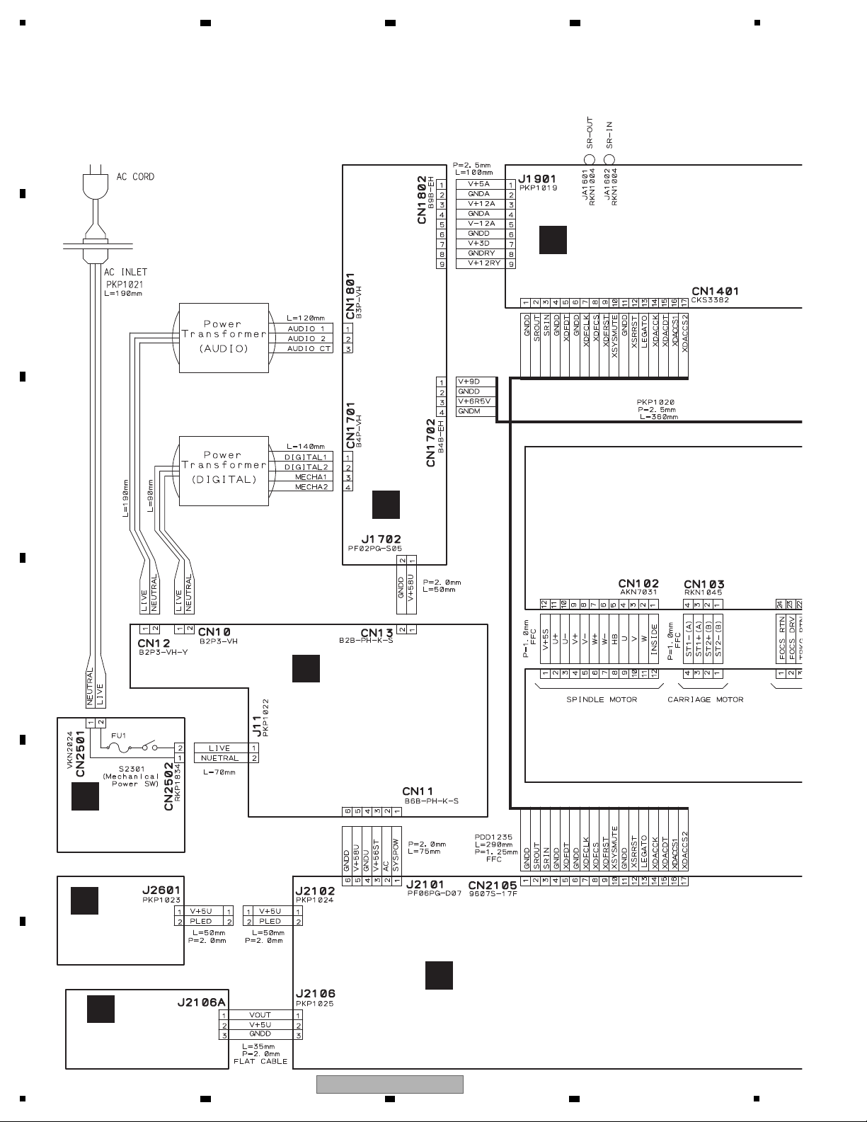
4. BLOCK DIAGRAM
4.1 OVERALL WIRING DIAGRAM
A
B
C
D
E
F
14
PD-D9MK2-K
1
2 3 4
Page 15
5
V+3D
SW2
LOAD+
LOAD-
SW1
S5B-PH-K-S
CN601
CN602
LOADING
MOTOR
ASSY
: VXX2912
1
2
DVDM ASSY
(AWM8184)
CONNECTOR ASSY
(PWX1686)
H
KEY ASSY
(PWX1679)
G
LOAB ASSY
(VWG2346)
A
MECHA ASSY
B
B
()
1/2,B2/2
6 7 8
A
B
C
D
E
F
PD-D9MK2-K
5
6 7 8
15
Page 16
1
CN101
CN953
CN901(1/2)
CN2105
J2104
CN1401
J2106
J2104A
CN901(2/2)
CN2106
J2106A
CN103
CN102
CN104
IC201
MAIN DECODER
(CD,SACD)
1389EE
3.3V&1.8V
64M SDRAM
IC202
KS641632H-TC75
3.3V
IC203
PGM FLASH MEMORY
16M
AYW7197
3.3V
EEPROM
IC204
4k
3.3V
S-24C04AFJ
LOADING
MOTOR
SPDL
MOTOR
PU
STEPPING
MOTOR
TRAVERSE
05 PICK
UP
IC101
SERVO
DRIVER
BD7995EFS
6.5&5V
IC2101
SYSTEM
CONTROL
CPU
5V
PDC170B
LCD Display
AAV7118
5V
KEY
S2301, S2302
IR
GP1UM28XK
5V
Front Panel Block
X202
Clock OSC
ASS7103
(27MHz)
3.3V
SPDIF
DVDM ASSY
B
LCD ASSY
D
KEY ASSY
G
IR ASSY
K
2 3 4
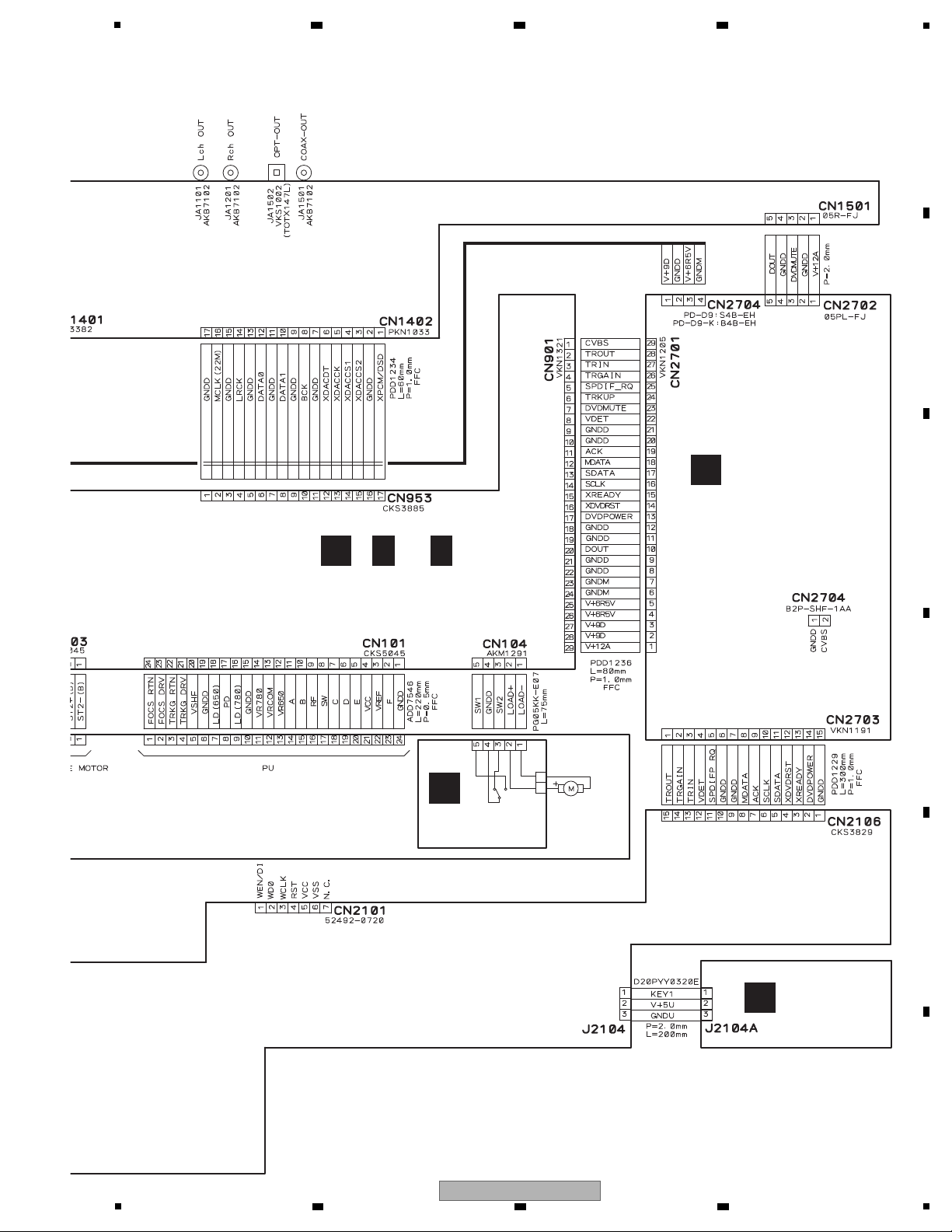
4.2 OVERALL BLOCK DIAGRAM
A
B
C
D
E
F
16
1
2 3 4
PD-D9MK2-K
Page 17
CN1402
CN1501
CN1401
OPTICAL OUT
COAXIAL OUT
SR-IN
SR-OUT
L
R
JA1101
JA1201
JA1502
JA1501
JA1602
JA1601
LPF
IC1101
(1/2)
IC1101
(2/2)
IC1201
(2/2)
IC1201
(1/2)
(PCM)
IC1401
AQE
PD0274A
3.3V
(DSD)
MCLK
IC1251
IC1151
192k,24bit,
2chDAC
WM8741
3.3V&5V
192k,24bit,
2chDAC
WM8741
3.3V&5V
SEL
SEL
IC1152
IC1252
IC1402
SRC
SRC4192
3.3V
X1401
Clock OSC
ASS7101
(22MHz)
3.3V
MCLK
AJKB ASSY
C
5
6 7 8
A
B
C
D
E
F
PD-D9MK2-K
5
6 7 8
17
Page 18
1
Start
(Power → ON)
Lighting LCD
come out of the pure audio
mode or dimmer mode
Refer to Addendum No. 1.
Appearance some waveform on
LCD communication line
(LCCDT,LCDCK,LCDCS,LCDRS)
Confirm the port logic of BLOFF
and DIMMER when operate
Confirmation HB at CN1801or change
D1801,D1802,D1803D1804
<confirmation>
FU1
Connection between J1702 and CN13
Power line CN11 3 : 5.6V,CN11 5 : 5.8V
<confirmation>
D1809 is shorten
HB at CN1802 and J1901
CN1802 3 is +13V
Ye s
Ye s
No
No
No
<confirmation>
input and output of F2201,Q2103 is 5V
Ye s
No
No
LCD
displays
correctly
V2201 1
is 4.4V and
V2201 2 is
5V
Ye s
No
Tray movement
(open/close)
Refer to Addendum No. 2.
Ye s
No
Focus
movement
OK?
Refer to Addendum No. 3.
Ye s
No
Spindle
movement
OK?
Refer to Addendum No. 4.
Ye s
No
Can stop
spicdle movement
(stop key react)
Ye s
No
<confirmation>
Connection between CN1802 and J1901
Connection between CN1501 and CN2702
Connection between CN2701 and CN901
Connection between CN1702 and CN2704
Ye s
Ye s
Ye s
No
No
Change parts D1805,Q1801,
Q1802 in turn
Change parts D1807,Q1803,
in turn
No
<confirmation>
HB at IC1101,IC1201
No
(V+3D line)
CN1802 3
is 3.3V
<confirmation>
HB at J1901,CN1802,
IC1151,IC1152,IC1251,IC1252,
IC1401-IC1406
No
Ye s
<confirmation>
HB at CN1701
Change IC1701
No
LCD
disappers and
flashing pure
audio LED
(V+12V line)
Cathode of 1801,
D1802 is
+17V
(V+5V line)
CN1802 1 is +5V
Ye s
No
(V+9D line)
D1701 1 is +7.5V
Is status of
IC1701 OK?
Ye s
<confirmation>
HB at CN1701
Change IC1702
No
No
Is status of
IC1702 OK?
CN1702 3
is +6.5V
<confirmation>
HB at CN1702,CN2704,IC101
No
Ye s
(V+6R5V line)
D1702 1
is +8.5V
A
Working
at pure audio
mode or
dimmer?
5. DIAGNOSIS
5.1 TROUBLESHOOTING
A
2 3 4
B
C
D
E
F
18
PD-D9MK2-K
1
2 3 4
Page 19
no ploblem
<confirmation>
HB of CN1801
CN1802 is -13V
Change parts
D1808,Q1804,
in turn
Ye s
No
Audio
analog output
is OK?
only analog output at
SACD mode
All output
audio signal
are OK?
Ye s
Only
optical or coaxial
output
Ye s
Ye s
No
<confirmation>
IC201-225
Connection between CN953and CN1402
<confirmation>
Input and output of IC1501
V+3DO is 3.3V
Ye s
RY1302 a
is 0V
Ye s
Ye s
No
Change parts D1806,
Q1804,Q1805 in turn
Ye s
<confirmation>
HB at IC1101,IC1201
Ye s
Change RY1302
No
<confirmation>
XSYSMUTE : H
DVDMUTE : L
<confirmation>
HB at CN1701 or
change D1709,D1710
No
IC1707 1 is
+17V
Ye s
Change IC1707
No
status of IC1706
is OK?
Ye s
Change IC1706
No
No
(V+12RY line)
RY1302 1 is
+12V
NoNo
(V-12V line)
anode of D1803,
D1804 is -17V
A
5
6 7 8
A
B
C
D
5
PD-D9MK2-K
6 7 8
E
F
19
Page 20
1
No. Symptoms Diagnosis Contents Possible Defective Points
1 The power is not turned on. Are wires of output connector (POWER SUPPLY Unit) and CN901
(DVDM Assy) disconnected or damaged ?
Connector / cable
Check that the following voltage is output :
+ side of C739 : 3.3V
DVDM Assy
3.3V Regulator IC (IC341)
2
An opening screen is not
displayed on the monitor
(The FL display lights. The
mechanism does not work.)
Are the signals output from IC201-pin 98 (MDATA) and pin 99 (SCLK)
on the DVDM Assy ? (in the range of 0-3V)
DVDM Assy
DVD IC (IC201)
Are the signals input into IC2101-pin 50 (MDATA) and pin 51 (SCLK) on
the LCD Assy ? (in the range of 0-3V)
LCD Assy
UCOM (IC2101)
Check that the following voltage are output :
IC751-pin 1 on the DVDM Assy : 5V
DVDM Assy
5V Regulator IC (IC751)
Is a resonator (X202: 27MHz) on the DVDM Assy oscillating ?
DVDM Assy
Crystal resonator (X202)
• Is a signal input into IC203-pin26 (PCE#) on the DVDM Assy ?
(Is a signal "H" for 80 mS and then "L" after the power is turned
on ?)
→ Communication with flash ROM.
• Are the signals input into IC202-pin 16 (DWE#), pin 19 (DCS#)
and pin 38 (SDCLK) on the DVDM Assy ?
(Is a signal fluctuating ?)
→ Communication with SDRAM
DVDM Assy
DVD IC (IC201)
Flash ROM (IC203)
SDRAM (IC202)
Is a signal output from IC203-pin 28 (PRD#) on the DVDM Assy?
(Is a signal fluctuating for several hundred mS after the power is turned
on ?)
DVDM Assy
Flash ROM (IC203)
Is a signal input into IC2101-pin 67 (DVD ACK) on the LCD Assy ?
(Is a signal fluctuating ?)
→ Communication with FL Control IC
DVDM Assy
DVD IC (IC201)
LCD Assy
UCOM (IC2101)
Is a signal output from IC2101-pin 30 (XREADY) on the LCD Assy ? (Is
a signal fluctuating in the range of 0-5V ?)
LCD Assy
UCOM (IC2101)
Are the signals output from IC2101-pin 49 (SDATA) on the LCD Assy ?
(in the range of 0-5V)
DVDM Assy
DVD IC (IC201)
LCD Assy
UCOM (IC2101)
Are the signals of IC204-pin 5(SDA) and pin 6(SCL) on the DVDM Assy
fluctuating for one or two seconds after the power is turned ?
DVDM Assy
EEPROM (IC204)
Addendum No.1
3
A tray cannot be opened.
(An opening screen is
displayed on the monitor)
LOAB Assy
Tray SW (S101)
Is the signal input into IC101-pin 11 (TROPEN) on the DVDM Assy ?
At open: 3.3V, At close: 0V
DVDM Assy
DVD IC (IC201)
Are the signals output from IC101-pin 1 and pin 2 (CN103-pin 1 and
pin 2) on the DVDM Assy ?
Pin 2: Approx. 6V during opening tray approx. 0V during closing tray.
Pin 1: Approx. 0V during opening tray approx. 6V during closing tray.
DVDM Assy
FTS Driver IC (IC101)
Are wires of CN104 and CN103 on the DVDM Assy disconnected or
damaged ?
Connector / cable
Does the voltage of CN102-pin 1 on the DVDM Assy change to 0V by
pressing the Inside switch.
Inside switch
Does the voltage of CN104-pin 3 and pin 5 on the DVDM Assy change
normally ?
Pin 3 (SW2(TRIN)): Tray is fully closed: "L"
Pin 5 (SW1(TROUT)): Tray is fully opened: "L"
A
2 3 4
B
C
D
E
F
20
1
PD-D9MK2-K
2 3 4
Page 21
5
No. Symptoms Diagnosis Contents Possible Defective Points
4
Playback impossible
(no focusing)
Are the signals output from IC101-pin 3 (FOCS_DRV) and pin 4
(FOCS_RTN) on the DVDM Assy ?
DVDM Assy
FTS Driver IC (IC101)
Does 650-nm LD emit light ?
Does a pickup lens move up / down ?
Does an actuator spring bend ?
Pickup
Are plastic parts damaged ? Or is a shaft detached ?
Is the turntable detached or tilted ?
Mechanism section (motor)
Is flexible cable of CN101 on the DVDM Assy disconnected or
damaged ?
Flexible cable / connector
Is signal output from IC201-pin 42 (FOSO) on the DVDM Assy ?
(Device control of about 1.4 V is output usually. It is fluctuated by about
250 mV with focus up / down.)
DVDM Assy
DVD IC (IC201)
5
Playback impossible
(Spindle does not turn)
Are the signals output from IC101-pin 30 (W), pin 33 (V) and pin 35 (U)
on the DVDM Assy ?
Is pin 26 (STBY) fixed LOW ? (pin 26 is High at playback: 3V)
DVDM Assy
FTS Driver IC (IC101)
Is there any part detached from the spindle motor ?
Or Is there any foreign object lodged in it ?
Mechanism section
(Spindle motor)
Are wires of CN102 on the DVDM Assy disconnected or damaged ? Flexible cable / connector
Is signal output from IC201-pin 37 (DMSO) on the DVDM Assy ?
DVDM Assy
DVD IC (IC201)
6
Playback impossible
(Playback stops)
Does 650-nm LD deteriorate ?
If the voltage at each both ends of R322 and R325 on the DVDM Assy
is 0.4 V or more, the 650-nm LD is definitely deteriorated.
650-nm LD deteriorated.
(When playback of a DVD is
impossible)
Does 780-nm LD deteriorate ?
If the voltage at each both ends of R321 and R326 on the DVDM Assy
is 0.4 V or more, the 780-nm LD is definitely deteriorated.
780-nm LD deteriorated.
(When playback of a CD is
impossible)
Is there abnormality in FG waveform ? (IC201-pin 47)
DVDM Assy
FG output : FTS Driver IC (IC101)
Are there scratches or dirt on the disc ? Disc
Addendum No.2
Addendum No.4
Addendum No.3
6 7 8
A
B
C
D
E
F
PD-D9MK2-K
5
6 7 8
21
Page 22
1
Set time for the current step Elapsed time Details on control
0 msec
POWER ON start, Various initial settings 1
All keys are masked.
XSYSMUTE ON
+ 60 msec 60 msec
Various initial settings 2
SYSPOW ON
When the power is turned on, the HELLO display is requested (3.5 sec).
+ 240 msec 300 msec
Various initial settings 3
RESET L ⇒ H
+ 60 msec 360 msec
Various initial settings 4
Control of the LCD driver starts.
Data transmission
Various initial settings 5
SRC reset
RESET L ⇒ H
+ 240 msec 600 msec
+ 120 msec 1890 msec
Various initial settings 9
Masking of all keys is canceled.
+ 390 msec 1770 msec
Various initial settings 8
+ 480 msec 1380 msec
Various initial settings 7
Bus communication starts.
+ 300 msec 900 msec
Various initial settings 6
DAC setting
+ 3120 msec 5010 msec
Various initial settings a
Temporary data transmission
+ 30 msec 5040 msec
POWER ON completed
Normal POWER-ON sequences
Normal POWER-OFF sequences
Set time for the current step Elapsed time Details on control
0 msec
POWER OFF start, Various settings 1
The mask flags for all keys are set.
+ 30 msec 30 msec
(Note 1)
Various settings 2
Whether the DVD is turned power-off or not is checked.
Bus communication is terminated.
+ 120 msec 150 msec
Various settings 3
+ 330 msec 480 msec
Various settings 4
+ 1320 msec 1800 msec
Various settings 4
All the indications on the LCD are deleted.
Various settings 5
Bus communication is terminated.
+ 90 msec 1890 msec
+ 240 msec 2130 msec Processing for the ports required when the power is turned off
+ 30 msec 2160 msec
POWER OFF completed
(passes every loop in the POWER OFF)
Note 1: In this step, the unit wait for the DVD module to turn the power off. If the DVD module takes a longer time to turn itself off,
the elapsed time will become longer, by just that much.
2 3 4
5.2 SEQUENCE AFTER POWER ON/OFF
A
B
C
D
E
F
22
1
PD-D9MK2-K
2 3 4
Page 23
5
Display only POWER-ON sequences
Display only POWER-OFF sequences
Set time for the current step Elapsed time Details on control
0 msec
Display only POWER ON start, Various initial settings 1
Masking of all keys is canceled.
The normal operation keys are masked.
POWER MUTE ON
SYSTEM POWER1 ON (Pin 91: H)
+ 60 msec 60 msec
Various initial settings 2
+ 240 msec 300 msec
Various initial settings 3
Switched 5 V ON completed (power supply is stabilized)
Masking of the normal operation keys is canceled.
SYSTEM POWER2 ON (Pin 92: H)
+ 60 msec 360 msec
Various initial settings 4
Power-on of the LCD driver starts.
+ 330 msec 690 msec
Display Only POWER ON completed
Set time for the current step Elapsed time Details on control
0 msec
Display only POWER OFF start, Various settings 1
• The mask flags for all the keys are set.
• The mask flags for the normal operation keys are set.
• Muting the power system (SYSTEM MUTE REQUEST)
• Power-off of the LCD driver starts.
+ 4120 msec 4120 msec
Various settings 2
+ 120 msec 4240 msec
Various settings 3
+ 760 msec 5000 msec
Various settings 4
• Masking of all keys is canceled.
• Muting of the power system is canceled.
• Other than in an emergency power-off, the unit awaits for a while.
• SYSTEM POWER2 OFF (Pin 92: H)
+ 240 msec 5240 msec
Display only POWER OFF completed
• SYSTEM POWER1 OFF (Pin 91: H)
6 7 8
A
B
C
D
E
5
PD-D9MK2-K
6 7 8
F
23
Page 24
1
POWER-ON timing waveform
300 600 900 1200 1500 1800 2100 2400 2700 4800 5100
SYSTEM
ok SYSPOW
(41pin )
ok XSYSMUTE
(38pin)
DVD control
DVD ON/OFF
XDVD RESET
ok SYSTEM BUS
(DVD)
SRC control
XSRCRST
(79pin)
DAC control
XDACCLK (65pin)
XDACDT (64pin)
XDACCS1 (63pin)
XDACCS2 (62pin)
LCD control
ok LCD setting
ok LCD reset
others
Subsequently, H or L is output, as appropriate.
(Port setting)
Other output port
PON4
600msec300msec 360msec
1 Standby → On
PON1
60msec
KEY input
0msec
PON2 PON3
PON5
900msec 1380msec 1770msec 1890msec 5010msec
PON6
PON9
5040msec
PON10
Mute cancel
PON7 PON8
A
2 3 4
B
C
D
E
F
24
1
2 3 4
PD-D9MK2-K
Page 25
5
SYSTEM
DVD control
LCD control
Others
POWER-OFF timing waveform
300 600 900 1200 1500 1800 2100 2400 2700 3000 3300 3600 3900 4200 4500 4800
SYSPOW
(41pin )
XSYSMUTE
(38pin)
DVD ON/OFF
(1pin/DVD ON/OFF)
XDVDRESET
(93pin/XDVDRST)
SYSTEM BUS(DVD)
(30,49,50,51,67pin)
LCD setting
(26,27,28pin)
LCD reset
(36pin/XLCDRST)
XDimmer
(70pin/DIMMER)
POFF4
2 On → Standby
POFF1
30msec
150msec 480msec 1800msec 1890msec 2130msec
POFFGO
0msec
POFF2 POFF3
POFF5 POFF6
6 7 8
A
B
C
D
E
5
PD-D9MK2-K
6 7 8
F
25
Page 26
1
DVDM ASSY
B
SIDE A
Front side
D
Q
Q
0
9
2
V
5
R326
R325
R322
R321
Case when this diagnosis is required :
When playback of any disc, including a test disc (DVD: GGV1025, CD: STD-905), won't play or doesn't play
How to diagnose
In the case mentioned above, degradation of the laser diodes (LDs) mounted on the 05SD Pickup Assy is suspected.
Measure the voltage between the two ends of one of the resistors mentioned below.
If the measurements show degradation
of an LD, replace the 05SD Pickup Assy.
Measure the voltage between the both ends of R322 or R325 on the DVDM
Assy. If the voltage is 0.4 V or higher, the 650-nm LD is degraded.
No playback of a DVD (Test Mode), No playback of a SACD :
Measure the voltage between the both ends of R321 or R326 on the DVDM
Assy. If the voltage is 0.4 V or higher, the 780-nm LD is degraded.
No playback of a CD :
05SD PICKUP ASSY
CN101
2 3 4
5.3 METHOD FOR DIAGNOSING DEGRADATION OF THE LDS ON THE PICKUP ASSY
A
B
C
UP SIDE
GNDD
8V
R904
R901
Q702
C1002
D751
IC761
R751
C751
5
D
E
7
R761
E
1
4
5
L751
C752
R750
C
R736
13
R734
R737
R712
R713
C712
3.3V
5
4
R714
1
8
IC711
C221
C713
64
R2
6
CN901
R906
R762
GNDM
6.5V
C761
C132
C131
C145
C144
C146
D881
Q881
Q801
C206
A
C801
R214
C204
D
12
C140
1
R154
R152
R907
R905
R903
C104
C101
R153
R151
22
C161
C143
LD_CD
R134
R132
R131
R321
D801
C203
R801
3.3V
C215
C344
C346
C345
C347
C213
R207
1
R918
C310
C343
R910
25
R911
R919
L309
R912
C103
C151
CN102
R913
R914
1
IC101
R314
R915
C152
C153
C102
L308
BOTTOM SIDE
1
Q304
R136
R133
R135
C141
C142
C133
Q308
R325
R326
LD_DVD
R322
Q307
3.3V
C320
R310
C309
C505
C506
R594
R502
R595
C202
R5
R315
R318
R313
24
31
C503
C502
54
Q305
CN101
R373
BOTTOM SIDE
C371
R504
UP SIDE
CN103
41
1
C374
C373
LF
CN953
C509
17
C508
R601
R602
BOTTOM SIDE
1
R520
Q506
R507
R508
R509
R940
R939
R938
R937
R936
R935
R934
R933
R932
R931
R505
IC501
R506
1
9
F
26
1
PD-D9MK2-K
2 3 4
Page 27
5
2
60
The Version Display Mode Functional Specification
Mechanical control computer
How to display the version of the mechanical control computer
1
Power-on in DVD mode
With the AC power off, turn the AC power on by pulling up Pin 44 of IC2101 with 5 V (by short-circuiting R2109).
Note: When the unit is turned on in DVD mode, "-DVD-" is indicated on the LCD.
2 Displaying the version of the mechanical control computer
Press the [ESC] then the [CHAP] key on the remote control unit for DVD Test mode (GGF1381) to indicate the version of
the mechanical control computer.
Ex. (1) : This means that the part number is " AYW7153 ".
(2) : This means that the version is " 1.06 ".
3 Canceling version display
• Press the [ESC] key on the remote control unit.
• Press the [POWER] button to turn the unit off.
Note: Even if you intend to continuously use the unit after displaying the error rate, be sure to turn the power off then back
on again.
System control computer
Displaying the version of the system control computer
1
Displaying the version of the system control computer
With the unit on, press and hold the [/] key on the main unit for 8 seconds. The version (part number) of the system
control computer will be displayed.
Ex.
2 Canceling version display
The version display will automatically disappear after a while.
PDC1 48 A
71 5 3 1 - 0 6
(1) (2)
LCD ASSY
D
SIDE B
R2109
Short
6 7 8
6. SERVICE MODE
6.1 TEST MODE
A
B
C
51
L2102
R2146
17.GNDD
16.SROUT
15.SRIN
14.SRIN
13.XDFDT
12.GNDD
11.XDFCLK
10.XDFCS
9.XDFRST
8.XSYSMUTE
13.TRIN
12.VDET
14.TRGAIN
A
L2105
L2104
R2102
R2156
7.ACK
8.MDATA
9.10.GNDD
11.SPDIF_RQ
6.SCLK
5.SDATA
R2145
4.XDVDRST
3.XREADY
R21
R2112
R2151
R2150
6.XSRRST
5.LEGATO
4.XDACCK
3.XDACDT
2.XDACCS1
1.XDACCS2
C2107
1.GNDD
2.DVDPOWER
50
50
R2142
TEST MODE
1
51
L2103
R2143
DVD MODE
15.TROUT
C2112
R2147
R2109
R2119
B
17
1
15
C2211
R2152
R2144
R2149
7.GNDD
E
R2176
1
D2204
C2205
D2203
C2204
3
R
1.KEY1
C
2.V+5U
3.GNDD
D
E
F
PD-D9MK2-K
5
6 7 8
27
Page 28

1
1
Remove the Top Panel by removing the twelve screws.
2
Remove the Side Panel L and R by removing the ten screws.
3
Press the STANDBY/ON button to turn on the power.
4
Press the OPEN/CLOSE button to open the Tray.
5
Remove the Tray Panel.
6
Set the Test Disc.
7
Press the OPEN/CLOSE button to close the Tray.
(Test Disc is clamped.)
8
Press the STANDBY/ON button to turn off the power.
9
Pull out the Power cord.
Top Panel, Side Panel L and R, Tray Panel
1
4
7
6
5
Tray Panel
Screwdriver (small)
Screwdriver (small)
LOADER ASSY
Tray open
Slit
Test Disc
Tr ay
How to open the Tray when the power cannot be on
Insert a Screwdriver (small) into the Slit located at the bottom of
the unit, and slide the projection of the Drive Cam in the LOADER
ASSY in the direction of the arrow, as indicated in the photo. If the
Tray pops out a little, fully pull it out by hand.
Diagnosis of PCB's
Note 1: Do NOT look directly into the pickup lens. The laser beam may cause eye injury.
Note 2: Even if the unit shown in the photos and illustrations in this manual may differ from your product, the procedures
described here are common.
Note 3: For performing the diagnosis the DVDM ASSY side B, the following jigs for service is required:
• Cable for service (GGD1425)
83
Drive cam
Projection
Bottom view
1111
74
Top Panel
Side Panel L
Side Panel R
1
×8
2
×6
2
×2
2
×2
2 3 4
7. DISASSEMBLY
A
B
C
D
E
F
28
1
PD-D9MK2-K
2 3 4
Page 29

8
Grounding wire
LOADER ASSY
LOADER ASSY
Chassis
11
Grounding wire
Mecha Cover 989
2
×3
1
7
×2
7
×2
5
×4
Mecha Angle
DVDM ASSY
2
1
Remove the screw which secure Grounding wire in place.
6
Remove the Mecha Angle.
9
Extend the Grounding wire which were removed in
procedures 1 and connect them to Chassis for grounding.
11
Raise the LOADER ASSY.
10
Connect a extension jig cable between DVDM ASSY (CN953)
and AJKB ASSY (CN1402).
Remove the three screws.
2
Remove the Mecha Cover 989.
3
4
Disconnect the one flexible cable.
Remove the four screws.
5
8
Slightly lift the LOADER ASSY and displace it slightly
backward.
Remove the four screws.
7
Diagnosis
Note: Service cable 5P (GGD1425) is required when
diagnosing the DVDM ASSY side B.
3
4
17P FFC
extension jig cable
(GGF1157)
10
CN953
CN1402
5
6 7 8
A
B
C
D
E
PD-D9MK2-K
5
6 7 8
F
29
Page 30

1
Removing the Traverse Mechanism Assy-S and 05SD Pickup Assy-S
1
LOADER Assy
1
Short-circuit point by soldering.
2
Disconnect the three flexible cables.
Note: After replacement, connect the flexible
cable for pickup, then remove the
soldered joint (open).
1
222
Rear view
Bottom view
DVDM Assy
LOADER Assy
05SD Pickup Assy-S
1
Remove the one screw.
2
Remove the bridge 04.
3
Pull out the tray, then remove it by pressing the
hook.
1
2
3
Bridge 04
Front side
Hook
Tr ay
Loading base Triangle
PinDrive cam
-2
3
-2
Note when reinserting the tray
When reinserting the tray, first align the triangle
printed on the loading base and the pin of the drive
cam, then insert the tray.
Bridge 04, Tray
2
1
A
2 3 4
B
C
D
E
F
30
1
PD-D9MK2-K
2 3 4
Page 31

1
Traverse Mechanism Assy-S
3
Dislodge the two flexible cables from their factory
placement.
2
Unhook the four hooks.
3
Remove the Traverse Mechanism Assy-S
× 2
2
× 2
2
3
Traverse Mechanism Assy-S
1
1
Front Side
Flexible cable
for the spindle motor
Flexible cable for the pickup
Bottom view
5
6 7 8
A
B
C
D
E
F
PD-D9MK2-K
5
6 7 8
31
Page 32

1
3
2
2
Adjustment screw
(skew screw VK1)
Adjustment screw
(skew screw VK1)
Adjustment screw
(skew screw VK1)
Adjustment spring
(skew spring VK1)
05SD Pickup Assy-S
4
Note: The 05SD Pickup Assy can be removed
without removing the Traverse Mechanism
Assy-S.(shown as Step .)
Note: Be careful not to lose the adjustment spring
(skew spring VK1).
Flexible cable for the pickup
05SD Pickup Assy-S
1
Front Side
1
Disconnect the flexible cable for the pickup.
2
Remove the two adjustment screws.
3
Remove the 05SD Pickup Assy.
Bottom view
05SD Pickup Assy-S
3
A
2 3 4
B
C
D
E
F
32
1
PD-D9MK2-K
2 3 4
Page 33

5
Note: The screw is secured with the silicone
adhesive.
Make sure to apply the silicone adhesive after
reattaching the screw.
4
Remove the one screw.
4
Silicone Adhesive
GEM1037
05SD Pickup Assy
Joint VK1B
Joint spring VK1
: Conductive surface
Arrangement of the flexible cable for the spindle motor
Front Side
Hook
Hook
Bottom view
6 7 8
A
B
C
D
E
F
PD-D9MK2-K
5
6 7 8
33
Page 34

1
Front Side
Note:
Be sure to move the 05SD Pickup Assy to the innermost perimeter.
: Conductive surface
Arrangement of the flexible cable for the pickup
2
3
7
2
Attach the flexible cable for the pickup to the connector.
6
Fold the flexible cable along the hook.
7
Pass the flexible cable through the hook.
3
Pass the flexible cable through the hook.
Bottom View
Make sure that the cable is loose
Backing
Backing
Reference line
Hook
Hook
4
5
5
Pass the flexible cable through the hook.
4
Hook the part folded in Step 1 to the hook.
Hook
Reference line
6
Hook
1
Fold the flexible cable for the pickup with the backing outward
in the illustration below.
76 mm
1
Hook
Hook
A
2 3 4
B
C
D
E
F
34
1
2 3 4
PD-D9MK2-K
Page 35

5
How to adjust the Front Panel (when replacing the Front Panel L)
Front Panel L Front Panel R
Adjust this gap to zero (0).
Set the top and bottom edges of the Front Panel L even with R and tighten the screws.
Screw for securing the Front Panel L
(Tighten the screw while adjusting the gap.)
OK NG
Rear face of the Panel ASSY
6 7 8
A
B
C
D
5
PD-D9MK2-K
6 7 8
E
F
35
Page 36

1
1
2
Adjustment Items
[Mechanism Part]
[Electrical Part]
Tangential and Radial Height Coarse Adjustment
DVD (CD) Error Rate Adjustment
Electrical adjustments are not required.
Adjustment Points (Mechanism Part)
Cautions: After adjustment, adjustment screw locks with the
Screw tight.
1 2
Radial
adjustment
screw
1 2
Tangential
adjustment
screw
Screwdriver (large)
Precise screwdriver
DVD test disc
(GGV1025)
Test mode remote control
unit (GGF1381)
Screw tight
(GYL1001)
Screwdriver (medium)
Soldering iron
2 3 4
8. EACH SETTING AND ADJUSTMENT
8.1 ADJUSTMENT ITEMS AND LOCATION
A
B
C
D
8.2 JIGS AND MEASURING INSTRUMENTS
E
F
36
1
2 3 4
PD-D9MK2-K
Page 37

5
∗ After adjustment, screw locks
with the Screw tight.
1, 2
Mechanical
point
Electric
point
Mechanical
point
Electric
point
Mechanical
point
Electric
point
LOAB and DVDM ASSYS
Exchange Parts of Mechanism
Exchange PCB Assy
When Adjustment Points
Exchange the 05SD Pickup Assy
Exchange the Traverse Mechanism
Assy-S
Exchange PC Board
∗ After adjustment, screw locks
with the Screw tight.
2
Mechanical
point
Electric
point
Exchange the Spindle Motor
8.3 NECESSARY ADJUSTMENT POINTS
6 7 8
A
B
C
D
E
F
PD-D9MK2-K
5
6 7 8
37
Page 38

1
POWER ON
GGF1381
Test mode
remote control
unit
GGF1381
Test mode
remote control
unit
<TRAY OPEN> <TRAY CLOSE>
OPEN/CLOSE
(Player)
OPEN/CLOSE
Press the play key
( ) of the normal
remote control unit.
(Player)
TEST MODE: PLAY
TEST MODE: OFF
An error rate is displayed
ESC
<PLAY>
ESC
5
DISC SET
Notes:
• The audio signal are outputted during the test mode.
• The SKIP key and the SCAN key are effective during the test mode.
Note:
Even if you intend to continuously
use the unit after displaying the error
rate, be sure to turn the power off then
back on
How to display the error rate
Power-on in DVD mode
With the AC power off, turn the AC power on by pulling up
Pin 44 of IC2101 with 5 V (by short-circuiting R2109).
(See next page. )
Note: When the unit is turned on in DVD mode, "-DVD-" is
indicated on the LCD.
POWER
ON
DVD disc
POWER
OFF
990E - 6
The error rate is displayed as above.
But this means " 9.90E - 6 ".
8.4 TEST MODE
A
2 3 4
B
C
D
E
F
38
PD-D9MK2-K
1
2 3 4
Page 39

5
2
60
Short
Service Test mode connecting point
LCD ASSY
D
SIDE B
R2109
6 7 8
A
B
D2204
C2205
D2203
C2204
3
R
1.KEY1
C
2.V+5U
3.GNDD
C
D
L2104
L2102
R2146
17.GNDD
15.SRIN
14.SRIN
13.XDFDT
12.GNDD
11.XDFCLK
10.XDFCS
9.XDFRST
12.VDET
L2105
R2102
R2156
R2145
7.ACK
8.MDATA
9.10.GNDD
11.SPDIF_RQ
6.SCLK
5.SDATA
4.XDVDRST
3.XREADY
R21
R2112
R2152
R2144
R2151
R2150
7.GNDD
6.XSRRST
5.LEGATO
4.XDACCK
3.XDACDT
2.XDACCS1
1.XDACCS2
C2107
1.GNDD
2.DVDPOWER
R2176
R2149
1
E
C2112
R2109
R2119
B
C2211
50
50
R2142
TEST MODE
1
51
51
L2103
16.SROUT
R2143
DVD MODE
8.XSYSMUTE
13.TRIN
15.TROUT
14.TRGAIN
A
15
R2147
17
1
E
F
PD-D9MK2-K
5
6 7 8
39
Page 40

1
• Remove the 05SD Pickup Assy from the Traverse Mechanism Assy-S.
• Remove the joint and the joint spring of the 05SD Pickup Assy.
• Put the joint between the Tangential (or Radial) adjustment screw and the mechanism base
and turn each screw to adjust the height.
(Refer to "8.1 ADJUSTMENT ITEMS AND LOCATION".)
START
Tangential and Radial Height Coarse Adjustment
1
Note:
Before removing the flexible cable for the
pickup, soldering of the pickup circuit is
necessary.
For details, see "7. DISASSEMBLY".
• Pass through the guide shaft to a new 05SD Pickup Assy.
• Attach it to the Traverse Mechanism Assy-S.
• Attach the Traverse Mechanism Assy-S to the 05 LOADER Assy.
• Turn it over and attach the joint and the joint spring.
• Arrange the flexible cables.
(Refer to "7. DISASSEMBLY".)
7.5mm
Joint
Mechanism base
05SD Pickup Assy
05SD Pickup Assy
Joint
Joint Spring
Guide Shaft
2 3 4
8.5 MECHANISM ADJUSTMENT
A
B
C
D
E
F
40
1
2 3 4
PD-D9MK2-K
Page 41

5
Player
• Play the DVD test disc
at inner track
(around #30000) (Play title1)
*
At stop mode, press 1 , then ENTER
key of the set remote control.
Traverse Mechanism
Assy-S
Adjust the radial adjustment
screw so that
ERROR RATE becomes
around "5E-4".
Traverse Mechanism
Assy-S
Fasten the radial
adjustment screw so that
ERROR RATE becomes
around "1E-3".
START
DVD Error Rate Adjustment
2
Service mode end
Disc playback normally.
• The measurement of
block error rate
If error rate is OK,
locks a root of
tangential and radial
adjustment screws with
the Screw tight.
Screw tight: GYL1001
Tu rn the POWER OFF in
case of NG once, and
perform the adjustment
once again.
5
ESC
ESC
Service mode
Service mode end
ESC
NG
OK
• Play the DVD test disc
at inner track
• Display ERROR RATE
on the LCD display
5
ESC
Notes:
• Use disc: GGV1025
• Unfasten the radial adjustment screw
by 90 degrees step till ERROR RATE
becomes around "1E-3" again .
• Record the number of rotation (N1).
(memorizing how much the screw was rotated.)
• Fasten the radial adjustment screw
till the number of rotation becomes
harf of N1.
Traverse Mechanism
Assy-S
Fasten the tangential
adjustment screw so that
ERROR RATE becomes
around "1E-3".
• Unfasten the tangential screw
by 90 degrees step till ERROR RATE
becomes around "1E-3" again .
• Record the number of rotation (N1).
• Fasten the tangential adjustment screw
till the number of rotation becomes
harf of N1.
In this check, the error rate
that is less than "5E-5"is
better.
CHECK
5ESC
A
B
B
C
Best Radial point
C
Best tangential point
1E-3
5E-4
Rotation of Radial screw
and Tangential screw
Anticlock wise Clock wise
Best point
AA
BC
ERROR
RATE
990E - 6
The error rate is displayed as above.
But this means " 9.90E - 6 ".
• Play the DVD test disc at outer track
(around #200000) (Play title 22)
*
At stop mode, press 2 , 2 , then
ENTER
key of the set remote control.
6 7 8
A
B
C
D
E
F
PD-D9MK2-K
5
6 7 8
41
Page 42

1
NOTES: - Parts marked by “NSP” are generally unavailable because they are not in our Master Spare Parts List.
-
The > mark found on some component parts indicates the importance of the safety factor of the part.
Therefore, when replacing, be sure to use parts of identical designation.
-
Screws adjacent to b mark on product are used for disassembly.
-
For the applying amount of lubricants or glue, follow the instructions in this manual.
(In the case of no amount instructions, apply as you think it appropriate.)
CUXJ type Only
No.9:
CUXJ type Only
SYXJ5 type Only
SYXJ5 type Only
CUXJ type Only
CUXJ type Only
2 3 4
9. EXPLODED VIEWS AND PARTS LIST
A
9.1 PACKING SECTION
B
C
D
E
F
42
1
2 3 4
PD-D9MK2-K
Page 43

5
6 7 8
(1) PACKING SECTION PARTS LIST
Mark No. Description Part No.
NSP 1 Energy Star Label See Contrast table (2)
2Label (WEEE) See Contrast table (2)
> 3Power Cable See Contrast table (2)
> 4Power Cable See Contrast table (2)
5 • • • • •
6 Packing Sheet RHC1023
NSP 7 Polyethylene Bag AHG7117
NSP 8 Label VRW1629
9 Protection Sheet See Contrast table (2)
NSP 10 AAA/IEC R03 dry cell batteries VEM1049
Mark
No. Description Part No.
15 • • • • •
16 PAD L PHA1355
17 PAD R PHA1356
NSP 18 Spacer PHC1097
19 Packing Case See Contrast table (2)
20 Remote Control PWW1177
21 Battery Cover PZN1108
22 RCA Audio Cable XDE3047
(red/white plugs)
23 SR control cable XDE3063
A
NSP 11 Warranty Card See Contrast table (2)
NSP 12 Warranty Card See Contrast table (2)
13 Operating Instructions See Contrast table (2)
14 Operating Instructions See Contrast table (2)
(2) CONTRAST TABLE
PD-D9MK2-K/SYXJ5 and PD-D9MK2-K/CUXJ are constructed the same except for the following :
Mark No. Symbol and Description
PD-D9MK2-K/
SYXJ5
NSP 1 Energy Star Label Not used AAX8022
2Label (WEEE) ARW7322 Not used
> 3AC Power Cord ADG7062 Not used
> 4AC Power Cord Not used ADG7061
9 Protection Sheet Not used PHF1002
NSP 11 Warranty Card Not used PRY1007
NSP 12 Warranty Card ARY7128 ARY7007
13 Operating Instructions (En, Frca) Not used PRD1077
14 Operating Instructions PRE1300 Not used
(En, Fr, De, It, Nl, Es, Ru)
19 Packing Case PHG2467 PHG2469
PD-D9MK2-K/
CUXJ
B
C
D
E
F
PD-D9MK2-K
5
6 7 8
43
Page 44

1
CONTACT SIDE
NON-CONTACT
SIDE
Refer to
"9.3 CHASSIS SECTION".
Refer to
"9.4 FRONT PANEL SECTION".
A
A
C
C
B
B
PRIMARY
CN11
AJKB
CN1401
MNSW
CN2501
CONNECTOR
CN2703
Tape
19 X 40
Tape
19 X 50
Tape
19 X 50
9.2 EXTERIOR SECTION
A
B
C
2 3 4
D
E
F
44
1
2 3 4
PD-D9MK2-K
Page 45

5
(1) EXTERIOR SECTION PARTS LIST
Mark No. Description Part No.
1Cusion AEC7224
2Insulater ANL7028
3 Top Panel PAN1414
4 Side Panel L PAN1415
5 Side Panel R PAN1416
6 7 8
Mark
No. Description Part No.
21 Caution Label PRW1608
NSP 22 Label VRW1629
23 • • • • •
24 Screw ABA1192
25 Screw ABA1193
A
6 SR Sheet L PEB1319
7 • • • • •
8 Spacer SR PEC1052
9 Beam Sheet VEC2503
10 Bottom Spacer R PEB1335
11 Spacer FT PEC1051
12 Spacer ST PEB1341
13 AC Inlet Assy PKP1021
14 Rear Panel See Contrast table (2)
NSP 15 Bottom Plate T PNB1672
NSP 16 Bottom Plate B PNB1673
NSP 17 Bottom Cover PNB1674
26 Screw ABA7002
27 Screw ABA7017
28 Screw 4X19 ABA4120
29 Deco. Screw 4X10 ABA7136
30 Screw BBT30P080FCC
31 Screw BBT30P100FCC
32 Screw BBZ30P080FCC
33 Screw BBZ30P200FCC
34 Screw CBZ30P080FCC
35 Screw IBZ30P060FCC
36 Screw BBZ30P100FCC
18 • • • • •
19 Beam L PNS1064
20 Beam S PNS1065
(2) CONTRAST TABLE
PD-D9MK2-K/SYXJ5 and PD-D9MK2-K/CUXJ are constructed the same except for the following :
Mark No. Symbol and Description
PD-D9MK2-K/
SYXJ5
14 Rear Panel PNA2644 PNA2646
PD-D9MK2-K/
CUXJ
B
C
D
E
F
PD-D9MK2-K
5
6 7 8
45
Page 46

1
CONTACT SIDE
NON-CONTACT
SIDE
CUXJ type ONLY
Refer to
"9.5 LOADER ASSY
SECTION".
F
H
H
D
D
I
J
J
K
L
M
K
L
M
N
O
O
P
I
F
A a
A a
B a
B a
B b
B b
C a
E a
G a
G a
G b
G b
G c
G c
G d
G d
E a
E b
E b
C a
C b
C b
A b
A b
N
P
LCD
J2102
LCD
J2101
LCD
CN2106
Tape
19 X 60
Tape
19 X 20
Tape
19 X 20
Tape
19 X 20
Tape
19 X 20
Tape
19 X 50
Tape
19 X 40
F
C
H
B
I
E
J
LCD
CN2105
LCD
CN2105
Tape
19 X 40
CUXJ type ONLY
9.3 CHASSIS SECTION
A
B
2 3 4
C
D
E
1
F
46
2 3 4
PD-D9MK2-K
Page 47

5
6 7 8
(1) CHASSIS SECTION PARTS LIST
Mark No. Description Part No.
1 DVDM Assy AWM8184
2MNSW Assy PWX1654
3 PLED Assy PWX1677
4 REGULATOR Assy See Contrast table (2)
5 PRIMARY Assy See Contrast table (2)
Mark
No. Description Part No.
31 PCB Angle L PNB1670
32 Mecha Angle PNB1671
33 Side Angle L PNB1677
34 Side Angle R PNB1678
35 PCB Holder PNW2029
A
6 AJKB Assy PW X1685
NSP 7 LOADER Assy PXA1648
8 CONNECTOR Assy PWX1686
NSP 9 Cord With Plug ADH7022
10 Connector Assy PG05KK-E07
11 17P FFC PDD1234
12 29P FFC PDD1236
13 4P Connector Assy PKP1020
> 14 Power Transfomer See Contrast table (2)
> 15 Power Transfomer See Contrast table (2)
> 16 Fuse See Contrast table (2)
17 Barrier VK1 AEC7533
18 Edge Saddle AEC7590
19 Adapter05 L ANW7282
20 Adapter05 R ANW7283
21 Side Clamp DEC2007
22 SR Sheet S PEB1320
23 Screw Spacer PEB1329
24 Trans Sheet PEB1333
25 C Cusion PEB1336
36 Fuse Caution EN See Contrast table (2)
37 Fuse Caution FR See Contrast table (2)
38 Power Button Assy VXA2726
NSP 39 PCB Angle 989 VNE2409
NSP 40 Mecha Cover 989 VNE2410
41 Fuse Label See Contrast table (2)
NSP 42 Binder ZCA-BK1
43 Screw
44
Screw ABA7017
ABA1192
45 Screw BBT30P080FCC
46 Screw BBZ30P080FCC
47 Screw BPZ30P080FTC
48 Screw IBZ30P060FCC
49 Screw VBA1094
50 Washer PEC1046
51 Cord Clamper RNH1005
B
C
NSP 26 Chassis PNA2616
27 Trans Case PNB1666
28 Trans Cover PNB1667
29 Trans Angle PNB1668
30 Center Plate PNB1669
(2) CONTRAST TABLE
PD-D9MK2-K/SYXJ5 and PD-D9MK2-K/CUXJ are constructed the same except for the following :
Mark No. Symbol and Description
PD-D9MK2-K/
SYXJ5
4 REGULATOR Assy PWX1678 PWX1680
5 PRIMARY ASSY PWX1681 PWX1683
> 14 Power Transfomer PTT1372 PTT1371
> 15 Power Transfomer PTT1374 PTT1373
> 16 Fuse REK1134 REK1058
(T500 mA/ 250 V) (1.25 A/ 250 V)
36 Fuse Caution EN Not used PRW1611
37 Fuse Caution FR Not used PRW1612
41 Fuse Label Not used XAX3161
PD-D9MK2-K/
CUXJ
D
E
F
PD-D9MK2-K
5
6 7 8
47
Page 48

1
CONTACT SIDE
NON-CONTACT
SIDE
AJKB
CN1401
CONNECTOR
CN2703
PRIMARY
CN11
PLED
J2601
IC2101
IC2101
G
D
K
Double Side Tape
10 X 40
Double Side Tape
Double Side Tape
10 X 30
Double Side Tape
10 X 20
SYXJ5 type
CUXJ type
Silicone Adhesive
GYA1011
9.4 FRONT PANEL SECTION
A
B
2 3 4
C
D
E
F
48
PD-D9MK2-K
1
2 3 4
Page 49

5
(1) FRONT PANEL SECTION PARTS LIST
Mark No. Description Part No.
1 LCD Assy PWX1672
2KEY Assy PWX1679
3 IR Assy PWX1653
4 15P FFC PDD1229
5 17P FFC PDD1235
6 7 8
Mark
No. Description Part No.
11 Lens PNW3047
NSP 12 Panel Assy See Contrast table (2)
13 Tray Panel Base See Contrast table (2)
14 Panel Stay PNW3061
15 Pioneer Badge See Contrast table (2)
A
6D.Window PAM1867
7 Front Panel L See Contrast table (2)
8 Front Panel R See Contrast table (2)
9 Earth Plate PNB1662
10 Earth Plate C PNB1675
NSP 16 LED Lens VNK5073
17 Tray Panel See Contrast table (2)
18 Tray Spacer PEB1326
19 Spacer FS PEB1340
20 Screw BBZ30P080FCC
21 Screw BPZ30P080FTC
22 Bottom Spacer F PEB1334
23 EMI Spacer (15X20) PEB1339
NSP 24 Front Sheet PEB1348
(2) CONTRAST TABLE
PD-D9MK2-K/SYXJ5 and PD-D9MK2-K/CUXJ are constructed the same except for the following :
Mark No. Symbol and Description
PD-D9MK2-K/
SYXJ5
7 Front Panel L PAN1419 PAN1423
8 Front Panel R PAN1420 PAN1424
NSP 12 Panel Assy PXA1657 PXA1658
13 Tray Panel Base PNW3052 Not used
15 Pioneer Badge BAM1004 PAN1376
17 Tray Panel PAN1412 PNW3060
PD-D9MK2-K/
CUXJ
B
C
D
E
F
PD-D9MK2-K
5
6 7 8
49
Page 50

1
A
A
To DVDM CN101 (Pickup)
To DVDM CN103 (Stepping Motor)
To DVDM CN102 (Spindle Motor)
To
DVDM CN104
Refer to
"9.6 Traverse Mechanism Assy-S".
A
Lubricating Oil
GYA1001
Daifree
GEM1036
Refer to
" Application of Lubricant".
Note :
Lubricating Oil
GYA1001
Pickup leneses
Cleaning liquid
GEM1004
Cleaning paper
GED-008
9.5 LOADER ASSY
A
B
2 3 4
C
D
LOADER ASSY PARTS LIST
Mark No. Description Part No.
NSP 1 LOAB Assy VWG2346
2Traverse Mechanism Assy-S DXX2581
3 Loading Motor Assy VXX2912
4 • • • • •
E
5 • • • • •
6Flexible Cable (24P) ADD7546
7 Connector Assy 2P VKP2253
8 Floating Rubber VEB1351
9 Belt VEB1358
10 Stabilizer VNE2253
Mark
No. Description Part No.
16 Drive Gear VNL1923
17 SW Lever VNL1925
18 Clamper Plate 04 VNE2342
19 Bridge 04 VNE2343
20 Clamper 04 VNL1969
21 Screw JGZ17P028FTC
22 Screw VBA1094
23 Tray PNW3041
24 Clamp Magnet VMG1029
25 EMI Spacer PEB1332
11 Loading Base VNL1917
12 Float Base 04 VNL1968
13 Drive Cam VNL1919
F
14 Gear Pulley VNL1921
15 Loading Gear VNL1922
50
1
PD-D9MK2-K
2 3 4
Page 51

5
Application of Lubricant
Lubricating Oil
GYA1001
Around the shaft
No. 11
Loading Base
No. 13
Drive Cam
No. 13
Drive Cam
No. 23
Tr ay
No. 23
Tr ay
No. 25
EMI Spacer
Front View
Rear View
Daifree
GEM1036
Inner side of a ditch
Concave of unevenness
Top Vie w Bottom View
Daifree
GEM1036
Daifree
GEM1036
Side of the rib
Concave of unevenness
Daifree
GEM1036
Concave of unevenness
Daifree
GEM1036
Inner side of a ditch
Lubricating Oil
GYA1001
Inner side of a ditch
Lubricating Oil
GYA1001
Lubricating Oil
GYA1001
Lubricating Oil
GYA1001
Lubricating Oil
GYA1001
Lubricating Oil
GYA1001
6 7 8
A
B
C
D
5
6 7 8
PD-D9MK2-K
E
F
51
Page 52

1
CONTACT SIDE
NON-CONTACT
SIDE
To
DVDM CN101
(Pickup Assy)
To
DVDM CN103
(Stepping Motor)
To DVDM CN102
(Spindle Motor)
Silicone Adhesive
GEM1037
Lubricant Oil
GYA1001
Refer to
" Application of Lubricant".
Note :
Note : When part #2 is replaced,
part #13 also need to be
replaced at the same time.
Note : Spindle screw (DBA1252) of No.13 is the screw which applied special bond.
Therefore the adhesion becomes ineffective when takes it off once. Spindle screw is the part which cannot recycle.
When part #2 is replaced, part #13 also need to be replaced at the same time.
2 3 4
9.6 TRAVERSE MECHANISM ASSY-S
A
B
C
D
E
TRAVERSE MECHANISM ASSY-S PARTS LIST
Mark No. Description Part No.
> 1 05SD Pickup Assy-s OXX8019
2 Spindle Motor N200 DXM1197
NSP 3 Guide Shaft VK1 DLA1940
NSP 4 Sub Guide Shaft VK1 DLA1941
NSP 5 Joint VK1B DNK4272
Mark
No. Description Part No.
9 Precision Screw VK1 DBA1209
10 Skew Screw VK1 DBA1211
11 Skew Spring VK1 DBH1516
NSP 12 Stepping Screw DBA1205
13
Spindle Screw VK1(for Service)
DBA1252
F
NSP 6 Joint Spring VK1 DBK1235
7 Stepping Motor VK1 DXM1201
NSP 8 Mechanism Frame VK1 DNK4160
52
1
PD-D9MK2-K
2 3 4
Page 53

5
PRECAUTIONS WHEN REPLACING THE STEPPING MOTOR (DXM1201)
You must apply grease to the following locations when replacing the stepping motor. Follow the instructions below
to apply grease to these locations.
(1) Stepping motor feed screw
Apply grease GYA1001 to the 3 locations shown
in the picture
Amount of grease: 3 ± 1 mg each for 3 locations
After applying GYA1001, smooth the grease evenly
over the stepping motor feed screw, as shown in the
picture.
Take care not to scratch the shaft.
Spread the GYA1001 grease from screw hole A to B
shown in the picture.
Fibers or dirt in the grease have an adverse affect on
operation and must be removed.
(2) Guide bar
Apply grease GYA1001 to the crosshatched
area shown in the center of the picture
Amount of grease: 2 ± 1 mg for 1 location
A
B
6 7 8
A
B
C
D
E
F
PD-D9MK2-K
5
6 7 8
53
Page 54

1
DVDM ASSY
(AWM8184)
TROUT
TRIN
LIMIT
TRGAIN
231
86745
47464845444241
43
12911101413151617
403839373634353332
5
3
4
1
2
4
3
2
1
132
68754
12
11
10
8
9
44424338393740
41
6
7
4
5
2
3
1
24
22
23
21
20
18
19
16
17
15
14
5
2
1
5
6
7
4
3
2
8 1
1091112141516131821201917
22
B
E
C
3335343631323029262724
252823
13
12
11
10
9
8
43
6
7
5
4
2
3
1
R284
R285
IC203
C289
C296
R282
CN104
C153
C152
C151
C103
CN103
R132
R133
R131
R136
R134
C133
R135
C101
IC101
C140
C102
C141
C142
C143
CN102
R302
R318
Q102
R142
R219
R218
R208
Q101
R141
R152
R154
R151
R153
C104
C121
IC204
C290
C221
R216
C219
C217
C131
C132
R214
Q201
C144
C161
C209
C212
C145
C146
C210
C208
C211
R210
R211
R213
R215
R212
C218
C216
R206
R205
R202
R204
R201
C206
C214
C204
C205
C213
C203
C215
Q307
Q307
R325
R322
C309
L308
L309
Q308
C310
C345
C347
C344
C346
C343
C207
C201
C202
R371
R303
R372
R373
R374
Q305
R315
R313
R314
Q304
R375
C371
C373
C372
CN101
C374
R301
R321
R326
C320
R310
Q308
R200
R207
PWR#
PCE#
A16
A15
A14
A10
A13
A12A9A11
ALE
IOCE#
IOWR#
UP3_1
INT0#
URD#
UWR#
A17
AD6
AD7
A0
PWR#
A20
A19
A18
AD5
AD3
AD2
AD4
TROUT
TRIN
LOAD+
LOAD-
LOAD+
LOAD-F-F+T+T-
ST2+
ST1-
ST1+
ST2-
HU-
HU+
HV+
HV-
W
V
HW+
HW-
U
HU+
HW+
HW-
HV-
HV+
HU-
F+
F-
T+
T-
SDA
SCL
ST1-
ST2-
ST2+
ST1+
TRSO
FOSO
TROPEN
FMSO
PWMOUT1
A4
A7
A6
A18
A3
A19
A8
A2
A5
STBY
ENDM
TROUT
TRIN
FG
FOSO
TRSO
TROPEN
FMSO
PWMOUT1
DMSO
DMSO
ENDM
STBY
FG
U
W
V
LDO1
F
LDO2
E
MDI1
LDO2
C
RF
B
A
D
LDO1
MDI1
B
A
IOA
RF
C
D
E
F
IOA
10k
GNDD
***
S29AL016D70TFI010-K
V+3D
GNDD
FLASH
GNDD
V+3D
1000p
1
***
S-24CS04AFJ
GNDD
AKM1291
0.01
0.01
0.01
YBYBYB
GNDM
RKN1045
GNDD
***
4.7
4.7
4.7
4.7
4.7
4.7
1
100/16
BD7995EFS
1
V+5S
V+6R5
1
***
***
***
AKN7031
GNDD GNDD
0
100K
DTC124EUA
2SA1576A(RS)
22k
10K
10K
0
120k
V+3R3 V+3D
1.8
1.8
1
1
1
V+5M
EEPROM
0.1
***
0
1500p
0.1
1
0.1
100/16
VCH1252-
0
***
2200p
1000p
V1P4
0.1
2200p
2200p
2200p
56p
V1P4
V20
2200p
***
***
***
10K
10K
*** 0.1
180k
220k
22K
22k
56p
1.5K
47/16
0.1
0.1
0.1
0.1
47/16
47/16
HN1A01F(YGR)
HN1A01F(YGR)
4.7
4.7
47/35
***
***
HN1A01F(YGR)
47/35
GNDD
0.1
1
1
1
1
1
220/4
0
***
***
***
***
UM5K1N
GNDD
10K
100K
2SC4081(QR)
10K
***
0.1
VCH1260
0.1
V+5S
CKS5045
VCH1260
GNDD GNDD
V+5S0V20
4.7
4.7
HN1A01F(YGR)
***
V+3R3
0
STBY
V+1R8BEV+1R8
0
V+3RFV+3R3
A13
A15
A14A8A12
A10
A11
A9
~BYTE~
A16
VSS
D6
D7
D15
D14
for ICE MODE
A19
~WE~NC~RESET~NCNC
A18
RY/~BY~
A17
AYW7197
D12D5D13
D4
VCC
D10
D11
D2D3D9
SW1
SW2
GNDD
LOAD-
LOAD+
(side type)
ST1-(~A~)
ST1+(A)
ST2+(B)
(side type)
ST2-(~B~)
FCO+
LDOP
LDON
FCO-
AGND
AVM
TKO+
TKO-
SERVO DRIVER
V+5S
U+
U-
V+
V-
VCC
HU+
HU-
HV+
HV-
HB
HW+
HW-
W-
W+
U
HB
W
V
(side type)
INSIDE
FOCS RTN
TRKG RTN
FOCS DRV
TRKG DRV
VSHF
GNDD
LD(650)
LD(780)
PD
VR780
GNDD
SDA
SCL
WP
NC
NC
GND
VCC NC
1.8v
3.3v
TKIN
FCIN
LDIN
DVCC
SLO1P
SLO1N
SLGND
SLVDD
SLO2N
SLO2P
SLIN2
SLIN1
SLRNF2
SLRNF1
U
SPGND1
V
SPVM1
W
SPGND2
SPVM1
SPRNF
FG
SPIN
CTL1
CTL2
DGND
VC
(1/2)
(2/2)
6
3
2415
VCH1260
(1/2)
6
3
2415
VCH1260
3.3v
VR650
VRCOM
A
B
SW
RF
C
D
VCC
E
F
VREF
(47/35)
GNDD
(side type)
(47/35)
(2/2)
PICKUP ASSYSPINDLE MOTOR
B 1/2
B 1/2
CN601
A
2/2B 2/2B
STEPPING MOTOR
1
4
: AUDIO DATA SIGNAL ROUTE
(AD)
: DIGITAL SIGNAL ROUTE
(D)
: FOCUS SERVO LOOP LINE
(F)
(RF)
: RF SIGNAL ROUTE
: TRACKING SERVO LOOP LINE
(T)
: STEPPING SERVO LOOP LINE
(S)
(S)
(S)
(S)
(S)
(T)
(T)
(F)
(F)
(RF)
(RF)
(F)
(T)
(F)
(F)
(S)
(S)
(S)
(S)
(F)
(T)
(T)
(T)
150/4(VCH1234)
2 3 4
10. SCHEMATIC DIAGRAM
10.1 DVDM ASSY (1/2)
A
B
C
D
E
F
54
PD-D9MK2-K
1
2 3 4
Page 55

LIMIT
SYS
VIDEO
AUDIO
20211918222423
28312930262527
324
1
63
62
64
666568677273706971
74777576807881
798683828485879089
88
61
60
59
56
57
58
55
53
54
929391
9499959896
97
101
100
103
102
106
105
107
104
112
109
111
110
108
116
115
113
114
118
117
120
119
125
121
124
122
123
128
126
127
131
130
129
140
132
133
137
138
139
136
134
135
50
51
52
48
49
47
46
45
44
41
43
42
39
40
38
36
37
35
33
32
34
31
29
30
28
27
26
149
148
145
144
147
146
142
143
141
151
150
153
152
154
155
156
157
158
167
164
165
159
160
161
162
163
166
23
25
24
22
21
20
17
18
19
13
14
15
16
10
11
12
7
8
9
6
5
4
3
2
1
256
253
254
255
249
248
252
250
251
246
244
245
247
240
243
242
241
238
236
239
235
237
231
232
233
234
172
176
174
170
175
168
171
169
173
184
181
185
182
183
180
177
178
179
186
228
230
229
227
223
222
225
224
226
219
220
218
221
216
217
214
215
209
211
210
213
212
206
205
208
207
187
188
189
191
190
192
201
204
203
202
200
197
198
199
196
195
193
194
54 1
53
52
51
50
49
48
47
46
44
45
4
2
3
7
5
6
10
11
9
8
41
42
43
38
39
40
35
36
37
14
13
12
16
15
17
18
19
20
33
34
32
31
30
29
28
23
22
21
26
25
24
27
124
3
R908
CN204
R909
R232
R233
R224
C220
R217
C222
C223
R237
R221
R261
R258
R260
R259
R234
R223
C224
R235
C225
C227
R220
C226
R236
R239
C228
C230
IC201
C269
C268
C261
R602
R604 R603
R601
R225
C286
C231
R226
R227
C285
C287
C232
C233
R228
R229
C284
IC202
C288
C234
R266
C235
R267 R262
C281
C282
R281
C283
R263
R264
R265
C236
C244
R280
R279
C242
C243
C237
C273
C271
C270
C266
C272
R256
C267
C259
C258
C257
C260
C256
R254
C265
R255
C264
C263
C254
C255
C262
R271
R251
L201
C298
C299
X202
C251
X201
R273
C253
C241
R257
R248
R249
R247
R238
C240
C248
C247
C246
C239
C245
C250
R246
R272
R245
R252 R253
R244
R241
R243
R242
R270
R231
R268
R269
R230
C252
R240
R209
A8A7A6A5A4A2A3
XREADY
AD0
PRD#
IOWR#
AD1
A1
PCE#
A16
PWR#
A14
A15
A11
A12
A13
A1
A20
PCE#
A10A9PRD#
IOCE#
AD0
AD1
AD4
AD2
AD3
AD5
AD6
ALE
AD7
SCLK
ACK
MDATA
SDATA
XDVDRST
A17A0UWR#
URD#
SCL
SDA
UP3_1
INT0#
TRKUP
TXD
RXD
DQ6
DQM0
DQ7
DQ5
DQ4
DQ3
DQ2
DQ0
DQ1
DQ14
DQ15
DQ11
DQ13
DQ12
DQ9
DQ10
DQ8
DQM1
DRAS#
DCAS#
DWE#
DBA0
DCS#
DQ14
DQ15
MA10
DBA1
DQ13
DQ12
MA1
MA0
DQ10
DQ11
DQ6
DQ7
DQ5
DQ4
DQ2
DQ3
MA3
MA2
DQ8
DQ9
DQM1
MA11
SDCKE
SDCLK
DQ1
DQ0
DQM0
DWE#
DRAS#
DCAS#
DCS#
MA9
MA8
MA11
MA9
MA8
MA6
MA7
MA5
MA6
MA7
MA5
MA4
MA4
DBA1
MA10
DBA0
MA1
MA0
MA2
MA3
I/XP
LETTER
SQUEEZE
VSEL2
VSEL1
ASPDIF
ASDAT1
ASDAT2
ASDAT0
ACLK
ALRCK
ABCK
DAC_XCS1
XAMUTE
DAC_SCK
DAC_SO
DAC_XCS0
B_CB
R_CR
G_CY
CVBS
S_C
S_Y
RF
IOA
3.3k
GNDD
***
6.8k
V+3DR
0
0
33
0.1
0
0.1
33333333333333
33
100p(CH)
4.7k
220p
***
0.01
***
***
0.01
1000p
MT1389EE/B2-L
0.033
GNDD
GNDD
GNDD
***
*** ***
V+5V
***
RAB4C330J
33*4
0.1
GNDD
0.1
33
33
0.1
0.1
0.1
***
33
0.1
64M SD-RAM
K4S641632K-UC75
0.1
0.1
33
0 ***
220/4
0
1
***
***
***
V+3D V+3DR
0.1
***
560F
***
1
220/4
0.1
STBY
0.1
0.1
15k
1000p
0.1
1
0.047
0.047
0.1
0.1
750K
100K
22p
V1P4
GNDD
1
10/16
0.47
390p
0.1
0.1
100
***
***
V+3R3
1
***
GNDD
0.1
0
10K
10K
10k
***
0.1
***
0.1
0.1
0.1
***
33
3333***
***
333310
33
100
100
1001k100
***
***
0.01
0
V+3R3V+3V
A4A5A7A6A3A1A2
D0D8D1
VSS
~OE~
A0
~CE~
DOWNLOAD
CH:CCSRCH~
OTHERS:CKSRYB~
CAPACITOR
(F):RS1/16S****F
OTHERS:RS1/16S***J
CKSQ**~
:1608 Size
:2125 Size
:1608 Size
:2125 Size
DIODE
Chip Size
RESISTOR
1SS355
RS1/10S***J
DVSS
APLLVSS
APLLCAP
HIGHA6(PU)
HIGHA4(PU)
HIGHA3(PU)
HIGHA5(PU)
DVDD3
HIGHA1(PU)
HIGHA2(PU)
IOA20
XIOCS (PU)
AD0
AD1
DVDD3
XIOOE
IOCA1 (PU)
DVSS (18)
AD4
AD3
AD2
IOA2/V_ADIN0
AD5
ALE (PU)
AD6
IOA19 (PU)
IOA18 (PU)
HIGHA0(PU)
IOA7 (PU)
IOA5 (PU)
IOA6 (PU)
IOA4 (PU)
IOA3 (PU)
IOA2 (PU)
65:APLLVSSVDD3
66:XIOWR
67:A16
68:HIGHA7(PU)
3.3v
1.8v 1.8v
3.3v
AD7
A17
XUWR (PU)
DVSS (3)
IOA0 (PU)
UP1_3 (PU)
UP1_2 (PU)
DVDD18
XURD (PU)
UP1_4 (PU)
UP1_7 (PU)
UP1_5 (PU)
UP1_6 (PU)
UP3_4 (PU)
UP3_5 (PU)
UP3_1 (PU)
UP3_0 (PU)
DVDD3IRICE (PD)
XINT0 (PU)
XPRST (PU)
DVSS (18)
DQS0
DQM0
RD7
RD6
DVSS (3)
RD3
RD4
RD5
DVDD18
RD0
RD1
RD2
RD11
RD13
RD12
126:RD15
127:DVDD3
128:RD14
DQM1
RD10
(3)DVSS
RD9
RD8
XRWE
DQS1
XCAS
XRAS
TCK/V_ADIN6 (JTAG)
DVDD18
TDO/V_ADIN7 (JTAG)
FG/V_ADIN8 (PU)
TMS/V_ADIN5 (JTAG)
TDI/V_ADIN4 (JTAG)
USB_VDD3
USBM
USBP
TRO
FOO
USB_VSS
PWMOUT1/V_ADIN9
TROPENPWM
FMO
OP_INP
OP_INN
DMO
TEO
OP_OUT
TEZISILV
FEO
VREFO
V2O
V2REFO
RFLV/RFON
CSO/RFOP
SGND
XRCS
DVDD3
(18) DVSS
BA0
BA1
(3) DVSS
RA10
RA0
RA1
RA2
DVDD18
RVREFN_ADIN3
RCLKB
DVDD3
RA3
RA11
RCLK
CKE
RA9
RA8
DVDD3
(PU)RD3/ASD
ATA5
RA4
(18) DVSS
(3) DVSS
RA7
RA6
RA5
SVDD3
LDO1
LDO2
MIDI2
MIDI1
TPI
CDFON
CDFOP
TNI
SD
SC
SB
MD
MC
SA
MB
MA
DVDRFIN
IREF:255
RFGC:254
AVDD3:256
OSP:252
OSN:253
DVDRFIP
DVDD
DVDC
AGND
DVDA
DVDB
CEQP
RFGND
CEQN
CRTPLP
RFRPDC
RFVDD3
RFRPAC
HRFZC
S_VREFP
S_VREFN
S_VCM
ADCVDD3
ADCVSS
LPFON
LPFIP
LPFOP
LPFIN
PLLVDD3
JITFN
IDACEXLP
PLLVSS
(PU) RD30
RD29
(INPUT) RD24
RD25
DVDD18
RD27
RD28
RD26
(3) DVSS
DVDD3
(INPUTPU) RD21
RD22
(INPUTPU) RD20
(INPUTPU) RD19
(INPUTPU) RD18
DACVDDC:189
(INPUTPU) DQM3
(INPUT PU) DQM2
RD23
VREF:190
(3) DVSS
(PD) ASDATA4
(PD) ASDATA3
(PD) ASDATA2
(PD) ASDATA1
JITFO
XTALI
RFGND18
XTALO
RFVDD18
SPDIF
MC_DATA
DVDD18
(PD) ALRCK
(18) DVSS
(PD) ASDATA0
SPBCK/ADATA5
VSYN/V_ADIN1
HSYN/V_ADIN2
YUV7/ASDATA5
ACLK
ABCK
SPDATA
SPLRCK
DVDD3
SPMCLK
YUV0/CIN:192
(INPUTPU) RD16
(INPUTPU) RD17
FS:191
YUV3/CVBS
DVDD3
YUV4/G
DACVSSA
YUV5/B
YUV6/R
DACVDDA
YUV2/C
DACVSSB
DACVDDB
YUV1/Y
DACVSSC
STBY
VSS VCC
VSSQ
DQ14
DQ15
DQ12
DQ13
VCCQ
DQ10
VSSQ
DQ11
VCCQ
DQ1
DQ0
DQ3
DQ2
VSSQ
VCCQ
DQ4
DQ5
DQ9
DQ8
VCCQ
VSS
NC
UDQM
CKE
NC
CLK
DQ6
DQ7
VSSQ
VCC
LDQM
WE
CS
RAS
CAS
3.3v
1.8v
A11
A9
A8
A6
A7
A5
VSS
A4
A10/AP
BA0
BA1
A0
A1
A2
VCC
A3
1.8v
3.3v
(27MHz)
(R203)
CONT
GND
OUT
VDD
1.8v
DSD_Rch
control
DAC
3.3v
1.8v
3.3v
to VIDEO PART
(Page 2/2)
to AUDIO PART
(Page 2/2)
B 1/2
2/2B
2/2
B
3
2
5
(D)
(AD)
(D)
(AD)
Therefore, when replacing, be sure to use parts of identical designation.
When ordering service parts, be sure to refer to "EXPLODED VIEWS and PARTS LIST" or "PCB PARTS LIST".
The > mark found on some component parts indicates the importance of the safety factor of the part.
: The power supply is shown with the marked box.
1
1000p(CH)
ASS7103
QTL1013
***
1000p(CH)
1000p(CH)
1000p(CH)
0.01
1000p(CH)
0.01
680p
5
6 7 8
A
B
C
D
E
F
5
6 7 8
PD-D9MK2-K
55
Page 56

1
17
16
14
15
12
13
10
11
9
8
7
6
5
4
3
2
1
8
6
7
4
5
3
2
1
13 1112
4
2
5
3
10
9
11
14
13
12
16
15
B
E
C
10 56978 3214
ASDAT2
DAC_XCS1
DAC_SO
DAC_SCK
DAC_XCS0
ASDAT1
ALRCK
ASDAT0
ALRCK
ASDAT0
ACLK
DAC_SCK
DAC_SO
DAC_XCS0
XAMUTE
DVDMUTE
ASDAT1
ASDAT0
ASDAT2
ALRCK
ASPDIF
ABCK
VDET
R940
R939
R938
R936
R937
R935
R934
R933
R932
CN953
R931
R590
R500
C501
C500
C502
C504
C503
R501
C506
C505
C507
R502
R503
R504
R505
IC501
R591
C592
C591
R592
C512
R512 R511
R514
C514 C513
Q502
R516
C508
C509
C511
R513
Q503
R519
R515
Q501
R509
R508
R506
R507
Q504
R518
Q505
R517
Q506
R520
IC591
R595
CN951
R594
D862 D861
R821
D852
R824
R822
R823
Q821
D821
Q801
D851
R853 R852
Q851
D881
R883
R801
R882
Q881
R851 R881
C801
D801
GNDD
0
CTF1389
CTF1389
CTF1389
CTF1389
0
0
0
0
CTF1384
CKS3885
GNDA
0.1
***
100/16
0.1
0
***
1
0
V+5V
***
10/16
0.1
GNDD
V+3R3
0
100
100
100
PCM1753DBQ
GNDD
0
GNDD
10
10/16
22K 22K
470
1000p 1000p
CH
2SD2114K(VW)
2.2K
2.2K
10/16
10/16
0.1
470
CH
DTC114YUA
GNDD
GNDA
2SD2114K(VW)
10K
100
100
22
100
DTC114YUA
1K
2SA1576A(RS)
V+5V
GNDD
DTC114YUA
1K
1K
V+5V
V+3R3
TC7SHU04FU
1
0
VKN1417
0
GNDD
10k
10K
47K
15K
2SA1576A(RS)
GNDD
DTC124EUA
V+6R5 V+5V
V+12
GNDD
10K
2SA1576A(RS)
10K
47K
GNDD
***
2SA1576A(RS)
470
10K
47K
V+3R3
V+5V
V+12 V+12
VPR+8
UDZS4.7B
0.1
VIDEO
ABCK1
ACLK0
ABCK0
ABCK1
FR
FL
ACLK0
ACLK0
SYS
ABCK1
ACLK0 ABCK0
AUDIO
***:parts not mounted
OTHERS:CKSRYB~
CH:CCSRCH~
:2125Size
(F):RS1/16S****F
OTHERS:RS1/16S***J
:1608 Size
CKSQ**~
:1608 Size
CAPACITOR
Chip Size
RESISTOR
RS1/10S***J
Size
1SS355
DIODE
from PAGE 1/2
LRCLK
DATA 0
GNDD
GNDD
BCLK
XCS1
GNDD
GNDD
DATA 2
XCS0
DATA 1
GNDD
external DAC control
(L939)
SCL
SO
(L938)
(L937)
(L936)
DSD_Rch
GNDD
MCLK
GNDD
(L931)
VOUTR
VOUTL
VCC
VCOM
ZEROR/ZEROA
GNDA
STBY
PCMLRCK
PCMDATA
GNDD
VDD ZEROL/NA
PCMBCK PCMMCK
DAC
AUDIO
(FL,FR)
GNDD
BCLK
GNDD
SCK
CS
SI
STBY
to PAGE 1/2
DATA 1
GNDD
DATA 0
GNDD
GNDD
DATA 2
STBY
PCM OUT
GNDD
LRCLK
GNDD
MCLK
STBY
DAC 2ch
STBY
from PAGE 1/2
VOLTAGE DETECT
DVDM ASSY
(AWM8184)
B 2/2
B 2/2
1/2B
1/2
B
1/2
B
(5V_OVD)
5V_OVER_VOLTAGE_DETECT
on the VDET line.
pull-down(470
Ω)
Need to add external
*[3.3V u-com]
ABNORMAL
>4.25V
<2.5V
>2.45V
<0.85V
voltage
NORMAL 3.3V 1.65V
*
5Vsupply
u-com
3.3V
CN1402
C
(D)
(D)
(D)
(AD)
0.01
10.2 DVDM ASSY (2/2)
A
2 3 4
B
C
D
E
F
56
1
2 3 4
PD-D9MK2-K
Page 57

5
5
8
7
9
10
6
3
5
4
1
2
13
12
11
14
15
16
1
3
14
13
12
11
10
7
8
9
15
16
19
18
17
21
20
22
1
6
4
5
1
2
3
432
24
23
25
26
27
28
2
4
5
4
2
3
5
6
4
1
75
3
4
2
1
27
25
26
24
23
21
22
19
20
17
18
15
16
13
14
12
11
9
10
7
8
6
5
3
4
2
2
1
1
1
2
3
4
2
3
6
5
7
8
9
10
1
12
11
13
14
15
16
3
45
6
2
1 8
7
1
3
2
4
5
3
534
1
2
4
21
65
17
18
19
20
22
21
23
24
25
26
27
28
29
VSEL1
R_CR
B_CB
G_CY
S_Y
I/XP
CVBS
S_C
LETTER
SQUEEZE
VSEL1
VSEL2
SQUEEZE
I/XP
TRKUP
DVDMUTE
VDET
MD ATA
ACK
SCLK
SD ATA
XDVDRST
XREADY
R436 R416
R1003
R1002
R1001
C1001
R435 R415 R434 R414 R433 R413
C466
C455
C465
C464
C454
C453
IC451
C452
C451
Q401
R401
R405
R432 R412 R411R431
IC205
C416
C415
C414
R404
C405
C404
C412
C413
C411
CN904
C403
IC401
C402
C401
R250
C249
C754
L751
R406
C752
C753
C751
C761
C763
R762
R750
IC751
R751
D751
R764
R763
IC761
R765
R522
CN905
R476
R521
C476
C475
R426
R474
R475
C474
C426
C425
R424
R423
R425
C424
C423
C422
C406
R422
R402
R421
R403
R924
R923
C421
Q481
R921
R922
R481
CN902
CN952
C762
R914
R912
R913
R920
R915
R761
R910
R911
L901
R918
R907
R905
R903
R917
R916
R919
R904
R906
R713R712
C712
C714
C713
R714
C711
IC711
R739
R736
R734
C740
C739
R737
C738
D731
R740
C736
D733
R733
R732
C735
C734
C733
C732
R738
C737
R735
R711
IC731
D732
L732
L731
Q731
R702
C702
C701
Q732
Q701
C731
R731
R902
R901
Q702
C1002
C1003
R701
CN901
GNDD
******
GNDD2 GNDD
***
***
***
GNDA GNDAGNDD
GNDD
*** ***
GNDD
*** ***
GNDD
*** ***
GNDD
0.1
0.1
GNDD
0.1
0.1
DTC114YUA
GNDD
100/16
***
MM1566AJ
0.1
100/16
10K
V+5V
GNDD
*** 75
GNDD
******
TC7SH08FUS1GNDD
0.1
V+5V
1
0.1
*2
*2
0.1
100/16
1
1
0.1
***
***
MM1623BF
0.1
100/16
V+5V
GNDD
0
0.1
V+3D
V+5S
CTF1395
75
GNDD
470P
2.2
***
1
100/16
***
***
0
MM1565AF
V+5MV+5V
GNDD
1SR154-400
0
STBY
0
***
V+6R5
***
***
0
0
***
0
0
***
GNDD
***
0
0
0
***
***
***
0
0
0
***
***
***
0.1
0
10K
0
0
0
0
***
DTC114YUA
GNDD
0
0
1K
GNDD
VKN1319
AKM1288
V+5V
***
GNDM
6.8k
10k
3.3k
0
0
***
220
220
CTF1334
***
470
3.3k
3.3k
0
22k
***
6.8k
22K
6.8k
******
GNDD
470P
2.2
***
MM1661JH
V+1R8
18K(F)
0
47k
27K(F)
DCH1165
0.1
10
22
RSX201L-30
DCH1165
10
DCH1165
100/16
10
DCH1165
10
22
***
100/16
1
10
15K(F)
120P
2.7K
***
R1224N102H
22
ATH7011
DTL1099
***
GNDD
GNDD
V+3R3
1
***
RSQ035P03
2SA1576A(RS)
V+12
***
***
0
GNDM
10K
DTC124EUA
***
***
47K
VPR+8
VDVD+12
VKN1321
FR
FL
TROUT
TRIN
TRGAIN
(C1011)
GNDA
STBY
BIAS
GND1
B in GND2
B out
YSAG
MUTE1
G in
MODE1
R in
Vcc1
G out
MODE2
VSAG
R out
Vcc2
EXTRA VIDEO OUT
MUTE2
Cr in
Cb in
CLP
CY in
BIAS
GND1
I/P
Cr out
GND2
Cb out
GND2
GND2
CY out
GND2
Y out
V in
Y in
YC MIX
Vcc1
MUTE1
C in
S2
S1
V out
Vcc2
DC out
C out
1KR405
R404
PROGRESSIVE
except
STBY
*2
1K
VSEL2 V+RGB S
PROGRESSIVE
STBY
VSEL1 RGB V
NC
GND
Cn
Sub
Cont
Vo Vin
DAC 2ch
GNDA
FL
GNDA
FR
FR
GNDA
FL
GNDA
GNDD
B
GNDD
GNDD
G
GNDD
R
Cr/R
GNDD
Cb/B
GNDD
GNDD
CY/G
SY
GNDD
V
GNDD
SC
ASPECT
VSEL1
VSEL2
STBY
SQUEEZE
P/XI
PROGRESSIVE
CVBS
TROUT
TRGAIN
TRIN
SPDIF_RQ
TRKUP
DVDMUTE
VDET
GNDD
GNDD
ACK
MD ATA
SD ATA
SCLK
XREADY
XDVDRST
Cn
GND NC
Cont
NC
Vo
NC
Vin
VOUT EXT
CE
GND
VIN
DC-DC CONVERTER
GNDD
DVD
POWER
DOUT
GNDD
GNDD
GNDD
GNDM
GNDM
6R5V
6R5V
VPR+8
VPR+8
VDVD+12
B 2/2
1/2B
CN2701
H
7.8V
6.5V
5.0V
: AUDIO DATA SIGNAL ROUTE
: DIGITAL SIGNAL ROUTE
(AD)
(D)
(D)
(D)
220/4
***
6 7 8
A
B
C
D
E
PD-D9MK2-K
5
6 7 8
F
57
Page 58

1
330p
0.01
330p
R1999
820(1W)
0.01
1000p
1000p
1000p
150
ASS7101
PCH7204
(220/6.3) OS
PCH1169
(220/16) AWJ
(AD)
(AD)
(AD)
(AD)
(AD)
(AD)
(AD)
(AD)
CN1802
J
CN2105
D
C
5V
3.3V
3.3V
3.3V
3.3V
3.3V
3.3V
3.3V
7
6
4
3
5
2
1
CN953
B
2/2
10.3 AJKB ASSY
A
2 3 4
B
C
D
E
F
58
PD-D9MK2-K
1
2 3 4
Page 59

PCE1005
PCE1004
PCE1004
PCE1004
PCE1004
PCE1004
PCE1004
PCE1005
: AUDIO SIGNAL ROUTE(Lch)
(L)
: DIGITAL SIGNAL ROUTE
(D)
: AUDIO DATA SIGNAL ROUTE
(AD)
(L)
(L)
(L)
(L)
(D)
(D)
(D)
(D)
(D)
(L)
(L)
CN2702
H
13
12
10 11
C
C
AJKB ASSY
(PWX1685)
5V
3.3V
5V
13.3V
12V
13.3V
3.3V
8 9
5
6 7 8
A
B
C
D
5
PD-D9MK2-K
6 7 8
E
F
59
Page 60

1
D E K
E
PLED ASSY
(PWX1677)
K
IR ASSY (PWX1653)
CN11
I
5V
4.4V
5V
5.6V
5.8V
5.2V
5V
6
2 3 4
10.4 LCD, PLED, IR and KEY ASSYS
A
B
C
D
E
F
60
PD-D9MK2-K
1
2 3 4
Page 61

5
D G
1000p
1000p
G
KEY ASSY
(PWX1679)
D
LCD ASSY
(PWX1672)
CN2703
H
CN1401
C
6
2
1
3
5
4
5
4
6 7 8
A
B
C
D
E
5
6 7 8
PD-D9MK2-K
F
61
Page 62

1
F I
I
PRIMARY ASSY
(PD-D9MK2-K/SYXJ5: PWX1681)
(PD-D9MK2-K/CUXJ: PWX1683)
F
MNSW ASSY
(PWX1654)
J2101
D
J1702
J
12.3V
12.9V
5.6V
CAUTION
FOR CONTINUED PROTECTION AGAINST RISK OF FIRE,
REPLACE WITH SAME TYPE AND RATINGS OF FUSE.
• NOTE FOR FUSE REPLACEMENT
SYXJ5
CUXJ
SYXJ5
CUXJ
SYXJ5
CUXJ
SYXJ5
CUXJ
2 3 4
10.5 PRIMARY, MNSW and REGULATOR ASSYS
A
B
C
D
E
F
62
PD-D9MK2-K
1
2 3 4
Page 63

5
J
J
REGULATOR ASSY
(PD-D9MK2-K/SYXJ5: PWX1678)
(PD-D9MK2-K/CUXJ: PWX1680)
J2101
D
CN2704
H
CN13
I
J1901
C
17.3V
13.3V
5V
7.6V
3.3V
17.3V
-13.3V
-18V
5.8V
6.5V
12V
8.6V
CAUTION
FOR CONTINUED PROTECTION AGAINST RISK OF FIRE,
REPLACE ONLY WITH SAME TYPE NO. 49103.5 MFD.
BY LITTELFUSE INC. FOR IC1702.
CAUTION
FOR CONTINUED PROTECTION AGAINST RISK OF FIRE,
REPLACE ONLY WITH SAME TYPE NO. 491003 MFD.
BY LITTELFUSE INC. FOR IC1701.
CAUTION
FOR CONTINUED PROTECTION AGAINST RISK OF FIRE,
REPLACE ONLY WITH SAME TYPE NO. 491002 MFD.
BY LITTELFUSE INC. FOR IC1801 AND IC1802.
SYXJ5
CUXJ
SYXJ5
CUXJ
560
560
68
68
CEHAZG
0.1
6 7 8
A
B
C
D
E
5
6 7 8
PD-D9MK2-K
F
63
Page 64

1
H H
H
CONNECTOR ASSY
(PWX1686)
CN2106
D
CN1501
C
CN1702
J
: DIGITAL SIGNAL ROUTE
(D)
(D)
CN901
B
2/2
1000p
(CH)
10.6 CONNECTOR ASSY
A
B
C
2 3 4
D
E
F
64
1
2 3 4
PD-D9MK2-K
Page 65

5
Note : The encircled numbers denote measuring point in the schematic diagram.
Measurement condition ;
No. 1 to 10 : reference A1 (DVD), T2-chp 19, Color-bar
No. 11 to 14 : reference A1 (DVD), T1
DVDM ASSY
B
2
IC201-pin 39 [TROPENPWM]
V: 1V/div. H: 5μsec/div.
3
IC201-pin37 [DMSO]
V: 1V/div. H: 10μsec/div. V: 1V/div. H: 10μsec/div. V: 1V/div. H: 2sec/div.
1
IC201-pin47 [FG]
V: 1V/div. H: 2msec/div.
4
CN102-pin 2, 3, 4 (IC101-pin 30, 33, 35)
[SPINDLE (WVU)]
V: 2V/div. H: 2msec/div.
GND
GND
GND
GND
GND
GND
GND
GND
PLAY
Tra y :
opening
Pless OPEN key Pless PLAY key
Braking a turn of disc
[Tray stops]
[TRAY OPEN] [DVD PLAY] [DMSO]
[Tray is opening] [Tray is closing]
5
IC201-pin225 [ASPDIF AUDIO DIGITAL SIGNAL]
V: 2V/div. H: 500nsec/div.
GND
6 7 8
10.7 WAVEFORMS
A
B
C
D
E
F
PD-D9MK2-K
5
6 7 8
65
Page 66

1
1
Ch1: CN1402-pin16
[MCLK]
Ch2: CN1402-pin14
[LRCK]
Ch3: CN1402-pin8
[BCK]
Ch1: CN1402-pin8
[BCK]
Ch2: CN1402-pin12
[DSDL]
Ch3: CN1402-pin10
[DSDR]
Ch1: IC1401-pin22
[LROUT]
Ch2: IC1401-pin21
[BCKOUT]
Ch3: IC1401-pin24
[DALOUT]
Ch1: IC1401-pin22
[LR
OUT]
Ch2: IC1401-pin21
[BCKOUT]
Ch3: IC1401-pin24
[DALOUT]
Ch4: CN1402-pin12
[DT]
Ch1: IC1151-pin1
[LRCK]
Ch3: IC1151-pin2
[DIN]
Ch2: IC1151-pin3
[BCK]
Ch4: IC1151-pin5
[MCLK]
Ch1: IC1151-pin1
[DSDL]
Ch3: IC1151-pin2
[GND]
Ch2: IC1151-pin3
[DSDCK]
Ch1: IC1151-pin17
[V
OUTTLP]
Ch3: IC1151-pin13
[VOUTTRN]
Ch4: IC1151-pin5
[MCLK]
Ch2: IC1151-pin16
[VOUTTLN]
Ch4: IC1151-pin12
[VOUTTRP]
V: 5V/div.
H: 500ns/div.
V: 5V/div.
H: 500ns/div.
6
7
GND
GND
GND
2
3
4
8
Ch1: IC1151-pin17
[VOUTTLP]
Ch3: IC1151-pin13
[VOUTTRN]
Ch2: IC1151-pin16
[VOUTTLN]
Ch4: IC1151-pin12
[VOUTTRP]
9
[PCM]
LEGATO: ON
[DSD]
V: 5V/div.
H: 2μs/div.
V: 5V/div.
H: 500ns/div.
[PCM]
[DSD]
V: 5V/div.
H: 500ns/div.
[PCM]
LEGATO: ON
V: 2V/div.
H: 1ms/div.
[PCM]
Ch1: JA1502-pin3
[OPTICAL OUT]
Ch2: L1501-IN
[COAXIAL OUT]
V: 2V/div.
H: 500ns/div.
[PCM]
V: 5V/div.
H: 2μs/div.
[PCM]
LEGATO: OFF
V: 2V/div.
H: 1ms/div
.
[DSD]
V: 5V/div.
H: 500ns/div.
[PCM]
LEGATO: ON
GND
GND
GND
GND
GND
GND
GND
GND
GND
GND
GND
GND
GND
GND
GND
GND
GND
GND
GND
GND
GND
GND
GND
GND
GND
GND
Ch1
Ch2
Ch3
Ch1
Ch2
Ch3
Ch1
Ch2
Ch3
Ch1
Ch2
Ch3
Ch4
Ch1
Ch2
Ch3
Ch4
Ch1
Ch2
Ch3
Ch4
Ch1
Ch2
Ch1
Ch2
Ch3
Ch3
13
GND
GND
Ch1
Ch2
Ch1: IC1406-pin4
[LRCK0]
Ch2: IC1402-pin25
[BCK0]
Ch3: IC1402-pin23
[SDOUT]
IC1101-pin1
[LOUT]
V: 1V/div.
H: 500μs/div.
5 10
[DSD]
GND
GND
GND
GND
Ch1
Ch2
Ch3
IC1101-pin1
[LOUT]
V: 1V/div.
H: 500μs/div.
11
[PCM]
JA1101
[Lch OUT]
V: 1V/div.
H: 500μs/div.
12
[PCM/DSD]
AJKB ASSY
C
Measurement condition ;
No.1, No.3-No.6, No.8, No.11,N0.13 : 1 kHz, 0 dB (L/R), PCM No.12 : 1 kHz, 0 dB (L/R), PCM/DSD
No.2, No.7, No.9, No.10 : 1 kHz, 0 dB (L/R), DSD
2 3 4
A
B
C
D
E
F
66
1
PD-D9MK2-K
2 3 4
Page 67

5
1 2
GND
GND
[MD]
3
[ANY FUNCTION]
4 5
[DVD]
[DVD]
[MD]
GND
GND
GND
GND
GND
GND
GND
GND
GND
GND
Ch1: IC2101-pin 25
[XDFCLK]
Ch2: IC2101-pin 23
[XDFDT]
Ch1: IC2101-pin 28
[LCDCLK]
Ch2: IC2101-pin 26
[LCDD ATA]
Ch1: IC2101-pin 51
[SCLK]
Ch2: IC2101-pin 49
[SDATA]
Ch1: IC2101-pin 51
[SCLK]
Ch2: IC2101-pin 50
[MDATA]
Ch1: IC2101-pin 25
[XDFCLK]
Ch2: IC2101-pin 24
[XDFCS]
V
: 2V/div.
H: 20us/div.
6
Ch1: 2401-pin 1
[2401Out]
(IR Receiver Out)
Ch2: IC2101-pin 7
[SR IN]
V: 1V/div.
H: 10ns/div.
V: 2V/div.
H: 20us/div.
V: 2V/div.
H: 10us/div.
V: 2V/div.
H: 10us/div.
V: 2V/div.
H: 5us/div.
Ch1
Ch2
Ch1
Ch2
Ch1
Ch2
Ch1
Ch2
Ch1
Ch2
Ch1
Ch2
LCD ASSY
D
SYSTEM Microcomputer(IC)<->Each part communication waveform
6 7 8
A
B
C
D
E
F
PD-D9MK2-K
5
6 7 8
67
Page 68

1
A B BA
0 1020304050607080 90 100 110 120 130
0
10
20
30
40
50
60
70
80
90
100
110
120
130
140
150
X
Y
SIDE A
SIDE A
B
DVDM ASSY
(ANP7733-A)
NOTE FOR PCB DIAGRAMS :
1. The parts mounted on this PCB include all
necessary parts for several destinations.
For further information for respective
destinations, be sure to check with the
schematic diagram.
CapacitorConnector
P.C.Board Chip Part
SIDE A
SIDE B
2. View point of PCB diagrams.
C474
C476
C451
C454
CN902
R915
R914
R919
Q731
R906
C426
R904
C425
C423
C424
C422
C421
L751
R712
Q702
C761
R714
R713
C712
D821
C133
R404
C374
R214
R520
Q851
R852
CN101
R220
R237
R284
R221
C215
C217
C104
C216
C244
R232
R216
R207
R209
C220
C213
R217
R235
R211
R134
R136
C161
R154
C143
C142
C141
C144
R135
C146
R132
R133
C152
R153
R152
R405
R210
CN904
R269
R270
CN905
CN901
C320
C347
R225
C222
C223
C224
IC204
R224
R918
R913
R912
R911
R910
D733
CN102
R228
R411
R226
R227
C1002
C1001
R821
R435
R415
R414
C290
R433
D852
Q801
R882
R801
R701
R702
C701
R736
R751
R711
R413
R436
R907
R750
R824
D881
D862
R823
R851 R822
C801
D801
Q701
C702
R739
L731
L732
R737
C738
C711
R434
R431
R412
R432
R761
R731
C751
C733
Q305
C371
R325
CN104
C309
CN103
R265
R264
R263
R262
Q505
R519
C509
Q506
IC761
R762
C345
R416
Q881
R763
C373
R516
C511
R511
C506
R481
Q481
Q401
R507
C514
R401
C753
R733
R740
C752
R738
C736
D731
D751
R732
R735
R734
C754
IC751
C735
C739
C731
C714
C713
C732
C740
C734
IC501
Q501
Q502
R513
R502
C507
IC201
R313
R508
IC731
R901
R229
D851
R903
D861
C737
Q821
IC711
R931
R932
R933
R934
R935
R936
R937
R938
R939
R940
R373
C762
C763R764
R595
R594
IC101
CN953
C505
Q504
R515
R514
C508
Q503
R503
R518
R512
R505
C501
C502
R506
R501
C513
R504
R591
C503
R234
C145
C504
R314
Q304
R315
L309
L308
R326
R881
R258
R602
R213
R601
R212
R200
C101
R131
C131
R261
C310
R151
R310
R321
Q308
R322
R260
C404
R259
C219
R218
R219
R509
C512
C102
C132
C140
C242
C243
C151
IC591
R280
C153
C103
Q307
C346
R318
R905
R246
R245
R244
R243
R242
R241
C206
C204
C203
R223
C221
C237
C201
C202
C273
R256
C272
C271
C270
C269
C268
C267C265
C263C262
C259
R253
C258
R252
CN204
R251
C251
X201
C252
R204
C210
C212
C211
C208
C209
R206
R205
R202
R201
C343
C344
R592
R853R883
R522
R521
R279
R215
R924
R922
R923
R921
C475
UP SIDE
GNDD
GNDD
V
UP SIDE
GNDD
12V
1.8V
3.3V
5V
GNDM
6.5V
BOTTOM SIDE
BOTTOM SIDE
8V
GNDD
3.3V
5V
L
GNDD
R
GNDA
5V
2/2
C
LD_CD
LD_DVD
A
A
B
B
C
D
D
E
E
3.3V
27
1
3
5
1
2
BOTTOM SIDE
24
1
1
4
15
29
1
41
8 5
R
12
1
13
45
5
1
UP SIDE
14
7
5
4
1
9
1
1
192
193
256
64
65 128
129
54
31
1
4
5
8
22
1
1
17
5134
4
1
LF
1
27
124
1
4
1
5
1
29
1
4
8
5
1
12
13
45
15
1
4
14
57
1 8
916
1
64
65
128
129
192
193
256
1
4
8
5
2344
122
1
17
13
45
14
H
CN2701
CN901
To SPINDLE
Motor
CN102
To Pickup Assy
CN101
To STEPPING
Motor
CN101
CN104
12
51
VWG2346-
VWG2279-
5
VWG
LOAB
5
1
VNP1836-C
CN602
S101
CN601
LOAB ASSY
A
(VNP1836-C)
LOADING MOTOR
ASSY
M
CN601CN602
2 3 4
11. PCB CONNECTION DIAGRAM
11.1 LOAB and DVDM ASSYS
A
B
C
D
E
F
68
1
2 3 4
PD-D9MK2-K
Page 69

5
A B BA
0102030405060708090100110120130
0
10
20
30
40
50
60
70
80
90
100
110
120
130
140
150
X
Y
SIDE B
SIDE B
B
DVDM ASSY
(ANP7733-A)
C466
C455
C464
C452
C465
C453
Q732
R403
L901
X202
R1002
C250
R257
C207
C214
R236
R249
R247
C246
C245
R285
R238
R208
R233
R267
R1003
R1001
C228
C226
C225
C289
IC203
R917
R266
D732
CN951
R500
R272
L201C298
C299
C283
C234
C287
C232
C286
C285
C231
R268
IC451
R590
R282
C282
C406
R402
R423
R421
R422
R604
C403
R271
IC202
C592
IC401
C401
R426
C372
R273
R375
C405
C402
C412
R425
R424
R902
C233
C284
R908
R909
R920
C1003
R517
C249
R476
R475
R474
C236
C281
C235
IC205
Q101
Q102
C500
R141
R142
R406
R250
R374
C415
R281
R603
C230
C414
C413
R765
C416
C218
C591
C227
C121
C288
R231
C205
R255
C266
C264
C260
C261
C255
C256
R254
C254
R230
C239
C240
C241
C253
C257
R240
R372
R371
C247
C248
C296
R239
R916
C411
R248
R301
R302
Q201
R303
CN952
DVDM ASSY
AWM8
999
888
777
666
555
444
333
222
111
000
PRODUCTION CODE
3
46
1
LF
25
24
1
48
131
1
0
12345678 9
0
123
0
0
1
C
B
A
916
81
28
27
1
54
15
14
1
28
45
13
FCICT
12
1
6
4
3
1
4
24
25
1
48
1
13
9
16
81
54
28
27
1
28 15
141
13
45
12
15
51
SW2
(V+5D)
V+3D
LOAD-
LOAD+
GND
PNE-1B1
C102
C101
CN602
CN601
LOAB ASSY
A
(VNP1836-C)
CN601 CN602
6 7 8
A
PD-D9MK2-K
5
6 7 8
B
C
D
E
F
69
Page 70

1
C C
10
20
30
40
50
60
70
80
90
100
110
120
130
140
150
160
170
180
190
200
210
220
230
50 60 70 80 90 100 110 120 130 140 150 160 170 180 190
X
Y
IC1151
KN1901
C1501
R1506
IC1501
C1161
L1501
C1153
F1151
C1158
C1513
C1154
C1506
C1301
R1505
C1502
R1160
R1153
KN1902
C1155
C1160
C1111
C1112
C1211
C1212
IC1101
JA1502
IC1301
IC1152
IC1401
C1404
R1405
R1406
R1407
C1402
R1426
R1427
R1428
R1431
R1430
R1429
L1502
C1401
JA1602
JA1601
KN1903
KN1904
R1425
JA1501
C1418
C1407
C1406
C1405
C1159
C1157
C1152
R1152
R1151
C1151
R1155
R1154
R1156
C1164
C1163
R1159
R1158
R1157
C1252
R1256
R1254
R1255
C1259
R1252
R1251
F1251
C1251
R1253
R1260
C1258
C1260
C1261
C1255
C1254
C1253
IC1251
IC1252
C1257
R1257
R1259
R1258
C1263
C1264
C1256
C1156
CN1402
F1401
C1902
C1904
C1903
C1905
F1252
F1152
C1162
C1262
R1101
C1101
R1102
R1103
C1103
R1104
R1105
R1106
R1107
C1102
R1108
IC1402
F1403
F1404
R1416
C1417
C1420
C1416
C1414
C1413
R1420
R1422
R1421
X1401
R1408
F1402
C1410 C1409
C1408
IC1403
C1412
C1411
R1417
R1205
R1208
R1201
C1201
R1202
R1203
R1204
C1202
R1206
C1203
R1207
IC1201
C1108
R1110
RY1301
Q1301
R1210
C1208
R1209
C1105
C1104
C1107
C1106
R1111
R1112
RY1302
C1206
C1207
C1204
C1205
JA1101
JA1201
R1212
R1211
D1304
D1305
D1302
D1303
CN1401
IC1404
Q1302
CN1501
R1109
R1113
R1213
C1109
C1209
C1921
C1922
C1923
D1901
R1306
IC1901
L1901
L1902
C1909
J1901
J1902
J1902A
C1165
C1265
C1415
IC1405
Q1402
R1161
R1162
R1261
R1262
R1436
R1304
C1911
KN1301
KN1905
R1265
R1263
R1264
R1437
R1438
R1440
R1442
R1266
C1421
IC1406
R1419
L
ZERO
DVDMUTE
ch
chR
V+12RY
RST
XDACCS1
GNDD
XDACDT
10.BCK
DATA1
DATA0
FR4 P
LRCK
MCLK
1.GNDD
GNDD
5.GNDD
GNDD
GNDD
GNDD
XDACCK
17. PCM/DSD
15. XDACCS2
28
15
14 1
SR-OUT SR-IN
V-12V
V+12V
GNDD
V+5A
V+3D
V+3D
V+5A
V+3D
V+3D
V+3DV+3DO
GNDA
ASS'Y
PWX1685
PWX
V-12V
V+12V
GNDA
GNDD
GNDD
GNDD
GNDD
GNDA
DOUT
AJKB
PC
WARNING
ELECTRICAL PARTS CONTA IN CHEMICALS WHICH ARE KNOWN TO THE STATE OF
CALIFORNIA TO CAUSE CANCER,BIRTH DEFECTS OR OTHER REPRODUCTIVE HARM.
HEALTH & SAFETY CODE SECTION 25249.6 - PROPOSITION 65
1.V+5A
GNDA
V+12V
GNDA
5.V-12V
V+12RY
GNDRY
V+3D
9.GNDD
GNDD
DVDMUTE
GNDD
V+12A
1.GNDD
8.XDFCS
7.XDFCLK
6.GNDD
5.XDFDT
4.GNDD
3.SRIN
2.SROUT
XDFRST
MUTE
17.XDACCS2
16.XDACCS1
15.XDACDT
14.XDACCK
13.LEGATO
12.
11.GNDD
XSR
10.XSYS
THIS PRODUCT CONTAI NS LEAD IN SOLDER AND CERTAIN
9.
114
15
28
8
14
17
1
4
5 8
13
54
1 8
9
16
112
13
24
14
1
28 15
1 8
9
16
117
7
1
14
8
1
4
5 8
+
-
+
-
1
17
110
11
20
15
NP
NP
FCICT
LF
R
1
9
8
14
1
7
A30C5/C7
[[ G ]]
1
5
4
3
28 15
14
1
17
814
12 3
45
14
8 5
13
4
5
16
1 8
9
24
13
12
1
1
2
3
4
28 15
14
1
16
1 8
9
117
28 15
14
1
1
4
17
814
14
8 5
15
610
15
610
1
2
3
4
1
2
3
4
1
17
1
10
11
20
15
IN
GND
OUT
19
17
814
13
45
D
CN2105
CN1401
J
CN1802
J1901
B
CN953
CN1402
H
C2702
CN1501
SIDE A
SIDE A
C
AJKB ASSY
(PNP1497-A)
11.2 AJKB ASSY
A
2 3 4
B
C
D
E
F
70
1
PD-D9MK2-K
2 3 4
Page 71

5
C C
10
20
30
40
50
60
70
80
90
100
110
120
130
140
150
160
170
180
190
200
210
220
230
5060708090100110120130140150160170180190
X
Y
C1509
F1501
F1502
C1504
R1302
C1507
Q1303
C1503
C1505
C1515
C1514
R1503
R1502
R1501
C1510
R1504
R1301
C1602
C1601
D1601
C1403
R1404
R1303
R1401
R1402
R1403
C1603
C1302
C1908
C1906
R1423
R1424
C1901
C1907
R1412
R1409
R1411
R1410
R1418
D1301
D1306
R1432R1433
C1166
R1305
C1266
C1918
C1110
C1210
R1434
R1435
C1910
C1303
R1439
R1441
DVDMUTE
GNDA
V+3D
GNDRY
V+12RY
GNDD
V+12A
GNDD
DOUT
V+5ALV+5AR
V-12A
V+12RY
GNDRY
GNDA
GNDD
V+5A
10.
7.XDFCLK
2.SROUT
4.GNDD
6.GNDD
8.XDFCS
XSYS
12. XSRRST
14.XDACCK
16.XDACCS1
1.GNDD
3.SRIN
5.XDFDT
11.GNDD
13.LEGATO
15.XDACDT
17.XDACCS2
9.XDFRST
9.GNDD
V+3D
GNDRY
V+12RY
5.V-12V
GNDA
V+12V
GNDA
1.V+5A
MUTE
GNDD
GNDD
5. GNDD
GNDD
1.GNDD
MCLK(22M)
LRCK
DATA0
CN1901
DATA1
10.BCK
15.XDACCS2
17.PCM/DSD
XDACCK
GNDD
XDACDT
16.GNDD XDACCS1
CN1401
CN1402
CN1501
V+3D
GNDA
GNDD
GNDD
1458
17
1
14
58
17
1
1
5
LF
1
9
SIDE B
SIDE B
C
AJKB ASSY
(PNP1497-A)
CN1401J1901
CN1402CN1501
6 7 8
A
B
C
5
PD-D9MK2-K
6 7 8
D
E
F
71
Page 72

1
30 405060708090 100 110 120 130 140 150 160 170 180 190 200 210
160
170
180
190
200
210
220
230
240
X
Y
1
7
115
18
13
13
1
6
1
2
1
17
17
15
1
1
8
1
1
6
1
2
1
1
17
C7
[[ G ]]
R
C2219
X2101
CN2101
D2206
D2101
D2102
D2207
D2208
CN2106
V2201
C2210
C2101
J2106
KN2101
C2220
J2104
J2105
J2101
J2102
CN2105
C2213
LCD ASS'Y
PWX1651
PWX
2101
UPPER SIDE
UPPER SIDE
SIDE A SIDE A
D D
CN1401
C
CN2105
CN11
I
J2101
CN2703
H
CN2106
LCD ASSY
D
(PNP1491-A)
J2601
E
J2102
J2104A
G
J2104
J2106A
K
J2106
2 3 4
11.3 LCD ASSY
A
B
C
D
E
F
72
1
2 3 4
PD-D9MK2-K
Page 73

5
30405060708090100110120130140150160170180190200210
160
170
180
190
200
210
220
230
240
X
Y
100
81
130
31
50
51
80
1
80
30
51
31
100
50
81
7
1
15
1
8
1
1
3
NP
3
1
16
12
17
1
LF
R
D2104
C2114
R2153
R2154
R2125
C2218
C2113
IC2101
R2117
C2111
R2142
R2151
R2141
R2108
R2123
R2106
R2107
R2133
R2134
R2121
C2102
R2105
R2146
R2147
R2143
Q2106
R2122
R2126
C2109
C2103
C2216
C2112
R2118
R2103
R2110
R2111
Q2103
Q2102
R2113
R2114
R2136
C2105
C2203
C2206
C2205
C2204
D2202
D2204
D2203
R2148
R2149
R2150
C2110
R2137
R2138
D2205
D2210
R2211
R2210
R2212
R2216
R2215
R2101
R2135
Q2104
R2160
C2209
C2207
D2201
C2201
C2202
R2219
R2213
R2214
D2105
R2163
R2162
R2112
R2140
R2115
R2116
R2130
R2131
R2132
R2127
R2128
R2129
Q2201
Q2202
Q2203
Q2204
R2139
C2115
Q2108
L2101
C2217
R2155
R2171
D2209
R2176
Q2107
R2165
C2211
F2201
L2102
L2103
L2104
L2105
Q2101
D2103
R2102
R2104
R2161
R2109
R2119
Q2105
C2208
Q2109
R2120
R2124
C2212
C2104
C2106
C2107
C2214
R2144
R2145
R2152
R2156
11.XDFCLK
D
B
E
V+5LCD
A
10.XDFCS
9.XDFRST
V+5B
8.XSYSMUTE
7.GNDD
6.XSRRST
5.LEGATO
4.XDACCK
3.XDACDT
2.XDACCS1
1.XDACCS2
2.PLED
1.KEY1
2.V+5U
3.GNDD
2.V+5U
1.VOUT
3.GNDD
1.V+5U
15.TROUT
14.TRGAIN
13.TRIN
12.VDET
11.SPDIF_RQ
9.10.GNDD
8.MDATA
7.ACK
6.SCLK
5.SDATA
4.XDVDRST
7.NC
6.VSS
5.VCC
4.RST
3.WCLK
3.XREADY
2.DVDPOWER
1.GNDD
2.WD0
1.WEN/DI
16.SROUT
17.GNDD
15.SRIN
14.SRIN
13.XDFDT
12.GNDD
DVD MODE
TEST MODE
V+5U
V+56ST
V+5B1
V+58U
V+SW5U
C
SIDE B
D
SIDE B
D
LCD ASSY
D
(PNP1491-A)
CN2105
J2101
CN2106
J2102
J2104
J2106
6 7 8
A
B
C
D
E
F
PD-D9MK2-K
5
6 7 8
73
Page 74

1
10 20 30 40
170
180
190
X
Y
10 20 30 40
210
220
230
240
X
Y
170
180
190
200
210
220
230
240
X
Y
190 200 210 220 230 240
13
1
13
1
2
1
1
1
2
C7
[[ G ]]
C7
[[ G ]]
R
R
R
J2106A
C2602
2401
D2601
S2301 S2302
J2104A
J2601
PWX1652
PWX1655
PWX1653
PWX
PWX
KEY ASS'Y
PC
PLED
ASS'Y
IR ASS'Y
2301
SIDE A
E G K E G K
SIDE A
IR ASSY
K
KEY ASSY
G
PLED ASSY
E
(PNP1492-A) (PNP1492-A)
(PNP1492-A)
J2106
D
J2106A
J2102
D
J2601
J2104
D
J2104A
11.4 PLED, KEY and IR ASSYS
A
2 3 4
B
C
D
E
F
74
1
2 3 4
PD-D9MK2-K
Page 75

5
10203040
170
180
190
X
Y
10203040
210
220
230
240
X
Y
170
180
190
200
210
220
230
240
X
Y
190200210220230240
3
1
3
1
12
LF
LF
R
R
LF
R
C2601
R2601
C2401
C2301
R2302 R2301
A
C
B
1.V+5U
2.PLED
2.V+5U
1.KEY1
3.GNDD
(PNP1492-A) (PNP1492-A)
SIDE B
E G K E G K
SIDE B
IR ASSY
K
KEY ASSY
G
PLED ASSY
E
(PNP1492-A)
J2106A
J2601
J2104A
6 7 8
A
B
C
D
E
F
PD-D9MK2-K
5
6 7 8
75
Page 76

1
0 102030405060708090 100 110 120 130 140 150
80
90
100
110
120
130
140
150
160
170
180
X
Y
1
12
6
1
1
1
23
4
1
4
5
9
12
61
12
1
C7
[[ G ]]
R
C11
C12
C15
C16
CN10
CN11
CN12
CN13
D11
IC11
KN11
L11
R12
R13
RY11
T10
J11
12
11
PWX1657
PWX1658
PWX1659
PWX1660
PRIMARY ASS'Y
PWX
PRIMARYSECONDARY
-1
J11-2
WHITE
YELLOW
E
A
B
C
D
V+5R6ST
YELLOW
WHITE
1.SYSPOW
2.AC
3.V+56ST
4.GNDU
5.V+58U
6.GNDD
SIDE A
I
SIDE A
I
PRIMARY ASSY
I
(PNP1491-A)
J1702
J
CN13
J1701
J
CN10
J1801
J
CN12
CN2502
F
J11
J2101
D
CN11
11.5 PRIMARY ASSY
A
2 3 4
B
C
D
E
F
76
1
2 3 4
PD-D9MK2-K
Page 77

5
0102030405060708090100110120130140150
80
90
100
110
120
130
140
150
160
170
180
X
Y
1
2
16
1
2
1
R
LF
C13
C14
C19
D12
D13
D14
D15
C17
C18
Q11
R11
R14
R15
PRIMARY
SECONDARY
1.SYSPOW
2.AC
3.V+56ST
4.GNDU
5.V+58U
6.GNDD
1.V+58U
2.GNDD
(PNP1491-A)
SIDE B
I
SIDE B
I
PRIMARY ASSY
I
CN13CN10
CN12 J11
CN11
6 7 8
A
B
C
D
E
F
PD-D9MK2-K
5
6 7 8
77
Page 78

1
F H F H
100 110 120 130 140 15090 160 170 180 190 200 210 220 230 240
10
20
30
40
50
60
X
Y
SIDE A
SIDE A
(PNP1497-A)
H
CONNECTOR ASSY
CN2705
C2705
KN2701
C2703C2702
CN2703
CN2701
CN2702
CN2704
R2703
C2708
CONNECTOR
PWX1686
PWX
ASS'Y
FR4 P
1.V+12A
V+9D
V+9D
V+6R5V
5.V+6R5V
GNDM
GNDM
GNDD
GNDD
10.DOUT
GNDD
GNDD
DVDPOWER
XDVDRST
15.XREADY
SCLK
SDATA
MDATA
ACK
20.GNDD
GNDD
VDET
DVDMUTE
TRKUP
SPDIF_RQ
TRGAIN
TRIN
TROUT
29.CVBS
1.TROUT
TRIN
TRGAIN
VDET
5.SPDIF_RQ
GNDD
GNDD
MDATA
ACK
10.SCLK
SDATA
XDVDRST
XREADY
DVDPOWER
15.GNDD
DVDMUTE
GNDD
V+12A
DOUT
GNDD
1.V+9D
GNDD
V+6R5V
4.GNDM
V+6R5
V+9D
V+12A
12
1
15
129
1
5
14
LF
R
A30C5/C7
[[ G ]]
12
1
15
1
29
15
14
D
CN2106
CN2703
C
CN1501
CN2702
J
CN1702
CN2704
B
CN901
CN2701
130 140 150 160 170 180 190 200 210 220 230 240
100
110
120
130
140
150
160
170
180
X
Y
1
R
C7
[[ G ]]
C2501
CN2502
H2501
H2502
S2501
CN2501
PRIMARY
MNSW ASS'Y
PWX1654
PWX
FU1
RISK OF FIRE
REPLACE FUSE
AS MARKED.
FU1
MNSW ASSY
F
(PNP1491-A)
AC IN
CN2501
J11
I
CN2502
2 3 4
11.6 CONNECTOR and MNSW ASSYS
A
B
C
D
E
F
78
1
2 3 4
PD-D9MK2-K
Page 79

5
F H F H
100110120130140 90150160170180190200210220230240
10
20
30
40
50
60
X
Y
SIDE B
SIDE B
(PNP1497-A)
H
CONNECTOR ASSY
R2702 R2701
C2701
C2704
C2709
C2710
C2706 C2707
V+12A
GNDM
MUTE
CN2701
CN2704
CN2702
CN2703
V+12A
GNDD
DVD
GNDD
DOUT
GNDM
V+6R5V
GNDD
V+9D
15.GNDD
DVDPOWER
XREADY
XDVDRST
SDATA
10.SCLK
ACK
MDATA
GNDD
GNDD
5.SPDIF_RQ
VDET
TRGAIN
TRIN
1.TROUT
29.CVBS
TROUT
TRIN
TRGAIN
SPDIF_RQ
TRKUP
DVDMUTE
VDET
GNDD
20.GNDD
ACK
MDATA
SDATA
SCLK
XREADY
XDVDRST
DVDPOWER
GNDD
GNDD
DOUT
GNDD
GNDD
GNDM
GNDM
5.V+6R5V
V+6R5V
V+9D
V+9D
1.V+12A
12
1
15
29
1
15
14
LF
CN2703 CN2702
CN2704
CN2701
130140150160170180190200210220230240
100
110
120
130
140
150
160
170
180
X
Y
R
LF
PRIMARY
1.NEUTRAL
2.LIVE
AB
MNSW ASSY
F
(PNP1491-A)
CN2501CN2502
6 7 8
A
B
C
PD-D9MK2-K
5
6 7 8
D
E
F
79
Page 80

1
0102030405060708090 100 110 120 130 140 150 160 170 180 190 200 210
0
10
20
30
40
50
60
70
80
90
100
X
Y
1234
1234
13
134
14
1
1
9
C7
[[ G ]]
1
3
14
4 1
2
1
1 9
R
C1701
D1709
D1710
C1807
C1805 C1806
D1701
D1802
D1803
IC1701
D1804
C1803
IC1802
C1808
IC1801
D1801
C1804
D1702
C1712
Q1801
Q1804
C1801
C1802
R1801
C1707
IC1704
C1710
C1717
IC1705
IC1703
CN1801
CN1701
R1701
C1702
IC1702
R1702
C1714
C1713
CN1702
J1702
IC1706
C1718
C1719
IC1707
C1721
C1703
C1704
C1711
CN1802
IC1803
C1810
KN1701
KN1702
Q1806Q1803
KN1801
KN1802
KN1703
REPLACE WITH SAME
TYPE NO. 491003 FOR IC1701,
TYPE NO. 49103.5 FOR IC1702,
ATTENTION
MFD. BY LITTEL FUSE INC.
EN CAS DE REMPLACEMENT DES
FUSIBLES IC1701,
N'UTILISER QUE LA REFERENCE
491003 DE CHEZ LITTEL FUSE INC.
EN CAS DE REMPLACEMENT DES
FUSIBLES IC1702,
N'UTILISER QUE LA REFERENCE
49103.5 DE CHEZ LITTEL FUSE INC.
PWX
2SA1859A
GNDD
2SC4883A
CAUTION
REPLACE WITH
IC1802,
MFD. BY
V+3D
INC.
V+12RY
G
F
V+5A
V-1 2A
V+12A
V+12RY
TYPE NO.491.400 FOR IC1706,
LITTEL FUSE
PWX1663
REGULATOR
PWX1656
V+3D
3.AUDIO CT
1.AUDIO1
2.AUDIO2
1.V+5A
GNDA
V+12A
GNDA
V-12 A
V+12RY
GNDRY
V+3D
9.GNDD
1.DIGITAL1
DIGITAL2
MECHA1
4.MECHA2
1.V+58U
GNDD
1.V+9D
GNDD
V+6R5V
4.GNDM
V+6R5V
V+58U
A
B
C
D
E
SAME TYPE NO.
491002 FOR IC1801,
V+5A
2SB1186A2SD1763A
GNDM
GNDA
GNDM
GNDD
Ass'y
CAUTION
SIDE A
J
SIDE A
J
REGULATOR ASSY
J
(PNP1491-A)
J1901
C
CN1802
CN10
I
CN1701
CN13
I
J1702
CN12
I
CN1801
CN2704
H
CN1702
11.7 REGULATOR ASSY
A
2 3 4
B
C
D
E
F
80
1
2 3 4
PD-D9MK2-K
Page 81

5
0102030405060708090100110120130140150160170180190200210
0
10
20
30
40
50
60
70
80
90
100
X
Y
R
13
1 4
1
4
1
9
LF
R1830
R1713
R1711
R1712
R1805
R1803
R1804
D1805
R1802
D1808
D1807
D1806
Q1805
Q1802
C1706
C1709
R1704
D1704
R1706
R1703
D1703
C1705
C1708
R1705
R1710
R1707
D1705
C1715
C1716
R1708
R1709
C1815
C1816
R1808
R1809
R1810
R1811
D1706
D1707
C1720
D1708
C1809
D1809
C1811
R1812
R1813
C1722
C1723
C1724
C1725
C1812
C1813
C1814
C1817
C1818
C1819
C1820
C1821
C1822
R1714
R1715
R1716
R1820
R1821
R1823
FUSE INC.
V-16 UA
V+12RY
V-12A
V+12A
V+12A
V-16 UA
GNDS
IC1801,IC1802,N'UTILISER QUE LA
EN CAS DE REMPLACEMENT DES FUSIBLES
ATTENTION
REFERENCE 491002 DE CHEZ LITTEL
ATTENTION
EN CAS DE REMPLACEMENT DES FUSIBLES
IC1706,N'UTILISER QUE LA REFERENCE
491.400 DE CHEZ LITTEL FUSE INC.
GNDRY
GNDD
V+12R
V+9UD
GNDM
1.V+5A
GNDA
V+12A
GNDA
V-12 A
V+12RY
GNDRY
V+3D
9.GNDD
1.DIGITAL1
DIGITAL2
MECHA1
4.MECHA2
AUDIO CT
1.AUDIO1
AUDIO 2
1.V+58U
GNDD
1.V+9D
GNDD
V+6R5V
4.GNDM
V+5A
V+12A
GNDA
V-12 A
V+16UA
V+18RUY
V+12RY
REGULATOR ASSY
J
SIDE B
J
SIDE B
J
(PNP1491-A)
CN1802CN1701J1702 CN1801
CN1702
6 7 8
A
B
C
D
E
5
6 7 8
PD-D9MK2-K
F
81
Page 82

1
-
Meaning of the figures and others in the parentheses in the parts list.
Example) IC 301 is on the point (face A, 91 of x-axis, and 111 of y-axis) of the corresponding PC board.
IC 301 (A, 91, 111) IC NJM2068V
5 6 2 1
1 R 0
R 5 0
5 6 1
4 7 3
NOTES: - Parts marked by “NSP” are generally unavailable because they are not in our Master Spare Parts List.
-
The > mark found on some component parts indicates the importance of the safety factor of the part.
Therefore, when replacing, be sure to use parts of identical designation.
-
When ordering resistors, first convert resistance values into code form as shown in the following examples.
Ex.1 When there are 2 effective digits (any digit apart from 0), such as 560 ohm and 47 k ohm (tolerance is shown by J = 5%,
and K = 10%).
560 Ω → 56 × 101 → 561
...................................................................
RD1/4PU J
47 kΩ → 47 × 10
3
→ 473
...................................................................
RD1/4PU J
0.5 Ω → R50
.................................................................................................
RN2H K
1 Ω → 1R0
.................................................................................................
RS1P K
Ex.2 When there are 3 effective digits (such as in high precision metal film resistors).
5.62 kΩ → 562 × 101 → 5621
.................................................................
RN1/4PC F
12. PCB PARTS LIST
A
B
2 3 4
Mark No. Description Part No.
LIST OF ASSEMBLIES
NSP 1..LOADER ASSY PXA1648
NSP 2..LOAB ASSY VWG2346
1..DVDM ASSY AWM8184
C
1..FLKB ASSY(SYXJ5) PWM2371
1..FLKB ASSY(CUXJ) PWM2373
2..IR ASSY(D9) PWX1653
2..MNSW ASSY(D9) PWX1654
Mark No. Description Part No.
2..LCD ASSY(D9) PWX1672
2..PLED ASSY(D9) PWX1677
2..KEY ASSY(D9) PWX1679
2..REGULATOR ASSY(D9)(SYXJ5) PWX1678
2..REGULATOR ASSY(LOW)(CUXJ) PWX1680
2..PRIMARY ASSY(D9 WY)(SYXJ5) PWX1681
2..PRIMARY ASSY(D9 KU)(CUXJ) PWX1683
1..AJKB ASSY PWM2375
2..AJKB ASSY(D9) PWX1685
2..CONNECTOR ASSY(D9) PWX1686
CONTRAST OF PCB ASSEMBLIES
F PRIMARY ASSY
I
PWX1681 and PWX1683 are constructed the same except for the following:
Mark Symbol and Description PWX1681PWX1683 Remarks
D
PWX1678 and PWX1680 are constructed the same except for the following:
T10 ATT7078 ATT7079
F REGULATOR ASSY
J
Mark Symbol and Description PWX1678 PWX1680 Remarks
IC1701 AEK7015 AEK7018
IC1702 AEK7017 AEK7019
D1709,D1710 1SR139-400 11EQS06
E
PCB PARTS LIST FOR PD-D9MK2-K/SYXJ5 UNLESS OTHERWISE NOTED
Mark No. Description Part No.
F
LOAB ASSY
A
MISCELLANEOUS
S 101 VSK1011
CN602 CONNECTOR S2B-PH-K
CN601 CONNECTOR S5B-PH-K
DVDM ASSY
B
MISCELLANEOUS
IC 101 (A,62,106) 6CH DRIVER IC BD7995EFS
82
1
2 3 4
PD-D9MK2-K
Mark No. Description Part No.
IC 201 (A,50,44) DVD IC MT1389EE/B2-L
IC 202 (B,34,25) IC K4S641632K-UC75
IC 203 (B,34,54) FLASH ROM AYW7212
IC 204 (A,19,44) EEPROM S-24CS04AFJ
IC 205 (B,54,46) IC TC7SH08FUS1
IC 711 (A,33,74) REGULATOR (1.8V) MM1661JH
IC 731 (A,29,92) DC/DC CONTROLLER IC R1224N102H
IC 751 (A,32,113) REGULATOR IC (5.0V) MM1565AF
Q 101 (B,55,113) TRANSISTOR 2SA1576A
Q 102 (B,60,116) DIGITAL TRANSISTOR DTC124EUA
Q 304 (A,77,127) TRANSISTOR 2SC4081
Q 305 (A,84,125) NMOS FET TRANSISTOR UM5K1N
Page 83

5
6 7 8
Mark No. Description Part No.
Q 307 (A,71,87) CHIP TRANSISTOR HN1A01F
Q 308 (A,63,87) CHIP TRANSISTOR HN1A01F
Q 506 (A,114,69) CHIP TRANSISTOR DTC114YUA
Q 701 (A,24,134) TRANSISTOR 2SA1576A
Q 702 (A,27,129) DIGITAL TRANSISTOR DTC124EUA
Q 732 (B,22,90) FET RSQ035P03
Q 801 (A,50,87) DIGITAL TRANSISTOR DTC124EUA
Q 821 (A,42,86) TRANSISTOR 2SA1576A
Q 851 (A,42,89) TRANSISTOR 2SA1576A
Q 881 (A,42,93) TRANSISTOR 2SA1576A
D 731 (A,29,87) DIODE 1SS355
D 732 (B,18,92) DIODE RSX201L-30
D 733 (A,24,94) DIODE 1SS355
D 801 (A,50,85) DIODE UDZS4R7(B)
D 821 (A,46,86) DIODE 1SS355
D 851 (A,46,89) DIODE 1SS355
D 852 (A,42,82) DIODE 1SS355
D 861 (A,46,82) DIODE 1SS355
D 862 (A,46,83) DIODE 1SS355
D 881 (A,46,93) DIODE 1SS355
L 201 (B,80,51) CHIP SOLID INDUCTOR QTL1013
L 731 (A,23,109) POWER INDUCTOR(22U) DTL1099
L 732 (A,22,84) POWER INDUCTOR ATH7011
L 751 (A,34,99) INDUCTOR CTF1395
L 901 (B,44,129) INDUCTOR CTF1334
L 931 INDUCTOR CTF1384
L 936 INDUCTOR CTF1389
L 937 INDUCTOR CTF1389
L 938 INDUCTOR CTF1389
L 939 INDUCTOR CTF1389
X 202 (B,76,48) CRYSTAL (27 MHz) ASS7103
CN101 (A,88,140) CONNECTOR CKS5
045
CN 102 (A,69,142) 12P CONNECTOR AKN7031
CN 103 (A,103,139) 04P CONNECTOR RKN1045
CN 104 (A,79,9) CONNECTOR AKM1291
CN 901 (A,41,142) 29P CONNECTOR VKN1321
CN 953 (A,116,102) CONNECTOR CKS3885
RESISTORS
R 131 (A,61,95) RS1/8SQ4R7J
R 132 (A,63,95) RS1/8SQ4R7J
R 133 (A,66,95) RS1/8SQ4R7J
R 134 (A,65,95) RS1/8SQ4R7J
R 135 (A,68,95) RS1/8SQ4R7J
R 136 (A,70,95) RS1/8SQ4R7J
R 141 (B,54,110) RS1/10SR124J
R 142 (B,58,114) RS1/10SR223J
R 151 (A,59,117) RS1/8SQ1R0J
R 152 (A,59,121) RS1/8SQ1R8J
R 153 (A,57,117) RS1/8SQ1R0J
R 154 (A,57,121) RS1/8SQ1R8J
R 200 (A,25,56) RS1/8SQ0R0J
R 201 (A,49,67) RS1/10SR152J
R 202 (A,48,67) RS1/10SR223J
R 204 (A,47,67) RS1/10SR223J
R 205 (A,45,67) RS1/10SR184J
R 206 (A,46,64) RS1/10SR224J
R 207 (A,65,60) RS1/8SQ0R0J
R 208 (B,27,71) RS1/8SQ0R0J
R 209 (A,57,16) RS1/
8SQ0R0J
Mark No. Description Part No.
R 212 (A,40,70) RS1/10SR103J
R 213 (A,41,70) RS1/10SR103J
R 214 (A,45,72) RS1/10SR0R0J
R 216 (A,36,62) RS1/10SR0R0J
R 217 (A,31,61) RS1/8SQ0R0J
R 218 (A,18,37) RS1/10SR103J
R 219 (A,18,35) RS1/10SR103J
R 221 (A,25,44) RS1/10SR330J
R 223 (A,29,35) RS1/10SR330J
R 224 (A,29,49) RS1/10SR330J
R 225 (A,40,23) CHIP RESISTOR ARRAY RAB4C330J
R 226 (A,43,23) RS1/10SR330J
R 227 (A,44,23) RS1/10SR330J
R 229 (A,48,24) RS1/10SR330J
R 230 (B,71,35) RS1/10SR101J
R 231 (B,71,37) RS1/10SR101J
R 232 (A,34,60) RS1/10SR0R0J
R 233 (B,42,50) RS1/10SR0R0J
R 234 (A,26,42) RS1/10SR330J
R 235 (A,26,41) RS1/10SR472J
R 237 (A,23,41) RS1/
R 238 (B,60,35) RS1/10SR103J
R 241 (A,71,36) RS1/10SR330J
R 242 (A,71,37) RS1/10SR330J
R 243 (A,69,39) RS1/10SR100J
R 244 (A,69,41) RS1/10SR330J
R 246 (A,69,43) RS1/10SR330J
R 247 (B,58,37) RS1/10SR103J
R 248 (B,58,46) RS1/10SR330J
R 249 (B,59,40) RS1/10SR103J
R 250 (B,50,47) RS1/10SR0R0J
R 254 (B,65,48) RS1/10SR754J
R 255 (B,57,52) RS1/10SR104J
R 256 (A,73,59) RS1/10SR153J
R 257 (B,64,42) RS1/10SR0R0J
R 258 (A,23,39) RS1/10SR330J
R 259 (A,26,39) RS1/10SR330J
R 260 (A,24,37) RS1/10SR330J
R 261 (A,27,38) RS1/10SR330J
R 266 (B,51,38) RS1/10SR330J
R 267 (B,56,30) RS1/10SR0
R 268 (B,68,37) RS1/10SR101J
R 269 (A,73,33) RS1/10SR102J
R 270 (A,73,35) RS1/10SR101J
R 271 (B,73,48) RS1/10SR101J
R 272 (B,69,42) RS1/10SR330J
R 279 (A,63,25) RS1/10SR5600F
R 281 (B,19,33) RS1/8SQ0R0J
R 284 (A,34,61) RS1/10SR103J
R 301 (B,89,136) RS1/8SQ0R0J
R 302 (B,86,136) RS1/8SQ0R0J
R 303 (B,87,133) RS1/8SQ0R0J
R 313 (A,80,125) RS1/10SR104J
R 314 (A,75,125) RS1/10SR103J
R 315 (A,80,128) RS1/10SR103J
R 318 (A,80,126) RS1/10SR104J
R 321 (A,61,87) RS1/10SR4R7J
R 322 (A,73,87) RS1/10SR4R7J
R 325 (A,68,87) RS1/10SR4R7J
10SR330J
R0J
A
B
C
D
E
F
PD-D9MK2-K
5
6 7 8
83
Page 84

1
2 3 4
Mark No. Description Part No.
R 326 (A,66,87) RS1/10SR4R7J
R 406 (B,77,142) RS1/10SR750J
A
R 412 (A,70,23) RS1/10SR750J
R 517 (B,105,68) RS1/10SR102J
R 520 (A,111,69) RS1/10SR102J
R 590 (B,90,52) RS1/8SQ0R0J
R 591 (A,83,50) RS1/10SR0R0J
R 592 (A,79,55) RS1/10SR100J
R 595 (A,80,64) RS1/10SR0R0J
R 701 (A,24,137) RS1/10SR473J
R 702 (A,27,134) RS1/10SR103J
R 732 (A,25,91) RS1/8SQ100J
R 733 (A,25,93) RS1/10SR220J
B
R 734 (A,30,89) RS1/10SR473J
R 735 (A,29,84) RS1/10SR272J
R 736 (A,32,93) RS1/10SR1802F
R 737 (A,31,83) RS1/10SR2702F
R 738 (A,29,82) RS1/10SR1502F
R 739 (A,19,78) RS1/10SR0R0J
R 740 (A,29,85) RS1/10SR0R0J
R 750 (A,30,99) RS1/
10SR0R0J
R 751 (A,33,119) RS1/10SR0R0J
R 765 (B,39,108) RS1/8SQ0R0J
R 801 (A,54,85) RS1/10SR471J
C
R 821 (A,42,83) RS1/10SR103J
R 822 (A,39,86) RS1/10SR473J
R 823 (A,36,86) RS1/10SR153J
R 824 (A,37,86) RS1/10SR103J
R 851 (A,39,89) RS1/10SR473J
R 852 (A,36,89) RS1/10SR103J
R 853 (A,37,89) RS1/10SR103J
R 881 (A,39,93) RS1/10SR473J
R 882 (A,36,93) RS1/10SR103J
R 901 (A,39,128) RS1/10SR0R0J
R 902 (B,40,131) RS1/10SR0R0J
D
R 903 (A,43,128) RS1/10SR332J
R 904 (A,41,128) RS1/10SR682J
R 905 (A,44,128) RS1/10SR332J
R 906 (A,42,126) RS1/10SR682J
R 907 (A,46,128) RS1/10SR471J
R 908 (B,21,40) RS1/10SR3
R 909 (B,23,38) RS1/10SR682J
R 910 (A,48,128) RS1/10SR221J
R 911 (A,50,128) RS1/10SR221J
R 912 (A,53,128) RS1/10SR0R0J
E
R 913 (A,55,128) RS1/10SR0R0J
R 914 (A,56,128) RS1/10SR103J
R 915 (A,57,128) RS1/10SR682J
R 916 (B,47,128) RS1/10SR223J
R 917 (B,44,125) RS1/10SR223J
R 920 (B,52,135) RS1/10SR332J
R 932 (A,104,97) RS1/10SR0R0J
R 933 (A,104,99) RS1/10SR0R0J
R 934 (A,104,101) RS1/10SR0R0J
R 935 (A,104,103) RS1/10SR0R0J
R 940 (A,104,111) RS1/10SR0R0J
F
CAPACITORS
C 101 (A,49,120) CEVW101M16
C 102 (A,73,101) CKSRYB105K10
32J
Mark No. Description Part No.
C 103 (A,66,116) CKSRYB105K10
C 104 (A,61,117) CKSRYB105K10
C 121 (B,61,112) CKSRYB105K10
C 131 (A,52,103) CKSRYB104K25
C 132 (A,49,108) CHIP PV CAPACITOR ACH7274
C 140 (A,60,137) CKSRYB105K10
C 144 (A,62,99) CKSRYB222K50
C 145 (A,64,98) CKSRYB222K50
C 146 (A,60,98) CKSRYB222K50
C 151 (A,68,114) CKSRYB103K50
C 152 (A,71,114) CKSRYB103K50
C 153 (A,73,111) CKSRYB103K50
C 161 (A,58,96) CKSRYB102K50
C 201 (A,21,52) CHIP ELECT.CAPACITOR CEVW221M4
C 202 (A,69,64) CHIP PX CAPACITOR VCH1234
C 203 (A,55,78) CHIP ELECT.CAPACITOR CEVW470M16
C 204 (A,52,63) CKSRYB104K25
C 205 (B,52,69) CKSRYB104K25
C 206 (A,47,77) CHIP ELECT.CAPACITOR CEVW470M16
C 207 (B,53,55) CKSRYB104K25
C 208 (A,48,70) CKSRYB222K50
C 209 (A,50,70) CKSRYB104K25
C 210 (A,47,70) CKSRYB222K50
C 211 (A,46,70) CCSRCH560J50
C 212 (A,44,70) CCSRCH560J50
C 213 (A,55,63) CKSRYB104K25
C 214 (B,50,54) CKSRYB104K25
C 215 (A,55,69) CHIP ELECT.CAPACITOR CEVW470M16
C 216 (A,46,62) CKSRYB104K25
C 217 (A,42,62) CKSRYB104K25
C 219 (A,36,61) CKSRYB152K50
C 220 (A,31,58) CKSRYB104K25
C 222 (A,29,53) CCSRCH102J50
C 223 (A,29,51) CKSRYB104K25
C 224 (A,25,45) CCSRCH101J50
C 225 (B,34,39) CKSRYB103K25
C 226 (B,40,39) CKSRYB103K50
C 227 (B,36,40) CCSRCH221J50
C 228 (B,39,37) CKSR
C 230 (B,37,35) CKSRYB102K50
C 231 (B,42,35) CKSRYB104K25
C 232 (B,46,36) CKSRYB104K25
C 233 (B,49,33) CKSRYB104K25
C 234 (B,52,33) CKSRYB103K25
C 235 (B,55,35) CCSRCH102J50
C 236 (B,56,33) CCSRCH102J50
C 237 (A,65,16) CHIP ELECT.CAPACITOR CEVW221M4
C 239 (B,60,34) CKSRYB104K25
C 240 (B,59,39) CKSRYB104K25
C 241 (B,61,43) CCSRCH102J50
C 243 (A,61,25) CKSRYB105K10
C 244 (A,60,25) CKSRYB104K25
C 245 (B,61,31) CKSRYB104K25
C 246 (B,63,32) CKSRYB104K25
C 249 (B,54,44) CKSRYB104K25
C 250 (B,64,36) CKSRYB103K50
C 253 (B,64,44) CKSRYB104K25
C 254 (B,64,48) CCSRCH391J50
C 255 (B,65,53) CKSRYB474K10
YB103K25
84
PD-D9MK2-K
1
2 3 4
Page 85

5
6 7 8
Mark No. Description Part No.
C 256 (B,72,52) CEVW100M16
C 257 (B,60,49) CKSRYB104K25
C 258 (A,69,49) CKSRYB473K50
C 259 (A,72,50) CKSRYB473K50
C 260 (B,60,50) CKSRYB104K25
C 261 (B,67,53) CKSRYB105K10
C 262 (A,73,52) CKSRYB104K25
C 263 (A,70,51) CKSRYB105K10
C 264 (B,68,53) CKSRYB104K25
C 265 (A,73,53) CCSRCH220J50
C 266 (B,60,52) CKSRYB104K25
C 267 (A,70,53) CKSRYB102K50
C 268 (A,73,56) CKSRYB104K25
C 269 (A,72,56) CKSRYB333K16
C 271 (A,70,57) CKSRYB104K25
C 272 (A,70,58) CKSRYB104K25
C 273 (A,69,60) CCSRCH102J50
C 281 (B,18,27) CHIP ELECT.CAPACITOR CEVW221M4
C 282 (B,22,31) CKSRYB105K10
C 283 (B,46,33) CKSRYB104K25
C 284 (B,33,17) CKSRYB104K25
C 285 (B,27,17) CCSRCH681J50
C 286 (B,27,33) CKSRYB104K25
C 287 (B,31,33) CKSRYB104K25
C 288 (B,34,33) CKSRYB104K25
C 289 (B,34,40) CKSRYB105K10
C 290 (A,20,39) CKSRYB104K25
C 296 (B,34,42) CKSRYB102K50
C 298 (B,80,48) CKSRYB105K10
C 299 (B,79,48) CKSRYB105K10
C 309 (A,71,77) CHIP TZV CAPACITOR VCH1260
C 310 (A,63,77) CHIP TZV CAPACITOR VCH1260
C 343 (A,64,64) CKSRYB105K10
C 344 (A,60,64) CKSRYB105K10
C 345 (A,62,64) CKSRYB105K10
C 346 (A,63,64) CKSRYB105K10
C 347 (A,59,64) CKSRYB105K10
C 371 (A,94,134) CKSR
C 372 (B,94,134) CKSRYB104K25
C 373 (A,99,127) CHIP TZV CAPACITOR VCH1260
C 374 (A,106,127) CHIP TZV CAPACITOR VCH1260
C 591 (B,80,55) CCSRCH102J50
C 592 (B,78,55) CKSRYB103K25
C 701 (A,24,131) CKSQYB105K16
C 711 (A,28,73) CKSRYB105K10
C 712 (A,35,78) CCSRCH471J50
C 713 (A,29,66) CKSQYB225K10
C 714 (A,21,59) CHIP ELECT.CAPACITOR CEVW221M4
C 732 (A,22,113) CHIP CERAMIC C. DCH1165
C 733 (A,20,105) CHIP CERAMIC C. DCH1165
C 734 (A,21,100) CEVW101M16
C 735 (A,20,95) CHIP CERAMIC C. DCH1165
C 736 (A,25,89) CKSRYB104K25
C 737 (A,28,82) CCSRCH121J50
C 738 (A,24,78) CHIP CERAMIC C. DCH1165
C 739 (A,21,66) CEVW101M16
C 751 (A,32,119) CKSRYB105K10
C 752 (A,34,108) CCSRCH471J50
C 753 (A,30,108) CKSQYB225K10
YB104K25
Mark No. Description Part No.
C 761 (A,41,103) CEVW101M16
C 801 (A,50,83) CKSRYB104K25
AJKB ASSY(D9)
C
MISCELLANEOUS
IC 1101 (A,127,161) OP AMP IC OPA2134PAS1
IC 1151 (A,85,151) D/A CONVERTER IC WM8741GEDS
IC 1152 (A,59,146) IC TC74VHC157FTS1
IC 1201 (A,127,111) OP AMP IC OPA2134PAS1
IC 1251 (A,85,111) D/A CONVERTER IC WM8741GEDS
IC 1252 (A,59,111) IC TC74VHC157FTS1
IC 1401 (A,112,76) AQE IC PD0274A
IC 1402 (A,88,76) SRC IC SRC4192IDB
IC 1403 (A,61,91) IC TC74VHC125FTS1
IC 1404 (A,54,71) IC TC74LCX244FTS1
IC 1405 (A,65,73) IC TC74VHC125FTS1
IC 1406 (A,74,74) LOGIC IC TC7SZU04FU
IC 1501 (A,211,128) IC TC74VHCU04FT
Q 1301 (A,133,138) TRANSISTOR LTC124EUB
Q 1302 (A,173,137) TRANSISTOR LTC124EUB
Q 1303 (B,173,114) TRANSISTOR LTC124EUB
Q 1402 (A,48,90) TRANSISTOR LTC124EUB
D 1302 (A,132,134) DIODE 1SS355
D 1303 (A,132,129) DIODE 1SS355
D 1304 (A,172,134) DIODE 1SS355
D 1305 (A,172,128) DIODE 1SS355
D 1306 (B,176,117) DIODE DAP202K
D 1601 (B,53,168) DIODE 1SS355
L 1501 (A,216,149) COIL VTL1172
L 1502 (A,205,153) COIL PTL1017
F 1151 (A,44,113) INDUCTOR CTF1661
F 1251 (A,56,101) INDUCTOR CTF1661
F 1401 (A,106,63) INDUCTOR CTF1661
F 1402 (A,54,99) INDUCTOR CTF1661
F 1403 (A,101,63) INDUCTOR CTF1661
F 1404 (A,71,63) INDUCTOR CTF1661
F 1501 (B,206,160) CHIP MAGNET CORE DTF1068
F 1502 (B,213,159) INDUCTOR CTF1661
J 1901 (A,26,151) 9P CONNECTOR ASSY PKP1019
JA 1101 (A,145,178) PIN JACK(1P) AKB7102
JA 1201 (A,165,178) PIN JACK(1P) AKB7102
JA 1501 (A,213,178) PIN JACK(1P) AKB7102
JA 1502 (A,194,178) OPT. LINK OUT VKS1002
JA 1601 (A,38,176) JACK RKN1004
JA 1602 (A,48,176) JACK RKN1004
KN 1301 (A,181,178) SCREW PLATE VNE1948
KN 1901 (A,27,82) WRAPPING TERMINAL VNF1084
KN 1902 (A,224,77) WRAPPING TERMINAL VNF1084
KN 1903 (A,224,147) WRAPPING TERMINAL VNF1084
KN 1905 (A,175,92) WRAPPING TERMINAL VNF1084
RY 1301 (A,118,127) RELAY VSR1008
RY 1302 (A,158,127) RELAY VSR1008
X 1401 (A,52,90) CRYSTA
CN 1401 (A,45,62) CONNECTOR CKS3382
CN 1402 (A,151,62) CONNECTOR PKN1033
CN 1501 (A,223,61) CONNECTOR 05R-FJ
L OSCILLATOR ASS7101
A
B
C
D
E
F
PD-D9MK2-K
5
6 7 8
85
Page 86

1
2 3 4
Mark No. Description Part No.
RESISTORS
R 1101 (A,93,150) CARBON FILM RESISTOR PCN1042
A
B
C
D
R 1102 (A,93,156) CARBON FILM RESISTOR PCN1042
R 1103 (A,93,147) CARBON FILM RESISTOR PCN1042
R 1104 (A,93,153) CARBON FILM RESISTOR PCN1042
R 1105 (A,106,166) CARBON FILM RESISTOR VCN1138
R 1106 (A,106,163) CARBON FILM RESISTOR VCN1139
R 1107 (A,106,150) CARBON FILM RESISTOR VCN1139
R 1108 (A,116,147) CARBON FILM RESISTOR VCN1138
R 1109 (A,128,138) CARBON FILM RESISTOR PCN1046
R 1110 (A,118,141) CARBON FILM RESISTOR PCN1044
R 1111 (A,158,141) CARBON FILM RESISTOR VCN1136
R 1112 (A,161,151) CARBON FILM RESISTOR PCN1045
R 1113 (A,164,141) CARBON FILM RESISTOR PCN1045
R 1151 (A,77,145) RS1/10SR220J
R 1152 (A,77,147) RS1/10SR220J
R 1153 (A,77,149) RS1/10SR220J
R 1154 (A,66,148) RS1/10SR470J
R 1155 (A,66,146) RS1/10SR220J
R 1156 (A,66,144) RS1/10SR680J
R 1157 (A,52,147) RS1/10SR220J
R 1158 (A,52,145) RS1/10SR220J
R 1159 (A,52,143) RS1/10SR680J
R 1160 (A,77,151) RS1/10SR220J
R 1161 (A,59,142) RS1/10SR220J
R 1162 (A,52,149) RS1/10SR220J
R 1199 RS1/8SQ0R0J
R 1201 (A,93,107) CARBON FILM RESISTOR PCN1042
R 1202 (A,93,110) CARBON FILM RESISTOR PCN1042
R 1203 (A,93,113) CARBON FILM RESISTOR PCN1042
R 1204 (A,93,116) CARBON FILM RESISTOR PCN1042
R 1205 (A,106,97) CARBON FILM RESISTOR VCN1138
R 1206 (A,106,100) CARBON FILM RESISTOR VCN1139
R 1207 (A,106,113) CARBON FILM RESISTOR VCN1139
R 1208 (A,116,116) CARBON FILM RESISTOR VCN1138
R 1209 (A,118,124) CARBON FILM RESISTOR PCN1046
R 1210 (A,118,121) CARBON FILM RESISTOR PCN1044
R 1211 (A,158,111) CARBON FILM RESISTOR VCN1136
R 1212 (A,161,111) CARBON FILM RESISTOR PCN1045
R 1213 (A,164,121) CARBON FILM RESISTOR PCN1045
R 1251 (A,77,105) RS1/10SR220J
Mark No. Description Part No.
R 1403 (B,126,72) RS1/10SR220J
R 1404 (B,126,76) RS1/10SR220J
R 1405 (A,102,72) RS1/10SR221J
R 1406 (A,102,76) RS1/10SR221J
R 1407 (A,102,74) RS1/10SR221J
R 1408 (A,54,91) RS1/10SR151J
R 1409 (B,63,87) RS1/10SR221J
R 1410 (B,59,93) RS1/10SR221J
R 1411 (B,62,93) RS1/10SR221J
R 1412 (B,63,85) RS1/10SR470J
R 1416 (A,98,78) RS1/10SR101J
R 1417 (A,98,81) RS1/10SR0R0J
R 1419 (A,78,75) RS1/10SR101J
R 1420 (A,78,72) RS1/10SR101J
R 1421 (A,71,74) RS1/10SR101J
R 1422 (A,78,77) RS1/10SR101J
R 1423 (B,49,67) RS1/10SR100J
R 1424 (B,49,70) RS1/10SR100J
R 1425 (A,136,68) RS1/10SR680J
R 1426 (A,138,68) RS1/10SR680J
R 1427 (A,140,68) RS1/10SR680J
R 1428 (A,142,68) RS1/10SR680J
R 1429 (A,144,68) RS1/10SR680J
R 1433 (B,98,69) RS1/10SR0R0J
R 1434 (B,50,77) RS1/10SR100J
R 1435 (B,50,79) RS1/10SR100J
R 1436 (A,52,93) RS1/10SR473J
R 1501 (B,223,68) RS1/10SR0R0J
R 1502 (B,209,128) RS1/10SR0R0J
R 1503 (B,209,130) RS1/10SR220J
R 1504 (B,206,149) RS1/10SR750J
R 1505 (A,218,127) RS1/10SR470J
R 1506 (A,198,116) RS1/8SQ0R0J
R 1999 RS1MMF821J
CAPACITORS
C 1101 (A,109,153) PORYPROPYLENE FILM CPCE1005
C 1102 (A,122,166) PORYPROPYLENE FILM CPCE1004
C 1103 (A,106,138) PORYPROPYLENE FILM CPCE1004
C 1105 (A,137,155) VCH1257
C 1107 (A,137,144) VCH1257
R 1252 (A,77,107) RS1/10SR220J
R 1253 (A,77,109) RS1/10SR220J
R 1254 (A,67,114) RS1/10SR470J
R 1255 (A,68,113) RS1/10SR220J
R 1256 (A,66,109) RS1/10SR680J
E
R 1257 (A,52,112) RS1/10SR220J
R 1259 (A,52,107) RS1/10SR680J
R 1260 (A,77,111) RS1/10SR220J
R 1261 (A,59,107) RS1/10SR220J
R 1262 (A,52,114) RS1/10SR220J
R 1265 (A,52,109) RS1/10SR220J
R 1299 RS1/8SQ0R0J
R 1301 (B,181,106) RS1/10SR102J
R 1302 (B,170,112) RS1/10SR102J
R 1304 (A,154,131) RS1/10SR103J
F
R 1305 (B,177,114) RS1/10SR0R0J
R 1306 (A,178,117) RS1/10SR103J
R 1401 (B,126,68) RS1/10SR220J
R 1402 (B,126,70) RS1/10SR220J
86
1
2 3 4
PD-D9MK2-K
C 1108 (A,122,147) PORYPROPYLENE FILM CPCE1004
C 1109 (A,147,141) VCH1255
C 1151 (A,71,138) OS CAPACITOR ACH7204
C 1152 (A,83,145) CKSRYB104K16
C 1153 (A,86,145) CKSRYB104K16
C 1154 (A,90,144) CKSRYB104K16
C 1155 (A,95,138) ELECT. CAPACITOR CEHAZG471M16
C 1157 (A,86,159) CKSRYB104K16
C 1158 (A,90,157) CKSRYB104K16
C 1159 (A,87,157) CKSRYB104K16
C 1160 (A,90,165) ELECT. CAPACITOR CEHAZG471M16
C 1161 (A,78,165) PCH1169
C 1162 (A,77,157) CKSRYB103K50
C 1163 (A,62,150) CCSRCH102J50
C 1164 (A,62,153) ELECT. CAPACITOR CEHAZL470M25
C 1165 (A,83,137) PCH1169
C 1201 (A,109,110) PORYPROPYLENE FILM CPCE1005
C 1202 (A,122,97) PORYPROPYLENE FILM C PCE1004
C 1203 (A,106,125) PORYPROPYLENE FILM CPCE1004
Page 87

5
6 7 8
Mark No. Description Part No.
C 1205 (A,137,110) VCH1257
C 1207 (A,137,99) VCH1257
C 1208 (A,122,116) PORYPROPYLENE FILM CPCE1004
C 1209 (A,147,121) VCH1255
C 1251 (A,71,98) OS CAPACITOR ACH7204
C 1252 (A,83,105) CKSRYB104K16
C 1253 (A,86,105) CKSRYB104K16
C 1254 (A,90,104) CKSRYB104K16
C 1255 (A,95,98) ELECT. CAPACITOR CEHAZG471M16
C 1257 (A,86,119) CKSRYB104K16
C 1258 (A,90,117) CKSRYB104K16
C 1259 (A,87,117) CKSRYB104K16
C 1260 (A,90,125) ELECT. CAPACITOR CEHAZG471M16
C 1261 (A,78,125) PCH1169
C 1262 (A,77,117) CKSRYB103K50
C 1263 (A,62,115) CCSRCH102J50
C 1264 (A,62,118) ELECT. CAPACITOR CEHAZL470M25
C 1265 (A,83,97) PCH1169
C 1302 (B,101,173) CKSRYB104K16
C 1303 (B,138,139) CKSRYB103K50
C 1401 (A,112,63) ELECT. CAPACITOR CEHAZG471M16
C 1402 (A,118,77) CCSRCH102J50
C 1403 (B,126,74) CKSRYB104K16
C 1404 (A,105,78) CKSRYB103K25
C 1407 (A,119,81) CKSRYB103K50
C 1408 (A,50,98) ELECT. CAPACITOR CEHAZL470M25
C 1409 (A,55,95) CKSRYB104K16
C 1410 (A,52,95) CKSRYB104K16
C 1411 (A,62,98) CEAT470M16
C 1412 (A,64,95) CKSRYB104K16
C 1413 (A,77,63) OS CAPACITOR ACH7204
C 1414 (A,82,77) CCSRCH331J50
C 1415 (A,65,69) CKSRYB104K16
C 1416 (A,95,63) OS CAPACITOR ACH7204
C 1417 (A,98,79) CKSRYB103K50
C 1418 (A,54,66) CKSRYB104K16
C 1420 (A,94,77) CKSRYB103K25
C 1421 (A,73,72) CKSRYB104K16
C 1501 (A,211,124) CKSRYB104K16
C 1502 (A,209,117) CEHAZL471M16
C 1505 (B,211,140) CKSRYB103K50
C 1506 (A,203,144) ELECT. CAPACITOR CEANP470M35
C 1510 (B,209,171) CKSRYB103K50
C 1513 (A,195,157) CEAT470M16
C 1514 (B,192,161) CKSR
C 1515 (B,192,164) CKSRYB102K50
C 1603 (B,54,171) CKSRYB104K16
C 1901 (B,29,153) CKSRYB104K16
C 1902 (A,30,149) CKSRYB104K16
C 1903 (A,30,142) CKSRYB104K16
C 1906 (B,23,143) CKSRYB104K16
C 1907 (B,27,128) CCSRCH331J50
C 1908 (B,29,137) CKSRYB103K50
C 1911 (A,101,168) CKSRYB103K50
C 1918 (B,92,93) CKSRYB103K50
LCD ASSY(D9)
D
5
YB105K10
6 7 8
Mark No. Description Part No.
MISCELLANEOUS
RESISTORS
PD-D9MK2-K
IC 2101 (B,134,209) CPU PDC170B
Q 2101 (B,78,221) TRANSISTOR LTC124EUB
Q 2102 (B,77,212) TRANSISTOR LTC124EUB
Q 2103 (B,82,212) TRANSISTOR 2SA1577
Q 2104 (B,60,187) TRANSISTOR LTC124EUB
Q 2105 (B,63,188) TRANSISTOR LTC143EUB
Q 2106 (B,92,223) TRANSISTOR LTC143EUB
Q 2107 (B,55,198) TRANSISTOR LTC124EUB
Q 2108 (B,100,222) TRANSISTOR 2SC4097
Q 2109 (B,64,180) CHIP DIGITAL TRANS. LTA124EUB
Q 2201 (B,68,211) TRANSISTOR 2SC4081
Q 2203 (B,68,198) TRANSISTOR 2SC4081
Q 2204 (B,76,192) TRANSISTOR UMH1N
D 2101 (A,53,204) LED(RED) SLI-343URCW(RST)
D 2102 (A,53,180) LED(RED) SLR-343VC(NPQ)
D 2103 (B,85,223) DIODE DAP202K
D 2105 (B,63,183) DIODE 1SS355
D 2206 (A,63,210) LED(BLUE) NSPB500AR10A2252
D 2208 (A,63,197) LED(BLUE) NSPB500AR10A2252
D 2209 (B,81,192) DIODE DAN217
D 2210 (B,85,192) DIODE 1SS355
L 2101 (B,88,211) INDUCTOR LCYA220J2520
L 2102 (B,159,209) INDUCTOR CTF1389
L 2103 (B,157,209) INDUCTOR CTF1389
L 2104 (B,156,205) INDUCTOR CTF1389
L 2105 (B,153,204) INDUCTOR CTF1389
F 2201 (B,82,207) INDUCTOR CTF1661
J 2101 (A,89,233) CONNECTOR ASS'Y PF06PG-D07
J 2102 (A,80,229) 2P CONECTOR ASSY PKP1024
J 2104 (A,193,185) JUMPER WIRE D20PYY0320E
J 2106 (A,47,177) JUMPER WIRE PKP1025
2101 (A,76,178) WRAPPING TERMINAL VNF1084
KN
V 2201 (A,130,185) LCD MODULE AAV7118
X 2101 (A,124,221)
CN 2105 (A,183,225) CONNECTOR 9607S-17F
CN 2106 (A,192,218) CONNECTOR CKS3829
LCD HOLDER (PLS) XMR3092
DIFFUSSION SHEET XAK3521
LCD COVER L(PLS) XMR3093
LCD COVER R(PLS) XMR3094
3P CABLE HOLDER 51048-0300
8P CABLE HOLDER 51048-0800
LCD LT COND. (PLS) XAK3494
R 2101 (B,83,217) RS1/10SR102J
R 2103 (B,139,193) RS1/10SR473J
R 2105 (B,110,200) RS1/10SR103J
R 2108 (B,116,201) RS1/10SR221J
R 2110 (B,110,191) RS1/10SR221J
R 2111 (B,115,193) RS1/10SR221J
R 2112 (B,150,200) RS1/10SR473J
R 2113 (B,79,215) RS1/10SR102J
R 2114 (B,83,215) RS1/10SR223J
R 2115 (B,139,195) RS1/10SR221J
R 2117 (B,112,212) RS1/10SR221J
R 2120 (B,57,185) RS1/10SR223J
R 2121 (B,115,218) RS1/10SR105J
R 2122 (B,113,232) RS1/10SR221J
R 2123 (B,120,227) RS1/10SR221J
CERAMIC RESONATOR (10 MHz)
ASS7034
87
A
B
C
D
E
F
Page 88

1
2 3 4
Mark No. Description Part No.
R 2124 (B,63,185) RS1/10SR471J
A
B
C
D
E
R 2125 (B,111,227) RS1/10SR473J
R 2126 (B,115,230) RS1/10SR105J
R 2127 (B,125,231) RS1/10SR221J
R 2128 (B,121,231) RS1/10SR221J
R 2129 (B,123,231) RS1/10SR221J
R 2130 (B,128,226) RS1/10SR221J
R 2131 (B,132,231) RS1/10SR221J
R 2132 (B,136,234) RS1/10SR221J
R 2133 (B,138,234) RS1/10SR221J
R 2134 (B,140,231) RS1/10SR221J
R 2135 (B,83,219) RS1/10SR271J
R 2136 (B,128,235) RS1/10SR473J
R 2137 (B,122,235) RS1/10SR473J
R 2138 (B,124,235) RS1/10SR473J
R 2140 (B,127,192) RS1/10SR221J
R 2141 (B,142,229) RS1/10SR221J
R 2142 (B,155,216) RS1/10SR221J
R 2143 (B,157,213) RS1/10SR221J
R 2144 (B,151,195) RS1/10SR221J
R 2145 (B,156,196) RS1/
R 2146 (B,161,209) RS1/10SR103J
R 2147 (B,152,219) RS1/10SR103J
R 2148 (B,146,191) RS1/10SR221J
R 2149 (B,151,193) RS1/10SR221J
R 2150 (B,156,192) RS1/10SR221J
R 2151 (B,156,194) RS1/10SR221J
R 2152 (B,151,197) RS1/10SR221J
R 2153 (B,95,221) RS1/10SR473J
R 2154 (B,93,217) RS1/10SR222J
R 2155 (B,87,215) RS1/10SR101J
R 2156 (B,156,198) RS1/10SR221J
R 2160 (B,140,225) RS1/10SR221J
R 2161 (B,125,192) RS1/10SR221J
R 2162 (B,115,197) RS1/10SR221J
R 2163 (B,109,195) RS1/10SR221J
R 2165 (B,116,199) RS1/10SR221J
R 2171 (B,110,221) RS1/10SR473J
R 2176 (B,151,190) RS1/10SR221J
R 2210 (B,66,214) RS1/10SR102J
R 2211 (B,71,211) RS1/10SR6
R 2212 (B,73,211) RS1/10SR0R0J
R 2215 (B,71,198) RS1/10SR620J
R 2216 (B,73,198) RS1/10SR0R0J
R 2219 (B,129,182) RS1/10SR1201F
10SR221J
CAPACITORS
C 2101 (A,52,190) CEAT470M16
C 2103 (B,124,196) CKSRYB104K16
C 2104 (B,79,226) CKSRYB103K50
C 2107 (B,189,182) CKSRYB103K50
C 2109 (B,113,227) CKSRYB103K50
20J
Mark No. Description Part No.
C 2204 (B,161,181) CCSRCH220J50
C 2205 (B,157,179) CCSRCH220J50
C 2206 (B,144,181) CCSRCH220J50
C 2207 (B,123,188) CCSRCH220J50
C 2208 (B,94,231) CKSRYB104K16
C 2209 (B,123,182) CKSRYB102K50
C 2210 (A,119,185) CEJQ101M16
C 2212 (B,98,231) CKSRYB104K16
C 2213 (A,109,228) CEAT470M16
C 2214 (B,90,208) CKSRYB103K50
C 2216 (B,124,218) CCSRCH102J50
C 2217 (B,87,213) CKSRYB104K16
C 2219 (A,87,227) CEAT100M50
C 2220 (A,95,225) ACH1246
PLED ASSY(D9)
E
MISCELLANEOUS
D 2601 (A,24,217) LED(BLUE) SLR343BC4T(JK)
J 2601 (A,33,221) 2P CONECTOR ASSY PKP1023
RESISTORS
R 2601 (B,31,224) RS1/10SR271J
CAPACITORS
C 2601 (B,21,224) CKSRYB105K10
C 2602 (A,19,225) ELECT. CAPACITOR CEHAZG470M16
MNSW ASSY(D9)
F
MISCELLANEOUS
H 2501 (A,200,159) FUSE CLIP AKR7001
H 2502 (A,200,139) FUSE CLIP AKR7001
>
S 2501 (A,161,128) POWER SWITCH PSA1006
>
CN 2501 (A,190,156) AC CODE SOCKET RKP1751
>
CN 2502 (A,206,166) AMP U-P CONNECTOR VKN2024
KEY ASSY(D9)
G
MISCELLANEOUS
S 2301 (A,209,193) SWITCH VSG1024
S 2302 (A,229,193) SWITCH VSG1024
3P CABLE HOLDER 51048-0300
2301 PCB BINDER VEF1040
RESISTORS
R 2301 (B,211,190) RS1/10SR103J
R 2302 (B,228,190) RS1/10SR103J
CAPACITORS
C 2301 (B,209,183) CKSRYB103K50
C 2110 (B,118,227) CKSRYB103K50
C 2112 (B,145,220) CKSRYB104K16
C 2113 (B,147,203) CCSRCH102J50
C 2114 (B,92,214) CKSRYB103K50
F
C 2115 (B,120,218) CKSRYB104K16
C 2201 (B,133,182) CKSQYF225Z16
C 2202 (B,80,209) CKSRYB102K50
C 2203 (B,127,188) CKSRYB104K16
88
1
PD-D9MK2-K
2 3 4
CONNECTOR ASSY(D9)
H
MISCELLANEOUS
KN 2701 (A,218,43) WRAPPING TERMINAL VNF1084
CN 2701 (A,205,38) CONNECTOR VKN1205
CN 2702 (A,109,47) FJ CONNECTOR 5P 05PL-FJ
CN 2703 (A,227,42) CONNECTOR VKN1191
Page 89

5
6 7 8
Mark No. Description Part No.
CN2705 (A,171,48) CONNECTOR B2P-SHF-1AA
RESISTORS
R 2703 (A,193,28) RS1/10SR220J
CAPACITORS
C 2701 (B,101,31) CKSRYB104K16
C 2702 (A,106,30) CKSRYB104K16
C 2703 (A,110,30) CCSRCH102J50
C 2705 (A,102,30) CKSRYB105K10
C 2706 (B,200,44) CKSRYB104K16
PRIMARY ASSY(D9 WY)
I
MISCELLANEOUS
IC 11 (A,32,140) REGULATOR IC NJM78M56FA
Q 11 (B,108,158) TRANSISTOR LTC124EUB
D 11 (A,43,124) BRIDGE DIODE S1VB20/F03
D 12 (B,46,106) DIODE 1SS355
D 13 (B,47,101) DIODE 1SS355
D 14 (B,95,151) DIODE 1SS355
D 15 (B,103,156) DIODE UDZS5R1(B)
L 11 (A,113,138) LINE FILTER XTF3004
J 11 (A,126,129) 2P CONECTOR ASSY PKP1022
RY 11 (A,75,107) JOE LOWPOWER RELAY ASR7013
T 10 (A,75,144) POWER TRANSFORMER ATT7078
CN10 (A,100,99) CONNECTOR B2P3-VH
CN 11 (A,105,165) PLUG(6P) KM200NA6
CN12 (A,118,99) CONNECTER B2P3-VH-Y
CN 13 (A,31,100) PLUG(2P) KM200NA2
11 PCB BINDER VEF1040
12 PCB BINDER VEF1040
RESISTORS
R 12 (A,39,105) CARBON FILM RESISTOR RD1/4MUF220J
R 14 (B,103,150) RS1/10SR332J
R 15 (B,103,154) RS1/10SR103J
CAPACITORS
C 12 (A,89,128) FILM CAPACITOR ACE7013
C 15 (A,35,128) ELECT. CAPACITOR CEAT102M25
C 16 (A,35,152) CEAT221M16
C 17 (B,100,162) CKSRYB103K50
C 18 (B,91,164) CKSRYB103K50
C 19 (B,30,104) CKSRYB103K50
REGULATOR ASSY(D9)
J
MISCELLANEOUS
>
IC 1701 (A,148,61) PROTECTOR(3A) AEK7015
>
IC 1702 (A,153,52) PROTECTOR(3.5A) AEK7017
>
IC 1703 (A,183,69) IC BA033CC0T
>
IC 1704 (A,206,56) REGULATOR BA00BC0WT-V5
>
IC 1705 (A,191,33) REGULATOR BA00BC0WT-V5
>
IC 1706 (A,131,82) PROTECTOR(400MA) AEK7004
>
IC 1707 (A,107,85) REGULATOR IC NJM78M12FA
>
IC 1801 (A,143,32) PROTECTOR(2A) AEK7013
>
IC 1802 (A,133,32) PROTECTOR(2A) AEK7013
>
IC 1803 (A,29,32) IC NJM78M05FA
5
6 7 8
Mark No. Description Part No.
>
>
>
>
>
>
>
>
>
>
RESISTORS
CAPACITORS
PD-D9MK2-K
Q 1801 (A,72,30) N-FET 2SK246
Q 1802 (B,60,26) CHIP TRANSISTOR 2SC3906K
Q 1803 (A,54,24) TRANSISTOR 2SD1763A
Q 1804 (A,72,70) N-FET 2SK246
Q 1805 (B,60,68) CHIP TRANSISTOR 2SA1514K
Q 1806 (A,54,68) TRANSISTOR 2SB1186A
D 1701 (A,153,63) LOWNOISE BRIDGEDIODE LN4SB60-4003
D 1702 (A,151,37) LOWNOISE BRIDGEDIODE LN4SB60-4003
D 1703 (B,176,73) CHIP DIODE RB501V-40
D 1704 (B,198,59) CHIP DIODE RB501V-40
D 1705 (B,182,36) CHIP DIODE RB501V-40
D 1708 (B,108,76) CHIP DIODE RB501V-40
D 1709 (A,117,86) DIODE 1SR139-400
D 1710 (A,113,81) DIODE 1SR139-400
D 1801 (A,108,15) SCHOTTKY DIODE 31DQ06-FC5
D 1802 (A,108,22) SCHOTTKY DIODE 31DQ06-FC6
D 1803 (A,123,38) SCHOTTKY DIODE 31DQ06-FC6
D 1804 (A,123,31) SCHOTTKY DIODE 31DQ06-FC5
D 1805 (B,81,44) DIODE UDZS15(B)
D 1806 (B,81,54) DIODE UDZS15(B)
D 1807 (B,72,43) CHIP DIODE RB501V-40
D 1808 (B,72,54) CHIP DIODE RB501V-40
D 1809 (B,35,50) CHIP DIODE RB501V-40
J 1702 (A,205,73) CONNECTOR ASSYPF02PG-S05
KN 1701 (A,180,18) WRAPPING TERMINAL VNF1084
KN 1702 (A,124,64) WRAPPING TERMINAL VNF1084
KN 1703 (A,201,79) WRAPPING TERMINAL VNF1084
KN 1801 (A,34,13) WRAPPING TERMINAL VNF1084
KN 1802 (A,20,89) WRAPPING TERMINAL VNF1084
CN 1702 (A,205,45) CONNECTOR B4B-EH
CN 1801 (A,140,41) PLUG CKS-556
CN 1802 (A,18,73) CONNECTOR B9B-EH
SCREW PMH30P080FCC
SCREW BBZ30P080FCC
HEAT SINK PNS1043
R 1701 (A,142,70) CARBON FILM RESISTOR RD1/4MUF4R7J
R 1702 (A,164,41) CARBON FILM RESISTOR RD1/4MUF4R7J
R 1703 (B,205,53) RS1/10SR102J
R 1704 (B,202,68) RS1/10SR3302F
R 1705 (B,197,62) RS1/10SR1203F
R 1707 (B,189,29) RS1/10SR102J
R 1708 (B,196,36) RS1/10SR3902F
R 1709 (B,197,40) RS1/10SR334J
R 1710 (B,195,40) RS1/10SR334J
R 1711 (B,190,90) RS1/8SQ0R0J
R 1712 (B,190,88) RS1/8SQ0R0J
R 1713 (B,190,86) RS1/8SQ0R0J
R 1801 (A,142,15) CARBON FILM RESISTOR RD1/4MUF4R7J
R 1802 (B,63,34) RS1/10SR561J
R 1803 (B,68,29) RS1/10SR331J
R 1804 (B,64,63) RS1/10SR561J
R 1805 (B,68,67) RS1/10SR331J
R 1812 (B,62,63) RS1/10SR680J
R 1813 (B,53,34) RS1/10SR680J
C 1701 (A,142,82) CFTLA824J50
C 1702 (A,147,75) CFTLA824J50
C 1703 (A,165,83) PCH1161
C 1704 (A,165,71) PCH1161
A
B
C
D
E
F
89
Page 90

1
2 3 4
Mark No. Description Part No.
C 1705 (B,188,69) CKSQYB105K16
A
B
C
C 1706 (B,188,74) CKSRYB104K16
C 1707 (A,190,75) ELECT. CAPACITOR CEHAZG471M16
C 1708 (B,201,52) CKSQYB105K16
C 1709 (B,191,59) CKSRYB104K16
C 1710 (A,192,57) CEAT101M16
C 1711 (A,165,58) PCH1161
C 1712 (A,163,25) ELECT. CAPACITOR CEAT472M16
C 1713 (A,148,46) AUDIO FILM CAPACITOR ACE7060
C 1714 (A,159,46) AUDIO FILM CAPACITOR ACE7060
C 1715 (B,179,34) CKSQYB105K16
C 1716 (B,196,34) CKSRYB104K16
C 1717 (A,198,29) CEAT101M16
C 1718 (A,122,85) ELECT. CAPACITOR CEAT101M25
C 1719 (A,114,74) ELECT. CAPACITOR CEAT101M35
C 1720 (B,115,78) CKSRYB104K16
C 1721 (A,110,69) CEAT471M16
C 1722 (B,200,72) CKSRYB104K16
C 1723 (B,202,45) CKSRYB104K16
C 1724 (B,204,33) CKSRYB104K16
C 1725 (B,110,66) CKSRYB104K16
C 1801 (A,137,15) AUDIO FILM CAPACITOR ACE7063
C 1802 (A,130,20) AUDIO FILM CAPACITOR ACE7063
C 1803 (A,90,24) PCH1167
C 1804 (A,90,64) PCH1167
C 1805 (A,78,41) ELECT. CAPACITOR VCH1247
C 1806 (A,78,51) ELECT. CAPACITOR VCH1247
C 1807 (A,67,38) PCH1157
C 1808 (A,67,54) PCH1157
C 1809 (B,34,33) CKSRYB104K16
C 1810 (A,32,53) PCH1161
C 1811 (B,34,39) CKSRYB104K16
C 1812 (B,83,44) CKSRYB103K50
C 1813 (B,83,54) CKSRYB103K50
D
E
C 1814 (B,19,70) CKSRYB103K50
C 1817 (B,25,76) CKSRYB103K50
C 1818 (B,27,70) CKSRYB103K50
C 1819 (B,32,76) CKSRYB103K50
C 1820 (B,43,76) CKSRYB103K50
C 1821 (B,130,46) CKSRYB103K50
C 1822 (B,39,20) CKSRYB103K50
IR ASSY(D9)
K
MISCELLANEOUS
2401 (A,29,180) REMOTE RECEIVER UNIT GP1UM28XK0VF
CAPACITORS
C 2401 (B,33,182) CKSRYB104K16
F
90
1
2 3 4
PD-D9MK2-K
 Loading...