

Page 1
PROVISIONAL
VIDEO BOX
PDA-5001
THIS MANUAL IS APPLICABLE TO THE FOLLOWING MODEL(S) AND TYPE(S).
Type
ZYVLPK DC power supplied from other system component
This unit is designed only for connection to the plasma display, PDP-502MXE. Do not alter or
modify this unit in any way as it may cause this unit to perform abnormally and/or may cause the
plasma display to malfunction.
Model
PDA-5001
Power Requirement
Remarks
CONTENTS
1. SAFETY INFORMATION....................................2
2. EXPLODED VIEWS AND PARTS LIST .............3
3. BLOCK DIAGRAM AND SCHEMATIC DIAGRAM
.........................................................6
4. PCB CONNECTION DIAGRAM .......................16
5. PCB PARTS LIST.............................................20
6. ADJUSTMENT.................................................. 22
7. GENERAL INFORMATION .............................. 24
7.1 CONNECTION AND DISASSEMBLY ........ 24
8. PANEL FACILITIES AND SPECIFICATIONS
.......................................................26
PIONEER CORPORATION 4-1, Meguro 1-Chome, Meguro-ku, Tokyo 153-8654, Japan
PIONEER ELECTRONICS SERVICE, INC. P.O. Box 1760, Long Beach, CA 90801-1760, U.S.A.
PIONEER ELECTRONIC (EUROPE) N.V. Haven 1087, Keetberglaan 1, 9120 Melsele, Belgium
PIONEER ELECTRONICS ASIACENTRE PTE. LTD. 253 Alexandra Road, #04-01, Singapore 159936
PIONEER CORPORATION 1999
O–ZZR OCT. 1999 Printed in Japan
Page 2
PDA-5001
1. SAFETY INFORMATION
This service manual is intended for qualified service technicians; it is not meant for the casual
do-it-yourselfer. Qualified technicians have the necessary test equipment and tools, and have been
trained to properly and safely repair complex products such as those covered by this manual.
Improperly performed repairs can adversely affect the safety and reliability of the product and may
void the warranty. If you are not qualified to perform the repair of this product properly and safely, you
should not risk trying to do so and refer the repair to a qualified service technician.
WARNING
This product contains lead in solder and certain electrical parts contain chemicals which are known to the state of California to
cause cancer, birth defects or other reproductive harm.
Health & Safety Code Section 25249.6 – Proposition 65
NOTICE
(FOR CANADIAN MODEL ONLY)
Fuse symbols (fast operating fuse) and/or (slow operating fuse) on PCB indicate that replacement parts
must be of identical designation.
REMARQUE
(POUR MODÈLE CANADIEN SEULEMENT)
Les symboles de fusible (fusible de type rapide) et/ou (fusible de type lent) sur CCI indiquent que les
pièces de remplacement doivent avoir la même désignation.
(FOR USA MODEL ONLY)
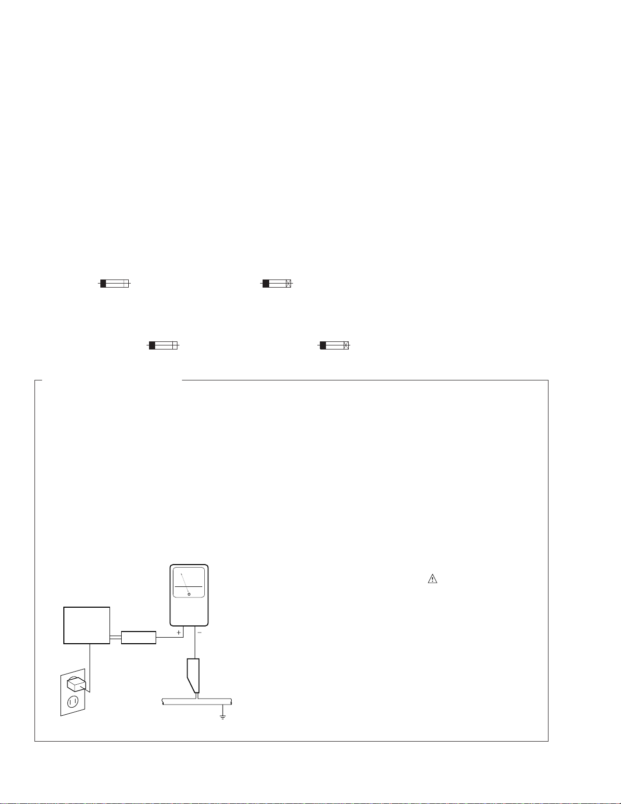
1. SAFETY PRECAUTIONS
The following check should be performed for the
continued protection of the customer and service
technician.
LEAKAGE CURRENT CHECK
Measure leakage current to a known earth ground
(water pipe, conduit, etc.) by connecting a leakage
current tester such as Simpson Model 229-2 or
equivalent between the earth ground and all exposed
metal parts of the appliance (input/output terminals,
screwheads, metal overlays, control shaft, etc.). Plug
the AC line cord of the appliance directly into a 120V
AC 60 Hz outlet and turn the AC power switch on. Any
current measured must not exceed 0.5 mA.
Reading should
not be above
0.5 mA
Earth ground
Device
under
test
Also test with plug
reversed
(Using AC adapter
plug as required)
Leakage
current
tester
Test all exposed
metal surfaces
AC Leakage Test
ANY MEASUREMENTS NOT WITHIN THE LIMITS
OUTLINED ABOVE ARE INDICATIVE OF A POTENTIAL SHOCK HAZARD AND MUST BE CORRECTED BEFORE RETURNING THE APPLIANCE
TO THE CUSTOMER.
2. PRODUCT SAFETY NOTICE
Many electrical and mechanical parts in the appliance have special safety related characteristics. These
are often not evident from visual inspection nor the
protection afforded by them necessarily can be obtained by using replacement components rated for
voltage, wattage , etc. Replacement parts which have
these special safety characteristics are identified in
this Service Manual.
Electrical components having such features are
identified by marking with a
on the parts list in this Service Manual.
The use of a substitute replacement component which
does not have the same safety characteristics as the
PIONEER recommended replacement one, shown in
the parts list in this Service Manual, may create shock,
fire, or other hazards.
Product Safety is continuously under review and
new instructions are issued from time to time. For
the latest information, always consult the current
PIONEER Service Manual. A subscription to, or additional copies of, PIONEER Service Manual may be
obtained at a nominal charge from PIONEER.
on the schematics and
2
Page 3
2. EXPLODED VIEWS AND PARTS LIST
NOTES : Parts marked by “ NSP ” are generally unavailable because they are not in our Master Spare Parts List.
The mark found on some component parts indicates the importance of the safety factor of the part.
Therefore, when replacing, be sure to use parts of identical designation.
Screw adjacent to mark on the product are used for disassembly.
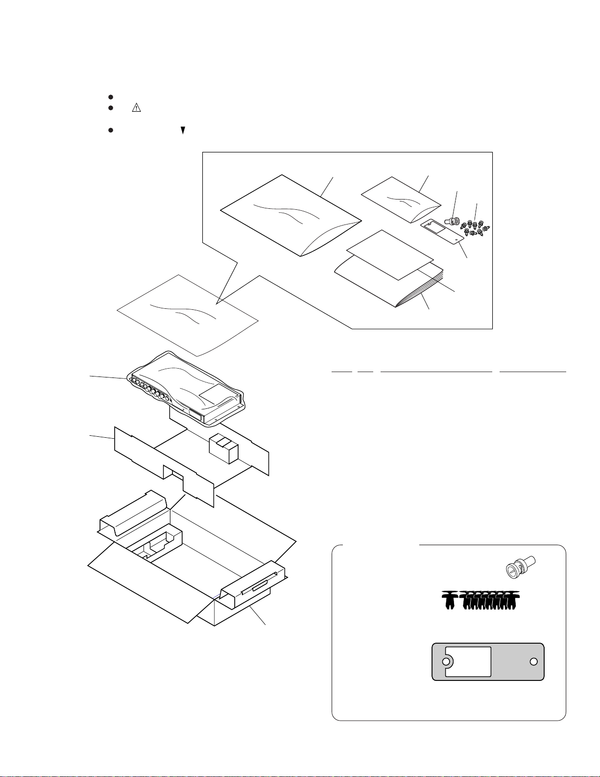
2.1 PACKING
PDA-5001
10
9
7
6
5
8
4
PACKING PARTS LIST
Mark No. Description Part No.
2
3
1 Packing Case AHD3042
2 Packing Sheet AHG1300
3 Card Board Protector AHA2257
4 Operating Instructions ARE1351
(English/French/German/Italian/
Dutch/Spanish)
5 Connector Cover ANG2356
6 Screw Rivet AEC1852
7 Pin/BNC Conversion Adaptor AKX1052
NSP 9 Vinyl Bag AHG–064
NSP 10 Literature Bag AHG-117
8 Caution Sheet ARM1177
Accessories
1 Pin/BNC conversion adaptor x 1
(AKX1052)
2 Screw rivets x 8
(AEC1852)
1
3 Connector cover x 1
(ANG2356)
÷ Operating Instructions
(ARE1351)
3
Page 4
PDA-5001
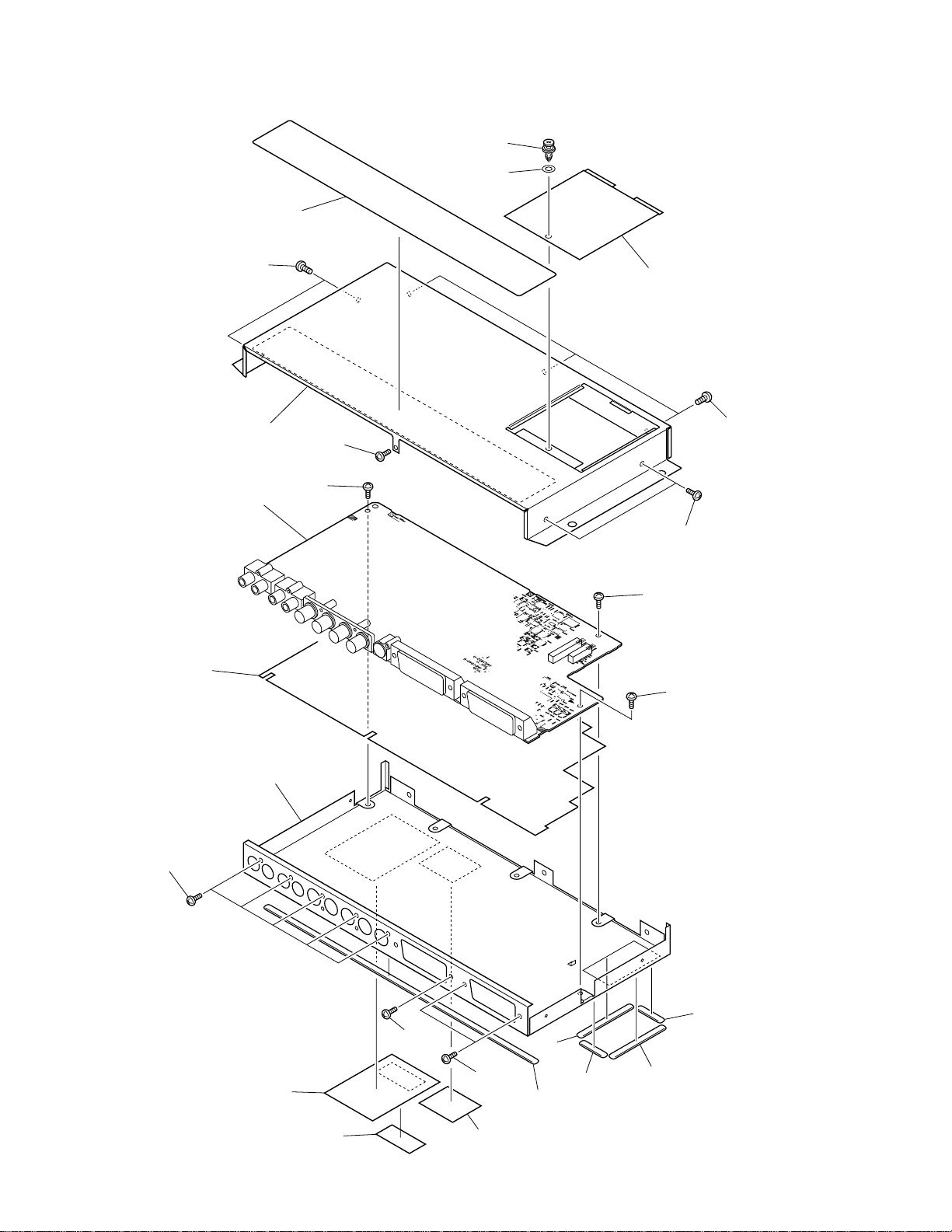
2.2 EXTERIOR
6
4
13
15
11
16
15
1
5
3
15
15
15
15
2
16
7
10
14
16
16
12
8
7
9
8
4
Page 5

EXTERIOR PARTS LIST
Mark No. Description Part No.
NSP 1 VIDEO Assy AWQ1052
NSP 2 Chassis ANA1612
3 Bonnet Cover ANG2357
4 Washer ABE1077
NSP 5 Insulating Sheet AEC1829
6 Screw Rivet AEC1852
7 Shield Gasket S ANK1636
8 Shield Gasket M ANK1637
9 Shield Gasket L ANK1638
10 Name Label AAL2318
11 Metal Bonnet ANE1585
NSP 12 UPC Code Label AAX2765
13 Label AAX2767
NSP 14 Label VRW1629
15 Screw BBZ30P050FZK
PDA-5001
16 Screw BBZ30P080FZK
17 Serial Seal AAX2609
5
Page 6
1
234
PDA-5001
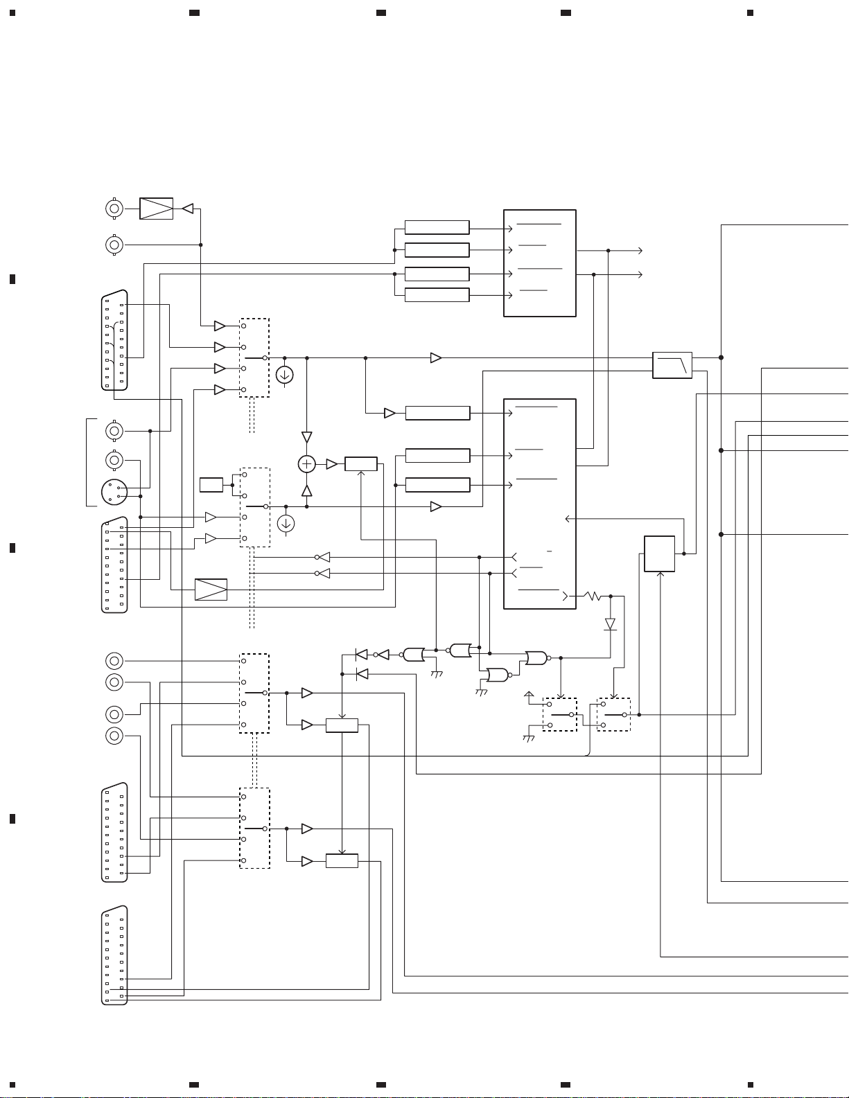
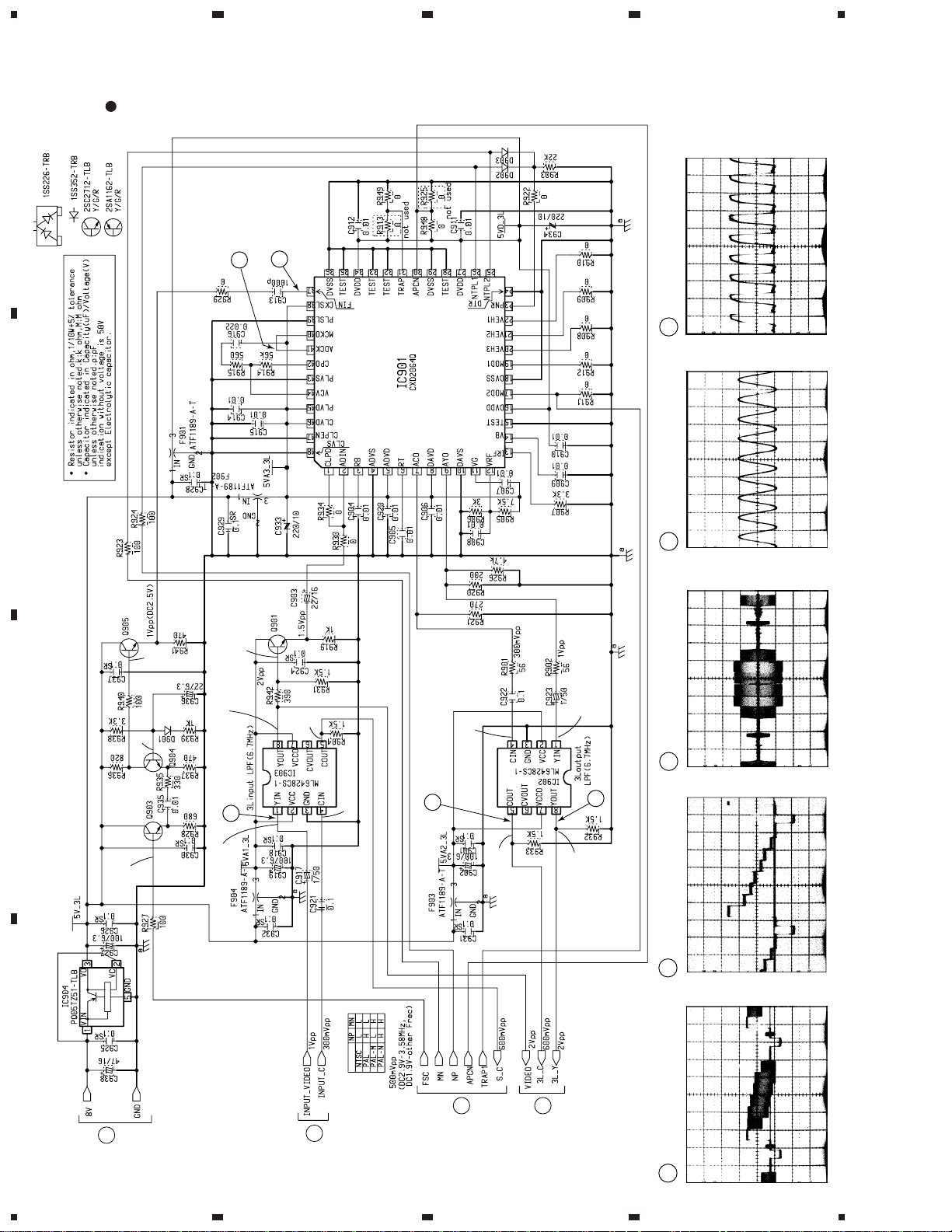
3. BLOCK DIAGRAM AND SCHEMATIC DIAGRAM
3.1 BLOCK DIAGRAM
A
B
INPUT1
BNC
VIDEO OUT
INPUT1
BNC
VIDEO IN
INPUT1
SCART
V/RGB IN
INPUT2
BNC/S
YC IN
INPUT2
SCART
V/YC IN
VIDEO OUT
IC103
MC14577CF
1
+6dB
C
C SELECTER
Bias
15
11
IC104
MC14577CF
+6dB
IC102
TC4052BF
1
5
2
4
IC102
TC4052BF
1
I/O BLOCK
COMP./Y
SELECTER
3
YC MIX
13
Switching voltage decode
for POWER SAVE etc.
Q120/Q121/Q122
S1/S2 DECORD
Q117
MUTE
Q137/Q138/Q140
Q135/Q136/Q139
Comparater
Comparater
Comparater
Comparater
Signal detect
Comparater
Comparater
CXA1875AM
4:3 Auto.1
Auto.1
4:3 Auto.2
Auto.2
COMP./Y
CXA1875AM
9
Signal det.
1
Squize
2
Letter box
Full RGB det.
7
Input1/2
6
Scart/other
RGB mode
IC105
S_C
IC106
SDA
SCK
IC903
ML6428CS-1
+6dB
10
Full RGB
10
Full
RGB
det.
5
Q115
INPUT2 &
SCART
RGB, BLK
On & Off Mute
IC101
TC4052BF
INPUT1
C
D
BNC
LR IN
INPUT2
BNC
LR IN
INPUT1
SCART
LR IN
INPUT2
SCART
LR IN
LR OUT
1
5
2
4
12
15
11
14
IC101
TC4052BF
(L)
3
AUDIO
SELECTER
(R)
13
MUTE
Q114
MUTE
INPUT1 &
SCART
5V
IC108
TC4053BF
CLP
BLK
RGB
S_C
SECAM,4.43NT_C
6
1234
Page 7
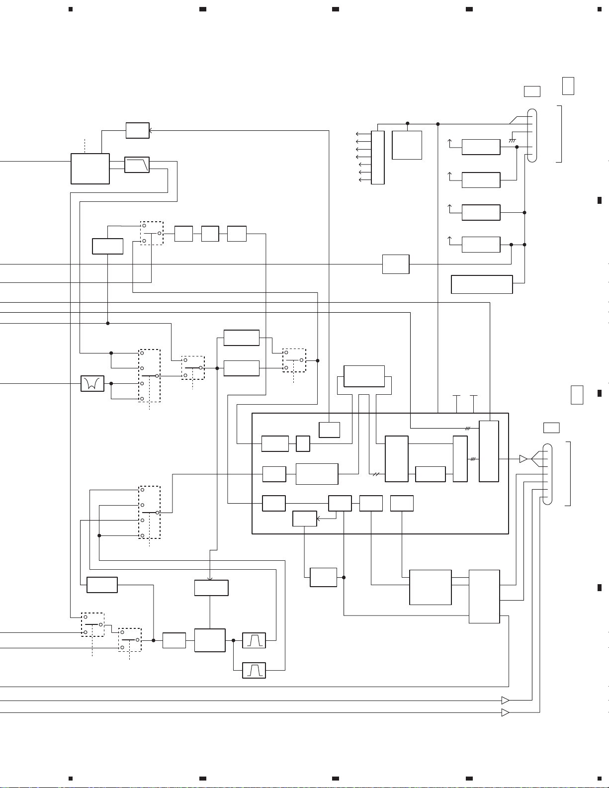
5
67
8
PDA-5001
3L Y/C BLOCK
MN, ANP
3L Y/C
IC901
CXD2064Q
SECAM
TRAP
fsc
ML6428CS-1
for RGB mode
6dB ATT
S_Y
NTSC
PAL
SECAM
4.43NT
Y/C SELECT BLOCK
NTSC
PAL
SECAM
4.43NT
6dB ATT
IC701
TC4053BF
NTSC,PAL_C
3
4
5
TRAP1
TC4053BF
1
2
AMP
IC902
+6dB
12
13
15
11
14
11
2
4
5
1
IC701
VS
IC704
TC4053BF
Y-SEL
IC702
TC4052BF
TRAP0,1
C-SEL
IC702
TC4052BF
TRAP0,1
15
Y
C
14
AMP LPF CLP
except RGB mode
SCART RGB
SinY/Y
SEL
IC701
TC4053BF
12
13 13
VS, BW
3
Y CLAMP
AMP
CNR
BLK
14
6dB ATT
for SECAM
250nS DL
except
SECAM
Y
45
C
42
SYNC
51
3.58BPF
4.43BPF
12
13
CLAMP
ACC
SYNC
SEP
IC704
TC4053BF
14
DL SW
DL
CROMA
DECORDER
H OUT
4
IC1202
TC74HC4538AF
FSC
OUT
H BLK.
GEN.
VS
BW
NP
MN
TRAP0
TRAP1
DL SW
AFC
10
CXA1875AM
Y PEAKING
AMP
V C/D
56
EXPANDER
IC703
Q1218
MUTE
CONT.
TRAST
V BLK
IC1203
NJM319W
E2PROM
VIDEO
DATA ROM
IC1208
24LC32A
CON-
SCP
OUT
1
Sand Casle
CLP PULSE
COLOR
CHROMA DECODE BLOCK
+5V
+5V
+12V
+9V
23,
24,
25
RGB DECODER
TB1227BN
GEN.
V BLK
INV.
H BLK
TC74VHCT541AFT
IC1207
PQ05TZ51
5V Reg.
IC904
PQ05TZ51
5V Reg.
IC1205
PQ20VZ1U
12V Reg.
IC1206
PQ20VZ1U
9V Reg.
ON&OFF MUTE
for SCART2 OUT
+5V3+9V
2241
RGB
SW
MATRIX
IC1201
C.P.
SYNC
BUFFER
12,
13,
14
VB1
CN1202
SCL
SDA
OPTION
8V
13.5V
VB2
CN1201
A
PDP-502MXE VIDEO ASSY CN304 A31
B
R
G
B
V.BLK
H.BLK
L
R
C
PDP-502MXE VIDEO ASSY CN503 A30
D
L
R
7
5
6
7
8
Page 8
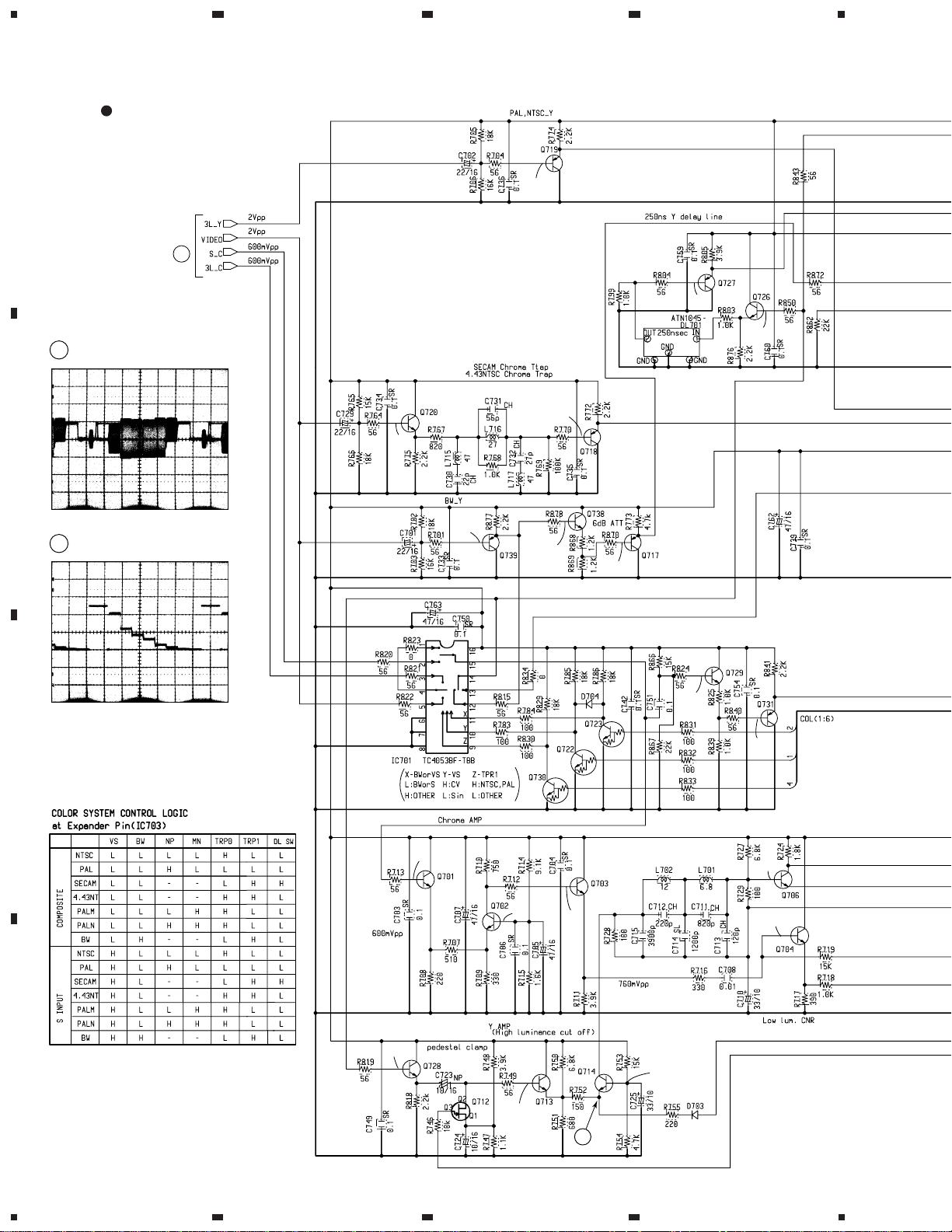
1
7
PDA-5001
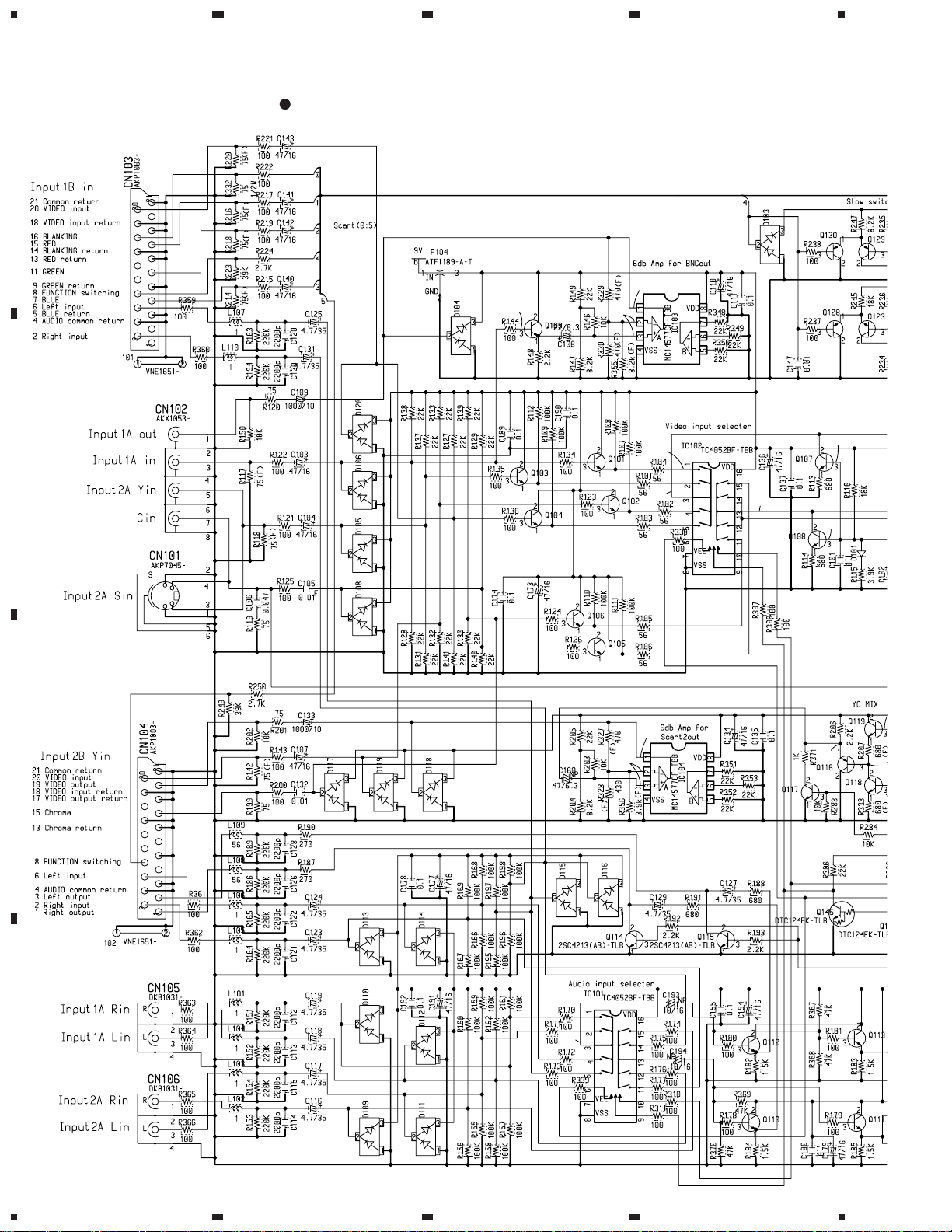
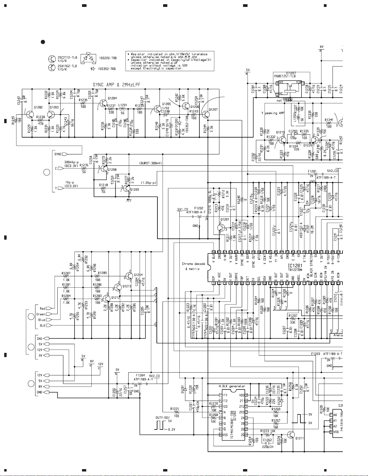
3.2 SCHEMATIC DIAGRAM
3.1.1 VIDEO ASSY (1/4)
I/O BLOCK
234
A
VIDEO ASSY (1/4) (AWQ1052)
I/O BLOCK
4.2
2.4
5.0
3.5
2.0
B
Q101–Q106 Base
Selected Function: 4.2
Other: 4.5
IC102 Input Pins
Selected Function: 3.5
Other: 9.0
3.3
3.3
2.0
5.2
C
4.5
2.4
4.5
4.3
3.
D
8
1234
Page 9
5
67
8
PDA-5001
Note: When ordering service parts, be sure to refer to "EXPLODED VIEWS AND PARTS LIST" or "PCB PARTS LIST".
To VIDEO ASSY (4/4)
F
CHROMA DECODE BLOCK
7.5
IC105
3.1
A
5.9
2.0
0
B
2.0
Q148 Emitter INPUT C
1
0.2 V/div., 10 µs/div.
6.3 –
4.3
3.7
2.6
∗
S Input
2.7V
2.5
1.2
Q147 Emitter
2
0.5 V/div., 10 µs/div.
INPUT VIDEO
IC106
– G
C
E
3.3
G
3.3
1
2
1.8
D
CHROMA DECODE BLOCK
C
D
To VIDEO ASSY (4/4)
To VIDEO ASSY (3/4)
B
To VIDEO ASSY (2/4)
A
3L Y/C BLOCK
Y/C SELECT BLOCK
9
5
6
7
8
Page 10
1
3
3
VIDEO ASSY (2/4) (AWQ1052)
3L Y/C BLOCK
To VIDEO ASSY (3/4)
Y/C SELECT BLOCK
To VIDEO ASSY (3/4)
Y/C SELECT BLOCK
To VIDEO ASSY (1/4)
I/O BLOCK
I
A
J
H
IC903 Pin1 Y IN
(Composite Video In)
0.5 V/div., 10 µs/div.
– G – G
4
IC902 Pin8 Y OUT
0.5 V/div., 10 µs/div.
– 1.9V
5
IC902 Pin5 C OUT
0.5 V/div., 10 µs/div.
– 2.4V
– G
6
IC901 Pin37 FIN (fsc)
0.5 V/div., 0.2 µs/div.
7
IC901 Pin41 ADCK (4fsc)
2 V/div., 50 ns/div.
3.8: NTSC
2.8: PAL
1.6
1.3
1.9
1.9
1.3
0.5
0
5.0
2.6
0.9
5.0
0
0
0
0
0
0
0
5.0
5.0
0
3.0
1.4
1.0
0
0
0
0
0
0
0
0
0 2.4
5.0
5.0
5.0
0
0
1.4
0.8V synctip clamped
0.9V synctip clamped
0.9V synctip
clamped 0.8V synctip
clamped
0.7V synctip clamped
3.3
4
5
6
7
Pin 1, 2: 0.7V synctip clamped
Pin 9: 0.1V synctip clamped
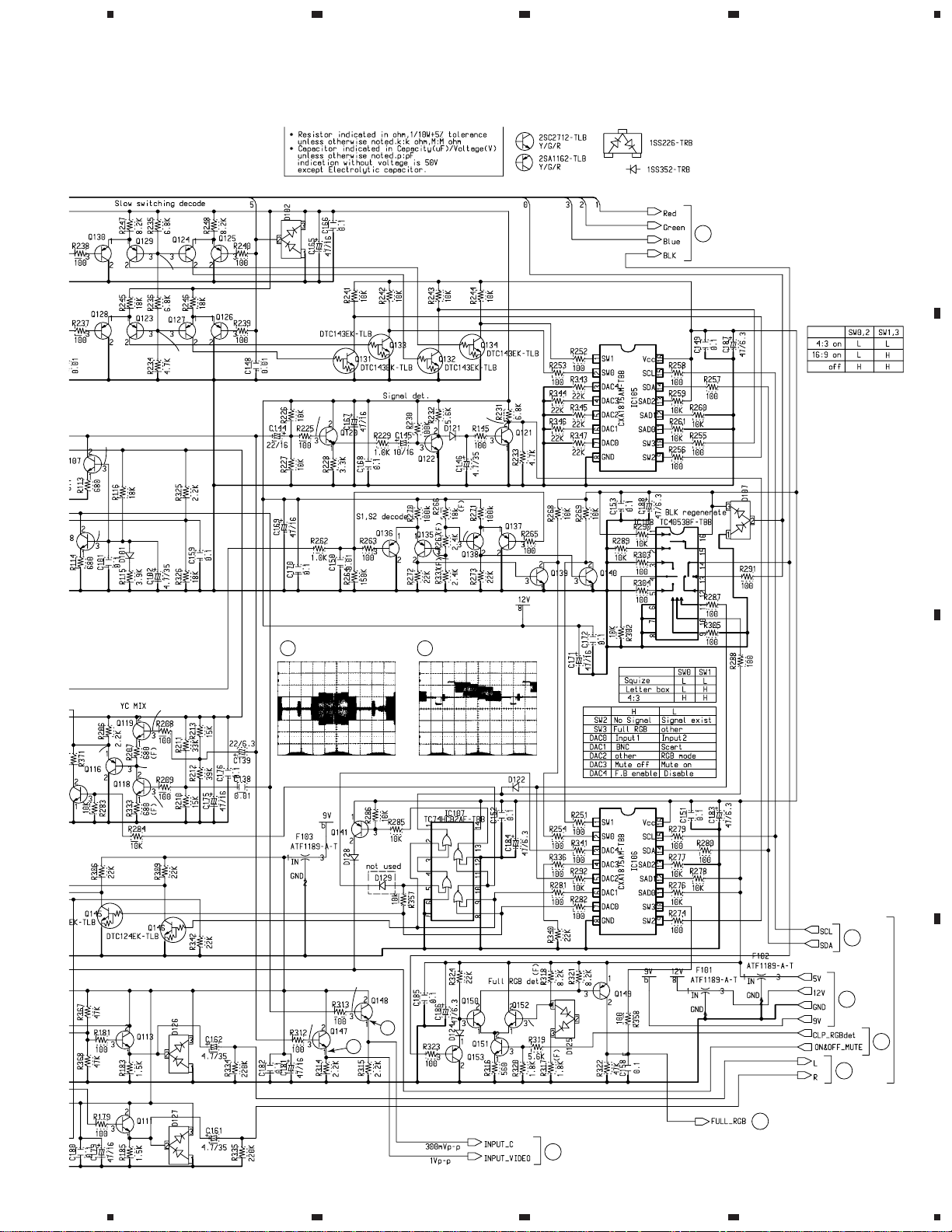
PDA-5001
3.1.2 VIDEO ASSY (2/4)
3L Y/C BLOCK
A
234
B
C
D
10
1234
Page 11
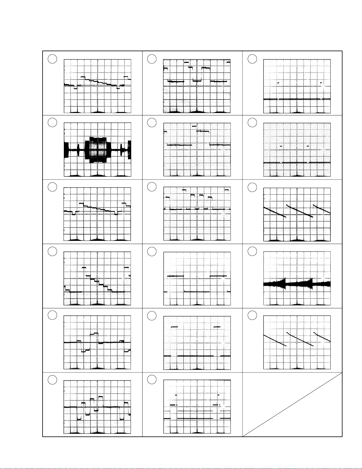
WAVEFORMS [ for VIDEO ASSY (4/4): CHROMA DECODE BLOCK ]
PDA-5001
10
IC1201
pin 45
Y1 IN
11
IC1201
pin 42
C IN
12
IC1201
pin 51
SYNC IN
0.5 V/div., 10 µs/div.
0.2 V/div., 10 µs/div.
0.5 V/div., 10 µs/div.
–
–
GND
3.5V
16
IC1201
pin 14
R OUT
17
IC1201
pin 13
G OUT
18
IC1201
pin 12
B OUT
0.5 V/div., 10 µs/div.
0.5 V/div., 10 µs/div.
0.5 V/div., 10 µs/div.
–
–
GND
GND
22
IC1201
pin 12
CLP
Pulse
23
IC1201
pin 7
V BLK
24
IC1201
pin 52
V RAMP
2 V/div., 10 µs/div.
2 V/div., 5 ms/div.
1 V/div., 5 ms/div.
–
–
GND
GND
13
IC1201
pin 37
Y OUT
14
IC1201
pin 35
R-Y OUT
15
IC1201
pin 36
B-Y OUT
0.2 V/div., 10 µs/div.
0.2 V/div., 10 µs/div.
0.2 V/div., 10 µs/div.
–
–
–
2V
1.8V
1.8V
19
IC1201
pin 4
H OUT
20
IC1201
pin 6
FBP
21
IC1201
pin 1
SCP
2 V/div., 10 µs/div.
2 V/div., 10 µs/div.
2 V/div., 10 µs/div.
–
–
–
GND
GND
GND
25
IC1201
pin 53
V OUT
26
IC1201
pin 54
V-NF
0.2 V/div., 5 ms/div.
1 V/div., 5 ms/div.
–
–
–
GND
GND
GND
–
GND
11
Page 12
1
PDA-5001
3.1.3 VIDEO ASSY (3/4)
Y/C SELECT BLOCK
A
To VIDEO ASSY (2/4)
3L Y/C BLOCK
234
5.8
H
VIDEO ASSY (3/4) (AWQ1052)
Y/C SELECTOR BLOCK
2.9
Q708 Emitter CNR output
8
1 V/div., 10 µs/div.
– 7.2V
5.8
6.5
6.4
B
Q714 Emitter Y+H. BLK add
9
0.5 V/div., 10 µs/div.
– 2.3V
5.8
6.4
2.9
7.0
3.2
C
1.9
1.8
6.4
D
2.6V
Pedestal
clamped
9.6
2.9
9
4.7
3.3
12
1234
Page 13
5
67
8
PDA-5001
6.4
2.9
3.5
I
J
3L Y/C BLOCK
To VIDEO ASSY (2/4)
A
B
4.7
3.8
8.0
8
7.4
7.4
4.2
3.5
3.5
M
L
K
To VIDEO ASSY (4/4)
B
To VIDEO ASSY (1/4)
I/O BLOCK
CHROMA DECODE BLOCK
C
D
13
5
6
7
8
Page 14
1
46
PDA-5001
3.1.4 VIDEO ASSY (4/4)
CHROMA DECODE BLOCK
A
234
4.2
3.5
M
B
Y/C SELECT BLOCK
3.7
5.5
3.5
2.8
2.4
3.6V
synctip
clamped
10.4
4.1
4.1
To VIDEO ASSY (3/4)
VIDEO ASSY (4/4) (AWQ1052)
CHROMA DECODE BLOCK
Q1212, Q1213, Q1214 Base: 3.7V
5.4
5.1
4.5
2.9
2.4
3.5
5.0
C
I/O BLOCK
To VIDEO ASSY (1/4)
Y/C SELECT BLOCK
D
To VIDEO ASSY (3/4)
0
9.0
5.0
4.4
4.5
9.0
2.6
7.6
4.6
0.2
0
0
0
F
G
K
14
1234
Page 15
5
0
67
8
PDA-5001
A
1.25
10.4
1.25
VIDEO ASSY CN304 A31
Q1215, Q1216, Q1217 Base: 2.3V pedestal
4.1
To PDP-502MXE
B
VIDEO ASSY CN503 A30
To PDP-502MXE
C
3.2
4.30
D
E
I/O BLOCK
To VIDEO ASSY (1/4)
0
0
0
0.2
4.6
4.6
4.6
2.4
C
23
22
L
Y/C SELECT BLOCK
To VIDEO ASSY (3/4)
Waveforms: 0 – ¡ are waveform Nos. on page 11.
0
: IC1201 pin45 Y1 IN
-
: IC1201 pin42 C IN
=
: IC1201 pin51 SYNC IN
~
: IC1201 pin37 Y OUT
!
: IC1201 pin35 R-Y OUT
@
: IC1201 pin36 B-Y OUT
#
: IC1201 pin14 R OUT
$
: IC1201 pin13 G OUT
%
: IC1201 pin12 B OUT
^
: IC1201 pin4 H OUT
&
: IC1201 pin6 FBP
*
: IC1201 pin1 SCP
(
: IC1201 pin12 CLP Pulse
)
: IC1201 pin7 V BLK
_
: IC1201 pin52 V RAMP
+
: IC1201 pin53 V OUT
¡
: IC1201 pin54 V-NF
D
15
5
6
7
8
Page 16
1
234
PDA-5001
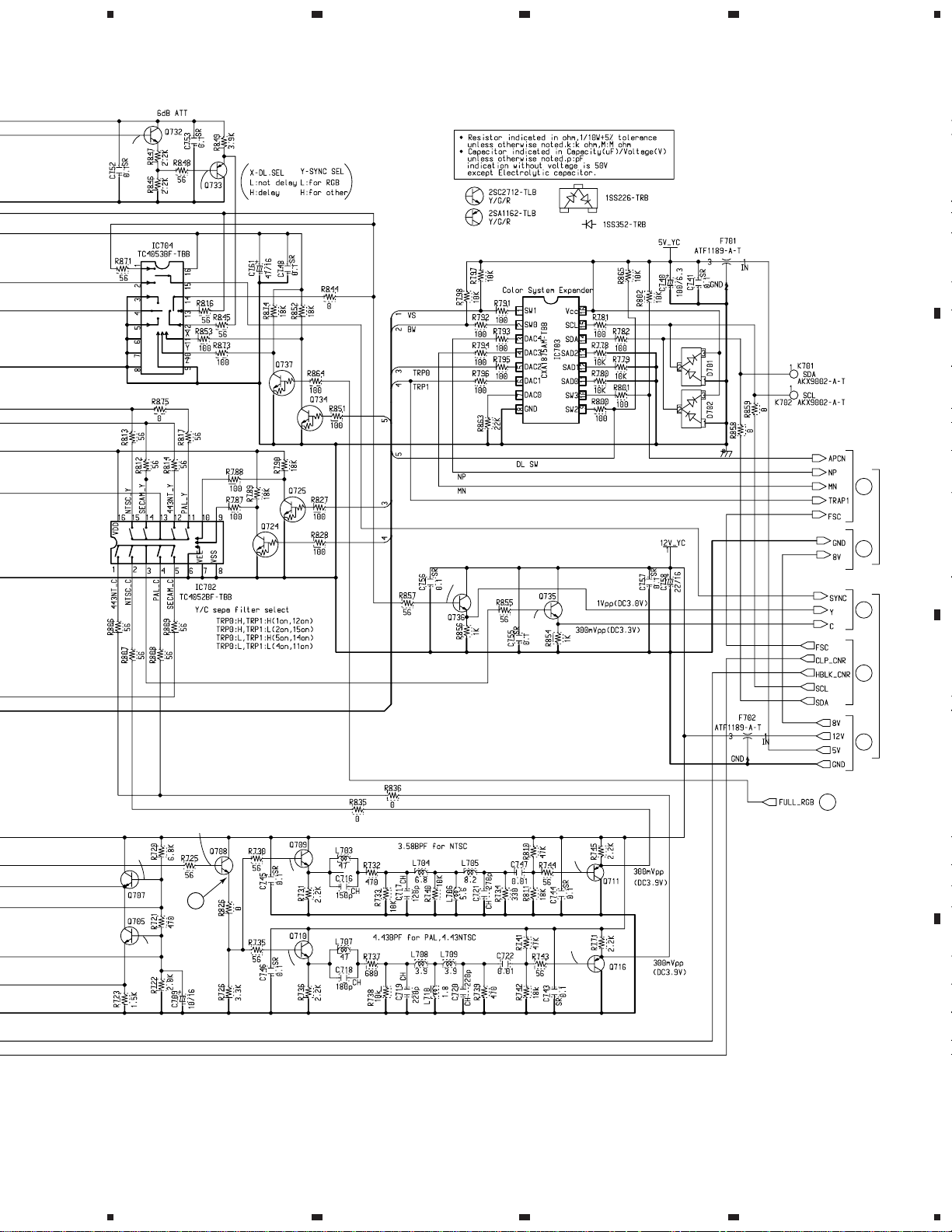
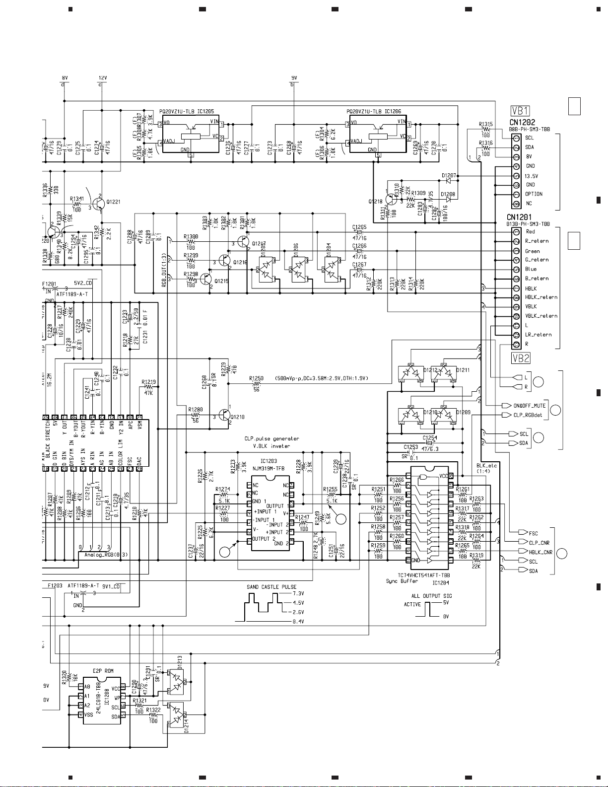
4. PCB CONNECTION DIAGRAM
VIDEO ASSY
A
B
(ANP1942–B)
C
D
CN503
CN304
A30
PDP-502MXE
VIDEO ASSY
SIDE A
A31
Q120Q1212–Q1214
Q121
Q122
Q141
NOTE FOR PCB DIAGRAMS:
1. Part numbers in PCB diagrams match those in the schematic
diagrams.
2. A comparison between the main parts of PCB and schematic
diagrams is shown below.
Symbol in PCB
Diagrams
BCE
BCE
Symbol in Schematic
Diagrams
BCE
BCEBCE
IC106
BCE
Q114
Q1215–Q1217
IC1208
Part Name
Transistor
Transistor
with resistor
Q115
Q1210
Symbol in PCB
Diagrams
DGS
IC108
Q1229
Symbol in Schematic
Diagrams
DGSDGS
Q1220
Q135–Q140
IC1201
Q1219
Part Name
Field effect
transistor
Resistor array
IC104
16
1234
Page 17
5
67
8
PDA-5001
A
B
IC104
Q104
Q102
Q116–Q119
IC1203
Symbol in PCB
Diagrams
3. The parts mounted on this PCB include all necessary parts
for several destination.
For further information for respective destinations, be sure
to check with the schematic diagram.
Q106
Q1211
Q1201–Q1209
Symbol in Schematic
Diagrams
IC1202
IC1204
IC102
Q108
Q149–Q153
Part Name
3-terminal
regulator
5
Q103 Q101
Q713
Q728
Q711
Q709
4. Viewpoint of PCB diagrams
Q727
Q708
P. C. Board Chip Part
6
Q109
IC704
IC703
C
IC103
Q148
Q717Q737
Q738
Q732
Q726
Q725
Q739
Q735
Q147
IC701
Q720
Q721
IC902
IC101
IC903
Q901
IC901IC702
D
CapacitorConnector
SIDE A
SIDE A
SIDE B
17
7
8
Page 18

PDA-5001
A
VIDEO ASSY
B
1
234
C
Q110–Q113
Q903–Q905
Q919
Q729
Q731
Q918
Q723
Q154
Q915
Q722
Q924
Q146
Q730
Q145
Q736
Q734
Q714
Q716Q701–Q703
Q704–Q707
Q107
Q710
D
18
1234
Page 19

5
67
8
PDA-5001
SIDE B
A
B
Q131–Q134
Q1218
(ANP1942–B)
C
Q123–Q130
D
19
5
6
7
8
Page 20

PDA-5001
5. PCB PARTS LIST
NOTES : ÷ Parts marked by “ NSP ” are generally unavailable because they are not in our Master Spare Parts List.
÷ The
÷ When ordering resistors, first convert resistance values into code form as shown in the following examples.
mark found on some component parts indicates the importance of the safety factor of the part.
Therefore, when replacing, be sure to use parts of identical designation.
Ex. 1 When there are 2 effective digits (any digit apart from 0), such as 560 ohm and 47k ohm (tolerance is shown by
J = 5%, and K = 10%).
560 Ω = 56 × 10
47k Ω = 47 × 10
1
= 561................................................... RD1/4PU 5 6 1 J
3
= 473 .................................................. RD1/4PU 4 7 3 J
0.5 Ω = R50 ...................................................................... RN2H Â 5 0 K
1 Ω = 1R0 ......................................................................... RS1P 1 Â 0 K
Ex. 2 When there are 3 effective digits (such as in high precision metal film resistors).
1
5.62k Ω = 562 × 10
= 5621 ........................................... RN1/4PC 5 6 2 1 F
Mark No. Description Part No.
VIDEO ASSY
SEMICONDUCTORS
IC1208 24LC64(I)SN
IC105, IC106, IC703 CXA1875AM
IC901 CXD2064Q
IC103, IC104 MC14577CF
IC902, IC903 ML6428CS-1
IC1203 NJM319M
IC1207, IC904 PQ05TZ51
IC1205, IC1206 PQ20VZ1U
IC1201 TB1227BN
IC101, IC102, IC702 TC4052BF
IC108, IC701, IC704 TC4053BF
IC107 TC74HC02AF
IC1202 TC74HC4538AF
IC1204 TC74VHCT541AFT
Q116, Q1208–Q1210, Q1215–Q1218 2SA1162
Q123–Q130, Q135–Q138, Q141 2SA1162
Q149, Q153, Q711, Q716–Q719 2SA1162
Q727, Q731, Q733, Q739 2SA1162
Q101–Q113, Q117–Q120 2SC2712
Q1201–Q1207, Q121, Q1211–Q1214 2SC2712
Q1219, Q122, Q1220, Q1221 2SC2712
Q139, Q140, Q147, Q148 2SC2712
Q150–Q152, Q701–Q710 2SC2712
Q713–Q715, Q720, Q726 2SC2712
Q728, Q729, Q732, Q735, Q736 2SC2712
Q738, Q901, Q903–Q905 2SC2712
Q114, Q115 2SC4213
Q712 2SK208
Q145, Q146, Q722–Q725, Q730 DTC124EK
Q734, Q737 DTC124EK
Q131–Q134 DTC143EK
D102–D120, D1204–D1206 1SS226
D1209–D1214, D125–D127 1SS226
D701, D702 1SS226
D101, D1201–D1203, D1207, D1208 1SS352
D121, D122, D124, D128 1SS352
D703, D704, D901–D903 1SS352
Mark No. Description Part No.
COILS AND FILTERS
F101–F104, F1201–F1204 ATF1189
F701, F702, F901–F904 ATF1189
DL701 ATN1045
L702 LCTA120J3225
L101–L107, L110 LCTA1R0J3225
L710 LCTA1R8J3225
L711, L716 LCTA270J3225
L708, L709 LCTA3R9J3225
L703, L707, L712, L715, L717 LCTA470J3225
L108, L109, L1201 LCTA560J3225
L706 LCTA5R6J3225
L701, L704 LCTA6R8J3225
L705 LCTA8R2J3225
CAPACITORS
C1263, C1264 (0.47 µF/16V) ACE1130
C1227 CCSQCH120J50
C1293, C713, C717 CCSQCH121J50
C716 CCSQCH151J50
C718 CCSQCH181J50
C730 CCSQCH220J50
C1262, C712, C719, C720 CCSQCH221J50
C728, C732 CCSQCH270J50
C1245, C1246, C721 CCSQCH271J50
C727 CCSQCH470J50
C1234, C1261 CCSQCH471J50
C731 CCSQCH560J50
C711 CCSQCH821J50
C1215 CCSQSL102J50
C714 CCSQSL122J50
C109, C133 CEAT102M10
C1228, C1243, C1249, C145, C709 CEV100M16
C724 CEV100M16
C1282 CEV101M16
C740, C902, C919, C927 CEV101M6R3
C1218, C1220, C1221, C1248, C917 CEV1R0M50
C923 CEV1R0M50
C1236, C1237, C1239, C1251, C1256 CEV220M16
C1292, C144, C701, C702, C726 CEV220M16
C729, C758, C903 CEV220M16
20
Page 21

PDA-5001
Mark No. Description Part No. Mark No. Description Part No.
C108, C139, C936 CEV220M6R3
C933, C934 CEV221M10
C1214, C1233 CEV2R2M50
C710, C725 CEV330M10
C103, C104, C107, C110, C1201 CEV470M16
C1206, C1209, C1225, C1229 CEV470M16
C1265–C1269, C1274, C1276, C1278 CEV470M16
C1280, C1284, C1288, C1294, C134 CEV470M16
C136, C140–C143, C154, C165 CEV470M16
C167, C169, C171, C173, C175 CEV470M16
C177, C179, C181, C191, C705 CEV470M16
C707, C761–C763, C938 CEV470M16
C1254, C1290, C183, C184 CEV470M6R3
C186–C188 CEV470M6R3
C102, C116–C119, C1210, C1223 CEV4R7M35
C123–C125, C127, C1283, C129 CEV4R7M35
C131, C146, C161, C162 CEV4R7M35
C193, C194, C723 CEVNP100M16
C160 CEVNP470M6R3
C1211–C1213, C1217, C1222, C158 CFHSP104J16
C105, C1219, C1224, C1231 CFHSQ103J16
C913 CKSQYB102K50
C1202–C1205, C1207, C1208, C1226 CKSQYB103K50
C1230, C132, C138, C147, C148 CKSQYB103K50
C150, C708, C722, C747 CKSQYB103K50
R327–R330 RS1/10S4700F
R1308 RS1/10S4701F
R1304 RS1/10S6201F
R207, R333 RS1/10S6800F
R117, R118, R142, R214, R216 RS1/10S75R0F
R218, R220 RS1/10S75R0F
R318, R355 RS1/10S8201F
R332 RS1/2S750J
Other Resistors RS1/10S J
OTHERS
CN103, CN104 CONNECTOR AKP1003
CN101 SOCKET AKP7045
102 CONNECTOR AKX1053
K701, K702 AKX9002
X1201 (16.2 MHz) ASS1152
CN1201 CONNECTOR B13B-PH-SM3
CN1202 CONNECTOR B8B-PH-SM3
JA105, JA106 JACK DKB1031
C904–C912, C914, C915, C920 CKSQYB103K50
C935 CKSQYB103K50
C1216, C1232, C1240, C1241, C751 CKSQYB104K25
C921, C922 CKSQYB104K25
C112–C115, C120–C122, C126 CKSQYB222K50
C128, C130 CKSQYB222K50
C916 CKSQYB223K50
C715 CKSQYB392K50
C106 CKSQYB473K50
C101, C111, C1235, C1238, C1242 CKSRYF104Z16
C1244, C1247, C1250, C1252, C1253 CKSRYF104Z16
C1255, C1257–C1260, C1270, C1273 CKSRYF104Z16
C1275, C1277, C1279, C1281, C1285 CKSRYF104Z16
C1289, C1291, C1295, C135, C137 CKSRYF104Z16
C149, C151–C153, C155, C159 CKSRYF104Z16
C166, C168, C170, C172, C174 CKSRYF104Z16
C176, C178, C180, C182, C185 CKSRYF104Z16
C189, C190, C192, C703, C704 CKSRYF104Z16
C706, C733–C739, C741–C746 CKSRYF104Z16
C748–C750, C752–C757 CKSRYF104Z16
C759, C760, C901, C918 CKSRYF104Z16
C924–C926, C928–C932, C937 CKSRYF104Z16
RESISTORS
R1305, R1306 RS1/10S1001F
R317 RS1/10S1801F
R266 RS1/10S1802F
R267, R331 RS1/10S2401F
R1307, R356 RS1/10S3901F
21
Page 22

PDA-5001
6. ADJUSTMENT
It is necessary to install VIDEO BOX PDA-5001 in Plasma Display PDP-502MXE to carry out the adjustment. Adjust PDA-5001 with
"VIDEO BOX" mode in Service Factory Mode of PDP-501MXE. Refer to Service Manual of PDP-502MXE/YVLDK (Order No.
ARP3037) for the details of Service Factory Mode.
Adjustment of PDA-5001 is necessary in order to supply decoded RGB signals at standard level to PDP-502MXE.
VIDEO BOX mode (Adjustment is independent of each signal)
Adjustment data is stored in EEPROM of VIDEO ASSY within Video Box.
Remote
Control
Key
1 CONTRAST Gain adjustment Adjustment required –––
2 BRIGHT Offset adjustment Adjustment required
3 COLOR Color Level adjustment Adjustment required –––
4 TINT Tint setting 64 ––– ––– 64 –––
5 RGB CONTRAST Gain adjustment ––– ––– ––– –––
6 Y DELAY Y-C Delay adjustment 2 0 3 0 –––
7 R GAIN Adjustment required
8 B GAIN Adjustment required
9 R-Y OFFSET Adjustment required –––
10 B-Y OFFSET Adjustment required –––
11 COLOR (Y MUTE) Color Level adjustment The same data as 3 –––
12 TINT (Y MUTE) Tint setting The same data as 4 –––
Adjustment
Parameter
Adjusting & Setting Item
NTSC PAL SECAM 4.43NTSC SCART RGB
Gain adjustment
Offset adjustment
Setting Value
Adjustment required
Adjusting Method
Waveform observing point: CN1201 VB2 RGB output (Pin1: R, Pin 3: G, Pin 5: B)
Procedure
Adjusting Item Input signal Adjusting Point Adjusting Method
Offset adjustment
1
VIDEO BOX in
Factory mode
R-Y OFFSET….…
"9" Key
B-Y OFFSET….…
"10" Key
B.B signal
or
STEP waveform
(No SETUP)
BRIGHT….…"2" Key
Adjust to match Blanking level and Signal 0% level at each RGB
output.
At this time, deviation among R,G, and B must be within 10mV.
Be careful of the deviation because G-output also varies in the ratio
shown in the following table when OFFSET data is changed.
BRIGHT 1 1 1
R-Y OFFSET – 0.5 1 0
B-Y OFFSET – 0.2 0 1
Match BLK period
In SCART RGB signal input, adjust to match Blanking level and Goutput 0% level using BRIGHT .
RGB
BLK period
22
Page 23

PDA-5001
Procedure
2
3
Adjusting Item Input signal Adjusting Point Adjusting Method
Gain adjustment
Color Level
adjustment
White 100%
signal
or
SETUP
waveform
(1 Vp-p)
(In SCART RGB
signal : 0.7 Vp-p)
75% Color bar
signal
VIDEO BOX in
Factory mode
CONTRAST ….…
"1" Key
R GAIN ….………
"7" Key
B GAIN ….………
"8" Key
RGB CONTRAST
….……… "5" Key
VIDEO BOX in
Factory mode
COLOR (Y MUTE)
….……… "11" Key
COLOR ….………
"3" Key
Adjust so that 0% to 100% level at each RGB output becomes
1.4Vp-p.
At this time, deviation among R,G,B must be within 30 mV.
1.4 Vp–p
In SCART RGB signal input, adjust them using RGB CONTRAST
instead of CONTRAST.
Adjust so that R-Y color-difference signal level at R-output becomes
1.4Vp-p ± 0.05V with remote control key.
1.4 Vp–p
Adjust it with key "3" when adjustment with LD pictures is required.
23
Page 24

PDA-5001
7. GENERAL INFORMATION
7.1 CONNECTION AND DISASSEMBLY
Connecting this unit to the display
This unit is to be used only when connected to the plasma
display, PDP-502MXE.
Before connecting this unit to the display, please be
sure to do the following:
÷ Undo any component or personal computer connections that
may have already been made to the plasma display.
÷ Make sure that the power of the plasma display is turned off, and
is unplugged from the wall outlet.
Precautions when connecting this unit to the display
When the covers on this unit and/or the display are opened to make
connections, be sure to avoid letting the screw rivets or their
respective parts fall into openings on the units.
CAUTION
This unit is designed only for connection to the plasma display,
PDP-502MXE. Do not alter or modify this unit in any way as it may
cause this unit to perform abnormally and/or may cause the plasma
display to malfunction.
3 Separate the two connector cables from the cover.
4 Pull the two connector cables through the slot on the connector
cover included with this unit.
Connector Cover
(Included with this unit)
To connect this unit to the plasma display PDP- 502MXE
1 Remove the cover plate on the back panel of the plasma display.
Unscrew using a philips
screwdriver (“+” head).
Note:
If for some reason the screws cannot
be unscrewed, use a tool or other
object with a tip flat enough to fit
between the screw and rivet and pry
the screw out as shown below.
Connector Cover
(PDP-502MXE side)
2 Remove the cover plate on the back panel of the plasma display.
The two cable connectors are attached to the inside of the cover
plate.
J123
8P Wire Assy
(ADX2554)
J122
13P Wire Assy
(ADX2553)
5 Secure the connector cover onto the display with 2 of the
included screw rivets.
Screw Rivet
24
Page 25

PDA-5001
6 Remove the cover on this unit.
When the cover is removed, the two connector terminals should
be clearly visible.
Screw Rivet
7 Align the holes on this unit with the corresponding holes on the
rear panel of the plasma display and secure this unit to the
plasma display using 4 of the included screw rivets.
2
3
1
4
8 Connect the connector cables to the respective terminals located
on the inside of this unit.
Make sure that connections are made correctly and securely.
J122
13P Wire Assy
(ADX2553)
J123
8P Wire Assy
(ADX2554)
CN1201 VB2
(PDA-5001 side)
CN1202 VB1
(PDA-5001 side)
9 Replace the cover of this unit.
Connection of this unit is complete.
PDP-502MXE
÷ When aligning this unit with the plasma display, be sure to bring
the two connector cables through this unit.
÷ Attach the screw rivets in the numbered order shown above. The
procedure for attaching the screw rivets is described in step 5.
÷ When connecting this unit to the plasma display, make sure that
the cable connectors are not pinched between the two units.
Disassembling the unit from the display
To remove this unit from the display, take the above steps in
reverse order.
25
Page 26

PDA-5001
8. PANEL FACILITIES AND SPECIFICATIONS
PANEL FACILITIES
123
R
SPEAKER
8 Ω – 16 Ω
+–
AUDIO OUTPUT
IN
OUT
COMBINATION
IN
CONTROL
OUT
RS-232C
4-098765
1 AUDIO INPUT (Pin jacks)
Use to obtain sound when INPUT2 (BNC/S) is selected.
Connect the audio output jack of components connected
to INPUT2 (BNC/S) to these jacks.
2 AUDIO INPUT (Pin jacks)
Use to obtain sound when INPUT1 (BNC) is selected.
Connect the audio output jack of components connected
to INPUT1 (BNC) to these jacks.
3 INPUT1 (BNC)
For connection of components that have a composite
video output jack.
Use the INPUT1 OUT jack to output the video signal to an
external monitor or other component.
Note: The video signal will not be output from the INPUT1
OUT jack when the main power of the plasma display is
off or in standby mode .
4 SPEAKER (R) terminal
For connection of an external right speaker.
Connect a speaker whose impedance is 8 -16 Ω.
5 AUDIO OUTPUT (Stereo mini jack)
Use to output the audio of the selected source component
connected to this unit.
6 COMBINATION IN/OUT
DO NOT MAKE ANY CONNECTIONS TO THESE
TERMINALS.
These terminals are used in the factory setup.
(INPUT 4)
AUDIO INPUT
R – L
(INPUT 3)
ANALOG
R G B
INPUT4
OUTPUT
ANALOG
(
R G B
(
7 CONTROL IN/OUT
For connection of PIONEER components that bear the Î
mark. Making CONTROL connection enables control of this
unit as a component in a system.
8 RS-232C
DO NOT MAKE ANY CONNECTIONS TO THIS
TERMINAL.
This terminal is used in the factory setup.
9 AUDIO INPUT (Stereo mini jack)
Use to obtain sound when INPUT4 is selected.
Connect the audio output jack of components connected
to INPUT4 to this jack.
0 AUDIO INPUT (Pin jacks)
Use to obtain sound when INPUT3 is selected. Connect
the audio output jack of components connected to INPUT3
to these jacks.
Note: The left audio channel (L) jack is not compatible
with monaural input sources.
- INPUT4
For connection of a personal computer (PC) or similar
component. Make sure that the connection made
corresponds to the format of the signal output from the
connected component.
Use the INPUT4 OUTPUT terminal to output the video
signal to an external monitor or other component.
Note: The video signal will not be output from the INPUT4
OUTPUT terminal when the main power of the plasma
display is off or in standby mode .
26
Page 27

PDA-5001
=~ !@
GBR
[ON SYNC] [H/V SYNC]
INPUT3
HD VD
75Ωj2.2kΩ
$%^&#
= INPUT2 (BNC/S)
For connection of components that have an S-video output
jack or Y/C separate video output jacks.
Note: Do not use both the S-VIDEO jack and the BNC
jacks in parallel. Doing so may cause this unit to
malfunction or become damaged.
~ INPUT2 (SCART)
For connection of a VCR or similar component compatible
with SCART connections.
! INPUT1 (SCART)
For connection of an A V component compatible with SCART
connections.
@ Video box connection cover
Remove when connecting this unit to the plasma display,
PDP-502MXE.
# INPUT3
For connection of components that have RGB or
component output jacks such as a personal computer , DVD
player, or external RGB decoder.
MAIN POWER
OFF ON
AC INLET
SPEAKER
8 Ω – 16 Ω
+–
L
$ Synchronizing signal impedance selector switch
Depending on the connections made at INPUT3, it may
be necessary to set this switch to match the output
impedance of the connected component’ s synchronization
signal.
When the output impedance of the component’s
synchronization signal is above 75 Ω, set this switch to
the 2.2 kΩ position.
% MAIN POWER switch
Use to switch the main power of the unit on and off.
^ AC INLET
Use to connect a power cord to an AC outlet.
& SPEAKER (L) terminal
For connection of an external left speaker. Connect a
speaker that has an impedance of 8 -16 Ω.
27
Page 28

PDA-5001
SPECIFICATIONS
General
External dimensions......... 338 (W) x 156 (H) x 30 (D) mm.
(including monitor)......... 1218 (W) x 737 (H) x 128 (D) mm
Weight...................................................................... 1.1 kg
(including plasma display monitor) ........................ 41.4 kg
Operating temperature range ............................ 0 to 40 °C
Input/output
Video
INPUT1 (BNC)
Input BNC jack
÷ Composite video signal
1 Vp-p/75 Ω/negative sync.
Output BNC jack
75 Ω /with buffer
INPUT 2 (BNC/S)
Input 1 S terminal (Mini DIN 4 pin)
2 BNC jack (x2)
÷ Y/C separate video signal
Y . . . 1 Vp-p/75 Ω/negative sync.
C . . .0.286 Vp-p/75 Ω (NTSC)
0.3 Vp-p/75 Ω (PAL)
Audio
Input INPUT 1
Pin jack (x2)
L/R ... 500mVrms/more than 10 kΩ
INPUT 2
Pin jack (x2)
L/R ... 500mVrms/more than 10 kΩ
INPUT1 (SCART)
Input SCART jack
÷ Composite video signal
1 Vp-p/75 Ω/negative sync.
÷ RGB signal
0.7 Vp-p/75 Ω
÷ Audio L/R. . .500 mVrms/more than 10 kΩ
INPUT2 (SCART)
Input SCART jack
÷ Composite video signal
1 Vp-p/75 Ω/negative sync.
÷ Y/C separate video signal
Y . . . 1 Vp-p/75 Ω/negative sync.
C . . .0.3 Vp-p/75 Ω (PAL)
0.286 Vp-p/75 Ω (NTSC)
÷ Audio L/R. . .500 mVrms/more than 10 kΩ
Output
÷ Composite video signal
1 Vp-p/75 Ω/negative sync.
÷ Audio L/R. . .500 mVrms/less than 1 kΩ
Accessories
Pin/BNC conversion adaptor ............................................ 1
Screw rivets ..................................................................... 8
Connector cover............................................................... 1
Operating Instructions...................................................... 1
28
÷ Due to improvements, specifications and design are subject to
change without notice.
Page 29

VIDEO BOX
PDA-5001
THIS MANUAL IS APPLICABLE TO THE FOLLOWING MODEL(S) AND TYPE(S).
ORDER NO.
ARP3038
Type
ZYVLPK DC power supplied from other system component
This unit is designed only for connection to the plasma display, PDP-502MXE. Do not alter or
modify this unit in any way as it may cause this unit to perform abnormally and/or may cause the
plasma display to malfunction.
Model
PDA-5001
Power Requirement
Remarks
This service manual should be used together with the following manual(s):
Model No.
PDP-502MXE
ARP3037
RemarksOrder No.
CONTENTS
1. SAFETY INFORMATION....................................2
2. EXPLODED VIEWS AND PARTS LIST .............3
3. BLOCK DIAGRAM AND SCHEMATIC DIAGRAM
.........................................................6
4. PCB CONNECTION DIAGRAM .......................16
5. PCB PARTS LIST.............................................20
6. ADJUSTMENT.................................................. 22
7. GENERAL INFORMATION .............................. 24
7.1 CONNECTION AND DISASSEMBLY ........ 24
8. PANEL FACILITIES AND SPECIFICATIONS
.......................................................26
PIONEER CORPORATION 4-1, Meguro 1-Chome, Meguro-ku, Tokyo 153-8654, Japan
PIONEER ELECTRONICS SERVICE, INC. P.O. Box 1760, Long Beach, CA 90801-1760, U.S.A.
PIONEER ELECTRONIC (EUROPE) N.V. Haven 1087, Keetberglaan 1, 9120 Melsele, Belgium
PIONEER ELECTRONICS ASIACENTRE PTE. LTD. 253 Alexandra Road, #04-01, Singapore 159936
PIONEER CORPORATION 1999
O–ZZR OCT. 1999 Printed in Japan
Page 30

PDA-5001
1. SAFETY INFORMATION
This service manual is intended for qualified service technicians; it is not meant for the casual
do-it-yourselfer. Qualified technicians have the necessary test equipment and tools, and have been
trained to properly and safely repair complex products such as those covered by this manual.
Improperly performed repairs can adversely affect the safety and reliability of the product and may
void the warranty. If you are not qualified to perform the repair of this product properly and safely, you
should not risk trying to do so and refer the repair to a qualified service technician.
WARNING
This product contains lead in solder and certain electrical parts contain chemicals which are known to the state of California to
cause cancer, birth defects or other reproductive harm.
Health & Safety Code Section 25249.6 – Proposition 65
NOTICE
(FOR CANADIAN MODEL ONLY)
Fuse symbols (fast operating fuse) and/or (slow operating fuse) on PCB indicate that replacement parts
must be of identical designation.
REMARQUE
(POUR MODÈLE CANADIEN SEULEMENT)
Les symboles de fusible (fusible de type rapide) et/ou (fusible de type lent) sur CCI indiquent que les
pièces de remplacement doivent avoir la même désignation.
(FOR USA MODEL ONLY)
1. SAFETY PRECAUTIONS
The following check should be performed for the
continued protection of the customer and service
technician.
LEAKAGE CURRENT CHECK
Measure leakage current to a known earth ground
(water pipe, conduit, etc.) by connecting a leakage
current tester such as Simpson Model 229-2 or
equivalent between the earth ground and all exposed
metal parts of the appliance (input/output terminals,
screwheads, metal overlays, control shaft, etc.). Plug
the AC line cord of the appliance directly into a 120V
AC 60 Hz outlet and turn the AC power switch on. Any
current measured must not exceed 0.5 mA.
Reading should
not be above
0.5 mA
Earth ground
Device
under
test
Also test with plug
reversed
(Using AC adapter
plug as required)
Leakage
current
tester
Test all exposed
metal surfaces
AC Leakage Test
ANY MEASUREMENTS NOT WITHIN THE LIMITS
OUTLINED ABOVE ARE INDICATIVE OF A POTENTIAL SHOCK HAZARD AND MUST BE CORRECTED BEFORE RETURNING THE APPLIANCE
TO THE CUSTOMER.
2. PRODUCT SAFETY NOTICE
Many electrical and mechanical parts in the appliance have special safety related characteristics. These
are often not evident from visual inspection nor the
protection afforded by them necessarily can be obtained by using replacement components rated for
voltage, wattage , etc. Replacement parts which have
these special safety characteristics are identified in
this Service Manual.
Electrical components having such features are
identified by marking with a
on the parts list in this Service Manual.
The use of a substitute replacement component which
does not have the same safety characteristics as the
PIONEER recommended replacement one, shown in
the parts list in this Service Manual, may create shock,
fire, or other hazards.
Product Safety is continuously under review and
new instructions are issued from time to time. For
the latest information, always consult the current
PIONEER Service Manual. A subscription to, or additional copies of, PIONEER Service Manual may be
obtained at a nominal charge from PIONEER.
on the schematics and
2
Page 31

2. EXPLODED VIEWS AND PARTS LIST
NOTES : Parts marked by “ NSP ” are generally unavailable because they are not in our Master Spare Parts List.
The mark found on some component parts indicates the importance of the safety factor of the part.
Therefore, when replacing, be sure to use parts of identical designation.
Screw adjacent to mark on the product are used for disassembly.
2.1 PACKING
10
6
9
7
5
4
PDA-5001
PACKING PARTS LIST
2
8
3
Mark No. Description Part No.
1 Packing Case AHD3042
2 Packing Sheet AHG1300
3 Card Board Protector AHA2257
4 Operating Instructions ARE1351
(English/French/German/Italian/
Dutch/Spanish)
5 Connector Cover ANG2356
6 Screw Rivet AEC1852
7 Pin/BNC Conversion Adaptor AKX1052
8 Caution Sheet ARM1177
NSP 9 Vinyl Bag AHG–064
NSP 10 Literature Bag AHG-117
Accessories
1 Pin/BNC conversion adaptor x 1
(AKX1052)
2 Screw rivets x 8
(AEC1852)
1
3 Connector cover x 1
(ANG2356)
÷ Operating Instructions
(ARE1351)
3
Page 32

PDA-5001
2.2 EXTERIOR
17
6
4
13
15
3
16
11
1
5
9
16
15
15
15
15
2
15
7
10
14
16
16
12
8
7
9
8
4
Page 33

EXTERIOR PARTS LIST
Mark No. Description Part No.
NSP 1 VIDEO Assy AWQ1052
NSP 2 Chassis ANA1612
3 Bonnet Cover ANG2357
4 Washer ABE1077
NSP 5 Insulating Sheet AEC1829
6 Screw Rivet AEC1852
7 Shield Gasket S ANK1636
8 Shield Gasket M ANK1637
9 Shield Gasket L ANK1638
10 Name Label AAL2318
11 Metal Bonnet ANE1585
NSP 12 UPC Code Label AAX2765
13 Label AAX2767
NSP 14 Label VRW1629
15 Screw BBZ30P050FZK
PDA-5001
16 Screw BBZ30P080FZK
17 Serial Seal AAX2609
5
Page 34

1
234
PDA-5001
3. BLOCK DIAGRAM AND SCHEMATIC DIAGRAM
3.1 BLOCK DIAGRAM
A
B
C
INPUT1
BNC
VIDEO OUT
INPUT1
BNC
VIDEO IN
INPUT1
SCART
V/RGB IN
INPUT2
BNC/S
YC IN
INPUT2
SCART
V/YC IN
VIDEO OUT
INPUT1
BNC
LR IN
INPUT2
BNC
LR IN
INPUT1
SCART
LR IN
IC103
MC14577CF
1
+6dB
C
C SELECTER
Bias
15
11
IC104
MC14577CF
1
+6dB
12
14
15
11
IC102
TC4052BF
1
5
2
4
IC102
TC4052BF
IC101
TC4052BF
1
5
2
4
SELECTER
IC101
TC4052BF
I/O BLOCK
COMP./Y
SELECTER
3
YC MIX
13
(L)
3
AUDIO
(R)
13
Q114
MUTE
MUTE
Switching voltage decode
for POWER SAVE etc.
Q120/Q121/Q122
S1/S2 DECORD
Q117
MUTE
INPUT2 &
SCART
Q115
Comparater
Comparater
Comparater
Comparater
Signal detect
Q137/Q138/Q140
Comparater
Q135/Q136/Q139
Comparater
RGB, BLK
On & Off Mute
CXA1875AM
4:3 Auto.1
Auto.1
4:3 Auto.2
COMP./Y
CXA1875AM
9
Signal det.
1
Squize
2
Letter box
Full RGB det.
7
Input1/2
6
RGB mode
5V
IC105
Auto.2
S_C
IC106
Scart/other
10
5
INPUT1 &
SCART
IC108
TC4053BF
SDA
SCL
IC903
ML6428CS-1
+6dB
Full
RGB
det.
BLK
RGB
CLP
Full RGB
S_C
SECAM,4.43NT_C
D
INPUT2
SCART
LR IN
LR OUT
6
1234
Page 35

5
67
8
PDA-5001
3L Y/C BLOCK
MN, NP
3L Y/C
IC901
CXD2064Q
SECAM
TRAP
fsc
ML6428CS-1
for RGB mode
6dB ATT
S_Y
NTSC
PAL
SECAM
4.43NT
Y/C SELECT BLOCK
NTSC
PAL
SECAM
4.43NT
6dB ATT
IC701
TC4053BF
NTSC,PAL_C
3
4
5
TRAP1
TC4053BF
1
2
AMP
IC902
+6dB
15
11
14
12
2
4
5
1
IC701
VS
IC704
TC4053BF
2
1
Y-SEL
IC702
TC4052BF
TRAP0,1
C-SEL
IC702
TC4052BF
TRAP0,1
15
Y
C
15
AMP LPF CLP
except RGB mode
SCART RGB
SinY/Y
SEL
IC701
TC4053BF
12
13 13
VS, BW
3
Y CLAMP
AMP
CNR
BLK
14
6dB ATT
for SECAM
250nS DL
except
SECAM
Y
45
C
42
SYNC
51
3.58BPF
4.43BPF
12
13
CLAMP
ACC
SYNC
SEP
IC704
TC4053BF
14
DL SW
DL
CROMA
DECORDER
H OUT
4
IC1202
TC74HC4538AF
FSC
OUT
H BLK.
GEN.
VS
BW
NP
MN
TRAP0
TRAP1
DL SW
AFC
6
CXA1875AM
Y PEAKING
AMP
V C/D
56
EXPANDER
IC703
Q1218
MUTE
CONT.
TRAST
V BLK
IC1203
NJM319M
E2PROM
VIDEO
DATA ROM
IC1208
24LC32A
23,
24,
25
CON-
SCP
OUT
1
Sand Casle
CLP PULSE
COLOR
CHROMA DECODE BLOCK
+5V
+5V
+12V
+9V
RGB DECODER
TB1227BN
GEN.
V BLK
INV.
H BLK
TC74VHCT541AFT
+5V
8,
38,
41
IC1201
C.P.
IC1207
PQ05TZ51
5V Reg.
IC904
PQ05TZ51
5V Reg.
IC1205
PQ20VZ1U
12V Reg.
IC1206
PQ20VZ1U
9V Reg.
+9V
3,
17
22
RGB
SW
MATRIX
SYNC
BUFFER
IC1204
12,
13,
14
VB2
CN1202
SCL
SDA
OPTION
8V
13.5V
VB1
CN1201
A
PDP-502MXE VIDEO ASSY CN304 A31
B
R
G
B
V.BLK
H.BLK
L
R
C
PDP-502MXE VIDEO ASSY CN503 A30
D
7
5
6
7
8
Page 36

1
7
PDA-5001
3.2 SCHEMATIC DIAGRAM
3.1.1 VIDEO ASSY (1/4)
I/O BLOCK
234
A
VIDEO ASSY (1/4) (AWQ1052)
I/O BLOCK
4.2
2.4
5.0
3.5
2.0
B
Q101–Q106 Base
Selected Function: 4.2
Other: 4.5
IC102 Input Pins
Selected Function: 3.5
Other: 9.0
3.3
3.3
2.0
5.2
C
4.5
2.4
4.5
4.3
3.
D
8
1234
Page 37

5
67
8
PDA-5001
Note: When ordering service parts, be sure to refer to "EXPLODED VIEWS AND PARTS LIST" or "PCB PARTS LIST".
To VIDEO ASSY (4/4)
F
CHROMA DECODE BLOCK
7.5
IC105
3.1
A
5.9
2.0
0
B
2.0
Input Signal: PAL EBU Color bar signal
Q148 Emitter INPUT C
1
0.2 V/div., 10 µs/div.
6.3
4.3
3.7
2.6
∗
S Input
–
2.7V
2.5
1.2
Q147 Emitter
2
0.5 V/div., 10 µs/div.
INPUT VIDEO
– G
IC106
C
E
3.3
G
3.3
1
2
1.8
D
CHROMA DECODE BLOCK
C
D
To VIDEO ASSY (4/4)
To VIDEO ASSY (3/4)
B
To VIDEO ASSY (2/4)
A
3L Y/C BLOCK
Y/C SELECT BLOCK
9
5
6
7
8
Page 38

1
3
3
VIDEO ASSY (2/4) (AWQ1052)
3L Y/C BLOCK
Waveforms
To VIDEO ASSY (3/4)
Y/C SELECT BLOCK
To VIDEO ASSY (3/4)
Y/C SELECT BLOCK
To VIDEO ASSY (1/4)
I/O BLOCK
I
A
J
H
IC903 Pin1 Y IN
(Composite Video In)
0.5 V/div., 10 µs/div.
Input Signal: PAL EBU Color bar signal
– G
– G
4
IC902 Pin8 Y OUT
0.5 V/div., 10 µs/div.
– 1.9V
5
IC902 Pin5 C OUT
0.5 V/div., 10 µs/div.
– 2.4V
– G
6
IC901 Pin37 FIN (fsc)
0.5 V/div., 0.2 µs/div.
7
IC901 Pin41 ADCK (4fsc)
2 V/div., 50 ns/div.
3.8: NTSC
2.8: PAL
1.6
1.3
1.9
1.9
1.3
0.505.0
2.6
0.9
5.0
5.0
0
0
0
0
0
0
5.0
5.0
0
3.0
1.4
1.0
0
5.0
0
0
0
0
0
0
0 2.4
5.0
5.0
2.0
2.0
5.0
0
0
1.4
0.8V synctip clamped
0.9V synctip clamped
0.9V synctip
clamped 0.8V synctip
clamped
0.7V synctip clamped
3.3
4
5
6
7
Pin 1, 2: 0.7V synctip clamped
Pin 9: 0.1V synctip clamped
PDA-5001
3.1.2 VIDEO ASSY (2/4)
3L Y/C BLOCK
A
234
B
C
D
10
1234
Page 39

PDA-5001
WAVEFORMS [ for VIDEO ASSY (4/4): CHROMA DECODE BLOCK ]
10
IC1201
pin 45
Y1 IN
11
IC1201
pin 42
C IN
12
IC1201
pin 51
SYNC IN
0.5 V/div., 10 µs/div.
0.2 V/div., 10 µs/div.
0.5 V/div., 10 µs/div.
–
–
GND
3.5V
16
IC1201
pin 14
R OUT
17
IC1201
pin 13
G OUT
18
IC1201
pin 12
B OUT
0.5 V/div., 10 µs/div.
0.5 V/div., 10 µs/div.
0.5 V/div., 10 µs/div.
–
–
GND
GND
∗: Input Signal: PAL EBU Color bar signal
22
IC1203
pin 12
CLP
Pulse
23
IC1203
pin 7
V BLK
24
IC1201
pin 52
V RAMP
2 V/div., 10 µs/div.
2 V/div., 5 ms/div.
1 V/div., 5 ms/div.
–
–
GND
GND
13
IC1201
pin 37
Y OUT
14
IC1201
pin 35
R-Y OUT
15
IC1201
pin 36
B-Y OUT
0.2 V/div., 10 µs/div.
0.2 V/div., 10 µs/div.
0.2 V/div., 10 µs/div.
–
–
–
2V
1.8V
1.8V
19
IC1201
pin 4
H OUT
20
IC1201
pin 6
FBP
21
IC1201
pin 1
SCP
2 V/div., 10 µs/div.
2 V/div., 10 µs/div.
2 V/div., 10 µs/div.
–
–
–
GND
GND
GND
25
IC1201
pin 53
V OUT
26
IC1201
pin 54
V-NF
0.2 V/div., 5 ms/div.
1 V/div., 5 ms/div.
–
–
–
GND
GND
GND
–
GND
11
Page 40

1
PDA-5001
3.1.3 VIDEO ASSY (3/4)
Y/C SELECT BLOCK
234
A
To VIDEO ASSY (2/4)
3L Y/C BLOCK
Waveforms
Input Signal: PAL EBU Color bar signal
B
Q708 Emitter CNR output
8
1 V/div., 10 µs/div.
5.8
H
VIDEO ASSY (3/4) (AWQ1052)
– 7.2V
Y/C SELECTOR BLOCK
5.8
6.5
5.8
6.4
2.9
2.9
6.4
Q714 Emitter Y+H. BLK add
9
0.5 V/div., 10 µs/div.
C
– 2.3V
6.4
1.9
1.8
9.6
D
2.6V
Pedestal
clamped
9
7.0
3.2
4.7
3.3
2.9
12
1234
Page 41
6.4
2.9
5
67
8
PDA-5001
A
4.7
B
3L Y/C BLOCK
To VIDEO ASSY (2/4)
3.5
4.2
I
J
M
L
K
CHROMA DECODE BLOCK
To VIDEO ASSY (4/4)
C
B
8.0
3.5
7.4
To VIDEO ASSY (1/4)
I/O BLOCK
8
3.8
3.5
7.4
D
13
5
6
7
8
Page 42

1
46
PDA-5001
3.1.4 VIDEO ASSY (4/4)
CHROMA DECODE BLOCK
A
234
4.2
3.5
M
B
Y/C SELECT BLOCK
3.7
5.5
3.5
2.8
2.4
3.6V
synctip
clamped
10.4
4.1
4.1
To VIDEO ASSY (3/4)
VIDEO ASSY (4/4) (AWQ1052)
CHROMA DECODE BLOCK
5.4
5.1
4.5
2.9
2.4
3.5
5.0
2.8
3.7
C
To VIDEO ASSY (1/4)
D
To VIDEO ASSY (3/4)
F
G
I/O BLOCK
K
Y/C SELECT BLOCK
3.7
0
0
0
0
9.0
3.7
2.6
5.0
4.4
4.5
9.0
7.6
4.6
0.2
14
1234
Page 43

5
2
8
0
67
8
PDA-5001
A
1.25
10.4
1.25
VIDEO ASSY CN304 A31
To PDP-502MXE
4.1
2.3
2.3
2.3
B
VIDEO ASSY CN503 A30
To PDP-502MXE
C
.
3.2
4.30
D
E
I/O BLOCK
To VIDEO ASSY (1/4)
0
0
0
0.2
4.6
4.6
4.6
2.4
C
23
22
L
Y/C SELECT BLOCK
To VIDEO ASSY (3/4)
Waveforms: 0 – ¡ are waveform Nos. on page 11.
0
: IC1201 pin45 Y1 IN
-
: IC1201 pin42 C IN
=
: IC1201 pin51 SYNC IN
~
: IC1201 pin37 Y OUT
!
: IC1201 pin35 R-Y OUT
@
: IC1201 pin36 B-Y OUT
#
: IC1201 pin14 R OUT
$
: IC1201 pin13 G OUT
%
: IC1201 pin12 B OUT
^
: IC1201 pin4 H OUT
&
: IC1201 pin6 FBP
*
: IC1201 pin1 SCP
(
: IC1203 pin12 CLP Pulse
)
: IC1203 pin7 V BLK
_
: IC1201 pin52 V RAMP
+
: IC1201 pin53 V OUT
¡
: IC1201 pin54 V-NF
D
15
5
6
7
8
Page 44

1
234
PDA-5001
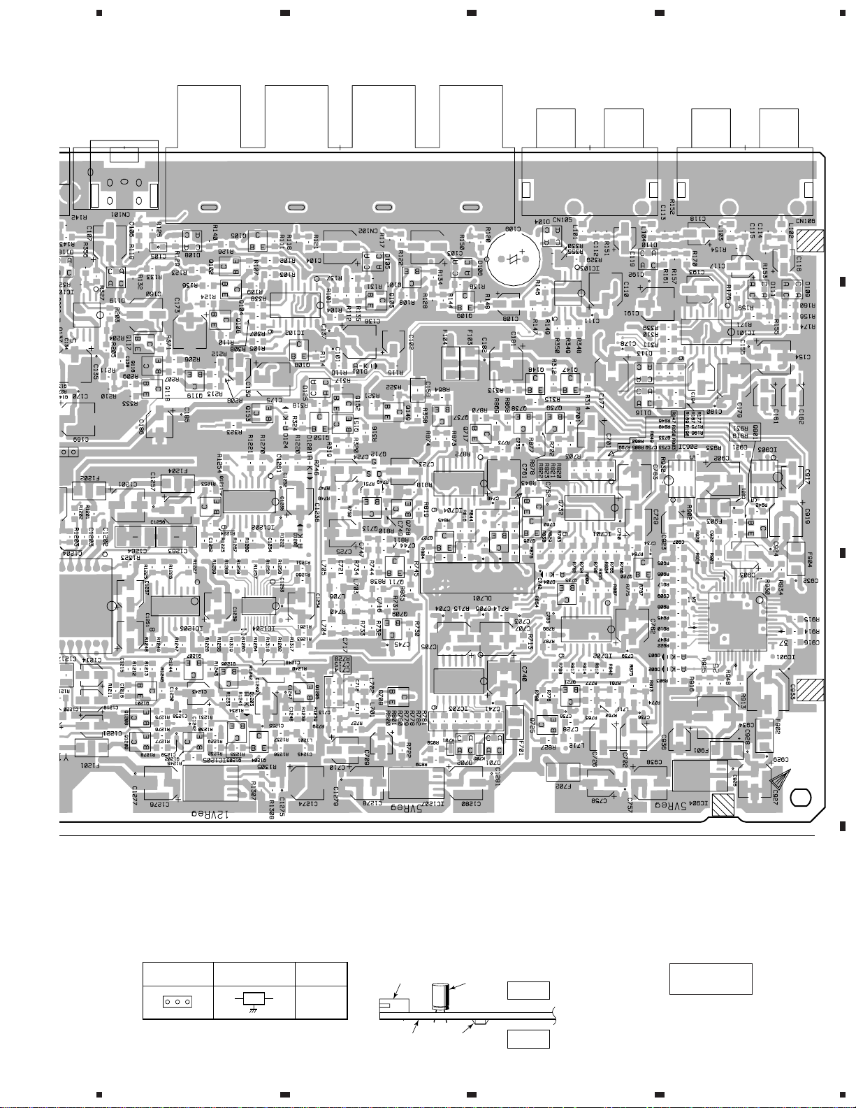
4. PCB CONNECTION DIAGRAM
VIDEO ASSY
A
B
(ANP1942–B)
C
D
CN503
CN304
A30
PDP-502MXE
VIDEO ASSY
SIDE A
A31
Q120Q1212–Q1214
Q121
Q122
Q141
NOTE FOR PCB DIAGRAMS:
1. Part numbers in PCB diagrams match those in the schematic
diagrams.
2. A comparison between the main parts of PCB and schematic
diagrams is shown below.
Symbol in PCB
Diagrams
BCE
BCE
Symbol in Schematic
Diagrams
BCE
BCEBCE
IC106
BCE
Q114
Q1215–Q1217
IC1208
Part Name
Transistor
Transistor
with resistor
Q115
Q1210
Symbol in PCB
Diagrams
DGS
IC108
Q1229
Symbol in Schematic
Diagrams
DGSDGS
Q1220
Q135–Q140
IC1201
Q1219
Part Name
Field effect
transistor
Resistor array
IC104
16
1234
Page 45

5
67
8
PDA-5001
A
B
IC104
Q104
Q102
Q116–Q119
IC1203
Symbol in PCB
Diagrams
3. The parts mounted on this PCB include all necessary parts
for several destination.
For further information for respective destinations, be sure
to check with the schematic diagram.
Q106
Q1211
Q1201–Q1209
Symbol in Schematic
Diagrams
IC1202
IC1204
IC102
Q108
Q149–Q153
Part Name
3-terminal
regulator
5
Q103 Q101
Q713
Q728
Q711
Q709
4. Viewpoint of PCB diagrams
Q727
Q708
P. C. Board Chip Part
6
Q109
IC704
IC703
C
IC103
Q148
Q717Q737
Q738
Q732
Q726
Q725
Q739
Q735
Q147
IC701
Q720
Q721
IC902
IC101
IC903
Q901
IC901IC702
D
CapacitorConnector
SIDE A
SIDE A
SIDE B
17
7
8
Page 46

PDA-5001
A
VIDEO ASSY
B
1
234
C
Q110–Q113
Q903–Q905
Q919
Q729
Q731
Q918
Q723
Q915
Q154
Q722
Q924
Q146
Q730
Q145
Q736
Q734
Q714
Q716Q701–Q703
Q704–Q707
Q107
Q710
D
18
1234
Page 47

5
67
8
PDA-5001
SIDE B
A
B
Q131–Q134
Q1218
(ANP1942–B)
C
Q123–Q130
D
19
5
6
7
8
Page 48

PDA-5001
5. PCB PARTS LIST
NOTES : ÷ Parts marked by “ NSP ” are generally unavailable because they are not in our Master Spare Parts List.
÷ The
÷ When ordering resistors, first convert resistance values into code form as shown in the following examples.
mark found on some component parts indicates the importance of the safety factor of the part.
Therefore, when replacing, be sure to use parts of identical designation.
Ex. 1 When there are 2 effective digits (any digit apart from 0), such as 560 ohm and 47k ohm (tolerance is shown by
J = 5%, and K = 10%).
560 Ω = 56 × 10
47k Ω = 47 × 10
1
= 561................................................... RD1/4PU 5 6 1 J
3
= 473 .................................................. RD1/4PU 4 7 3 J
0.5 Ω = R50 ...................................................................... RN2H Â 5 0 K
1 Ω = 1R0 ......................................................................... RS1P 1 Â 0 K
Ex. 2 When there are 3 effective digits (such as in high precision metal film resistors).
1
5.62k Ω = 562 × 10
= 5621 ........................................... RN1/4PC 5 6 2 1 F
Mark No. Description Part No.
VIDEO ASSY
SEMICONDUCTORS
IC1208 24LC64(I)SN
IC105, IC106, IC703 CXA1875AM
IC901 CXD2064Q
IC103, IC104 MC14577CF
IC902, IC903 ML6428CS-1
IC1203 NJM319M
IC1207, IC904 PQ05TZ51
IC1205, IC1206 PQ20VZ1U
IC1201 TB1227BN
IC101, IC102, IC702 TC4052BF
IC108, IC701, IC704 TC4053BF
IC107 TC74HC02AF
IC1202 TC74HC4538AF
IC1204 TC74VHCT541AFT
Q116, Q1208–Q1210, Q1215–Q1218 2SA1162
Q123–Q130, Q135–Q138, Q141 2SA1162
Q149, Q153, Q711, Q716–Q719 2SA1162
Q727, Q731, Q733, Q739 2SA1162
Q101–Q113, Q117–Q120 2SC2712
Q1201–Q1207, Q121, Q1211–Q1214 2SC2712
Q1219, Q122, Q1220, Q1221 2SC2712
Q139, Q140, Q147, Q148 2SC2712
Q150–Q152, Q701–Q710 2SC2712
Q713–Q715, Q720, Q726 2SC2712
Q728, Q729, Q732, Q735, Q736 2SC2712
Q738, Q901, Q903–Q905 2SC2712
Q114, Q115 2SC4213
Q712 2SK208
Q145, Q146, Q722–Q725, Q730 DTC124EK
Q734, Q737 DTC124EK
Q131–Q134 DTC143EK
D102–D120, D1204–D1206 1SS226
D1209–D1214, D125–D127 1SS226
D701, D702 1SS226
D101, D1201–D1203, D1207, D1208 1SS352
D121, D122, D124, D128 1SS352
D703, D704, D901–D903 1SS352
Mark No. Description Part No.
COILS AND FILTERS
F101–F104, F1201–F1204 ATF1189
F701, F702, F901–F904 ATF1189
DL701 ATN1045
L702 LCTA120J3225
L101–L107, L110 LCTA1R0J3225
L710 LCTA1R8J3225
L711, L716 LCTA270J3225
L708, L709 LCTA3R9J3225
L703, L707, L712, L715, L717 LCTA470J3225
L108, L109, L1201 LCTA560J3225
L706 LCTA5R6J3225
L701, L704 LCTA6R8J3225
L705 LCTA8R2J3225
CAPACITORS
C1263, C1264 (0.47 µF/16V) ACE1130
C1227 CCSQCH120J50
C1293, C713, C717 CCSQCH121J50
C716 CCSQCH151J50
C718 CCSQCH181J50
C730 CCSQCH220J50
C1262, C712, C719, C720 CCSQCH221J50
C728, C732 CCSQCH270J50
C1245, C1246, C721 CCSQCH271J50
C727 CCSQCH470J50
C1234, C1261 CCSQCH471J50
C731 CCSQCH560J50
C711 CCSQCH821J50
C1215 CCSQSL102J50
C714 CCSQSL122J50
C109, C133 CEAT102M10
C1228, C1243, C1249, C145, C709 CEV100M16
C724 CEV100M16
C1282 CEV101M16
C740, C902, C919, C927 CEV101M6R3
C1218, C1220, C1221, C1248, C917 CEV1R0M50
C923 CEV1R0M50
C1236, C1237, C1239, C1251, C1256 CEV220M16
C1292, C144, C701, C702, C726 CEV220M16
C729, C758, C903 CEV220M16
20
Page 49

PDA-5001
Mark No. Description Part No. Mark No. Description Part No.
C108, C139, C936 CEV220M6R3
C933, C934 CEV221M10
C1214, C1233 CEV2R2M50
C710, C725 CEV330M10
C103, C104, C107, C110, C1201 CEV470M16
C1206, C1209, C1225, C1229 CEV470M16
C1265–C1269, C1274, C1276, C1278 CEV470M16
C1280, C1284, C1288, C1294, C134 CEV470M16
C136, C140–C143, C154, C165 CEV470M16
C167, C169, C171, C173, C175 CEV470M16
C177, C179, C181, C191, C705 CEV470M16
C707, C761–C763, C938 CEV470M16
C1254, C1290, C183, C184 CEV470M6R3
C186–C188 CEV470M6R3
C102, C116–C119, C1210, C1223 CEV4R7M35
C123–C125, C127, C1283, C129 CEV4R7M35
C131, C146, C161, C162 CEV4R7M35
C193, C194, C723 CEVNP100M16
C160 CEVNP470M6R3
C1211–C1213, C1217, C1222, C158 CFHSP104J16
C105, C1219, C1224, C1231 CFHSQ103J16
C913 CKSQYB102K50
C1202–C1205, C1207, C1208, C1226 CKSQYB103K50
C1230, C132, C138, C147, C148 CKSQYB103K50
C150, C708, C722, C747 CKSQYB103K50
R327–R330 RS1/10S4700F
R1308 RS1/10S4701F
R1304 RS1/10S6201F
R207, R333 RS1/10S6800F
R117, R118, R142, R214, R216 RS1/10S75R0F
R218, R220 RS1/10S75R0F
R318, R355 RS1/10S8201F
R332 RS1/2S750J
Other Resistors RS1/10S J
OTHERS
CN103, CN104 CONNECTOR AKP1003
CN101 SOCKET AKP7045
CN102 CONNECTOR AKX1053
K701, K702 AKX9002
X1201 (16.2 MHz) ASS1152
CN1201 CONNECTOR B13B-PH-SM3
CN1202 CONNECTOR B8B-PH-SM3
CN105, CN106 JACK DKB1031
C904–C912, C914, C915, C920 CKSQYB103K50
C935 CKSQYB103K50
C1216, C1232, C1240, C1241, C751 CKSQYB104K25
C921, C922 CKSQYB104K25
C112–C115, C120–C122, C126 CKSQYB222K50
C128, C130 CKSQYB222K50
C916 CKSQYB223K50
C715 CKSQYB392K50
C106 CKSQYB473K50
C101, C111, C1235, C1238, C1242 CKSRYF104Z16
C1244, C1247, C1250, C1252, C1253 CKSRYF104Z16
C1255, C1257–C1260, C1270, C1273 CKSRYF104Z16
C1275, C1277, C1279, C1281, C1285 CKSRYF104Z16
C1289, C1291, C1295, C135, C137 CKSRYF104Z16
C149, C151–C153, C155, C159 CKSRYF104Z16
C166, C168, C170, C172, C174 CKSRYF104Z16
C176, C178, C180, C182, C185 CKSRYF104Z16
C189, C190, C192, C703, C704 CKSRYF104Z16
C706, C733–C739, C741–C746 CKSRYF104Z16
C748–C750, C752–C757 CKSRYF104Z16
C759, C760, C901, C918 CKSRYF104Z16
C924–C926, C928–C932, C937 CKSRYF104Z16
RESISTORS
R1305, R1306 RS1/10S1001F
R317 RS1/10S1801F
R266 RS1/10S1802F
R267, R331 RS1/10S2401F
R1307, R356 RS1/10S3901F
21
Page 50

PDA-5001
6. ADJUSTMENT
It is necessary to install VIDEO BOX PDA-5001 in Plasma Display PDP-502MXE to carry out the adjustment. Adjust PDA-5001 with
"VIDEO BOX" mode in Service Factory Mode of PDP-501MXE. Refer to Service Manual of PDP-502MXE/YVLDK (Order No.
ARP3037) for the details of Service Factory Mode.
Adjustment of PDA-5001 is necessary in order to supply decoded RGB signals at standard level to PDP-502MXE.
VIDEO BOX mode (Adjustment is independent of each signal)
Adjustment data is stored in EEPROM of VIDEO ASSY within Video Box.
Remote
Control
Key
1 CONTRAST Gain adjustment Adjustment required –––
2 BRIGHT Offset adjustment Adjustment required
3 COLOR Color Level adjustment Adjustment required –––
4 TINT Tint setting 64 ––– ––– 64 –––
5 RGB CONTRAST Gain adjustment ––– ––– ––– –––
6 Y DELAY Y-C Delay Setting 2 0 3 0 –––
7 R GAIN Adjustment required
8 B GAIN Adjustment required
9 R-Y OFFSET Adjustment required –––
10 B-Y OFFSET Adjustment required –––
11 COLOR (Y MUTE) Color Level adjustment The same data as 3 –––
12 TINT (Y MUTE) Tint setting The same data as 4 –––
Adjustment
Parameter
Adjusting & Setting Item
NTSC PAL SECAM 4.43NTSC SCART RGB
Gain adjustment
Offset adjustment
Setting Value
Adjustment required
Adjusting Method
Waveform observing point: CN1201 VB1 RGB output (Pin1: R, Pin 3: G, Pin 5: B)
Procedure
Adjusting Item Input signal Adjusting Point Adjusting Method
Offset adjustment
1
VIDEO BOX in
Factory mode
BRIGHT….…"2" Key
R-Y OFFSET….…
"9" Key
B-Y OFFSET….…
"10" Key
B.B signal
or
GRAY SCALE
(No SETUP)
BRIGHT….…"2" Key
Adjust to match Blanking level and Signal 0% level at each RGB
output.
At this time, deviation among R,G, and B must be within 10mV.
Be careful of the deviation because G-output also varies in the ratio
shown in the following table when OFFSET data is changed.
BRIGHT 1 1 1
R-Y OFFSET 1 – 0.5 0
B-Y OFFSET 0 – 0.2 1
Match BLK period
In SCART RGB signal input, only BRIGHT is used and adjust to
match Blanking level and G-output 0% level.
RGB
BLK period
22
Page 51

PDA-5001
Procedure
2
3
Adjusting Item Input signal Adjusting Point Adjusting Method
Gain adjustment
Color Level
adjustment
White 100%
signal
or
GRAY SCALE
(1 Vp-p)
(In SCART RGB
signal : 0.7 Vp-p)
75% Color bar
signal
VIDEO BOX in
Factory mode
CONTRAST ….…
"1" Key
R GAIN ….………
"7" Key
B GAIN ….………
"8" Key
RGB CONTRAST
….……… "5" Key
VIDEO BOX in
Factory mode
COLOR (Y MUTE)
….……… "11" Key
or
COLOR ….………
"3" Key
Adjust so that 0% to 100% level at each RGB output becomes
1.4Vp-p.
At this time, deviation among R,G,B must be within 30 mV.
1.4 Vp–p
In SCART RGB signal input, adjust them using RGB CONTRAST
instead of CONTRAST.
Adjust so that R-Y color-difference signal level at R-output becomes
1.4Vp-p ± 0.05V with remote control key.
1.4 Vp–p
Adjust it with key "3" when adjustment with LD pictures is required.
23
Page 52

PDA-5001
7. GENERAL INFORMATION
7.1 CONNECTION AND DISASSEMBLY
Connecting this unit to the display
This unit is to be used only when connected to the plasma
display, PDP-502MXE.
Before connecting this unit to the display, please be
sure to do the following:
÷ Undo any component or personal computer connections that
may have already been made to the plasma display.
÷ Make sure that the power of the plasma display is turned off, and
is unplugged from the wall outlet.
Precautions when connecting this unit to the display
When the covers on this unit and/or the display are opened to make
connections, be sure to avoid letting the screw rivets or their
respective parts fall into openings on the units. When connecting
(this unit) to the plasma display, always install with the display
upright. Dropping a screw or rivet into the display may damage it.
3 Separate the two connector cables from the cover.
4 Pull the two connector cables through the slot on the connector
cover included with this unit.
CAUTION
This unit is designed only for connection to the plasma display,
PDP-502MXE. Do not alter or modify this unit in any way as it may
cause this unit to perform abnormally and/or may cause the plasma
display to malfunction.
To connect this unit to the plasma display PDP- 502MXE
1 Remove the cover plate on the back panel of the plasma display.
Unscrew using a philips
screwdriver (“+” head).
Note:
If for some reason the screws cannot
be unscrewed, use a tool or other
object with a tip flat enough to fit
between the screw and rivet and pry
the screw out as shown below.
Connector Cover
(PDP-502MXE side)
2 Remove the cover plate on the back panel of the plasma display.
The two cable connectors are attached to the inside of the cover
plate.
J123
8P Wire Assy
(ADX2554)
J122
13P Wire Assy
(ADX2553)
Connector Cover
(Included with this unit)
5 Secure the connector cover onto the display with 2 of the
included screw rivets.
Screw Rivet
24
Page 53

PDA-5001
6 Remove the cover on this unit.
When the cover is removed, the two connector terminals should
be clearly visible.
Screw Rivet
7 Align the holes on this unit with the corresponding holes on the
rear panel of the plasma display and secure this unit to the
plasma display using 4 of the included screw rivets.
2
3
1
4
8 Connect the connector cables to the respective terminals located
on the inside of this unit.
Make sure that connections are made correctly and securely.
J122
13P Wire Assy
(ADX2553)
J123
8P Wire Assy
(ADX2554)
CN1201 VB1
(PDA-5001 side)
CN1202 VB2
(PDA-5001 side)
9 Replace the cover of this unit.
Connection of this unit is complete.
PDP-502MXE
÷ When aligning this unit with the plasma display, be sure to bring
the two connector cables through this unit.
÷ Attach the screw rivets in the numbered order shown above. The
procedure for attaching the screw rivets is described in step 5.
÷ When connecting this unit to the plasma display, make sure that
the cable connectors are not pinched between the two units.
Disassembling the unit from the display
To remove this unit from the display, take the above steps in
reverse order.
25
Page 54

PDA-5001
8. PANEL FACILITIES AND SPECIFICATIONS
PANEL FACILITIES
123
R
SPEAKER
8 Ω – 16 Ω
+–
AUDIO OUTPUT
IN
OUT
COMBINATION
IN
CONTROL
OUT
RS-232C
4-098765
1 AUDIO INPUT (Pin jacks)
Use to obtain sound when INPUT2 (BNC/S) is selected.
Connect the audio output jack of components connected
to INPUT2 (BNC/S) to these jacks.
2 AUDIO INPUT (Pin jacks)
Use to obtain sound when INPUT1 (BNC) is selected.
Connect the audio output jack of components connected
to INPUT1 (BNC) to these jacks.
3 INPUT1 (BNC)
For connection of components that have a composite
video output jack.
Use the INPUT1 OUT jack to output the video signal to an
external monitor or other component.
Note: The video signal will not be output from the INPUT1
OUT jack when the main power of the plasma display is
off or in standby mode .
4 SPEAKER (R) terminal
For connection of an external right speaker.
Connect a speaker whose impedance is 8 -16 Ω.
5 AUDIO OUTPUT (Stereo mini jack)
Use to output the audio of the selected source component
connected to this unit.
6 COMBINATION IN/OUT
DO NOT MAKE ANY CONNECTIONS TO THESE
TERMINALS.
These terminals are used in the factory setup.
(INPUT 4)
AUDIO INPUT
R – L
(INPUT 3)
ANALOG
R G B
INPUT4
OUTPUT
ANALOG
(
R G B
(
7 CONTROL IN/OUT
For connection of PIONEER components that bear the Î
mark. Making CONTROL connection enables control of this
unit as a component in a system.
8 RS-232C
DO NOT MAKE ANY CONNECTIONS TO THIS
TERMINAL.
This terminal is used in the factory setup.
9 AUDIO INPUT (Stereo mini jack)
Use to obtain sound when INPUT4 is selected.
Connect the audio output jack of components connected
to INPUT4 to this jack.
0 AUDIO INPUT (Pin jacks)
Use to obtain sound when INPUT3 is selected. Connect
the audio output jack of components connected to INPUT3
to these jacks.
Note: The left audio channel (L) jack is not compatible
with monaural input sources.
- INPUT4
For connection of a personal computer (PC) or similar
component. Make sure that the connection made
corresponds to the format of the signal output from the
connected component.
Use the INPUT4 OUTPUT terminal to output the video
signal to an external monitor or other component.
Note: The video signal will not be output from the INPUT4
OUTPUT terminal when the main power of the plasma
display is off or in standby mode .
26
Page 55

PDA-5001
=~ !@
GBR
[ON SYNC] [H/V SYNC]
INPUT3
HD VD
75Ωj2.2kΩ
$%^&#
= INPUT2 (BNC/S)
For connection of components that have an S-video output
jack or Y/C separate video output jacks.
Note: Do not use both the S-VIDEO jack and the BNC
jacks in parallel. Doing so may cause this unit to
malfunction or become damaged.
~ INPUT2 (SCART)
For connection of a VCR or similar component compatible
with SCART connections.
! INPUT1 (SCART)
For connection of an A V component compatible with SCART
connections.
@ Video box connection cover
Remove when connecting this unit to the plasma display,
PDP-502MXE.
# INPUT3
For connection of components that have RGB or
component output jacks such as a personal computer , DVD
player, or external RGB decoder.
MAIN POWER
OFF ON
AC INLET
SPEAKER
8 Ω – 16 Ω
+–
L
$ Synchronizing signal impedance selector switch
Depending on the connections made at INPUT3, it may
be necessary to set this switch to match the output
impedance of the connected component’ s synchronization
signal.
When the output impedance of the component’s
synchronization signal is above 75 Ω, set this switch to
the 2.2 kΩ position.
% MAIN POWER switch
Use to switch the main power of the unit on and off.
^ AC INLET
Use to connect a power cord to an AC outlet.
& SPEAKER (L) terminal
For connection of an external left speaker. Connect a
speaker that has an impedance of 8 -16 Ω.
27
Page 56

PDA-5001
SPECIFICATIONS
General
External dimensions......... 338 (W) x 156 (H) x 30 (D) mm.
(including monitor)......... 1218 (W) x 737 (H) x 128 (D) mm
Weight...................................................................... 1.1 kg
(including plasma display monitor) ........................ 41.4 kg
Operating temperature range ............................ 0 to 40 °C
Input/output
Video
INPUT1 (BNC)
Input BNC jack
÷ Composite video signal
1 Vp-p/75 Ω/negative sync.
Output BNC jack
75 Ω /with buffer
INPUT 2 (BNC/S)
Input 1 S terminal (Mini DIN 4 pin)
2 BNC jack (x2)
÷ Y/C separate video signal
Y . . . 1 Vp-p/75 Ω/negative sync.
C . . .0.286 Vp-p/75 Ω (NTSC)
0.3 Vp-p/75 Ω (PAL)
Audio
Input INPUT 1
Pin jack (x2)
L/R ... 500mVrms/more than 10 kΩ
INPUT 2
Pin jack (x2)
L/R ... 500mVrms/more than 10 kΩ
INPUT1 (SCART)
Input SCART jack
÷ Composite video signal
1 Vp-p/75 Ω/negative sync.
÷ RGB signal
0.7 Vp-p/75 Ω
÷ Audio L/R. . .500 mVrms/more than 10 kΩ
INPUT2 (SCART)
Input SCART jack
÷ Composite video signal
1 Vp-p/75 Ω/negative sync.
÷ Y/C separate video signal
Y . . . 1 Vp-p/75 Ω/negative sync.
C . . .0.3 Vp-p/75 Ω (PAL)
0.286 Vp-p/75 Ω (NTSC)
÷ Audio L/R. . .500 mVrms/more than 10 kΩ
Output
÷ Composite video signal
1 Vp-p/75 Ω/negative sync.
÷ Audio L/R. . .500 mVrms/less than 1 kΩ
Accessories
Pin/BNC conversion adaptor ............................................ 1
Screw rivets ..................................................................... 8
Connector cover............................................................... 1
Operating Instructions...................................................... 1
28
÷ Due to improvements, specifications and design are subject to
change without notice.
 Loading...