

Page 1
ORDER NO.
RRV2363
MINIDISC RECORDER
MJ-NS1
THIS MANUAL IS APPLICABLE TO THE FOLLOWING MODEL(S) AND TYPE(S).
Type
ZPWXJ DC power supplied from other system component
¶ This product is a system(s) component.
This product does not function properly independently ; to avoid malfunctions, be
sure to connect it to the prescribed system component(s), otherwise damage may
result.
¶ Please connect it to the STEREO CD TUNER XC-NS1 and STEREO POWER AMPLI-
FIER M-NS1 for adjustment and operation inspection.
Model
MJ-NS1
Power Requirement Remarks
Component Model Service manual Remarks
STEREO CD TUNER XC-NS1 RRV2348 (RRV2341)
STEREO POWER AMPLIFIER M-NS1 RRV2349 (RRV2321)
SPEAKER SYSTEM S-NS1-LRW RRV2371 Except YPWXJ type
MINIDISC RECORDER MJ-NS1 RRV2363 This manual.
CONTENTS
1. SAFETY INFORMATION
2. EXPLODED VIEWS AND PARTS LIST
3. BLOCK DIAGRAM AND SCHEMATIC DIAGRAM
4. PCB CONNECTION DIAGRAM
5. PCB PARTS LIST
6. ADJUSTMENT
PIONEER CORPORATION 4-1, Meguro 1-chome, Meguro-ku, Tokyo 153-8654, Japan
PIONEER ELECTRONICS SERVICE, INC. P.O. Box 1760, Long Beach, CA 90801-1760, U.S.A.
PIONEER EUROPE NV Haven 1087, Keetberglaan 1, 9120 Melsele, Belgium
PIONEER ELECTRONICS ASIACENTRE PTE. LTD. 253 Alexandra Road, #04-01, Singapore 159936
c
PIONEER CORPORATION 2000
....................................................
.........................................................
...........................................
.....................
.....
...............................
7. GENERAL INFORMATION
2
7.1 DIAGNOSIS
3
8
21
26
29
7.1.1 SINGLE OPERATION METHOD
7.1.2 POWER ON SEQUENCE
7.1.3 DISASSEMBLY
7.2 IC
8. PANEL FACILITIES AND SPECIFICATIONS
...................................................................
...................................................
T – ZZV AUG. 2000 Printed in Japan
..................................
............
.......................
.......................................
......
37
37
37
38
40
43
46
Page 2
MJ-NS1
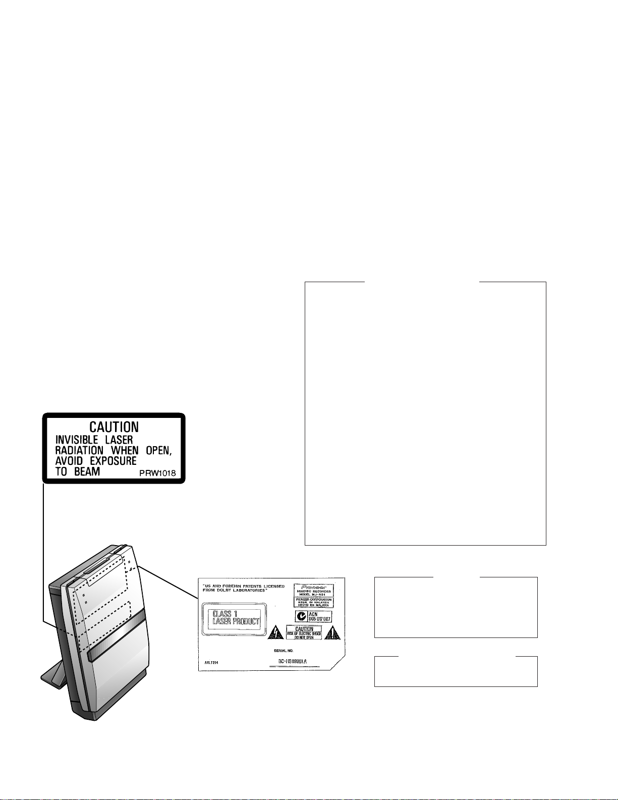
1. SAFETY INFORMATION
This service manual is intended for qualified service technicians; it is not meant for the casual
do-it-yourselfer. Qualified technicians have the necessary test equipment and tools, and have been
trained to properly and safely repair complex products such as those covered by this manual.
Improperly performed repairs can adversely affect the safety and reliability of the product and may
void the warranty. If you are not qualified to perform the repair of this product properly and safely, you
should not risk trying to do so and refer the repair to a qualified service technician.
Additional Laser Caution
Control method of the current through a laser diode.
The resistor R105 on the CORE MAIN UNIT ASSY (For MD
mechanism assy) are for the limiting of current through a laser
diode.
LABEL CHECK
Control method of the laser output power
The laser pickup assy provide the photo-diodes and APC (Auto
Power Control) circuit.
The photo-diode detect output of the laser diode then IC104 control
the APC circuit according to the signal voltage of the photo-diode via
IC101.
The Variable resistancer on the FPC in the Laser pickup assy can
be adjusted the output level of Laser diode to fix the rated output
level.
Laser Interlock Switch
The loading position detect switch S101 is set to “ LOAD ON ” (ON:
low level, OFF: high level) position, IC104 get the “ LOAD ” signal,
and hand the laser “ LDON ” signal to No. 9 terminal (LDON) of the
Laser pickup assy.
Then a laser diode can be lighted exept when the level of signal
“LOAD ” is low.
∗ Refer to page 30.
IMPORTANT
THIS PIONEER APPARATUS CONTAINS
LASER OF CLASS 1.
SERVICING OPERATION OF THE APPARATUS
SHOULD BE DONE BY A SPECIALLY
INSTRUTED PERSON.
LASER DIODE CHARACTERISTICS
MAXIMUM OUTPUT POWER: 32 mW
WAVELENGTH: 785 nm
2
Page 3
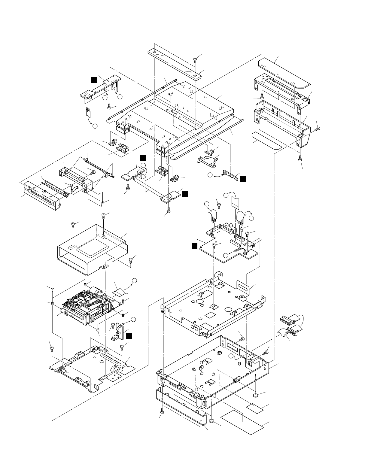
2. EXPLODED VIEWS AND PARTS LIST
NOTES:• Parts marked by "NSP" are generally unavailable because they are not in our Master Spare Parts List.
The mark found on some component parts indicates the importance of the safety factor of the part.
•
Therefore, when replacing, be sure to use parts of identical designation.
Screws adjacent to mark on the product are used for disassembly.
•
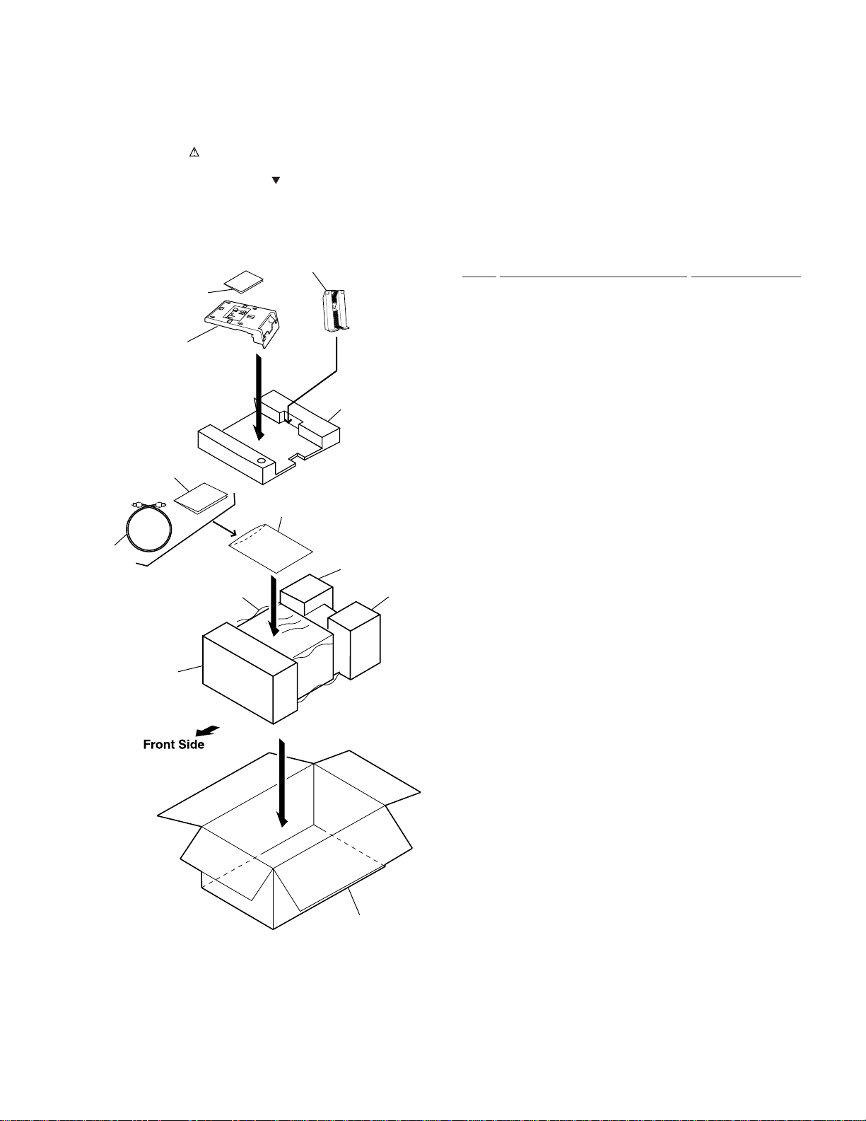
2.1 PACKING
(1) PACKING PARTS LIST
3
Mark No. Description Part No.
MJ-NS1
8
2
6
7
10
1
11
12
13(1/2)
13(2/2)
NSP 8 Warranty Card ARY7027
NSP 10 Polyethylene Bag Z21-038
1 Optical Digital Cable RKX1031
2 Stand A AXG7096
3 Stand B AXG7097
4 • • • • • • •
5 • • • • • • •
6 Spacer MD ,TC AHB7038
7 Operating Instructions ARE7266
(English/Chinese)
9 • • • • • • •
(230×340×0.03)
11 Sheet (550×550×0.5) Z23-026
12 Front Pad M (PLS) AHA7295
13 Rear Pad M (PLS) AHA7296
14 Packing Case AHD7901
14
3
Page 4
MJ-NS1
2.2 EXTERIOR
30
26
12
18
37
38
19
E
A
2
27
22(1/2)
32
23
31
C
B
38
3
D
A
27
14
22(2/2)
38
37
38
13
4
C
1
34
29
17
B
E
38
C
38
38
31
36
5
F
F
37
38
24
25
38
28
16
39
A
37
D
20
21
7
" Refer to
2.3 MD Mechanism"
38
21
21
37
8
21
E
20
D
6
10
38
B
38
11
38
24
F
15
38
15
40
35
9
33
4
Page 5

EXTERIOR PARTS LIST
Mark No. Description Part No.
MJ-NS1
NSP 2 RELAY UNIT AWU7576
NSP 3 KEY L UNIT AWU7577
NSP 4 KEY R UNIT AWU7652
NSP 5 BLUE UNIT AWU7653
NSP 6 IC UNIT AWU7654
NSP 7 MD Mechanism AXA7087
NSP 10 Bottom Chassis MDTC ANA7108
1 MAIN UNIT AWU7607
8 Lead Card 30P (J4101) ADD7280
(MAIN CN4101 ↔ MD CORE CN104)
9 Cord with Plug (J4103) ADE7065
(System Cable to CD Receiver)
11 Sub Chassis (MTL) AND7036
12 Disc Guard (MTL) ANG7319
13 Shield Case (FE) ANK7077
14 MD Spring ABH7189
15 Leg AEB7090
16 FL Holder (PLS) AMR7312
17 Illumination Holder AMR7317
18 MD Flap Holder (PLS) AMR7318
19 MD Cam (PLS) AMR7319
20 Float Screw (FE) RBA1133
21 Float Rubber (Rubber) REB1328
22 Button MD (PLS) AAD7582
23 Display Window MD (PLS) AAK7763
24 Rear Cap MD TC (PLS) AAK7772
25 FL window MD TC (PLS) AAK7793
26 Door NS (PLS) AAK7807
27 Lens MD TC (PLS) AAK7838
28 FL Cover AAK7841
29 Illuminate Lens (PLS) AAK7842
30 Sub Panel MD (PLS) AAP7069
31 Side Line (PLS) AAP7074
32 Screw (Steel) ABA7062
33 Bottom Base CDMD (PLS) AMA7017
NSP 35 Name Label (PAP) MD/ZP AAL7254
34 Top Panel MD (PLS) AMB7700
36 Connector Label ARW7110
37 Screw BBZ30P080FMC
38 Screw BBZ30P080FZK
39 Screw VBZ30P100FZK
40 Caution Label PRW1018
5
Page 6
MJ-NS1
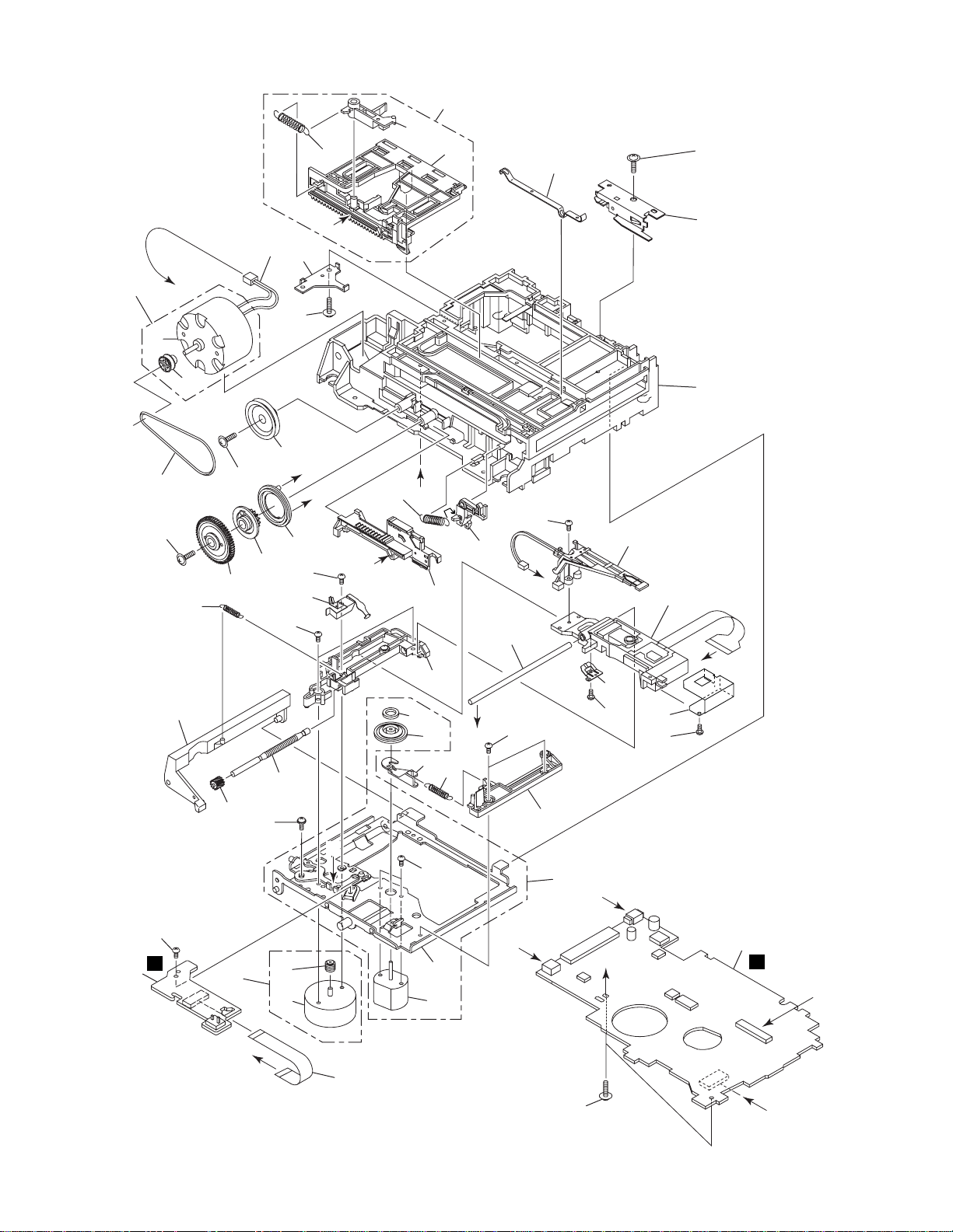
2.3 MD MECHANISM
19
21
18
20
37
6
51
52
8
37
34
E
4
9
17
A
54
53
24
14
37
13
12
40
15
40
26
E
F
5
G
41
16
35
F
11
B
27
10
36
C
28
44
33
31
23
40
H
25
39
29
3946
32
42
30
H
38
43
B
CN102
40
H
2
48
49
50 47
45
A
CN105
G
1
G
C
CN101
D
3
54
6
CN103
D
Page 7

MD MECHANISM PARTS LIST
MJ-NS1
Mark No. Description Part No.
1 MD CORE MAIN UNIT AWU7591
NSP 2 MD CORE SW UNIT AWU7592
3 Lead Card 7P RDD1403
4 Lead Wire 2P RKP1814
5 Lever Spring RBH1463
6 Clamp Spring RBK1074
7 • • • • • • • • • •
8 Loading Belt REB1329
9 Lock Plate RNE1949
10 Loading Base (ABS) RNK2323
11 Under Slider (POM) RNK2314
12 Gear Pulley (POM) RNK2316
13 Drive Gear (POM) RNK2317
14 Clutch Gear (POM) RNK2318
15 Flip Disk (POM) RNK2319
16 SW Lever RNK2320
17 Shutter Assy (FE) RXA1774
NSP 18 Upper Slider Assy RXA1782
19 Eject Spring RBH1461
20 Upper Slider (POM) RNK2324
21 Carrier (POM) RNK2315
22 • • • • • • • • • •
23 Spindle Spring RBH1460
24 Lifter Spring RBH1462
25 Screw Guide (SUS) RBK1072
26 S.H. Spring (SUS) RBK1073
27 Guide Shaft RLA1312
28 Lead Screw (SUS) RLA1311
29 Shield Case (FE) RNE1950
30 Reference Plate RNK2306
Mark No. Description Part No.
31 S. Holder RNK2307
32 Worm Wheel RNK2309
33 Hook (POM) RNK2310
34 Head Lifter RNK2311
35 MD Head RPB1063
36 MD Pick-Up RWY1019
37 Screw (FE) Z39-019
38 Screw JFZ17P020FZK
39 Screw JGZ14P020FMC
40 Screw JGZ17P028FMC
41 Screw JGZ17P040FMC
42 Screw PMB20P040FMC
43 Servo Base Assy REA1283
NSP 44 Clamp Magnet RMF1002
NSP 45 Servo Base RNE1951
NSP 46 Disk Table RNK2305
NSP 47 Spindle Motor RXM1091
48 Carriage Motor Assy REA1284
49 Worm RNK2308
NSP 50 Carriage Motor RXM1090
51 Loading Motor Assy REA1290
52 DC Motor /0.75W PXM1010
53 CA Pulley RNK2322
54 Screw BPZ20P080FMC
7
Page 8
1
23
MJ-NS1
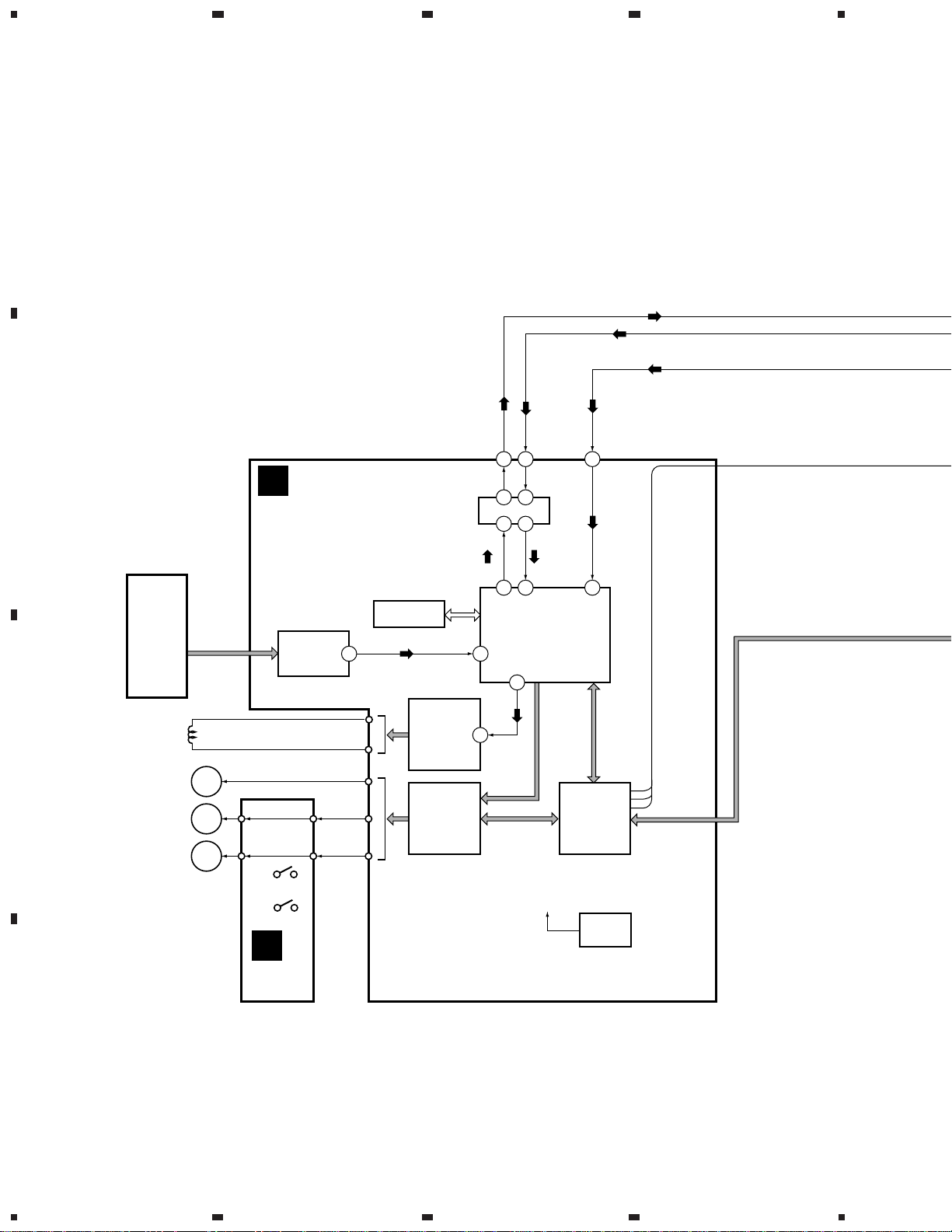
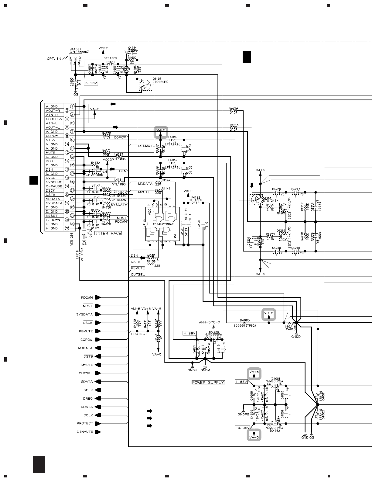
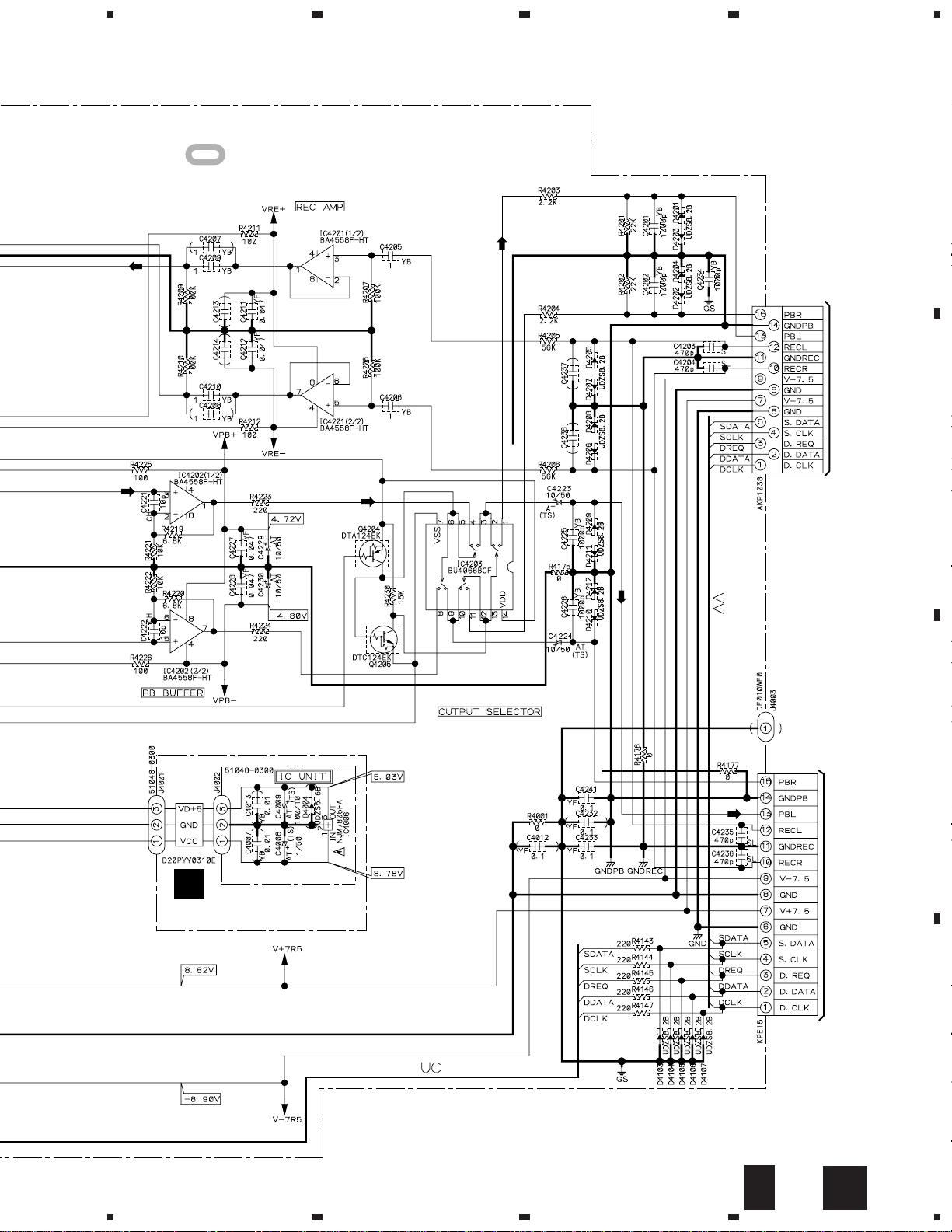
3. BLOCK DIAGRAM AND SCHEMATIC DIAGRAM
A
3.1 BLOCK DIAGRAM
(REC)
(MD)
AOUT-L
B
CN104
MD CORE MAIN UNIT
G
IC110
(AK4519VF)
Audio Codec
AIN-L
25 26
19 6
15 12
DIN
15
(D) (D)
4
(MD)
(REC)
(D)
IC103
(MSM51V4400D70TSK)
DRAM
MD PICKUP
REC HEAD
CN101
C
LOADING
CARRIAGE
SPINDLE
M
M
M
IC101
(IR3R55M)
RF Amp.
CN701
DISC
INSIDE
40
CN102
CN105
CN103
(RF)
IC107
(BD7910FV)
Head
Driver
IC106
(M56788FP)
5ch Motor
Driver
(MD)
74 73
Encoder/Decoder
3
7
H
MD CORE
SW UNIT
(REC)
DADATA
ADDATA
IC102
(LR376487)
+
Digital Servo
50
(REC)
VD+3
DIN
66
IC104
(PD5593A)
MD Mecha
Control
IC106
(RN5RG32AA)
+3.2V Reg.
CONTROL
CONTROL
CN106
D
8
1234
Page 9
5
678
MJ-NS1
Note : When ordering service parts, be sure to refer to "EXPLODED VIEWS and P AR TS LIST" or "PCB PARTS LIST".
OPT
DIGITAL IN
JA4601
CN4103
To CD Receiver
10
13
12
15
CN4102
From Deck
10
13
12
15
A
CN4101
AOUT-L
6
AIN-L
5
DIN
16
(D)
(D)
(D)
DIN
DSTB
MDDATA
MUTE
(TC74HCT08AF)
3V → 5V CONVERTER
(MD)
IC4102
(BA4558F-HT)
(REC)
(D)
IC4201
REC AMP
IC4202
(BA4558F-HT)
PB BUFFER
6
39
PBL
RECL
1
3
System Control U-com
PBR
RECR
3
1
IC4101
(PDG257A)
SDATA
SCLK
DREQ
DDATA
DCLK
(REC)
A
1
(MD)
4
(BU4066BCF)
OUTPUT SELECTOR
MAIN UNIT
RECL
IC4203
PBL
2
3
V+7.5V
RECR
PBR
B
IC4006
(NJM7805FA)
5V REG.
IC UNIT
B
VD+5V
TEST3
CN4107
TEST1
CN4105
1 3 2 11 2 3 4 5
GNDD
GNDD
MECAH TEST
INPUT
+SEARCH
FF
–SEARCH
REW
TEST2
CN4106
P-ON
CN4104
J4901
Key Input
Q4906
EJECT
Q4901-
LED Driver
REC STOP PLAY/PAUSE
(MD)
: AUDIO SIGNAL ROUTE (MD)
(D)
: DIGITAL SIGNAL ROUTE
(REC)
: AUDIO SIGNAL ROUTE (REC)
KEY-R UNIT
C
MONO
REC
DIGITAL
PLAY
D
E
F
KEY-L UNIT
RELAY UNIT
BLUE UNIT
C
D
9
5
6
7
8
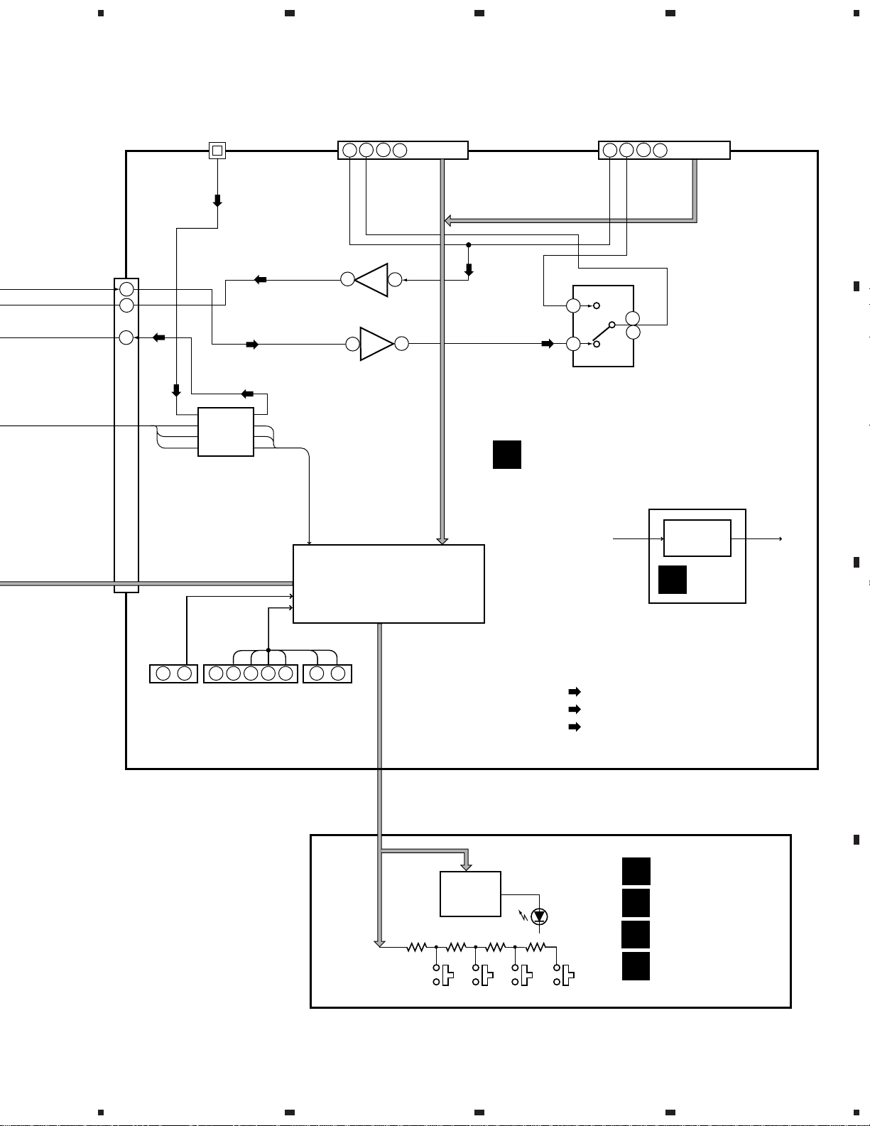
Page 10
1
23
MJ-NS1
3.2 OVERALL CONNECTION DIAGRAM
A
SHF
SHF
B
4
IC UNIT
(AWU7654)
B
G
C
MD CORE
SW UNIT
(AWU7592)
MD CORE MAIN UNIT
(AWU7591)
H
KEY-R UNIT
(AWU7652)
D
10
1234
C
Page 11
5
678
MJ-NS1
A
A
MAIN UNIT (AWU7607)
B
C
5
KEY-L UNIT
D
(AWU7577)
F
E
D
RELAY UNIT
(AWU7576)
6
7
BLUE UNIT
(AWU7653)
11
8
Page 12
1
MJ-NS1
3.3 MAIN UNIT (1/2)
A
CN104
B
G
(REC)
23
A
MAIN UNIT (1/2) (AWU7607)
(MD)
(D)
4
1/2
(MD)
CN4101
C
D
(D)
(MD)
: AUDIO SIGNAL ROUTE (MD)
(D)
: DIGITAL SIGNAL ROUTE
(REC)
: AUDIO SIGNAL ROUTE (REC)
3V-5V
Converter
12
1/2
A
1234
Page 13
5
678
MJ-NS1
(REC)
(MD)
: The power supply is shown with the marked box.
(MD)
(MD)
A
From DECK
B
CN4102
(MD)
B
IC UNIT (AWU7654)
5
C
(MD)
To CD RECEIVER
CN4103
1/2
A
6
7
B
8
13
D
Page 14
1
23
MJ-NS1
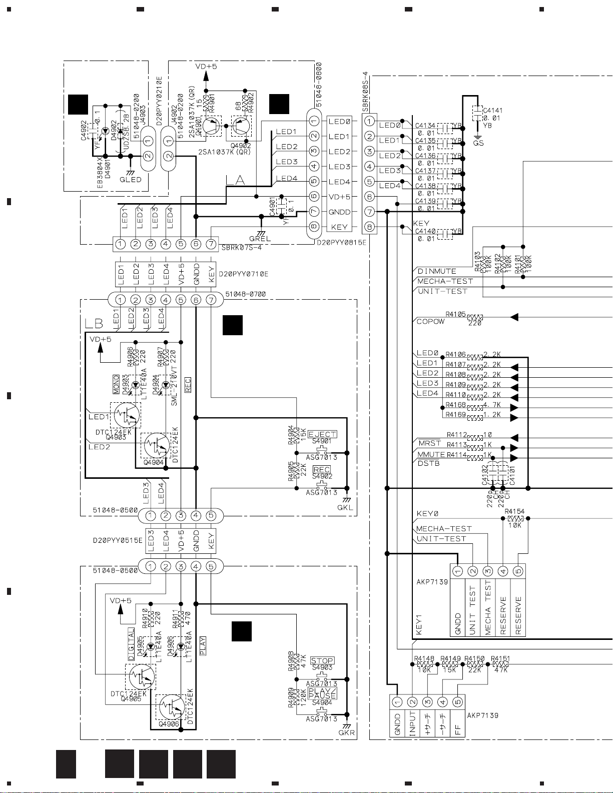
3.4 MAIN UNIT (2/2), KEY-R, KEY-L, RELAY and BLUE UNITS
4
BLUE UNIT
(AWU7653)
A
B
F
RELAY UNIT
(AWU7576)
CN4901
J4904
KEY-L UNIT
D
(AWU7577)
E
J4901
CN4104
SWITCHES
S4901 : EJECT
S4902 : REC
C
J4907
J4908
TEST3
CN4107
C
KEY-R UNIT
(AWU7652)
D
SWITCHES
S4903 : STOP
S4904 : PLAY/
PAUSE
14
2/2
A
1234
C
D
E F
TEST1
CN4105
Page 15
5
678
MJ-NS1
A
A
2/2
MAIN UNIT (2/2) (AWU7607)
B
SYSTEM CONTROL U-COM
C
TEST2
CN4106
5
D
2/2
A
6
7
8
15
Page 16

1
23
MJ-NS1
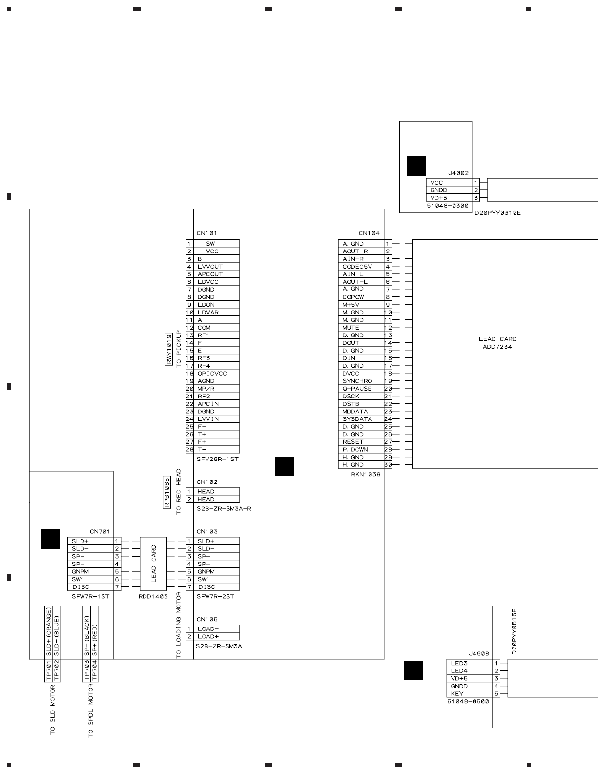
3.5 MD CORE MAIN and MD CORE SW UNITS
MD CORE MAIN UNIT
A
B
G
(AWU7591)
(RF)
(RF)
(RF)
(RF)
(RF)
(RF)
RF AMP
(RF)
(RF) (RF)
(RF)
(RF) (RF)
1
2
HEAD DRIVER
4
3
(RF)
(REC)
(REC)
(REC)
(REC)
(REC)
MD PICKUP
RWY1019
LOADING MOTOR
ASSY
REA1290
C
CARRIAGE MOTOR
ASSY
REA1284
SPINDLE
MOTOR
RXM1091
9
7
8
(REC)
(REC)
(REC)
5ch MOTOR DRIVER
H
MD CORE SW
UNIT
(AWU7592)
D
16
G
H
1234
Page 17

5
678
MJ-NS1
(RF)
: The power supply is shown with the marked box.
6
5
10
11
(MD)
(REC)
ENC/DEC
+
DIGITAL SERVO
DRAM (4M)
(D)
(CD)
4
(REC)
(D)
(D)
12
(RF)
: RF SIGNAL ROUTE
(D)
: DIGITAL SIGNAL ROUTE
(MD)
: AUDIO SIGNAL ROUTE (MD)
(REC)
: AUDIO SIGNAL ROUTE (REC)
(REC)
(REC)
(MD) (MD)
13
(REC)
14
AUDIO CODEC
(MD)
A
Not used
15
B
(REC)(REC)
10/16
C
REGULATOR
(+3.2V)
MD MECHA.
CONTROL µCOM
(D)
(D)
(D)
(D)
CN4101
1/2
A
EEPROM
(MD)
(REC)
D
G
5
6
7
8
17
Page 18

MJ-NS1
WAVEFOAM OF EACH PART
Note : The number with indicate the each measuring point number of the schematic diagram.
MD CORE MAIN UNIT
G
IC101 - pin 35 (ADIPO)
1
MODE: PLAY
DISC : GGF1328 (MMD–212)
V : DC500mV/div. H : 10µsec/div.
IC101 - pin 30 (WBO)
2
MODE: PLAY
DISC : GGF1328 (MMD–212)
V : DC1V/div. H : 10µsec/div.
GND
IC102 - pin 75 (FE MON)
5
MODE: PLAY
DISC : TGYS1 or MMD-110
V : DC100mV/div. H : 2msec/div.
Note : Connect the filter circuit below
at measuring.
FE MON
39 kΩ
To Oscilloscope
820pF
GND
CN103 - pin 1 (SLD +)
7
MODE: PLAY
V : DC500mV/div. H : 2msec/div.
CN103 - pin 4 (SP +)
8
MODE: PLAY
V : DC500mV/div. H : 5msec/div.
GND
IC102 - pin 1 (EFM MON)
3
MODE: PLAY
DISC : TGYS1 or MMD-110
V : DC500mV/div. H : 0.5msec/div.
IC102 - pin 50 (EFMO)
4
MODE: REC
DISC : GGF1277 or MMD-317
V : DC1V/div. H : 0.2µsec/div.
GND
GND
(MD Mechanism Assy TP)
IC102 - pin 77 (TE MON)
6
MODE: PLAY
DISC : TGYS1 or MMD-110
V : DC500mV/div. H : 2msec/div.
Note : Connect the filter circuit below
at measuring.
TE MON
REFO
39 kΩ
To Oscilloscope
820pF
GND
CN105 - pin 1 (LOAD –)
9
MODE: STOP
V : DC1V/div. H : 1msec/div.
MODE: EJECT
V : DC1V/div. H : 1msec/div.
GND
GND
18
GND
(MD Mechanism Assy TP)
REFO
GND
Page 19

MJ-NS1
IC102 - pin 74 (DADATA)
10
MODE: PLAY (1kHz 0dB)
DISC : TGYS1 or MMD-110
V : DC1V/div. H : 0.2µsec/div.
IC102 - pin 73 (ADDATA)
11
MODE: REC (ANALOG)
DISC : GGF1277 or MMD-317
V : DC1V/div. H : 0.2µsec/div.
GND
GND
IC110 - pin 11 (BCLK)
14
MODE: PLAY (1kHz 0dB)
DISC : TGYS1 or MMD-110
V : DC1V/div. H : 0.1µsec/div.
IC110 - pin 19 (OUTL)
15
MODE: PLAY (1kHz 0dB)
DISC : TGYS1 or MMD-110
V : DC500mV/div. H : 0.2msec/div.
GND
GND
IC110 - pin 9 (SYSCLK)
12
MODE: PLAY (1kHz 0dB)
DISC : TGYS1 or MMD-110
V : DC1V/div. H : 50nsec/div.
IC110 - pin 10 (LRCK)
13
MODE: PLAY (1kHz 0dB)
DISC : TGYS1 or MMD-110
V : DC1V/div. H : 5µsec/div.
GND
GND
19
Page 20

MJ-NS1
VOLTAGE OF EACH PART
MD CORE MAIN UNIT (1kHz 0dB PLAY)
G
IC101
Pin
Voltage
No.
1 0.78 25 2
2 0.73 26 0
3 0.77 27 1.4
4 0.75 28 1.42
5 1.61 29 1.4
6 1.61 30 1.63
7 0.75 31 1.61
8 1.61 32 1.61
9 1.61 33 0
10 1.61 34 0
11 1.61 35 0
12 1.61 36 1.62
13 3.19 37 0.59
14 3.19 38 1.61
15 0 39 1.61
16 0 40 1.61
17 3.19 41 1.61
18 0 42 3.19
19 0 43 0
20 1.5 44 1.08
21 3.2 45 1.61
22 0 46 1.61
23 0 47 0
24 3.19 48 0.74
Pin
(V)
No.
Voltage
IC102 IC103 IC104
Pin
Voltage
No.
(V)
1 1.53 51 1.59
2 3.18 52 0
3 1.65 53 0
4 0 54 1.59
5 1.42 55 1.8
6 0 56 0
7 1.59 57 0
8 1.41 58 0
9 1.97 59 0
10 1.39 60 0
11 1.64 61 0.56
12 3.18 62 3.18
13 0 63 0
14 0 64 1.5
15 0 65 1.5
16 0 66 3.2
17 1.69 67 1.6
18 1.52 68 0.96
19 1.7 69 0
20 1.47 70 1.6
21 1.47 71 1.6
22 1.65 72 1.48
23 1.54 73 0
24 1.69 74 0
25 1.51 75 1.68
26 0.82 76 1.82
27 2 77 1.59
28 2 78 0.35
29 1.81 79 0.02
30 1.4 80 3.2
31 0.82 81 3.2
32 1.67 82 0.02
33 1.67 83 0.03
34 1.67 84 1.9
35 2.86 85 1.56
36 1.32 86 3.1
37 2.23 87 3.2
38 0 88 0
39 2.4 89 3.19
40 1.2 90 0.5
41 1.5 91 0.5
42 0 92 0.5
43 2 93 0.5
44 3 94 0.9
45 1.2 95 0.5
46 1.2 96 0.5
47 0.02 97 0.5
48 3.04 98 0.8
49 1.57 99 3.18
50 0.05 100 0.06
Pin
(V)
No.
Voltage
(V)
Pin
Voltage
No.
(V)
1 1.2
2 1.2
33
42
5 1.45
678-
9 1.80
10 0.8
11 2.36
12 1.21
13 3.18
14 1.21
15 2.45
16 1.26
17 1.65
18 1.32
19 20 21 22 2.23
23 2.4
24 1.2
25 1.2
26 0
Pin
Voltage
Pin
No.
(V)
1 0 51 1.2
2 0 52 1.2
3 0.22 53 1.0
4 3.18 54 1.1
5 1.29 55 0
6 0 56 0
7 0 57 0
8 0 58 0
9 0 59 3.2
10 0 60 0
11 0 61 0
12 2.83 62 3.2
13 1.53 63 0
14 0 64 0
15 1.57 65 3.2
16 3.2 66 0
17 3.19 67 0
18 3.1 68 0
19 0 69 0
20 0 70 0
21 0 71 0
22 3.18 72 3.1
23 3.2 73 3.2
24 0 74 0
25 2.92 75 0
26 3.19 76 3.2
27 0 77 0
28 0 78 0
29 1.5 79 0
30 0 80 3.2
31 0 81 0
32 0 82 0
33 0 83 0
34 0 84 3.19
35 1.17 85 0
36 0 86 3.18
37 2.27 87 3.2
38 0 88 0
39 3.18 89 1.03
40 0 90 3.17
41 0 91 0
42 3.2 92 1.49
43 0 93 2.48
44 0 94 0
45 3.18 95 0
46 3.19 96 0
47 0.51 97 0
48 0.4 98 3.2
49 1.3 99 3.2
50 1.1 100 0
No.
Voltage
IC105
Pin
No.
(V)
10
2 3.2
30
40
50
60
70
80
IC106
Pin
No.
1 1.69 22 1.61
2 1.69 23 1.61
3 1.67 24 0
4 4.99 25 3.17
5 5.0 26 3.17
6 0 27 1.61
7 0 28 1.62
8 1.63 29 0
9 2.14 30 1.57
10 2.15 31 2.54
11 0 32 2.38
12 2.48 33 0
13 2.47 34 2.51
14 2.55 35 2.46
15 2.41 36 1.62
16 1.63 37 1.61
17 1.61 38 4.99
18 1.61 39 4.99
19 1.36 40 1.61
20 1.36 41 4.86
21 1.61 42 1.6
IC107
Pin
No.
1 4.98
20
30
4 4.99
5 3.2
60
7 0.03
8 3.18
90
10 0
11 0
12 0.73
13 0
14 0.9
15 0.85
16 2.94
17 0.85
18 4.94
19 2.94
20 1.33
Voltage
(V)
Voltage
(V)
Voltage
(V)
IC108
Pin
Voltage
No.
10
2 4.19
3 3.21
4 2.81
50
Pin
Voltage
No.
(V)
(V)
IC109
Pin
Voltage
No.
(V)
1 1.4
2 1.4
3 1.4
4 1.58
5 1.58
6 1.56
70
80
90
10 0
11 0
12 0
13 0
14 3.2
IC110
Pin
Voltage
No.
(V)
1 3.12
2 3.12
3 1.38
4 1.39
5 1.39
6 1.38
7 2.84
8 2.84
9 1.55
10 1.58
11 1.56
12 0.95
13 0
14 3.12
15 0.98
16 0
17 0
18 3.18
19 1.38
20 1.38
21 0
22 0
23 3.12
24 3.12
20
Page 21

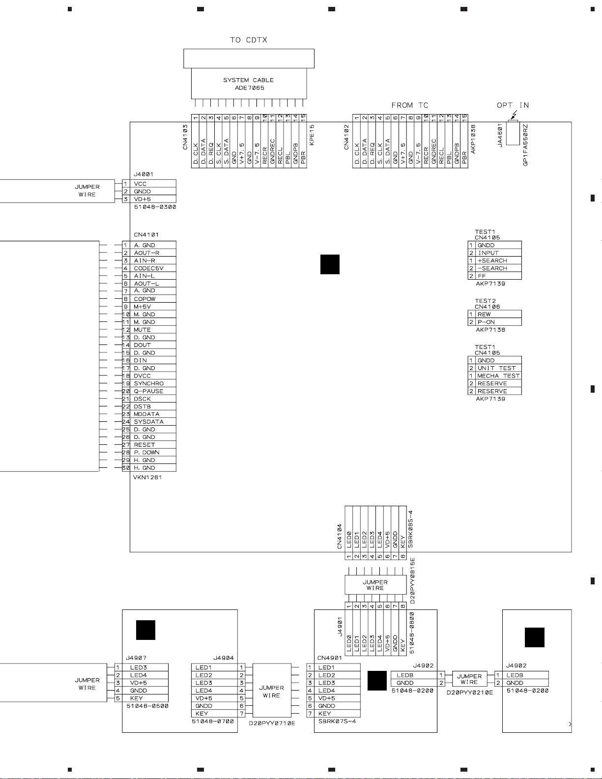
4. PCB CONNECTION DIAGRAM
NOTE FOR PCB DIAGRAMS:
1. Part numbers in PCB diagrams match those in the schematic
diagrams.
2. A comparison between the main parts of PCB and schematic
diagrams is shown below.
Symbol in PCB
Diagrams
BCE
BCE
DGS
Symbol in Schematic
Diagrams
BCE
BCEBCE
DGSDGS
BCE
Part Name
Transistor
Transistor
with resistor
Field effect
transistor
MJ-NS1
Resistor array
3-terminal
regulator
3. The parts mounted on this PCB include all necessary parts
for several destination.
For further information for respective destinations, be sure
to check with the schematic diagram.
4. Viewpoint of PCB diagrams
Capacitor
Connector
SIDE A
P.C.Board Chip Part
SIDE B
21
Page 22

1
23
MJ-NS1
4.1 MAIN , KEY-R ,KEY-L ,RELAY
BLUE and IC UNITS
4
A
B
MAIN UNIT
A
IC4001
IC4002
From
DECK
To
CD TUNER
G
CN104
(ANP7348-B)
KEY-L UNIT
D
C
KEY-R UNIT
C
D
(ANP7348-B)
(ANP7348-B)
E
BLUE UNIT
F
IC UNIT
B
RELAY UNIT
(ANP7348-B)
(ANP7348-B)
22
SIDE A
A
1234
CB
ED F
Page 23

IC4203
IC4202
1
IC4201
234
MJ-NS1
A
MAIN UNIT
A
Q4103
IC4101
IC UNIT
B
(ANP7348-B)
KEY-L UNIT
D
KEY-R UNIT
C
B
C
(ANP7348-B)
SIDE B
1
(ANP7348-B)
(ANP7348-B)
RELAY UNIT
E
D
BLUE UNIT
F
(ANP7348-B)
A
2
3
CB
(ANP7348-B)
ED F
23
4
Page 24

1
23
MJ-NS1
4.2 MD CORE MAIN and MD CORE SW UNITS
4
A
MD CORE
G
MAIN UNIT
IC108
Q102
Q101
IC104
B
IC103
IC102
IC106
C
(ANP7353-B)
MD CORE
H
IC101
SW UNIT
(ANP7353-B)
D
SIDE A
24
G
H
1234
Page 25

1
234
MJ-NS1
IC107
IC110
IC105
IC109
LOADING
MOTOR ASSY
CN4101
A
REC HEAD
MD CORE
G
MAIN UNIT
A
B
CARRIAGE
MOTOR ASSY
SPINDLE
MOTOR
(ANP7353-B)
SIDE B
MD CORE
H
SW UNIT
MD PICKUP
C
(ANP7353-B)
D
G
1
2
3
H
4
25
Page 26

MJ-NS1
Mark No. Description Part No.
Mark No. Description Part No.
5. PCB PARTS LIST
NOTES:•Parts marked by "NSP" are generally unavailable because they are not in our Master Spare Parts List.
Mark No. Description Part No.
LIST OF ASSEMBLIES
NSP MD MAIN ASSY AWM7522
NSP RELAY UNIT AWU7576
NSP KEY L UNIT AWU7577
NSP KEY R UNIT AWU7652
NSP BLUE UNIT AWU7653
NSP IC UNIT AWU7654
NSP MD CORE SW UNIT AWU7592
The mark found on some component parts indicates the importance of the safety factor of the part.
•
Therefore, when replacing, be sure to use parts of identical designation.
When ordering resistors, first convert resistance values into code form as shown in the following examples.
•
Ex.1 When there are 2 effective digits (any digit apart from 0), such as 560 ohm and 47k ohm (tolerance is shown by J=5%,
and K=10%).
560 Ω→56 × 10
47k Ω→47 × 10
0.5 Ω→R50 ..................................................................................... RN2H
1
→ 561 ........................................................ RD1/4PU 5 6 1 J
3
→ 473 ........................................................ RD1/4PU 4 7 3 J
R 5 0
1 Ω→1R0 ..................................................................................... RS1P 1 R 0 K
Ex.2 When there are 3 effective digits (such as in high precision metal film resistors).
5.62k Ω→ 562 × 10
1
→ 5621 ......................................................RN1/4PC 5 6 2 1 F
Mark No. Description Part No.
C4103,C4105,C4107,C4126 CKSQYB103K50
C4128-C4141,C4231,C4602,C4603 CKSQYB103K50
MAIN UNIT AWU7607
MD CORE UNIT AWM7516
MD CORE MAIN UNIT AWU7591
RESISTORS
C4205,C4206,C4209,C4210 CKSQYB105K10
C4217,C4218,C4239,C4240 CKSQYB105K10
C4112 CKSQYB222K50
C4604 CKSQYB332K50
C4104,C4106,C4110,C4111,C4119 CKSQYF104Z25
C4125,C4233,C4241,C4605 CKSQYF104Z25
C4003,C4004,C4010,C4127 CKSQYF105Z16
C4211,C4212,C4227,C4228 CKSQYF473Z25
All Resistors RS1/10S J
K
A
MAIN ASSY
SEMICONDUCTORS
IC4201,IC4202 BA4558F-HT
IC4008 NJM7805FA
IC4001 NJM78L05A
IC4002 NJM79L05A
IC4203 BU4066BCF
IC4101 PDG257A
IC4102 TC74HCT08AF
Q4201,Q4202 2SD2114K
Q4203,Q4204 DTA124EK
Q4102,Q4103,Q4205 DTC124EK
Q4101 DTC143EK
D4101 1SS355
D4003 S5566G(TPB2)
D4103-D4107,D4201-D4212 UDZS8.2B
COILS AND FILTERS
F4101,F4102,F4601 DTF1069
L4103,L4104 LFEA2R2J
L4110-L4112 VTL1093
CAPACITORS
C4221,C4222 CCSQCH100D50
C4115-C4118 CCSQCH221J50
C4203,C4204,C4235,C4236 CCSQSL471J50
C4005,C4006,C4108,C4223,C4224 CEAT100M50
C4229,C4230 CEAT100M50
C4001,C4002,C4011,C4016,C4109 CEAT101M10
C4601 CEAT101M10
C4201,C4202,C4219,C4220 CKSQYB102K50
C4225,C4226,C4234 CKSQYB102K50
OTHERS
3P Cable Holder 51048-0300
CN4102 15P Socket AKP1038
CN4106 Header (2P) AKP7138
CN4105,CN4107 Header (5P) AKP7139
Heat Sink ANH-575
X4101 (10.0 MHz) DSS1048
JA4601 Optical Module GP1FA550RZ
CN4103 15P Jumper Connector KPE15
PCB Binder VEF1040
CN4101 30P FFC Connector VKN1261
KN4101 Earth Plate VNF1084
B
IC UNIT
SEMICONDUCTORS
IC4006 NJM7805FA
CAPACITORS
C4009 CEAT101M10
C4008 CEAT1R0M50
OTHERS
3P Cable Holder 51048-0300
J4002 3P Parallel Cable D20PYY0310E
C
KEY-R UNIT
SEMICONDUCTORS
Q4905,Q4906 DTC124EK
D4905,D4906 LT1E40A
26
Page 27

MJ-NS1
Mark No. Description Part No.
SWITCHES AND RELAYS
S4903,S4904 ASG7013
RESISTORS
All Resistors RS1/10S J
OTHERS
5P Cable Holder 51048-0500
D
KEY-L UNIT
SEMICONDUCTORS
Q4903,Q4904 DTC124EK
D4903 LT1E40A
D4904 SML-210VT
SWITCHES AND RELAYS
S4901,S4902 ASG7013
RESISTORS
All Resistors RS1/10S J
OTHERS
5P Cable Holder 51048-0500
7P Cable Holder 51048-0700
J4907 5P Parallel Cable D20PYY0515E
J4904 7P Parallel Cable D20PYY0710E
Mark No. Description Part No.
G
MD CORE MAIN UNIT
SEMICONDUCTORS
IC110 AK4519VF
IC107 BD7910FV
IC105 BR93LC56F
IC101 IR3R55M
IC102 LR376487
IC106 M56788FP
IC103 MSM51V4400D70TSK
IC108 RN5RG32AA
IC104 PD5593A
IC109 TC74VHC08FT
Q101 2SB1188
Q102 2SC4081
D101 SBE803
D102 UDZ3.6B
COILS AND FILTERS
chip coil (4.7µH)
L101,L103,L104,L107 DTL1024
L108 chip solid inductor QTL1015
L105 chip coil (47µH) RTL1003
L102 chip coil (0.47µH) RTL1007
L116 chip beeds VTL1093
L109-L115 chip beeds VTL1105
SWITCHES AND RELAYS
S101,S102 RSF1012
E
RELAY UNIT
SEMICONDUCTORS
Q4901,Q4902 2SA1037K
CAPACITORS
C4901 CKSQYF104Z25
RESISTORS
All Resistors RS1/10S J
OTHERS
2P Cable Holder 51048-0200
8P Cable Holder 51048-0800
J4902 2P Parallel Cable D20PYY0210E
J4901 8P Parallel Cable D20PYY0815E
CN4901 Jumper Connector SBRK07S-4
PCB Binder VEF1040
F
BLUE UNIT
SEMICONDUCTORS
D4901 EB3804X
CAPACITORS
C4902 CKSQYF104Z25
OTHERS
2P Cable Holder 51048-0200
CAPACITORS
C122,C186,C215 CCSQCH101J50
C127,C128 CCSQCH120J50
C151 CCSQCH220J50
C105-C109 CCSQCH271J50
C110 CCSQCH331J50
C201,C202 CCSQCH470J50
C191,C192,C207,C209,C211 CEV100M16
C214 CEV100M16
C145,C189,C198,C213 CEV101M4
C152 CEV101M6R3
C195,C196 CEV220M6R3
C180,C182,C188 CEV470M6R3
C120 CEV4R7M35
C217 CKSQYB102K50
C139,C148,C212,C216 CKSQYB103K50
C218,C219 CKSQYB103K50
C129 CKSQYB104K25
C101,C102,C104,C117,C118 CKSQYB105K10
C166,C167 CKSQYB153K50
C193,C194 CKSQYB222K50
C137,C141,C142 CKSQYB223K50
C103,C185 CKSQYB273K50
C116 CKSQYB332K50
C115,C121 CKSQYB333K50
C112 CKSQYB472K50
C133 CKSQYB473K16
C111,C114 CKSQYB474K16
C174,C175 CKSQYB562K50
C154,C157,C162,C163 CKSQYB821K50
C135,C140,C143,C146,C155 CKSQYF104Z25
C176,C181,C183,C184,C187 CKSQYF104Z25
27
Page 28

MJ-NS1
Mark No. Description Part No.
C190,C197,C199,C204-C206 CKSQYF104Z25
C208,C210 CKSQYF104Z25
C119,C123-C126,C130,C132 CKSQYF105Z16
C134,C136,C138,C147,C164 CKSQYF105Z16
C177 CKSQYF105Z16
RESISTORS
R111 RS1/8S270J
Other Resistors RS1/10S J
OTHERS
CN104 30P Connector RKN1039
X101 (33.8MHz) RSS1055
CN105 ZR Connector S2B-ZR-SM3A
CN102 Connector 2P S2B-ZR-SM3A-R
CN106 PH Connector S5B-PH-SM3
CN101 Connector for flex. cable SFV28R-1ST
CN103 Connector for flex. cable SFW7R-2ST
H
MD CORE SW UNIT
SWITCHES AND RELAYS
S701 RSF1009
S702 RSF1010
RESISTORS
All Resistors RS1/10S J
Mark No. Description Part No.
OTHERS
CN701 Flexible Connector SFW7R-1ST
28
Page 29

6. ADJUSTMENT
6.1 MD SECTION ADJUSTMENT
Jigs and Measuring Instructions
• Thermometer
• Oscilloscope
• Optical Power Meter
• Jitter Meter
6.1.1 Necessary Adjustment Points
Exchange
PICKUP
• Test Disc
For servo system adjustment : GGF1328 (MMD-212)
For recording/playback inspection : GGF1328 (MMD-212), GGF1277 (or MMD-317)
TGYS1 (or MMD-110), Commercial discs
Adjustment pointsWhen
2 8
= Page 31–36
MJ-NS1
Exchange
Servo Base Assy (SPINDLE MOTOR)
Exchange
MD CORE MAIN UNIT
Exchange
MD HEAD
Exchange
Loading Mechanism Assy
Exchange
Servo Mechanism Assy
3 8
41 8
8
3 8
= Page 32–36
= Page 31,
33–36
= Page 36
= Page 32–36
Exchange
MD Mechanism Assy
(Loading Mechanism Assy +
Servo Mechanism Assy)
3 8
= Page 32–36
29
Page 30

MJ-NS1
6.1.2 Test Mode
Use the Remote Control Unit of Accessory or Service Remote Control Unit (GGF1067) at the Test Mode.
Note1 : It is impossible to enter the Test Mode in the Single Operation Mode.
Note2 : Unit Test Mode (U-TEST) is for inspection by the function checker of the production line.
Power on state and MD function
short the MECHA TEST pin.
[DISPLAY OF THE TESTMODE START]
No Disc Disc set
Service test mode
Press the MD 6 key.
MD mechanism test
about 1 sec.
tsm???? e??
EJECT
Correspondence key of the Test mode
Command Name
TEST MODE Short-circuit the MECHA TEST pin ESC (A85F)
EJECT 0 (MD EJECT) of the main unit key
MENU next 1
MENU next 2
MENU next 3
MENU previous
SET (Decision, Execution)
STOP
CHANGE (switch)
Set UP ¡ (SCAN) ¡ (SCAN) (A810)
Set DOWN
FORWARD
REVERSE
Remote Control Unit of
Accessory+(Main Unit Key)
MENU
¶ (REC) of the main unit key
CANCEL
DISPLAY
6 of the main unit key
7 (STOP) of the main unit key
SET SEARCH (A842)
1 (SCAN) 1 (SCAN) (A811)
+
– 4 (SKIP) (A853)
Remote Control Unit
1 (STILL) (A854)
FRM / TIM (A841)
CHAP (A840)
CHP / TIM (A813)
CLEAR (A845)
PLAY (A817)
7 / EJECT (A816)
¢ (SKIP) (A852)
CLD Service
(GGF1067)
tsm???? e??
GRT AJST
SR Code
Test Point
30
SIDE A
TEST MODE
SHORT
MAIN UNIT
Page 31

6.1.3 MD Mechanism Assy Adjustment and Check
MJ-NS1
1 Temperature Check
Note: When IC101 (RF-AMP) or IC104 (mechanical controller) has been exchanged or when a correction changing VD+3 has been made,
be sure to correctly perform all steps up to step 7.
Step No.
1
2 Press the ¶ (REC) key. TEMP??&& The microcomputer starts measuring
3
When && is 80 (not passed) TEMP??80 80 is the default value (unadjusted).
4
5 Change && with the + key and – key.
6
Operation Keys and Operation Method FL Display Status Remarks
In the Power ON state, selecting MD function,short the
"MECHA TEST pin".
When && is 80 or more at this time, the adjustment is
OK (step 4 and following can be omitted.)
Measure the ambient temperature T (°C) and check
that the measuring value (??) is within the standard in
regard to the microcomputer set value (&&).
Note: When the indication of the measuring value
(??) is not stable, and the ambient temperature T (°C)
is 25 °C or less, set to the lower value.
When the ambient temperature is over 25 °C, set to
the higher value.
Turn off the power of the CD tuner.
(Please perform this check soon after the power has been switched on.)
EJECT Test mode
??: Measuring
End
TEMP
µ-com Measuring value µ-com Set value
Room Temperature
[T (°C)]
11.6 to 16.9 Measuring value (??) –2
17.0 to 22.3 Measuring value (??) –1
22.4 to 27.6 Measuring value (??)
27.7 to 33.0 Measuring value (??) +1
33.1 to 38.4 Measuring value (??) +2
TEMP 7B 7B
hex= (?? – &&)
Data writes to the EEPROM and turns
the system power to off. Test mode
returns to the normal mode.
When the
microcomputer value
is
value
&&: Set value
79
7A
7B
7C
7D
–
+
2 Laser Power Check
Step No.
1 EJECT Test mode
2
3
4
5 Press the SET key. rpw REC power output status
6
7 Press the 7 (STOP) key. The LD goes out.
Operation Keys and Operation Method
In the Power ON state, selecting MD function,short the
"MECHA TEST pin".
Press the SET key (Remote control unit). ppw PLAY power output status
Measure the laser power with an optical power meter.
At this time, check that the measuring value (PLAY
power) meets the standard value of the table on the
right.
Note: When the standard value on the right is applied,
the numerical value immediately after entry into test
mode 2 shall be taken as the standard.
At this time, check that the measuring value (REC
power) meets the standard value of the table on the
right.
FL Display
ppw
µ-com
Measuring value
ppw May be omitted.
rpw
hex=(?? – &&)
+02 to +04 0.69 ± 0.12
–01 to +01 0.67 ± 0.1
–02 to –04 0.63 ± 0.1
hex=(?? – &&)
+02 to +04 6.18 ± 0.93
–01 to +01 5.79 ± 0.87
–02 to –04 5.47 ± 0.82
TEMP
Status
Standard value
Standard value
Remarks
Laser wavelength:
780 nm
µ-com
Set value
(mW)
(mW)
31
Page 32

MJ-NS1
3 Grating Adjustment
Press the 0 (MD EJECT) key to take out the cartridge of Optical power meter in the state of step 7 of 2 , and then it is possible from steps 2
of this item.
Step No.
1 EJECT Test mode
2 Insert the test disc GGF1328 (MMD-212).
3 Press the 6 key.
4
5 Press the 7 (STOP) key. Adjustment end
Operation Keys and Operation Method FL Display Status
In the Power ON state, selecting MD function,short the
"MECHA TEST pin".
Connect an oscilloscope according to the following
connection diagram and loosen the screw A at the
side of the adjustment hole. Turn the hole with a
screwdriver until the Lissajous waveform becomes as
shown in the figure, and then tighten the screw A.
LOADING
GRT AJST
LON :
LAg :
GEG :
GRT AJST Lissajous waveform a:b = Within 3:1
Grating adjustment state
Playback is started in tracking open state.
(The servo is closed only for focus and
spindle.)
Connection Diagram
Remarks
REFO
EOUT
Ocsilloscope
100kΩ
100kΩ
MD CORE MAIN UNIT
FOUT
470p
470p
a
b
Lissajous waveform
a:b = Within 3:1
SIDE A
Adjustment
Hole
Screw A
32
Page 33

4 Preliminary Adjustment
It is possible from steps 3 of this item in the state of step 5 of 3 .
MJ-NS1
Step No.
1 EJECT
2 Insert the test disc GGF1328 (MMD-212).
3 Press the 7 (STOP) key. Return to menu display.
4 Press the MENU key (until "AUT YOBI" is displayed). Preliminary adjustment mode
5
6
7
Note: When this adjustment is performed after defocus adjustment has been performed, defocus is returned to the initial state, and defocus
adjustment must be performed.
Operation Keys and Operation Method FL Display Status
In the Power ON state, selecting MD function,short the
"MECHA TEST pin".
Preliminary adjustment starts when the 6 key is
pressed.
Press the 7 (STOP) key.
Turn off the power of the CD tuner.
LOADING
GRT AJST
tsm????e??
AUT YOBI
HAo :
RFg :
PTG :
|
Can't ADJ.
COMPLETE
AUT YOBI Return to menu display.
Test mode
Defective adjustment
(problem with the servo system)
Adjutment end
Data writes to the EEPROM and turns the
system power to off. Test mode returns to
the normal mode.
Remarks
5 Normal Adjustment
Step No.
1 EJECT
2 Insert the test disc GGF1328 (MMD-212).
3 Press the MENU key (until "AUT YOBI" is displayed). Normal adjustment mode
4
5
Operation Keys and Operation Method FL Display Status
In the Power ON state, selecting MD function,short the
"MECHA TEST pin".
Normal adjustment starts when the 6 key is
pressed.
Press the 7 (STOP) key.
LOADING
GRT AJST
AUT AJST
PEG :
HAG :
|
Can't ADJ.
COMPLETE
AUTO AJST Return to menu display.
Test mode
Defective adjustment
(problem with the servo system)
Adjutment end
Remarks
33
Page 34

MJ-NS1
6 Defocus Adjustment
It is possible from steps 3 of this item in the state of step 5 of 5 .
Step No.
1 EJECT
2
3 Press the MENU key.(until "deFO AJST" is displayed.) deFO AJST
4
5
6 Press the ¶ (REC) key.
7
8
9
10 Press the 6 key. COMPLETE
11 Turn off the power of the CD tuner. Release from the test mode.
Operation Keys and Operation Method FL Display Status
In the Power ON state, selecting MD function,short the
"MECHA TEST pin".
Insert the test disc GGF1328 (MMD-212).
Press the 6 key.
of c
Defocus Value C1 Error Value
Check the jitter value and end the adjustment when
the intermediate jitter value is 29 nsec or less.
Press the ¶ (REC) key. of-04 c0020
When J+ is larger than J-, press the ¶ (REC) key and
display the C1 error when the focus offset is applied
up to +0.4µm.
(Do nothig when J- is larger than J+.)
Change the value with 1 and ¡ keys until the
value becomes the same.
LOADING
GRT AJST
PEG :
FESpp :
of000c0015
of+04 c0032
of+04 c0032
of+04 c0032
of+03 c0025
of+02 c0020
Test mode
Defocus mode is entered, and after
automatic execution of normal adjustment,
the C1 error at the time of focus offset 0 is
displayed.
The C1 error with application of a focus
offset of about 0.4µm on the + side is
displayed. The jitter value (J+) at this time
is recorded.
The C1 error with application of a focus
offset of about 0.4µm on the – side is
displayed. The jitter value (J–) at this time
is recorded.
When the smaller offset of the jitter value
has been corrected mistakenly, press the
ENTER key and return to step 4.
The mean value of the changed set value
and the offset of the other setting limit is
written into the EEPROM as the
compensation offset.
Remarks
Connection Diagram
Jitter Meter
LEVEL
GND
MD CORE MAIN UNIT
SIDE A
JITTER
EFM MON
REFO
34
Page 35

7 Jitter/C1 Error Check at the time of Playback
Step No.
1
2
3
4
5
6
7
8
9
10
11
12
13
14
15
Operation Keys and Operation Method
In the Power ON state, selecting MD function,short the
"MECHA TEST pin".
Insert the test disc GGF1328 (MMD-212).
Perform "5 Normal Adjustment" (steps 3 to 5).
Press the ¶ (REC) key.
Press the SET key and display the inner
circumference address.
Press the 6 key and display the C1 error for the
inner circumference.
Press the DISPLAY key.
Press the DISPLAY key.
Press the 7 (STOP) key.
Press the SET key and display the inner
circumference address.
Press the ¶ (REC) key and display the intermediate
circumference address. Perform steps 6 to 9 in this
condition.
Press the SET key and display the inner
circumference address.
Press the ¶ (REC) key twice to display the outer
circumference address. Perform steps 6 to 9 in this
condition.
Press the 0 (MD EJECT) key, eject the test disc
GGF1328 (MMD-212), and insert TGYS1 (or MMD-
110).
Perform steps 3 to 13 and check the jitter/C1 error with
the test disc TGYS1 (or MMD-110).
FL Display
LOADING
GRT AJST
AUT AJST
TEST PLAY TEST PLAY mode
ADRES 0050
a0050 c0015
A0062 c0013
AVE. c0012
a006F c0017
TEST PLAY
ADRES 0050
ADRES 03C0
a03C0 c0009
TEST PLAY
ADRES 0050
ADRES 0700
a0700 c0008
TEST PLAY
LOADING
GRT AJST
a0062 c0009
a03d2 c0007
a0712 c0006
EJECT
EJECT
MJ-NS1
Status
Test mode
Check that the jitter value meets the
standard value of the following table.
GGF1328 (MMD-212) jitter value
Inner circumference 31 nsec or less
Intermediate circumference 29 nsec or less
Outer circumference 29 nsec or less
Seven data are acquired, the largest and
the smallest value are discarded, and fixed
display is made for the mean value of the
remaining five data. Check that this value
is 200 or less.
The fixed display of the C1 error is enabled.
Check that the jitter value meets the
standard value of the following table.
TGYS1 (or MMD-110) jitter value
Inner circumference 29 nsec or less
Intermediate circumference 27 nsec or less
Outer circumference 27 nsec or less
Remarks
Intermediate and outer
circumference may be omitted.
Press the 0 (MD EJECT) key.
16
Power OFF Release from the test mode.
17
Connection Diagram
Jitter Meter
LEVEL
GND
JITTER
REFO
EJECT
MD CORE MAIN UNIT
EFM MON
The test disc TGYS1 (or MMD-110) is ejected.
SIDE A
35
Page 36

MJ-NS1
8 Jitter/C1 Error Check at the time of Recording/Playback
Step No.
1 EJECT
2
3 AUTO AJST
4 TEST REC
5
6
7
8
9 Perform step 6.
10
11
12 Perform step 6.
13
14
Operation Keys and Operation Method
In the Power ON state, selecting MD function,short the
"MECHA TEST pin".
Insert the test disc GGF1277 (or MMD-317).
Perform "5 Normal Adjustment" (steps 3 to 5).
Press the ¶ (REC) key.
Press the SET key and display the inner
circumference address.
When the 6 key is pressed, TEST REC starts, and
when 25 addresses or more have been sent, stop by
pressing the 7 (STOP) key.
Press the SET key and display the inner
circumference address.
Press the ¶ (REC) key and display the intermediate
circumference.
Press the SET key and display the inner
circumference address.
Press the ¶ (REC) key twice and display the outer
circumference address.
Press the ¶ (REC) key.
Perform steps 5 to 13 of " 7 Jitter/C1 Error Check at
the time of Playback".
At the time of self-recording, wait for seven addresses
after TEST PLAY start, and then press the DISPLAY
key and enter into mean value mode.
(Good recording may not be possible for several
addresses at the beginning.)
FL Display
Test mode
LOADING
GRT AJST
TEST REC mode
a0050 pw0D
a0069 pw0D
TEST REC
a0050 pw0D
a03C0 pw0D
a03D9 pw0D
TEST REC
a0050 pw0D
a0700 pw0D
a0719 pw0D
TEST REC
TEST PLAY TEST PLAY mode
a0069 c0009
a03D9 c0007
a0719 c0006
Note:
When the initial address (0050) part of the
inner circumference (or intermediate/outer
circumference) has been used 1000 times
or more, press the 2 (SCAN) key and shift
the address by 10 hex. (The address is
shifted (up to 10 times) according to the
use frequency of the disc.)
Check that the jitter/C1 error at the
inner/intermediate/outer circumference of
GGF1277, and check that the jitter value
satisfies the standard value of the
following table.
GGF1277 jitter value
Status
Inner circumference 33 nsec or less
Intermediate circumference 31 nsec or less
Outer circumference 31 nsec or less
Remarks
Intermediate and outer
circumference may be omitted.
Press the 0 (MD EJECT) key.
15
Turn off the power of the CD tuner. Release from the test mode.
16
Connection Diagram
Jitter Meter
LEVEL
GND
JITTER
REFO
EJECT
MD CORE MAIN UNIT
EFM MON
The test disc (GGF1277) is ejected.
SIDE A
36
Page 37

7. GENERAL INFORMATION
SIDE B
MAIN UNIT
DC +9V
POWER SUPPLY POINT
DC –9V
GND
7.1 DIAGNOSIS
7.1.1 SINGLE OPERATION MODE
How to enter the single operation mode
1. Supply DC power to CN4103 power supply pin of the MD MAIN
UNIT. (Pin7 : +9V ,Pin8 : GND ,Pin9 : –9V)
2. Short-circuit the "P-ON" pin and "GND" pin.
Key operation in the single operation mode
[REC] : To record
[PLAY] : To playback
[STOP] : To stop the recording and playing
[EJECT] : To eject
[INPUT] (IN) : To switch the input in the recording mode
(Digital/Analog)
[+] : To search track forward
[–] : To search track reverse
[CUE] (FF) : To forward
[REV] : To reverse
MD key
MJ-NS1
About the recording input switch
Recording input is able to switch with the "INPUT" key.
Digital and analog are selected alternately whenever press the
"INPUT" key. Initial value is the Digital input mode.
Note:
(1) Recording input can switch only during REC PAUSE.
(2) Blue LED of the center of MD flashes in the single operation
mode.
(3) It cannot enter the adjustment mode of the mechanism unit in
the single operation mode.
Test Point
Short-circuit
MAIN UNIT
SIDE A
37
Page 38

MJ-NS1
7.1.2 POWER ON SEQUENCE
Outline
• When MD mechanism is normal, an operation of MD is decided whether communication is done normally.
When MD mechanism does not perform a correct operation, first confirm waveform of communication. (Refere to step 1.)
• The command that System controller transfers please refer to 4 from step 2.
1. Reset and communication
When it becomes the state that a mechanism controller can communicate,
Mech.
power
supply
PDOWN
RESET
DSTB
turn DSTB into "L".
DSCK
SYSDATA
MDDATA
System controller confirms that
DSTB became "L", and output
a clock. System controller and
Mechanism controller output
data in accordance with it.
2. Power ON
User
System controller
Mech.
controller
(MD mech.)
RESET
System controller always grasps the state of MD mechanism.
1 byte
32 byte
1 communication
Power on
Power on
command issue
INIT STANDBY EJECT END (NO DISC state)
Mechanism controller turns
DSTB into "H" if received
32 bytes.
38
Page 39

3. Disc insertion and TOC READ
MJ-NS1
User
System controller
Mech.
controller
(MD mech.)
4. PLAY
User
Insert a disc
TOC READ
command issue
EJECT END (NO DISC state)
• System controller always grasps the state of MD mechanism.
• Mechanism controller (MD mechanism) detects it when inserts a disc, and start loading.
• When do not perform a disc loading, it cannot conclude with defectiveness of MD Mechanism immediately.
Because when communication between System controller and mecanism controller does not complete,
do not perform a disc loading either.
Press the MD PLAY key
LOAD STOP STOPTOC READ
System controller
Mech.
controller
(MD mech.)
PLAY
command issue
STOP
• System controller always grasps the state of MD mechanism.
SEARCH PLAY
39
Page 40

MJ-NS1
7.1.3 DISASSEMBLY
Top Panel and MD Mechanism
Rear side
MD
Mechanism
1
1
17
KEY-R UNIT
KEY-L UNIT
IND UNIT
16
Top Panel MD
IC UNIT
3
× 3
MAIN UNIT
RELAY UNIT
12
14
Go to MD Mechanism Assy
MD Mechanism Assy
MD Shield Case
5
× 4
• Removal of the MD Mechanism Assy
1 Remove a screw A.
2 Disconnect the connectors (CN102, CN103 and CN105), open
the hook of part A, and tilt the upper side of the MD CORE
MAIN UNIT to the front.
3 Disconnect the connector (CN101) at the rear of the MD
CORE MAIN UNIT and remove the MD CORE MAIN UNIT.
2
CN105
Screw A
1
CN102
2
MD CORE MAIN UNIT
CN101
CN103
2
Part A
3
40
Page 41

MJ-NS1
4 Shift part B to the position shown in the figure while raising the
Under Slider. (At the same time, the Upper Slider moves to the
front.)
5 Remove the Lock Plate. (One screw C)
4
Part B
Under Slider
Upper Slider
• Removal of the MD Pickup
1 Remove the MD Head. (One screw A)
2 Remove the Screw Guide at the lower side of the MD Pickup.
(One screw B)
3 Remove the S. H. Spring. (One screw C)
4 Remove the hook of the S. H. Spring as shown in the figure.
Remove the hook after the
4
screw has been removed.
1
Screw A (M1.7 × 4)
MD Head
Screw C
3
(M1.7 × 3)
S. H. Spring
Servo Mechanism
Assy
Screw C
Lock Plate
5
6 Remove the Servo Mechanism Assy.
Servo Mechanism
Assy
6
• Caution for the time of installation of the servo
mechanism assy
Move the MD Pickup to the innermost circumference.
The Servo Mechanism Assy is not installed other than the
innermost circumference.
Screw Guide
2
5 Raise the left side of the Guide Shaft and pull it out to the left.
6 Remove the MD Pickup. (With the front facing down, remove it
to the front. At this time, the MD Pickup can be removed more
easily when the Reference Plate is removed.)
Guide
5
Shaft
Hook
Reference Plate
Screw B
(M1.4 × 2)
6
MD Pickup
41
Page 42

MJ-NS1
• MD Pickup Installation
Perform installation in reverse order of the removal. (Please use
care as the MD Head mounting screw can be crushed easily.
MD Head mounting screw tightening torque: 1.1 kg • cm
When the Reference Plate has been removed, confirm that the
hook is engaged with the shaft of the spindle motor. (Take care
that the mounting reference boss does not ride up.)
• S. H. Spring Installation
S. H. Spring
1
Insert
• Removal of the Head Lifter
1 Remove the Lifter SP.
2 Tilt the Head Lifter to the rear and push part A to disengage it.
Head Lifter
1
Lifter SP
Push
2
Part A
• Head Lifter Installation
1 Install part A in the Servo Base with the Head Lifter tilted to the
back.
2 Match the Head Lifter and the Servo Base as shown in the
figure, and then engage part B.
3 While holding part B with your hand, tilt the Head Lifter to the
front and install the Lifter SP.
2
Push in while changing
the point.
3
Press in with a screwdriver
or similar until the hook
becomes engaged.
Head Lifter
Head Lifter
Servo Base
Push
Part B
Part B
3
2
Part A
Matching
position
1
42
Confirm from the rear that the tip of
the hook is engaged sufficiently.
Page 43

MJ-NS1
7.2 IC
• The information shown in the list is basic information and may not correspond exactly to that shown in the schematic diagrams.
PDG257A [MAIN UNIT (2/2) : IC4101]
• System Control U-COM
No.
1
2
3
4
5
6
7
8
9
10
11
12
13
14
15
16
17
18
19
20
21
22
23
24
25
26
27
28
29
30
31
32
33
34
35
36
37
38
39
40
41
42
43
44
45
46
47
48
49
50
FUCTION
PF3
PF4
PF5
PF6
PF7
PD0
PD1
PD2
PD3
PD4
PD5
PD6
PD7
PC0
PC1
PC2
PC3
PC4
PC5
PC6
PC7
PH0
PH1
PH2
PH3
PH4
PH5
PH6
PH7
RST
EXTAL
XTAL
Vss
PE6
PE7
Avss
Avref
PA0/AN0
PA1/AN1
PA2/AN2
PA3/AN3
PA4/AN4
PA5/AN5
PA6/AN5
PA7/AN7
PB0/LAT0
PB1/CS0
PB3/SCK0
PB3/SI0
PB4/SC0
PIN NAME NOTE ACTIVE
D.MUTE
(NC)
(NC)
(NC)
(NC)
TEST
TESTU
CHARA
(NC)
COPOW
(NC)
(NC)
(NC)
(NC)
LED1
LED2
LED3
LED4
DIM(MID)
DIM(HIGH)
(NC)
M.RST
M.MUTE
DSTB
P.DOWN
(NC)
XPBMUTE
(NC)
OUTSEL
RESET
EXTAL
XTAL
VSS
(NC)
(NC)
AVSS
AVREF
KEY0
KEY1
(NC)
(NC)
S.DATA
S.DATAIN
(NC)
PROTECT
(NC)
(NC)
DSCK
MD DATA
SYS DATA
I/O
DIN MUTE H: MUTE
O
O
O
O
O
MECHA TEST MODE Input
I
UNIT TEST MODE Input
I
CHARACTER Exist or Not (types) input L : Chara. exist
I
O
Codec Power control
O
O
O
O
big current port (12mA)
O
MONO LP big current port (12mA)
O
REC big current port (12mA)
O
DIGITAL big current port (12mA)
O
PLAY big current port (12mA)
O
H : light L : dark
O
H : H : L :
O
big current port (12mA)
O
MD MECHANISM control Rest Input
O
MD MECHANISM control MUTE request Input
I
MD MECHANISM control communication request Input
I
MD MECHANISM control power down detection output
O
O
MDPBMUTE output
O
O
PBSELECT output L : MD H: other
O
RESET
I
input terminal for ceramic oscillator device (10MHz)
I
output terminal for ceramic oscillator device
O
O
O
O
O
key detection input 0
I
key detection input 1
I
O
O
system bus data output
O
system bus data input
I
O
abnornal voltage detection input normal : 2.5V
I
O
O
MD MECHANISM control communication clock output
O
MD MECHANISM control communication data input
I
MD MECHANISM control communication data output
O
H
L
L
H
H
H
H
H
L
L
L
L
-
-
-
-
-
-
-
-
-
-
-
-
-
-
-
-
43
Page 44

MJ-NS1
No.
51
52
53
54
55
56
57
58
59
60
61
62
63
64
65
66
67
68
69
70
71
72
73
74
75
76
77
78
79
80
• I/O port is able to select function as input or output by 1bit unit.
FUCTION
PB5/SCK1PF4
PB6/SI1
PB7/SO1
PE0/EC0
PE1/EC1
PE2/CINT
PE3/NM1
PE4/PWM0
PES/TO/PWM1
PI0/INT0
PI1/INT1
PI2/INT2
PI3/INT3
PI4
PI5
PI6
PI7
PG0
PG1
PG2
PG3
VDD
NC
PG4
PG6
PG6
PG7
PF0
PF1
PF2
PIN NAME NOTE ACTIVE
D.CLK
(NC)
D.DATA
(to GND)
(to GND)
(to GND)
(to GND)
(NC)
(NC)
S.CLK
D.REQ
(NC)
(NC)
(NC)
(NC)
(NC)
(NC)
(NC)
(NC)
(NC)
(NC)
VDD
(NC)
DSTB
(NC)
(NC)
(NC)
(NC)
(NC)
(NC)
I/O
I/O
I/O
I
I
I
I
I
O
O
I
I
-
O
O
O
O
O
O
O
O
O
O
O
O
O
O
O
O
MD display communication clock output
MD display communication data output
Take care to use also device test terminal
Take care to use also device test terminal
system bus clock input
MD display communication request input
-
44
Page 45

AK4519VF [MD CORE MAIN UNIT : IC110]
• Audio Codec IC
MJ-NS1
.
.
.
45
Page 46

MJ-NS1
8. PANEL FACILITIES AND SPECIFICATIONS
4
3
5
2
6
1
7
8
9
Top Panel
1. 6 – Press to play an MD, or pause one that's already
playing (press again to restart playback). In record mode,
also use to start or pause recording.
2. 7 – Press to stop playback or recording of the current MD.
3. MD loading slot
4. ¶ – Press to record.
5. 0 – Press to eject the MD.
46
Front Panel
6. MD REC indicator – Lights up during record or record-pause
mode.
7. Mono indicator – Lights up when recording in mono.
8. PLay indicator – Lights up while paused or during playback.
9. Digital indicator – Lights up when MD recorder is in digital
signal input mode.
Page 47

SPECIFICATIONS
Recording method Magnetic field modulation
overwritten type
Playback method ........Non-contact optical type
Sampling frequency 44.1KHz,32KHz,48KHz
Frequency response................... 20Hz – 20KHz
Wow and flutter............... Limit of measurement
(±0.001% W.PEAK) or less (EIAJ)
Power requirements ...................................... DC
Dimensions ........ 170(W) × 268(H) × 66 (D) mm
(without stands)
Weight ........................................................ 1.5kg
Accessories
Optical digital cable .......................................... 1
Stand A.............................................................. 1
Stand B............................................................. 1
Operating instructions ...................................... 1
Note: Specifications and design subject to possible
modification without notice,due to improvement.
MJ-NS1
Cleaning external surfaces
To clean this unit,wipe with a soft,dry cloth. For
stubborn dirt,wet a soft cloth with mild detergent
solution made by diluting one part detergent to 5
or 6 parts water,wring well,then wipe off the dirt.
Use a dry cloth to wipe the surface dry. Do not
use volatile liquids such as benzene and thinner
which may damage the surfaces.
Accessories
Optical digital cable
(RKX1031)
Stand A
(AXG7096)
Stand B
(AXG7097)
47
 Loading...