

Page 1
MINIDISC RECORDER
MINIDISC RECORDER
MJ-D707
TIMER
REC
OFF
PLAY
DISC LOADING MECHANISM
PUSH ENTER
EDIT
/
NO
NAME
ANALOG
COAX
OPT
0
1
2
3
4
5
6
7
8
9
10
INPUT SELECTOR REC LEVEL
DIGITAL
NR
REPEAT
A B
TIME SKIP
PLAY
MODE
REC
MODE
NAME
CLIP
DISPLAY
/ CHARA
STANDBY
POWER
— OFF _ ON
SYNCHRO
REC
MIN
MAX
PHONES
LEVEL
)
EJECT
$
$
!
!
#
*
&
Î
Legato Link Conversion
MJ-D707
MJ-17D
THIS MANUAL IS APPLICABLE TO THE FOLLOWING MODEL(S) AND TYPE(S).
ORDER NO.
RRV1963
Type
Model
MJ-D707 MJ-17D
KU AC120V
MY –– AC220–230V
MY/GR/FR –– AC220–230V
CONTENTS
1. SAFETY INFORMATION....................................2
2. EXPLODED VIEWS AND PARTS LIST .............4
3. SCHEMATIC DIAGRAM...................................12
4. PCB CONNECTION DIAGRAM ....................... 28
5. PCB PARTS LIST.............................................37
6. ADJUSTMENT..................................................41
Power Requirement
Remarks
7. GENERAL INFORMATION .............................. 49
7.1 PARTS .......................................................49
7.1.1 IC .......................................................49
7.1.2 DISPLAY ...........................................60
7.2 DIAGNOSIS................................................61
7.2.1 DISASSEMBLY .................................61
7.2.2 DETAILS OF ERROR DISPLAY .......63
7.3 BLOCK DIAGRAM......................................65
8. PANEL FACILITIES AND SPECIFICATIONS
.......................................................66
PIONEER ELECTRONIC CORPORATION 4-1, Meguro 1-Chome, Meguro-ku, Tokyo 153-8654, Japan
PIONEER ELECTRONICS SERVICE, INC. P.O. Box 1760, Long Beach, CA 90801-1760, U.S.A.
PIONEER ELECTRONIC (EUROPE) N.V . Haven 1087, Keetberglaan 1, 9120 Melsele, Belgium
PIONEER ELECTRONICS ASIACENTRE PTE. LTD. 501 Orchard Road, #10-00 Wheelock Place, Singapore 238880
PIONEER ELECTRONIC CORPORATION 1998
T–DZE JUNE 1998 Printed in Japan
Page 2
MJ-D707, MJ-17D
1. SAFETY INFORMATION
This service manual is intended for qualified service technicians; it is not meant for the casual
do-it-yourselfer. Qualified technicians have the necessary test equipment and tools, and have been
trained to properly and safely repair complex products such as those covered by this manual.
Improperly performed repairs can adversely affect the safety and reliability of the product and may
void the warranty. If you are not qualified to perform the repair of this product properly and safely, you
should not risk trying to do so and refer the repair to a qualified service technician.
WARNING
This product contains lead in solder and certain electrical parts contain chemicals which are known to the state of California to
cause cancer, birth defects or other reproductive harm.
Health & Safety Code Section 25249.6 – Proposition 65
NOTICE
(FOR CANADIAN MODEL ONLY)
Fuse symbols (fast operating fuse) and/or (slow operating fuse) on PCB indicate that replacement parts
must be of identical designation.
REMARQUE
(POUR MODÈLE CANADIEN SEULEMENT)
Les symboles de fusible (fusible de type rapide) et/ou (fusible de type lent) sur CCI indiquent que les
pièces de remplacement doivent avoir la même désignation.
(FOR USA MODEL ONLY)
1. SAFETY PRECAUTIONS
The following check should be performed for the
continued protection of the customer and service
technician.
LEAKAGE CURRENT CHECK
Measure leakage current to a known earth ground
(water pipe, conduit, etc.) by connecting a leakage
current tester such as Simpson Model 229-2 or
equivalent between the earth ground and all exposed
metal parts of the appliance (input/output terminals,
screwheads, metal overlays, control shaft, etc.). Plug
the AC line cord of the appliance directly into a 120V
AC 60 Hz outlet and turn the AC power switch on. Any
current measured must not exceed 0.5 mA.
Reading should
not be above
0.5 mA
Earth ground
Device
under
test
Also test with plug
reversed
(Using AC adapter
plug as required)
Leakage
current
tester
Test all exposed
metal surfaces
AC Leakage Test
ANY MEASUREMENTS NOT WITHIN THE LIMITS
OUTLINED ABOVE ARE INDICATIVE OF A POTENTIAL SHOCK HAZARD AND MUST BE CORRECTED BEFORE RETURNING THE APPLIANCE
TO THE CUSTOMER.
2. PRODUCT SAFETY NOTICE
Many electrical and mechanical parts in the appliance have special safety related characteristics. These
are often not evident from visual inspection nor the
protection afforded by them necessarily can be obtained by using replacement components rated for
voltage, wattage , etc. Replacement parts which have
these special safety characteristics are identified in
this Service Manual.
Electrical components having such features are
identified by marking with a
on the parts list in this Service Manual.
The use of a substitute replacement component which
does not have the same safety characteristics as the
PIONEER recommended replacement one, shown in
the parts list in this Service Manual, may create shock,
fire, or other hazards.
Product Safety is continuously under review and
new instructions are issued from time to time. For
the latest information, always consult the current
PIONEER Service Manual. A subscription to, or additional copies of, PIONEER Service Manual may be
obtained at a nominal charge from PIONEER.
on the schematics and
2
Page 3
MJ-D707, MJ-17D
THIS PIONEER APPARATUS CONTAINS
LASER OF CLASS 1.
SERVICING OPERATION OF THE APPARATUS
SHOULD BE DONE BY A SPECIALLY
INSTRUTED PERSON.
LABEL CHECK
IMPORTANT
MY and MY/GR/FR types
LASER DIODE CHARACTERISTICS
MAXIMUM OUTPUT POWER: 32 mw
WAVELENGTH: 785 nm
Additional Laser Caution
Laser pick-up assembly
The output power at the objective lens of this assembly is 0.73 mW.
Control method of the current through a laser diode.
The resistor R105 on the CORD MAIN UNIT ASSY (For MD
mechanism assembly) are for the limiting of current through a laser
diode.
Control method of the laser output power
The laser pick-up assembly provide the photo-diodes and APC
(Auto Power Control) circuit.
The photo-diode detect output of the laser diode then IC104 control
the APC circuit according to the signal voltage of the photo-diode via
IC101.
The Variable resistancer on the FPC in the Laser pick-up assembly
can be adjusted the output level of Laser diode to fix the rated output
level.
Laser Interlock Switch
The loading position detect switch S101 is set to “ LOAD ON ” (ON:
low level, OFF: high level) position, IC104 get the “ LOAD ” signal,
and hand the laser “ LDON ” signal to No. 9 terminal (LDON) of the
Laser pick-up assembly.
Then a laser diode can be lighted exept when the level of signal
“LOAD ” is low.
∗ Refer to page 42.
3
Page 4
MJ-D707, MJ-17D
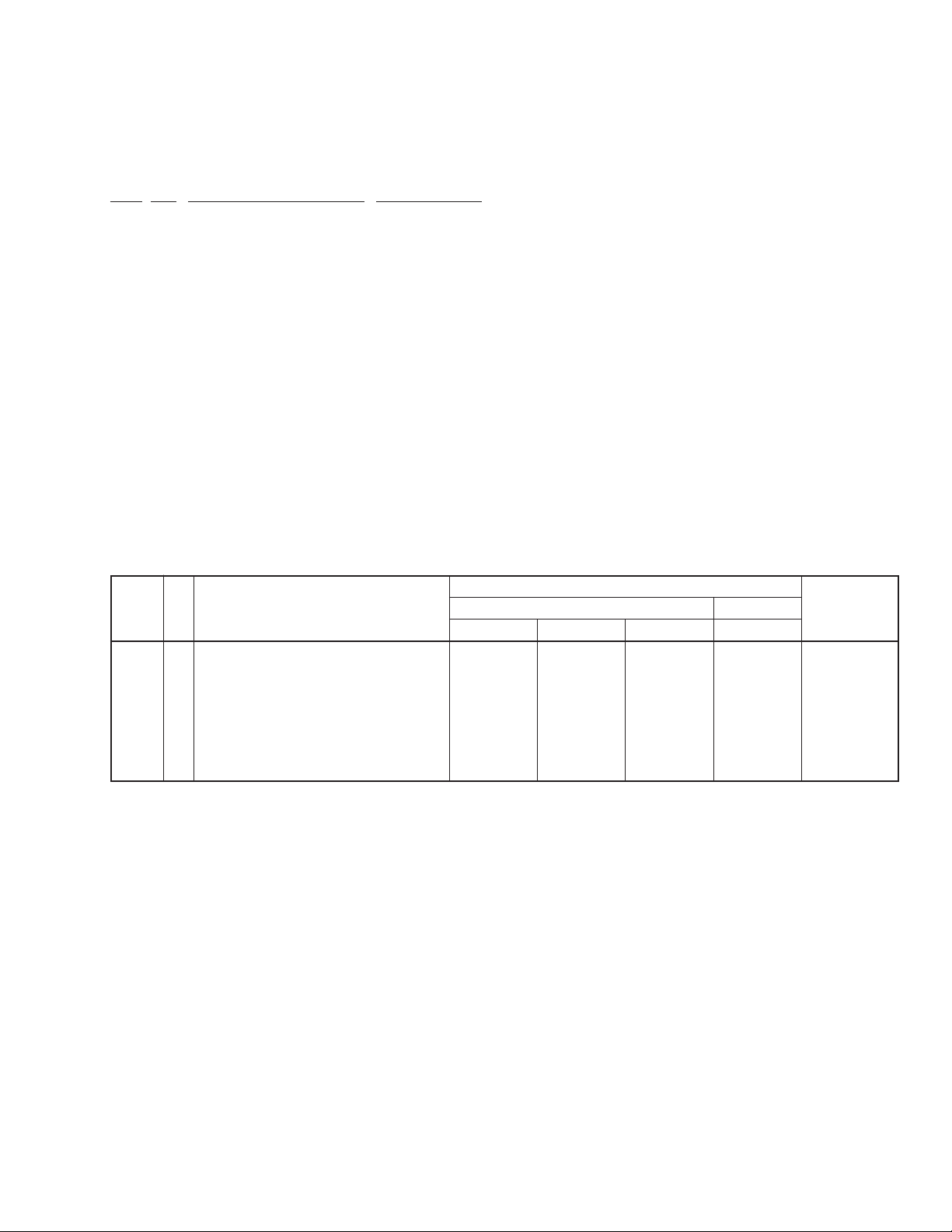
2. EXPLODED VIEWS AND PARTS LIST
NOTES : Parts marked by “ NSP ” are generally unavailable because they are not in our Master Spare Parts List.
The mark found on some component parts indicates the importance of the safety factor of the part.
Therefore, when replacing, be sure to use parts of identical designation.
Screw adjacent to mark on the product are used for disassembly.
2.1 PACKING
2 (1/2)
2 (2/2)
6
RANDOMHI-LITE MEDLEY FADER
STANDBY/ ON
REPEAT PGM CHECK CLEAR
1 2 3
ABC DEF
GHI JKL MNO
4 5 6
PQRS TUV WXYZ
7 8 9
DISP
CHARA
/
MARK
EDIT
10/0
/
NO
REC
SYNCHRO
NAME
>
!
10
REC
CURSOR
NAME
CLIP
&
!
ENTERA B
$
*
MINIDISC
REMOTE CONTROL UNIT
#
RECORDER
$
TIME
SKIP
Î
9
7
8
10
11 (MJ-D707/KU, MY only)
12 (MJ-D707/MY, MY/GR/FR only)
13 (MJ-D707/MY only)
14 (MJ-17D/KU only)
5
4
1 (2/2)
1 (1/2)
3
4
Page 5
(1) PACKING PARTS LIST
Mark No. Description Part No.
1 Protector (F) RHA1238
2 Protector (R) RHA1239
3 Packing Case
4 Sheet (750 × 600 × 0.5) Z23–007
5 Audio Cord (L= 1m) PDE1248
6 Remote Control Unit RPX1131
(CU-MJ011)
7 Battery Cover RZN1156
NSP 8 Batteries (AA/R6P) VEM–013
9 Polyethylene Bag Z21–038
(0.03 × 230 × 340)
NSP 10 Warranty Card
See Contrast table (2)
See Contrast table (2)
MJ-D707, MJ-17D
11 Operating Instructions
12 Operating Instructions
13 Operating Instructions
14 Operating Instructions
See Contrast table (2)
See Contrast table (2)
See Contrast table (2)
See Contrast table (2)
(2) CONTRAST TABLE
MJ-D707/KU, MY, MY/GR/FR and MJ-17D/KU are constructed the same except for the following:
Part No.
Mark
No.
3 Packing Case RHG1876 RHG1874 RHG1874 RHG1877
NSP 10 Warranty Card ARY1044 ARY7008 ARY7008 ARY1026
11 Operating Instructions (English/Spanish) RRE1162 RRE1162 Not used Not used
12 Operating Instructions (French/German) Not used RRD1198 RRD1198 Not used
13 Operating Instructions Not used RRD1199 Not used Not used
14 Operating Instructions (English) Not used Not used Not used RRB1185
Symbol and Description
(Portuguese/Italian/Dutch/Swedish)
MJ-D707 MJ-17D
KU MY MY/GR/FR KU
Remarks
5
Page 6
MJ-D707, MJ-17D
20 (Except MJ-17D/KU)
2.2 EXTERIOR
4
21
20 (Except MJ-17D/KU)
MJ-17D/KU only
28
25
24
21
21
MJ-17D/KU only
17
21
21
9
5
Refer to “2.4 MD
MECHANISM ASSY”.
29
31
30
25
24
21
14
35
9
16
3
21
11
23
MY and MY/GR/FR
types only
23
13
21
7
18
21
C
CN602
33
10
21
10
33
12
21
22
D
C
36
21
B
A
21
27
32
D
CN601
B
A
21
6
34
37
2
8
CN401
15
19
26
CN402
22
36
CN403
1
18
Refer to “2.3 FRONT PANEL SECTION”.
21
6
Page 7
(1) EXTERIOR PARTS LIST
MJ-D707, MJ-17D
Mark No. Description Part No.
1 MAIN UNIT ASSY
2 TRANS UNIT ASSY
3 Strain Relief
4 AC Power Cord
5 Lead Card 30P RDD1402
6 Fuse
7 Power Transformer RTT1316
NSP 8 PCB Holder PNW2100
9 Float Screw RBA1133
10 Float Rubber REB1328
11 Rear Panel
12 Mecha Angle RNB1133
13 Under Base RNB1134
14 Shield Case RNB1139
NSP 15 PC Support VEC1549
NSP 16 MD Mechanism Assy RXA1773
17 Bonnet PYY1147
18 Insulator PNW2766
19 POWER Button B RAC2207
20 Screw
See Contrast table (2)
See Contrast table (2)
See Contrast table (2)
See Contrast table (2)
See Contrast table (2)
See Contrast table (2)
See Contrast table (2)
Mark No. Description Part No.
21 Screw IBZ30P060FCC
22 Screw IBZ30P080FCC
23 Binder ZCA–SKB90BK
24 Screw
25 Wood Collar
26 Gold Mole (L)
27 Gold Mole (R)
28 Side Wood (L)
29 Side Wood (R)
30 Caution Label
31 Caution Label
32 Screw BBT30P080FCC
33 Screw RBA1132
34 Fuse Label
35 Case Spacer REB1330
36 Plate VNE1164
37 Fuse Caution Label
(2) CONTRAST TABLE
MJ-D707/KU, MY, MY/GR/FR and MJ-17D/KU are constructed the same except for the following:
See Contrast table (2)
See Contrast table (2)
See Contrast table (2)
See Contrast table (2)
See Contrast table (2)
See Contrast table (2)
See Contrast table (2)
See Contrast table (2)
See Contrast table (2)
See Contrast table (2)
Mark
Part No.
No.
Symbol and Description
MJ-D707 MJ-17D
KU MY MY/GR/FR KU
1 MAIN UNIT ASSY RWZ4309 RWZ4293 RWZ4293 RWZ4288
2 TRANS UNIT ASSY RWZ4313 RWZ4297 RWZ4297 RWZ4292
3 Strain Relief CM–22C CM–22B CM–22B CM–22C
4 AC Power Cord PDG1015 PDG1003 PDG1003 PDG1015
6 Fuse (1A/125V) REK1075 Not used Not used REK1075
6 Fuse (500mAL250V) Not used REK1019 REK1019 Not used
11 Rear Panel RNA2204 RNA2204 RNA2204 RNA2205
20 Screw
24 Screw Not used Not used Not used PBA1103
25 Wood Collar Not used Not used Not used PNW1238
26 Gold Mole (L) Not used Not used Not used RAH2865
27 Gold Mole (R) Not used Not used Not used RAH2866
28 Side Wood (L) Not used Not used Not used RMS1019
29 Side Wood (R) Not used Not used Not used RMS1020
30 Caution Label Not used RRW1233 RRW1233 Not used
31 Caution Label Not used VRW1094 VRW1094 Not used
34 Fuse Label RRW1294 Not used Not used RRW1294
37 Fuse Caution Label RRW–111 Not used Not used RRW–111
FBT40P080FZK FBT40P080FZK FBT40P080FZK
Not used
Remarks
7
Page 8
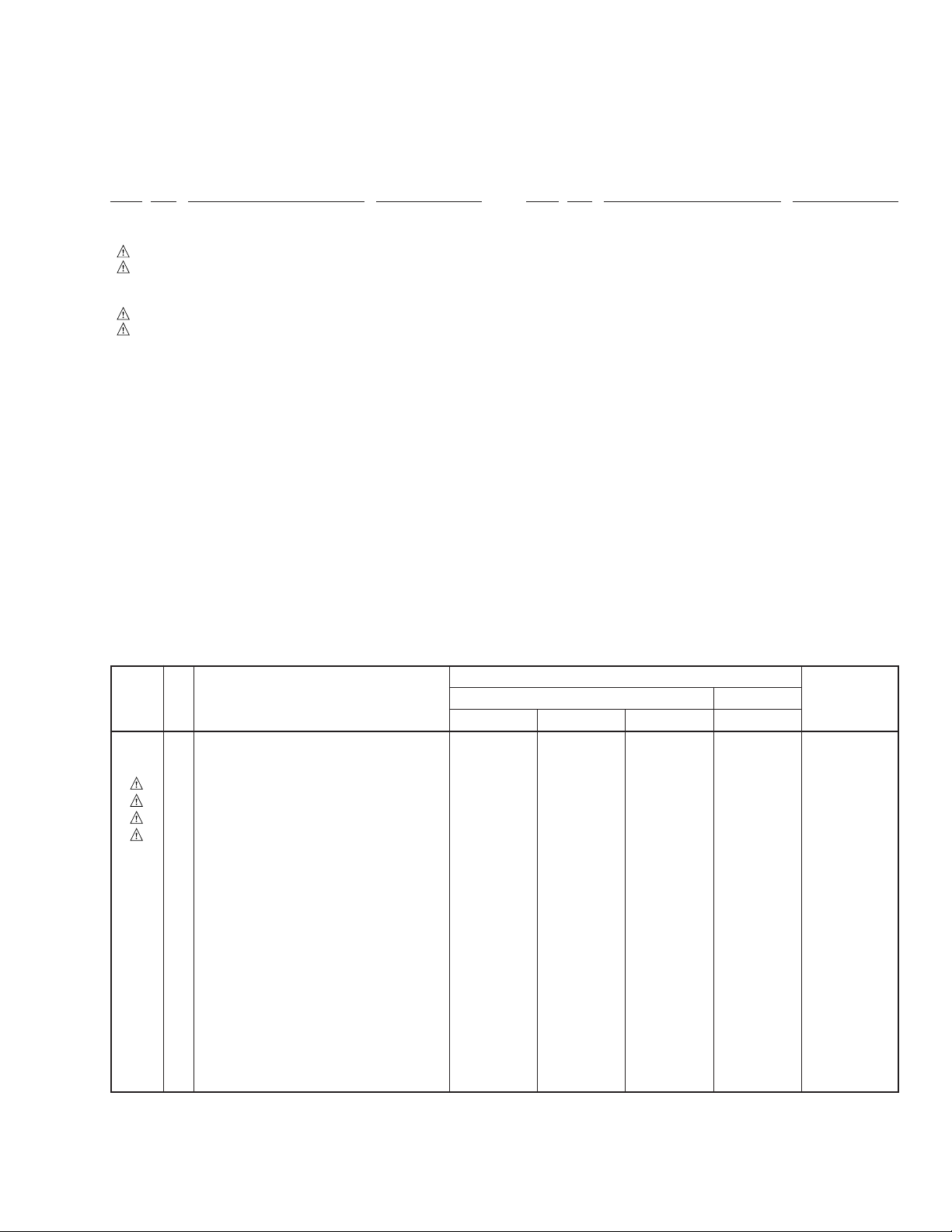
MJ-D707, MJ-17D
2.3 FRONT PANEL SECTION
Not used
Cut
23
1
5
23
6
23
20
2
12 (1/2)
14
15
Cut
24
11
4
12 (2/2)
18
Cut
16
22
A
3
8
A
10
13
12 (1/2)12 (2/2)
21
9
7
17
19
8
Page 9
(1) FRONT PANEL SECTION PARTS LIST
Mark No. Description Part No.
MJ-D707, MJ-17D
1 DISPLAY UNIT ASSY
2 CONTROL UNIT ASSY
3 HEADPHONE UNIT ASSY
4 Door Holder RAH2852
5 Door Cam RAH2853
6 Door Spring RBH1459
7 Name Plate AAM7004
8 HEADPHONE Knob PAC1707
9 LED Lens PNW2019
10 VOL Knob RAC2197
11 PLAY Button B RAC2204
12 Slide Knob B RAC2208
13 JOG Knob B RAC2210
14 PLAY MODE Button B RAC2212
15 REC MODE Button B RAC2214
16 SEARCH Button B RAC2216
17 Front Panel
18 Door
19 Display Window RAH2862
20 FL Sheet
21 Panel Stay B RNT1250
22 Screw ABA7009
23 Screw PPZ30P100FMC
24 Edge Guard RBK1078
See Contrast table (2)
See Contrast table (2)
See Contrast table (2)
See Contrast table (2)
See Contrast table (2)
See Contrast table (2)
(2) CONTRAST TABLE
MJ-D707/KU, MY, MY/GR/FR and MJ-17D/KU are constructed the same except for the following:
Part No.
Mark
No.
1 DISPLAY UNIT ASSY RWZ4310 RWZ4294 RWZ4294 RWZ4289
2 CONTROL UNIT ASSY RWZ4311 RWZ4295 RWZ4295 RWZ4290
3 HEADPHONE UNIT ASSY RWZ4312 RWZ4296 RWZ4296 RWZ4291
17 Front Panel RAH2870 RAH2859 RAH2859 RAH2860
18 Door RAH2861 RAH2861 RAH2861 RAH2851
20 FL Sheet RAH2863 RAH2855 RAH2855 RAH2863
Symbol and Description
MJ-D707 MJ-17D
KU MY MY/GR/FR KU
Remarks
9
Page 10
MJ-D707, MJ-17D
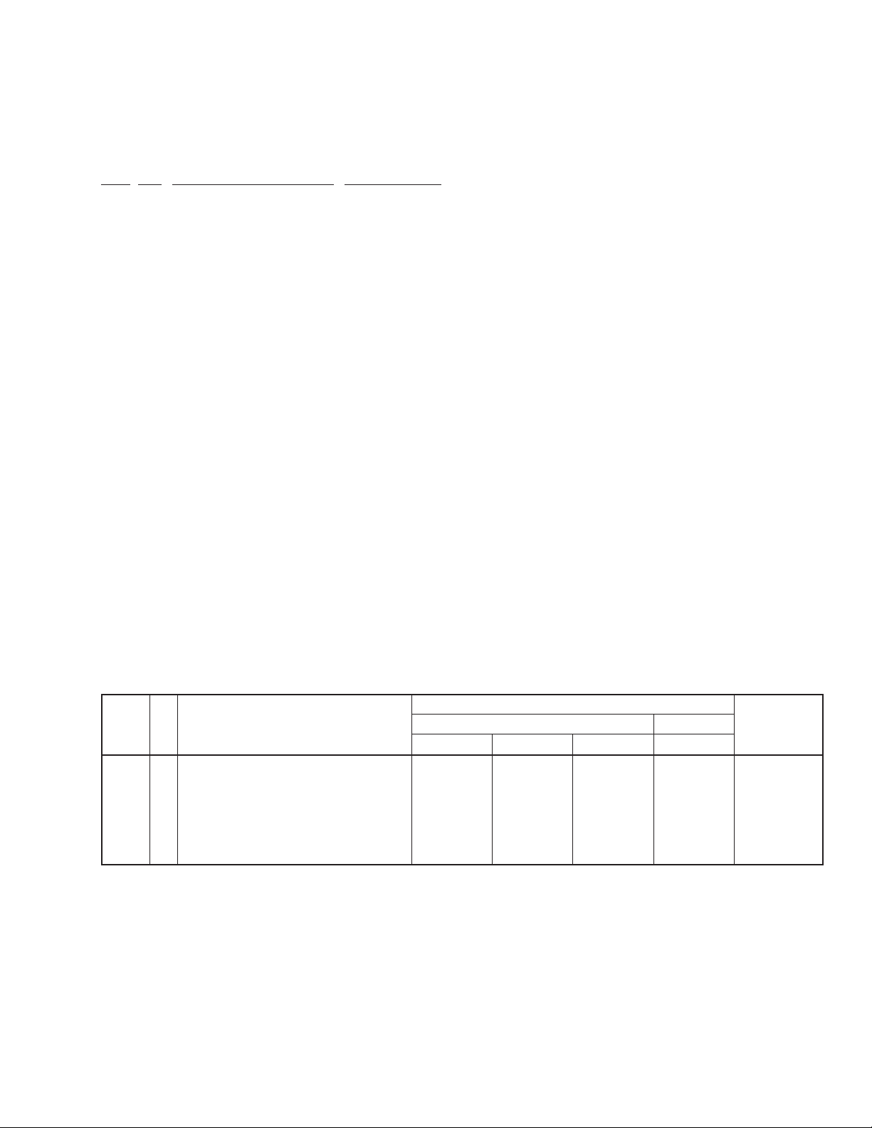
2.4 MD MECHANISM ASSY
19
21
20
18
37
6
51
52
8
37
34
7
E
4
9
17
A
37
53
24
14
37
13
12
40
15
40
26
E
F
5
G
41
16
35
F
11
B
27
10
36
C
28
44
33
31
23
40
H
25
39
29
3946
10
40
32
42
30
H
38
22
43
B
CN102
1
A
2
48
49
50 47
45
CN105
G
C
CN101
D
3
37
CN103
D
Page 11

MD MECHANISM ASSY PARTS LIST
Mark No. Description Part No.
MJ-D707, MJ-17D
Mark No. Description Part No.
1 CORE MAIN UNIT ASSY RWZ4271
2 CORE SW UNIT ASSY RWZ4272
3 Lead Card 7P RDD1399
4 Lead Wire RKP1814
5 Lever Spring RBH1463
6 Clamp Spring 1 RBK1074
7 Clamp Spring 2 RBK1075
8 Loading Belt REB1329
9 Lock Plate RNE1949
10 Loading Base RNK2312
11 Under Slider RNK2314
12 Gear Pulley RNK2316
13 Drive Gear RNK2317
14 Clutch Gear RNK2318
15 Flip Disk RNK2319
16 SW Lever RNK2320
17 Shutter Assy RXA1774
NSP 18 Upper Slider Assy RXA1775
19 Eject Spring RBH1461
20 Upper Slider RNK2313
21 Carrier RNK2315
22 Screw RBA1129
23 Spindle Spring RBH1460
24 Lifter SP RBH1462
25 Screw Guide RBK1072
41 Screw JGZ17P040FZK
42 Screw PMB20P040FMC
43 Servo Base Assy REA1283
NSP 44 Clamp Magnet RMF1002
NSP 45 Servo Base RNE1946
NSP 46 Disc Table RNK2305
NSP 47 Spindle Motor RXM1091
48 Carriage Motor Assy REA1284
49 Worm RNK2308
NSP 50 Carriage Motor RXM1090
51 Loading Motor Assy REA1285
52 DC Motor /0.75W PXM1010
53 CA Pulley (1) VNL1197
26 S. H. Spring RBK1073
27 Guide Shaft RLA1310
28 Lead Screw RLA1311
29 Shield Case RNE1950
30 Reference Plate RNK2306
31 S. Holder RNK2307
32 Worm Wheel RNK2309
33 Hook RNK2310
34 Head Lifter RNK2311
35 MD Head RPB1062
36 MD Pick-up RWY1018
37 Screw IPZ20P080FMC
38 Screw JFZ17P020FZK
39 Screw JGZ14P020FMC
40 Screw JGZ17P030FMC
11
Page 12
1
MJ-D707, MJ-17D
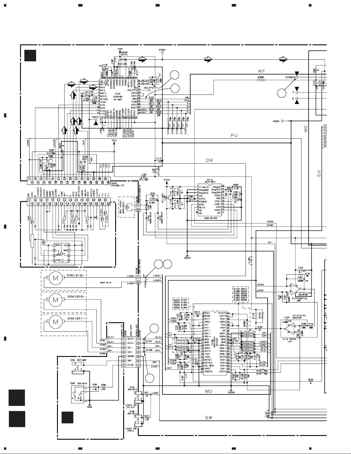
3. SCHEMATIC DIAGRAM
3.1 OVERALL CONNECTIONS
A
23
D
TRANS UNIT ASSY
(MJ-D707/KU : RWZ4313)
(MJ-D707/MY : RWZ4297)
(MJ-D707/MY/GR/FR : RWZ4297)
(MJ-17D/KU : RWZ4292)
AC POWER CORD
KU type : PDG1015
(AC120V/60Hz)
MY, MY/GR/FR type : PDG1003
(AC220–230V, 50/60Hz)
PARALLEL JUMPER
4
B
MD MECHANISM
ASSY
(RXA1773)
A
To
PICKUP
C
CORE MAIN
UNIT ASSY
(RWZ4271)
LEAD CARD
B
CORE SW
UNIT ASSY
(RWZ4272)
To
REC HEAD
LEAD CARD
JUMPER
(ORANGE)
(BLUE)
(BLACK)
(RED)
D
SLED
MOTOR
To
SPINDLE
MOTOR
To
To
MOTOR
LOADING
F
CONTROL UNIT ASSY
(MJ-D707/KU : RWZ4311)
(MJ-D707/MY : RWZ4295)
(MJ-D707/MY/GR/FR : RWZ4295)
PARALLEL
(MJ-17D/KU : RWZ4290)
12
1234
Page 13
5
678
MJ-D707, MJ-17D
Note : When ordering service parts, be sure to refer to "EXPLODED VIEWS and P AR TS LIST" or "PCB PAR TS LIST".
G
HEADPHONE UNIT ASSY
(MJ-D707/KU : RWZ4312)
(MJ-D707/MY : RWZ4296)
(MJ-D707/MY/GR/FR : RWZ4296)
(MJ-17D/KU : RWZ4291)
( )
C
MAIN UNIT ASSY
(MJ-D707/KU : RWZ4309)
(MJ-D707/MY : RWZ4293)
(MJ-D707/MY/GR/FR : RWZ4293)
(MJ-17D/KU : RWZ4288)
C
1/2,
C
2/2
PARALLEL
JUMPER
A
B
PARALLEL JUMPER PARALLEL JUMPER
E
DISPLAY UNIT ASSY
(MJ-D707/KU : RWZ4310)
(MJ-D707/MY : RWZ4294)
(MJ-D707/MY/GR/FR : RWZ4294)
(MJ-17D/KU : RWZ4289)
5
6
C
D
13
7
8
Page 14
1
23
MJ-D707, MJ-17D
3.2 CORE MAIN UNIT and CORE SW UNIT ASSEMBLIES
A
A
CORE MAIN
UNIT ASSY
(RWZ4271)
1
4
2
3
B
PICKUP
LOADING MOTOR
C
SLED MOTOR
SPINDLE MOTOR
INSIDE SW
YELLOW
BLACK
ORANGE
BLUE
BLACK
RED
1011
8
9
D
B
A
A : DISC PROTECT
B : DISC MEDIA DETECT
B
CORE SW
UNIT ASSY
14
1234
(RWZ4272)
Page 15
5
¶ 1 – - are waveform Nos. on pages 26 and 27.
678
MJ-D707, MJ-17D
SIGNAL ROUTE
: PLAYBACK SIGNAL
6
5
7
4
: REC SIGNAL
: OUTPUT DIGITAL AUDIO SIGNAL
: INPUT DIGITAL AUDIO SIGNAL
: RF SIGNAL
A
B
C
YB
0.01
(INSIDE)
C
CN401
D
R291–R293 : 47k
A
5
6
7
8
15
Page 16
MJ-D707, MJ-17D
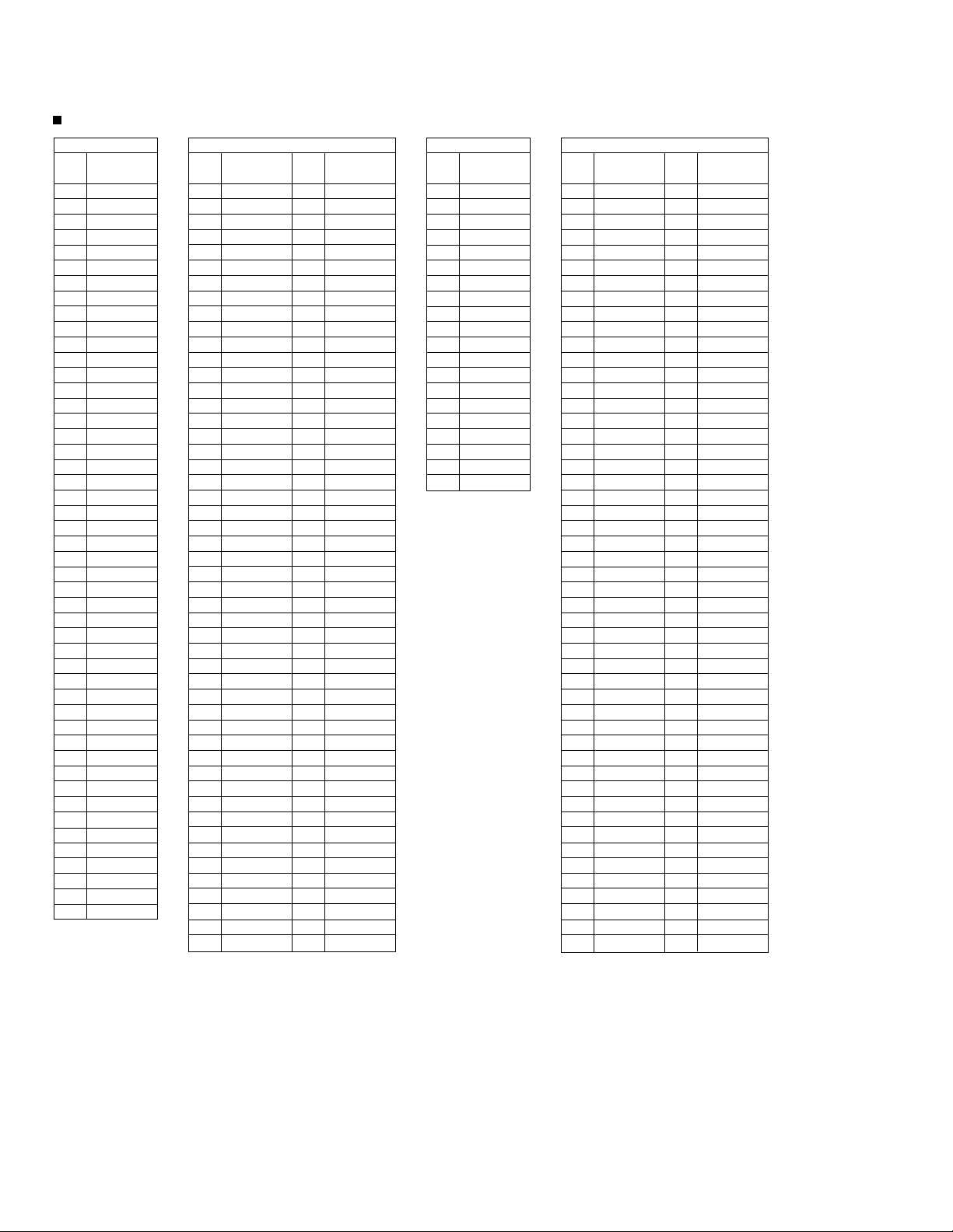
Voltages of CORE MAIN UNIT ASSY
PIN
NO.
1
2
3
4
5
6
7
8
9
10
11
12
13
14
15
16
17
18
19
20
21
22
23
24
25
26
27
28
29
30
31
32
33
34
35
36
37
38
39
40
41
42
43
44
45
46
47
48
IC101
VOLTAGE
0.78V
0.73V
0.77V
0.75V
1.61V
1.61V
0.75V
1.61V
1.61V
1.61V
1.61V
1.61V
3.19V
3.19V
0V
0V
3.19V
0V
0V
1.5V
3.2V
0V
0V
3.19V
2.0V
0V
1.40V
1.42V
1.40V
1.63V
1.61V
1.61V
0V
0V
0V
1.62V
0.59V
1.61V
1.61V
1.61V
1.61V
3.19V
0V
1.08V
1.61V
1.61V
0V
0.74V
PIN
NO.
1
2
3
4
5
6
7
8
9
10
11
12
13
14
15
16
17
18
19
20
21
22
23
24
25
26
27
28
29
30
31
32
33
34
35
36
37
38
39
40
41
42
43
44
45
46
47
48
49
50
VOLTAGE
IC102
1.53V
3.18V
1.65V
0V
1.42V
0V
1.59V
1.41V
1.97V
1.39V
1.64V
3.18V
0V
0V
0V
0V
1.69V
1.52V
1.70V
1.47V
1.47V
1.65V
1.54V
1.69V
1.51V
0.82V
2.0V
2.0V
1.81V
1.4V
0.82V
1.67V
1.67V
1.67V
2.86V
1.32V
2.23V
0V
2.4V
1.2V
1.5V
0V
2.0V
3.0V
1.2V
1.2V
0.02V
3.04V
1.57V
0.05V
PIN
NO.
51
52
53
54
55
56
57
58
59
60
61
62
63
64
65
66
67
68
69
70
71
72
73
74
75
76
77
78
79
80
81
82
83
84
85
86
87
88
89
90
91
92
93
94
95
96
97
98
99
100
VOLTAGE
1.59V
0V
0V
1.59V
1.8V
0V
0V
0V
0V
0V
0.56V
3.18V
0V
1.5V
1.5V
3.2V
1.6V
3.2V
0V
1.6V
1.6V
1.48V
0V
0V
1.68V
1.82V
1.59V
0.35V
0.02V
3.2V
3.2V
0.02V
0.03V
1.9V
1.56V
3.1V
3.2V
0V
3.19V
0.5V
0.5V
0.5V
0.5V
0.9V
0.5V
0.5V
0.5V
0.8V
3.18V
0.06V
PIN
NO.
1
2
3
4
5
9
10
11
12
13
14
15
16
17
18
22
23
24
25
26
IC103
VOLTAGE
1.2V
1.2V
3.0V
2.0V
0V
2.23V
1.32V
2.86V
1.67V
3.18V
1.67V
1.67V
1.67V
2.86V
1.32V
2.23V
2.4V
1.2V
1.5V
0V
PIN
NO.
1
2
3
4
5
6
7
8
9
10
11
12
13
14
15
16
17
18
19
20
21
22
23
24
25
26
27
28
29
30
31
32
33
34
35
36
37
38
39
40
41
42
43
44
45
46
47
48
49
50
IC104
VOLTAGE
0V
0V
0.22V
0.03V
1.29V
2.21V
3.13V
0V
0V
0V
0V
3.03V
1.43V
0V
1.57V
3.2V
3.19V
3.1V
0.03V
0V
0V
3.18V
3.2V
0V
2.67V
3.19V
0V
0V
2.4V
0.24V
0V
0.3V
3.2V
1.56V
1.0V
0V
2.77V
0V
3.18V
0.02V
3.19V
3.2V
0V
0.05V
3.18V
3.19V
0.51V
0.4V
0.3V
0.55V
PIN
NO.
51
52
53
54
55
56
57
58
59
60
61
62
63
64
65
66
67
68
69
70
71
72
73
74
75
76
77
78
79
80
81
82
83
84
85
86
87
88
89
90
91
92
93
94
95
96
97
98
99
100
VOLTAGE
0.54V
0.6V
0.6V
0.6V
0V
0V
0V
0V
3.2V
0V
0V
3.2V
0V
0V
3.2V
0V
0V
0V
0V
0V
0V
3.1V
3.2V
0V
0V
3.2V
0V
0V
0V
3.2V
0V
3.19V
0V
3.19V
0V
3.18V
3.2V
0V
1.03V
1.6V
0.56V
1.49V
1.49V
0.68V
0.61V
0V
0.53V
3.2V
3.2V
0V
16
Page 17
MJ-D707, MJ-17D
PIN
NO.
1
2
3
4
5
6
7
8
9
10
11
12
13
14
15
16
17
18
19
20
21
22
23
24
25
26
27
28
29
30
31
32
33
34
35
36
37
38
39
40
41
42
IC106
VOLTAGE
1.6V
0.49V
1.61V
4.99V
4.99V
1.61V
1.62V
2.46V
2.51V
0V
0V
2.54V
2.45V
1.62V
1.62V
1.61V
3.17V
0V
1.61V
1.61V
1.61V
1.61V
1.36V
1.36V
1.61V
1.61V
1.63V
2.41V
2.55V
2.47V
2.48V
0V
0V
2.79V
2.18V
0V
1.69V
5.0V
4.99V
1.67V
1.69V
1.69V
PIN
NO.
1
2
3
4
5
6
7
8
9
10
11
12
13
14
15
16
PIN
NO.
1
2
3
4
5
IC108
VOLTAGE
2.47V
2.63V
4.87V
2.63V
1.59V
0V
0V
4.87V
0V
2.25V
4.94V
4.94V
4.94V
4.94V
3.12V
4.94V
IC114
VOLTAGE
0V
4.19V
3.21V
2.81V
0V
PIN
NO.
1
2
3
4
5
6
7
8
9
10
11
12
13
14
PIN
NO.
1
2
3
4
5
6
7
8
9
10
11
12
13
14
15
16
17
18
19
20
IC109
VOLTAGE
2.77V
2.77V
3.2V
1.58V
1.58V
1.56V
0V
0V
0V
0V
0V
0V
0V
3.2V
IC116
VOLTAGE
4.98V
0V
0V
4.99V
3.2V
0V
0.03V
3.18V
0V
0V
0V
0.22V
0V
0.25V
0.25V
2.82V
0.16V
4.94V
2.82V
1.33V
PIN
NO.
1
2
3
4
5
6
7
8
IC110
VOLTAGE
0V
3.2V
0V
3.2V
0V
0.11V
0V
0V
PIN
NO.
1
2
3
4
5
6
7
8
IC112
VOLTAGE
1.66V
1.62V
1.62V
0V
1.67V
1.67V
1.67V
3.19V
PIN
NO.
1
2
3
4
5
6
7
8
9
10
11
12
13
14
IC113
VOLTAGE
4.95V
3.96V
0V
0V
0V
0V
0V
0V
4.94V
4.12V
3.19V
0V
0V
4.94V
17
Page 18
1
D
e
23
MJ-D707, MJ-17D
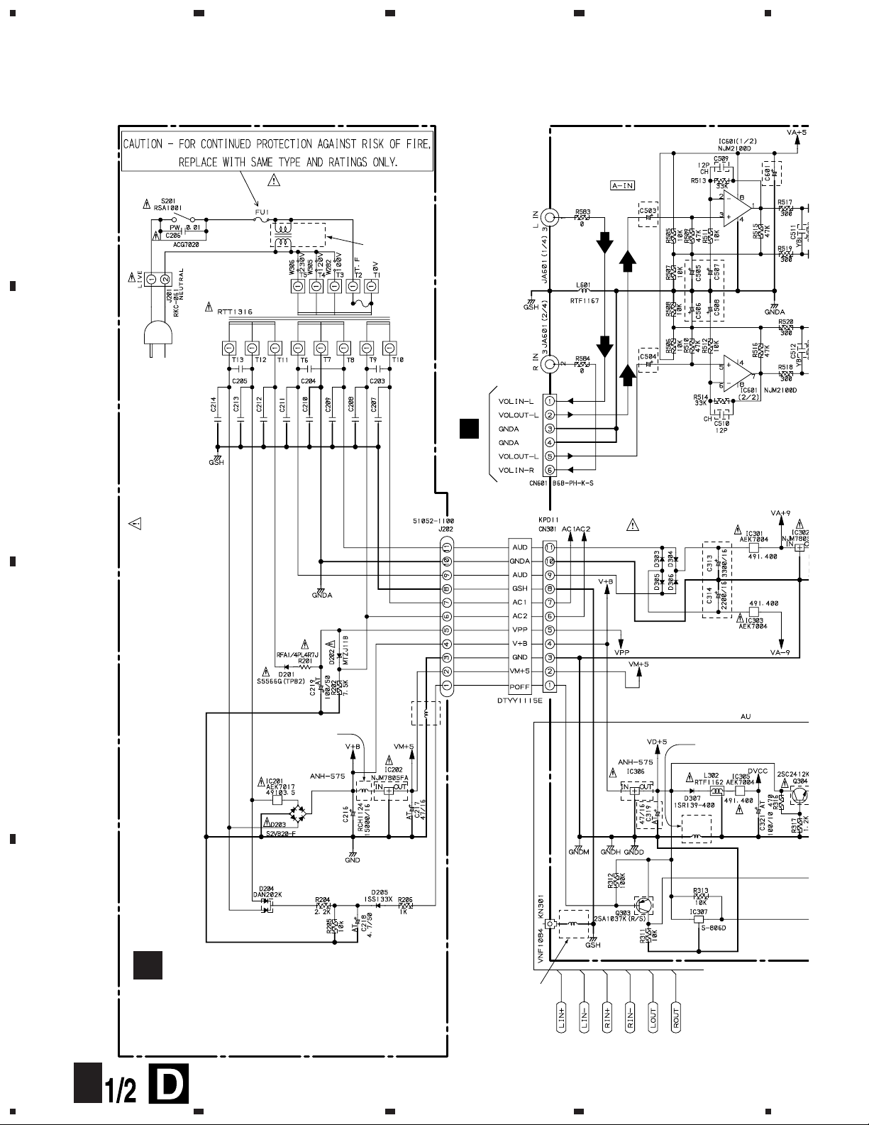
3.3 MAIN UNIT ASSY (1/2) and TRANS UNIT ASSY
4
A
S201 : POWER
H201, H202
: AKR1004
JUMPER
KU type : W305
MY, MY/GR/FR type : W306
POWER TRANSFORMER
B
FU1 FUSE
KU type : REK1075 (1A/125V)
MY, MY/GR/FR type : REK1019 (500mA/250V)
L201
VTL-262
MY and MY/GR/FR
types only
E
C503, C504
MJ-D707/KU : CEAT470M16
other models : CEBA220M25
JA601 : RKB1032
C50
MJoth
J704
C203–C205, C207–C214 : CFTLA, 0.1
AC POWER CORD
KU type : PDG1015
(AC120V/60Hz)
MY, MY/GR/FR type : PDG1003
(AC220–230V, 50/60Hz)
D303–D306 : S5566G(TPB2)
C313, C314
MJ-D707/KU : CEAT
other models : PCH1120 (C313)
: PCH1121 (C314)
C315, C319
MJ-D707/KU : CEAT470M16
C
L202 : RTF1167
MY and MY/GR/FR
L203 : RTF1167
MY and MY/GR/FR
types only
HEAT SINK
D
D
TRANS UNIT ASSY
(MJ-D707/KU : RWZ4313)
types only
MY and MY/GR/FR
types only
HEAT SINK
BA05T
L305
RTF1167
other models : PCH1123
MY and MY/GR/FR
types only
L304
RTF1167
(MJ-D707/MY : RWZ4297)
(MJ-D707/MY/GR/FR : RWZ4297)
(MJ-17D/KU : RWZ4292)
18
C
1234
Page 19
5
¶ % is waveform Nos. on page 27.
678
MJ-D707, MJ-17D
C505 – C508, C601
MJ-D707/KU : CEAT470M16
other models : RCH1133
SIGNAL ROUTE
: PLAYBACK SIGNAL
: REC SIGNAL
C551, C552, C559, C560
MJ-D707/KU : CEAT
other models : CEBA
2.2/50
470k470k
2.2/50
C
1/2
IC603 : NJM4580D
MAIN UNIT ASSY (1/2)
(MJ-D707/KU : RWZ4309)
(MJ-D707/MY : RWZ4293)
(MJ-D707/MY/GR/FR : RWZ4293)
(MJ-17D/KU : RWZ4288)
18
A
B
120 (C313)
121 (C314)
T470M16
1123
Y/GR/FR
LINE MUTE
100 (1/4W)
68k
68k
100 (1/4W)
CAUTION : FOR CONTINUED PROTECTION AGAINST RISK OF FIRE.
REPLACE ONLY WITH SAME TYPE NO. 49103.5 MFD, BY
LITTELFUSE INK. FOR IC201(AEK7017).
CAUTION : FOR CONTINUED PROTECTION AGAINST RISK OF FIRE.
REPLACE ONLY WITH SAME TYPE NO. 491.400 MFD, BY
LITTELFUSE INK. FOR IC301, IC303, IC305(AEK7004).
C
G
J901
D
C
5
6
7
8
19
Page 20
1
F
MJ-D707, MJ-17D
3.4 MAIN UNIT ASSY (2/2)
A
17
23
4
B
DSP (built-in 20 bit ADC/DAC)
13
C614
MJ-D707/KU : CEAT221M6R3
other models : VCH1081
15
12
14
C604, C612, C616
MJ-D707/KU : CEAT470M16
other models : VCH1081
C
16
D
L306 : RT
MY and M
types only
20
E
J702
E
J703
C
1234
Page 21
5
¶ = – # are waveform Nos. on pages 26 and 27.
678
MJ-D707, MJ-17D
C
2/2
MAIN UNIT ASSY (2/2)
(MJ-D707/KU : RWZ4309)
(MJ-D707/MY : RWZ4293)
(MJ-D707/MY/GR/FR : RWZ4293)
(MJ-17D/KU : RWZ4288)
L406
RTF1167
A
SIGNAL ROUTE
: PLAYBACK SIGNAL
: REC SIGNAL
: OUTPUT DIGITAL AUDIO SIGNAL
: INPUT DIGITAL AUDIO SIGNAL
B
RKB1021
MY and MY/GR/FR
types only
R455 : MY, MY/GR/FR types only
L307
RTF1167
MY and MY/GR/FR
types only
C
KU type only
D
L306 : RTF1167
MY and MY/GR/FR
types only
A
CN104
C
5
6
7
8
21
Page 22

1
(
(
(
(
23
MJ-D707, MJ-17D
3.5 DISPLAY UNIT, CONTROL UNIT and HEADPHONE UNIT ASSEMBLIES
A
B
4
PDG222B
C
SYSTEM CONTROLER
CN402
(MD µ-COM)
(MD µ-COM)
(MD µ-COM)
C
C
CN403
CHASSIS
D
22
1234
Page 23

5
678
MJ-D707, MJ-17D
A
G
HEADPHONE UNIT ASSY
(MJ-D707/KU : RWZ4312)
(MJ-D707/MY : RWZ4296)
(MJ-D707/MY/GR/FR : RWZ4296)
(MJ-17D/KU : RWZ4291)
B
C
CN602
E
DISPLAY UNIT ASSY
(MJ-D707/KU : RWZ4310)
(MJ-D707/MY : RWZ4294)
(MJ-D707/MY/GR/FR : RWZ4294)
(MJ-17D/KU : RWZ4289)
C
CN601
C903, C904 : CCSQCH, 100P
RDF1155(1/2) BLACK
CHASSIS
F
CONTROL UNIT ASSY
(MJ-D707/KU : RWZ4311)
(MJ-D707/MY : RWZ4295)
(MJ-D707/MY/GR/FR : RWZ4295)
(MJ-17D/KU : RWZ4290)
HEADPHONE OUT
DISPLAY UNIT ASSY
S701 : JOG DIAL
S702 : FAST REVERSE
S703 : NAME
S704 : EDIT/NO
S705 : FAST FORWARD
S706 : SYNCHRO REC
S707 : RECORD
S708 : STOP
S709 : MD EJECT
S710 : PAUSE
S711 : PLAY
S712 : INPUT SELECTOR
CONTROL UNIT ASSY
S801 : TIMER
S802 : DISPLAY/CHARA
S803 : NAME CLIP
S804 : DIGITAL NR
S805 : REC MODE
S806 : TIME SKIP
S807 : A-B
S808 : REPEAT
S809 : PLAY MODE
C
D
23
5
6
7
8
Page 24

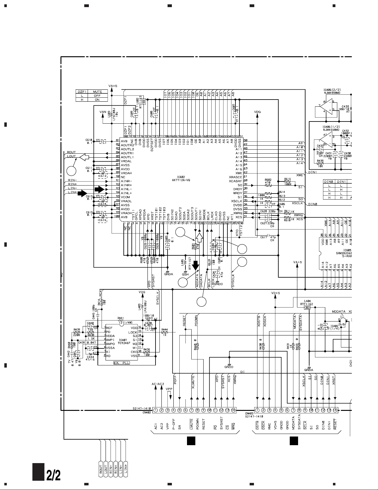
MJ-D707, MJ-17D
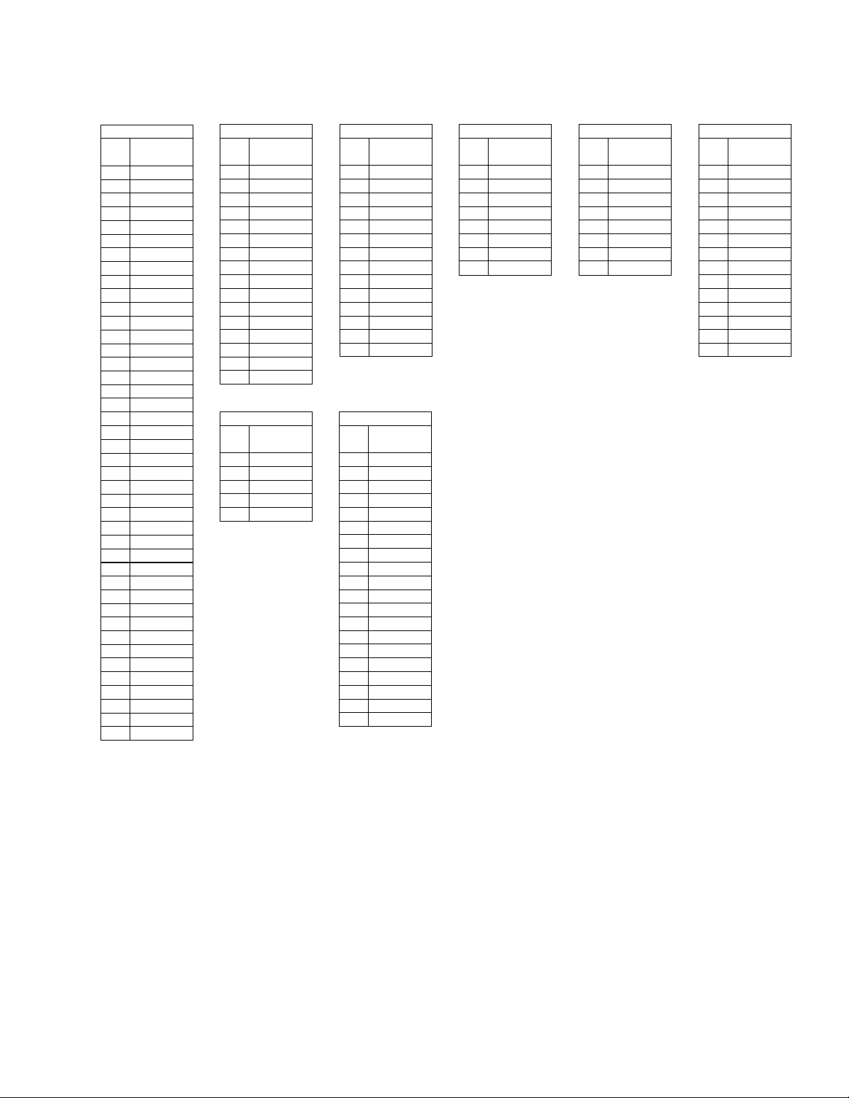
Voltages of MAIN UNIT ASSY
PIN
NO.
1
2
3
4
5
6
7
8
9
10
11
12
13
14
PIN
NO.
1
2
3
4
5
6
7
8
IC401
VOLTAGE
3.2V
3.2V
5.0V
1.6V
1.6V
2.5V
0V
2.5V
1.6V
1.6V
1.6V
1.0V
1.0V
5.0V
IC406
VOLTAGE
4.6V
5.0V
0V
0V
0V
4.6V
4.6V
5.0V
PIN
NO.
1
2
3
4
5
6
7
8
9
10
11
12
13
14
PIN
NO.
1
2
3
4
5
6
7
8
9
10
11
12
13
14
15
16
IC402
VOLTAGE
0V
0V
0V
0V
0V
0V
0V
2.5V
1.6V
1.6V
1.6V
1.0V
1.0V
5.0V
IC407
VOLTAGE
2.5V
2.7V
5.0V
2.7V
1.7V
0V
0V
5.0V
0V
2.3V
5.0V
5.0V
5.0V
5.0V
5.0V
5.0V
PIN
NO.
1
2
3
4
5
6
7
8
9
10
11
12
13
14
PIN
NO.
1
2
3
4
5
6
7
8
PIN
NO.
1
2
3
4
5
6
7
8
IC403
VOLTAGE
2.5V
2.5V
2.5V
3.4V
0V
5.0V
0V
0V
4.7V
4.7V
0V
0V
4.5V
5.0V
IC601
VOLTAGE
2.55V
2.55V
2.55V
0V
2.55V
2.55V
2.55V
5.06V
IC604
VOLTAGE
0V
0V
0V
0V
0V
0V
0V
8.89V
PIN
NO.
1
2
3
4
5
6
7
8
9
10
11
12
13
14
15
16
PIN
NO.
1
2
3
4
5
6
7
8
PIN
NO.
1
2
3
4
5
6
7
8
9
10
11
12
13
14
15
16
17
18
19
20
21
22
23
24
25
26
27
28
IC404
VOLTAGE
0V
4.3V
5.0V
5.0V
5.0V
3.4V
5.0V
0V
0V
0V
0V
0V
0V
5.0V
0V
5.0V
IC603
VOLTAGE
0.028V
0.013V
0.013V
–9.31V
0.013V
0.013V
0.027V
8.49V
IC605
VOLTAGE
2.5V
2.5V
2.5V
2.5V
2.5V
2.5V
2.5V
2.5V
2.5V
4.7V
2.5V
2.5V
2.5V
0V
2.5V
2.5V
2.5V
2.5V
2.5V
0V
0.5V
2.5V
2.5V
2.5V
2.5V
2.5V
4.8V
5.0V
PIN
NO.
1
2
3
4
5
6
7
8
9
10
11
12
13
14
15
16
17
18
19
20
21
22
23
24
25
26
27
28
29
30
31
32
33
34
35
36
37
38
39
40
41
42
43
44
45
46
47
48
49
50
IC602
VOLTAGE
0V
0V
0V
0V
0V
0V
5.0V
5.0V
0V
0V
0V
5.0V
0V
0V
0V
0V
0V
0V
0V
0V
0V
2.5V
2.5V
0V
5.0V
0V
0V
2.3V
2.6V
5.0V
0.15V
4.9V
0V
5.0V
4.9V
0.18V
4.8V
4.8V
0.15V
1.7V
0.3V
3.3V
2.5V
2.5V
3.3V
2.5V
2.5V
2.5V
2.5V
2.5V
PIN
NO.
51
52
53
54
55
56
57
58
59
60
61
62
63
64
65
66
67
68
69
70
71
72
73
74
75
76
77
78
79
80
81
82
83
84
85
86
87
88
89
90
91
92
93
94
95
96
97
98
99
100
VOLTAGE
0V
5.0V
2.5V
2.5V
2.5V
2.5V
2.5V
2.5V
2.5V
2.5V
2.5V
2.5V
2.5V
2.5V
2.5V
2.5V
2.5V
2.5V
2.5V
2.5V
0V
5.0V
5.0V
0V
5.0V
0V
5.02V
5.02V
5.02V
0V
5.02V
2.5V
2.5V
2.5V
2.5V
0V
0V
5.02V
5.02V
5.02V
2.5V
2.5V
2.5V
2.5V
2.51V
0V
0V
5.02V
5.02V
5.02V
24
Page 25

Voltages of DISPLAY UNIT ASSY
IC701
PIN
NO.
1
2
3
4
5
6
7
8
9
10
11
12
13
14
15
16
17
18
19
20
21
22
23
24
25
26
27
28
29
30
31
32
33
34
35
36
37
38
39
40
41
42
43
44
45
46
47
48
49
50
VOLTAGE
– 28.0V
– 28.0V
5.0V
0V
5.0V
0V
5.0V
5.0V
5.0V
0V
4.9V
5.0V
0V
4.9V
5.0V
5.0V
5.0V
5.0V
0.1V
4.9V
2.5V
4.6V
1.6V
0V
4.9V
0V
0V
5.0V
5.0V
5.0V
5.0V
5.0V
5.0V
0V
5.0V
5.0V
0V
5.0V
2.3V
2.4V
0V
5.0V
0V
5.0V
– 30.3V
0V
0V
0V
0V
– 30.3V
PIN
NO.
51
52
53
54
55
56
57
58
59
60
61
62
63
64
65
66
67
68
69
70
71
72
73
74
75
76
77
78
79
80
81
82
83
84
85
86
87
88
89
90
91
92
93
94
95
96
97
98
99
100
VOLTAGE
– 23.3V
– 11.9V
– 14.2V
– 18.9V
– 16.6V
– 14.5V
– 23.5V
– 21.1V
– 23.3V
– 12.3V
– 14.4V
– 23.5V
– 18.8V
– 18.8V
– 12.2V
– 14.4V
– 14.3V
– 12.1V
– 16.6V
– 16.7V
– 12.1V
– 16.4V
– 16.5V
– 18.8V
– 12.1V
– 14.4V
– 23.5V
– 19.1V
– 21.2V
– 14.4V
– 18.9V
– 18.9V
– 16.6V
– 16.7V
– 16.7V
– 29.5V
– 28.0V
– 28.0V
5.0V
– 28.0V
– 28.0V
– 28.0V
– 28.0V
– 28.0V
– 28.0V
– 28.0V
– 28.0V
– 28.0V
– 28.0V
– 28.0V
MJ-D707, MJ-17D
25
Page 26

MJ-D707, MJ-17D
Waveforms
Note: The encircled numbers denote measuring point in the schematic diagram and the PCB connection diagram.
IC101-pin35 (ADIPO)
1
(CORE MAIN UNIT ASSY)
MODE: PLAY
DISC: GGF1328 (MMD–212)
DC500mV/div., 10 µSec/div.
IC102-pin50 (EFMO)
4
(CORE MAIN UNIT ASSY)
MODE: REC
DISC: GGF1328 (MMD–212)
DC1V/div., 0.2 µSec/div.
–– GND
–– GND
IC101-pin30 (WBO)
2
(CORE MAIN UNIT ASSY)
MODE: PLAY
DISC: GGF1328 (MMD–212)
DC1V/div., 10 µSec/div.
IC102-pin75 (FE MON)
5
(CORE MAIN UNIT ASSY)
MODE: PLAY
DISC: TGTS1 or MMD–110
DC100mV/div., 2mSec/div.
–– GND
–– GND
IC102-pin1 (EFM MON)
3
(CORE MAIN UNIT ASSY)
MODE: PLAY
DISC: TGTS1 or MMD–110
DC500mV/div., 0.5mSec/div.
Measurement Method
FE MON
39 kΩ
REFO
(MD Mechanism Assy TP)
–– GND
To Oscilloscope
820pF
IC102-pin77 (TE MON)
6
(CORE MAIN UNIT ASSY)
MODE: PLAY
DISC: TGTS1 or MMD–110
DC500mV/div., 2mSec/div.
CN103-pin1 (SLD +)
8
(CORE MAIN UNIT ASSY)
MODE: PLAY
DC500mV/div., 2mSec/div.
–– GND
–– GND
Measurement Method
TE MON
9
39 kΩ
REFO
(MD Mechanism Assy TP)
CN103-pin4 (SP +)
(CORE MAIN UNIT ASSY)
MODE: PLAY
DC500mV/div., 5mSec/div.
To Oscilloscope
820pF
–– GND
IC102-pin54 (TES01)
7
(CORE MAIN UNIT ASSY)
MODE: STOP
DC2V/div., 10 µSec/div.
CN105-pin1 (LOAD –)
10
(CORE MAIN UNIT ASSY)
MODE: STOP
DC1V/div., 1mSec/div.
–– GND
–– GND
26
Page 27

MJ-D707, MJ-17D
CN105-pin1 (LOAD –)
11
(CORE MAIN UNIT ASSY)
MODE: EJECT
DC1V/div., 1mSec/div.
CN602-pin20 (DA DATA)
14
(MAIN UNIT ASSY)
MODE: PLAY (1 kHz, 0 dB)
DC2V/div., 0.5 µSec/div.
–– GND
–– GND
IC602-pin28 (SYS CLK)
12
(MAIN UNIT ASSY)
MODE: STOP
DC2V/div., 50nSec/div.
IC602-pin23 (LRCK)
15
(MAIN UNIT ASSY)
MODE: PLAY (1 kHz, 0 dB)
DC2V/div., 10 µSec/div.
–– GND
–– GND
IC602-pin19 (AD DATA)
13
(MAIN UNIT ASSY)
MODE: REC (ANALOG)
DISC: GGF1328 (MMD-212)
DC2V/div., 0.5 µSec/div.
IC602-pin22 (BCLK)
16
(MAIN UNIT ASSY)
MODE: PLAY (1 kHz, 0 dB)
DC2V/div., 0.2 µSec/div.
–– GND
–– GND
CN602-pin85 (LOUT)
17
(MAIN UNIT ASSY)
MODE: PLAY (1 kHz, 0 dB)
DC2V/div., 0.2mSec/div.
–– GND
IC603-pin1
18
MODE: PLAY (1 kHz, 0 dB)
(MAIN UNIT ASSY)
AC2V/div., 0.2mSec/div.
–– GND
27
Page 28

1
23
MJ-D707, MJ-17D
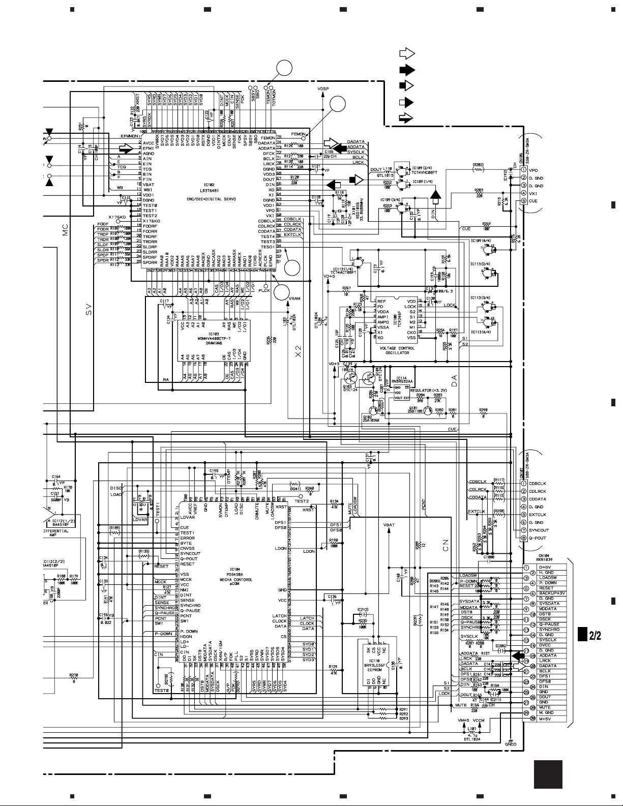
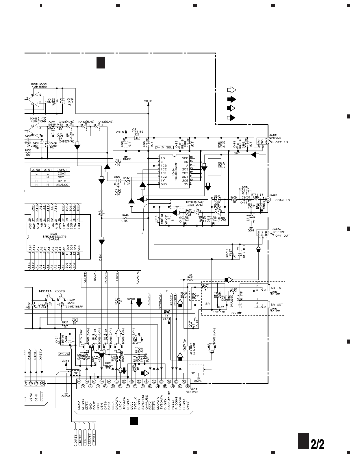
4. PCB CONNECTION DIAGRAM
A
NOTE FOR PCB DIAGRAMS :
1. Part numbers in PCB diagrams match those in the schematic
diagrams.
2. A comparison between the main parts of PCB and schematic
diagrams is shown below.
Symbol In PCB
Diagrams
BCE
BCE
D
Symbol In Schematic
Diagrams
BCEBCE
BCE
DGGSS
BCE
DGS
Part Name
Transistor
Transistor
with resistor
Field effect
transistor
4
3. The parts mounted on this PCB include all necessary parts for
several destinations.
For further information for respective destinations, be sure to
check with the schematic diagram.
4. View point of PCB diagrams.
Connector
Capacitor
SIDE A
P.C.Board
Chip Part
SIDE B
B
Resistor array
3-terminal
regulator
4.1 CORE SW UNIT ASSEMBLY
B
CORE SW UNIT ASSY
C
SPINDLE MOTOR
SLED MOTOR
A
CN103
D
SIDE A
(RNP1721-B)
SIDE B
28
1234
Page 29

1
234
4.2 CORE MAIN UNIT ASSEMBLY
A
CORE MAIN UNIT ASSY
1
2
5
6
8
3
B
CN701
MJ-D707, MJ-17D
¶ 1 – - are waveform Nos. on pages 26 and 27.
A
7
SIDE A
B
1011
9
IC101
IC106 IC102 IC103 IC104 IC114
(RNP1721-B)
Q101
Q102
SIDE B
C
LOADING
MOTOR
IC113
C
CN401
PICKUP
ASSY
REC
HEAD
4
IC112 IC108 IC113
1
2
Q103
IC110 IC116
3
(RNP1721-B)
IC109
Q104
29
4
D
Page 30

1
23
MJ-D707, MJ-17D
4.3 MAIN UNIT and TRANS UNIT ASSEMBLIES
4
A
B
SIDE A
D
TRANS UNIT ASSY
C
MAIN UNIT ASSY
H
J10
C
D
NEUTRAL
LIVE
AC POWER
CORD
IC201
(RNP1726-C)
A
CN104
30
IC305 IC301 IC303
1234
Page 31

5
678
MJ-D707, MJ-17D
¶ = – % are waveform Nos. on page 25.
H
J1001
17
18
E
SIDE A
A
J102
B
4
12
15
16
14
(RNP1726-C)
E
J102
3 IC405 IC307
13
E
J103
G
J901
C
D
31
5
6
7
8
Page 32

1
MJ-D707, MJ-17D
SIDE B
A
C
MAIN UNIT ASSY
B
23
4
C
(RNP1726-C)
D
IC604 Q504
Q502
IC605
Q503 IC602 IC407 IC406 IC404IC403
Q501
Q604 Q601
Q603 Q605 Q303
Q602
IC401
IC402
32
1234
Page 33

5
678
MJ-D707, MJ-17D
SIDE B
A
D
TRANS UNIT ASSY
B
Q304
5
(RNP1726-C)
6
C
D
33
7
8
Page 34

1
23
MJ-D707, MJ-17D
4.4 DISPLAY UNIT and CONTROL UNIT ASSEMBLIES
A
E
DISPLAY UNIT ASSY
B
4
SIDE A
SIDE A
C
F
CONTROL UNIT ASSY
(RNP1726-C)
SIDE B
D
(RNP1726-C)
34
1234
Page 35

5
678
MJ-D707, MJ-17D
C
CN402
SIDE B
C
CN403
C
(RNP1726-C)
CN601
SIDE A
F
CONTROL UNIT ASSY
A
B
(RNP1726-C)
SIDE B
5
6
E
DISPLAY UNIT ASSY
35
7
8
C
D
Page 36

1
MJ-D707, MJ-17D
4.5 HEADPHONE UNIT ASSEMBLY
A
G
HEADPHONE UNIT ASSY
B
23
C
CN602
4
(RNP1726-C)
SIDE A
C
SIDE B
D
36
1234
Page 37

MJ-D707, MJ-17D
5. PCB PARTS LIST
NOTES : Parts marked by “ NSP ” are generally unavailable because they are not in our Master Spare Parts List.
The mark found on some component parts indicates the importance of the safety factor of the part.
Therefore, when replacing, be sure to use parts of identical designation.
When ordering resistors, first convert resistance values into code form as shown in the following examples.
Ex. 1 When there are 2 effective digits (any digit apart from 0), such as 560 ohm and 47k ohm (tolerance is shown by
J = 5%, and K = 10%).
560 Ω = 56 × 10
47k Ω = 47 × 10
0.5 Ω = R50 ...................................................................... RN2H Â 5 0 K
1 Ω = 1R0 ......................................................................... RS1P 1 Â 0 K
Ex. 2 When there are 3 effective digits (such as in high precision metal film resistors).
5.62k Ω = 562 × 10
LIST OF WHOLE PCB ASSEMBLIES
Mark Remarks
NSP MD MECHANISM ASSY RXA1773 RXA1773 RXA1773 RXA1773
Symbol and Description
CORE UNIT ASSY RWM2041 RWM2041 RWM2041 RWM2041
CORE MAIN UNIT ASSY RWZ4271 RWZ4271 RWZ4271 RWZ4271
CORE SW UNIT ASSY RWZ4272 RWZ4272 RWZ4272 RWZ4272
1
= 561................................................... RD1/4PU 5 6 1 J
3
= 473 .................................................. RD1/4PU 4 7 3 J
1
= 5621 ........................................... RN1/4PC 5 6 2 1 F
Part No.
MJ-D707 MJ-17D
KU MY MY/GR/FR KU
NSP MOTHER UNIT ASSY RWM2051 RWM2048 RWM2048 RWM2047
MAIN UNIT ASSY RWZ4309 RWZ4293 RWZ4293 RWZ4288
DISPLAY UNIT ASSY RWZ4310 RWZ4294 RWZ4294 RWZ4289
CONTROL UNIT ASSY RWZ4311 RWZ4295 RWZ4295 RWZ4290 ∗1
HEADPHONE UNIT ASSY RWZ4312 RWZ4296 RWZ4296 RWZ4291 ∗2
TRANS UNIT ASSY RWZ4313 RWZ4297 RWZ4297 RWZ4292
∗1 Although RWZ4311, RWZ4295 and RWZ4290 are different in part number, they have the same service parts.
∗2 Although RWZ4312, RWZ4296 and RWZ4291 are different in part number, they have the same service parts.
CONTRAST OF PCB ASSEMBLIES
D
TRANS UNIT ASSY
RWZ4313, RWZ4297 and RWZ4292 are constructed the same except for the following:
Mark Symbol and Description
L201 Not used VTL–262 Not used
L202, L203 Not used RTF1167 Not used
E
DISPLAY UNIT ASSY
RWZ4313 RWZ4297 RWZ4292
RWZ4310, RWZ4294 and RWZ4289 are constructed the same except for the following:
Part No.
Remarks
Mark
Symbol and Description
Part No.
RWZ4310 RWZ4294 RWZ4289
R798 RS1/10S104J Not used Not used
R799 Not used RS1/10S104J RS1/10S104J
Remarks
37
Page 38

MJ-D707, MJ-17D
MAIN UNIT ASSY
C
RWZ4309, RWZ4293 and RWZ4288 are constructed the same except for the following:
Mark
Symbol and Description
Part No.
RWZ4309 RWZ4293 RWZ4288
D401 DAP202K Not used DAP202K
D402 1SS133X Not used 1SS133X
L304–L307, L406 Not used RTF1167 Not used
C313 CEAT332M16 PCH1120 PCH1120
(3300µF/16V) (3300µF/16V)
C314 CEAT222M16 PCH1121 PCH1121
(2200µF/16V) (2200µF/16V)
C315, C319 CEAT470M16 PCH1123 PCH1123
(470µF/6.3V) (470µF/6.3V)
C419 CKSQYF104Z25 Not used CKSQYF104Z25
C503, C504 CEAT470M16 CEBA220M25 CEBA220M25
C505–C508, C601 CEAT470M16 RCH1133 RCH1133
(100µF/10V) (100µF/10V)
C551, C552 CEAT2R2M50 CEBA2R2M50 CEBA2R2M50
C559, C560 CEAT470M16 CEBA470M10 CEBA470M10
C604, C612, C616 CEAT470M16 VCH1081 VCH1081
(220µF/10V) (220µF/10V)
C614 CEAT221M6R3 VCH1081 VCH1081
(220µF/10V) (220µF/10V)
C619, C621 CEAT470M16 PCH1124 PCH1124
(47µF/50V) (47µF/50V)
R412, R437 RS1/10S102J Not used RS1/10S102J
R413 RS1/10S274J Not used RS1/10S274J
R455 Not used RS1/10S0R0J Not used
R618 RS1/10S622J RS1/10S101J RS1/10S101J
Remarks
JA405, JA406 JACK (Remote Control) RKN1004 Not used RKN1004
PARTS LIST FOR MJ-D707/KU
Mark No. Description Part No. Mark No. Description Part No.
A
CORE MAIN UNIT ASSY
SEMICONDUCTORS
IC112 BA4510F
IC116 BD7910FV
IC110 BR93LC56F
IC101 IR3R55M
IC102 LR376481
IC106 M56758FP
IC103 M5M4V4400CTP-7
IC104 PD5450A
IC114 RN5RG32AA
IC113 TC74ACT08FT
IC109 TC74VHC08FT
IC108 TC9246F
Q102 2SA1036K
Q101 2SB1188
Q103, Q104 DTC124EU
D101, D102 SB02-09CP
COILS AND FILTERS
L101, L103, L104, L107 (4.7 µH) DTL1024
L110 QTL1015
L108 (47 µH) RTL1003
L102 (0.47 µH) RTL1007
SWITCHES AND RELAYS
S101, S102 RSF1012
CAPACITORS
C115 CCSQCH101J50
C119, C120 CCSQCH120J50
C146 CCSQCH121J50
C125 CCSQCH150J50
C141–C144, C155 CCSQCH220J50
C174–C178 CCSQCH271J50
C194 CCSQCH331J50
C139 CEV101M4
C131, C166 CEV101M6R3
C147, C148, C201 CEV470M6R3
38
Page 39

MJ-D707, MJ-17D
Mark No. Description Part No. Mark No. Description Part No.
C112 CEV4R7M35
C193 CKSQYB102K50
C126, C1000 CKSQYB103K50
C153, C154 CKSQYB153K50
C158 CKSQYB222K50
C196–C198 CKSQYB223K50
C103, C145 CKSQYB273K50
C171 CKSQYB332K50
C149, C170 CKSQYB333K50
C106, C159 CKSQYB472K50
C127 CKSQYB474K16
C156, C157 CKSQYB562K50
C151, C152, C160, C162 CKSQYB821K50
C130, C132, C134, C137, C138 CKSQYF104Z25
C161, C163, C164, C173, C195 CKSQYF104Z25
C202–C205 CKSQYF104Z25
C101, C102, C104, C108 CKSQYF105Z16
C113, C114, C116–C118 CKSQYF105Z16
C121, C122, C124, C128 CKSQYF105Z16
C135, C136, C140, C165, C169 CKSQYF105Z16
C207, C208 CKSQYF105Z16
C123 CKSQYF473Z25
C105, C107 CKSQYF474Z16
RESISTORS
R105 RS1/8S270J
Other Resistors RS1/10S J
OTHERS
CN104 30P CONNECTOR RKN1039
X101 (33.8688MHz) RSS1055
CN105 ZR CONNECTOR S2B-ZR-SM3A
CN102 2P CONNECTOR S2B-ZR-SM3A-R
CN101 CONNECTOR SFV28R-1ST
CN103 CONNECTOR SFW7R-2ST
IC406 NJM4558MD
IC603 NJM4580D
IC302 NJM7805FA
IC307 S-806D
IC605 SRM2B256SLMX70
IC404 TC74HC153AF
IC401, IC402 TC74HCT08AF
IC403 TC74HCU04AF
IC407 TC9246F
Q303 2SA1037K
Q304 2SC2412K
Q501–Q504 2SD2114K
Q601, Q602 DTA124EK
Q603–Q605 DTC124EK
D307 1SR139-400-TA
D308, D402, D602 1SS133X
D401, D603 DAP202K
D303–D306 S5566G(TPB2)
COILS AND FILTERS
L403, L603 LFA100J
L301, L302, L404 RTF1162
L602 RTF1163
L401 RTF1165
L402, L601, L604, L605, L607 RTF1167
CAPACITORS
C445 CCSQCH101J50
C509, C510 CCSQCH120J50
C440 CCSQCH150J50
C411, C413, C446 CCSQCH220J50
C433, C627, C628 CCSQCH221J50
C412, C423, C617 CCSQCH470J50
C321, C403, C406, C415, C417 CEAT101M10
C421, C435, C443 CEAT101M10
C551, C552 CEAT2R2M50
C614 CEAT221M6R3
B
CORE SW UNIT ASSY
SWITCHES AND RELAYS
S701 RSF1009
S702 RSF1010
RESISTORS
All Resistors RS1/10S J
OTHERS
CN701 CONNECTOR SFW7R-1ST
MAIN UNIT ASSY
C
SEMICONDUCTORS
IC301, IC303, IC305 (400mA/125V) AEK7004
IC405 (200mA/125V) AEK7023
IC602 AK7712A-VQ
IC306 BA05T
IC604 M5218AFP
IC601 NJM2100D
C314 CEAT222M16
C410 CEAT330M50
C313 CEAT332M16
C315, C319, C444, C503–C508 CEAT470M16
C559, C560, C565, C566, C601 CEAT470M16
C604, C612, C616, C619, C621 CEAT470M16
C324 CEAT471M6R3
C624 CEAT4R7M50
C442 CFTYA474J50
C432, C447, C561, C562 CKSQYB102K50
C625, C626 CKSQYB102K50
C441, C449 CKSQYB103K50
C553–C558 CKSQYB152K50
C430, C431 CKSQYB222K50
C511, C512 CKSQYB332K50
C409, C429 CKSQYF103Z50
C401, C402, C404, C405, C414 CKSQYF104Z25
C416, C418–C420, C422, C434 CKSQYF104Z25
C603, C605–C611, C613, C615 CKSQYF104Z25
C629 CKSQYF105Z16
C438, C439 CKSQYF473Z25
C323 (1.00F/5.5V) RCH1152
39
Page 40

MJ-D707, MJ-17D
Mark No. Description Part No. Mark No. Description Part No.
RESISTORS
R579, R580, R616, R617 RD1/4PU101J
R441 RD1/4PU120J
R559, R560 RN1/10SE1202D
Other Resistors RS1/10S J
OTHERS
CN602 3P JUMPER CONNECTOR 52147-0310
CN402, CN403 52147-1410
CN601 KR CONNECTOR B6B-PH-K-S
JA401 OPTICAL LINK IN GP1F32R
JA404 OPTICAL LINK OUT GP1F32T
CN301 11P JUMPER CONNECTOR KPD11
JA403 1P JACK RKB1021
JA601 4P JACK with SHIELD PLATE RKB1032
JA405, JA406 JACK RKN1004
CN401 30P CONNECTOR VKN1206
KN301, KN601 EARTH METAL FITTING VNF1084
E
DISPLAY UNIT ASSY
14P JUMPER CONNECTOR
HEAT SINK ANH-575
PCB BINDER VEF1040
SEMICONDUCTORS
IC701 PDG222B
CAPACITORS
C801 CKSQYF104Z25
RESISTORS
All Resistors RS1/10S J
OTHERS
6P CABLE HOLDER 51048-0600
G
HEADPHONE UNIT ASSY
COILS AND FILTERS
L901–L903 RTF1167
CAPACITORS
C901, C902 CKSQYF104Z25
C903, C904 CCSQCH101J50
RESISTORS
VR901 (500 Ω–B) RCV1123
Other Resistors RS1/10S J
OTHERS
901 3P CABLE HOLDER 51048-0300
J901 3P JUMPER WIRE D20PYY0310E
JA901 HEADPHONE JACK RKN1002
SWITCHES AND RELAYS
S712 RSB1027
S701 RSC1003
S702–S711 VSG1009
CAPACITORS
C701 CEAL220M6R3
C707, C708, C712 CKSQYB103K50
C703, C709 CKSQYF103Z50
C702, C704–C706, C710, C711 CKSQYF104Z25
RESISTORS
VR701 (50 kΩ–A) RCV1118
Other Resistors RS1/10S J
OTHERS
J701 6P PARALLEL WIRE D20PYY0615E
J702, J703 14P JUMPER WIRE D20PYY1425E
V701 FL TUBE RAW1164
J704 6P CONNECTOR ASSY RKP1812
X701 (8.388MHz) RSS1042
F
CONTROL UNIT ASSY
6P CABLE HOLDER 51048-0600
REMOTE RECEIVER UNIT GP1U27X
SEMICONDUCTORS
D801 SLP9118C51H
SWITCHES AND RELAYS
S801 RSH1041
S802–S809 VSG1009
D
TRANS UNIT ASSY
SEMICONDUCTORS
IC201 (3.5A/125V) AEK7017
IC202 NJM7805FA
D205 1SS133X
D204 DAN202K
D202 MTZJ11B
D203 S2VB20
D201 S5566G (TPB2)
SWITCHES AND RELAYS
S201 RSA1001
CAPACITORS
C206 (10000pF/AC250V) ACG7020
C219 CEAT101M50
C217 CEAT470M16
C218 CEAT4R7M50
C203–C205, C207–C214 CFTLA104J50
C216 (15000pF/16V) RCH1124
RESISTORS
R201 RFA1/4PL4R7J
Other Resistors RS1/10S J
OTHERS
H201, H202 FUSE CLIP AKR1004
CABLE HOLDER (11P) 51052-1100
HEAT SINK ANH-575
TERMINAL RKC-061
40
Page 41

6. ADJUSTMENT
JIGS AND MEASURING INSTRUMENTS
MJ-D707, MJ-17D
Thermometer
Oscilloscope
Optical Power Meter
Test Disc
For servo system adjustment ............................................. GGF1328 (MMD-212)
For recording/playback inspection...................GGF1328 (MMD-212), GGF1277,
Jitter Meter
6.1 NECESSARY ADJUSTMENT POINTS
Exchange
PICKUP
Exchange
Servo Base Assy (SPINDLE MOTOR)
Exchange
CORE MAIN UNIT ASSY
TGYS1 (or MMD-110), Commercial discs
Adjustment pointsWhen
3 , 4
3 , 4
= Page 44, 45
= Page 44, 45
= Page 44, 45
4
Exchange
MD HEAD
Exchange
Loading Mechanism Assy
Exchange
Servo Mechanism Assy
Exchange
MD Mechanism Assy
(Loading Mechanism Assy +
Servo Mechanism Assy)
3 , 4
3 , 4
= Page 44, 45
= Page 44, 45
41
Page 42

MJ-D707, MJ-17D
6.2 TEST MODE
There are two test modes: test mode 1 for main unit operation check
and test mode 2 for MD mechanism assy adjustment and check.
6.2.1 Test Mode 1 (main unit operation check)
How to enter into test mode 1
1) Hold the “ENTER” key and the “STOP” key depressed and press the POWER switch.
2) SYSTEM TEST will be displayed on the FL display.
Operation check for the operation keys
Operation Keys FL Display Contents
REC (¶)
PLAY (3)
STOP (7) Same operation as in normal mode
JOG (4, ¢)
CUE (¡)
REV (1)
EJECT (0) Disc ejection (no TOC writing)
DIGITAL-NR DSP OK ! ! Normal DSP IC operation
DSP ERROR1 Communication between the DSP IC and the system controller is not
possible.
DSP ERROR2 Calculation in the DSP IC not correct
Operation check for other keys
When each key is pressed, display according to the following table shall be made on the FL display.
Operation Keys FL Display
OFF SYSTEM TEST
TIMER SW REC Entire FL lit
PLAY Entire FL not lit
A–B A–B
REPEAT REPEAT
PLAY MODE PLAY MODE
TIME SKIP TIME SKIP
NAME CLIP NAME C L I P
Operation Keys FL Display
JOG (Push) ENT ER
EDIT/NO EDI T /NO
NAME NAME
SYNCHRO REC SYNCHRO REC
Cancellation of Test Mode 1
Press the POWER switch.
DISPLAY/CHARA DISP
REC MODE REC MODE
42
Page 43

MJ-D707, MJ-17D
TEMP
µ-com Measuring value
11.6 to 16.9 +1 to +3
17.0 to 22.3 0 to +2
22.4 to 27.6 –1 to +1
27.7 to 33.0 0 to –2
33.1 to 38.4 –1 to –3
79
7A
7B
7C
7D
hex=
( – )
Room Temperature
[ T (°C) ]
µ-com Set value
When the
microcomputer
value is
+
–
6.2.2 Test Mode 2 (MD Mechanism Assy Adjustment, Check)
1 Temperature Check (Please perform this check soon after the power has been switched on.)
Note: When IC101 (RF-AMP) or IC104 (mechanical controller) has been exchanged or when a correction changing VD+3 has been made,
be sure to correctly perform all steps up to step 7.
Step No. Operation Keys and Operation Method FL Display Status Remarks
1 Power ON while holding the ENTER key and the EJECT Test mode
PLAY key depressed.
2 Press the NAME CLIP key. TEMP The microcomputer starts measuring.
3 When is 80 or more at this time, the adjustment End
is OK (step 4 and following can be omitted).
When is 80 (not passed) TEMP 8 0 80 is the default value (unadjusted).
4 Measure the ambient temperature T (°C) andcheck
hat the measuring value ( ) is within the standard
in regard to the microcomputer set value ( ).
Note: When the indication of the measuring value
( ) is not stable, and the ambient temperature
T (°C) is 25 °C or less, set to the lower value.
When the ambient temperature is over 25 °C, set to
the higher value.
: Measuring
value
: Set value
2 Laser Power Check
Step No. Operation Keys and Operation Method FL Display Status Remarks
5 Change with the TIME SKIP key (UP) and the TEMP 7B 7B
A-B key (DOWN).
6 Press the EDIT/NO key. No Disc Writing to EEPROM is made and
return is made automatically from
test mode to normal mode.
1 Power ON while holding the ENTER key and the EJECT Test mode
PLAY key depressed. 780 nm
2 Press the NAME key. ppw PLAY power output status
3 Measure the laser power with an optical power meter. ppw
4 At this time, check that the measuring value (PLAY ppw May be omitted.
power) meets the standard value of the table on the
right.
Note: When the standard value on the right is applied,
the numerical value immediately after entry into test
mode 2 shall be taken as the standard.
5 Press the NAME key. rpw REC power output status
6 At this time, check that the measuring value (REC rpw
power) meets the standard value of the table on the
right.
7 Press the STOP key. The LD goes out.
µ-com
Measuring value
( – ) (mW)
( – ) (mW)
TEMP
hex = Standard Value
+02 to +04 0.69±0.12
–01 to +01 0.67±0.1
–02 to –04 0.63±0.1
hex = Standard Value
+02 to +04 6.18±0.93
–01 to +01 5.79±0.87
–02 to –04 5.47±0.82
µ-com
Set value
Laser Wavelength:
43
Page 44

MJ-D707, MJ-17D
Ocsilloscope
b
a
470p
470p
100kΩ
100kΩ
3 Grating Adjustment
Step No. Operation Keys and Operation Method FL Display Status Remarks
1 Power ON while holding the ENTER key and the PLAY EJECT Test mode
key depressed.
2 Insert the test disc GGF1328 (MMD-212). LOADING
GRT AJST Grating adjustment status
3 Press the PLAY key. LON : Playback is started in tracking open
LAg : status. (The servo is closed only for
GEG : focus and spindle.)
4 Connect an oscilloscope according to the following GRT AJST Lissajous waveform a:b = Within 3:1
connection diagram and loosen the screw A at the side
of the adjustment hole. Turn the hole with a screwdriver
until the Lissajous waveform becomes as shown in the
figure, and then tighten the screw A.
5 Press the STOP key. Adjustment end
Connection Diagram
Lissajous waveform
a:b = Within 3:1
CORE MAIN UNIT ASSY
EOUT
FOUT
SIDE A
Adjustment
Hole
Screw A
Adjustment
Point
REFO
4 Preliminary Adjustment
Step No. Operation Keys and Operation Method FL Display Status Remarks
1 Power ON while holding the ENTER key and the PLAY EJECT Test mode
key depressed.
2 Insert the test disc GGF1328 (MMD-212). LOADING
3 Press the REC MODE key (until RST YOBI is displayed). RST YOBI
4 Press the PLAY key. Preliminary adjustment result display
5 Press the REC MODE key several times and display GTG :
the GTG (GROOV TRACKING GAIN) value.
6 Use the TIME SKIP key (UP) and the A-B key (DOWN) GTG : 4
to adjust the value of to 4 or more.
GRT AJST
mode
44
Page 45

MJ-D707, MJ-17D
4 Preliminary Adjustment
Step No. Operation Keys and Operation Method FL Display Status Remarks
7 Press the STOP key. RST YOBI Return to menu display
8 Press the REC MODE key (until AUT YOBI is displayed). AUT YOBI Preliminary adjustment mode
9 Preliminary adjustment starts when the PLAY key is HAo :
pressed. LAg :
PTG :
|
Can't ADJ. Defective adjustment
(problem with the servo system)
COMPLETE Adjustment end
10 Press the STOP key. AUT YOBI Return to menu display
11 Press the EDIT/NO key. EEPROM W Writing to the EEPROM
Toc Reading
GGF1328
(MMD-212)
Note: When this adjustment is performed after defocus adjustment has been performed, defocus is returned to the initial status, and defocus
adjustment must be performed.
5 Normal adjustment
Step No. Operation Keys and Operation Method FL Display Status Remarks
1 Power ON while holding the ENTER key and the PLAY EJECT Test mode
key depressed.
2 Insert the test disc GGF1328 (MMD-212). LOADING
GRT AJST
3 Press the REC MODE key (until AUTO AJST is displayed). AUTO AJST Normal adjustment mode
4 Normal adjustment starts when the PLAY key is pressed. PEG :
HAG:
|
Can't ADJ. Defective adjustment
(problem with the servo system)
COMPLETE Adjustment end
5 Press the STOP key. AUTO AJST Return to menu display
6 Defocus adjustment
Step No. Operation Keys and Operation Method FL Display Status Remarks
1 Power ON while holding the ENTER key and the EJECT Test mode
PLAY key depressed.
2 Insert the test disc GGF1328 (MMD-212). LOADING
GRT AJST
3 Press the REC MODE key deFO AJST
(until deFO AJST is displayed).
4 Press the PLAY key. PEG : Defocus mode is entered, and after automatic
of c
Deforcus Value C1 Error Value
5 Check the jitter value and end the adjustment when
the intermediate jitter value is 29 nsec or less.
6 Press the NAME CLIP key. of+04 c0032 The C1 error with application of a focus offset of
FESpp : execution of normal adjustment, the C1 error at
of000c0015 the time of focus offset 0 is displayed.
about 0.4 µm on the + side is displayed.
The jitter value (J+) at this time is recorded.
45
Page 46

MJ-D707, MJ-17D
6 Defocus adjustment
Step No. Operation Keys and Operation Method FL Display Status Remarks
7 Press the NAME CLIP key. of-04 c0020 The C1 error with application of a focus offset of
about 0.4 µm on the – side is displayed.
The jitter value (J–) at this time is recorded.
8 When J+ is larger than J-, press the REC MODE of+04 c0032
key and display the C1 error when the focus offset
is applied up to +0.4 µm.
(Do nothing when J- is larger than J+.)
9 Change the value with CUE (1)/REV (1) until of+04 c0032 When the smaller offset of the jitter value has
the value becomes the same. of+03 c0025 been corrected mistakenly, press the NAME key
of+02 c0020 and return to step 4.
10 Press the PLAY key. COMPLETE The mean value of the changed set value and
the offset of the other setting limit is written into
the EEPROM as the compensation offset.
11 Power OFF Test mode is ended.
Connection diagram
Jitter Meter
LEVEL
GND
CORE MAIN UNIT ASSY
JITTER
REFO
SIDE A
EFM MON
7 Jitter/C1 Error Check at the time of Playback
Step No. Operation Keys and Operation Method FL Display Status Remarks
1 Power ON while holding the ENTER key and the EJECT Test mode
PLAY key depressed.
2 Insert the test disc GGF1328 (MMD-212). LOADING
GRT AJST
3 Perform “ Normal Adjustment ” (step 3, step 4). AUTO AJST
4 Press the NAME CLIP key. TEST PLAY TEST PLAY mode
5 Press the NAME key and display the inner ADRES 0050
circumference address.
6 Press the PLAY key and display the C1 error for a0050 c0015 Check that the jitter value meets the standard
the inner circumference. value of the following table.
GGF1328 (MMD-212) jitter value
Inner circumference 31 nsec or less
Intermediate circumference
Outer circumference 29 nsec or less
29 nsec or less
7 Press the REC key. A0062 c0013 Seven data are acquired, the largest and the
AVE. c0012 smallest value are discarded, and fixed display
is made for the mean value of the remaining
five data. Check that this value is 200 or less.
46
Page 47

MJ-D707, MJ-17D
7 Jitter/C1 Error Check at the time of Playback
Step No. Operation Keys and Operation Method FL Display Status Remarks
8 Press the REC key. a006F c0017 The fixed display of the C1 error is ended.
9 Press the STOP key. TEST PLAY
10 Press the NAME key and display the inner ADRES 0050
circumference address.
11 Press the NAME CLIP key and display the ADRES 03C0
intermediate circumference address. a03C0 c0009
Perform steps 6 to 9 in this condition. TEST PLAY
12 Press the NAME key and display the inner ADRES 0050
circumference address.
13 Press the NAME CLIP key twice to display the ADRES 0700
outer circumference address. a0700 c0008
Perform steps 6 to 9 in this condition. TEST PLAY
14 Press the EJECT key, eject the test disc EJECT
GGF1328 (MMD-212), and insert TGYS1 (or LOADING
MMD-110.) GRT AJST
15 Perform steps 3 to 13 and check the jitter/C1 a0062 c0009 Check that the jitter value meets the standard
error with the test disc TGYS1 ( or MMD-110). a03d2 c0007 value of the following table.
a0712 c0006
TGYS1 ( or MMD-110) jitter value
Inner circumference 29 nsec or less
Intermediate circumference
Outer circumference 27 nsec or less
27 nsec or less
Intermediate
and
outer
circumference
may be
omitted.
16 Press the EJECT key. EJECT The test disc TGYS1 ( or MMD-110) is ejected.
17 Power OFF Test mode is ended.
Jitter Meter
LEVEL
GND
CORE MAIN UNIT ASSY
JITTER
REFO
SIDE A
EFM MON
Connection diagram
47
Page 48

MJ-D707, MJ-17D
Jitter/C1 Error Check at the time of Recording/Playback
Step No. Operation Keys and Operation Method FL Display Status Remarks
1 Power ON while holding the ENTER key and the EJECT Test mode
PLAY key depressed.
2 Insert the test disc (GGF1277). LOADING
GRT AJST
3 Perform “ Normal Adjustment ” (step 3, step 4). AUTO AJST
4 Press the NAME CLIP key twice. TEST REC TEST REC mode
5 Press the NAME key and display the inner a0050 pw0D
circumference address.
6 When the PLAY key is pressed, TEST REC starts, a0069 pw0D
and when 25 addresses or more have been sent, TEST REC
stop by pressing the STOP key.
7 Press the NAME key and display the inner a0050 pw0D
circumference address.
8 Press the NAME CLIP key and display the a03C0 pw0D
intermediate circumference.
9 Perform step 6. a03D9 pw0D
TEST REC
10 Press the NAME key and display the inner a0050 pw0D
circumference address.
11 Press the NAME CLIP key twice and display the a0700 pw0D
outer circumference address.
12 Perform step 6. a0719 pw0D
TEST REC
13 Press the NAME CLIP key. TEST PLAY TEST PLAY mode
14 Perform steps 5 to 13 of “ Jitter/C1 Error Check a0069 c0009 Check the jitter/C2 error at the inner/
at the time of Playback ”. a03D9 c0007 intermediate/outer circumference of GGF1277,
At the time of self-recording, wait for seven a0719 c0006 and check that the jitter value satisfies the
addresses after TEST PLAY start, and then press standard value of the following table.
the REC key and enter into mean value mode.
(Good recording may not be possible for several
addresses at the beginning.)
Note:When the initial address (0050) part of
the inner circumference (or intermediate/
outer circumference) has been used 1000
times or more, press the CUE key and
shift the address by 10hex. (The address
is shifted (up to 10 times) according to the
use frequency of the disc.)
GGF1277 jitter value
Inner circumference 33 nsec or less
Intermediate circumference
Outer circumference 31 nsec or less
31 nsec or less
Intermediate
and
outer
circumference
may be
omitted.
15 Press the EJECT key. EJECT The test disc (GGF1277) is ejected.
16 Power OFF Test mode is ended.
Jitter Meter
LEVEL
GND
CORE MAIN UNIT ASSY
JITTER
REFO
SIDE A
EFM MON
Connection diagram
48
Page 49

7. GENERAL INFORMATION
MJ-D707, MJ-17D
7.1 PARTS
7.1.1 IC
M5M4V4400CTP-7 (IC103: CORE MAIN UNIT ASSY)
DRAM
Pin Assignment (Top view)
DQ1
DQ2
RAS
A9
A0
A1
A2
A3
VCC
1
2
3
W
4
5
9
10
11
12
13
26
17
Block Diagram
VSS
25
DQ4
24
DQ3
23
CAS
22
OE
18
A8
A7
16
A6
15
A5
14
A4
Pin Function
No. Name Description
1 DQ1
Data Input/Output
2 DQ2
3 W Write control input
4 RAS Line address strobe input
5 A9 Address input
6
|
8
9A0
| | Address input
12 A3
13 Vcc Power supply voltage (+3.3 V)
¶ The information shown in the list is basic information and may
not correspond exactly to that shown in the schematic diagrams.
No. Name Description
14 A4
| | Address input
18 A8
19
|
21
22 OE Output-enable input
23 CAS Column address strobe input
24 DQ3
Data Input/Output
25 DQ4
26 Vss Ground (0 V)
CAS
RAS
A0
A1
A2
A3
A4
A5
A6
A7
A8
A9
23
4
3
W
9
10
11
12
14
15
16
17
18
5
Address Buffer
Clock Generation Circuit
Column Decoder
Sense Reflesh Amp.
Line Decoder
Input/Output
Control Circuit
Memory Cell
(4194304bits)
Input
Buffer
Output
Buffer
Vcc (3.3V)
13
Vss (0V)
26
1
DQ1
2
DQ2
DQ3
24
DQ4
25
OE
22
49
Page 50

MJ-D707, MJ-17D
M56758FP (IC106: CORE MAIN UNIT ASSY)
5-channel Actuator Driver
Pin Assignment (Top view)
1
REG+
REGB
2
IN1+
3
4
VBS1
Vm1
5
IN1–
6
7
OUT1
8
VM1–
9
VM1+
10
GND
GND
VM2+
VM2–
OUT2
IN2–
IN2+
MUTE1
MUTE2
SS. GND
VREF
VREFO
M56758FP
11
12
13
14
15
16
17
18
19
20
21
42
41
40
39
38
37
36
35
34
33
32
31
30
29
28
27
26
25
24
23
22
CH3IN
OUT3
IN3–
VBS2
Vm2
IN3+
N.C.
VM3–
VM3+
GND
GND
VM4+
VM4–
VM5+
VM5–
OUT5
IN5–
IN5+
IN4+
IN4–
OUT4
Block Diagram
3
IN1+
6
IN1–
7
OUT1
9
VM1+
VM1–
8
12
VM2+
VM2–
13
14
OUT2
15
IN2–
16
IN2+
VREFO
21
20
VREF
2
REGB
1
REG+
Vm1
5 4
VBS1
–
VBS1
VREG
+
VBS1
+
–
CH1
×5
–
+
VBS1
+
–
CH2
×5
–
+
VBS1
–
+
E2
VBS1
–
+
VREF
–
+
R
R
Vrefm1
1.25V
19 17
–
+
BIAS
MUTE ON
VBS1
Vm1
VREFO
L: Open
CH
1 to 4
VBS2
39
Vm2
H: Sleep
VBS1
CH5
18 10 11 32 33
–
+
Vrefm2
SLEEP
TSD
Vm2
38
VBS2
VBS2
VBS2
VBS2
CH3
×8
CH4
×8
VBS2
CH5
×8
VBS2
E3
E4
E5
R
R
40
–
+
–
+
–
+
IN3–
37
IN3+
41
OUT3
42
CH3IN
+
34
VM3+
–
–
35
VM3–
+
+
31
VM4+
–
–
30
VM4–
+
22
OUT4
23
IN4–
24
IN4+
+
29
VM5+
–
–
28
VM5–
+
27
OUT5
26
IN5–
25
IN5+
Pin Function
No. Name Description
1 REG+
Regulator voltage setting resistor connection terminal
2 REGB Regulator PNP base connection terminal
3 IN1+ E1 amplifier nonreversed input terminal
4 VBS1 Bootstrap power supply terminal
5 Vm1 Motor power supply terminal
6 IN1– E1 amplifier reversed input terminal
7 OUT1 E1 amplifier output terminal
8 VM1 (–) CH1 reversed output terminal
9 VM1 (+) CH1 nonreversed output terminal
10
GND Motor GND
11
12 VM2 (+) CH2 nonreversed output terminal
13 VM2 (–) CH2 reversed output terminal
14 OUT2 E2 amplifier output terminal
15 IN2– E2 amplifier reversed input terminal
16 IN2+ E2 amplifier nonreversed input terminal
17 MUTE1 Mute terminal (CH1 to CH4)
18 MUTE2 Mute terminal (CH5)
19 SS. GND Small-signal ground
20 VREF Reference voltage input terminal
21 VREFO Reference voltage output terminal
MUTE1
SS. GND
MUTE2
GND
No. Name Description
22 OUT4 E4 amplifier output terminal
23 IN4– E4 amplifier reversed input terminal
24 IN4+ E4 amplifier nonreversed input terminal
25 IN5+ E5 amplifier nonreversed input terminal
26 IN5– E5 amplifier reversed input terminal
27 OUT5 E5 amplifier output terminal
28 VM5 (–) CH5 reversed output terminal
29 VM5 (+) CH5 nonreversed output terminal
30 VM4 (–) CH4 reversed output terminal
31 VM4 (+) CH4 nonreversed output terminal
32
GND Motor GND
33
34 VM3 (+) CH3 nonreversed output terminal
35 VM3 (–) CH3 reversed output terminal
36 N.C. Not connected
37 IN3+ E3 amplifier nonreversed input terminal
38 Vm2 Motor power supply terminal
39 VBS2 Bootstrap power supply terminal
40 IN3– E3 amplifier reversed input terminal
41 OUT3 E3 amplifier output terminal
42 CH3IN E3 amplifier nonreversed input terminal
50
Page 51

PD5450A (IC104: CORE MAIN UNIT ASSY)
Mechanism Control m-com.
Pin Assignment (Top view)
MJ-D707, MJ-17D
Block Diagram
I/O PORT
Internal Peripheral
Functions
Timer TA0 (16bits)
Timer TA1 (16bits)
Timer TA2 (16bits)
Timer TA3 (16bits)
Timer TA4 (16bits)
Timer TB0 (16bits)
Timer TB1 (16bits)
Timer TB2 (16bits)
Monitoring timer
DMAC (2 channels)
D/A Converter
(8bits× 2 channels)
Port P0
TIMER
(16 bits)
8
8
Port P1
(10bits × 8 channels)
(expansion to 10 channels possible)
UART/clock-synchronized SI/O
(formation polynomial: X
8
Port P2
A/D Converter
(8bits × 2 channels)
CHC operation circuit
(CCITT method)
16
+ X
Port P3
12
+ X5 + 1)
8
Port P4
8
8
Port P5
8
Port P6
Port P7
8
System clock generation
XIN – XOUT
XCIN – XCOUT
Port P8
7
Port P85 Port P9
16 bits CPU CORE
Register
R0L
R0H
R1H
R0H
R1H
R2
R3
A0
A1
FB
R2
R3
A0
A1
FB
SB
R1L
R0L
R1L
Stack Pointer
ISP
USP
Vector Table
INTB
Analog Multiplier
MEMORY
10k bite
ROM
RAM
8
Port P10
8
51
Page 52

MJ-D707, MJ-17D
Pin Function
No. Name I/O
1 to 7, 100 P96 to P90, P97 I/O
8 BYTE I
9 CNVss I
10 P87 I/O
11 P86 I/O
17 P85 I
18 to 22 P84 toP80 I/O
12 RESET I
13 XOUT I
15 XIN O
Description
These are 8 bit I/O ports with the same functions as P0. By software selection, it functions as the input terminals
for the timers B0 to B2, the output terminals for the D/A converter, the expansion input terminals of the A/D
converter, or the A/D trigger input terminals.
This is the terminal for switching the external data bus width. When the level of this terminal is "L", the width
is 16 bits, and when it is "H", the width is 8 bits. Please fix it to one of these levels. At the time of single-chip
mode, connect it to the Vss terminal.
This is the terminal for processor mode switching. At the time of single-chip mode or at the time of memory
expansion mode, connect it to the Vss terminal. At the time of microprocessor mode, connect it to the Vcc
terminal.
P80 to P84, P86, and P87 are I/O ports with the same functions as P0. By software selection, they function
as the I/O terminals for the timer A4 or the input terminals for external interrupt. P86 and P87 function by
software selection as the I/O terminals for the subclock oscillation circuit. In this case, connect a crystal
oscillator between P86 (XCOUT terminal) and P87 (XCIN terminal). P85 is an input-only port serving also as
NMI. When the input of this terminal changes from "H" to "L", and NMI interrupt is generated. The NMI function
can not be cancelled by software. A pullup resistance can not be set for this terminal.
When the input to this terminal is "L", the microcomputer is reset.
This are the I/O terminals of the main clock oscillation circuit. Connect a ceramic oscillator or a crystal oscillator
between the terminals XIN and XOUT. In case of an externally generated clock, enter the clock from the XIN
terminal and leave the XOUT terminal open.
14 Vss ––
16 Vcc ––
23 to 30 P77 to P70 I/O
31 to 38 P67 to P60 I/O
39 to 46 P57 to P50 I/O
WRL/WR, O
WRH/BHE, O
RD, O
BCLK, O
HLDA, O
HOLD, I
ALE, O
RDY I
Impress 0 V.
Impress 2.7 V to 5.5 V.
These are 8 bit I/O ports with the same functions as P0. By software selection, they function as the I/O terminals
for the timers A0 to A3.
These are 8 bit I/O ports with the same functions as P0. By software selection, they function as the I/O terminals
for the UART0 and UART1.
These are 8 bit I/O ports with the same functions as P0. By software selection, they put out a clock with 1/8
or 1/32 of XIN or with the same cycle as XCIN from P57.
WRL, WRH, (WR, BHE), RD, BCLK, HLDA, and ALE signals are put out. Switching between WRL and WRH
and between BHE and WR is possible by software.
At the time of WRL, WRH, RD selection
When the external data bus width is 16 bits and the WRL signal is at "L" level, writing is done to an even
address, and the WRH signal is at "L" level, writing is done to an odd address. Reading is performed when
the RD signal is at "L" level.
At the time of WR, BHE, RD selection
Writing is done when the WR signal is at "L" level. Reading is done when the RD signal is at "L" level. An
odd address is accessed when the BHE signal is at "L" level. Please use this mode when the external data
bus width is 8 bits. The microcomputer is in hold status while the input level to the HOLD terminal is "L".
During hold status, the output from HLDA is at "L" level. ALE is the signal for address latching. The
microcomputer is in ready status while the input to RDY is at "L" level. A clock with the same frequency as
the internal clock ø is put out from the BCLK terminal.
47 to 54 P47 to P40 I/O
CS3 to CS0, O
A19 to A16 O
52
These are 8 bit I/O ports with the same functions as P0.
The A16 to A19 and CS0 to CS3 signals are put out. A16 to A19 are the upper 4 bits of the address. CS0 to
CS3 are the chip select signals, and they are used for specification of the access space.
Page 53

MJ-D707, MJ-17D
No. Name I/O
55 to 61, 63 P37 to P31, P30 I/O
A15 to A9, A8 O
A15 toA9 I/O
A8/D7 O
62 Vcc ––
64 Vss ––
65 to 72 P27 to P20 I/O
A7 to A0 O
A7/D7 to A0/D0 I/O
A0 O
A7/D6 to A1/D0 I/O
73 to 80 P17 to P10 I/O
D15 to D8 I/O
Description
These are 8 bit I/O ports with the same functions as P0.
The middle 8 bits (A8 to A15) of the address are put out.
With an external data bus width of 16 bits and multiplex bus setting, time sharing is performed for data (D7)
I/O and address (A8) output. Address (A9 to A15) output also is performed.
Impress 2.7 V to 5.5 V.
Impress 0 V.
These are 8 bit I/O ports with the same functions as P0.
Output of the lower 8 bits (A0 to A7) of the address is performed.
With an external data bus width of 16 bits and multiplex bus setting, time sharing is performed for data (D0
to D7) I/O and address lower 8 bits (A0 to A7) output.
With an external data bus width of 16 bits and multiplex bus setting, time sharing is performed for data (D0
to D6) I/O and address (A1 to A7) output. Address (A0) output also is performed.
These are 8 bit I/O ports with the same functions as P0.
Data (D8 to D15) I/O is performed at the time of separate bus setting.
81 to 88 P07 to P00 I/O
D7 to D0 I/O
89 to 95, P107 to P101, I/O
97 P100
96 AVss ––
98 VREF I
99 AVcc ––
These are CMOS 8 bit I/O ports. They have direction registers for I/O selection, and input or output port setting
is possible individually for each terminal. For an input port, the existence or absence of a pull-up resistance
can be set by software in 4 bit units.
Data (D0 to D7) I/O is performed at the time of separate bus setting.
This are 8 bit I/O ports with the same functions as P0. By software selection, they function as input terminals
of the A/D converter. P104 to P107 also function as input terminals for the key input interrupt function.
This is the A/D converter power supply input terminal. Please connect it to the Vss terminal.
This is the A/D converter reference voltage input terminal.
This is the A/D converter power supply input terminal. Please connect it to the Vcc terminal.
53
Page 54

MJ-D707, MJ-17D
LR376481 (IC102: CORE MAIN UNIT ASSY)
Encode/Decode/Atrac
Pin Assignment (Top view)
FEMON
DADATA
ADDATA
DFCK
BCLK
LRCK
DGND
VDD3
DOUT
DINXOXI
75747372717069686766656463626160595857565554535251
TEMON
SBCK
SBO
SBSY
SFSY
FOK
SENSE
COUT
MCCK
DINTX
VDD1
DGND
RSTX
SYD0
SYD1
SYD2
SYD3
SYD4
SYD5
SYD6
SYD7
SYWRX
SYRDX
SYRS
76
77
78
79
80
81
82
83
84
85
86
87
88
89
90
91
92
93
94
95
96
97
98
99
100
LR376481
TOTMON
DGND
VDD1
VPO
VXI
CDBCLK
CDLRCK
CDDATA
TEST4
TEST3
TESO1
EXPORT1
EXPORT0
X700KO
50
49
48
47
46
45
44
43
42
41
40
39
38
37
36
35
34
33
32
31
30
29
28
27
26
EFMO
PLCK
ACRCER
TCRS
RAD0
RAD1
RAWEX
RARASX
RAA9
RAD3
RAD2
RACASX
DGND
RAOEX
RAA8
RAA7
RAA6
RAA5
RAA4
VDD2
RAA10
RAA0
RAA1
RAA2
RAA3
12345678910111213141516171819202122232425
EIN
TCG
BIN
FIN
WBI
VBAT
VDD1
EFMI
AVCC
EFMMON
AIN
AGND
Pin Function
No. Name I/O Description
1∗ EFMMON O EFM monitor output
2 AVCC – Analog power supply
3 EFMI I EFM signal input from RF amp
4 AGND – Analog GND
5 AIN I Focus error signal A
6 EIN I Tracking error signal E
7 TCG I Track cross signal
8 BIN I Focus error signal B
9 FIN I Tracking error signal F
10∗ VBAT I Power-supply voltage detection signal for
constant-voltage servo
11 WBI I ADIP wobble signal
12 VDD1 – Digital power supply
13 DGND – Digital GND
14 TEST0 I Test-use input;
15 TEST1 I
16 TEST2 I Test-use input; Encoder/Servo Mode and ATRAC
normally connected to GND when used.
Mode changeover
DGND
TEST0
TEST1
TEST2
X176KO
FODRF
TRDRF
FODRR
SLDRF
TRDRR
SLDRR
SPDRF
SPDRR
No. Name I/O Description
17 X176KO O Clock output; f = 176.4kHz (4fs)
18 FODRF O Focus servo forward output; PWM
19 FODRR O Focus servo reverse output; PWM
20 TRDRF O Tracking servo forward output; PWM
21 TRDRR O Tracking servo reverse output; PWM
22 SLDRF O Slide servo forward output; PWM
23 SLDRR O Slide servo reverse output; PWM
24 SPDRF O Spindle servo forward output or spindle servo
output; PWM
25 SPDRR O Spindle servo reverse output or spindle rotation
forward/reverse changeover
26 RAA3 O Address output to external D-RAM; ADR3
27 RAA2 O Address output to external D-RAM; ADR2
28 RAA1 O Address output to external D-RAM; ADR1
29 RAA0 O Address output to external D-RAM; ADR0 (LSB)
30∗ RAA10 O Address output to external D-RAM; ADR10 (MSB)
31 VDD2 – Power supply for DRAM interface
54
Page 55

MJ-D707, MJ-17D
No. Name I/O Description
32 RAA4 Address output to external D-RAM; ADR4
| | O |
36 RAA8 Address output to external D-RAM; ADR8
37 RAOEX O Data output enable signal output to external D-
RAM
38 DGND – Digital GND
39 RACASX O Column address strobe signal output to external
D-RAM
40 RAD2 I/O External D–RAM and data input/output; D2
41 RAD3 I/O External D-RAM and data input/output; D3 (MSB)
42 RAA9 O Address output to external D-RAM; ADR9
43 RARASX O Low address strobe signal output to external D-
RAM
44 RAWEX O Data write enable signal output to external D-
RAM
45 RAD1 I/O External D-RAM and data input/output; D1
46 RAD0 I/O External D-RAM and data input/output; D0 (LSB)
47∗ TCRS O Track cross signal
48∗ ACRCER O ADIP CRC error flag monitor output
49∗ PLCK O EFM PLL clock output during Play
50 EFM0 O EFM signal output during Record; C1F (C1 error
flag) monitor output during Play.
51∗ X700KO O Clock output; f = 705.6kHz; clock is not output
when RSTX = 0.
52∗ EXPORT0 O Microcomputer extension output port 0
53∗ EXPORT1 O Microcomputer extension output port 1
54 TESO1 O Microcomputer extension output port 2 during
PLLLR changeover
55 TEST3 I/O Microcomputer extension output port 3 during
PLLOSC changeover
56 TEST4 I/O Microcomputer extension output port 4 during
EXTCLK changeover
57 CDDATA I/O CD data input for high-speed dubbing; micro-
computer extension port 5 during changeover
58 CDLRCK I/O CD LR clock input for high-speed dubbing;
microcomputer extension port 6 during
changeover
59 CDBCLK I/O CD bit clock input for high-speed dubbing;
microcomputer extension port 7 during
changeover
60 VXI I PLL clock input for varying pitch
61∗ VPO O PLL phase error input for varying pitch
62 VDD1 – Digital power supply
63 DGND – Digital GND
64 XI I
65 XO O
Oscillation circuit input; 33.8688MHz
No. Name I/O Description
66 DIN I Digital input signal
67 DOUT O Digital output signal
68 VDD3 – Power supply for internal PLL
69 DGND – Digital GND
70 LRCK O Music data Lch/Rch changeover output
71 BCLK O Music data shift lock
72 DFCK O Clock for AD/DA converter digital filter; 256fs
73 ADDATA I Audio data input
74 DADATA O Audio data output
75∗ FEMON O Focus error signal monitor output
76∗ TOTMON O Total signal monitor output
77∗ TEMON O Tracking error signal monitor output
78∗ SBCK I DIN sub code readout clock; EIAJ CP-309 format
79∗ SBO O DIN sub code serial data; EIAJ CP-309 format
80∗ SBSY O DIN sub code block synchronization signal;
EIAJ CP-309 format
81∗ SFSY O DIN sub code frame synchronization signal;
EIAJ CP-309 format
82 FOK O Focus OK detection signal; "0": Focus OK
83 SENSE O Servo status detection signal; "1": Auto Move/
Auto Jump/Auto Focus lead-in in progress
84 COUT O Track cross signal output
85 MCCK O Clock output for microcomputer; clock is output
even when RSTX = 0.
86 DINTX O Interrupt Request output signal for system
computer interface
87 VDD1 – Digital power supply
88 DGND – Digital GND
89 RSTX I Tip reset input; reset with L (NOTE)
90 SYD0 I/O System computer interface data bus terminal;
(LSB)
91 SYD1
| | I/O System computer interface data bus terminal
96 SYD6
97 SYD7 I/O System computer interface data bus terminal;
(MSB)
98 SYWRX I System computer interface register write pulse
input
99 SYRDX I System computer interface register read pulse
input
100 SYRS I System computer interface register select input
Terminals denoted with an asterisk (*) are (Open) terminals that are
not externally connected.
NOTE) Set RSTX to "L" when the power is being turned ON or after
it has been turned ON.
55
Page 56

MJ-D707, MJ-17D
PDG222B (IC701: DISPLAY UNIT ASSY)
System Control µ-com
Pin Assignment (Top view)
Block Diagram
56
Page 57

Pin Function
No. Name I/O Description
1 G1/A1 Output terminals used jointly for the FDP
timing signal (grid connection) and the
2 G0/A0 O/O segment signal (anode connection).
3 NC –– NC (connected to VDD)
4
PE0/INT0/EC0
5
PE1/INT1/EC1
6 PE2/INT2 I/I External interrupt request input terminal
7
PE3/INT3/NMI
8 PE4/RMC I/I Remote control reception circuit input terminal
9 PE5
10 PE6/PWM O/O 14 bit PWM output terminal
11 PE7/TO/ADJ
12 PC0/KR0 Key return input terminal for performing of
| | IO/I key scanning with the FDP segment signal
19 PC7/KR7
20 PB0/CINT IO/I External capture input terminal to the 16 bit
21 PB1/CS0 I Serial interface (CH0) chip select input terminal
22 PB2/SCK0 IO/IO Serial clock (CH0) Input/Output terminal
I/I/I Timer/counter external event input terminal
I/I/I Nonmaskable interrupt request input terminal
O/O/O
16 bit timer/counter rectangular waveform
output, 32 kHz oscillation division output
terminal
timer/counter
MJ-D707, MJ-17D
No. Name I/O Description
46 PD0/A55
||
53 PD7/A48
54 PF0/A47
||
61 PF7/A40
62 PG0/A39 FDP segment signal (anode connection)
| | O/O output terminal
69 PG7/A32
70 PH0/A31
||
77 PH7/A24
78 A23
||O
85 A16
86 G15/A15 Output terminals for FDP timing signal
| | O/O (grid connection) and segment signal
88 G13/A13 (anode connection)
89 VDD –– Positive power supply terminal
90 G12/A12 Output terminals for FDP timing signal
| | O/O (grid connection) and segment signal
100 G2/A2 (anode connection)
Note: The NC terminal of pin 3 must be connected to VDD. Connect
the VDD terminals of pin 44 and pin 89 both to VDD.
23 PB3/SI0 IO/I Serial data (CH0) input terminal
24 PB4/SO0 IO/O Serial data (CH0) output terminal
25 PB5/SCK1 IO/IO Serial clock (CH1) Input/Output terminal
26 PB6/SC1 IO/I Serial data (CH1) input terminal
27 PB7/SO1 IO/O Serial data (CH1) output terminal
28 AVREF –– A/D converter reference voltage input terminal
29 PA0/AN0
| | I/O A/D converter analog input terminal
36 PA7/AN7
37 AVss –– A/D converter GND terminal
38 RST System reset terminal, L: Active
39 EXTAL I System clock oscillation crystal connection
terminal
40 XTAL O
41 Vss –– GND terminal
42 TX O Crystal connection terminal for 32 kHz timer
counter clock oscillation
43 TEX I
44 VDD –– Positive power supply terminal
45 VFDP –– FDP voltage supply terminal when the internal
resistor is specified by the mask option.
57
Page 58

MJ-D707, MJ-17D
BD7910FV (IC116: CORE MAIN UNIT ASSY)
Head Driver
Block Diagram
Reg OUT
Reg DRV
VOS2
VDD
VOS1
20 19 18 17
–
–
+
+
123 45678910
Vreg IN Reg NF
Reg SEL
Reg GND
16
VG
SVCC
VOD1
15 14 13 12
Pre Driver
EFM
PD GND
Pin Function
No. Name Description
1 VregIN Regulator input and regulator power supply
2 RegGND Regulator GND
3 RegSEL Regulator selection terminal
4 VG Power MOS drive voltage input
5 SVCC EFM high-level output voltage
VSS
MUTE
VOD2
N.C.
N.C.
11
N.C.
No. Name Description
6 PDGND Predrive GND
7 EFM EFM signal input
8 MUTE Mute control
9 N.C.
10 N.C. Not used
11 N.C.
12 VOD2 Sink output (lower side power MOS drain)
13 VSS H-bridge GND (lower side power MOS source)
14 VOD1 Sink output (lower side power MOS drain)
15 VOS1 Source output (upper side power MOS source)
16 VDD
H-bridge power supply (upper side power MOS drain)
17 VOS2 Source output (upper side power MOS source)
18 RegDRV External PNP drive output for the regulator
19 RegOUT Regulator output (emitter follower output)
20 RegNF Regulator feedback terminal
BR93LC56F (IC110: CORE MAIN UNIT ASSY)
EEPROM
Pin Assignment (Top view)
1
NC
2
Vcc
3
CS
4
SK
Pin Function
No. Name Description
1 NC Not connected
2 Vcc Power supply
3 CS Chip selection input
4 SK Serial clock input
5 DI Start bit, operation code, address, and serial data input
6 DO Serial data output, READY/BUSY internal status indication
output
7 GND Ground
8 NC Not connected
8
NC
7
GND
DO
6
DI
5
Block Diagram
1
NC
2
Vcc
CS
SK
Power Voltage Detection
Order Decode
Clock Generation
3
4
Voltage
Generation
Write
Inhibit
Control
High
2048bits
EEPROM Array
7bits
Address
Decoder
7bits
Address
Buffer
Order
Register
R/W
Amp.
16bits
Data
Register
Dummy
Bit
16bits
8
NC
7
GND
6
DO
5
DI
58
Page 59

IR3R55M (IC101: CORE MAIN UNIT ASSY)
RF Signal Processor
Block Diagram
POUT
GOUT
ATTR
EFMAGI
EFMAGC
AGND
AVCC
EFMI
EFMO
RF2-1
ADAGI
DATA
CLOCK
ADAGC
DVCC
48 47 46 45 44 43 42 41 40 39 38 37
DIFF
DIFF
AVCC
EFM
AGC
BIAS
XDISC
XSTBY
ADIP
LOGIC
AGND
XSGAIN
AGC
LPF
DGND
HPF
LATCH
DTEMP
RF1
RF2
RF3
RF4
REFI
REFO
RFADD
TCGI
AIN
BIN
EIN
FIN
1
2
3
4
RESISTOR & SW
5
6
7
8
9
10
11
12
13 14 15 16 17 18 19 20 21 22 23 24
BAIS
Pin Function
No. Name Description
1 RF1 Inputs RF signal input terminal 1
pickup RF signal output.
2 RF2 Inputs RF signal input terminal 2
pickup RF signal output.
3 RF3 Inputs RF signal input terminal 3
pickup RF signal output.
4 RF4 Inputs RF signal input terminal 4
pickup RF signal output.
5 REFI Standard voltage amp input terminal
6 REFO Standard voltage amp output terminal
7 RFADD RF1 – 4 resistance addition output terminal
8 TCGI Track cross detection signal amp input terminal
during groove input
9 AIN Servo-use signal amp (Focus servo system)
inversion input terminal
10 BIN Servo-use signal amp (Focus servo system)
inversion input terminal
11 EIN Servo-use signal amp (Tracking servo system)
inversion input terminal
12 FIN Servo-use signal amp (Tracking servo system)
inversion input terminal
13 BIAS Bias input terminal
14 AVCC Analog power terminal
15∗ VSTBY Logic signal output terminal (outputs STBY signal
inversion signal)
36
35
34
33
32
31
30
29
28
27
26
25
ADIPI
ADIPO
NC
ADLPFO
22KO
22KI
WBO
TCGO
AOUT
BOUT
EOUT
FOUT
MJ-D707, MJ-17D
No. Name Description
16∗ XDISC Logic signal output terminal (outputs DISC signal
inversion signal)
17∗ XSGAIN Logic signal output terminal (outputs SGAIN signal
inversion signal)
18 AGND Analog part GND terminal
19 DGND Digital part GND terminal
20 DTEMP Tip temperature detection terminal
21 LATCH Latch signal input terminal
22 CLOCK Clock signal input terminal
23 DATA Serial data input terminal
24 DVCC Digital part power terminal
25 FOUT Servo-use signal amp (Tracking servo system) output
terminal
26 EOUT Servo-use signal amp (Tracking servo system) output
terminal
27 BOUT Servo-use signal amp (Focus servo system) output
terminal
28 AOUT Servo-use signal amp (Focus servo system) output
terminal
29 TCGO Track cross detection signal amp output terminal during
groove output
30 WBO Comparator output terminal for ADIP signal 2-value
conversion
31 22KI Comparator input terminal for ADIP signal 2-value
conversion
32 22KO ADIP signal HPF amp output terminal
33 ADLPFO ADIP signal LPF amp output terminal
34∗ NC NC
35 ADIPO ADIP signal preamp output terminal
36 ADIPI ADIP signal AGC amp output terminal
37 ADAGC Smoothing capacitor connection terminal for ADIP
signal AGC
38 ADAGI ADIP signal AGC amp input terminal
39 RF2–1 RF1, RF2 differential signal
40 EFMO RF signal preamp output terminal
41∗ EFMI RF signal AGC amp output terminal
42 AVCC Analog part power terminal
43 AGND Analog part GND terminal
44 EFMAGC Smoothing capacitor connection terminal for EFM signal
AGC
45 EFMAGI EFM signal AGC amp input terminal
46∗ ATTR Terminal for attenuating 47, 48 pin output signal
47 GOUT Outputs RF1 + RF2 + RF3 – RF3 – RF4 signal during
groove output
48 POUT RF1 – 4 resistance addition output during pit output
Terminals denoted with an asterisk (∗) are (Open) terminals that are
not externally connected.
59
Page 60

MJ-D707, MJ-17D
7.1.2 DISPLAY
RAW1164 (V701: DISPLAY UNIT ASSY)
Vacuum Fluorescent Display
Pin Assignment
62 1
Pin Connection
Grid Assignment
1–1
1–2
1–3
1–4
1–5
1–6
1–7
DISC
TRACK
TIME
DATE
D.VOL
ANALOG
OPTICAL
1 2 3
COAXIAL
2–1
2–2
2–3
2–4
2–5
2–6
2–7
1G 2G
#
#
#
#
TOC
DNR
4–1
3–1
4–2
3–2
4–3
3–3
4–4
3–4
4–5
3–5
4–6
3–6
4–7
3–7
S1
3G 4G 5G 6G 7G 8G
ADLC ALCA
REC
5–1
5–2
5–3
5–4
5–5
5–6
5–7
(2G–13G)
Anode Connection
2G –
1G 14G 15G
13G
#
DISC
P1
TRACK
P2 2–1 B2
TIME
P3 3–1 B3
DATE
P4 4–1 B4
P5 5–1 B5
DNR
P6
#
#
#
TOC
1–1 B1
1
2
3
4
5
1–2 B6
6
MONO A.MARK S.CUT
L
50 30 20 12 10 6 2 0 OVER
dB
R
SYNCHRO#1 REHEARSAL TOTAL REMAIN
15G
B2
B1
L
S2
dB
R
B17
1G 14G 15G
D.VOL
P7 2–2 B7
ANALOG
P8 3–2 B8
OPTICAL
P9 4–2 B9
P10 5–2 B10
P11
P12 2–3 B12
COAXIAL
P13 3–3 B13
ADLC
P14 4–3 B14
REC
P15 5–3 B15
P16
B3 B4 B5 B6 B7 B8 B9 B10 B11 B12 B13 B14 B15
50 30 20 12 10 6 2 0 OVER
B18 B19 B20 B21 B22 B23 B24 B25 B26 B27 B28 B29 B30 B31
2G –
13G
7
8
9
10
1–3 B11
11
12
13
14
15
1–4 B16
16
9G 10G 11G 12G 13G 14G
1 2 3 4 5
6 7 8 9 10
11 12 13 14 15
16 17 18 19 20
21 22 23 24 25
A B REPEAT 1
PGM RDM FADER
TIMESKIP MEDLEY
(15G)
2G –
1G 14G 15G
13G
P17 2–4 B17
ALCA
P18 3–4 B18
MONO
P19 4–4 B19
A.MARK
P20 5–4 B20
P21
S.CUT
SYNCHRO
P22 2–5 B22
#
P23 3–5 B23
P24 4–5 B24
P25 5–5 B25
P26
1
REHEARSAL
TOTAL
REMAIN
17
18
19
20
1–5 B21
21
22
23
24
25
1–6 B26
1G 14G 15G
P27 –––
–––
P28 3–6 B28
P29 4–6 B29
–––
–––
P30 5–6 B30
–––
P31
–––
P32 2–7 B32
–––
P33 3–7
–––
P34 4–7 S2
–––
P35 5–7 ––
––– –––
P36
#
B16
B32
2G –
13G
2–6 B27
1–7 B31
S1 ––
L
R
60
Page 61

7.2 DIAGNOSIS
7.2.1 DISASSEMBLY
Removal of the Servo Mechanism Assy
1 Remove the screw A.
2 Disconnect the connectors (CN102, CN103, CN105), open the
hook of part A, and tilt the upper side of the CORE MAIN UNIT
ASSY to the front.
3 Disconnect the connector (CN101) at the rear of the CORE
MAIN UNIT ASSY and remove the CORE MAIN UNIT ASSY.
4 After the Carrier has been pushed in, move the Upper Slider to
the rear and stop it at the position where the Under Slider starts
to move.
Upper Slider
4
Rear Side
Screw A
1
2
CN105
CN102
2
CORE MAIN UNIT ASSY
CN101
MJ-D707, MJ-17D
CN103
2
3
Part A
Carrier
Under Slider
Part B
7 Remove the Servo Mechanism Assy.
5
Move
5 Shift part B to the position shown in the figure while raising the
Under Slider. (At the same time, the Upper Slider moves to the
front.)
6 Remove the Lock Plate. (One screw B)
Under Slider
Upper Slider
Screw B
Lock Plate
6
Servo Mechanism Assy
Caution for the time of installation of the servo
mechanism assy
Move the MD Pick-up to the innermost circumference.
After installation of the servo mechanism assembly, shift the
Upper Slider to the rear. (The Under Slider moves at the same
time, and the servo mechanism assy is fixed. When the Under
Slider is slide, this becomes the reason for switching ring
catching.)
7
61
Page 62

MJ-D707, MJ-17D
Safety Screw
Screw B
(M1.4 × 2)
MD Head
S. H. Spring
Screw A
(M1.7 × 4)
Screw C
(M1.7 × 3)
1
2
3
5
4
Removal of the MD Pick-up
1 Remove the MD Head. (One screw A)
2 Remove the Screw Guide at the lower
side of the MD Pick-up. (One screw B)
3 Remove the S. H. Spring.
(One screw C)
4 Remove the hook of the S. H. Spring as
shown in the figure on the right.
5 Remove the Safety Screw.
6 Raise the left side of the Guide Shaft and
pull it out to the left.
7 Remove the MD Pick-up. (With the front
facing down, remove it to the front. At
this time, the MD Pick-up can be removed
more easily when the Reference Plate is
removed.)
Guide Shaft
6
Remove the hook after the
screw has been removed.
Servo Mechanism Assy
Hook
Reference Plate
MD Pick-up Installation
Perform installation in reverse order of the removal. (Please use
care as the MD Head mounting screw can be crushed easily.
MD Head mounting screw tightening torque: 0.8 kg • cm
When the Reference Plate has been removed, confirm that the hook
is engaged with the shaft of the spindle motor. (Take care that the
mounting reference boss does not ride up.)
S. H. Spring Installation
S. H. Spring
1
Insert
Push in while
2
changing the
point.
Screw Guide
7
MD Pickup
3
Press in with a screwdriver
or similar until the hook
becomes engaged.
62
Confirm from the rear that the tip of
the hook is engaged sufficiently.
Page 63

Removal of the Head Lifter Head Lifter Installation
1 Remove the Lifter SP.
2 Tilt the Head Lifter to the rear and push part A to disengage it.
Head Lifter
1 Install part A in the Servo Base with the Head Lifter tilted to the
back.
2 Match the Head Lifter and the Servo Base as shown in the figure,
and then engage part B.
3 While holding part B with your hand, tilt the Head Lifter to the
front and install the Lifter SP.
MJ-D707, MJ-17D
1
Lifter SP
2
Push
Part A
Head Lifter
Servo Base
7.2.2 DETAILS OF ERROR DISPLAY
Error Display
Can't REC
÷ DEFECT occurred 10 times continuously during REC-PLAY.
÷ Recordable cluster became 0 since DEFECT occurred during
REC-PLAY.
÷ Address is unreadable. REC state can not be set for 20 seconds
even after try again.
Details of Error
Part B
2
Head Lifter
Part A
3
Push
Part B
Matching
Position
Measure
÷ Check if there are scratches, dusts, fingerprints, or black
spots on disc. Check if disc fluctuates eccentrically or
moves up and down largely.
1
Can't COPY
D-IN UNLOCK
TOC FULL
UTOC R ERROR
UTOC ERR A
UTOC ERR L
÷ Determined as follows according to the channel status of the
signals input from D-IN during REC-PAUSE or REC-PLAY.
1. Other than audio
2. Other than consumer use
3. Copy NG due to inversion of COPY bit of CD
÷ The following occurred for digital signal input from D-IN during
REC-PAUSE, REC-PLAY, or CD FUNC playback
1. Digital IN PLL unlocked.
2. Locked at other than FS = 32, 44.1 and 48 kHz.
÷ No area for registering music number and character information
during REC-PLAY (music name, disc number, etc.)
÷ FTNO > LTNO.
÷ FTNO ≠ 0 or 1.
÷ UTOC recorded on DISC could not be read.
÷ Start address > End address.
÷ Any one data of UTOC 0 to 4 has looped.
÷ Check if CD is copy-proof. (Example: CD-R, etc.)
÷ Check if D-IN signal line is normal.
÷ Replace with recording/playback disc with space for
registering UTOC.
÷ Replace with other discs to check if UTOC data is normal.
÷ Replace with other discs to check if UTOC data is normal.
÷ Replace with other discs to check if UTOC data is normal.
63
Page 64

MJ-D707, MJ-17D
7.2.2 Details of Error Display
Error Display
NOT AUDIO
UNKNOWN
DISC
DISC FULL
PREMASTERED
PROTECTED
Can' t EDIT
TEMP OVER
DISC ERR
DISC ERR R
DISC ERR S
[ ]
DISC ERR W
÷ Data not for audio is recorded for TNO track mode currently
selected.
÷ Data called MINI of system ID written in ASCII codes in TOC is
incorrect.
÷ Disc type written in TOC is not pre-mastered MD, recording MD,
or hybrid MD.
÷ No recordable space when attempted to set REC-PAUSE.
÷ Disc only for playback was loaded when attempted to set REC-
PAUSE or edit.
÷ Attempted to record or edit even through REC-proof knob of
disc for recording was in the REC-proof state.
÷ Attempted to edit track with write-protect according to information
on UTOC.
÷ Editing conditions were not satisfied for each editing function.
÷ Temperature inside unit (MD unit) was too high due to fault.
÷ Data read was incorrect or could not be read properly.
÷ Error occurred during music data recording and recording could
not be performed correctly.
÷ Music data READ search time exceeded
÷ REC PAUSE shift abnormality (search time exceeded)
÷ SD WRITE (search time exceeded)
Details of Error
Measure
÷ Select other TNO or replace with other discs.
÷ Disc is outside specifications. Replace with different disc
and check.
÷ Replace with different disc with recording space.
÷ Disc is for playback only. Replace with disc for recording.
÷ Track attempted to be edited is write-protected. Try again
with different track.
÷ Restore the REC-proof knob and try again.
÷ Operating method is wrong. Try again using correct
method.
÷ Check according to TROUBLESHOOTING.
÷ Faulty TOC or UTOC data or scratch on disc. Replaced
with other discs.
UNKNOWN
DISC
UTOC W ERR
UNKNOWN
DISC
MEMORY FULL
BLANK MD
DEFECT
UTOC W
ERROR
EEPROM
ERROR
MECHA
ERROR
÷ TOC read was incorrect or could not be read properly.
÷ Fault occurred during rewriting of UTOC rewriting, and rewriting
could not be performed correctly.
÷ Inserted a disc but could not bring in FOCUS.
÷ The DRAM has become filled with music data, but they can not
be written (to the disc).
÷ After reading UTOC, total number of TNO and NAME characters
was 0.
÷ Focus execution error, etc. occurred due to shock during REC-
PLAY.
÷ UTOC read was correct but could not be rewrite it.
÷ The EEPROM data are incorrect.
÷ Never completes EJECT.
÷ Never moves HEAD UP.
÷ Never moves HEAD DOWN.
÷ The set microcomputer and MD mechanism microcomputer
are not communicating properly.
÷ The TOC data recorded on the disc do not comply with
MD Standards, so try using another disc.
÷ The disc may be scratched or damaged, so try using
another disc.
÷ Scratch on disc. Replaced with other discs.
÷ Check if there are scratches, dusts, fingerprints, or black
spots on disc. Check if disc fluctuates eccentrically or
moves up and down largely.
÷ Check if there are scratches, dusts, fingerprints, or black
spots on disc. Check if disc fluctuates eccentrically or
moves up and down largely.
÷ Record and check if disc is recordable.
÷ Check if there are scratches, dusts, fingerprints, or black
spots on disc. Check if disc fluctuates eccentrically or
moves up and down largely.
÷ Check to see if the recording head contact is correct or if
there are any disconnections between the board and the
recording head.
÷ Try doing a RESET operation again. If the problem still
persists, replace the EEPROM.
64
Page 65

7.3 BLOCK DIAGRAM
MAGNETIC FIELD
MODULATION HEAD
HEAD DRIVER
(IC116)
BD7910FV
PICKUP
ASSY
• Focus
• Tracking
33.8688MHz
INSIDE SW
(S701)
LOAD SW
(S101, S102)
DISPLAY
FUNCTION KEY
FUNCTION KEY
4M–DRAM
(IC103)
EEP–ROM
(IC110)
X'tal
(X101)
DISC SW
(S702)
SPINDLE MOTOR
SLED MOTOR
LOADING MOTOR
M
M
M
RF–AMP
(IC101)
IR3R55M
ENC / DEC
(IC102)
LR376481
S–RAM
(IC605)
SRM2B256SLMX70
A / D, D / A
(in D.S.P.)
(IC602)
AK7712A–VQ
SYSTEM
C.P.U.
(IC701)
PDG222B
HEADPHONE
AMP
(IC604)
M5218AFP
L.P.F.
(IC603)
INPUT AMP
(IC601)
NJM2100D
INPUT
VOLUME
(VR701)
INPUT
SELECTOR
(IC604)
TC74HC153AF
DUTY
CORRECTER
(IC403, IC406)
MECHA C.P.U.
(IC104)
PD5450A
DRIVER
(IC106)
M56758FP
BUFFER
(3V–5V CONVERTER)
(IC401, IC402)
OPTICAL
DIGITAL OUT
DIGITAL IN
OPTICAL
LINE IN
LINE OUT
HEADPHONE
JACK
COAXIAL
NJM4580D
A
CORE MAIN UNIT ASSY
C
MAIN UNIT ASSY
B
CORE SW UNIT ASSY
E
DISPLAY UNIT ASSY
F
CONTROL UNIT ASSY
G
HEADPHONE UNIT ASSY
MJ-D707, MJ-17D
65
Page 66

MJ-D707, MJ-17D
8. PANEL FACILITIES AND SPECIFICATIONS
PANEL FACILITIES
Main unit front panel
TIMER
STANDBY
POWER
— OFF _ ON
MINIDISC RECORDER
REC
OFF
PLAY
DIGITAL
NR
PLAY
MODE
1 POWER switch
2 STANDBY indicator
3 TIMER switch
4 DIGITAL NR button
5 REPEAT button
6 A-B button
7 TIME SKIP button
8 MD insertion slot
9 MD eject (0) button
p Jog dial
Main unit rear panel
REPEAT
MODE
MJ-D707
TIME SKIP
A B
REC
NAME
DISPLAY
CLIP
/ CHARA
Î
)
PUSH ENTER
$
EJECTDISC LOADING MECHANISM
$
1
3
INPUT SELECTOR REC LEVEL
EDIT
/
NO
ANALOG
NAME
SYNCHRO
1
REC
8
COAX
OPT
7
5
6
4
7
3
2
8
1
9
0
10
PHONES
LEVEL
MIN
Legato Link Conversion
MAX
Display window
q EDIT/NO button
w NAME button
e INPUT SELECTOR switch
r REC LEVEL control
t SYNCHRO REC button
y Record (¶) button
u Headphones volume control
i PHONES jack
a Play (3) button
s Fast forward (¡) button
d Fast reverse (1) button
f Remote control sensor
g DISPLAY/CHARA button
h NAME CLIP button
j REC MODE button
k PLAY MODE button
o Stop (7) button
; Pause (8) button
66
LINE
INPUT OUTPUT
PLAY
REC
L
DIGITAL
INPUT DIGITAL
OPTICAL
COAXIAL
OUTPUT
OPTICAL
R
1 Audio input jacks
2 Audio output jacks
3 Digital input jack (Coaxial)
4 Digital input jack (Optical)
5 Digital output jacks (Optical)
6 Control input jack ( U.S. model only )
7 Control output jack ( U.S. model only )
The illustration shows the U.S. model.
CONTROL
IN OUT
¶ To connect to equipment with the Pioneer Î mark
( U.S. model only )
Use a commercialy available miniplug cord (without load) to connect the
CONTROL IN jack of this unit to the CONTROL OUT jack of equipment with the Î
mark. This allows you intensified control of the system.
÷ When this unit is connected for systemcontrol, this unit cannot be controlled
directly with the remote control unit.
÷ For further details, refer to the operating instructions of the equipment
connected to this unit.
Page 67

Display window
DISC
TRACK
TIME
DATE
TOC
DNR
D.VOL
ANALOG
OPTICAL
1 2 3
COAXIAL
#
#
#
#
ADLC ALCA
REC
MONO A.MARK S.CUT
L
50 30 20 12 10 6 2 0 OVER
dB
R
SYNCHRO#1 REHEARSAL TOTAL REMAIN
1 2 3 4 5
6 7 8 9 10
11 12 13 14 15
16 17 18 19 20
21 22 23 24 25
A B REPEAT 1
PGM RDM FADER
TIMESKIP MEDLEY
#
MJ-D707, MJ-17D
1 Indicate that disc data as shown in the display
has been selected.
2 Indicates long-hour recording in monaural.
3 Indicates that the auto mark function is set.
4 Indicates that the space cut function is active.
5 Shows a function or disc/track name.
6 Indicates sync recording.
7 Indicates the editing setting fine-adjustment
mode.
8 Indicates that the total play time of the disc is
displayed.
9 Shows the remaining time for playback or record-
ing.
p The indicators corresponding to the track num-
bers existing in the disc light up.
q Indicates that the disc has more than 26 tracks.
w Indicates the repeat play mode.
e Indicates the fade play mode.
r Indicates the medley play mode.
t Indicates the random play mode.
u Indicates the program play mode.
i Indicates that 2 points, A and B, have been se-
lected to set a section.
o Indicates the record mode.
; Indicates the play mode.
a Indicates the pause mode.
s Indicates digital input recording of the coaxial
input.
d Indicates digital input recording of an optical in-
put.
f Indicates analog input recording.
g Indicates that the digital volume control function
is active.
h Indicates that the digital NR function is active.
j Indicates that recording or editing has been per-
formed.
k Indicates that time information is selected as
shown in the display section.
l Indicates that the track data as shown in the dis-
play has been selected.
y Indicates that the time skip function is active.
Message Shown on the Display Description
NoD i s c No disc has been loaded.
Load i ng A disc is loading.
Eject A disc is being ejected.
Blank Disc The loaded disc is a blank disc.
Powe r on The internal mechanism is being initialized.
Disc End The end of disc is reached during playback .
TOC Re a d i ng The TOC data is being read.
UTOC Wr i t i ng The UTOC data is being written.
Ana l o g The analog input is selected with the INPUT SELECTOR switch.
Coa x i a l The coaxial digital input is selected with the INPUT SELECTOR switch.
Op t i c a l The optical digital input is selected with the INPUT SELECTOR switch.
Name Ov e r The number of characters would exceed 100 if a name is copied using the name clip function.
No t Cl i pped Copy using the name clip function is attempted while there is no name stored in memory.
Rehea r sa l The rehearsal mode for fine-adjustment of settings is selected during editing.
Comp l e t e An editing operation has been completed successfully.
Can ' t Ed i t An editing operation has not been completed.
67
Page 68

MJ-D707, MJ-17D
SPECIFICATIONS
Type ............................................. Mini Disc digital audio system
Recording system .............. Field modulation overwrite system
Reproduce system ......................... Non-contact optical readout
Sampling frequencies ...................................................... 44.1 kHz
Frequency response ............................................... 8 Hz to 20 kHz
S/N ratio ............................................................................... 101 dB
Wow & flutter ........................................ Below measurable limit
Power requirements
U.S. model ........................................................... AC 120 V/60 Hz
European and U.K models. ................ AC 220 - 230 V, 50/60 Hz
Power consumption .............................................................. 15 W
Dimensions ................................... 420(W) x 105(H) x 294(D) mm
(16-9/16 x 4-2/16 x 11-9/16 in)
Main unit weight ................................................. 3.9 kg (8 lb 9 oz)
Line input jacks ........... RCA PIN x2 ; refence input level 500mV
(input impedance 50 kΩ)
Line output jacks ...... RCA PIN x2 ; refence output level 500mV
(input impedance1 kΩ)
Headphone output jack .....................................................1.8mW
( volume max. , load impedance 32 Ω )
Coaxial input terminal .................................... RCA PIN ; 0.5 Vp-p
(input impedance 75 Ω )
Optical input terminal ............................................................... x1
Optical output terminal ............................................................. x1
Accessories
Warranty card .......................................................................... x 1
Operating Instructions (this manual) ..................................... x 1
Audio cord ................................................................................. x 2
Remote control unit .................................................................. x 1
batteries (AA/R6P) .................................................................... x 2
Accessories
STANDBY/ ON
RANDOM HI-LITE MEDLEY FADER
REPEAT PGM CHECK CLEAR
ABC DEF
DISP/
CHARA
1 2 3
GHI JKL MNO
EDIT
/NO
4 5 6
PQRS TUV WXYZ
NAME
7 8 9
NAME
>10
10/0
CLIP
MARK
SYNCHRO
ENTERA B
REC
REC
CURSOR
$
$
!
!
TIME
#
*
&
SKIP
MINIDISC RECORDER
REMOTE CONTROL UNIT
White
Î
Remote control unit
CU-MJ011 (RPX1131)
Batteries (AA/R6P) x 2
(VEM–013)
Audio cord x 2
(PDE1248) (L = 1m)
Red
NOTE:
Specifications and design subject to possible modification without notice, due to improvements.
US and foreign patents licensed from Dolby Laboratories Licensing Corporation.
MAINTENANCE OF EXTERNAL SURFACES
÷ Use a polishing cloth or dry cloth to wipe off dust and
dirt.
÷ When the surfaces are very dirty, wipe with a soft cloth
dipped in some neutral cleanser diluted five or six times
with water, and wrung out well, and then wipe again
with a dry cloth. Do not use furniture wax or cleaners.
÷ Never use thinners, benzine, insecticide sprays and
other chemicals on or near this unit, since these will
corrode the surfaces.
Other included items
÷ Warranty card (ARY1044: MJ-D707/KU)
(ARY7008: MJ-D707/MY, MY/GR/FR)
(ARY1026: MJ-17D/KU)
÷ Operating Instructions
(RRE1162: MJ-D707/KU, MY)
(RRD1198: MJ-D707/MY, MY/GR/FR)
(RRD1199: MJ-D707/MY)
(RRB1185: MJ-17D/KU)
68
 Loading...